1
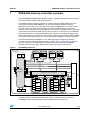
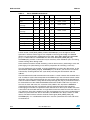
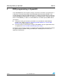
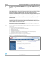
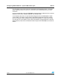
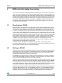
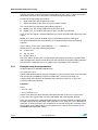
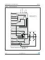
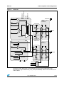
AN3132
Application note
Configuring the SPEAr600
multi-port memory controller (MPMC) for external DDR SDRAM
Introduction
The SPEAr600 embedded MPU features a multi-port memory controller for interfacing with
external DDR or DDR2 memory devices.
This application note describes how to configure the MPMC to use different types of DDR
and DDR2 memories and tune the parameters in accordance with JEDEC requirements and
the flexibility available in the application.
January 2010
Doc ID 16955 Rev 1
1/24
www.st.com
Contents
AN3132
Contents
1
SPEAr600 memory controller overview . . . . . . . . . . . . . . . . . . . . . . . . . 3
2
DDR overview . . . . . . . . . . . . . . . . . . . . . . . . . . . . . . . . . . . . . . . . . . . . . . 5
2.1
2.2
DDR2 vs. DDR1 . . . . . . . . . . . . . . . . . . . . . . . . . . . . . . . . . . . . . . . . . . . . . 5
2.1.1
Package differences . . . . . . . . . . . . . . . . . . . . . . . . . . . . . . . . . . . . . . . 7
2.1.2
Power supply differences . . . . . . . . . . . . . . . . . . . . . . . . . . . . . . . . . . . 8
2.1.3
Other feature differences . . . . . . . . . . . . . . . . . . . . . . . . . . . . . . . . . . . . . 8
Addressing . . . . . . . . . . . . . . . . . . . . . . . . . . . . . . . . . . . . . . . . . . . . . . . . . 8
3
DDR programming in Spear600 . . . . . . . . . . . . . . . . . . . . . . . . . . . . . . . 10
4
Configuring SPEAr MPMC for a specific DDR memory part . . . . . . . . 11
5
DDR controller delay lines tuning . . . . . . . . . . . . . . . . . . . . . . . . . . . . . 13
5.1
Reading from DRAM . . . . . . . . . . . . . . . . . . . . . . . . . . . . . . . . . . . . . . . . 13
5.2
Writing to DRAM . . . . . . . . . . . . . . . . . . . . . . . . . . . . . . . . . . . . . . . . . . . 13
5.2.1
Example using these parameters . . . . . . . . . . . . . . . . . . . . . . . . . . . . . 14
6
PCB layout recommendations . . . . . . . . . . . . . . . . . . . . . . . . . . . . . . . . 16
7
Pad descriptions and configurations . . . . . . . . . . . . . . . . . . . . . . . . . . 17
7.1
SSTLPAD_CFG_CTR register configuration . . . . . . . . . . . . . . . . . . . . . . 20
Appendix A Acronyms . . . . . . . . . . . . . . . . . . . . . . . . . . . . . . . . . . . . . . . . . . . . . . 22
Revision history . . . . . . . . . . . . . . . . . . . . . . . . . . . . . . . . . . . . . . . . . . . . . . . . . . . . 23
2/24
Doc ID 16955 Rev 1
AN3132
SPEAr600 memory controller overview
1
SPEAr600 memory controller overview
In the SPEAr600 embedded MPU, different memory controllers provide interfaces between
the system elements/blocks and external memory.
The MPMC multi-port memory controller is used for interfacing DDR (double data rate)
synchronous dynamic RAM (SDRAM). It is also responsible for reliable read-write
operations to the memory. In a powerful system like SPEAr600, there are several system
elements which may need to communicate with external DDR memory at any time to
increase system efficiency. This is possible because the memory provides data at very high
speed and system elements need time to process that data, so this time can be utilized by
other system elements to transfer data to/from the memory. For example, during the time
that the CPU processes some data or instructions, another master interface (CPU or DMA)
can read or write to the memory. This can be handled by the MPMC’s multi-port capablity.
For maximum flexibility the MPMC has one AHB slave port to configure the memory
controller registers and seven AHB slave ports for data. Figure 1: SPEAr600 architecture
gives an overview of the SPEAr600, showing the connections between the SDRAM
controller AHB data ports (M0,..,M6) and the various subsystems of the design.
Figure 1.
SPEAr600 architecture
SPEArPLUS
ARM subsystem
CPU1
ARM926EJS
16 KI/16 KD
coprocessor
cache
Tcm I/D I D
Configurable cell array subsystem
SRAM SRAM
32 KB 32 KB
APB
Int
ctr
Tmr
GPIO
ARM subsystem
CPU2
ARM926EJS
16 KI/16 KD
coprocessor
cache
Tcm I/D I D
APB
Tmr
Int
ctr
GPIO
Q
P
M0
O
N
M1
M
M2
M3
Multilayer bus interconnection matrix
MPMC
DDR1-2
6
45
F
2
31
1
3
G
6
H
Mtx
Cell array
(application
configurable)
Mtx
L
1234
1235
123
4
5
123
CFG
125
D
C
B
A
Mtx
UART
SPI
E
SPI
I2C
SRAM
32 KB
SRAM
32 KB
Tmr
Flash
NAND
GPIO
SPI
RAM
(8 KB)
WDG
RTC
GPIO
Sys
Ctr
ADC
IrDA
Low-speed connect
Misc
DMA
(8 channels)
CLCD
controller
Eth.
GMAC
USB2.0
Device
ROM
(32 KB)
USB2.0
Host
Flash
serial
USB2.0
Host
Application
subsystem
Basic subsystem
Common subsystems
M4
Tmr
M5
JPEG
(Codec)
Tmr
M6
UART
Mtx
Expi I/T
mux
R
HS connect.
In order to understand how the various IPs interact with the external memory through the
multi-port memory controller, the table below shows the driving masters present in
SPEAr600 and the corresponding memory controller AHB slave data port.
Doc ID 16955 Rev 1
3/24
SPEAr600 memory controller overview
Table 1.
AN3132
Memory controller AHB data ports
Memory controller AHB data port
Note:
Driving masters
M0
CPU2
M1
CPU1
M2
RAS_L, EXPI
N3
DMA master 1, RAS_H, EXPI
M4
Ethernet GMAC, RAS_Z
M5
USB subsystem
M6
RAS_E, CLCD controller
RAS_L, RAS_H , RAS_E and RAS_Z are specific ports that can be used in customized
SPEAr MPUs to connect masters to the external DDR.
This memory controller supports DDR1 and DDR2 devices following JEDEC standard up to
the clock frequency of 333MHz (data rate of 667 MT/sec). As the memory controller
supports DDR1 & DDR2 at different frequencies for almost all DDR part manufacturers,
MPMC must be programmed with the right timing parameters required for the selected DDR
memory part, selected DDR frequency, selected CAS latency etc.
This memory controller supports DDR1 and DDR2 devices, compliant with JEDEC
standards, up to a clock frequency of 333 MHz (data rate 667 MT/sec). As the memory
controller supports DDR1 and DDR2 at different frequencies for almost all DDR part
manufacturers, MPMC must be programmed with the right timing parameters required for
the selected DDR memory part, DDR frequency, CAS latency etc.
4/24
Doc ID 16955 Rev 1
AN3132
DDR overview
2
DDR overview
2.1
DDR2 vs. DDR1
DDR1 and DDR2 memory modules are widely used in desktop PCs. Their full name is DDR
(double data rate) SDRAM (synchronous DRAM), which is a variant of dynamic RAM.
Dynamic RAM differs from static RAM because the former, constituted by both transistors
and capacitors, requires constant refreshing to restore the values in the capacitors while the
latter, constituted only by transistors, does not require refreshing, resulting in much higher
performance. However, SRAMs are much more expensive than DRAMs.
Going back to SDRAM, this type of memory utilizes a synchronous interface: this means
that it waits for a clock pulse to transfer data, and thus it is synchronized with the system bus
and the processor. SDRAM transfers one bit (per data line) of data per clock cycle.
DDR SDRAM technology doubles the bandwidth of SDRAM under optimal conditions. In
fact, SDRAM transfers data on every clock cycle (to be specific, on the rising edge of every
clock cycle), while DDR transfers data on both the rising and the falling edge of a clock
cycle. Therefore, two bits (per data line) are transferred on every clock cycle. In order to do
this, two bits are accessed from the memory array (where data is actually stored) for each
data line on every clock cycle, this process is called the “2-bit prefetch”. In this way, the
interface’s clock speed remains constant, but the data bus effectively doubles in frequency.
The figure below shows a simple DDR1 SDRAM architecture example.
Figure 2.
DDR1 SDRAM architecture
In general, a DRAM (non synchronous) address is presented in two parts: a row and a
column address. The row and the column are multiplexed on the same set of address pins
(DDR_MEM_ADDR [14:0] with reference to SPEAr600 pins) to reduce package, size and
cost. First, the row address is loaded, or strobed, into the row address latch via the row
address strobe, or RAS, followed by the column address with the column address strobe, or
CAS. The Read data propagate to the output after a specified access time. Write data are
presented at the same time as the column address, because it is the column strobe that
actually triggers the transaction, whether read or write. The SDRAM internal state logic
operates on discrete commands that are presented to it. The signals RAS and CAS
(DDR_MEM_RAS and DDR_MEM_CAS, SPEAr600 pins) are still present, but they function
as part of other control signals to form commands rather than simple strobes.
Most of the input signals to the state logic shown in Figure 2 combine to form the discrete
commands listed in Table 2.
Doc ID 16955 Rev 1
5/24
DDR overview
AN3132
Table 2.
Basic SDRAM command set
Command
CS
RAS
CAS
WE
Address
AP/A10
Bank activate
L
L
H
H
Bank, row
A10
Read
L
H
L
H
Bank, column
L
Read with autoprecharge
L
H
L
H
Bank, column
H
Write
L
H
L
L
Bank, column
L
Write with autoprecharge
L
H
L
L
Bank, column
H
No operation
L
H
H
H
X
X
Burst terminate
L
H
H
L
X
X
Bank precharge
L
L
H
L
X
L
Precharge all banks
L
L
H
L
X
H
Mode register set
L
L
L
L
Configuration
Configuration
Auto refresh
L
L
L
H
X
X
Device deselect
H
X
X
X
X
X
A clock enable, CLKE (DDR_MEM_CLKEN, SPEAr600 pin), must be high for normal
operations. Interface control signals are sampled on the rising clock edge. As SDRAM
devices are manufactured in multibyte data bus width, Data (DDR_MEM_DQ, SPEAr600
pins) is a 16-bit wide bus in SPEAr600, the data mask DM (DDR_MEM_DM [1:0],
SPEAr600 pins) provides a convenient way to selectively mask individual bytes from being
written or being driven during reads.
Some common functions include activating a row for future access, performing a read, and
precharging a row (deactivating a row, often in preparation for activating a new row).
The first requirement, for example, to read an SDRAM is to activate the desired row, on the
desired bank (DDR_MEM_BA [2:0], SPEAr600 pins). To do this, you must use an activate
command by asserting RAS for one cycle while presenting the desired bank and row
address.
The next command issued to continue the transaction is a read. However the controller must
wait a number of cycles that corresponds to the DRAM array’s row-activate to column-strobe
delay time. To use the read command, you must assert CAS and present the desired bank
select and column address, along with the auto precharge (AP) flag. A particular bank must
be selected because the multibank SDRAM architecture enables reads from any bank. In
the case of reads and writes, the assertion of AP (address line 10) tells the SDRAM to
automatically precharge the activated row after the requested transaction completes.
Precharging a row returns it to quiescent state and also clears the way for another row in the
same bank to be activated next time. A single bank cannot have more than one row active at
any given time. Once the controller issues the read command, it must wait a predetermined
number of cycles before the data is returned by the SDRAM. This delay is known as CAS
latency. The data interface contains the data strobe signal (DDR_MEM_DQS [1:0],
SPEAr600 pins). It is a bidirectional clock that is used to synchronize the reads and writes
on the data bus.
6/24
Doc ID 16955 Rev 1
AN3132
DDR overview
Being a 2nd generation DDR, the most important improvement found in DDR2 memory is its
transfer data rate or bandwidth. As in the case of DDR SDRAM vs. SDRAM, the bandwidth
of DDR2 memory can double the bandwidth of DDR. DDR already operates on both the
rising and the falling edge of the clock, so DDR2 can achieve twice the bandwidth by
doubling the I/O buffer frequency. DDR2 utilizes a “4-bit prefetch” architecture: this means
that 4 bits of data are moved from the memory array to the I/O buffer per data line for each
core clock cycle. The core clock cycle refers to the cycle time of the memory array, and the
frequency of the memory array is half of the I/O buffers and ¼ of the data rates.
The table below compares the main features of DDR1 and DDR2.
Table 3.
DDR1 and DDR2 at a glance
DDR1
DDR2
Features
Frequency specifications
Data rate
200/266/333/400 Mbps
400/533/667 Mbps
Bus frequency
100/133/166/200 MHz
200/266/333 MHz
DRAM core frequency
100/133/166/200 MHz
100/133/166 MHz
Prefetch size
2 bit
4 bit
Burst length
2/4/8
4/8
Data strobe
Single DQS
Differential Strobe: DQS, /DQS
CAS latency
1.5, 2, 2.5
3, 4, 5
Write latency
1T
Read latency-1
Power Specs
Core voltage (VDD)
2.5 V
1.8 V
I/O voltage (VDDQ)
SSSTL_2(2.5 V)
SSSTL_1.8(1.8 V)
Format
Packaging
TSOP(II), TBGA
FBGA
Compatibility with DDR1
Command Set
Same as DDR1
Parameters
Same as DDR1
Bus Utilization and Signal Integrity
ODT
OCD calibration
New features
Posted CAS
Additive latency
2.1.1
Package differences
DDR2 memories have smaller size packages with less electrical noise, thus resulting in
improved integrity at higher operating frequencies.
Doc ID 16955 Rev 1
7/24
DDR overview
2.1.2
AN3132
Power supply differences
DDR2 operates at 1.8 V. This is a 28% reduction compared to DDR1, which combined with
power saving features such as smaller page sizes and an active power down mode results
in power consumption advantages.
2.1.3
Other feature differences
DDR2 has also some other new features like on die termination (ODT). Around the memory
slots on a DDR1-supporting motherboard, there can be termination resistors, which are
used to eliminate excessive signal noise. For DDR2 modules, the termination resistors are
built into the chip, which are far closer to the source of the noise. This ODT feature can
reduce interference within the chip, thus guaranteeing the stability and reliability of DDR2
memory when working under high frequencies.
There are other features such as Posted CAS and Additive latency, which work together to
prevent data collisions and utilize the data bus more efficiently, as well as the off-chip driver
calibration (OCD), which increases signal integrity and system timing margin as well.
2.2
Addressing
Once configured, you do not need to to worry about the DDR protocol; you can access the
DDR by directly accessing the memory address. In SPEAr600, DDR is mapped from
0x0000_0000 to 0x3FFF_FFFF: that means that an addressable space of 1 GB is dedicated
to the external DRAM. In this way you can address, using all the 30 address bits, up to 2 x 4
Gb memory chips. Only 256 Mb x 16 cuts are possible because of the presence of only 14
address lines, DDR_MEM_ADDR [14:0]. In this case, the use of the bits is divided in the
following way:
●
10 bits for column address
●
3 bits for bank address
●
15 bits for row address
In the user address, bit 0 is used to select the width of the datapath. It is fixed to ‘0’ if the
datapath is 16 bit and if the datapath is 8 bit, it is fixed to ‘1’.
So in this case:
●
User_address [0] = datapath;
●
User_address [10:1] = column address;
●
User_address [13:11] = bank address;
●
User_address [28:14] = row address;
●
User_address [29] = chip select;
Regardless of the memory cut selected, the CPU always sees a contiguous addressable
space. For this reason, the memory controller always shifts the memory address parts (row,
bank and column) in the user address according to the physical memory cut attached and
its configuration.
8/24
Doc ID 16955 Rev 1
AN3132
DDR overview
For example, the situation for the cut 128 Mb x 8 in eight and four bank mode is shown
below:
●
●
128 Mb x 8 (eight bank mode, all 3 bank address bits are used)
–
User_address [0] = datapath;
–
User_address [10:1] = column address;
–
User_address [13:11] = bank address;
–
User_address [27:12] = row address;
–
User_address [28] = chip select;
128 Mb x 8 (four bank mode, only 2 bits are used for the bank address)
–
User_address [0] = datapath;
–
User_address [10:1] = column address;
–
User_address [12:11] = bank address;
–
User_address [26:13] = row address;
–
User_address [27] = chip select;
SPEAr600 supports DDR1 and DDR2 devices. The memory controller needs to be
configured once at system startup depending on the memory type, size, and vendor and on
the frequency you want to work with.
Doc ID 16955 Rev 1
9/24
DDR programming in Spear600
3
AN3132
DDR programming in Spear600
In the SPEAr600 LSP (Linux support package), the memory controller is programmed in a
small piece of firmware executed just after boot ROM code and named “Xloader”. The
standard Xloader provided by STMicroelectronics is coded for the DDR2 device installed on
the ST SPEAr600 evaluation board. The memory part available on ST’s evaluation board is
either an mt47H64M16_3 1-Gbit or an mt47H32M16 viz. 512-Mbit capacity DDR2 device.
You need to:
●
Change the setting of the memory controller in case of different vendor /different
memory sizes. Refer to Section 4: Configuring SPEAr MPMC for a specific DDR
memory part for the procedure to follow.
●
Fine tune the DLL to find the best settings of the MPMC in the your application board,
as explained in Section 5: DDR controller delay lines tuning.
The objective of the next two sections is to provide all the information you need to customize
the “general purpose” MPMC settings provided by ST, modifying them to match your
application requirements.
10/24
Doc ID 16955 Rev 1
AN3132
4
Configuring SPEAr MPMC for a specific DDR memory part
Configuring SPEAr MPMC for a specific DDR memory
part
Many timing parameters such as CAS latency, Trc, refresh timings etc. need to be fulfilled for
reliable DDR read/writes. These timing parameters become much more important at higher
frequencies like 333 MHz or 666 MT/seconds. You need to configure these timing
parameters in the MPMC registers at system startup before using DDR. Although almost all
DDR manufacturers fulfil the JEDEC specifications, still these timing parameters vary
slightly with different memory manufacturers and also for different memory parts within the
same DDR manufacturer. So you must program the SPEAr MPMC register to configure the
timing parameters based on the memory device and the clock frequency in use on the
application board.
For many MPMC registers, you need to convert the timings mentioned in the memory
datasheet to number of clock cycles according to the required frequency. After the
conversion, these values must be written to the correct bit field location in the right register
address of MPMC: this requires careful study.
To help you, ST provides a Web tool giving the complete MPMC register configuration for
SPEAr devices and for each selected DDR part.
Note:
To access the Web tool for generating the register configuration file, please contact your ST
representative.
You need to provide the following information:
1.
Product name, for example SPEAr600 or SPEAr300
2.
DDR part to be used
3.
Required DDR frequency
4.
CAS latency supported by the selected DDR part at the selected frequency
5.
Required burst length (fixed to 4 in case of DDR2)
The figure below shows a snapshot of the page of the Web tool.
Figure 3.
ST SPEAr600 configuration manager
Doc ID 16955 Rev 1
11/24
Configuring SPEAr MPMC for a specific DDR memory part
AN3132
This tool allows you to select memories and request the configuration values. A progress
page is displayed while the script runs, and the file can be downloaded when the script
completes.
Once the configuration values for SPEAr600 are obtained from the Web tool for the selected
DDR part, these values should be updated in the Xloader code.
In the Xloader code, there are separate DDR configuration files for SPEAr600 in a folder
named “DDR”. You need to create another similar DDR configuration file for the memory
part in use with the values received from the Web tool. Moreover, it is necessary to make
sure that the PLL of the SPEAr system used to clock DDR is programmed for the selected
DDR frequency. Refer to the miscellaneous block chapter of the SPEAr600 user manual for
details.
12/24
Doc ID 16955 Rev 1
AN3132
5
DDR controller delay lines tuning
DDR controller delay lines tuning
There are certain JEDEC timing requirements for DDR signals on the memory part side for
writes and at the controller side for reads. All DRAM and memory controller manufacturers
follow these timing specifications for reliable data read/write. Because of PCB properties (for
example, track lengths, impedance, device Substrate, memory loading, etc), it is necessary
to tune these signals/parameters in order to be in accordance with the specifications and
maximize the specifications margin for the signals at DRAM and memory controller side.
This tuning can be done by delaying/shifting the signals (DQS and data) with respect to
each other and the core clock.
5.1
Reading from DRAM
DDR (dual data rate) memories send a data strobe (DQS) signal coincident with the read
data so that the read data can be reliably captured by the memory controller. The edges of
this strobe are aligned with the data output by the DRAM devices. The paths for the data
and the associated data strobe signals should be routed with the same length between the
capture logic and the DRAM devices, allowing the rising and falling edges of the data strobe
to arrive at the capture logic at the same time the data is in transition. However, the raw data
strobe signal cannot be used as a clock to capture the data, since the data will not be stable
when the data strobe edges are rising and falling. Instead, a delayed version of the data
strobe signal must be used to capture the data. The delay added to the data strobe signals
should be such that the margin to capture the read data is maximized. Because the
frequency of the data strobe signal is matched to the system clock, the delay is a relative
number based on the period of the system clock.
On SPEAr devices, this delay is managed by dll_dqs_delay_1 and dll_dqs_delay_0
parameters (MPMC_Register_39, at offset 0x9C from base address of MPMC) respectively
for upper 8 bits and lower 8 bits of the memory datapath.
5.2
Writing to DRAM
DDR memories require that the DQS data strobe arrives at the DDR within a certain window
around the clock. This value (tdqss) is specified in fractions of a clock cycle. Most DRAM
devices specify this value between +/- 0.25 and 0.2 of a clock cycle. This translates to a
valid window of between 0.5 and 0.4 of a clock cycle.
The DRAM devices expect the data strobe signal to be shifted by the memory controller in
order to allow the DRAM the maximum margin for capturing the data with the data strobe
signal sent to the DRAM devices from the memory controller.
The DLL maintains two delay lines for sending write data and the write data strobe. The first
delay line delays the main clock so that the write data strobe transition reaches the DRAM
as synchronously as possible with the clock edge under typical operating conditions. The
second delay line adjusts the clock that is used to output the write data. This clock should be
adjusted to maximize the setup and hold requirements around the write strobe.
Both the DQS (for write) and Data (DQ) signals from the SPEAr device are controlled by the
programmable parameters dqs_out_shift (MPMC_Register_40, at offset 0xA0 from base
address of MPMC) and wr_dqs_shift (MPMC_Register 41, at offset 0xA4 from base address
of MPMC). These two parameters for writes are valid for both bytes that constitute the
Doc ID 16955 Rev 1
13/24
DDR controller delay lines tuning
AN3132
memory data path, in contrast to the read parameters dll_dqs_delay_x. These parameters
allow these two clocks to be delayed by a fixed percentage of the core clock.
In short, for writing to DDR you need to:
1.
Align DQS signal with respect to the clock
2.
Adjust DQ signals to the specs (1/4 cycle) relative to DQS.
This can be done by programming the following registers:
●
MPMC_CTL_40: to align DQS (write) to the clock signal
●
MPMC_CTL_41: to adjust DQ signal to within 1/4 clock cycle of DQS.
There is only one register, mentioned previously, to center the read DQS signal in the clock
signal:
MPMC_CTL_39: to activate the DQS signal in the middle of the data valid signal
The delay introduced by these parameters can be determined based on the following
equation,
Delay = delays in one cycle *param [6:0]/128. ----------- (Equation 1)
Where param is one of the following parameters:
●
wr_dqs_shift
●
dqs_out_shift
●
dll_dqs_delay_X
The value “delays in one cycle” is automatically generated by the memory controller DCC
(delay compensation circuit) master delay line that calculates the number of delay elements
that constitute a complete cycle in an adaptive way (according to PVT variations).
5.2.1
Example using these parameters
At DDR frequency of 333 MHz (666 MT/sec):
One cycle time = 3 ns
If Write DQS generated by the memory controller is in phase with the clock on the controller
side and also at the DRAM end (effects of PCB tracks, substrate track length are
compensated), then DQS can be aligned to the clock by two values of wr_dqs_shift
parameter which are 0 or 0x7F.
Equation 1
Delay
= 3 ns x 0 = 0 or
= 3 ns x 128/128 = 3 ns
In both cases either the delay between write DQS and clock is zero or 3 ns (one clock
cycle), so the two signals which are Data strobe/DQS and clock would be aligned.
But in actual scenarios, the write DQS generated by the memory controller is slightly shifted.
At higher frequencies like 333 MHz, clock cycle time is very small (3 ns) and a deviation of
more than ¼ clock cycle time is not accepted. So we need to change this parameter value
from its ideal value of 0x0 or 0x7F. Just for reference, the value for this parameter in the
SPEAr600 evaluation board is 0x72.
14/24
Doc ID 16955 Rev 1
AN3132
DDR controller delay lines tuning
Similarly to make the DQ signal within ¼ clock time of DQS, according to Equation 1 the
value 0x5F would be in an ideal scenario. Off course we need to tune this parameter
because of the same above mentioned reason. Just for reference, the value for this
parameter for in the SPEAr600 evaluation board is 0x55.
During reading from DRAM, memories send data strobe (DQS) signal coincident with the
read data. In Ideal scenarios to make DQS signal in the middle of data valid window, we
need to delay DQS signal by ¼ of clock cycle as data is read on both rising & falling edges.
So the value of the dll_dqs_delay_X parameter should be 0x1F according to Equation 1. In
practice, you need to tune this value as per the board and device. The value used in the
SPEAr600 evaluation board for this parameter is 0x0A for both dll_dqs_delay_X
parameters.
Doc ID 16955 Rev 1
15/24
PCB layout recommendations
6
AN3132
PCB layout recommendations
Layout and PCB parameters play a very important role for DDR, especially when the system
runs at high frequencies like 333 MHz (667 MT/sec).
AN2797 PCB layout guidelines for SPEAr600 provides recommendations for DDR signal
routing, track lengths and impedances. Please strictly follow these guidelines. This
application note also provides the required data to balance the length of the data/control
tracks going to the DDR chips.
PCB simulation is also strongly suggested to make sure that PCB does not introduce signal
reflection and to determine violations in the communication between MPMC and DDR. The
IBIS model of the DDR interface of SPEAr600 is available to run these simulations. Refer to
AN2715 IBIS models for signal integrity simulation of SPEAr600 applications.
The schematics and layouts of the SPEAr600 evaluation board is available and can be used
as reference design and starting point for your application design.
16/24
Doc ID 16955 Rev 1
AN3132
7
Pad descriptions and configurations
Pad descriptions and configurations
To ensure correct behavior of the memory controller in any application, you need to properly
configure the various pads that interface the DDR memory.
The following table contains the complete list of the SPEAr600 pads involved with the use of
DDR.
Table 4.
SPEAr600 memory controller pads
Signal
Pad type
Direction
DDR_MEM_COMP2V5_REXT ANA_2V5_STAG
DDR_MEM_COMP1V8_REXT ANA_1V8_STAG
DDR_MEM_ADDR[14:0]
BDPROGDDRSCARUDQP_VDDE/GNDE_1V8_2V5_NORES_STAG
OUT
DDR_MEM_RAS
BDPROGDDRSCARUDQP_VDDE/GNDE_1V8_2V5_NORES_STAG
OUT
DDR_MEM_CAS
BDPROGDDRSCARUDQP_VDDE/GNDE_1V8_2V5_NORES_STAG
OUT
DDR_MEM_WE
BDPROGDDRSCARUDQP_VDDE/GNDE_1V8_2V5_NORES_STAG
OUT
DDR_MEM_CS[1:0]
BDPROGDDRSCARUDQP_VDDE/GNDE_1V8_2V5_NORES_STAG
OUT
DDR_MEM_BA[2:0]
BDPROGDDRSCARUDQP_VDDE/GNDE_1V8_2V5_NORES_STAG
OUT
DDR_MEM_CLKEN
BDPROGDDRSCARUDQP_VDDE/GNDE_1V8_2V5_NORES_STAG
OUT
DDR_MEM_GATE_OPEN[1:0] BDPROGDDRSCARUDQP_VDDE/GNDE_1V8_2V5_NORES_STAG
INOUT
DDR_MEM_ODT[1:0]
BDPROGDDRSCARUDQP_VDDE/GNDE_1V8_2V5_NORES_STAG
OUT
DDR_MEM_DM[1:0]
BDPROGDDRSCARUDQP_VDDE/GNDE_1V8_2V5_NORES_STAG
OUT
DDR_MEM_DQS[1:0]
BDCLKDDRSCARUDQP_1V8_2V5_NORES_STAG
INOUT
nDDR_MEM_DQS[1:0]
BDCLKDDRSCARUDQP_1V8_2V5_NORES_STAG
INOUT
DDR_MEM_DQ[15:0]
BDPROGDDRSCARUDQP_VDDE/GNDE_1V8_2V5_NORES_STAG
INOUT
DDR_MEM_CLKP
BDCLKDDRSCARUDQP_1V8_2V5_NORES_STAG
OUT
DDR_MEM_CLKN
BDCLKDDRSCARUDQP_1V8_2V5_NORES_STAG
OUT
DDR_MEM_VREF
VREFSSTL_1V8_STAG
DDR2_EN
BD2TARUQP_3V3_STAG
IN
Except for some reference pads, all the pads can be divided into two main groups on the
basis of the nature of the digital cell present in the pad:
●
Data cell (BDPROGDDRSCARUDQP_VDDE/GNDE_1V8_2V5_NORES_STAG)
●
Clock cell (BDCLKDDRSCARUDQP_1V8_2V5_NORES_STAG)
The figures below show the data cell and clock cell architecture.
Doc ID 16955 Rev 1
17/24
Pad descriptions and configurations
VDDE2V5
VDD
A[0:6]SRC2V5
Data cell architecture
REFSSTL
Figure 4.
AN3132
EN
A0SRC2V5 to A6SRC2V5
for 1.8 V or 2.5 V
Compensation ASRC code
TEN
TM
A
TA
DDR2V5
ZOUTPROGA2V5
PROGA2V5, PROGB2V5
ENZI
RTT = RVAL1/2 or RVAL2/2
ZI
150 Ω
MODEZI2V5
REFSSTL
150 Ω
PU2V5
PDN2V5
ODTRES
ODTEN
GND GNDE
18/24
Doc ID 16955 Rev 1
150 Ω
150 Ω
AN3132
VDDE2V5
VDD
A[0:6]SRC2V5
Clock cell
REFSSTL
Figure 5.
Pad descriptions and configurations
EN
VDDEPAD
On-die
termination
TEN
DDR2V5
ZOUTPROGA2V5
PROGA2V5, PROGB2V5
TM
A
TA
PUPCLK2V5
50 kΩ
150 Ω
150 Ω
IOCLK
50 kΩ
150 Ω
150 Ω
PDNCLK2V5
Output part
Pull-up and
pull-down
SEP
On-die
termination
DDR2V5
MODEZI2V5
ENZI
PDN2V5
ZI
50 kΩ
DDR2V5
MODEZI2V5
150 Ω
IOCLKB
50 kΩ
SEN
DDR2V5
MODEZI2V5
150 Ω
150 Ω
150 Ω
PU2V5
Input part
Pull-up and
pull-down
GND
GNDE
ODTRES
ODTEN
STRB
All the pins of the digital cells are controlled on the basis of the configuration of the
Miscellaneous register SSTLPAD_CFG_CTR (0xFCA800F0). Refer to the User Manual for
further details.
Doc ID 16955 Rev 1
19/24
Pad descriptions and configurations
7.1
AN3132
SSTLPAD_CFG_CTR register configuration
The pads should be configured according to the type of memory in use (DDR1 or DDR2)
In the SSTLPAD_CFG_CTR register, Bits [19:16] and bit [0] are used in conjunction with
pin DDR2_EN to configure the pads in hardware or software mode.
●
Bits [19:16] = 0000: hardware configuration mode.
In this mode, the input level of the DDR2_EN pin selects the configuration
(DDR2_EN =1 = configuration for DDR2) and DDR_PAD register [0] is don’t care.
●
Bits [19:16] = 0110: software configuration mode.
In this mode, the value of DDR_PAD register [0] selects the configuration]
(1 = configuration for DDR2) and pin DDR2_EN is don’t care.
All other combinations are not allowed.
Bit [15] is a status bit and reflects the status of the pin DDR2_EN.
All the other combinations are not allowed.
All these settings establish the value for the pin DDR2V5 of pad data and clock cells and
configure them to operate properly on the basis of the memory type attached.
Bit [14] establishes the nature of the common reference for all SSTL pads.
0 = internal reference and
1 = external reference.
It is recommended to use an external reference to improve the stability.
Bit [12] decides the nature of the clock cells: fully differential (differential) or pseudodifferential (single ended). This bit controls the pin STRB of the pad clock cell, but only for
the pads DDR_MEM_DQS [1:0] . When in DDR1 mode the bit 12 must be set to 1 to put the
pads in single ended mode.
For the pad DDR_MEM_CLKP/N the pin STRB is blocked to 0. These pads operate in
differential mode both in DDR1 and DDR2 operating mode.
Bits [11:10] respectively control the pull-up and the pull-down of pins PDNCLKB2V5 and
PUPCLKB2V5 of the pad clock cells for the DDR_MEM_DQS[1:0] pads.See Table 5 for the
settings.
Bits [9: 8] respectively control the pull-up and the pull-down of pins PDNCLK2V5 and
PUPCLK2V5 of the pad clock cells for the DDR_MEM_DQS[1:0] pads.See Table 5 for the
settings.
Bits [7: 6] respectively control the pull-up and the pull-down of pins PDNCLK2V5 and
PDNCLKB2V5 of the pad clock cell for the DDR_MEM_CLKP/N pads.See Table 5 for the
settings.
Bits [5: 4] control the pull-up and the pull-down of the pins PU2V5 and PDN2V5 of all pad
data cells.See Table 5 for the settings.
Table 5.
Pull-up and pull down settings
Bit pair value
20/24
Meaning
00
pull-down active and pull-up not active
01
forbidden
Doc ID 16955 Rev 1
AN3132
Pad descriptions and configurations
Table 5.
Pull-up and pull down settings (continued)
Bit pair value
Meaning
10
pull-down not active and pull-up not active (default)
11
pull-down not active and pull-up active
The bit 3, bit 2 and bit 1 control respectively the pins ZPROGOUTA2V5, PROGA2V5,
PROGB2V5 for all pad data and clock cells.
The following notes apply to these three bits:
●
They are independent, but not completly uncorrelated. All 8 combinations are valid, but
are partially overlapping.
●
They are board dependent, and must be determined during the tuning phase for every
PCB type.
●
They depend on the PCB characteristic impedance and the frequency of the DDR
signals.
Bit [3], the drive mode bit, changes the output impedance of the pad and must be set in
accordance with the PCB load.
It must be set to 0 (strong mode) when the characteristic impedance of the PCB is up to 50
Ohm.
It must be set to 1 (weak mode) when the characteristic impedance of the PCB is from 50 to
70 Ohm.
Bits [2] and [1 ), prog_a and prog_b, set the “way” the internal transistors of the pad are
loaded as well as the resulting effect on the slope of the signal. These 2 bits define 4
increments of increasing capability: from 00 (slower slope) to 11 (higher slope). All
intermediate values are valid.
When you deal with high frequency signals, you should configure higher slopes to increase
the data valid window, keeping in mind that the higher the slope, the more the signal
reflection.
Doc ID 16955 Rev 1
21/24
Acronyms
AN3132
Appendix A
Table 6.
22/24
Acronyms
Acronyms used in this document
Acronym
Definition
ARM
Advanced RISC machine
CETK
Windows CE test kit
DDR
Double data rate SDRAM
DLL
Delay locked loop
DQ
DDR data
DQS
DDR data strobe
FAT
File allocation table
LSP
Linux support package
MPMC
Multi-port memory controller
USB
Universal serial bus
Doc ID 16955 Rev 1
AN3132
Revision history
Revision history
Table 7.
Document revision history
Date
Revision
06-Jan-2010
1
Changes
Initial release.
Doc ID 16955 Rev 1
23/24
AN3132
Please Read Carefully:
Information in this document is provided solely in connection with ST products. STMicroelectronics NV and its subsidiaries (“ST”) reserve the
right to make changes, corrections, modifications or improvements, to this document, and the products and services described herein at any
time, without notice.
All ST products are sold pursuant to ST’s terms and conditions of sale.
Purchasers are solely responsible for the choice, selection and use of the ST products and services described herein, and ST assumes no
liability whatsoever relating to the choice, selection or use of the ST products and services described herein.
No license, express or implied, by estoppel or otherwise, to any intellectual property rights is granted under this document. If any part of this
document refers to any third party products or services it shall not be deemed a license grant by ST for the use of such third party products
or services, or any intellectual property contained therein or considered as a warranty covering the use in any manner whatsoever of such
third party products or services or any intellectual property contained therein.
UNLESS OTHERWISE SET FORTH IN ST’S TERMS AND CONDITIONS OF SALE ST DISCLAIMS ANY EXPRESS OR IMPLIED
WARRANTY WITH RESPECT TO THE USE AND/OR SALE OF ST PRODUCTS INCLUDING WITHOUT LIMITATION IMPLIED
WARRANTIES OF MERCHANTABILITY, FITNESS FOR A PARTICULAR PURPOSE (AND THEIR EQUIVALENTS UNDER THE LAWS
OF ANY JURISDICTION), OR INFRINGEMENT OF ANY PATENT, COPYRIGHT OR OTHER INTELLECTUAL PROPERTY RIGHT.
UNLESS EXPRESSLY APPROVED IN WRITING BY AN AUTHORIZED ST REPRESENTATIVE, ST PRODUCTS ARE NOT
RECOMMENDED, AUTHORIZED OR WARRANTED FOR USE IN MILITARY, AIR CRAFT, SPACE, LIFE SAVING, OR LIFE SUSTAINING
APPLICATIONS, NOR IN PRODUCTS OR SYSTEMS WHERE FAILURE OR MALFUNCTION MAY RESULT IN PERSONAL INJURY,
DEATH, OR SEVERE PROPERTY OR ENVIRONMENTAL DAMAGE. ST PRODUCTS WHICH ARE NOT SPECIFIED AS "AUTOMOTIVE
GRADE" MAY ONLY BE USED IN AUTOMOTIVE APPLICATIONS AT USER’S OWN RISK.
Resale of ST products with provisions different from the statements and/or technical features set forth in this document shall immediately void
any warranty granted by ST for the ST product or service described herein and shall not create or extend in any manner whatsoever, any
liability of ST.
ST and the ST logo are trademarks or registered trademarks of ST in various countries.
Information in this document supersedes and replaces all information previously supplied.
The ST logo is a registered trademark of STMicroelectronics. All other names are the property of their respective owners.
© 2010 STMicroelectronics - All rights reserved
STMicroelectronics group of companies
Australia - Belgium - Brazil - Canada - China - Czech Republic - Finland - France - Germany - Hong Kong - India - Israel - Italy - Japan Malaysia - Malta - Morocco - Philippines - Singapore - Spain - Sweden - Switzerland - United Kingdom - United States of America
www.st.com
24/24
Doc ID 16955 Rev 1