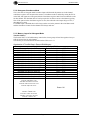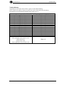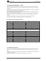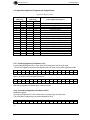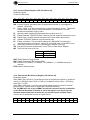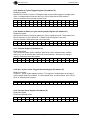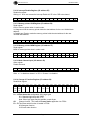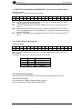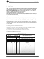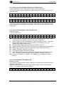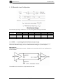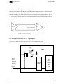
1
HYTEC ELECTRONICS Ltd
5 CRADOCK ROAD, READING, BERKS. RG2 0JT, UK
Telephone: +44 (0) 118 9757770
Fax: +44 (0)118 9757566
E-mail: [email protected]
Copyright 2011, Hytec Electronics Ltd
Data and specifications are subject to change without notice
MCS8522
MULTI-CHANNEL SCALER
INDUSTRY PACK
USERS MANUAL
PCB Issue 1.0
Firmware Versions:
Histogram Mode LVDS\TTL V103
Histogram Mode LVDS\TTL V104
Histogram Mode LVDS\TTL V105
Preset Scaler Mode LVDS\TTL V103
Document Nos.: MCS8522/UTM/G/x/3.0
Date: 18/12/2014
Author: MRN
Hytec Electronics Ltd
MCS8522/UTM/3.0
Revision History
The following table shows the revision history for this document.
Date
Version
30/05/12
1.0
25/07/12
1.1
27/07/12
04/09/12
2.0
2.1
18/12/14
3.0
Revision
Initial release.
FF flag put in CSR.
Unit does not start when nos cycles/triggers is set to zero.
Unit does not start in Hist mode when Nos Gates per cycle is set to
zero.
Enter value required as opposed to not one less.
Mem address reg in straight scaler mode shows next memory
location to be written to.
Dual boot for histogram mode or Preset scaler mode
I/O configuration section expanded and added to contents page.
In Histogram Mode add External Enable function and amend TTL
logic level register to include External Enable bit level.
CRITICAL APPLICATIONS DISCLAIMER
THIS PRODUCT FROM HYTEC ELECTRONICS LTD USES COMPONENTS THAT ARE NOT
DESIGNED OR INTENDED TO BE FAIL-SAFE, OR FOR USE IN ANY APPLICATION REQUIRING
FAIL-SAFE PERFORMANCE, SUCH AS IN LIFE-SUPPORT OR SAFETY DEVICES OR SYSTEMS,
CLASS III MEDICAL DEVICES, NUCLEAR FACILITIES, APPLICATIONS RELATED TO THE
DEPLOYMENT OF AIRBAGS, OR ANY OTHER APPLICATIONS THAT COULD LEAD TO DEATH,
PERSONAL INJURY OR SEVERE PROPERTY OR ENVIRONMENTAL DAMAGE (INDIVIDUALLY AND
COLLECTIVELY, “CRITICAL APPLICATIONS”).
FURTHERMORE, SOME COMPONENTS USED IN THIS HYTEC ELECTRONICS LTD PRODUCTS ARE
NOT DESIGNED OR INTENDED FOR USE IN ANY APPLICATIONS THAT AFFECT CONTROL OF A
VEHICLE OR AIRCRAFT, UNLESS THERE IS A FAIL-SAFE OR REDUNDANCY FEATURE AND A
WARNING SIGNAL UPON FAILURE TO THE OPERATOR.
THE CUSTOMER ASSUMES THE SOLE RISK AND LIABILITY OF ANY USE OF HYTEC
ELECTRONICS LTD PRODUCT IN CRITICAL APPLICATIONS.
Page 2
Hytec Electronics Ltd
MCS8522/UTM/3.0
CONTENTS
1.
INTRODUCTION ......................................................................................................................... 5
2.
MODES OF OPERATION........................................................................................................... 6
2.1
2.2
2.3
HISTOGRAMMING MODE .......................................................................................................... 6
STRAIGHT SCALER MODE ........................................................................................................ 6
PRESET SCALER MODE ............................................................................................................ 6
3.
PRODUCT SPECIFICATIONS .................................................................................................. 7
4.
LOGIC SIGNAL LEVELS ........................................................................................................... 8
5.
HISTOGRAM AND STRAIGHT SCALER OPERATING MODES ...................................... 9
5.1
HISTOGRAM MODE (MD0=’0’ IN CSR) .................................................................................. 9
5.1.1
Basic Histogram Mode .................................................................................................... 9
5.1.2
Histogram Coincidence Mode ....................................................................................... 10
5.1.3
Memory Layout for Histogram Mode............................................................................ 10
5.2
STRAIGHT SCALER MODE (MD0=’1’ IN CSR)...................................................................... 12
5.2.1
Memory Layout Straight Scaler Mode .......................................................................... 12
5.3
AUTOMATED MEMORY CLEAR ............................................................................................. 12
5.4
APPLICATION REGISTERS HISTOGRAM AND STRAIGHT SCALER ........................................... 13
5.4.1
Counting Registers (I/O Address 0-31) ......................................................................... 13
5.4.2
Coincidence Registers (I/O Address 32-47) .................................................................. 13
5.4.3
Control & Status Register (CSR I/O Address 48).......................................................... 14
5.4.4
Gate Interval (Bin Advance) Register (I/O address 49) ................................................ 14
5.4.5
Number of Cycles\Triggers Register (I/O address 50).................................................. 15
5.4.6
Number of Gates per cycle (memory depth) Register (I/O address 51) ........................ 15
5.4.7
Overflow Register (I/O address 52)............................................................................... 15
5.4.8
Nos "Cycles" and/or Triggers Received Register (IP address 53)................................ 15
5.4.9
Interrupt Vector Register (I/O address 54) ................................................................... 15
5.4.10 Interrupt Disable Register (I/O address 55) ................................................................. 16
5.4.11 Memory pointer LSW Register (I/O address 56) ........................................................... 16
5.4.12 Memory pointer MSW Register (I/O address 57).......................................................... 16
5.4.13 Mask Channel Input (I/O address 58) ........................................................................... 16
5.4.14 Change of Function Register (I/O address 59) ............................................................. 16
5.5
SELECT TTL LEVEL REGISTER (I/O ADDRESS 60) (ONLY IN VERSION V105 AND ABOVE).. 17
5.5.1
Counter Source (I/O address 62)................................................................................... 17
5.6
INTERNAL AND EXTERNAL RESET ......................................................................................... 17
5.7
EXTERNAL TIME BIN ADVANCE (EBA)................................................................................. 18
5.8
EXTERNAL TRIGGER ENABLE (ONLY IN VERSION V104 AND ABOVE) .................................. 18
5.9
MINIMUM DWELL TIME................................................................................................... 19
6.
PRESET SCALER....................................................................................................................... 20
6.1
SETTING VALUE TO LOAD IN TO PRESET SCALER ................................................................. 20
6.2
APPLICATION REGISTERS PRESET SCALER ............................................................................ 20
6.2.1
Preset Counting and Shadow Registers (I/O Address 0-31) ......................................... 21
6.2.2
Control & Status Register (CSR I/O Address 48).......................................................... 21
6.2.3
Preset Hit Register (I/O address 52) ............................................................................. 21
6.2.4
Count Termination Mask Register (IP address 53)....................................................... 22
6.2.5
Interrupt Vector Register (I/O address 54) ................................................................... 22
6.2.6
Interrupt Disable Register (I/O address 55) ................................................................. 22
6.2.7
ARM Channel Input (I/O address 58)............................................................................ 22
6.2.8
Change of Function Register (I/O address 59) ............................................................. 22
6.2.9
Select TTL level (I/O address 60) .................................................................................. 23
Page 3
Hytec Electronics Ltd
MCS8522/UTM/3.0
6.2.10 Counter Source (I/O address 62)................................................................................... 23
6.3
INTERNAL AND EXTERNAL RESET PRESET SCALER MODE .................................................... 23
7.
ID PROM...................................................................................................................................... 24
8.
I/O STANDARDS INPUT CONFIGURATION...................................................................... 25
8.1
8.2
8.3
LVPECL — LOW VOLTAGE POSITIVE EMITTER COUPLED LOGIC ....................................... 25
LVDS — LOW VOLTAGE DIFFERENTIAL SIGNAL ................................................................. 26
J1 PULL-UP OR PULL-DOWN FOR TTL LOGIC SIGNALS ......................................................... 26
APPENDIX A....................................................................................................................................... 27
APPENDIX B....................................................................................................................................... 28
APPENDIX C....................................................................................................................................... 29
APPENDIX D....................................................................................................................................... 30
Page 4
Hytec Electronics Ltd
MCS8522/UTM/3.0
1. INTRODUCTION
The Hytec IP-MSC-8522 is a single-width Industry Pack that provides 16 scalers channels
with the following characteristics:•
•
•
•
•
•
•
•
•
•
•
•
•
•
•
•
•
•
•
•
•
•
16 independent counting channels.
32-bit counter depth.
Shadow register to allow on-the-fly reading of scalers.
Full 32 bits binary count capacity and 64 bit histogram capability.
2Mbytes SRAM.
Gate/Bin advance by internal timer or programmable number of external pulses.
200MHz Count rates (LVDS, LVPECL and NIM), 100MHz for TTL.
TTL, LVDS and LVPECL inputs (Input type must be specified when ordered).
Input type can be reconfigured in the field via the JTAG port if requirements change.
NIM input via dedicated terminal block.
Each scaler has a 16 bit input coincidence pattern register.
Interrupt on completion of programmed number of cycles/triggers/counts.
External hardware trigger (software enable) or software trigger.
Trigger output to allow Trigger In / Out daisy-chain connection for synchronisation.
Software and external hardware reset of scalers and memory.
Scaler external inputs via transition board.
Trigger ignored if cycle has not completed.
Channel masking.
Counter Overflow register.
Number of Cycle/Triggers Received register.
The ability to read the module identity, manufacturer, model, revisions, input type and
serial number from an onboard ID ROM.
In the field firmware upgrade capability.
Page 5
Hytec Electronics Ltd
MCS8522/UTM/3.0
2. Modes of Operation
2.1 Histogramming Mode
In this mode a histogram is formed for each channel. This is achieved by acquiring and
logging the data for each channel over a number of programmable time intervals (gates/bins)
for a programmable number of cycles.
•
•
•
•
•
•
•
•
Gate/Bin advance by internal timer or programmable number external pulses (1 to
65525).
Internal Gate intervals may be programmed from 100usec to 65secs
Output pulse on each Gate/Bin advance.
Programmable memory depth (number of time intervals or Gate/Bins) per triggered cycle
of gate intervals up to 16k per channel of 64bit data.
64 bit totalisers records each channels total counts for each Gate/Bin.
64 bit totalisers records each channels total count for all Gates/Bins in each cycle.
Dwell time approx 10us.
Coincidence mode allows counting for coincidence on multiple inputs.
2.2 Straight Scaler Mode
Straight scaler mode allows fixed or variable length counting time intervals. The interval
length can be defined by an internal timer or by an external signal which can also be
prescaled.
In this mode a time period or gate interval is set and when the unit is trigged the sixteen 32 bit
counters will
The gate interval can also be controlled externally by setting the EBA bit in the CSR. Here
the timing pulses are user defined and received via the trigger input.
When the gate interval is finished the counter values are loaded in memory. The number of
logged values is set in the Nos Cycles/Triggers register up to 32k per channel of 32bit data.
When the programmed number of triggers as set in the Number of Triggers register has
occurred and the sequence completed, the Finished Flag (FF) in the CSR is set and an
interrupt is generated if enabled.
•
•
•
Gate/Bin advance by internal timer or programmable number external pulses (1 to
65525).
Internal Gate (time) intervals may be programmed from 100usec to 65secs
Number of cycles register determines number of add-to-memory cycles upto 32K per
channel 32bit counter data.
2.3 Preset Scaler Mode
In this mode the counters are loaded with a preset count value. An arbitrary channel or a
combination of channels can then be selected as the condition for the termination of the
counting process for all counters. The selection of the channel(s) is done via the Count
Termination Mask Register. The first selected channel that reaches its preset value will
terminate the counting process and sets the FF flag in the CSR.
The individual counters can be driven from external inputs or from an internal pulse generator
(selected by the Counter Source register). The internal pulse generator can be set to the
following frequencies 25MHz, 50MHz, 100MHz or 200MHz.
Page 6
Hytec Electronics Ltd
MCS8522/UTM/3.0
3. Product Specifications
Size:
Operating temp:
Number of channels:
Max. count:
Data format:
Count rate TTL:
Count rate LVDS:
Coincidence:
Scaler Input levels:
Trigger/Reset levels:
Single width Industry Pack 1.8ins x 3.9 ins
0 to 45 deg C ambient
16
32 bits with IRQ at end of programmed number of cycles.
Binary
0 to 100Mpps
0 to 200Mpps
2ns min. overlap for detection
TTL compatible with positive or negative edge clocking or LVDS 3.3V.
External Trigger Input. TTL compatible settable active low or active
high options.
Trigger Delay:
the maximum Trigger delay due to internal logic is 25ns.
Trigger Output levels: Trigger Output for synchronisation of modules. TTL compatible
settable active low or active high options.
Clock accuracy:
+/-50ppm (0.005%)
Power:
+5V @ 250mA typical
Page 7
Hytec Electronics Ltd
MCS8522/UTM/3.0
4. Logic Signal levels
The configuration of the logic types are indicated in the 8522 ID ROM at Base+98.
Logic Type 0000h = Standard logic setup with LVDS.
Logic Type 0001h = Standard logic setup with LTTL.
Note: Other logic types may be possible, consult Hytec
Standard Configuration of Logic Level Signals for LVDS Inputs (Logic Type 0000h)
Scaler Input levels:
LVDS 3.3V.
Trigger/Reset levels: LTTL
Trigger Output levels: LTTL
The jumper J1 (Pull up/pull down voltage select) should not have a jumper fitted. Pull up
and Pull down resistors need to be implemented externally as required for the Trigger, Reset
and Tigger Out.
Trigger IN and External Reset can be set via the TTL level register to accept active low
LVTTL External pull up required or active high LVTTL External pull down required. Trigger
Output driven from Trigger IN.
Standard Configuration of Logic Level Signals for LTTL Inputs (Logic Type 0001h)
Scaler Input levels:
LTTL.
Trigger/Reset levels: LTTL
Trigger Output levels: LTTL
The Scaler Inputs, Trigger IN and External Reset can be set via the TTL level register to
accept active low LVTTL (Jumper J1 set in pull up position or External pull up required). Or
active high LVTTL (Jumper J1 set in pull down position or External pull down required).
Trigger Output driven from Trigger IN.
User Set TTL Logic Level
The user can set TTL logic levels as required by removing J1 and providing external pull
up/down resisters. The TTL level register must be set accordingly.
The logic lines for the scaler inputs, external triggers, external trigger enable and reset logic
signals can be:
• LTTL compatible with positive/negative edge clocking.
• LVDS 3.3V.
• A mixture of both as required.
Note: The required configuration standard needed or if different logic signal levels
from standard configuration are required, must be specified when ordering. The unit
can be reconfigured in the field via the JTAG port if requirements change.
Page 8
Hytec Electronics Ltd
MCS8522/UTM/3.0
5. Histogram and Straight Scaler Operating Modes
5.1 Histogram Mode (MD0=’0’ in CSR)
5.1.1 Basic Histogram Mode
The counters and memory can be reset to zero using the Reset bit (see CSR section) Then the
memory depth and number of cycles need to be set as required.
The gate interval can be internally generated by writing to the Gate Interval register. Or can advance
to the next time bin via the External Bin Advance (EBA) input. The external bin advance occurs on
every N’th external pulse as set by the value set in the Gate Interval register.
When a trigger occurs the counters are automatically cleared to zero. The counters then count input
pulses for an interval generated by the Gate Interval register. At the end of the interval all scaler
contents are added to the first memory location for that channel and the gate interval restarted. The
scalers count for the next interval and at the end of that interval the contents are added to the next
memory location. This is repeated until the preset number of gates as set in the Number of Gates
register has been reached. A new trigger will start the next cycle wherein the scaler contents are
repeatedly added to memory at the end of each gate interval.
The memory pointer holds the start address for the next 16x64bit data address.
When the programmed number of cycles as set in the Number of Cycles register have been triggered
and the sequence completed the Finished Flag (FF) in the CSR is set and an interrupt is generated if
enabled.
There are sixteen 64 bit totalisers which record the total count for each channel.
A Trigger can be Hardware generated if ‘ET’ set in the CSR .
This diagram shows the memory lay out for one channel where the scaler registers are set as below:
Gate Interval: 16
Nos Cycles (Triggers): 10
Number of Gates: 7
This is memory layout for a single channel
Number of
Cyc/Trigs
Hard/Soft
10th Trig
Cyc 10
th
9 Trig
Cyc 9
th
8 Trig
Cyc 8
7th Trig
Cyc 7
th
6 Trig
Cyc 6
th
5 Trig
Cyc 5
4th Trig
Cyc 4
rd
3 Trig
Cyc 3
nd
2 Trig
Cyc 2
1st Trig
Cyc 1
Set by
Nos
Cycles
Reg
Gate Open Time set by Gate Interval Reg
st
1 16ms
gate open
nd
2 16ms
gate open
rd
3 16ms
gate open
th
4 16ms
gate open
th
5 16ms
gate open
th
6 16ms
gate open
th
7 16ms
gate open
Cycle/Trig
Totaliser
64 bits
(FPGA)
NC=
NC=
NC=
NC=
NC=
NC=
NC=
Total=
Total=
Total=
Total=
Total=
Total=
Total=
NC=
NC=
NC=
NC=
NC=
NC=
NC=
Total=
Total=
Total=
Total=
Total=
Total=
Total=
NC=
NC=
NC=
NC=
NC=
NC=
NC=
Total=
Total=
Total=
Total=
Total=
Total=
Total=
NC=
NC=
NC=
NC=
NC=
NC=
NC=
Total=
Total=
Total=
Total=
Total=
Total=
Total=
NC=
NC=
NC=
NC=
NC=
NC=
NC=
Total=
Total=
Total=
Total=
Total=
Total=
Total=
NC=
NC=
NC=
NC=
NC=
NC=
NC=
Total=
Total=
Total=
Total=
Total=
Total=
Total=
NC=
NC=
NC=
NC=
NC=
NC=
NC=
Total=
Total=
Total=
Total=
Total=
Total=
Total=
NC=
NC=
NC=
NC=
NC=
NC=
NC=
Total=
Total=
Total=
Total=
Total=
Total=
Total=
NC=23
NC=2
NC=4
NC=7
NC=5
NC=1
NC=0
Total=75
Total=55
Total=46
Total=46
Total=25
Total=81
Total=95
NC=52
NC=53
NC=42
NC=39
NC=20
NC=80
NC=95
Total=52
Total=53
Total=42
Total=39
Total=20
Total=80
Total=95
Time Bin
Time Bin
Time Bin
Time Bin
Time Bin
Time Bin
Time Bin
1
2
3
4
5
6
7
External Memory Locations Nos Bins per trigger up to 16K 64bit words per channel
Set by Nos Gates per Cycle Reg
Each bin has a 32bit counter and a 64bit totaliser. The bin totaliser is stored in external RAM.
The maximum number of bins per channel is 16K.
Page 9
424
381
Hytec Electronics Ltd
MCS8522/UTM/3.0
5.1.2 Histogram Coincidence Mode
This is the same as histogram mode but where inputs which match the patterns set in the channel
coincidence registers will increment the counters. Coincidence mode is enabled by setting the EC bit
in the CSR, then inputs are AND gated with the Coincidence registers and if true increment the scaler
for that channel. The minimum time of overlap required is 2ns min to ensure coincidence triggering.
Note: If the pattern in the coincidence register is zero, then when the scaler inputs all go to zero, it
does not give a count.
If a channel input is disabled then it will always read as zero in the pattern in the coincidence mode
and the coincidence counter for that channel will always read zero.
5.1.3 Memory Layout for Histogram Mode
Time Bin Memory
The External 1M x 16 bit RAM memory contains the sixteen groups of time bins organised as up to
16K 64 bit time bins for each channel.
This memory is accessed when the ETM bit in the CSR is set to ‘0’.
Organisation of Time Bin Data in External RAM Memory
1M x 16 bits memory External RAM
Memory allocation 16 Bit
IP Card Address CSR 15=’0’
16K x64bit time bins for channel 16
Base + 960K
16K x64bit time bins for channel 15
Base + 896K
16K x64bit time bins for channel 14
Base + 832K
16K x64bit time bins for channel 13
Base + 768K
16K x64bit time bins for channel 12
Base + 704K
16K x64bit time bins for channel 11
Base + 640K
16K x64bit time bins for channel 10
Base + 576K
16K x64bit time bins for channel 9
Base + 512K
16K x64bit time bins for channel 8
Base + 448K
16K x64bit time bins for channel 7
Base + 384K
16Kx64bit time bins for channel 6
Base + 320K
16Kx64bit time bins for channel 5
Base + 256K
16Kx64bit time bins for channel 4
Base + 192K
16Kx64bit time bins for channel 3
Base + 128K
16Kx64bit time bins for channel 2
Base + 64K
16Kx64bit time bins for Channel 1
Time Bin 16K MSW 16 bit
Time Bin 16K Third 16 bit word
Time Bin 16K Second 16 bit word
Time Bin 16K LSW 16 bit:
:
:
:
Time Bin 1 MSW 16 bit
Time Bin 1 Third 16 bit word
Time Bin 1 Second 16 bit word
Time Bin 1 LSW 16 bit
Base + 0K
Page 10
Hytec Electronics Ltd
MCS8522/UTM/3.0
Totaliser Memory
Organisation of the sixteen 64 bit totaliser registers in FPGA RAM Memory
64 bit words for the totaliser values are read as four 16 bit words from the IP ram memory
This memory is accessed when the ETM bit in the CSR is set to ‘1’.
16 x 64 bits FPGA RAM memory
Memory allocation
IP Card Address CSR 15=’1’
Channel 16 Totaliser 64bits
Base + 60
Channel 15 Totaliser 64bits
Base + 56
Channel 14 Totaliser 64bits
Base + 52
Channel 13 Totaliser 64bits
Base + 48
Channel 12 Totaliser 64bits
Base + 44
Channel 11 Totaliser 64bits
Base + 40
Channel 10 Totaliser 64bits
Base + 36
Channel 9 Totaliser 64bits
Base + 32
Channel 8 Totaliser 64bits
Base + 28
Channel 7 Totaliser 64bits
Base + 24
Channel 6 Totaliser 64bits
Base + 20
Channel 5 Totaliser 64bits
Base + 16
Channel 4 Totaliser 64bits
Base + 12
Channel 3 Totaliser 64bits
Base + 8
Channel 2 Totaliser 64bits
Base + 4
Channel 1 Totaliser 64bits
Most significant 16 bits of 64 bit word
Third 16 bit word
Base + 0
Second 16 bit word
Least significant 16 bits of 64 bit word
Page 11
Hytec Electronics Ltd
MCS8522/UTM/3.0
5.2 Straight Scaler Mode (MD0=’1’ in CSR)
In this mode the time the gate is open is set using the gate Interval register. The period of the gate
interval is controlled by the gate interval register setting the number of internally generated 100us or
1ms pulses.
The gate interval can also be controlled externally by setting the EBA bit in the CSR. Here the timing
pulses are user defined and received via the trigger input.
When the gate interval is finished the counter values are loaded in memory. The number of logged
values is set in the Nos Cycles/Triggers register.
When the programmed number of triggers as set in the Number of Triggers register has occurred and
the sequence completed, the Finished Flag (FF) in the CSR is set and an interrupt is generated if
enabled.
The current memory address is given by the Memory pointer registers LSW and MSW.
The memory pointer holds the start address for the next 16x32bit data address.
5.2.1 Memory Layout Straight Scaler Mode
Nos Triggers
32k
32k
512K x 32 bits memory External RAM
Memory allocation 32bits
IP Card Address CSR 15=’0’
Chan 16
Base +
Chan 15
Base +
32k
32k
32k
Chan 3
Chan 2
Chan 1
Base +
Base +
Base +
2
2
Chan 16
Chan 15
Base +60
Base +58
2
2
1
1
Chan 2
Chan 1
Chan 16
Chan 15
Base +34
Base +32
Base +30
Base +28
1
1
1
Chan 3
Chan 2
Chan 1
Base +4
Base +2
Base +0
5.3 Automated Memory Clear
Both internal FPGA RAM and external RAM are automatically cleared by issuing a Reset (R) in the
CSR (bit 1). Or if the Enable External Reset bit (ER bit 4) is set and the External reset pin is taken
high.
The CSR bit 1 indicates when clear memory routine has started='1' and finished='0' for both hardware
and software resets clears.
It takes approx 80ms for the whole of the external ram memory to be cleared.
Page 12
Hytec Electronics Ltd
MCS8522/UTM/3.0
5.4 Application Registers Histogram and Straight Scaler
Application Register Table
Byte
Addressing
Hex
Dec
0 – 3E
0 – 62
40 – 5E 64 – 94
60
96
62
98
64
100
66
102
68
104
6A
106
6C
108
6E
110
70
102
72
104
74
106
76
108
78
110
7A
112
7C
114
Word
Addressing
Hex
Dec
28 – 1F
0 – 31
20 – 2F 32 – 47
30
48
31
49
32
50
33
51
34
52
35
53
36
54
37
55
38
56
39
57
3A
58
3B
59
3C
60
3D
61
3E
62
16 Bit Application Registers
32 bit Shadow Counting registers chans 1 to 16
Coincidence Registers chans 1 to 16
CSR
Gate Interval Reg
Number of cycles
Nos Gates per cycle (memory depth)
Overflow register
Nos “cycles” and/or triggers received
Interrupt Vector register
Interrupt Enable /disable
Memory pointer LSB
Memory pointer MSB
Mask Channel Input
Change of Function Register
Select TTL level when card configured for TTL
NOT USED
Counter Source
5.4.1 Counting Registers (I/O Address 0-31)
Counter Shadow Registers 0 to 15 are held in the I/O space of the IP scaler card.
The counter registers may be read at addresses 00-1E (even) for the least significant words
D15
S15
D14
S14
D13
S13
D12
S12
D11
S11
D10
S10
D09
S9
D08
S8
D07
S7
D06
S6
D05
S5
D04
S4
D03
S3
D02
S2
D01
S1
D00
S0
D23
S23
D22
S22
D21
S21
D20
S20
D19
S19
D18
S18
D17
S17
D16
S16
D02
C2
D01
C1
D00
C0
and 01-1F(odd) for the most significant words.
D31
S31
D30
S30
D29
S29
D28
S28
D27
S27
D26
S26
D25
S25
D24
S24
Both these registers are cleared when a reset is issued.
5.4.2 Coincidence Registers (I/O Address 32-47)
Read/write register
Coincidence Registers 0 to 15 are held in the I/O space of the IP scaler card.
The coincidence registers may be read at addresses 20-2F
D15
C15
D14
C14
D13
C13
D12
C12
D11
C11
D10
C10
D09
C9
D08
C8
D07
C7
D06
C6
D05
C5
D04
C4
D03
C3
Each scaler has an AND coincidence pattern for the 16 inputs which operates when EC is a
‘1’.
Page 13
Hytec Electronics Ltd
MCS8522/UTM/3.0
5.4.3 Control & Status Register (CSR I/O Address 48)
Read/write register
Control and Status bits.
D15 D14
ETM TS1
D13
TS0
D12 D11 D10
EBA EXET -
D09
MD0
D08
TM
D07
FF
D06
EC
D05
ST
D04
ER
D03
ET
D02
IE
D01
R
D00
IRQ
IRQ Interrupt Request, generated when the programmed number of cycles/triggers is
reached. (Read only).
R
Reset - writing a 1 to this bit resets all the counters and memory to zero. This bit also
indicates when clear memory routine has started='1' and finished='0' for both
hardware and software memory clears.
IE
Interrupt enable enables IRQ to generate interrupt when set to a ‘1’.
ET Enable Hardware TRIGGER IN from Transition board to initiate each acquisition cycle.
ER Enable Reset . Enables external hardware reset to clear scalers and memory.
ST Software TRIGGER initiates a single acquisition cycle.
EC Enable coincidence. The coincidence patterns are AND gated to increment the
appropriate scalers (Coincidence register 20 increments scaler 1 if the AND is true).
FF Finish flag set when the number of cycles/triggers reached. (read only).
TM Sets the interval timer multiples from 1ms to 100us in Gate Interval Register.
MD This bit set the mode of the unit.
MD 0
0
1
MODE TYPE
Histogram
Straight Scaler
EXET Enable External Trigger Enable
EBA Enable External time Bin Advance (EBA).
TSx Selects a “00”=25MHz, “01”=50MHz, “10”=100MHz or “11”=200MHz test input to
counters.
ETM Enable Totaliser memory.
5.4.4 Gate Interval (Bin Advance) Register (I/O address 49)
Read/write register.
When EBA in the CSR set to ‘0’ specifies the count for the gate interval timer in multiples of
1msec (1 to 65535ms) when TM=’0’ in CSR or in multiples of 100us (100us – 6553.5ms)
when TM=’1’ in CSR.
When EBA in CSR set to ‘1’ then the gate interval register sets then number of external
pulses from the Trig/EBA input to set the gate interval (Bin advance).
The Trig/EBA input can be up to 20MHz, but with the restriction that the combination
of the rate and the number of divides as set by the register is no shorter than the
minimum allowed dwell time of the device (see relevant section on Dwell times).
If zero or one is entered will count for one gate interval.
D15
T15
D14
T14
D13
T13
D12
T12
D11
T11
D10
T10
D09
T9
D08
T8
D07
T7
Page 14
D06
T6
D05
T5
D04
T4
D03
T3
D02
T2
D01
T1
D00
T0
Hytec Electronics Ltd
MCS8522/UTM/3.0
5.4.5 Number of Cycles\Triggers Register (I/O address 50)
Read/write register.
Specifies the number of cycles in Histogram mode or the number triggers in straight scaler
mode. In straight scaler mode can have up to 32K of 32bit data for each channel.
If zero is entered unit will not start in either mode.
D15
C15
-
D14
C14
T14
D13
C13
T13
D12
C12
T12
D11
C11
T11
D10
C10
T10
D09
C9
T9
D08
C8
T8
D07
C7
T7
D06
C6
T6
D05
C5
T5
D04
C4
T4
D03
C3
T3
D02
C2
T2
D01
C1
T1
D00
C0
T0
5.4.6 Number of Gates per cycle (memory depth) Register (I/O address 51)
Read/write register.
Specifies the number of time bins (gates) per cycle in Histogram mode. Each channel can
have a maximum of 16k-1 64bit bins. In Scaler mode this register is not used.
If zero is entered in Histogram mode unit will not start.
D15
-
D14
-
D13
G13
D12
G12
D11
G11
D10
G10
D09
G9
D08
G8
D07
G7
D06
G6
D05
G5
D04
G4
D03
G3
D02
G2
D01
G1
D00
G0
5.4.7 Overflow Register (I/O address 52)
Read/write register.
The overflow from each scaler is latched. When a bit is set it indicates scaler overflow.
Writing a ‘1 to a bit will clear the Overflow bit for that channel. Writing a zero changes
nothing. Reset also clears this register.
D15
O15
D14
O14
D13
O13
D12
O12
D11
O11
D10
O10
D09
O9
D08
O8
D07
O7
D06
O6
D05
O5
D04
O4
D03
O3
D02
O2
D01
O1
D00
O0
5.4.8 Nos "Cycles" and/or Triggers Received Register (IP address 53)
Read Only register.
Number of "cycles" and/or triggers received. This register is cleared when the number of
cycles register (addr 50) is cleared. It is also cleared when an internal Reset (bit1 CSR) is
set or an external reset is issued.
D15 D14 D13 D12 D11 D10 D09 D08 D07 D06 D05 D04 D03 D02 D01
TR15 TR14 TR13 TR12 TR11 TR10 TR9 TR8 TR7 TR6 TR5 TR4 TR3 TR2 TR1
D00
TR0
5.4.9 Interrupt Vector Register (I/O address 54)
Read/write register.
Defines the interrupt vector.
D15
V15
D14
V14
D13
V13
D12
V12
D11
V11
D10
V10
D09
V9
D08
V8
D07
V7
Page 15
D06
V6
D05
V5
D04
V4
D03
V3
D02
V2
D01
V1
D00
V0
Hytec Electronics Ltd
MCS8522/UTM/3.0
5.4.10 Interrupt Disable Register (I/O address 55)
Read/write register.
Writing a '1' to bit zero causes the Interrupt Enable bit 'IE' in the CSR to be cleared.
D15
-
D14
-
D13
-
D12
-
D11
-
D10
-
D09
-
D08
-
D07
-
D06
-
D05
-
D04
-
D03
-
D02
-
D01
-
D00
CIE
5.4.11 Memory pointer LSW Register (I/O address 56)
Read register.
LSW of memory pointer when in scaler mode.
In Histrgram mode the memory pointer holds the start address for the next 16x64bit data
address.
In Straight and Prescler mode the memory pointer holds the start address for the next
16x32bit data address.
D15
A15
D14
A14
D13
A13
D12
A12
D11
A11
D10
A10
D09
A9
D08
A8
D07
A7
D06
A6
D05
A5
D04
A4
D03
A3
D02
A2
D01
A1
D00
A0
D04
D03
A19
D02
A18
D01
A17
D00
A16
5.4.12 Memory pointer MSW Register (I/O address 57)
Read register.
MSW of memory pointer when in scaler mode.
D15
D14
D13
D12
D11
D10
D09
D08
D07
D06
D05
-
-
-
-
-
-
-
-
-
-
-
-
5.4.13 Mask Channel Input (I/O address 58)
Write register.
Disable channels
D15 D14 D13 D12 D11 D10 D09
DC15 DC14 DC13 DC12 DC11 DC10 DC9
D08
DC8
D07
DC7
D06
DC6
D05
DC5
D04
DC4
D03
DC3
D02
DC2
D01
DC1
D00
DC0
D04
D03
D02
D01
D00
L3
L2
L1
L0
Write a ‘1’ to disable a channel i.e. DC=’1’ Channel 1 is disabled.
5.4.14 Change of Function Register (I/O address 59)
Read/Write register.
D15
D14
Do Do
Not Note
set
set
D13
D12
D11
D10
D09
D08
D07
F1
F0
CH
D06
D05
L0 – L3 This shows the configuration of the logic types
00 = Standard logic setup with LVDS.
01 = Standard logic setup with LTTL.
Note: Other logic types may be possible, consult Hytec
CH
Change function. This loads the Preset Scaler application into FPGA
F0 – F1 This shows which function is loaded in FPGA.
00=Histogram function.
01=Preset scaler function.
Page 16
Hytec Electronics Ltd
MCS8522/UTM/3.0
5.5 Select TTL level Register (I/O address 60) (Only in version V105 and above)
Read/write register.
This allows the TTL logic level of the unit to be set
D15
PS0
PS1
PS2
PS3
D14
D13
D12
D11
D10
D09
D08
D07
D06
D05
D04
D03
D02
PS
2
PS 3
D01
PS 1
D00
PS0
This sets Trigger to accept active high LVTTL when ‘0’ or active Low LVTTL when ‘1’.
Trigger Output driven from Trigger IN.
This sets External Reset to accept active high LVTTL when ‘0’ or active Low LVTTL
when ‘1’.
Sets Scaler Inputs to drive active high LVTTL when ‘0’ or active Low LVTTL when ‘1’.
This is only applicable when unit is configured for TTL scaler in puts and has no effect
when in LVDS mode.
This sets Trigger Enable to accept active high LVTTL when ‘0’ or active Low LVTTL
when ‘1’.
5.5.1 Counter Source (I/O address 62)
Read/write register.
D15 D14 D13 D12 D11 D10 D09 D08 D07 D06 D05 D04 D03 D02 D01
CS 15 CS 14 CS 13 CS 12 CS 11 CS 10 CS 9 CS 8 CS 7 CS 6 CS 5 CS 4 CS 3 CS 2 CS 1
Write '1' to select internal counter clock or '0' to selects external input in to the counter for
each channel.
The internal counter clock is set by bits 13 and 14 of the CSR:
CSR 14
0
0
1
1
CSR 13
0
1
0
1
Internal Counter Clock
25MHz
50MHz
100MHz
200MHz
5.6 Internal and External Reset
When an internal or external Reset is issued the follow registers and logic are reset.
Scan Enable lines cleared
Nos Cycles and or Triggers Received register is cleared
Memory Cleared both external RAM and FPGA RAM
Page 17
D00
CS0
Hytec Electronics Ltd
MCS8522/UTM/3.0
5.7 External Time Bin Advance (EBA)
The next time bin can be advance to via the External Bin Advance (EBA) input (TRIG/EBA IN). The
external bin advance occurs on every N’th external pulse as set by the value in the Gate Interval
register.
When the EBA bit in CSR is set to ‘1’ then the gate interval register sets then number of external
pulses from the Trig/EBA input to set the gate interval (Bin advance).
The Trig/EBA input can be up to 20MHz, but with the restriction that the combination of the rate and
the number of divides as set by the register is no shorter than the minimum allowed dwell time of the
device (see relevant section on Dwell times).
The EBA signal comes in on the same pin as the External Trigger so if external trigger bit is set in the
CSR then the unit will trigger on the first EBA signal. This first pulse will be counted as part of the
EBA count interval.
The unit can alternatively be triggered via software.
5.8 External Trigger enable (Only in version V104 and above)
Here an external line drives the external trigger enable need to set ExET bit 11 in CSR. If ET bit 3 is
set it has no effect and if the nExtET line is de-asserted then an in put on the external trigger will not
be seen.
To enable the unit using external trigger take the nExtET line pin 37 8522 (pin 44 transition card)
Low. When this line is taken High the unit is disabled and an interrupt is generated on INTR0 if
enabled.
When a trigger has occurred in this mode need to clear the ExET bit 11 in CSR to reset it before
another trigger can be seen.
In this mode with the EBA set then the GIT reg holds the number of counts before advancing to the
next bin. Important entering ‘0’ will give a count of 1 and 1=2 etc this is same as before.
Example
If signal in to Ext Trig is 1MHz (1us period) and GIT set to 100 then each bin lasts for 100us
Beware minimum Gate interval time is approx 10us (no IP memory reads as this causes dwell time to
increase).
The number of gates register still sets the max number of gates before stopping data acquisition and
generating an interrupt. This should be set to 0x3FFF this allows the unit to acquire up to its
maximum memory depth. Or it can be set to less to stop excessive time wastage if external ET is not
de-asserted within a certain time as an interrupt will be generate.
In this mode the software trigger will be ignored and the number of cycles register
Page 18
Hytec Electronics Ltd
MCS8522/UTM/3.0
5.9 MINIMUM DWELL TIME
The minimum dwell time on the MSC8522 is defined as the time needed to take the data from the 16
counters and form a histogram which is saved in the external RAM memory.
The current design has a Dwell time of approx 10us. This means that if the EBA is 20MHz will need
to put in the following calculated value to the EBA registers (GIT):
10us x 20MHz = 200counts min
This may be longer if the memory is being read at the same time see following scenario.
IP Clock 32MHz memory reads every 1200ns Dwell increased to approx !!!!
IP Clock 32MHz memory reads every 800ns Dwell increased to approx !!!!
IP Clock 32MHz memory reads every 500ns Dwell increased to approx !!!!
IP Clock 8MHz memory reads every 1300ns Dwell increased to approx !!!!
Page 19
Hytec Electronics Ltd
MCS8522/UTM/3.0
6. Preset Scaler
The 8522 can be operated as Preset Scaler. In this mode the counters are loaded with a preset count
value. An arbitrary channel or a combination of channels can then be selected as the condition for the
termination of the counting process for all counters. The selection of the channel(s) is done via the
Count Termination Mask Register. The first selected channel that reaches its preset value will
terminate the counting process and sets the FF flag in the CSR.
The preset values are defined by pre loading the counters.
If no counters are selected by the Count Termination on Preset Mask Register then the counters will
all count to there preset value and stop.
All counters which have reached there preset count value will set the relevant bit in the Preset Hit
register and stop.
The individual counters can be driven from external inputs or from an internal pulse generator
(selected by the counter source register). The internal pulse generator can be set to the following
frequencies (using bits D14 and D13 of the CSR) 25MHz, 50MHz, 100MHz or 200MHz.
It should be noted that the stopping of the counters will not be immediate on preset condition being
detected but could take upto15ns. This means that the counters may not read zero when frequencies
are above 60MHz.
6.1 Setting Value To Load in to Preset Scaler
The counters use the counter overflow to signal when the preset value is reached. Therefore the
desired number of counts needs to be first inverted and incremented by 1.
E.g. require a count of 0x100 then 0xFFFFFF00 is loaded in to the counters.
6.2 Application Registers Preset Scaler
Application Register Table
Byte
Addressing
Hex
Dec
0 – 3E
0 – 62
Word
Addressing
Hex
Dec
28 – 1F
0 – 31
40 – 5E
60
62
64
66
68
6A
6C
6E
70
72
74
76
78
7A
7C
20 – 2F
30
31
32
33
34
35
36
37
38
39
3A
3B
3C
3D
3E
64 – 94
96
98
100
102
104
106
108
110
102
104
106
108
110
112
114
32 – 47
48
49
50
51
52
53
54
55
56
57
58
59
60
61
62
16 Bit Application Registers
Write 32 bit preset scaler value chans 1 to 16
Read 32 bit scaler value chans 1 to 16
Not used
CSR
Not used
Not used
Not used
Preset Hit Register
Count Termination Mask register
Interrupt Vector register
Interrupt Enable /disable
Not used
Not used
ARM channel (enable)
Change of Function Register
Select TTL level when card configured for TTL
Not used
Counter Source 0=External 1=Internal
Page 20
Hytec Electronics Ltd
MCS8522/UTM/3.0
6.2.1 Preset Counting and Shadow Registers (I/O Address 0-31)
Counter Registers 0 to 15 are held in the I/O space of the IP scaler card.
The counter registers may be preloaded and read at addresses 00-1E (even) for the least
significant words
D15
S15
D14
S14
D13
S13
D12
S12
D11
S11
D10
S10
D09
S9
D08
S8
D07
S7
D06
S6
D05
S5
D04
S4
D03
S3
D02
S2
D01
S1
D00
S0
D23
S23
D22
S22
D21
S21
D20
S20
D19
S19
D18
S18
D17
S17
D16
S16
and 01-1F(odd) for the most significant words.
D31
S31
D30
S30
D29
S29
D28
S28
D27
S27
D26
S26
D25
S25
D24
S24
Important Note When reading the counters with the Scalers enable, both the low and high
word of the counter are latched in to the shadow register when the Least significant word is
read and not when the most significant word read. This will ensure the correct 32 bit count
word is read.
6.2.2 Control & Status Register (CSR I/O Address 48)
Read/write register
Control and Status bits.
D15
D14
TS1
D13
TS0
D12
D11
D10
D09
D08
D07
FF
D06
CT
D05
ST
D04
ER
D03
ET
D02
IE
D01
R
D00
IRQ
IRQ Interrupt Request. Ready, generated at the end of the programmed number of cycles
or when preset value reached in preset Scaler mode. (Read only).
R
Reset - writing a 1 to this bit resets all the counters and memory to zero. This bit also
indicates when clear memory routine has started='1' and finished='0' for both
hardware and software memory clears.
IE
Interrupt enable enables IRQ to generate interrupt when set to a ‘1’.
ET Enable Hardware TRIGGER IN from Transition board to initiate each acquisition cycle.
ER Enable Reset . Enables external hardware reset to clear scalers and memory.
ST Software TRIGGER enables the counters.
CT This clears the trigger and stops the counters.
FF Finish flag set when a counter(s) (as shown in Preset Hit reg) reach its/there preset
value. This flag is cleared when the Preset Hit registers is cleared. (read only).
TSx Selects a “00”=25MHz, “01”=50MHz, “10”=100MHz or “11”=200MHz test input to
counters.
6.2.3 Preset Hit Register (I/O address 52)
Read/write register.
The Preset Hit from each scaler is latched. When a bit or bits are set it indicates scaler has
reached its preset value.
Writing a ‘1 to a bit will clear the Preset Hit bit for that channel. Writing a zero changes
nothing. This register is also cleared by a Reset.
D15
O15
D14
O14
D13
O13
D12
O12
D11
O11
D10
O10
D09
O9
D08
O8
D07
O7
Page 21
D06
O6
D05
O5
D04
O4
D03
O3
D02
O2
D01
O1
D00
O0
Hytec Electronics Ltd
MCS8522/UTM/3.0
6.2.4 Count Termination Mask Register (IP address 53)
Read/Write register.
This register selects which channel(s) will terminate the counting process when the preset
value is reached (the first selected counter to reach its preset value will terminate the
counting process for all channels) and generate an interrupt.
Enable Interrupt on channel when it reaches its preset value.
D15 D14 D13 D12 D11 D10 D09 D08 D07 D06 D05 D04 D03 D02 D01
TR15 TR14 TR13 TR12 TR11 TR10 TR9 TR8 TR7 TR6 TR5 TR4 TR3 TR2 TR1
D00
TR0
6.2.5 Interrupt Vector Register (I/O address 54)
Read/write register.
Defines the interrupt vector.
D15
V15
D14
V14
D13
V13
D12
V12
D11
V11
D10
V10
D09
V9
D08
V8
D07
V7
D06
V6
D05
V5
D04
V4
D03
V3
D02
V2
D01
V1
D00
V0
6.2.6 Interrupt Disable Register (I/O address 55)
Read/write register.
Writing a '1' to bit zero causes the Interrupt Enable bit 'IE' in the CSR to be cleared.
D15
-
D14
-
D13
-
D12
-
D11
-
D10
-
D09
-
D08
-
D07
-
D06
-
D05
-
D04
-
D03
-
D02
-
D01
-
D00
CIE
6.2.7 ARM Channel Input (I/O address 58)
Write register.
Write a ‘1’ to ARM a channel.
D15 D14 D13 D12 D11 D10 D09
DC15 DC14 DC13 DC12 DC11 DC10 DC9
D08
DC8
D07
DC7
D06
DC6
D05
DC5
D04
DC4
D03
DC3
D02
DC2
D01
DC1
D00
DC0
D05
D04
D03
D02
D01
D00
F1
F0
6.2.8 Change of Function Register (I/O address 59)
Read/Write register.
D15
D14
D13
D12
D11
D10
D09
D08
Do Do
Not Note
set
set
D07
D06
CH
F0 – F1 This shows which function is loaded in FPGA.
00=Histogram function.
01=Preset scaler function.
CH
Change function. This loads the Histogram application into FPGA
Page 22
Hytec Electronics Ltd
MCS8522/UTM/3.0
6.2.9 Select TTL level (I/O address 60)
Read/write register.
This allows the TTL logic level of the unit to be set
D15
PS0
PS1
PS2
D14
D13
D12
D11
D10
D09
D08
D07
D06
D05
D04
D03
D02
PS2
D01
PS1
D00
PS0
This sets Trigger to accept active high LVTTL when ‘0’ or active Low LVTTL when ‘1’.
Trigger Output driven from Trigger IN.
This sets External Reset to accept active high LVTTL when ‘0’ or active Low LVTTL
when ‘1’.
Sets Scaler Inputs to drive active high LVTTL when ‘0’ or active Low LVTTL when ‘1’.
This is only applicable when unit is configured for TTL scaler in puts and has no effect
when in LVDS mode.
6.2.10 Counter Source (I/O address 62)
Read/write register.
D15 D14 D13 D12 D11 D10 D09 D08 D07 D06 D05 D04 D03 D02 D01
CS 15 CS 14 CS 13 CS 12 CS 11 CS 10 CS 9 CS 8 CS 7 CS 6 CS 5 CS 4 CS 3 CS 2 CS 1
Write '1' to select internal counter clock or '0' to selects external input in to the counter for
each channel.
The internal counter clock is set by bits 13 and 14 of the CSR:
CSR 14
0
0
1
1
CSR 13
0
1
0
1
Internal Counter Clock
25MHz
50MHz
100MHz
200MHz
6.3 Internal and External Reset Preset Scaler Mode
When an internal or external Reset is issued the follow registers and logic are reset.
Scan Enable lines cleared and scanning stopped.
All counters and shadow registers are cleared to zero.
The Overflow register is cleared.
Finish flag (FF) in CSR cleared.
Page 23
D00
CS0
Hytec Electronics Ltd
MCS8522/UTM/3.0
7. ID PROM
The 8522 IP module includes a configuration ID PROM. The ID information held in the
PROM is as detailed below.
The byte addresses of the ID PROM are as below:Base+80
Base+82
Base+84
Base+86
Base+88
Base+8A
Base+8C
Base+8E
Base+90
Base+92
Base+94
Base+96
Base+98
Base+9A
ASCII ‘VI’
ASCII ‘TA’
ASCII ‘4 ‘
Hytec ID high byte
Hytec ID low word
Model number
Revision
5649h
5441h
3420h
0080h
0300h
8522h
1101h This shows PCB Issue 1 and Xilinx V101 means
FPGA
at issue 1 for PCB issue 1.
Reserved
0000h
Driver ID
0000h
Driver ID
0000h
Flags
0002h
No of bytes used 001Ah
Funtion/Logic Type Histogram 00xxh Preset Scaler 01xxh
Serial Number
xxxxdec
Logic Type xx00h = Standard logic setup with LVDS.
Logic Type xx01h = Standard logic setup with LTTL.
Note: Other logic setups may to be defined later.
Logic Type x0xxh = Histogram.
Logic Type 01xxh = Scaler .
Note: Other setups may to be defined later.
Page 24
Hytec Electronics Ltd
MCS8522/UTM/3.0
8. I/O Standards Input Configuration.
Recommended Operating Conditions for User I/Os Using Differential Signal Standards
IOSTANDARD
Attribute
Min (mV)
VID
Nom (mV)
Max (mV)
Min (V)
VICM
Nom (V)
Max (V)
LVDS_33
LVPECL
100
100
350
800
600
1000
0.3
0.3
1.25
1.2
2.35
1.5
8.1 LVPECL — Low Voltage Positive Emitter Coupled Logic
Differential I/O standard with a voltage swing between two signal lines of approximately 850 mV.
The use of a reference voltage (VREF) or a board termination voltage (VTT) is not required.
Important Note
The LVPECL standard requires external 220Ohm resistor termination which is not implemented on
the 8522 module.
The100ohm resistor termination is implemented on the unit.
Page 25
Hytec Electronics Ltd
MCS8522/UTM/3.0
8.2 LVDS — Low Voltage Differential Signal
LVDS is a differential I/O standard. As with all differential signaling standards, LVDS requires that
one data bit is carried through two signal lines, and it has an inherent noise immunity over singleended I/O standards. The voltage swing between two signal lines is approximately 350 mV. The use
of a reference voltage (VREF) or a board termination voltage (VTT) is not required. LVDS requires the
use of two pins per input or output. LVDS has onboard 100ohm resistor termination implemented in
FPGA on the unit.
8.3 J1 Pull-up or Pull-down For TTL Logic Signals
The jumper J1 allows the user to pull-up to 3.3V or 5V or pull-down to ground.
+5V
8522
J1
R 470Ω
+3.3V
GND
R 470Ω
INPUT
Scaler
Ext Trig IN
Ext Trig Enable
Ext Reset
Translator
Buffer
OUTPUT
Ext Trig OUT
Page 26
FPGA
INPUTS
AND
OUTPUT
S
SET
TO
LTTL
Hytec Electronics Ltd
MCS8522/UTM/3.0
APPENDIX A
I/O Connector – 50 way on 8522 Scaler Board
Pin
1
2
3
4
5
6
7
8
9
10
11
12
13
14
15
16
17
18
19
20
21
22
23
24
25
Signal
IO1_P1
IO2_N1
IO3_P2
IO4_N2
IO5_P3
IO6_N3
IO7_P4
IO8_N4
IO9_P5
IO10_N5
IO11_P6
IO12_N6
IO13_P7
IO14_N7
IO15_P8
IO16_N8
IO17_P9
IO18_N9
IO19_P10
IO20_N10
IO21_P11
IO22_N11
IO23_P12
IO24_N12
IO25_P13
Pin
26
27
28
29
30
31
32
33
34
35
36
37
38
39
40
41
42
43
44
45
46
47
48
49
50
Signal
IO26_N13
IO27_P14
IO28_N14
IO29_P15
IO30_N15
IO31_P16
IO32_N16
IO33_P17_ExtRST
IO34_N17
IO35_P18_TRIGOUT
IO36_N18
IO37_IP19_ExtTrigEnIN
IO38_IN19
IO39_IP20_TRIGIN
IO40_IN20
GND #
IO41
GND #
IO42
GND #
IO43
GND #
IO44
GND
GND
Signal Naming Key:
IO5_P3 = can be single ended logic I/O chan 5 or positive of LVDS chan 3 I/O.
IO6_N3= can be single ended logic I/O chan 6 or negitive of LVDS chan 3 I/O.
.
Some channels have dedicated signal names i.e. IO35_P18_TRIGOUT.
Note
If unit is accidentally connected to Hytec transition card with DC to DC connected, then the
pins shown ‘#’ will have +/-12V supplied. These lines are grounded in the 8522 so the fuse
on the Hytec transition card will blow and no damage will be caused to the 8522 IP card.
Page 27
Hytec Electronics Ltd
MCS8522/UTM/3.0
APPENDIX B
HYTEC TRANSITION CARD CONNECTIONS FOR LVDS 3.3V INPUTS
I/O Connector – 50 way on transition
Card 8304 Where this feeds ONE IP sites
Pin
Trans
1
2
3
4
5
6
7
8
9
10
11
12
13
14
15
16
17
18
19
20
21
22
23
24
25
Pin
8522
2
4
6
8
10
12
14
16
18
20
22
24
26
28
30
32
34
36
38
40
42
44
46
48
50
Signal
IO2_N1
IO4_N2
IO6_N3
IO8_N4
IO10_N5
IO12_N6
IO14_N7
IO16_N8
IO18_N9
IO20_N10
IO22_N11
IO24_N12
IO26_N13
IO28_N14
IO30_N15
IO32_N16
Not Used
Not Used
Not Used
Not Used
Not Used
Not Used
Not Used
Not Used
GND
Pin
Trans
26
27
28
29
30
31
32
33
34
35
36
37
38
39
40
41
42
43
44
45
46
47
48
49
50
Page 28
Pin
8522
1
3
5
7
9
11
13
15
17
19
21
23
25
27
29
31
33
35
37
39
41
43
45
47
49
Signal
IO1_P1
IO3_P2
IO5_P3
IO7_P4
IO9_P5
IO11_P6
IO13_P7
IO15_P8
IO17_P9
IO19_P10
IO21_P11
IO23_P12
IO25_P13
IO27_P14
IO29_P15
IO31_P16
Ext RST
TRIG/EBA OUT
Not Used
TRIG/EBA IN
GND
GND
GND
GND
GND
Hytec Electronics Ltd
MCS8522/UTM/3.0
APPENDIX C
HYTEC TRANSITION CARD CONNECTIONS FOR TTL INPUTS
I/O Connector – 50 way on transition
Card 8304 Where this feeds ONE IP sites
Pin
Trans
1
2
3
4
5
6
7
8
9
10
11
12
13
14
15
16
17
18
19
20
21
22
23
24
25
Pin
8522
2
4
6
8
10
12
14
16
18
20
22
24
26
28
30
32
34
36
38
40
42
44
46
48
Not Used
Not Used
Not Used
Not Used
Not Used
Not Used
Not Used
Not Used
Not Used
Not Used
Not Used
Not Used
Not Used
Not Used
Not Used
Not Used
Not Used
Not Used
Not Used
Not Used
Not Used
Not Used
Not Used
Not Used
50
GND
Signal
Pin
Trans
26
27
28
29
30
31
32
33
34
35
36
37
38
39
40
41
42
43
44
45
46
47
48
49
50
* From version 104 onwards
Page 29
Pin
8522
1
3
5
7
9
11
13
15
17
19
21
23
25
27
29
31
33
35
37
39
41
43
45
47
49
Signal
IO1_P1
IO3_P2
IO5_P3
IO7_P4
IO9_P5
IO11_P6
IO13_P7
IO15_P8
IO17_P9
IO19_P10
IO21_P11
IO23_P12
IO25_P13
IO27_P14
IO29_P15
IO31_P16
Ext RST
TRIG/EBA OUT
Ext Trig Enable IN *
TRIG/EBA IN
GND
GND
GND
GND
GND
Hytec Electronics Ltd
MCS8522/UTM/3.0
APPENDIX D
VME64X PIN ASSIGNMENT ON HYTEC 8002/4 IP CARRIER BOARD FOR MCS8522
ROW A
P0.A01
P0.A02
P0.A03
P0.A04
P0.A05
P0.A06
P0.A07
P0.A08
P0.A09
P0.A10
P0.A11
P0.A12
P0.A13
P0.A14
P0.A15
P0.A16
P0.A17
P0.A18
P0.A19
SIG
D Chan 1+
D Chan 3 D Chan 6+
D Chan 8 D Chan 11+
D Chan 13 D Chan 16+
D/XTrigger
D +12V
D AGND
C Chan 1+
C Chan 3 C Chan 6+
C Chan 8C Chan 11+
C Chan 13C Chan 16+
C/XTrigger
C +12V
ROW B
P0.B01
P0.B02
P0.B03
P0.B04
P0.B05
P0.B06
P0.B07
P0.B08
P0.B09
P0.B10
P0 B11
P0.B12
P0.B13
P0.B14
P0.B15
P0.B16
P0.B17
P0.B18
P0.B19
SIG
D Chan 1D Chan 4+
D Chan 6 D Chan 9+
D Chan 11 D Chan 14 +
D Chan 16 N/C
D AGND
D -12V
C Chan 1 C Chan 4+
C Chan 6C Chan 9+
C Chan 11C Chan 14+
C Chan 16N/C
C AGND
ROW C
P0.C01
P0.C02
P0.C03
P0.C04
P0.C05
P0.C06
P0.C07
P0.C08
P0.C09
P0.C10
P0.C11
P0.C12
P0.C13
P0.C14
P0.C15
P0.C16
P0.C17
P0.C18
P0.C19
SIG
D Chan 2+
D Chan 4 D Chan 7+
D Chan 9 D Chan 12 +
D Chan 14 N/C
N/C
D +12V
D AGND
C Chan 2+
C Chan 4 C Chan 7+
C Chan 9C Chan 12+
C Chan 14N/C
N/C
C +12V
ROW D
P0.DO1
P0.D02
P0.D03
P0.D04
P0.D05
P0.D06
P0.D07
P0.D08
P0.D09
P0.D10
P0.D11
P0.D12
P0.D13
P0.D14
P0.D15
P0.D16
P0.D17
P0.D18
P0.D19
SIG
D Chan 2 D Chan 5+
D Chan 7 D Chan 10 +
D Chan 12 D Chan 15 +
N/C
D XCLK
D AGND
N/C
C Chan 2 C Chan 5+
C Chan 7 C Chan 10+
C Chan 12C Chan 15+
N/C
C XCLK
C AGND
ROW E
P0.E01
P0.E02
P0.E03
P0.E04
P0.E05
P0.E06
P0.E07
P0.E08
P0.E09
P0.E10
P0 E11
P0.E12
P0.E13
P0.E14
P0.E15
P0.E16
P0.E17
P0.E18
P0.E19
SIG
D Chan 3+
D Chan 5 D Chan 8+
D Chan 10 D Chan 13 +
D Chan 15 D XTrigger
D /XCLK
D -12V
D AGND
C Chan 3+
C Chan 5 C Chan 8+
C Chan 11+
C Chan 13+
C Chan 15C XTrigger
C /XCLK
C -12V
ROW F
P0.F01
P0.F02
P0.F03
P0.F04
P0.F05
P0.F06
P0.F07
P0.F08
P0.F09
P0.F10
P0.F11
P0.F12
P0.F13
P0.F14
P0.F15
P0.F16
P0.F17
P0.F18
P0.F19
SIG
GND
GND
GND
GND
GND
GND
GND
GND
GND
GND
GND
GND
GND
GND
GND
GND
GND
GND
GND
P0 pin assignment
P1 ROW A
P1.A01
P1.A02
P1.A03
P1.A04
P1.A05
P1.A06
P1.A07
P1.A08
P1.A09
P1.A10
P1.A11
P1.A12
P1.A13
P1.A14
P1.A15
P1.A16
P1.A17
P1.A18
P1.A19
P1.A20
P1.A21
P1.A22
P1.A23
P1.A24
P1.A25
P1.A26
P1.A27
P1.A28
P1.A29
P1.A30
P1.A31
P1.A32
SIGNAL
D00
D01
D02
D03
D04
D05
D06
D07
GND
N/C
GND
DS1*
DS0*
WRITE
GND
DTACK*
GND
AS
GND
IACK
IACKIN*
IACKOUT
AM4
A07
A06
A05
A04
A03
A02
A0l
-12V
+5V
P1 ROW B
P1.B01
P1.B02
P1.B03
P1.B04
P1.B05
P1.B06
P1.B07
P1.B08
P1.B09
P1.B10
P1.B11
P1.B12
P1.B13
P1.B14
P1.B15
P1.B16
P1.B17
P1.B18
P1.B19
P1.B20
P1.B21
P1.B22
P1.B23
P1.B24
P1.B25
P1.B26
P1.B27
P1.B28
P1.B29
P1.B30
P1.B31
P1.B32
SIGNAL
N/C
N/C
N/C
BG0IN*
BG0OUT*
BG1IN*
BG1OUT*
BG2IN*
BG2OUT*
BG3IN*
BG3OUT*
N/C
N/C
N/C
N/C
AM0
AM1
AM2
AM3
GND
N/C
N/C
GND
IRQ7*
IRQ6*
IRQ5*
IRQ4*
IRQ3*
IRQ2*
IRQ1*
N/C
+5V
P1 ROW C
P1.C01
P1.C02
P1.C03
P1.C04
P1.C05
P1.C06
P1.C07
P1.C08
P1.C09
P1.C10
P1.C11
P1.C12
P1.C13
P1.C14
P1.C15
P1.C16
P1.C17
P1.C18
P1.C19
P1.C20
P1.C21
P1.C22
P1.C23
P1.C24
P1.C25
P1.C26
P1.C27
P1.C28
P1.C29
P1.C30
P1.C31
P1.C32
P1 Pin Assignment
Page 30
SIGNAL
D08
D09
D10
D11
D12
D13
D14
D15
GND
N/C
BERR*
RESET
LWORD*
AM5
A23
A22
A21
A20
A19
A18
A17
A16
A15
A14
A13
A12
A11
A10
A09
A08
+12V
+5V
P1 ROW D
P1.D01
P1.D02
P1.D03
P1.D04
P1.D05
P1.D06
P1.D07
P1.D08
P1.D09
P1.D10
P1.D11
P1.D12
P1.D13
P1.D14
P1.D15
P1.D16
P1.D17
P1.D18
P1.D19
P1.D20
P1.D21
P1.D22
P1.D23
P1.D24
P1.D25
P1.D26
P1.D27
P1.D28
P1.D29
P1.D30
P1.D31
P1.D32
SIGNAL
N/C
N/C
N/C
N/C
N/C
N/C
N/C
N/C
N/C
N/C
N/C
+3.3V
N/C
+3.3V
N/C
+3.3V
N/C
+3.3V
N/C
+3.3V
N/C
+3.3V
N/C
+3.3V
N/C
+3.3V
N/C
+3.3V
N/C
+3.3V
N/C
+5V
P1 ROW Z
P1.Z01
P1.Z02
P1.Z03
P1.Z04
P1.Z05
P1.Z06
P1.Z07
P1.Z08
P1.Z09
P1.Z10
P1.Z11
P1.Z12
P1.Z13
P1.Z14
P1.Z15
P1.Z16
P1.Z17
P1.Z18
P1.Z19
P1.Z20
P1.Z21
P1.Z22
P1.Z23
P1.Z24
P1.Z25
P1.Z26
P1.Z27
P1.Z28
P1.Z29
P1.Z30
P1.Z31
P1.Z32
SIGNAL
N/C
GND
N/C
GND
N/C
GND
N/C
GND
N/C
GND
N/C
GND
N/C
GND
N/C
GND
N/C
GND
N/C
GND
N/C
GND
N/C
GND
N/C
GND
N/C
GND
N/C
GND
N/C
GND
Hytec Electronics Ltd
ROWA
P2.A01
P2.A02
P2.A03
P2.A04
P2.A05
P2.A06
P2.A07
P2.A08
P2.A09
P2.A10
P2.A11
P2.A12
P2.A13
P2.A14
P2.A15
P2.A16
P2.A17
P2.A18
P2.A19
P2.A20
P2.A21
P2.A22
P2.A23
P2.A24
P2.A25
P2.A26
P2.A27
P2.A28
P2.A29
P2.A30
P2.A31
P2.A32
SIG
+12V
+12V
-12V
-12V
N/C
A Chan 1 +
A Chan 2 +
A Chan 3 +
A Chan 4 +
A Chan 5 +
A Chan 6 +
A Chan 7 +
A Chan 8 +
A Chan 9 +
A Chan 10 +
A Chan 11 +
A Chan 12 +
A Chan 13 +
A Chan 14 +
A Chan 15 +
A Chan 16 +
N/C
A X Trigger
N/C
A XCLK
A +12V
A +12V
A -12V
A -12V
N/C
Out+3.3V
Out +5V
B
B
B
B
ROWB
P2.B01
P2.B02
P2.B03
P2.B04
P2.B05
P2.B06
P2.B07
P2.B08
P2.B09
P2.B10
P2.B11
P2.B12
P2.B13
P2.B14
P2.B15
P2.B16
P2.B17
P2.B18
P2.B19
P2.B20
P2.B21
P2.B22
P2.B23
P2.B24
P2.B25
P2.B26
P2.B27
P2.B28
P2.B29
P2.B30
P2.B31
P2.B32
MCS8522/UTM/3.0
SIG
+5V
GND
N/C
A24
A25
A26
A27
A28
A29
A30
A31
GND
+5V
N/C
N/C
N/C
N/C
N/C
N/C
N/C
N/C
GND
N/C
N/C
N/C
N/C
N/C
N/C
N/C
N/C
GND
+5V
ROWC
P2.C01
P2.C02
P2.C03
P2.C04
P2.C05
P2.C06
P2.C07
P2.C08
P2.C09
P2.C10
P2.C11
P2.C12
P2.C13
P2.C14
P2.C15
P2.C16
P2.C17
P2.C18
P2.C19
P2.C20
P2.C21
P2.C22
P2.C23
P2.C24
P2.C25
P2.C26
P2.C27
P2.C28
P2.C29
P2.C30
P2.C31
P2.C32
SIG
B AGND
B AGND
B AGND
B AGND
B AGND
A Chan 1 A Chan 2 A Chan 3 A Chan 4 A Chan 5 A Chan 6 A Chan 7 A Chan 8 A Chan 9 A Chan 10 A Chan 11 A Chan 12 A Chan 13 A Chan 14 A Chan 15 A Chan 16 N/C
A /XTrigger
N/C
A /XCLK
A AGND
A AGND
A AGND
A AGND
A AGND
Out+3.3V
Out +5V
ROWD
P2.D01
P2.D02
P2.D03
P2.D04
P2.D05
P2.D06
P2.D07
P2.D08
P2.D09
P2.D10
P2.D11
P2.D12
P2.D13
P2.D14
P2.D15
P2.D16
P2.D17
P2.D18
P2.D19
P2.D20
P2.D21
P2.D22
P2.D23
P2.D24
P2.D25
P2.D26
P2.D27
P2.D28
P2.D29
P2.D30
P2.D31
P2.D32
SIG
C -12V
C AGND
C AGND
B Chan 1 +
B Chan 2 +
B Chan 2 B Chan 3 B Chan 4 +
B Chan 5 +
B Chan 5 B Chan 6 B Chan 7 +
B Chan 8 +
B Chan 8 B Chan 9 B Chan 10 +
B Chan 11 +
B Chan 11 B Chan 12 B Chan 13 +
B Chan 14 +
B Chan 14 B Chan 15 B Chan 16 +
N/C
N/C
B /XTrigger
N/C
B XCLK
B /XCLK
GND
PC +5V
P2 pin assignment
Denotes pins with thickened tracks which can be used for power inputs
Page 31
ROWZ
P2.Z01
P2.Z02
P2.Z03
P2.Z04
P2.Z05
P2.Z06
P2.Z07
P2.Z08
P2.Z09
P2.Z10
P2.Z11
P2.Z12
P2.Z13
P2.Z14
P2.Z15
P2.Z16
P2.Z17
P2.Z18
P2.Z19
P2.Z20
P2.Z21
P2.Z22
P2.Z23
P2.Z24
P2.Z25
P2.Z26
P2.Z27
P2.Z28
P2.Z29
P2.Z30
P2.Z31
P2.Z32
SIG
C AGND
GND
N/C
GND
B Chan 1 GND
B Chan 3 +
GND
B Chan 4 GND
B Chan 6 +
GND
B Chan 7 GND
B Chan 9 +
GND
B Chan 10 GND
B Chan 12+
GND
B Chan 13 GND
B Chan 15+
GND
B Chan 16 GND
B X Trigger
GND
N/C
GND
Out +3.3V
GND