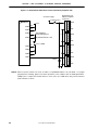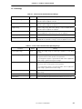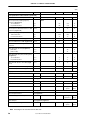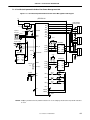
1
User’s Manual
TM
ECOUSB
Series
μPD720114
USB 2.0 Hub Controller
Document No. S17463EJ5V0UD00 (5th edition)
Date Published January 2008 NS
2005
Printed in Japan
[MEMO]
2
User’s Manual S17463EJ5V0UD
NOTES FOR CMOS DEVICES
1
VOLTAGE APPLICATION WAVEFORM AT INPUT PIN
Waveform distortion due to input noise or a reflected wave may cause malfunction. If the input of the
CMOS device stays in the area between VIL (MAX) and VIH (MIN) due to noise, etc., the device may
malfunction. Take care to prevent chattering noise from entering the device when the input level is fixed,
and also in the transition period when the input level passes through the area between VIL (MAX) and
VIH (MIN).
2
HANDLING OF UNUSED INPUT PINS
Unconnected CMOS device inputs can be cause of malfunction. If an input pin is unconnected, it is
possible that an internal input level may be generated due to noise, etc., causing malfunction. CMOS
devices behave differently than Bipolar or NMOS devices. Input levels of CMOS devices must be fixed
high or low by using pull-up or pull-down circuitry. Each unused pin should be connected to VDD or GND
via a resistor if there is a possibility that it will be an output pin. All handling related to unused pins must
be judged separately for each device and according to related specifications governing the device.
3
PRECAUTION AGAINST ESD
A strong electric field, when exposed to a MOS device, can cause destruction of the gate oxide and
ultimately degrade the device operation. Steps must be taken to stop generation of static electricity as
much as possible, and quickly dissipate it when it has occurred.
Environmental control must be
adequate. When it is dry, a humidifier should be used. It is recommended to avoid using insulators that
easily build up static electricity. Semiconductor devices must be stored and transported in an anti-static
container, static shielding bag or conductive material. All test and measurement tools including work
benches and floors should be grounded.
The operator should be grounded using a wrist strap.
Semiconductor devices must not be touched with bare hands. Similar precautions need to be taken for
PW boards with mounted semiconductor devices.
4
STATUS BEFORE INITIALIZATION
Power-on does not necessarily define the initial status of a MOS device. Immediately after the power
source is turned ON, devices with reset functions have not yet been initialized. Hence, power-on does
not guarantee output pin levels, I/O settings or contents of registers. A device is not initialized until the
reset signal is received. A reset operation must be executed immediately after power-on for devices
with reset functions.
5
POWER ON/OFF SEQUENCE
In the case of a device that uses different power supplies for the internal operation and external
interface, as a rule, switch on the external power supply after switching on the internal power supply.
When switching the power supply off, as a rule, switch off the external power supply and then the
internal power supply. Use of the reverse power on/off sequences may result in the application of an
overvoltage to the internal elements of the device, causing malfunction and degradation of internal
elements due to the passage of an abnormal current.
The correct power on/off sequence must be judged separately for each device and according to related
specifications governing the device.
6
INPUT OF SIGNAL DURING POWER OFF STATE
Do not input signals or an I/O pull-up power supply while the device is not powered. The current
injection that results from input of such a signal or I/O pull-up power supply may cause malfunction and
the abnormal current that passes in the device at this time may cause degradation of internal elements.
Input of signals during the power off state must be judged separately for each device and according to
related specifications governing the device.
User’s Manual S17463EJ5V0UD
3
ECOUSB is a trademark of NEC Electronics Corporation.
• The information in this document is current as of January, 2008. The information is subject to
change without notice. For actual design-in, refer to the latest publications of NEC Electronics data
sheets or data books, etc., for the most up-to-date specifications of NEC Electronics products. Not
all products and/or types are available in every country. Please check with an NEC Electronics sales
representative for availability and additional information.
• No part of this document may be copied or reproduced in any form or by any means without the prior
written consent of NEC Electronics. NEC Electronics assumes no responsibility for any errors that may
appear in this document.
• NEC Electronics does not assume any liability for infringement of patents, copyrights or other intellectual
property rights of third parties by or arising from the use of NEC Electronics products listed in this document
or any other liability arising from the use of such products. No license, express, implied or otherwise, is
granted under any patents, copyrights or other intellectual property rights of NEC Electronics or others.
• Descriptions of circuits, software and other related information in this document are provided for illustrative
purposes in semiconductor product operation and application examples. The incorporation of these
circuits, software and information in the design of a customer's equipment shall be done under the full
responsibility of the customer. NEC Electronics assumes no responsibility for any losses incurred by
customers or third parties arising from the use of these circuits, software and information.
• While NEC Electronics endeavors to enhance the quality, reliability and safety of NEC Electronics products,
customers agree and acknowledge that the possibility of defects thereof cannot be eliminated entirely. To
minimize risks of damage to property or injury (including death) to persons arising from defects in NEC
Electronics products, customers must incorporate sufficient safety measures in their design, such as
redundancy, fire-containment and anti-failure features.
• NEC Electronics products are classified into the following three quality grades: "Standard", "Special" and
"Specific".
The "Specific" quality grade applies only to NEC Electronics products developed based on a customerdesignated "quality assurance program" for a specific application. The recommended applications of an NEC
Electronics product depend on its quality grade, as indicated below. Customers must check the quality grade of
each NEC Electronics product before using it in a particular application.
"Standard": Computers, office equipment, communications equipment, test and measurement equipment, audio
and visual equipment, home electronic appliances, machine tools, personal electronic equipment
and industrial robots.
"Special": Transportation equipment (automobiles, trains, ships, etc.), traffic control systems, anti-disaster
systems, anti-crime systems, safety equipment and medical equipment (not specifically designed
for life support).
"Specific": Aircraft, aerospace equipment, submersible repeaters, nuclear reactor control systems, life
support systems and medical equipment for life support, etc.
The quality grade of NEC Electronics products is "Standard" unless otherwise expressly specified in NEC
Electronics data sheets or data books, etc. If customers wish to use NEC Electronics products in applications
not intended by NEC Electronics, they must contact an NEC Electronics sales representative in advance to
determine NEC Electronics' willingness to support a given application.
(Note)
(1) "NEC Electronics" as used in this statement means NEC Electronics Corporation and also includes its
majority-owned subsidiaries.
(2) "NEC Electronics products" means any product developed or manufactured by or for NEC Electronics (as
defined above).
M8E 02. 11-1
4
User’s Manual S17463EJ5V0UD
Major Revisions in this Edition
Page
p. 48
Description
Change of Table 6-4. Absolute Maximum Ratings
The mark <R> shows major revised points.
The revised points can be easily searched by copying an "<R>" in the PDF file and specifying it in the "Find what:" field.
User’s Manual S17463EJ5V0UD
5
PREFACE
Readers
This manual is intended for engineers who need to be familiar with the capability of
the μPD720114 in order to develop application systems based on it.
Purpose
The purpose of this manual is to help users understand the hardware capabilities
(listed below) of the μPD720114.
Configuration
This manual consists of the following chapters:
• Introduction
• Pin functions
• Descriptors information
• USB requests information
• How to connect to external discrete components
• Product specifications
• Application information
Guidance
Readers of this manual should already have a general knowledge of electronics, logic
circuits, and microcomputers.
Notation
This manual uses the following conventions:
Data bit significance:
High-order bits on the left side;
low-order bits on the right side
Active low:
XXXXB (Pin and signal names are suffixed with B.)
Note:
Explanation of an indicated part of text
Caution:
Information requiring the user’s special attention
Remark:
Supplementary information
Numerical value:
Binary ... xxxx or xxxxb
Decimal ... xxxx
Hexadecimal ... xxxxh
Related Document
Use this manual in combination with the following document.
The related documents indicated in this publication may include preliminary versions.
However, preliminary versions are not marked as such.
μPD720114 Data Sheet: S17462E
6
User’s Manual S17463EJ5V0UD
CONTENTS
CHAPTER 1 INTRODUCTION ................................................................................................................ 11
1.1
1.2
1.3
1.4
1.5
Features .................................................................................................................................... 11
Ordering Information ............................................................................................................... 11
Block Diagram .......................................................................................................................... 12
Pin Configuration (Top View).................................................................................................. 14
in Information ........................................................................................................................... 16
CHAPTER 2 PIN FUNCTIONS............................................................................................................... 17
2.1
2.2
2.3
2.4
2.5
2.6
2.7
Power Supply ........................................................................................................................... 17
Analog Signaling...................................................................................................................... 17
System Clock & Reset ............................................................................................................. 17
USB Hub Interface ................................................................................................................... 18
USB Interface............................................................................................................................ 19
System Interface ...................................................................................................................... 19
Test Signals .............................................................................................................................. 19
CHAPTER 3 DESCRIPTORS INFORMATION ...................................................................................... 20
3.1
3.2
3.3
3.4
3.5
3.6
3.7
3.8
Device Descriptor .................................................................................................................... 20
Device_Qualifier descriptor .................................................................................................... 21
Configuration descriptor......................................................................................................... 21
Interface descriptor ................................................................................................................. 22
Endpoint descriptor................................................................................................................. 22
Other_Speed_Configuration descriptor ................................................................................ 23
String descriptors .................................................................................................................... 23
Class Specified – Hub Class Descriptor................................................................................ 24
CHAPTER 4 USB REQUESTS INFORMATION................................................................................... 25
4.1
4.2
4.3
4.4
4.5
4.6
Standard Requests .................................................................................................................. 25
Class-Specific Requests ......................................................................................................... 27
The Response for Each Transaction ..................................................................................... 29
Hub Status Field and Hub Change Field ............................................................................... 34
Port Status Field and Port Change Field ............................................................................... 35
PORT_INDICATOR ................................................................................................................... 37
CHAPTER 5 HOW TO CONNECT TO EXTERNAL DISCRETE COMPONENTS ........................... 40
5.1
5.2
5.3
5.4
5.5
5.6
5.7
USB Upstream Port Connection............................................................................................. 40
USB Downstream Port Connection........................................................................................ 40
Power Switching Connection ................................................................................................. 41
LED Connection ....................................................................................................................... 43
Crystal Connection .................................................................................................................. 44
RREF and Internal Regulator Connection ............................................................................. 45
Handling Unused Pins............................................................................................................. 45
User’s Manual S17463EJ5V0UD
7
CHAPTER 6 PRODUCT SPECIFICATIONS.......................................................................................... 46
6.1
6.2
6.3
6.4
6.5
6.6
6.7
6.8
Buffer List ................................................................................................................................. 46
Terminology.............................................................................................................................. 47
Absolute Maximum Ratings .................................................................................................... 48
Recommended Operating Ranges ......................................................................................... 49
DC Characteristics ................................................................................................................... 50
Power Consumption ................................................................................................................ 54
AC Characteristics ................................................................................................................... 55
Timing Diagram ........................................................................................................................ 62
CHAPTER 7 APPLICATION INFORMATION ........................................................................................ 66
7.1
7.2
7.3
7.4
8
4 Port Self-powered Individual Port Power Management Hub ............................................ 66
3 Port Bus/self-powered Individual Port Power Management Hub..................................... 67
4 Port Self-powered Ganged Port Power Management Hub................................................ 68
2 Port Hub with One Embedded Device................................................................................. 69
User’s Manual S17463EJ5V0UD
LIST OF FIGURES
Figure No.
Title
Page
4-1
Port Indicator State Diagram ......................................................................................................................... 37
5-1
USB Upstream Port Connection .................................................................................................................... 40
5-2
USB Downstream Port Connection................................................................................................................ 40
5-3
Individual Port Power Switching and Individual Port Over-current Protection................................................ 41
5-4
Self-powered, Global Over-current Protection by Polymeric PTC ................................................................. 42
5-5
LED Connection............................................................................................................................................. 43
5-6
Crystal Connection ........................................................................................................................................ 44
5-7
RREF and Internal Regulator Connection ..................................................................................................... 45
6-1
Differential Input Sensitivity Range for Low-/full-speed.................................................................................. 52
6-2
Full-speed Buffer VOH/IOH Characteristics for High-speed Capable Transceiver ........................................ 52
6-3
Full-speed Buffer VOL/IOL Characteristics for High-speed Capable Transceiver ......................................... 52
6-4
Receiver Sensitivity for Transceiver at DP/DM .............................................................................................. 53
6-5
Receiver Measurement Fixtures .................................................................................................................... 53
6-6
System Reset Timing..................................................................................................................................... 55
6-7
Over-current Response Timing...................................................................................................................... 56
6-8
CSB/PPB Timing ........................................................................................................................................... 56
6-9
Transmit Waveform for Transceiver at DP/DM .............................................................................................. 61
6-10
Transmitter Measurement Fixtures ................................................................................................................ 61
6-11
Hub Differential Delay, Differential Jitter, and SOP Distortion ....................................................................... 62
6-12
Hub EOP Delay and EOP Skew .................................................................................................................... 63
6-13
USB Differential Data Jitter for Low-/full-speed ............................................................................................. 64
6-14
USB Differential-to-EOP Transition Skew and EOP Width for Low-/full-speed.............................................. 64
6-15
USB Receiver Jitter Tolerance for Low-/full-speed ........................................................................................ 64
6-16
Low-/full-speed Disconnect Detection............................................................................................................ 65
6-17
Full-/high-speed Device Connect Detection................................................................................................... 65
6-18
Power-on and Connection Events Timing...................................................................................................... 65
7-1
4 Port Self-powered Individual Port Power Management Hub with LED Indicator Diagram .......................... 66
7-2
3 Port Bus/self-powered Individual Port Power Management Hub Diagram.................................................. 67
7-3
4 Port Self-powered Ganged Port Power Management Hub without LED Indicator Diagram........................ 68
7-4
2 Port Hub with Embedded Device Diagram ................................................................................................. 69
User’s Manual S17463EJ5V0UD
9
LIST OF TABLES
Table No.
Title
Page
4-1
Hub Status Field, wHubStatus .......................................................................................................................34
4-2
Hub Change Field, wHubChange ..................................................................................................................34
4-3
Port Status Field, wPortStatus .......................................................................................................................35
4-4
Port Change Field, wPortChange ..................................................................................................................36
4-5
Indicator Colors and Port Status ....................................................................................................................38
4-6
Port Indicator Selectors..................................................................................................................................38
5-1
External Parameters ......................................................................................................................................44
6-1
Terms Used in Absolute Maximum Ratings ...................................................................................................47
6-2
Terms Used in Recommended Operating Range ..........................................................................................47
6-3
Terms Used in DC Characteristics.................................................................................................................48
6-4
Absolute Maximum Ratings ...........................................................................................................................48
6-5
Recommended Operating Ranges ................................................................................................................49
6-6
DC Characteristics (Control Pin Block) ..........................................................................................................50
6-7
DC Characteristics (USB Interface Block)......................................................................................................51
6-8
Power Consumption.......................................................................................................................................54
6-9
Pin capacitance .............................................................................................................................................55
6-10
System Clock Specification............................................................................................................................55
6-11
System Reset Signaling.................................................................................................................................55
6-12
AC Characteristics (Over-current Response Timing) .....................................................................................56
6-13
AC Characteristics (USB Interface Block)......................................................................................................57
10
User’s Manual S17463EJ5V0UD
CHAPTER 1 INTRODUCTION
The μPD720114 is a USB 2.0 hub device that complies with the Universal Serial Bus (USB) Specification Revision
2.0 and works up to 480 Mbps. USB2.0 compliant transceivers are integrated for upstream and all downstream ports.
The μPD720114 works backward compatible either when any one of the downstream ports is connected to a USB 1.1
compliant device, or when the upstream port is connected to a USB 1.1 compliant host.
1.1 Features
• Compliant with Universal Serial Bus Specification Revision 2.0 (Data Rate 1.5/12/480 Mbps)
• High-speed or full-speed packet protocol sequencer for Endpoint 0/1
• 4 (Max.) downstream facing ports
• Low power consumption (10 μA when hub in idle status, 149 mA when all parts run in HS mode)
• All downstream facing ports can handle high-speed (480 Mbps), full-speed (12 Mbps), and low-speed (1.5
Mbps) transaction.
• Supports split transaction to handle full-speed and low-speed transaction on downstream facing ports when
Hub controller is working in high-speed mode.
• One Transaction Translator per Hub and supports four non-periodic buffers
• Supports self-powered and bus-powered mode
• Supports individual or global over-current detection and individual or ganged power control
• Supports downstream port status with LED
• Supports non-removable devices by I/O pin configuration
• Support Energy Star for PC peripheral system
• On chip Rpu, Rpd resistors and regulator (for core logic)
• Use 30 MHz crystal
• 3.3 V power supply
1.2 Ordering Information
Part Number
Package
Remark
μPD720114GA-9EU-A
48-pin plastic TQFP (Fine pitch) (7 × 7)
Lead-free product
μPD720114GA-YEU-A
48-pin plastic TQFP (Fine pitch) (7 × 7)
Lead-free product
User’s Manual S17463EJ5V0UD
11
CHAPTER 1 INTRODUCTION
1.3 Block Diagram
To Host/Hub
downstream
facing port
Upstream facing port
UP_PHY
CDR
SERDES
UPC
FS_REP
SIE_2H
CDR
ALL_TT
F_TIM
EP1
DP(1)_PHY
Downstream facing port #1
EP0
DP(2)_PHY
Downstream facing port #2
APLL
DP(3)_PHY
Downstream facing port #3
X1/X2
OSB
DP(4)_PHY
Downstream facing port #4
2.5V REG
12
User’s Manual S17463EJ5V0UD
To Hub/Function
upstream facing port
To Hub/Function
upstream facing port
To Hub/Function
upstream facing port
To Hub/Function
upstream facing port
CHAPTER 1 INTRODUCTION
APLL
: Generates all clocks of Hub.
ALL_TT
: Translates the high-speed transactions (split transactions) for full/low-speed device
to full/low-speed transactions.
ALL_TT buffers the data transfer from either
upstream or downstream direction. For OUT transaction, ALL_TT buffers data from
upstream port and sends it out to the downstream facing ports after speed
conversion from high-speed to full/low-speed. For IN transaction, ALL_TT buffers
data from downstream ports and sends it out to the upstream facing ports after
speed conversion from full/low-speed to high-speed.
CDR
: Data & clock recovery circuit
DPC
: Downstream Port Controller handles Port Reset, Enable, Disable, Suspend and
DP(n)_PHY
: Downstream transceiver supports high-speed (480 Mbps), full-speed (12 Mbps), and
EP0
: Endpoint 0 controller
EP1
: Endpoint 1 controller
F_TIM (Frame Timer)
: Manages hub’s synchronization by using micro-SOF which is received at upstream
Resume
low-speed (1.5 Mbps) transaction
port, and generates SOF packet when full/low-speed device is attached to
downstream facing port.
FS_REP
: Full/low-speed repeater is enabled when the μPD720114 is worked at full-speed
mode
OSB
: Oscillator Block
2.5V REG
: On chip 2.5V regulator
SERDES
: Serializer and Deserializer
SIE_2H
: Serial Interface Engine (SIE) controls USB2.0 and 1.1 protocol sequencer.
UP_PHY
: Upstream Transceiver supports high-speed (480 Mbps), full-speed (12 Mbps)
transaction
UPC
: Upstream Port Controller handles Suspend and Resume
User’s Manual S17463EJ5V0UD
13
CHAPTER 1 INTRODUCTION
1.4 Pin Configuration (Top View)
• 48-pin plastic TQFP (Fine pitch) (7 × 7)
VDD33REG
VBUSM
CSB1
PPB1
CSB2
PPB2
VSS
CSB3
PPB3
CSB4
PPB4
SYSRSTB
μPD720114GA-9EU-A
μPD720114GA-YEU-A
48 47 46 45 44 43 42 41 40 39 38 37
VDD25OUT
VSSREG
LED4
LED3
LED2
LED1
GREEN
AMBER
VDD33
X1
X2
VDD25
36
35
34
33
32
31
30
29
28
27
26
25
1
2
3
4
5
6
7
8
9
10
11
12
BUS_B
TEST
RREF
AVSS(R)
AVDD
AVSS
AVDD
VDD33
DMU
DPU
VSS
VDD25
13 14 15 16 17 18 19 20 21 22 23 24
14
User’s Manual S17463EJ5V0UD
VSS
DP4
DM4
VDD25
DP3
DM3
VDD33
DP2
DM2
VSS
DP1
DM1
CHAPTER 1 INTRODUCTION
Pin No.
Pin Name
Pin No.
Pin Name
Pin No.
Pin Name
Pin No.
Pin Name
1
VDD25OUT
13
BUS_B
25
DM1
37
SYSRSTB
2
VSSREG
14
TEST
26
DP1
38
PPB4
3
LED4
15
RREF
27
VSS
39
CSB4
4
LED3
16
AVSS(R)
28
DM2
40
PPB3
5
LED2
17
AVDD
29
DP2
41
CSB3
6
LED1
18
AVSS
30
VDD33
42
VSS
7
GREEN
19
AVDD
31
DM3
43
PPB2
8
AMBER
20
VDD33
32
DP3
44
CSB2
9
VDD33
21
DMU
33
VDD25
45
PPB1
10
X1
22
DPU
34
DM4
46
CSB1
11
X2
23
VSS
35
DP4
47
VBUSM
12
VDD25
24
VDD25
36
VSS
48
VDD33REG
Remark AVSS(R) should be used to connect RREF through 1 % precision reference resistor of 2.43 kΩ.
User’s Manual S17463EJ5V0UD
15
CHAPTER 1 INTRODUCTION
1.5 Pin Information
Pin Name
I/O
Buffer Type
Active
Function
Level
X1
I
2.5 V input
30 MHz crystal oscillator in
X2
O
2.5 V output
30 MHz crystal oscillator out
SYSRSTB
I
3.3 V Schmitt input
DP(4:1)
I/O
USB D+ signal I/O
USB’s downstream facing port D+ signal
DM(4:1)
I/O
USB D− signal I/O
USB’s downstream facing port D− signal
DPU
I/O
USB D+ signal I/O
USB’s upstream facing port D+ signal
DMU
I/O
USB D− signal I/O
USB’s upstream facing port D− signal
BUS_B
I
3.3 V Schmitt input
Power mode select
RREF
A (O)
Analog
Reference resistor connection
CSB1
I
5 V tolerant Schmitt input
Low
Port’s over-current status input
CSB(4:2)
I
3.3 V Schmitt input
Low
Port’s over-current status input
PPB(4:1)
I/O
3.3 V output/input
Low
Low
Asynchronous chip hardware reset
Port’s power supply control output or hub
configuration input
VBUSM
I
AMBER
I/O
5 V tolerant Schmitt input
Upstream VBUS monitor
3.3V output/input
Amber colored LED control output or port
indicator select
GREEN
O
3.3V output
Green colored LED control output or port
indicator select
LED(4:1)
I/O
3.3V output/input
Low
LED indicator output show downstream port
status or Removable/Non-removable select
TEST
I
3.3 V Schmitt input
VDD25OUT
Test signal
On chip 2.5 V output, supply the VDD25 for the chip
self, it must have a 22 μF (or greater) capacitor to
VSSREG.
VDD33
3.3 V VDD
VDD33REG
3.3 V VDD for on chip 2.5 V regulator input, it must
have a 4.7 μF (or greater) capacitor to VSSREG
VDD25
2.5 V VDD, These pins must be supplied from
VDD25OUT, output from internal regulator
AVDD
2.5 V VDD for analog circuit
VSS
VSS
VSSREG
On chip 2.5 V regulator VSS
AVSS
VSS for analog circuit
AVSS(R)
VSS for reference resistor, Connect to AVSS.
Remark “5 V tolerant“ means that the buffer is 3 V buffer with 5 V tolerant circuit.
16
User’s Manual S17463EJ5V0UD
CHAPTER 2 PIN FUNCTIONS
The pin type describes a signal either as analog, power, input, or I/O (bi-directional).
2.1 Power Supply
Pin
Pin No.
Direction
Function
VDD33
9, 20, 30
Power
+3.3 V power supply
VDD33REG
48
Power
+3.3 V power supply for on chip 2.5 V regulator input, it must have a
4.7 μF (or greater) capacitor to VSSREG.
VDD25
12, 24, 33
Power
+2.5 V core power line, it must have a 0.1 μF (or greater) capacitor to
VSS. These pins must be supplied from VDD25OUT, output from internal
regulator
VDD25OUT
1
Power
On chip 2.5 V output, supply the VDD25 for the chip self, it must have a
22 μF (or greater) capacitor to VSSREG.
AVDD
17, 19
Power
+2.5 V analog circuit power line, it must have a 0.1 μF (or greater)
capacitor to VSS.
VSS
23, 27, 36, 42
Power
Ground
VSSREG
2
Power
Ground for on chip 2.5 V regulator
AVSS
18
Power
Ground for analog circuit
AVSS(R)
16
Power
Ground for reference resistor
Remark
Self-Powered Hub System requires the capability of providing 500 mA for each downstream facing
port. And additional power consumption of Hub Controller itself and other components in the Hub
System should also be considered for overall power requirement. A power source that is able to
supply at least 2.5 A may be best for a 4 port Self-Powered Hub System.
2.2 Analog Signaling
Pin
RREF
Pin No.
15
Direction
Analog
Function
RREF must be connected a 1 % precision reference resistor of 2.43
kΩ. The other side of the resistor must be connected to AVSS(R) which
must then it must be connected to AVSS.
2.3 System Clock & Reset
Pin
Pin No.
Direction
Function
X1
10
I
Oscillator crystal input. Connect to 30-MHz crystal
X2
11
O
Oscillator crystal output. Connect through a series resistor to other end
of 30-MHz crystal.
SYSRSTB
37
I
Asynchronous active low reset signal
User’s Manual S17463EJ5V0UD
17
CHAPTER 2 PIN FUNCTIONS
2.4 USB Hub Interface
Pin
CSB(4:1)
Pin No.
Direction
39, 41, 44, 46
I
Function
Over-current status input of the downstream facing ports.
1: No over-current condition detected.
0: Over-current condition detected.
If the pin is not used, connect to GND or VDD33.
PPB(4:1)
38, 40, 43, 45
I/O
Power supply control output for downstream facing ports (open-drain).
1: Power supply OFF
0: Power supply ON
By strapping PPB(4:1) pins before system reset (see Chapter 5 and 7),
the active ports, power management mode and bPwrOn2PwrGood
descriptor can configure as bellow:
PPB [4:3] = 00: 2 downstream facing ports active.
= 01: 3 downstream facing ports active
= 11: 4 downstream facing ports active
PPB2 = 0: ganged power management mode
=1: individual power management mode
PPB1 = 0: bPwrOn2PwrGood = 00h(0 ms, with no power switches)
= 1: bPwrOn2PwrGood = 32h(100 ms)
VBUSM
47
LED(4:1)
3, 4, 5, 6
I
I/O
Upstream Vbus monitor.
Connect to downstream facing port status indicator LED (open drain).
See Figure 5-5. LED Connection.
If port indicator is not used, connect GREEN to AMBER directly. The
LED(4:1) can configure for removable/non-removable selection:
0: Removable
1: Non-removable
AMBER
8
I/O
Connect to amber colored LED. See Figure 5-5. LED Connection.
The meaning of amber colored LED is described in section
4.6 PORT_INDICATOR.
If port indicator is not used, connect it to GREEN directly.
GREEN
7
O
Connect to green colored LED. See Figure 5-5. LED Connection.
The meaning of green colored LED is described in section
4.6 PORT_INDICATOR.
If port indicator is not used, connect it to AMBER directly.
Remark VBUSM pin may be used to monitor the VBUS line even if VDD33 is shut off. For example, the internal
Rpu for the DPU pin is powered by VBUSM for port speed indication. The input voltage level for
VBUSM pin should be less than 3.3 V in order not to exceed the absolute maximum rating. Refer to
Figure 5-1. USB Upstream Port Connection and use voltage divider resistors to monitor VBUS.
18
User’s Manual S17463EJ5V0UD
CHAPTER 2 PIN FUNCTIONS
2.5 USB Interface
Pin
DP(4:1)
Pin No.
Direction
35, 32, 29, 26
I/O
Function
Connect to downstream port D+ signal line.
If not using the downstream port, connect to GND.
DM(4:1)
34, 31, 28, 25
I/O
Connect to downstream port D− signal line.
If not using the downstream port, connect to GND.
DPU
22
I/O
Connect to upstream facing port D+ signal line.
DMU
21
I/O
Connect to upstream facing port D− signal line.
2.6 System Interface
Pin
BUS_B
Pin No.
13
Direction
I
Function
Select power mode
0: Bus-powered
1: Self-powered
2.7 Test Signals
Pin
TEST
Pin No.
14
Direction
I
Caution
Should be tied to GND on circuit board.
User’s Manual S17463EJ5V0UD
19
CHAPTER 3 DESCRIPTORS INFORMATION
This chapter describes the descriptors implemented in hub controller. The μPD720114 has following descriptors.
Host reads these descriptors by using Get Descriptor request.
•
Device Descriptor
•
Device Qualifier Descriptor
•
Configuration Descriptor
•
Interface Descriptor
•
Endpoint Descriptor
•
Other Speed Configuration Descriptor
•
Hub Class-specific Descriptor
The hub returns different descriptors depending on whether it is operating at high-speed or full-speed.
following section shows descriptor sets for full-speed operation and high-speed operation.
3.1 Device Descriptor
The hub returns Device descriptor by GET_DESCRIPTOR (Device) request.
Offset
Field Name
Full-speed
High-speed
Description
0
bLength
12h
12h
1
bDescriptorType
01h
01h
2
bcdUSB
0200h
0200h
USB specification 2.0
4
bDeviceClass
09h
09h
Hub
5
bDeviceSubClass
00h
00h
6
bDeviceProtocol
00h
01h
Single TT for high-speed
7
bMxPacketSize0
40h
40h
64 bytes
8
idVendor
0409h
0409h
"NEC"
10
idProduct
005Ah
005Ah
"USB 2.0 Hub Controller"
12
bcdDevice
0100h
0100h
"1.00"
14
iManufacturer
00h
00h
15
iProduct
00h
00h
16
iSerialNumber
00h
00h
17
bNumConfigurations
01h
01h
20
18 bytes
One configuration
User’s Manual S17463EJ5V0UD
The
CHAPTER 3 DESCRIPTORS INFORMATION
3.2 Device_Qualifier descriptor
The hub returns Device_Qualifier descriptor by GET_DESCRIPTOR (Device_Qualifier) request.
Offset
Field Name
Full-speed
High-speed
Description
0
bLength
0Ah
0Ah
10 bytes
1
bDescriptorType
06h
06h
2
bcdUSB
0200h
0200h
USB specification 2.0
4
bDeviceClass
09h
09h
Hub
5
bDeviceSubClass
00h
00h
6
bDeviceProtocol
01h
00h
Single TT for high-speed
7
bMaxPacketSize0
40h
40h
64 bytes
8
bNumConfigurations
01h
01h
9
bReserved
00h
00h
3.3 Configuration descriptor
The hub returns Configuration descriptor by GET_DESCRIPTOR (Configuration) request.
Offset
Field Name
Full-speed
High-speed
Description
0
bLength
09h
09h
9 bytes
1
bDescriptorType
02h
02h
2
wTotalLength
0019h
0019h
25 bytes
4
bNumInterfaces
01h
01h
One interface
5
bConfigurationValue
01h
01h
6
iConfiguration
00h
00h
7
bmAttributes
E0h
E0h
8
bMaxPower
32h
32h
100 mA
User’s Manual S17463EJ5V0UD
21
CHAPTER 3 DESCRIPTORS INFORMATION
3.4 Interface descriptor
The hub returns Configuration descriptor followed by Interface descriptor.
Offset
Field Name
Full-speed
High-speed
0
bLength
09h
09h
1
bDescriptorType
04h
04h
2
bInterfaceNumber
00h
00h
3
bAlternateSetting
00h
00h
4
bNumEndpoints
01h
01h
5
bInterfaceClass
09h
09h
6
bInterfaceSubClass
00h
00h
7
bInterfaceProtocol
00h
00h
8
iInterface
00h
00h
Description
9 bytes
3.5 Endpoint descriptor
The hub returns Configuration/Interface descriptor followed by Endpoint descriptor.
Offset
Field Name
Full-speed
High-speed
Description
0
bLength
07h
07h
1
bDescriptorType
05h
05h
2
bEndpointAddress
81h
81h
EP1, IN direction
3
bmAttributes
03h
03h
Interrupt endpoint
4
wMaxPacketSize
0001h
0001h
1 byte
6
bInterval
FFh
0Ch
Polling interval
22
7 bytes
User’s Manual S17463EJ5V0UD
CHAPTER 3 DESCRIPTORS INFORMATION
3.6 Other_Speed_Configuration descriptor
The hub returns Other_Speed_Configuration descriptor by GET_DESCRIPTOR (Other_Speed_Configuration)
request.
Offset
Field Name
Full-speed
High-speed
0
bLength
09h
09h
1
bDescriptorType
07h
07h
2
wTotalLength
0019h
0019h
4
bNumInterfaces
01h
01h
5
bConfigurationValue
01h
01h
6
iConfiguration
00h
00h
7
bmAttributes
E0h
E0h
8
bMaxPower
32h
32h
Description
9 bytes
25 bytes
100 mA
3.7 String descriptors
The μPD720114 doesn’t support string descriptors, it will return “STALL” by GET_DESCRIPTOR (string) request.
User’s Manual S17463EJ5V0UD
23
CHAPTER 3 DESCRIPTORS INFORMATION
3.8 Class Specified – Hub Class Descriptor
The hub returns Hub Class descriptors by GetHubDescriptor request.
Offset
Field Name
Value
Description
0
bDescLength
09h
9 bytes
1
bDescriptorType
29h
Hub
2
bNbrPorts
3
5
wHubCharacteristics
bPwrOn2PwrGood
Pin configuration
04h
4 downstream facing ports
PPB [4:3] = 11
03h
02h
3 downstream facing ports
2 downstream facing ports
PPB [4:3] = 01
PPB [4:3] = 00
01b (D1:D0)
00b (D1:D0)
Individual port power switching
Ganged power switching
PPB2 = 1
PPB2 = 0
0b (D2)
1b (D2)
Not compound device
Compound device
All LEDx = 0
01b (D4:D3)
Individual port over-current
PPB2 = 1
00b (D4:D3)
protection
Global over-current protection
PPB2 = 0
01b (D6:D5)
TT Think Time is 16 FS bit time
1b (D7)
Support PORT_INDICATOR
LED connected
0b
PORT_INDICATOR not support
GREEN = AMBER
32h
100 ms
PPB1 = 1
00h
0 ms
PPB1 = 0
Any LEDx = 1
6
bHubContrCurrent
64h
Hub’s current is “100 mA”
7
DeviceRemovable
0b
Reserved
0b (D1)
Device is removable
LED1 = 0
1b (D1)
Device is not removable
LED1 = 1
0b (D2)
1b (D2)
Device is removable
Device is not removable
LED2 = 0
0b (D3)
1b (D3)
Device is removable
Device is not removable
0b (D4)
1b (D4)
Device is removable
Device is not removable
8
PortPwrCtrlMask
Note 1
Note 2
Note 3
Note 1
Note 1
LED2 = 1
LED3 = 0
Note 1
LED3 = 1
LED4 = 0
Note 1
LED4 = 1
FFh
Notes 1. When port indicator is not used, connect GREEN to AMBER directly and the LED(4:1) can configure for
removable/non-removable selection. Else if port indicator is used, connect LED with Figure 5-5, the
downstream facing port of μPD720114 will be fixed at removable.
2. When LEDs are connected (see Figure 5-5), μPD720114 will report D7 of wHubCharacteristics with
“1b” to host PC. Else if LEDs are not used, connect GREEN to AMBER directly; μPD720114 will report
D7 of wHubCharacteristics with “0b” to host PC.
3. Bus-powered hub requires power switches. PPBx are for power switch control (see Figure 5-3). For low
BOM cost self-powered hub design with no power switches (over current protection by polymeric PTC
for logical power switching mode), set PPB2 = PPB1 = 0 (see Figure 5-4), bPwrOn2PwrGood is set at 0.
It complies with the USB Specification.
24
User’s Manual S17463EJ5V0UD
CHAPTER 4 USB REQUESTS INFORMATION
When the μPD720114 is connected to a downstream facing port of a USB2.0 host controller or USB2.0 Hub, it
operates in high-speed mode on the upstream facing port. The μPD720114 uses USB2.0 high-speed protocols to
communicate with other USB2.0 devices. On the other hand, when the μPD720114 is connected to a downstream
facing port of a USB1.x host controller or USB1.x Hub, it operates in full-speed mode. The μPD720114 uses USB2.0
full-speed protocols to communicate with the upstream controller.
•
Handles setup transactions for Endpoint 0 which are controlled by the hub itself.
•
Repeats setup transactions to other devices.
•
Handles interrupt transactions for Endpoint 1 which retrieve status change information
•
Repeats interrupt transactions to other devices.
•
Repeats bulk transactions to other devices.
•
Repeats isochronous transactions to other devices.
•
Translates split transactions for USB1.X devices which are attached to the downstream facing port.
•
Repeats split transactions to a USB2.0 hub which is attached to the downstream facing port.
This section describes requests supported by the μPD720114 default descriptor setting. Please refer to Chapter 9
and 11 in the USB specification rev. 2.0 for further detail.
4.1 Standard Requests
The μPD720114 supports all standard requests except for SET_DESCRIPTOR() and SYNCH_FRAME(). The
following table shows the standard requests at the default setting.
(1/2)
Request
bmRequestType
bRequest
00000000b
01h
0001h
0000h
0000h
None
CLEAR_FEATURE (Endpoint 0
Halt)
00000010b
01h
0000h
0000h /
0080h
0000h
None
CLEAR_FEATURE (Endpoint 1
Halt)
00000010b
01h
0000h
0081h
0000h
None
GET_CONFIGURATION
10000000b
08h
0000h
0000h
0001h
CLEAR_FEATURE (Device:
wValue
wIndex
wLength
Return
Remote Wakeup)
GET_DESCRIPTOR (Device)
10000000b
06h
0100h
0000h
Current configuration value
0012h
Note
Device descriptor
Note
Configuration / Interface /
Endpoint descriptors
GET_DESCRIPTOR
(Configuration)
10000000b
06h
0200h
0000h
0019h
GET_DESCRIPTOR
(Device_Qualifier)
10000000b
06h
0600h
0000h
000Ah Note
Device_Qualifier
Note The wLength field specifies the number of bytes to return. If the data to be returned is longer than the
wLength field, only wLength bytes of the descriptor are returned. If the data to be returned is shorter than
the wLength field, the device ends the control transfer by sending a short packet when more data is
requested.
User’s Manual S17463EJ5V0UD
25
CHAPTER 4 USB REQUESTS INFORMATION
(2/2)
Request
GET_DESCRIPTOR
bmRequestType
10000000b
bRequest
06h
wValue
0700h
wIndex
0000h
wLength
0019h
Return
Other_Speed_Configuration
Note
(Other_Speed_Configuration)
GET_INTERFACE
10000001b
0Ah
0000h
0000h
0001h
00h
GET_STATUS (Device)
10000000b
00h
0000h
0000h
0002h
Device status
GET_STATUS (Interface)
10000001b
00h
0000h
0000h
0002h
0000h
GET_STATUS (Endpoint 0)
10000010b
00h
0000h
0000h/
0002h
Endpoint 0 status
0080h
GET_STATUS (Endpoint 1)
10000010b
00h
SET_ADDRESS
00000000b
05h
0000h
0081h
0002h
Endpoint 1 status
0000h to
0000h
0000h
None
0000h
0000h
None
0000h
0000h
None
0000h/
0000h
None
007Fh
SET_CONFIGURATION
00000000b
09h
0000h/
0001h
SET_FEATURE (Device: Remote
00000000b
03h
0001h
SET_FEATURE (Endpoint 0 Halt) 00000010b
03h
0000h
Wakeup)
0080h
SET_FEATURE (Endpoint 1 Halt) 00000010b
03h
0000h
0081h
0000h
None
SET_FEATURE (Test_J)
00000000b
03h
0002h
0100h
0000h
None
SET_FEATURE (Test_K)
00000000b
03h
0002h
0200h
0000h
None
SET_FEATURE (Test_SE0_NAK) 00000000b
03h
0002h
0300h
0000h
None
SET_FEATURE (Test_Packet)
00000000b
03h
0002h
0400h
0000h
None
SET_FEATURE
00000000b
03h
0002h
0500h
0000h
None
00000001b
0Bh
0000h
0000h
0000h
None
(Test_Force_Enable)
SET_INTERFACE
Note The wLength field specifies the number of bytes to return. If the data to be returned is longer than the
wLength field, only wLength bytes of the descriptor are returned. If the data to be returned is shorter than
the wLength field, the device ends the control transfer by sending a short packet when more data is
requested.
26
User’s Manual S17463EJ5V0UD
CHAPTER 4 USB REQUESTS INFORMATION
4.2 Class-Specific Requests
The μPD720114 supports all class-specific requests except for SetHubDescriptor() and GetBusState().
The
following table shows the class-specific requests at the default descriptor setting.
(1/2)
Request
ClearHubFeature (C_HUB_OVER
bmRequestType
bRequest
wValue
wIndex
wLength
Return
00100000b
01h
0001h
0000h
0000h
None
00100000b
01h
0000h
0000h
0000h
None
00100011b
01h
0001h
0001h to
0000h
None
0000h
None
0000h
None
_CURRENT)
ClearHubFeature (C_HUB_LOCAL
_POWER)
ClearPortFeature (PORT_ENABLE)
0004h
ClearPortFeature (PORT_SUSPEND)
00100011b
01h
0002h
0001h to
0004h
ClearPortFeature (PORT_POWER)
00100011b
01h
0008h
0001h to
0004h
ClearPortFeature (PORT_INDICATOR)
00100011b
01h
0016h
Note 1
0000h
None
ClearPortFeature
00100011b
01h
0010h
0001h to
0000h
None
0000h
None
0000h
None
0000h
None
0000h
None
(C_PORT_CONNECTION)
0004h
ClearPortFeature (C_PORT_RESET)
00100011b
01h
0014h
0001h to
0004h
ClearPortFeature (C_PORT_ENABLE)
00100011b
01h
0011h
0001h to
0004h
ClearPortFeature
00100011b
01h
0012h
(C_PORT_SUSPEND)
0001h to
0004h
ClearPortFeature
00100011b
01h
0013h
(C_PORT_OVER_CURRENT)
0001h to
0004h
GetHubDescriptor
10100000b
06h
2900h
0000h
0009h
GetHubStatus
10100000b
00h
0000h
0000h
0004h
Note 2
Hub descriptor
Hub status and
change indicators.
Refer to section 4.4.
Notes 1. The high byte of the wIndex field is the selector identifying the specific indicator. And the low byte of the
wIndex field shows port number. Refer to 4.6 PORT_INDICATOR for details.
Port Indicator Color
Port Indicator Mode
0h
Value
Default
Automatic
1h
Amber
Manual
2h
Green
3h
Off
4h to FFh
Reserved
Reserved
2. The wLength field specifies the number of bytes to return. If the data to be returned is longer than the
wLength field, only wLength bytes of the descriptor are returned. If the data to be returned is shorter
than the wLength field, the device ends the control transfer by sending a short packet when more data is
requested.
User’s Manual S17463EJ5V0UD
27
CHAPTER 4 USB REQUESTS INFORMATION
(2/2)
Request
GetPortStatus
bmRequestType
bRequest
wValue
10100011b
00h
0000h
wIndex
0001h to
wLength
0004h
0004h
Return
Port status and
change indicators.
Refer to section 4.5.
SetPortFeature (PORT_RESET)
00100011b
03h
0004h
0001h to
0004h
0000h
None
SetPortFeature (PORT_SUSPEND)
00100011b
03h
0002h
0001h to
0004h
0000h
None
SetPortFeature (PORT_POWER)
00100011b
03h
0008h
0001h to
0004h
0000h
None
SetPortFeature (PORT_TEST: Test_J)
00100011b
03h
0015h
0101h to
0104h
0000h
None
SetPortFeature (PORT_TEST: Test_K)
00100011b
03h
0015h
0201h to
0204h
0000h
None
SetPortFeature (PORT_TEST:
Test_SE0_NAK)
00100011b
03h
0015h
0301h to
0304h
0000h
None
SetPortFeature (PORT_TEST:
Test_Packet)
00100011b
03h
0015h
0401h to
0404h
0000h
None
SetPortFeature (PORT_TEST:
Test_Force_Enable)
00100011b
03h
0015h
0501h to
0504h
0000h
None
SetPortFeature (PORT_INDICATOR)
00100011b
03h
0016h
Note 1
0000h
None
ClearTTBuffer
00100011b
08h
Note 2
0001h
0000h
None
GetTTState
10100011b
0Ah
0000h
0001h
08D0h
TT state
ResetTT
00100011b
09h
0000h
0001h
0000h
None
StopTT
00100011b
0Bh
0000h
0001h
0000h
None
Notes 1. The high byte of the wIndex field is the selector identifying the specific indicator. And the low byte of the
wIndex field shows port number. Refer to 4.6 PORT_INDICATOR for details.
Port Indicator Color
Port Indicator Mode
0h
Value
Default
Automatic
1h
Amber
Manual
2h
Green
3h
Off
4h to FFh
Reserved
Reserved
2. The wValue for ClearTTBuffer is as follows.
Bits
28
Field
3..0
Endpoint Number
10..4
Device Address
12..11
Endpoint Type
14..13
Reserved, must be zero
15
Direction, 1 = IN, 0 = OUT
User’s Manual S17463EJ5V0UD
CHAPTER 4 USB REQUESTS INFORMATION
4.3 The Response for Each Transaction
USB specification rev. 2.0 states the device behavior in some states and conditions are not specified. The section
describes the response of the μPD720114 in each state and condition at default setting.
(1/2)
Request
Condition
Default state
Address state
Configured
Endpoint 0
Invalid
state
halted
wValue
Request accepted
Request accepted
Request accepted
STALL
Standard Requests
CLEAR_FEATURE
Device
STALL *
Endpoint 0
STALL *
Request accepted
Request accepted
Request accepted
STALL
Endpoint 1
STALL *
STALL
Request accepted
Request accepted
STALL
STALL *
Return data
Return data
STALL
STALL *
Device
Return data
Return data
Return data
STALL
STALL
Configuration
Return data
Return data
Return data
STALL
STALL
GET_CONFIGURATION
GET_DESCRIPTOR
Note
String
STALL
STALL
STALL
STALL
STALL
Device Qualifier
Return data
Return data
Return data
STALL
STALL
Other Speed Configuration
Return data
Return data
Return data
STALL
STALL
STALL *
STALL
Return data
STALL
STALL *
Device
STALL *
Return data
Return data
Return data
STALL *
Interface
STALL *
STALL
Return data
Return data
STALL *
Endpoint 0
STALL *
Return data
Return data
Return data
STALL *
Endpoint 1
STALL *
STALL
Return data
Return data
STALL *
SET_ADDRESS
Request accepted
Request accepted
STALL *
STALL
STALL *
SET_CONFIGURATION
STALL *
Request accepted
Request accepted
STALL
STALL *
STALL *
Request accepted
Request accepted
Request accepted
STALL
GET_INTERFACE
GET_STATUS
SET_FEATURE
Device
Endpoint 0
STALL *
Request accepted
Request accepted
Request accepted
STALL
Endpoint 1
STALL *
STALL
Request accepted
Request accepted
STALL
TEST_MODE in HS mode
Request accepted
Request accepted
Request accepted
Request accepted
STALL
TEST_MODE in FS mode
STALL
STALL
STALL
STALL
STALL
SET_INTERFACE
STALL *
STALL
Request accepted
STALL
STALL
Other Standard Requests
STALL
STALL
STALL
STALL
STALL
Note The wLength field specifies the number of bytes to return. If the data to be returned (or internal state of TT)
is longer than the wLength field, only wLength bytes of the data (or internal state of TT) are returned. If the
data to be returned (or internal state of TT) is shorter than the wLength field, the device ends the control
transfer by sending a short packet when more data is requested.
User’s Manual S17463EJ5V0UD
29
CHAPTER 4 USB REQUESTS INFORMATION
(2/2)
Request
Condition
Default state
Address state
Configured
Endpoint 0
Invalid
state
halted
wValue
Class-specific Requests
ClearHubFeature
C_HUB_LOCAL_POWER
No response *
No response *
Request accepted
Request accepted
STALL
C_HUB_OVER_CURRENT
No response *
No response *
Request accepted
Request accepted
STALL
No response *
No response *
Request accepted
Request accepted
STALL
Return data *
Return data *
Return data
Return data
STALL
No response *
No response *
Return data
Return data
STALL
No response *
No response *
Return data
Return data
STALL
ClearPortFeature
GetHubDescriptor
Note 1, 2
GetHubStatus
GetPortStatus
SetPortFeature
Note 3
Except for TEST_MODE
No response *
No response *
Request accepted
Request accepted
STALL
TEST_MODE in HS mode
No response *
No response *
Request accepted
Request accepted
STALL
TEST_MODE in FS mode
STALL
STALL
STALL
STALL
STALL
In HS mode
No response *
No response *
Request accepted
Request accepted
Note 4
In FS mode
STALL
STALL
STALL
STALL
STALL
In HS mode
No response *
No response *
Return data
Return data
STALL
In FS mode
STALL
STALL
STALL
STALL
STALL
In HS mode
No response *
No response *
Request accepted
Request accepted
STALL
In FS mode
STALL
STALL
STALL
STALL
STALL
In HS mode
No response *
No response *
Request accepted
Request accepted
STALL
In FS mode
STALL
STALL
STALL
STALL
STALL
STALL
STALL
STALL
STALL
STALL
Return data
Return data
ClearTTBuffer
GetTTState
Note 1
ResetTT
StopTT
Other Class-specific Requests
Normal transaction
Interrupt for Endpoint 1
-
-
-
Notes 1. The wLength field specifies the number of bytes to return. If the data to be returned (or internal state of
TT) is longer than the wLength field, only wLength bytes of the data (or internal state of TT) are returned.
If the data to be returned (or internal state of TT) is shorter than the wLength field, the device ends the
control transfer by sending a short packet when more data is requested.
2. If the hub is not configured, the hub’s response to GetHubDescriptor request is undefined in USB
specification. The μPD720114 will return data for the GetHubDescriptor request even in default or
address state. It will not decode wValue field for GetHubDescriptor request and will ignore that field.
3. When the downstream facing port is in TEST_MODE, the μPD720114 returns ACK handshake for
another SetPortFeature (TEST_MODE), but it discards that request. When the downstream facing port
is in TEST_MODE, the μPD720114 does not respond for SetFeature (TEST_MODE). When the port is
not in Disable, Disconnect, or Suspend State, the μPD720114 returns STALL handshake for
SetPortFeature (TEST_MODE).
4. The μPD720114 decodes only bit14 and bit 13 for wValue field of ClearTTBuffer request.
If
wValue[14:13] does not match “00b”, the μPD720114 will return STALL handshake. On the other hand,
30
User’s Manual S17463EJ5V0UD
CHAPTER 4 USB REQUESTS INFORMATION
If wValue[14:13] matches “00b”, the μPD720114 will return ACK handshake. And if the buffer for device
address and endpoint number contained in wValue does not exist, this request will be ignored.
(1/2)
Request
Condition
Invalid wIndex
Invalid wLength
Endpoint 1 halted
Standard Requests
CLEAR_FEATURE
Device
STALL
STALL *
-
Endpoint 0
STALL
STALL *
-
Endpoint 1
STALL
STALL *
-
STALL *
STALL *
-
GET_CONFIGURATION
GET_DESCRIPTOR
Note
Device
STALL
-
-
Configuration
STALL
-
-
String
STALL
-
-
Device Qualifier
STALL
-
-
Other Speed Configuration
STALL
-
-
STALL
STALL *
-
GET_INTERFACE
GET_STATUS
Device
STALL *
STALL *
-
Interface
STALL
STALL *
-
Endpoint 0
STALL
STALL *
-
Endpoint 1
STALL
STALL *
-
SET_ADDRESS
STALL *
STALL *
-
SET_CONFIGURATION
STALL *
STALL *
-
SET_FEATURE
Device
STALL
STALL *
-
Endpoint 0
STALL
STALL *
-
Endpoint 1
STALL
STALL *
-
TEST_MODE in HS mode
STALL *
STALL *
-
TEST_MODE in FS mode
STALL
STALL
-
SET_INTERFACE
STALL
STALL *
-
Other Standard Requests
STALL
STALL
-
Note The wLength field specifies the number of bytes to return. If the data to be returned (or internal state of TT)
is longer than the wLength field, only wLength bytes of the data to be returned (or internal state of TT) are
returned. If the data to be returned (or internal state of TT) is shorter than the wLength field, the device
ends the control transfer by sending a short packet when more data is requested.
User’s Manual S17463EJ5V0UD
31
CHAPTER 4 USB REQUESTS INFORMATION
(2/2)
Request
Condition
Invalid wIndex
Invalid wLength
Endpoint 1 halted
Class-specific Requests
ClearHubFeature
ClearPortFeature
GetHubDescriptor
Note 1, 2
GetHubStatus
GetPortStatus
SetPortFeature
STALL
STALL
STALL
STALL
STALL
-
-
STALL
STALL
-
STALL
STALL
-
Note 3
Except for TEST_MODE
STALL
STALL
-
TEST_MODE in HS mode
STALL
STALL
-
TEST_MODE in FS mode
STALL
STALL
-
In HS mode
STALL
STALL
-
In FS mode
STALL
STALL
-
ClearTTBuffer
GetTTState
Note 1
In HS mode
STALL
-
-
In FS mode
STALL
STALL
-
In HS mode
STALL
STALL
-
In FS mode
STALL
STALL
-
In HS mode
STALL
STALL
-
In FS mode
STALL
STALL
-
STALL
STALL
-
ResetTT
StopTT
Other Class-specific Requests
Normal transaction
Interrupt for Endpoint 1
-
-
STALL
Notes 1. The wLength field specifies the number of bytes to return. If the data (or internal state of TT) is longer
than the wLength field, only wLength bytes of the data (or internal state of TT) are returned. If the data
(or internal state of TT) is shorter than the wLength field, the device ends the control transfer by sending
a short packet when more data is requested.
2. If the hub is not configured, the hub’s response to GetHubDescriptor request is undefined in USB
specification. The μPD720114 will return data for the GetHubDescriptor request even in default or
address state. It will not decode wValue field for GetHubDescriptor request and will ignore that field.
3. When the downstream facing port is in TEST_MODE, the μPD720114 returns ACK handshake for
another SetPortFeature (TEST_MODE), but it discards that request. When the downstream facing port
is in TEST_MODE, the μPD720114 does not respond for SetFeature (TEST_MODE). When the port is
not in Disable, Disconnect, or Suspend State, the μPD720114 returns STALL handshake for
SetPortFeature (TEST_MODE).
32
User’s Manual S17463EJ5V0UD
CHAPTER 4 USB REQUESTS INFORMATION
Remarks 1. Asterisk (*) indicates that “Not Specified” or “undefined” is described in USB specification rev. 2.0.
2. The requests, which are defined in USB specification rev. 2.0, are undefined in full-speed mode. So,
the μPD720114 will return STALL handshake for these requests when it is operating in full-speed
mode.
3. When μPD720114’s upstream facing port is in TEST_MODE, the μPD720114 can not respond for
any request.
4. In high-speed mode, 4 additional requests for Transaction translator are provided.
Request
Function
ClearTTBuffer
Clears the state of a Transaction Translator (TT) bulk/control buffer after it has been left in a
busy state due to high-speed errors. After successful completion of this request, the buffer
can again be used by the TT with high-speed split transaction for full/low-speed transactions
to attached full-/low-speed device.
GetTTState
Returns Internal state of TT for debugging purposes after StopTT request is completed.
ResetTT
Returns the TT in hub to a known state.
StopTT
Stops the normal execution of the TT to retrieve internal state of TT via GetTTState request
for debugging purposes.
User’s Manual S17463EJ5V0UD
33
CHAPTER 4 USB REQUESTS INFORMATION
4.4 Hub Status Field and Hub Change Field
The section describes the value returned for GetHubStatus request. These fields may be set by SetHubFeature
request and cleared by ClearHubFeature request.
Table 4-1. Hub Status Field, wHubStatus
Bit
0
Description
Local Power Source: This indicates the condition of the local power supply.
This is 0 when power supply for hub is stable.
0 = Local power supply good
1 = Local power supply lost (inactive)
1
Over-current Indicator: reporting on a hub basis
0 = No over-current condition currently exists.
1 = A hub over-current condition exists.
2 to 15
Reserved
These bits return 0 when read.
Table 4-2. Hub Change Field, wHubChange
Bit
0
Description
Local Power Status Change: (C_HUB_LOCAL_POWER)
0 = No change has occurred to Local Power Status.
1 = Local Power Status has changed.
1
Over-Current Indicator Change: (C_HUB_OVER_CURRENT)
This field indicates if a change has occurred in the Over-current indicator field in wHubStatus.
0 = No change has occurred to the Over-Current Indicator.
1 = Over-Current Indicator has changed.
2 to 15
Reserved
These bits return 0 when read.
34
User’s Manual S17463EJ5V0UD
CHAPTER 4 USB REQUESTS INFORMATION
4.5 Port Status Field and Port Change Field
The section describes the value returned for GetPortStatus request. These fields may be set by SetPortFeature
request and cleared by ClearPortFeature request.
Table 4-3. Port Status Field, wPortStatus
Bit
0
Description
Current Connect Status: (PORT_CONNECTION)
0 = No device is present.
1 = A device is present on this port.
1
Port Enabled/Disabled: (PORT_ENABLE)
0 = Port is disabled.
1 = Port is enabled.
2
Suspend: (PORT_SUSPEND)
0 = Not suspended.
1 = Suspended or resuming.
3
Over-current Indicator: reporting on a per-port basis (PORT_OVER_CURRENT)
0 = No over-current condition occurred on this port.
1 = An over-current condition occurred on this port.
4
Reset: (PORT_RESET)
0 = Reset signaling not asserted.
1 = Reset signaling asserted.
5 to 7
Reserved
These bits return 0 when read.
8
Port Power: (PORT_POWER)
0 = This port is in the Powered-off state.
1 = This port is not in the Powered-off state.
9
Low Speed Device Attached: (PORT_LOW_SPEED)
0 = Full-speed or High-speed device attached to this port. (Determined by bit 10)
1 = Low-speed device attached to this port.
10
Full or High Speed Device Attached: (PORT_HIGH_SPEED)
0 = Full-speed device attached to this port.
1 = High-speed device attached to this port.
11
Port Test Mode: (PORT_TEST)
0 = This port is not in the Port Test Mode.
1 = This port is in Port Test Mode.
12
Port Indicator Control: (PORT_INDICATOR)
0 = Port indicator displays default colors.
1 = Port indicator displays software controlled color.
13 to 15
Reserved
These bits return 0 when read.
User’s Manual S17463EJ5V0UD
35
CHAPTER 4 USB REQUESTS INFORMATION
Table 4-4. Port Change Field, wPortChange
Bit
0
Description
Connect Status Change: (C_PORT_CONNECTION)
This field indicates if a change has occurred in the Current Connect Status field in wPortStatus.
0 = No change has occurred to Current Connect status.
1 = Current Connect status has changed.
1
Port Enable/Disable Change: (C_PORT_ENABLE)
This field is set to one when a port is disabled because of a Port_Error condition.
2
Suspend Change: (C_PORT_SUSPEND)
This field indicates a change in the host-visible suspend state of the attached device. It indicates the device has
transitioned out of the Suspend state. This field is set only when the entire resume process has completed.
0 = No change.
1 = Resume complete.
3
Over-Current Indicator Change: (C_PORT_OVER_CURRENT)
This field indicates if a change has occurred in the Over-current Indicator field in wPortStatus.
0 = No change has occurred to Over-Current Indicator.
1 = Over-Current Indicator has changed.
4
Reset Change: (C_PORT_RESET)
This field is set when reset processing on this port is complete.
0 = No change.
1 = Reset complete.
5 to 15
Reserved
These bits return 0 when read.
36
User’s Manual S17463EJ5V0UD
CHAPTER 4 USB REQUESTS INFORMATION
4.6 PORT_INDICATOR
Each downstream facing port of a hub can support an optional status indicator. The presence of indicators for
downstream facing ports is specified by bit 7 of the wHubCharacteristics field of the hub class descriptor.
The indicator uses two colors: Green and Amber. A combination of hardware and software control is used to
inform the user about the current status of the port or the device attached to the port, and to guide the user through
problem resolution. Colors and blinking are used to provide information to the user. A hub must automatically control
the color of the indicator as specified in Figure 4-1.
Figure 4-1. Port Indicator State Diagram
Automatic
Mode
Enabled or Transmit or TransmitR
SetPortFeature
(PORT_INDICATOR,
indicator_selector != 0)
Off
!(Enabled or Transmit or TransmitR)
and PORT_OVER_CURRENT !=1
Green
Manual Mode
PORT_OVER_CURRENT=1
PORT_OVER_CURRENT=1
SetPortFeature
(PORT_POWER)
SetPortFeature
(PORT_INDICATOR,
indicator_selector = 0)
or
ClearPortFeature
(PORT_INDICATOR,
indicator_selector = n/a)
Amber
In Automatic Mode, Amber colored LED indicates to detect over-current condition on the port. And Green colored
LED indicates that the port is in Enabled, Transmit, or TransmitR. In Manual Mode, the color of a port indicator
(Amber, Green, or Off) is set by a system software’s USB Hub class request.
User’s Manual S17463EJ5V0UD
37
CHAPTER 4 USB REQUESTS INFORMATION
The following table defines port state as understood by the user:
Table 4-5. Indicator Colors and Port Status
Color
Port State
Off
Suspended, Disconnected, Disabled, or Not Configured
Amber
Error condition
Green
Fully operational
Blinking Off/Green
Software Attention
Blinking Off/Amber
Hardware Attention
Blinking Green/Amber
Reserved
Each specific indicator mode is specified by the Port Indicator selected of SetPortFeature (PORT_INDICATOR)
request. As shown in Table 4-6, if the Port Indicator Selector is not “0”, Port Indicator will be put into Manual Mode.
The GetPortStatus (PORT_INDICATOR) provides no standard mechanism to report a specific indicator mode,
therefore system software must track which indicator mode was used.
Table 4-6. Port Indicator Selectors
Value
Indicator Mode Description
0h
Default as Automatic Mode
1h
Amber
2h
Green
3h
Off
4h to FFh
Reserved
For example, this feature should be used to require user intervention when host software detects following error
conditions on a port.
• A high power device is plugged into a low power port.
• A defective device is plugged into a port (Babble conditions, excessive errors, etc.).
• An over-current condition occurs which causes software or hardware to set the indicator.
And many error conditions can be resolved if the user moves a device from one port to another that has the proper
capabilities.
A typical scenario is when a user plugs a high power device into a bus-powered hub. If there is an available high
power port, then the user can be directed to move the device from the low-power port to the high power port.
1.
Host software would cycle the PORT_INDICATOR feature of the low power port to blink the indicator and
display a message to the user to unplug the device from the port with the blinking indicator.
2.
Using the C_PORT_CONNECTION status change feature host software can determine when the user
physically removed the device from the low power port.
3.
Host software would next issue a ClearPortFeature(PORT_INDICATOR) to the low power port (restoring
the default color), begin cycling the PORT_INDICATOR of the high power port, and display a message
telling the user to plug the device into to port with the blinking indicator.
38
User’s Manual S17463EJ5V0UD
CHAPTER 4 USB REQUESTS INFORMATION
4.
Using the C_PORT_CONNECTION status change feature host software can determine when the user
physically inserted the device onto the high power port.
Host software must cycle the PORT_INDICATOR feature to blink the current color at approximately 0.5 Hz rate
with a 30 to 50 % duty cycle.
User’s Manual S17463EJ5V0UD
39
CHAPTER 5 HOW TO CONNECT TO EXTERNAL DISCRETE COMPONENTS
5.1 USB Upstream Port Connection
Figure 5-1. USB Upstream Port Connection
4
3
2
1
Upstream port
USB B receptacle
connector
μPD720114
10 kΩ ±5%
VBUS
D−
D+
GND
1μF
47
VBUSM
15 kΩ ± 5%
21
22
DMU
DPU
Note Rpu for DPU pin is internal.
5.2 USB Downstream Port Connection
Figure 5-2. USB Downstream Port Connection
μPD720114
from Power switch output
Downstream port
USB A receptacle
connector
VBUS
D−
D+
GND
DMn
DPn
Note Rpd resistances for DP and DM pins are internal.
40
User’s Manual S17463EJ5V0UD
1
2
3
4
CHAPTER 5 HOW TO CONNECT TO EXTERNAL DISCRETE COMPONENTS
5.3 Power Switching Connection
Figure 5-3. Individual Port Power Switching and Individual Port Over-current Protection
μPD720114
PPB1
CSB1
PPB2
CSB2
510 kΩ
±5% x 2
CSB3
PPB4
CSB4
5V Power supply
10 kΩ ±5% x 2
45
ENA
46
FLGA
43
ENB
44
510 kΩ
±5% x 2
PPB3
3.3 V
OUTA
IN
1
120μF
4
GND
40
41
38
39
MIC2526-2
1
120μF
FLGA
4
ENB
OUTA
IN
1
120μF
2
3
GND
4
FLGB OUTB
MIC2526-2
2
3
10 kΩ ±5% x 2
ENA
2
3
FLGB OUTB
3.3 V
Downstream port
USB A receptacle
connectors
1
120μF
2
3
4
VBUS
D−
D+
GND
VBUS
D−
D+
GND
VBUS
D−
D+
GND
VBUS
D−
D+
GND
Remark When power switches are used, PPBx require a 510 kΩ pull-up resistor to VDD33 and CSBx require a
10 kΩ pull-up resistor to VDD33.
User’s Manual S17463EJ5V0UD
41
CHAPTER 5 HOW TO CONNECT TO EXTERNAL DISCRETE COMPONENTS
Figure 5-4. Self-powered, Global Over-current Protection by Polymeric PTC
5V Power supply
Polymeric PTC
μPD720114
PPB4
PPB3
PPB2
PPB1
1
3.3 V
2
38
3
40
43
45
Downstream port
USB A receptacle
connectors
4
Ganged/global
power management
1
2
bPwrOn2PwrGood = 0ms
3
4
CSB4
CSB3
CSB2
CSB1
39
3.3 V or GND
1
2
41
3
44
4
46
1
120μF
2
3
4
VBUS
D−
D+
GND
VBUS
D−
D+
GND
VBUS
D−
D+
GND
VBUS
D−
D+
GND
Remark When no power switches are used, set PPB1 = 0 (bPwrOn2PwrGood = 0) and PPB2 = 0 (Logical
ganged power switching, global over-current protection). This complies with the USB Specification.
CSB[4:2] are 3 V inputs and should connect to 3.3 V (not 5 V) or GND when using a PTC instead of
power switches as shown.
42
User’s Manual S17463EJ5V0UD
CHAPTER 5 HOW TO CONNECT TO EXTERNAL DISCRETE COMPONENTS
5.4 LED Connection
Port_Indicator (LEDx, AMBER,GREEN) should be supported at default setting. At that case, each Amber colored
LED should be connected from AMBER to LEDx with a series resistor, and each Green colored LED should be
connected from GREEN to LEDx with a series resistor. AMBER pin should connect a 10 kΩ resistance to ground.
Figure 5-5. LED Connection
μPD720114
GREEN
7
Port1
Port2
Port3
Port4
Green
colored
LED
AMBER
8 10 kΩ ± 5%
Amber
colored
LED
LED1
LED2
LED3
LED4
6
5
4
3
470 Ω ± 5% x 4
Remark Maximum load current of LEDx is 3 mA, and voltage between AMBER/GREEN and LEDx is 3.3 V
nominal. Choose LED specification and series resistor value according to the electrical.
User’s Manual S17463EJ5V0UD
43
CHAPTER 5 HOW TO CONNECT TO EXTERNAL DISCRETE COMPONENTS
5.5 Crystal Connection
Figure 5-6. Crystal Connection
μPD720114
X1
X2
10
11
R
X'tal
C2
C1
Figure 5-6 shows a 30 MHz fundamental crystal that is parallel loaded. In order to balance the frequency, negative
resistance and the gain, the R, C1 and C2 should trim for the crystal. The following crystals are evaluated on our
reference design board. Table 5-1 shows the external parameters.
Table 5-1. External Parameters
Vender
X’tal
R
C1
C2
KDS
AT-49 30.000 MHz (CL = 10 pF)
33 Ω
12 pF
12 pF
NDK
AT-41 30.000 MHz (CL = 8 pF)
150 Ω
10 pF
10 pF
Remark KDS: DAISHINKU CORP.
NDK: NIHON DEMPA KOGYO CO., LTD.
In using these crystals, contact KDS or NDK to get the specification on external components to be used in
conjunction with the crystal.
KDS's home page: http://www.kds.info/index_en.htm
NDK's home page: http://www.ndk.com/en/index.cfm
Caution
When you use an oscillator circuit, please keep following points.
• Keep the wiring length as short as possible.
• Do not cross the wiring with the other signal lines.
• Do not route the wring near a signal line through which a high fluctuating current flows.
• Always keep the ground point of the oscillator capacitor to the same potential as VSS.
• Do not ground the capacitor to a ground pattern in which a high current flows.
44
User’s Manual S17463EJ5V0UD
CHAPTER 5 HOW TO CONNECT TO EXTERNAL DISCRETE COMPONENTS
5.6 RREF and Internal Regulator Connection
Figure 5-7. RREF and Internal Regulator Connection
μPD720114
1
17
22 μF
0.1 μF 19
4.7 μF
x2
18
16
15
2.43 kΩ ±1%
12
24
33
VDD25OUT
AVDD
AVDD
AVSS
AVSS(R)
RREF
VDD25
VDD25
VDD25
0.1 μFx3
Caution
VDD25OUT must be routed to only VDD25 (and AVDD). In case that VDD25OUT is also used for power
supply of other ICs, this may cause unstable operation of the μ PD720114.
Remark
The board layout should minimize the total path length from pin 15 through the resistor to pin 16 and
connect to the source of AVSS (quiet AVSS). VDD25 is powered by VDD25OUT from internal regulator. It is
not necessary to use external regulator for VDD25.
5.7 Handling Unused Pins
Hubs using the μPD720114 can be implemented with less than 4 downstream ports. If a hub design is
implemented with less than 4 ports, only the lower numbered ports shall be used or accessible to the users. For
example, if only 2 ports are used in the design, only ports 1 to 2 shall be used, and port 3 and 4 shall not be used or
accessible to the users.
To implement a hub with less than 4 ports, connect the unused pins of unused ports as shown below (where x
indicates the unused port number).
Pin
Direction
Connection Method
DPx
I/O
Tied to GND directly or though resistor
DMx
I/O
Tied to GND directly or though resistor
TEST
I
Tied to GND directly or though resistor
CSB[4:2]
I
Tied to 3.3 V or GND
User’s Manual S17463EJ5V0UD
45
CHAPTER 6 PRODUCT SPECIFICATIONS
6.1 Buffer List
•
2.5 V Oscillator interface
•
5 V tolerant Schmitt input buffer
X1, X2
CSB1, VBUSM
Note
•
3.3 V Schmitt input buffer
•
3.3 V IOL = 12 mA output buffer
•
3.3 V input and 3.3 V IOL = 3 mA output buffer
•
3.3 V input and IOL = 12 mA output buffer
•
USB2.0 interface
CSB(4:2), BUS_B, SYSRSTB, TEST
GREEN
PPB(4:1), LED(4:1)
AMBER
DPU, DMU, DP(4:1), DM(4:1), RREF
Above, “5 V” refers to a 3 V input buffer that is 5 V tolerant (has 5 V maximum input voltage). Therefore, it is
possible to have a 5 V connection for an external bus.
Note Although VBUSM is 5 V tolerant, voltage divider resistors are required as shown in Figure 5-1 due to the
switching thresholds of the VBUSM input. CSB1 is 5 V tolerant so that it can be used ganged port power
management as shown in Figure 5-4. CSB[4:2] are 3.3 V input so that it can be used individual port power
management with power switch as shown in Figure 5-3 and it can not be used with poly metric PTC.
46
User’s Manual S17463EJ5V0UD
CHAPTER 6 PRODUCT SPECIFICATIONS
6.2 Terminology
Table 6-1. Terms Used in Absolute Maximum Ratings
Parameter
Power supply voltage
Symbol
VDD33
Meaning
Indicates voltage range within which damage or reduced reliability will not
result when power is applied to a VDD pin.
Input voltage
VI
Indicates voltage range within which damage or reduced reliability will not
result when power is applied to an input pin.
Output voltage
VO
Indicates voltage range within which damage or reduced reliability will not
result when power is applied to an output pin.
Output current
IO
Indicates absolute tolerance values for DC current to prevent damage or
reduced reliability when current flows out of or into an output pin.
Operating temperature
TA
Indicates the ambient temperature range for normal logic operations.
Storage temperature
Tstg
Indicates the element temperature range within which damage or reduced
reliability will not result while no voltage or current are applied to the device.
Table 6-2. Terms Used in Recommended Operating Range
Parameter
Power supply voltage
Symbol
VDD33
Meaning
Indicates the voltage range for normal logic operations to occur when
VSS = 0 V.
High-level input voltage
VIH
Indicates the voltage, applied to the input pins of the device, which indicates
the high level state for normal operation of the input buffer.
* If a voltage that is equal to or greater than the “Min.” value is applied, the
input voltage is guaranteed as high level voltage.
Low-level input voltage
VIL
Indicates the voltage, applied to the input pins of the device, which indicates
the low level state for normal operation of the input buffer.
* If a voltage that is equal to or less than the “Max.” value is applied, the
input voltage is guaranteed as low level voltage.
Hysteresis voltage
VH
Indicates the differential between the positive trigger voltage and the negative
trigger voltage.
Input rise time
tri
Indicates allowable input signal transition time from 0.1 × VDD to 0.9 × VDD.
Input fall time
tfi
Indicates allowable input signal transition time from 0.9 × VDD to 0.1 × VDD.
User’s Manual S17463EJ5V0UD
47
CHAPTER 6 PRODUCT SPECIFICATIONS
Table 6-3. Terms Used in DC Characteristics
Parameter
Symbol
Off-state output leakage current
IOZ
Meaning
Indicates the current that flows into a 3-state output pin when it is in a highimpedance state and a voltage is applied to the pin.
Output short circuit current
IOS
Indicates the current that flows from an output pin when it is shorted to GND
while it is at high-level.
Input leakage current
II
Indicates the current that flows into an input pin when a voltage is applied to
the pin.
Low-level output current
IOL
Indicates the current that can flow into an output pin in the low-level state
without raising the output voltage above the specified VOL.
High-level output current
IOH
Indicates the current that can flow out of an output pin in the high-level state
without reducing the output voltage below the specified VOH. (A negative
current indicates current flowing out of the pin.)
6.3 Absolute Maximum Ratings
Table 6-4. Absolute Maximum Ratings
Parameter
Symbol
Power supply voltage
VDD33,VDD33REG
Input/output voltage
VI/VO
Condition
Rating
Unit
−0.5 to +4.6
V
−0.5 to +4.6
V
−0.5 to +6.6
V
IOL = 3 mA
10
mA
IOL = 12 mA
40
mA
3.0 V ≤ VDD33 ≤ 3.6 V
3.3 V input/output voltage
VI /VO < VDD33 + 1.0 V
3.0 V ≤ VDD33 ≤ 3.6 V
5 V input/out voltage
VI /VO < VDD33 + 3.0 V
Output current
<R>
IO
Operating temperature
TA
0 to +85
°C
Storage temperature
Tstg
−65 to +150
°C
Caution Product quality may suffer if the absolute maximum rating is exceeded even momentarily for any
parameters. That is, the absolute maximum ratings are rated values at which the product is on the
verge of suffering physical damage, and therefore the product must be used under conditions
that ensure that the absolute maximum ratings are not exceeded.
The ratings and conditions indicated for DC characteristics and AC characteristics represent the
quality assurance range during normal operation.
48
User’s Manual S17463EJ5V0UD
CHAPTER 6 PRODUCT SPECIFICATIONS
6.4 Recommended Operating Ranges
Table 6-5. Recommended Operating Ranges
Parameter
Symbol
Operating voltage
VDD33,VDD33REG
High-level input voltage
VIH
Condition
Min.
Typ.
Max.
Unit
3.3 V for VDD33 pins
3.14
3.30
3.46
V
3.3 V High-level input voltage
2.0
VDD33
V
5.0 V High-level input voltage
2.0
5.5
V
3.3 V Low-level input voltage
0
0.8
V
5.0 V Low-level input voltage
0
0.8
V
5 V Hysteresis voltage
0.3
1.5
V
3.3 V Hysteresis voltage
0.2
1.0
V
10
ms
Low-level input voltage
Hysteresis voltage
VIL
VH
Input rise time for SYSRSTB
trst
Input rise time
tri
Normal buffer
0
200
ns
Schmitt buffer
0
10
ms
Normal buffer
0
200
ns
Schmitt buffer
0
10
ms
Input fall time
tfi
User’s Manual S17463EJ5V0UD
49
CHAPTER 6 PRODUCT SPECIFICATIONS
6.5 DC Characteristics
DC characteristics are specified under following conditions: VDD33 = 3.14 to 3.46 V, TA = 0 to +70 °C
Table 6-6. DC Characteristics (Control Pin Block)
Parameter
Off-state output leakage current
Symbol
IOZ
Output short circuit current
IOS
Low-level output current
IOL
Condition
Min.
VO = VDD33, VDD25 or VSS
Note
Max.
Unit
±10
μA
−250
mA
3.3 V low-level output current (3 mA)
VOL = 0.4 V
3
mA
3.3 V low-level output current (12 mA)
VOL = 0.4 V
12
mA
3.3 V high-level output current (3 mA)
VOH = 2.4 V
−3
mA
3.3 V high-level output current (12
VOH = 2.4 V
−12
mA
High-level output current
IOH
mA)
Input leakage current
II
3.3 V buffer
VI = VDD or VSS
±10
μA
5.0 V buffer
VI = VDD or VSS
±10
μA
Note The output short circuit time is measured at one second or less and is tested with only one pin on the LSI.
50
User’s Manual S17463EJ5V0UD
CHAPTER 6 PRODUCT SPECIFICATIONS
Table 6-7. DC Characteristics (USB Interface Block)
Parameter
Symbol
Conditions
Includes RS resistor
Min.
Max.
Unit
40.5
49.5
Ω
3.6
V
Output pin impedance
ZHSDRV
Termination voltage for upstream facing
port pullup (full-speed)
VTERM
3.0
High-level input voltage (drive)
VIH
2.0
High-level input voltage (floating)
VIHZ
2.7
Low-level input voltage
VIL
Differential input sensitivity
VDI
⏐(D+) − (D−)⏐
0.2
Differential common mode range
VCM
Includes VDI range
0.8
2.5
V
High-level output voltage
VOH
RL of 14.25 kΩ to GND
2.8
3.6
V
Low-level output voltage
VOL
RL of 1.425 kΩ to 3.6 V
0.0
0.3
V
SE1
VOSE1
0.8
Output signal crossover point voltage
VCRS
1.3
2.0
V
High-speed squelch detection threshold
(differential signal)
VHSSQ
100
150
mV
High-speed disconnect detection
threshold (differential signal)
VHSDSC
525
625
mV
High-speed data signaling common
mode voltage range
VHSCM
−50
+500
mV
High-speed differential input signaling
levels
See Figure 6-4.
Input Levels for Low-/full-speed:
V
3.6
V
0.8
V
V
Output Levels for Low-/full-speed:
V
Input Levels for High-speed:
Output Levels for High-speed:
High-speed idle state
VHSOI
−10.0
+10
mV
High-speed data signaling high
VHSOH
360
440
mV
High-speed data signaling low
VHSOL
−10.0
+10
mV
Chirp J level (different signal)
VCHIRPJ
700
1100
mV
Chirp K level (different signal)
VCHIRPK
−900
−500
mV
User’s Manual S17463EJ5V0UD
51
CHAPTER 6 PRODUCT SPECIFICATIONS
Figure 6-1. Differential Input Sensitivity Range for Low-/full-speed
Differential Input Voltage Range
Differential Output
Crossover
Voltage Range
-1.0
0.0
0.2
0.4
0.6
0.8
1.0
1.2
1.4
1.6
1.8
2.0
2.2
2.4
2.6
2.8
3.0
3.2
Input Voltage Range (Volts)
Figure 6-2. Full-speed Buffer VOH/IOH Characteristics for High-speed Capable Transceiver
VDD−3.3
VDD−2.8 VDD−2.3
VDD−1.8 VDD−1.3 VDD−0.8
VDD−0.3 VDD
0
IOUT (mA)
−20
−40
Min.
−60
Max.
−80
VOUT (V)
Figure 6-3. Full-speed Buffer VOL/IOL Characteristics for High-speed Capable Transceiver
80
Max.
IOUT (mA)
60
Min.
40
20
0
0
0.5
1
1.5
2
VOUT (V)
52
User’s Manual S17463EJ5V0UD
2.5
3
4.6
CHAPTER 6 PRODUCT SPECIFICATIONS
Figure 6-4. Receiver Sensitivity for Transceiver at DP/DM
Level 1
+400 mV
Differential
Point 3
Point 1
Point 4
0V
Differential
Point 2
Point 5
Point 6
−400 mV
Differential
Level 2
0%
100%
Unit Interval
Figure 6-5. Receiver Measurement Fixtures
Test Supply Voltage
15.8 Ω
USB
Connector
Nearest
Device
VBUS
D+
DGND
15.8 Ω
143 Ω
50 Ω
Coax
50 Ω
Coax
+
To 50 Ω Inputs of a
High Speed Differential
Oscilloscope, or 50 Ω
Outputs of a High Speed
Differential Data Generator
−
143 Ω
User’s Manual S17463EJ5V0UD
53
CHAPTER 6 PRODUCT SPECIFICATIONS
6.6 Power Consumption
Table 6-8. Power Consumption
Parameter
Power Consumption
Symbol
PW-0
Condition
Typ.
Unit
Hub controller is operating at full-speed mode.
31
mA
Hub controller is operating at high-speed mode.
86
mA
Hub controller is operating at full-speed mode.
36
mA
Hub controller is operating at high-speed mode.
120
mA
38
134
mA
mA
Hub controller is operating at full-speed mode.
41
mA
Hub controller is operating at high-speed mode.
149
mA
10
μA
220
μA
The power consumption under the state without suspend. All
the ports do not connect to any function.
PW-2
The power consumption under the state without suspend.
The number of active ports is 2.
PW-3
Note 1
Note 2
The power consumption under the state without suspend.
The number of active ports is 3.
Note 2
Hub controller is operating at full-speed mode.
Hub controller is operating at high-speed mode.
PW-4
The power consumption under the state without suspend.
The number of active ports is 4.
PW-UNP
The power consumption under unplug and the hub in idle
state.
PW_S
Note 2
Note 3
The power consumption under plug (VBUS ON) and the hub in
suspend state.
Note 4
Notes 1. Ports available but inactive or unplugged do not add to the power consumption.
2. The power consumption depends on the number of ports available and actively operating.
3. If the μPD720114 is locally powered and the upstream facing port is unplugged, μPD720114 goes into
suspend state and downstream facing port VBUS goes down.
4. If the upstream VBUS in OFF state, the power consumption is same as PW-UNP.
54
User’s Manual S17463EJ5V0UD
CHAPTER 6 PRODUCT SPECIFICATIONS
6.7 AC Characteristics
AC characteristics are specified under following conditions: VDD = 3.14 to 3.46 V, TA = 0 to +70 °C
Table 6-9. Pin capacitance
Parameter
Symbol
Condition
Min.
Max.
Unit
Input capacitance
CI
VDD = 0 V, TA = 25 °C
6
pF
Output capacitance
CO
fC = 1 MHz
6
pF
CIO
Unmeasured pins returned to 0 V
6
pF
I/O capacitance
Table 6-10. System Clock Specification
Parameter
Symbol
Clock frequency
fCLK
Condition
Crystal
Min.
Typ.
Max.
Unit
−500
30
+500
MHz
ppm
Clock Duty cycle
tDUTY
40
ppm
50
60
%
Remarks 1. Recommended accuracy of clock frequency is ± 100 ppm.
2. Required accuracy of X’tal includes initial frequency accuracy, the spread of crystal capacitor loading,
supply voltage, temperature, aging, etc.
Table 6-11. System Reset Signaling
Parameter
Reset active time (Figure 6-6)
Symbol
Conditions
trst
Min.
5
Max.
Unit
μs
Figure 6-6. System Reset Timing
trst
SYSRSTB
User’s Manual S17463EJ5V0UD
55
CHAPTER 6 PRODUCT SPECIFICATIONS
Table 6-12. AC Characteristics (Over-current Response Timing)
Parameter
Symbol
Condition
Min.
Over-current response time from CSB low tOC
Typ.
4
Max.
Unit
5
ms
to PPB high (Figure 6-7)
Figure 6-7. Over-current Response Timing
CSB(4:1)
tOC
PPB(4:1)
Figure 6-8. CSB/PPB Timing
4 ms
Hub power supply
4 ms
4 ms
4 ms
Bus reset
Up port D+ line
PPB pin output
CSB pin input
Output
cut-off
Port power
supply ON
Device
connection
inrush current
Overcurrent
generation
CSB pin operation region
Bus power: Up port connection
Self power: Power supply ON
CSB detection
delay time
Remark The active period of the CSB pin is in effect only when the PPB pin is ON.
There is a delay time of approximately 4 ms duration at the CSB pin.
56
User’s Manual S17463EJ5V0UD
CSB active
period
CHAPTER 6 PRODUCT SPECIFICATIONS
Table 6-13. AC Characteristics (USB Interface Block)
(1/4)
Parameter
Symbol
Conditions
Min.
Max.
Unit
Low-speed Electrical Characteristics
Rise time (10% to 90%)
tLR
CL = 200 pF to 600 pF
75
300
ns
Fall time (90% to 10%)
tLF
CL = 200 pF to 600 pF
75
300
ns
80
125
%
1.49925
1.50075
Mbps
tDDJ1
tDDJ2
−25
−14
+25
+14
ns
ns
tUJR1
tUJR2
−152
−200
+152
+200
ns
ns
Source SE0 interval of EOP (Figure 6-14)
tLEOPT
1.25
1.5
μs
Receiver SE0 interval of EOP (Figure 6-14)
tLEOPR
670
Note
Differential rise and fall time matching
tLRFM
(tLR/tLF)
Low-speed data rate
tLDRATHS
Average bit rate
Downstream facing port source jitter total
(including frequency tolerance) (Figure
6-13):
To next transition
For paired transitions
Downstream facing port differential receiver
jitter total (including frequency tolerance)
(Figure 6-15):
To next transition
For paired transitions
ns
Width of SE0 interval during differential
transition
tLST
210
ns
Hub differential data delay (Figure 6-11)
tLHDD
300
ns
Hub differential driver jitter (including cable)
(Figure 6-11):
Downstream facing port
tLDHJ1
tLDHJ2
−45
−15
+45
+15
ns
ns
tLUHJ1
tLUHJ2
−45
−45
+45
+45
ns
ns
tLSOP
−60
+60
ns
Hub EOP delay relative to tHDD (Figure 6-12)
tLEOPD
0
200
ns
Hub EOP output width skew (Figure 6-12)
tLHESK
−300
+300
ns
4
20
ns
4
20
ns
90
111.11
%
11.9940
12.0060
Mbps
0.9995
1.0005
ms
To next transition
For paired transitions
Upstream facing port
To next transition
For paired transitions
Data bit width distortion after SOP (Figure
6-11)
Full-speed Electrical Characteristics
Rise time (10% to 90%)
tFR
CL = 50 pF,
RS = 36 Ω
Fall time (90% to 10%)
tFF
CL = 50 pF,
RS = 36 Ω
Differential rise and fall time matching
tFRFM
(tFR/tFF)
Full-speed data rate
tFDRATHS
Average bit rate
Frame interval
tFRAME
Note Excluding the first transition from the Idle state.
User’s Manual S17463EJ5V0UD
57
CHAPTER 6 PRODUCT SPECIFICATIONS
(2/4)
Parameter
Symbol
Conditions
Min.
Max.
Unit
42
ns
−3.5
−4.0
+3.5
+4.0
ns
ns
−2
+5
ns
−18.5
−9
+18.5
+9
ns
ns
175
ns
Full-speed Electrical Characteristics (Continued)
Consecutive frame interval jitter
tRFI
No clock adjustment
Note
Source jitter total (including frequency
tolerance) (Figure 6-13):
To next transition
For paired transitions
Source jitter for differential transition to SE0
transition (Figure 6-14)
tDJ1
tDJ2
tFDEOP
Receiver jitter (Figure 6-15):
To Next Transition
For Paired Transitions
tJR1
tJR2
Source SE0 interval of EOP (Figure 6-14)
tFEOPT
160
Receiver SE0 interval of EOP (Figure 6-14)
tFEOPR
82
Width of SE0 interval during differential
transition
tFST
14
ns
tHDD1
tHDD2
70
44
ns
ns
ns
Hub differential data delay (Figure 6-11)
(with cable)
(without cable)
Hub differential driver jitter (including cable)
(Figure 6-11):
tHDJ1
tHDJ2
−3
−1
+3
+1
ns
ns
Data bit width distortion after SOP (Figure
6-11)
tFSOP
−5
+5
ns
Hub EOP delay relative to tHDD (Figure 6-12)
tFEOPD
0
15
ns
Hub EOP output width skew (Figure 6-12)
tFHESK
−15
+15
ns
Rise time (10% to 90%)
tHSR
500
ps
Fall time (90% to 10%)
tHSF
500
ps
Driver waveform
See Figure 6-9.
High-speed data rate
tHSDRAT
479.760
480.240
Mbps
Microframe interval
tHSFRAM
124.9375
125.0625
μs
Consecutive microframe interval difference
tHSRFI
4 highspeed
Bit
times
Data source jitter
See Figure 6-9.
Receiver jitter tolerance
See Figure 6-4.
Hub data delay (without cable)
tHSHDD
36 highspeed+4 ns
Bit
times
Hub data jitter
See Figure 6-4, Figure 6-9.
Hub delay variation range
tHSHDV
5 highspeed
Bit
times
To next transition
For paired transitions
High-speed Electrical Characteristics
Note Excluding the first transition from the Idle state.
58
User’s Manual S17463EJ5V0UD
CHAPTER 6 PRODUCT SPECIFICATIONS
(3/4)
Parameter
Symbol
Conditions
Min.
Max.
Unit
2.5
2.5
2000
12000
μs
μs
2.5
μs
Hub Event Timings
Time to detect a downstream facing port
tDCNN
connect event (Figure 6-17):
Awake hub
Suspended hub
Time to detect a disconnect event at a hub’s
downstream facing port (Figure 6-16)
tDDIS
2.0
Duration of driving resume to a downstream
port (only from a controlling hub)
tDRSMDN
20
Time from detecting downstream resume to
rebroadcast
tURSM
Duration of driving reset to a downstream
facing port (Figure 6-18)
tDRST
Time to detect a long K from upstream
ms
1.0
ms
10
20
ms
tURLK
2.5
100
μs
Time to detect a long SE0 from upstream
tURLSE0
2.5
10000
μs
Duration of repeating SE0 upstream (for
low-/full-speed repeater)
tURPSE0
23
FS Bit
times
Inter-packet delay (for high-speed) of
packets traveling in same direction
tHSIPDSD
88
Bit
times
Inter-packet delay (for high-speed) of
packets traveling in opposite direction
tHSIPDOD
8
Bit
times
Inter-packet delay for device/root hub
tHSRSPIPD1
Only for a SetPortFeature
(PORT_RESET) request
192
response with detachable cable for highspeed
Time of which a Chirp J or Chirp K must be
tFILT
Bit
times
μs
2.5
continuously detected (filtered) by hub or
device during Reset handshake
Time after end of device Chirp K by which
tWTDCH
100
μs
hub must start driving first Chirp K in the
hub’s chirp sequence
tDCHBIT
40
60
μs
Time before end of reset by which a hub
must end its downstream chirp sequence
tDCHSE0
100
500
μs
Time from internal power good to device
pulling D+ beyond VIHZ (Figure 6-18)
tSIGATT
100
ms
Debounce interval provided by USB system
software after attach (Figure 6-18)
tATTDB
100
ms
Maximum duration of suspend averaging
interval
tSUSAVGI
1
s
Period of idle bus before device can initiate
resume
tWTRSM
5
Duration of driving resume upstream
tDRSMUP
1
Time for which each individual Chirp J or
Chirp K in the chirp sequence is driven
downstream by hub during reset
User’s Manual S17463EJ5V0UD
ms
15
ms
59
CHAPTER 6 PRODUCT SPECIFICATIONS
(4/4)
Parameter
Symbol
Conditions
Min.
Max.
Unit
Hub Event Timings (Continued)
Resume recovery time
tRSMRCY
Remote-wakeup is
enabled
10
Time to detect a reset from upstream for
non high-speed capable devices
tDETRST
Reset recovery time (Figure 6-18)
tRSTRCY
Inter-packet delay for full-speed
tIPD
Inter-packet delay for device response with
detachable cable for full-speed
tRSPIPD1
6.5
Bit
times
SetAddress() completion time
tDSETADDR
50
ms
Time to complete standard request with no
data
tDRQCMPLTND
50
ms
Time to deliver first and subsequent (except
last) data for standard request
tDRETDATA1
500
ms
Time to deliver last data for standard
request
tDRETDATAN
50
ms
Time for which a suspended hub will see a
tFILTSE0
2.5
tWTRSTFS
2.5
3000
ms
tWTREV
3.0
3.125
ms
tWTRSTHS
100
875
ms
Minimum duration of a Chirp K on upstream
from a hub within the reset protocol
tUCH
1.0
Time after start of SE0 on upstream by
tUCHEND
7.0
ms
Time between detection of downstream chip
and entering high-speed state
tWTHS
500
μs
Time after end of upstream Chirp at which
tWTFS
2.5
ms
2.5
ms
10000
μs
10
ms
2
Bit
times
μs
continuous SE0 on upstream before
beginning the high-speed detection
handshake
Time a hub operating in non-suspended fullspeed will wait after start of SE0 on
upstream before beginning the high-speed
detection handshake
Time a hub operating in high-speed will wait
after start of SE0 on upstream before
reverting to full-speed
Time a hub will wait after reverting to fullspeed before sampling the bus state on
upstream and beginning the high-speed will
wait after start of SE0 on upstream before
reverting to full-speed
ms
which a hub will complete its Chirp K within
the reset protocol
hub reverts to full-speed default state if no
downstream Chirp is detected
60
User’s Manual S17463EJ5V0UD
1.0
CHAPTER 6 PRODUCT SPECIFICATIONS
Figure 6-9. Transmit Waveform for Transceiver at DP/DM
+400 mV
Differential
Level 1
Point 3
Point 4
Point 1
0V
Differential
Point 2
Point 5
Point 6
−400 mV
Differential
Level 2
Unit Interval
0%
100%
Figure 6-10. Transmitter Measurement Fixtures
Test Supply Voltage
15.8 Ω
USB
Connector
Nearest
Device
VBUS
D+
DGND
15.8 Ω
143 Ω
50 Ω
Coax
50 Ω
Coax
+
To 50 Ω Inputs of a
High Speed Differential
Oscilloscope, or 50 Ω
Outputs of a High Speed
Differential Data Generator
−
143 Ω
User’s Manual S17463EJ5V0UD
61
CHAPTER 6 PRODUCT SPECIFICATIONS
6.8 Timing Diagram
Figure 6-11. Hub Differential Delay, Differential Jitter, and SOP Distortion
Upstream
End of
Cable
Crossover
Point
Upstream
Port of Hub
50% Point of
Initial Swing
VSS
VSS
Downstream
Port of Hub
Hub Delay
Downstream
tHDD1
VSS
50% Point of
Initial Swing
Hub Delay
Downstream
tHDD2
Downstream
Port of Hub
VSS
A. Downstream Hub Delay with Cable
B. Downstream Hub Delay without Cable
Downstream
Port of Hub
Crossover
Point
VSS
Upstream Port
or
End of Cable
Hub Delay
Upstream
tHDD1
tHDD2
VSS
Crossover
Point
C. Upstream Hub Delay with or without Cable
Upstream end of cable
Upstream port
Downstream port
Receptacle
Plug
Host or
Hub
Hub
Function
Downstream signaling
Upstream signaling
D. Measurement Points
Hub Differential Jitter:
tHDJ1 = tHDDx(J) − tHDDx(K) or tHDDx(K) − tHDDx(J) Consecutive Transitions
tHDJ2 = tHDDx(J) − tHDDx(J) or tHDDx(K) − tHDDx(K) Paired Transitions
Bit after SOP Width Distortion (same as data jitter for SOP and next J transition):
tFSOP = tHDDx(next J) − tHDDx(SOP)
Low-speed timings are determined in the same way for:
tLHDD, tLDHJ1, tLDJH2, tLUHJ1, tLUJH2, and tLSOP
62
User’s Manual S17463EJ5V0UD
CHAPTER 6 PRODUCT SPECIFICATIONS
Figure 6-12. Hub EOP Delay and EOP Skew
Upstream
End of
Cable
50% Point of
Initial Swing
Upstream
Port of Hub
VSS
Crossover
Point
Extended
VSS
tEOP- tEOP+
tEOP- tEOP+
Downstream
Port of Hub
Downstream
Port of Hub
VSS
VSS
A. Downstream EOP Delay with Cable
B. Downstream EOP Delay without Cable
Crossover
Point
Extended
Downstream
Port of Hub
VSS
tEOP-
tEOP+
Crossover
Point
Extended
Upstream Port
or
End of Cable
VSS
C. Upstream EOP Delay with or without Cable
EOP Delay:
tFEOPD = tEOPy − tHDDx
(tEOPy means that this equation applies to tEOP- and tEOP+)
EOP Skew:
tFHESK = tEOP+ − tEOPLow-speed timings are determined in the same way for:
tLEOPD and tLHESK
User’s Manual S17463EJ5V0UD
63
CHAPTER 6 PRODUCT SPECIFICATIONS
Figure 6-13. USB Differential Data Jitter for Low-/full-speed
tPERIOD
Differential
Data Lines
Crossover
Points
Consecutive
Transitions
N × tPERIOD + txDJ1
Paired
Transitions
N × tPERIOD + txDJ2
Figure 6-14. USB Differential-to-EOP Transition Skew and EOP Width for Low-/full-speed
tPERIOD
Differential
Data Lines
Crossover
Point Extended
Crossover
Point
Diff. Data-toSE0 Skew
N × tPERIOD + txDEOP
Source EOP Width: tFEOPT
tLEOPT
Receiver EOP Width: tFEOPR
tLEOPR
Figure 6-15. USB Receiver Jitter Tolerance for Low-/full-speed
tPERIOD
Differential
Data Lines
txJR
txJR1
Consecutive
Transitions
N × tPERIOD + txJR1
Paired
Transitions
N × tPERIOD + txJR2
64
User’s Manual S17463EJ5V0UD
txJR2
CHAPTER 6 PRODUCT SPECIFICATIONS
Figure 6-16. Low-/full-speed Disconnect Detection
D+/D−
VIHZ (min)
VIL
D−/D+
VSS
tDDIS
Device
Disconnected
Disconnect
Detected
Figure 6-17. Full-/high-speed Device Connect Detection
D+
VIH
D−
VSS
tDCNN
Device
Connected
Connect
Detected
Figure 6-18. Power-on and Connection Events Timing
Hub port
power OK
Reset recovery
time
Attatch detected
Hub port
power-on
≥ 4.01 V
t2SUSP
VBUS
VIH (min)
VIH
D+
or
D−
Δt1
tSIGATT
tATTDB
User’s Manual S17463EJ5V0UD
tDRST
USB system software
reads device speed
tRSTRCY
65
CHAPTER 7 APPLICATION INFORMATION
7.1 4 Port Self-powered Individual Port Power Management Hub
Figure 7-1. 4 Port Self-powered Individual Port Power Management Hub with LED Indicator Diagram
5 V 2.5 A
Power Supply
DM1
DP2
VBUSM
15 kΩ
4
VBUS1
120 μF
DP4
DMU
DPU
3
1
DP3
DM4
BUS_B
10 kΩ
SYSRSTB
1 μF
3.3 V
MIC2526-2
PPB1
ENA
CSB1
FLGA
PPB2
ENB
CSB2
FLGB OUTB
VBUS2
IN
GND
VBUS3
30 MHz
X1
10 kΩ
10 kΩ
510 kΩ
510 kΩ
4
3
2
1
120 μF
RREF
AVSS(R)
4
3
2
1
120 μF
OUTA
3.3 V
2.43 kΩ
1%
4
3
2
1
DM3
VBUS
2
DM2
10 kΩ
1 μF
Downstream
Facing Ports
DP1
10 kΩ
10 kΩ
Upstream
facing port
VDD33
510 kΩ
5 V 3.3 V
GND
4.7 μF
510 kΩ
4.7 μF
μPD720114
MIC2526-2
PPB3
ENA
CSB3
FLGA
OUTA
PPB4
ENB
CSB4
FLGB OUTB
IN
VBUS4
4
3
2
1
GND
120 μF
X2
LED1
VSS
LED2
LED3
LED4
470 Ω
470 Ω
470 Ω
470 Ω
GREEN
AMBER
10 kΩ
Remark PPB[4:1] should connect by 510 kΩ resistance to 3.3 V. CSB[4:1] should connect by 10 kΩ resistance
to 3.3 V.
66
User’s Manual S17463EJ5V0UD
CHAPTER 7 APPLICATION INFORMATION
7.2 3 Port Bus/self-powered Individual Port Power Management Hub
Figure 7-2. 3 Port Bus/self-powered Individual Port Power Management Hub Diagram
μPD720114
5V
5 V 3.3 V
GND
4.7 μF
4.7 μF
51 kΩ
Upstream
facing port
1 μF
VDD33
DM1
DP2
VBUSM
75 kΩ
4
3
120 μF
3.3 V
75 kΩ
10 kΩ
10 kΩ
10 kΩ
510 kΩ
5V
510 kΩ
MIC2526-2
PPB1
ENA
CSB1
FLGA
PPB2
ENB
CSB2
FLGB OUTB
IN
GND
OUT
NC
2.43 kΩ
1%
30 MHz
RREF
AVSS(R)
X1
GND
VBUS3
4
3
2
1
120 μF
MIC2025-2
PPB3
EN
CSB3
FLG
IN
PPB4
GND
OUT
CSB4
NC
LED1
4
3
2
1
120 μF
IN
3.3 V
1 μF
510 kΩ
OUT
FLG
VBUS2
OUTA
SYSRSTB
MIC2025-2
10 kΩ
1
2
VBUS1
DM4
BUS_B
NC
DP3
DP4
DMU
DPU
51 kΩ
EN
DM2
4
3
2
1
DM3
VBUS
5.25 V 2 A
Power Supply
Downstream
Facing Ports
DP1
OUT
NC
470 Ω
X2
LED2
LED3
470 Ω
470 Ω
LED4
VSS
GREEN
AMBER
10 kΩ
Remark PPB[3:1] should connect by 510 kΩ resistance to 3.3 V. CSB[3:1] should connect by 10 kΩ resistance
to 3.3 V.
User’s Manual S17463EJ5V0UD
67
CHAPTER 7 APPLICATION INFORMATION
7.3 4 Port Self-powered Ganged Port Power Management Hub
Figure 7-3. 4 Port Self-powered Ganged Port Power Management Hub without LED Indicator Diagram
5 V 2.5 A
Power Supply
μPD720114
Polymeric PTC
Downstream
Facing Ports
2A
4.7 μF
5 V 3.3 V
GND
4.7 μF
10 kΩ
Upstream
facing port
1 μF
VDD33
DM1
VBUSM
15 kΩ
4
DMU
DPU
3
1
DP2
DM2
DP3
VBUS
2
4
3
2
1
DP1
4
3
2
1
DM3
DP4
DM4
BUS_B
3.3 V
4
3
2
1
PPB4
10 kΩ
PPB3
SYSRSTB
1 μF
PPB2
PPB1
CSB4
2.43 kΩ
1%
RREF
4
3
2
1
CSB3
CSB2
AVSS(R)
CSB1
120 μF
30 MHz
LED1
X1
LED2
X2
LED3
LED4
GREEN
VSS
AMBER
Remark PPB1, PPB2 should connect to low when no power switch used.
68
User’s Manual S17463EJ5V0UD
CHAPTER 7 APPLICATION INFORMATION
7.4 2 Port Hub with One Embedded Device
Figure 7-4. 2 Port Hub with Embedded Device Diagram
μPD720114
5 V Power Supply
10 kΩ
Upstream
facing port
1 μF
VBUSM
15 kΩ
1
4
3
DP2
DM2
DP3
VBUS
2
Non-removavle
Device
DP1
DM1
DM3
DMU
DPU
DP4
3.3 V 3.3 V
DM4
BUS_B
PPB1
510 kΩ
CSB1
10 kΩ
SYSRSTB
10 kΩ
10 kΩ
4.7 μF
VDD33
510 kΩ
5 V 3.3 V
GND
4.7 μF
Downstream
Facing Ports
Removable
Device port
MIC2025-2
EN
CSB2
FLG
IN
GND
OUT
1 μF
PPB3
NC
4
3
2
1
OUT
PPB2
NC
120 μF
CSB3
RREF
2.43 kΩ
1%
PPB4
CSB4
AVSS(R)
3.3 V
LED1
30 MHz
LED2
X1
LED3
X2
LED4
GREEN
VSS
AMBER
Remark PPB[2:1] should connect by 510 kΩ resistance to 3.3 V. CSB[2:1] should connect by 10 kΩ resistance
to 3.3 V, and PPB[4:3] should connect to low.
User’s Manual S17463EJ5V0UD
69
[MEMO]
70
User’s Manual S17463EJ5V0UD
[MEMO]
User’s Manual S17463EJ5V0UD
71
For further information,
please contact:
NEC Electronics Corporation
1753, Shimonumabe, Nakahara-ku,
Kawasaki, Kanagawa 211-8668,
Japan
Tel: 044-435-5111
http://www.necel.com/
[America]
[Europe]
[Asia & Oceania]
NEC Electronics America, Inc.
2880 Scott Blvd.
Santa Clara, CA 95050-2554, U.S.A.
Tel: 408-588-6000
800-366-9782
http://www.am.necel.com/
NEC Electronics (Europe) GmbH
Arcadiastrasse 10
40472 Düsseldorf, Germany
Tel: 0211-65030
http://www.eu.necel.com/
NEC Electronics (China) Co., Ltd
7th Floor, Quantum Plaza, No. 27 ZhiChunLu Haidian
District, Beijing 100083, P.R.China
Tel: 010-8235-1155
http://www.cn.necel.com/
Hanover Office
Podbielskistrasse 166 B
30177 Hannover
Tel: 0 511 33 40 2-0
Munich Office
Werner-Eckert-Strasse 9
81829 München
Tel: 0 89 92 10 03-0
Stuttgart Office
Industriestrasse 3
70565 Stuttgart
Tel: 0 711 99 01 0-0
United Kingdom Branch
Cygnus House, Sunrise Parkway
Linford Wood, Milton Keynes
MK14 6NP, U.K.
Tel: 01908-691-133
Succursale Française
9, rue Paul Dautier, B.P. 52
78142 Velizy-Villacoublay Cédex
France
Tel: 01-3067-5800
Sucursal en España
Juan Esplandiu, 15
28007 Madrid, Spain
Tel: 091-504-2787
Tyskland Filial
Täby Centrum
Entrance S (7th floor)
18322 Täby, Sweden
Tel: 08 638 72 00
Filiale Italiana
Via Fabio Filzi, 25/A
20124 Milano, Italy
Tel: 02-667541
Shanghai Branch
Room 2509-2510, Bank of China Tower,
200 Yincheng Road Central,
Pudong New Area, Shanghai, P.R.China P.C:200120
Tel:021-5888-5400
http://www.cn.necel.com/
Shenzhen Branch
Unit 01, 39/F, Excellence Times Square Building,
No. 4068 Yi Tian Road, Futian District, Shenzhen,
P.R.China P.C:518048
Tel:0755-8282-9800
http://www.cn.necel.com/
NEC Electronics Hong Kong Ltd.
Unit 1601-1613, 16/F., Tower 2, Grand Century Place,
193 Prince Edward Road West, Mongkok, Kowloon, Hong Kong
Tel: 2886-9318
http://www.hk.necel.com/
NEC Electronics Taiwan Ltd.
7F, No. 363 Fu Shing North Road
Taipei, Taiwan, R. O. C.
Tel: 02-8175-9600
http://www.tw.necel.com/
NEC Electronics Singapore Pte. Ltd.
238A Thomson Road,
#12-08 Novena Square,
Singapore 307684
Tel: 6253-8311
http://www.sg.necel.com/
NEC Electronics Korea Ltd.
11F., Samik Lavied’or Bldg., 720-2,
Yeoksam-Dong, Kangnam-Ku,
Seoul, 135-080, Korea
Tel: 02-558-3737
http://www.kr.necel.com/
Branch The Netherlands
Steijgerweg 6
5616 HS Eindhoven
The Netherlands
Tel: 040 265 40 10
G0706