1
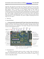
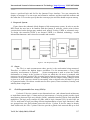
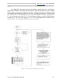
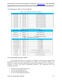
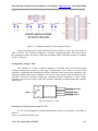
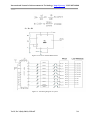
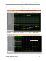
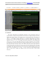
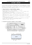
International Journal of Advancements in Technology http://ijict.org/ ISSN 0976-4860 FPGA Based Design & Implementation of Embedded System for Tilt Measurement S.M.Gulhane Mr. A.R.M.Khan Department of Electronics & Telecommunication, Jawaharlal Darda Institute of Engg.& Technology, Yavatmal Department of Electronics & Telecommunication, Jawaharlal Darda Institute of Engg.& Technology, Yavatmal S.L.Badjate Department of Electronics & Telecommunication, S.B.Jain Institute of Technology,Management and Research Nagpur Corresponding author: [email protected] Abstract Measurement of tilt is having a very much importance in the applications such as railway track monitoring, mining, aviation, tunneling, bridge and dam monitoring system, etc. The tilt is measured in terms of degrees and is made with respect to the original tilt of the surface on which the meter is kept. This paper proposes an embedded tilt measurement system, which uses a level sensor, A/D converter, Altera DE2 board and a controller designed in FPGA using VHDL with the help of QUARTUS II software. The proposed model of the tilt measurement system would measure the tilt based on an initial calibration and the Reference tilt set at the beginning. Here we have an output tilt which is available in degrees and it changes as per the input changes .The controller designed using VHDL would sense the changes in the inputs which is the change in the tilt, measured as 8 bit values (measured by level sensor and fed to DE2 board via A/D converter). Accordingly the tilt will be displayed using LCD module on Altera DE2 Board. The proposed system can be calibrated to get the specified precision in calculating the tilt. The system is able to calibrate the tilt up to required precision. The model will be scalable so that the input and output ranges could be easily changed as per the situation demands. Keywords: A/D converter, LCD module, VHDL, Cyclone-II EP2C35F72C6 FPGA, Altera Quartus II, ModelSim. 1. Introduction System is used to capture and calibrate the small changes in the level of the surface on which it is mounted, with respect to its initial position. The tilt or deflection of the system at its initial position is called as reference tilt and is always considered as „0‟ degree The designed system is a multipurpose embedded system for the measurement of tilt based on CYCLONE II FPGA. It has very much application in the field of aviation, robotics, dam monitoring system, bridge monitoring system, etc. This system mainly consists following parts ,level sensor, Simple A/D converter, Altera DE 2 Board Here a gravity based resistive sensor using a multi turn potentiometer pot is use to serve the purpose of capturing the inclination of surface. The output of a sensor is a voltage i.e. an analogue value which is dependent on the level or position of the surface on which it is mounted. If there is change or deflection in the level of surface the output of the sensor will vary depending on the amount of variation in the level of surface. Output of the level sensor is fed to the simple A/D converter which is used to convert the analogue value into corresponding 8 bit value i.e. the Vol 2, No 3 (July 2011) ©IJoAT 335 International Journal of Advancements in Technology http://ijict.org/ ISSN 0976-4860 digital data. This digital data corresponds to the amount of the changes in the level of surface which will be dependent on the o/p of the sensor (analogue value) fed to it. The O/P of the A/D converter is fed to the DE2 board via an expansion header slot provided on it through an IDE connector. There is provision of two expansion headers on DE2 board as GPIO(0)GPIO(1) Of which the expansion header GPIO(0)is used. The o/p of an A/D converter is given to the first eight I/O pins of the expansion header slot a controller designed in CYCLONE II FPGA chip provided on DE2 board with the help of VHDL and Quartus II, takes values available on expansion header slot and converts these values to the required format. The controller will display these values on the display provided on DE2 board in required format as e.g TILT:019.00 DEG. This system is capable of displaying the tilt in the range of 0 to 255 degrees. 2. Tools Used 2.1 Altera DE2 Board: Figure gives the block diagram of the DE2 board. To provide maximum flexibility for the user, all connections are made through the Cyclone II FPGA device. Thus, the user can configure the FPGA to implement any system design. It depicts the layout of the board and indicates the location of the connectors and key components. The DE2 board has many features that allow the user to implement a wide range of designed circuits, from simple circuits to various multimedia projects. Figure 1: Block Diagram of DE2 Board 2.2 Altera Quartus II The Quartus II development software provides a complete design environment for system-on-a-programmable-chip (SOPC) design. When working with the Quartus II software, you can specify options to customize your work environment. For example, you can Vol 2, No 3 (July 2011) ©IJoAT 336 International Journal of Advancements in Technology http://ijict.org/ ISSN 0976-4860 choose a preferred look and feel for the Quartus II user interface. You can customize the display of messages. You can create and customize toolbars, and show and hide toolbars and the status bar. You can also specify that the current project and files should reopen at startup, 3. Proposed System Figure shows the schematic block diagram of tilt measurement system. In order to use the DE2 board, the user has to be familiar with the Quartus II software, which exists in three versions based on the design entry method used, namely Verilog, VHDL or schematic entry. To design the controller VHDL is use because VHDL is a standard, technology / vendor independent language, and is therefore portable and reusable. Figure 2: The Proposed System 3.1 Sensor The Tilt is a static measurement where gravity is the acceleration being measured. Therefore, to achieve the highest degree resolution of a tilt measurement, a low-g, high sensitivity accelerometer is required. Sensor arrangement is used to sense the surface deformation or change in the position of object on which the tilt meter is mounted with respect to its reference position. We are using gravity based resistive sensor. When tilt occurs resistance of the potentiometer changes. According to this the output voltage changes which is given to A to D converter, which coverts analog value to digital value and then it is given to expansion header. We choose a multi-turn for more power, better resolution, linearity, and stability than a single turn. 3.2 Field-Programmable Gate Array (FPGA) Cyclone® II devices contain a two-dimensional row- and column-based architecture to implement custom logic. Column and row interconnects of varying speeds provide signal interconnects between logic array blocks (LABs), embedded memory blocks, and embedded multipliers. The logic array consists of LABs, with 16 logic elements (LEs) in each LAB. An LE is a small unit of logic providing efficient implementation of user logic functions. LABs are grouped into rows and columns across the device. Cyclone II devices range in density from 4,608 to 68,416 LEs. Cyclone II devices provide a global clock network and up to four Vol 2, No 3 (July 2011) ©IJoAT 337 International Journal of Advancements in Technology http://ijict.org/ ISSN 0976-4860 phase-locked loops (PLLs). The global clock network consists of up to 16global clock lines that drive throughout the entire device. The global clock network can provide clocks for all resources within the device, such as input/output elements (IOEs), LEs, embedded multipliers, and embedded memory blocks. The global clock lines can also be used for other high fan-out signals. Cyclone II PLLs provide general-purpose clocking with clock synthesis and phase shifting as well as external outputs for high-speed differential I/O support. M4K memory blocks are true dual-port memory blocks with 4K bits of memory plus parity (4,608 bits). These blocks provide dedicated true dual-port, simple dual-port, or single-port memory up to 36-bits wide at up to 260 MHz. These blocks are arranged in columns across the device in between certain LABs. Figure 3: FPGA Cyclone II EP2C35 Each Cyclone II device I/O pin is fed by an IOE located at the ends of LAB rows and columns around the periphery of the device. Each IOE contains a bidirectional I/O buffer and three registers for registering input, output, and output-enable signals. 3.3 LCD Module: The LCD module has built-in fonts and can be used to display text by sending appropriate commands to the display controller, which is called HD44780. A schematic diagram of the LCD module showing connections to the Cyclone II FPGA is given in Figure. Figure 4: Schematic diagram of the LCD module Vol 2, No 3 (July 2011) ©IJoAT 338 International Journal of Advancements in Technology http://ijict.org/ ISSN 0976-4860 The HD44780U dot-matrix liquid crystal display controller and driver LSI displays alphanumeric, Japanese kana characters and symbols. Since all the functions such as display RAM, character generator, and liquid crystal driver, required for driving a dot-matrix liquid crystal display are internally provided on one chip, a minimal system can be interfaced with this controller/driver. The HD44780U character generator ROM is extended to generate 208 (5 8) dot character fonts and 32 (5 10) dot character fonts for a total of 240 different character fonts. The low power supply (2.7V to 5.5V) of the HD44780U is suitable for any portable battery-driven product requiring low power dissipation. Figure 5: Flowchart demonstrating design of controller Vol 2, No 3 (July 2011) ©IJoAT 339 International Journal of Advancements in Technology http://ijict.org/ ISSN 0976-4860 4. Designing of Controller using VHDL Controller is designed in FPGA using VHDL. The programming flow can be well explained with flowcharts as given above in figure 5. 4.1 Internal Clock Utilization The DE2 board includes two oscillators that produce 27 MHz and 50 MHz clock signals. The board also includes an SMA connector which can be used to connect an external clock source to the board. The schematic of the clock circuitry is shown in figure 6. Figure 6 : Schematic diagram of the clock circuit 4.2 Generation of 400Hz clock In the design of the controller 50 Mz of crystal is utilize to generate the 400 Hz clock for the LCD display and the calculation are as follows 50MHz clock / 400Hz clock 1,25,000 (0F424 Hex )cycles 50MHz clock = = 1,25,000 Hence, 1 cycle of 400Hz Of clock Figure 7 : Generation of 400 MHz Clock Vol 2, No 3 (July 2011) ©IJoAT 340 International Journal of Advancements in Technology http://ijict.org/ ISSN 0976-4860 4.3 Creation of Design File The Compiler is a set of modules that transform design files in a project into output files for device programming and simulation. We can use the Compiler to run a full compilation, or we can run the individual modules separately. A full compilation processes a design with Analysis & Synthesis, the Fitter, and the Assembler, and the Classic or Time Quest Timing Analyzer, and allows you to optionally process the design with the Design Assistant, the EDA Netlist Writer, and the Compiler Database Interface. By default, the Compiler performs a timing-driven compilation. Figure 8 : Creation of Design File 4.4 Simulation in Quartus II The Quartus II Simulator is a tool for testing and debugging the logical operation and internal timing of our design. Because the Simulator allows us to verify our project before the project is actually committed to hardware, the Simulator can significantly shorten the time it takes to transform our initial design concept into working silicon. Depending on the type of information we need, we can perform a functional simulation to test the logical operation of our design, or we can perform a timing simulation to test both the logical operation and the worst-case timing for the design in the target device. We are using the Quartus II Simulator to simulate any design in a project. We can simulate a full design or any part of a design. 4.5 Node Finder The Node Finder is a search tool that allows us to find and use any node name in a compiled Quartus II project. We can search for specific node names or types of node names using custom or Altera-provided filters and other search criteria. We can limit the node name search to specific design entities, or you can search the entire project. Vol 2, No 3 (July 2011) ©IJoAT 341 International Journal of Advancements in Technology http://ijict.org/ ISSN 0976-4860 Figure 9 :Simulation in Quartus II 5. Synthesis of VHDL code 5.1 Pin Assignments: Assignments are used to control a variety of different functions of the Quartus II software and are an important part of an efficient and effective design. When used in conjunction with a solid design foundation, assignments can help us successfully compile our design. Assignments are logic functions we assign to a physical resource on the device, or compilation resources we assign to logic functions. Making assignments allows us to specify various options and settings for the logic in the design, including location, I/O standard, timing, logic option, parameter, simulation, and pin assignments. Figure 10: Pin Assignments in Quartus II Vol 2, No 3 (July 2011) ©IJoAT 342 International Journal of Advancements in Technology http://ijict.org/ ISSN 0976-4860 5.2 Utilized pins of FPGA Cyclone II EP2C35 Table 1: Pin utilized for Expansion Header Table2: Pin utilized for the clock input Table 3: Pin utilized for LCD 5.3 Loading VHDL Program in FPGA The Programmer allows us to program or configure all Altera devices supported by the Quartus II software with files generated by the Compiler. The Assembler module of the Quartus II Compiler generates programming files that the Programmer can use to program or configure a device with Altera programming hardware. The Programmer has four programming modes: In Passive Serial programming mode, In JTAG programming mode, In In-Socket programming mode, In Active Serial programming mode, Vol 2, No 3 (July 2011) ©IJoAT 343 International Journal of Advancements in Technology http://ijict.org/ ISSN 0976-4860 To demonstrate the designed we have used ASP mode. Figure 11 : Active Serial programming mode 6. Design Of Hardware 6.1 Analogue to Digital Converter: The system uses simple 0809.It converts analogue o/p of level sensor to 8 bit digital value. This digital value is fed to the DE2 board through expansion header slot.The decimal equivalent digital output value D for a given analogue input voltage Vin can be calculated from the relationship. D = (Vin / Vref)*256 Figure 12: ADC 0808/0809 6.2 Expansion Header The DE2 Board provides two 40-pin expansion headers GPIO 0, GPIO 1. Each header connects directly to 36 pins on the Cyclone II FPGA, and also provides DC +5V (VCC5), DC +3.3V (VCC33), and two GND pins are brought out to two 40-pin expansion connectors 40pin header is designed to accept a standard 40-pin ribbon cable used for IDE hard drives. Each pin on the expansion headers is connected to two diodes and a resistor that provide protection from high and low voltages. Vol 2, No 3 (July 2011) ©IJoAT 344 International Journal of Advancements in Technology http://ijict.org/ ISSN 0976-4860 Figure 13 : Schematic diagram of the expansion header In the tilt measurement system proposed here uses GPIO 0 to give the 8 bit output of ADC to FPGA. The connection diagram is as shown in following figure. The figure shows the protection circuitry for only 8 of the pins on header GPIO 0, but this circuitry is included for all 72 data pins. 6.3 Regulator using IC 7805 The LM7805 IC of three terminal regulators is available with several fixed output voltages making them useful in a wide range of applications. One of these is local on card regulation, eliminating the distribution problems associated with single point regulation. The voltages available allow these regulators to be used in logic systems, instrumentation, Hi-Fi, and other solid state electronic equipment. Although designed primarily as fixed voltage regulators, these devices can be used with external components to obtain adjustable voltages and currents. Figure 14: Regulator IC 7805 6.4 Design of clock generator using IC 555 IC 555 can be designed as Astable Multivibrator to give o/p frequency of 25 KHz as follows: Since, we require 50% duty cycle. Vol 2, No 3 (July 2011) ©IJoAT 345 International Journal of Advancements in Technology http://ijict.org/ ISSN 0976-4860 So, Ra= Rb Figure 15: IC 555 as Astable Multivibrator Figure 16 : Interfacing diagram of system Vol 2, No 3 (July 2011) ©IJoAT 346 International Journal of Advancements in Technology http://ijict.org/ ISSN 0976-4860 7. Simulation Results using MODELSIM For design of controller we have used modelsim for simulation. Test value 1 : VALUE: 00000111, S_UNITS: 30 , S_TENS: 30 , S_THOUSANDS: 37 Test value 2 : VALUE: 00100101 , S_UNITS: 30 , S_TENS: 33, S_THOUSANDS: 37 Vol 2, No 3 (July 2011) ©IJoAT 347 International Journal of Advancements in Technology http://ijict.org/ ISSN 0976-4860 Test value 3 : VALUE: 01110001, S_UNITS: 31, S_TENS: 31, S_THOUSANDS: 33 8. Conclusions This paper demonstrate the Embedded controller for tilt measurement where an external sensor is used for tilt measurement .The sensor has 5 outputs and gives the tilt in digital angle format .Being a 5 bit output device, it can measure tilt to an accuracy of 360/2^5 = 11.25 degrees, each bit indicates a 11.25 degrees approximate tilt, from the reference tilt. To further elucidate the point let us take an example, the output 00110 indicates a tilt of 6 * 11.25 = 67.25 degree tilt from the reference tilt. This measured tilt will be given to the Altera DE2 Board and the tilt would be displayed on the LCD.The LCD data pins as present on the board are used. the expansion slot 1 is used as the slot to take input from the tilt meter sensor. The VHDL code that will be burnt inside the Cyclone chip would convert this value into a proper tilt value and then produce the output accordingly. The output produced out of this conversion would be shown on the LCD screen. The LCD operates on a 27 states , 11 state are used for initialization and the other 16 states write a single line output on the LCD in the form of ASCII HEX characters . Vol 2, No 3 (July 2011) ©IJoAT 348 International Journal of Advancements in Technology http://ijict.org/ ISSN 0976-4860 References [1] J.Bhasker “VHDL PRIMER”, Third Edition, Pearson Education Pte. Ltd. Pub. Co., 2003. [2] Douglas L. Perry “VHDL Programming by Examples”, Fourth Edition, Tata Mc Graw-Hill, 2002. [3] Kenneth Ayala “The 8051 microcontroller Architecture & programming & Applications" Second Edition, Penram [4] Kamal “Embedded Systems: Architecture, Programming and Design” Publisher: Mcgraw-Hill Science/engineering/math. [5] “FPGA-based Implementation of Digital Logic Design using Altera DE2 Board” Zeyad Assi Obaid, Nasri Sulaiman and M. N. Hamidon IJCSNS International Journal of Computer Science and Network Security, VOL.9 No.8, July 2009 [6] “Implementing an I2C Master Bus Controller in a FPGA for Maxim DS3232”, April 2008 Enoch Hwang. [7] Altera “DE2 Development and Education Board” DE2 Package, or [available online at] http://www.altera.com [8] Altera “DE2 Development and Education Board, user manual” Version 1.42,2006, http://www.altera.com. Vol 2, No 3 (July 2011) ©IJoAT 349