1
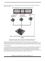
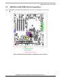
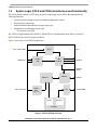
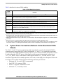
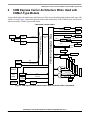
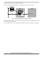
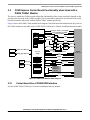
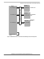
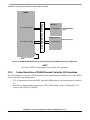
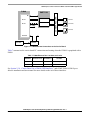
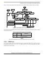
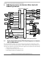
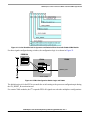
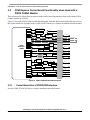
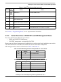
Freescale Semiconductor
Design Workbook
Document Number: COMEXPRSDS
Rev. 1, 02/2011
COM Express Carrier Development System
Design Workbook
This document primarily describes the COM Express carrier
board, its relationship to the whole COM Express
development system, and the differences between the carrier
board’s architected functions depending on the processor
module in use.
The COM Express carrier development system, referred to
in this document as COMExprsDS, is a high-performance,
computing, evaluation, and development platform
supporting a single-board computing (SBC) COM Express
module based on Power Architecture® processor.
The COM Express carrier board is a lead-free,
RoHS-compliant board that supports various COMe
processor module types. Each COMe processor module
(hereafter referred to as COMe module) includes a primary
processor or one of its derivatives, and Figure 1 shows how
the various modules plug into the common carrier board.
© 2011 Freescale Semiconductor, Inc. All rights reserved.
Contents
1. COMExprsDS Features and Architecture . . . . . . . . . . 3
1.2. Difficult-to-Find COMe Carrier Connections . . . . 7
1.1. COMExprsDS as a Processor Evaluation System . 5
2. COM Express Carrier Architecture When Used with
COMe1-Type Module . . . . . . . . . . . . . . . . . . . . . . . . 11
3. COM Express Carrier Architecture When Used with
COMe2-Type Module . . . . . . . . . . . . . . . . . . . . . . . . 30
4. Programming Model . . . . . . . . . . . . . . . . . . . . . . . . . 48
5. Revision History . . . . . . . . . . . . . . . . . . . . . . . . . . . . 49
A. References . . . . . . . . . . . . . . . . . . . . . . . . . . . . . . . . 49
Table 1 shows the processors currently supported by each COMe module type and the orderable part
number for each kit.
Table 1. Supported Processors and Kit Ordering Information
COMe Module Type
Processor
Kit Part Number
COMe1
P4080
P4080COMe-DS-PB
COMe2
P2020
P2020COMe-DS-PB
Figure 1. How Various Module Types Fit into the Common Carrier Board
NOTE
In the future, the COM Express carrier board will support the P5020/P5010,
P4040, P3041, P2010, P1021, P1020, P1011, P1012, and P1013 devices.
Having a common carrier architecture that supports all of these devices as plug-in modules saves
development time and money, because many devices can be evaluated with only a single investment in the
remaining components of the development system; the peripheral IO modules, chassis, and power supply
remain unchanged.
The COMExprsDS feature set is determined primarily by the type of COMe module in use and then by the
actual processor on the module. Based on this feature set, the development system provides typical
OS-dependent resources (disk, Ethernet, and so on) for that configuration. Therefore, this document
describes the general development system features first, followed by the COMe module type features, and
then the processor device specifics and how they are used by the carrier board.
COM Express Carrier Development System Design Workbook, Rev. 1
2
Freescale Semiconductor
COMExprsDS Features and Architecture
1
COMExprsDS Features and Architecture
The general features of the COMExprsDS are as follows:
• Carrier/COMe connectors and supported functions that include the following:
— Standard ATX power supply connector
— One SD card/MMC connector
— Two dual CAN connectors
— SerDes PCI-Express (PCIe) connector
– Five PCIe x4 connectors (connector “A” through connector “F”), which can support up to
four lanes of PCIe 2.0/1.0, SGMII, sRIO, and XAUI, depending on what processor is used
– Two PCIe x1 connectors (used as sideband connectors for the PCIe x4 connectors) and one
PCIe x1 connector used for a TDM riser to support SLIC functionality
— Eight USB2.0 connectors
— Four SATA II connectors
— One DVI-I connector to support either analog VGA (via an adapter) or digital DVI connector
— LVDS A and B ports to support two, single-link DFP (TFT panel) displays with optional LVDS
panel and touchscreen functionality
— Two UART DB-9 RS-232 connectors (UART0/1 serial ports) that operate at up to 115200 Kbps
— One stereo audio jack
— Three gigabit Ethernet ports 0/1/3 supporting one dual and one single GMII (1-GHz) RJ-45
Ethernet connectors
– One dual-port PHY supporting one dual RMII (100/10-MHz) connector for COMe2 (only
for processors that feature QUICC Engine (QE) functionality).
— IXXAT
– 50-pin connector for Industrial Ethernet Module via SPI bus
— Tamper detect circuitry to test out P5020/P3040 security modes
— SLIC
– RJ-11 phone connectors can be added by using a TDM riser card into slot 5 and the TDM
riser sideband connector
— RS-485 can be added by adding an adapter to the DB-9 RS-232 connector.
• Multifunction FPGA
— Routes low-speed and user-defined signals from the COMe module board connectors to the
appropriate connectors and devices located on the COM Express carrier board.
— Programmed by the processor on the COMe module following a power-up or hard reset. The
FPGA functionality varies depending on the specific processor populated on the COMe
module.
— Generally interfaces to the following signal groups on the COMe module connectors:
– Reserved/user-defined
– UART2 and UART3
COM Express Carrier Development System Design Workbook, Rev. 1
Freescale Semiconductor
3
COMExprsDS Features and Architecture
•
•
– TDM
– SSI
– GPI
– GPO
— Interfaces to the following connectors and devices on the COM Express carrier board for
processors that feature QUICC Engine (QE) functionality:
– Τwo RS-232 serial ports with corresponding DB9 connectors (UART 2/3)
– Two RS-485 serial ports with corresponding DB9 connectors
– Four CAN ports with corresponding connectors
– UTOPIA module and connector using Freescale PQ-MDS-QOC3 card
– HDLC module and connector using Freescale PQ-MDS-16T1E1 card
– TDM-based SLIC modules
– Fast Ethernet PHY (RMII/MII)
– SSI-based CODECs
– 1588 header—support is TBD
Other functions routed from the COMe module to carrier board devices are:
— Local bus
– 128-Mbyte NOR FLASH on COMe1 module for Freescale debug purposes only
— eSDHC
– Connects to SDMedia card slot for boot code or mass storage
— SPI
– 16-Mbyte EEPROM module for boot code and storage
– Control interface for LVDS touchscreen
— I2C
– Three I2C controllers from COMe module
– One I2C2 master implemented in FPGA to read I2C2 EEPROM to determine processor type
– I2C1 to I2C expander to generate eight GPIOs (five to FPGA, three to IXXAT module)
– I2C2 to control LVDS interface and FPGA I2C2 slave mux/demux for COMe2
(P1021/P1012 only)
– I2C3 to control DVI/VGA interface and FPGA I2C3 slave mux/demux for COMe2
(P1021/P1012 only)
— Debug features
– Legacy COP/JTAG and USBTAP headers for use with CodeWarrior software
System logic CPLD and FPGA—other functions
— CPLD manages power sequencing
— Enabling/disabling of functions based on processor type
— Mux/demux functions for QE functions, based on I2C2 or I2C3 slave register settings
— I2C1 master reads processor type
COM Express Carrier Development System Design Workbook, Rev. 1
4
Freescale Semiconductor
COMExprsDS Features and Architecture
•
•
Clocks
— SerDes clock
– Two clock buffers
– Sd_refclk1 pair supports PCIe, and sd_refclk2_p/n supports SGMII and XAUI
Power supplies
— Power is supplied to carrier board via standard ATX power supply
— Power is supplied to COMe module via +12 V pins, VCC_RTC=3.3 V, and VCC_5V_stby =
5 V on the COM Express connectors
— 2.5-V power for RMII Ethernet PHY
1.1
COMExprsDS as a Processor Evaluation System
For general hardware and/or software development and evaluation purposes, the COMExpress
development system can be used like an ordinary, desktop computer.
The P4080COMe-DS-PB and P2020COMe-DS-PB development systems can also be used to evaluate
many features of the P4080 and P2020 processors, respectively. Table 2 summarizes the processor
hardware interfaces that can be evaluated by using the COM Express carrier board; note that shaded
features apply to only one processor.
Table 2. COMExprsDS Device Interfaces
Device Feature
SerDes
LVDS
eSDHC
SPI
Local bus
Serial
I2C
Configuration Options
• Connect to PCI Express slots for use with graphics or other PEX cards
• Test via PCI Express card (typically graphics) or Catalyst™ PCI Express control/monitoring card
Use ports A or B to test single-link DFP using LVDS TFT LCD panel and touch screen for applicable modules
For P2020 only: Supports SDMedia cards and MMC cards
Supports standard and x4 devices
For P4080 only: Internal debug
UART supports two 4-wire serial ports
I2C bus #1 can be used for the following:
• Boot initialization code
• System EEPROM (MAC address storage, serial number, and so on)
• Processor EEPROM for COMe module and processor ID from I2C master in the carrier FPGA
• Expander to interface to I2C slave in the carrier FPGA (TBD)
I2C bus #2 can be used for the following:
• RTC on the COMe module
• interface to LVDS control
I2C bus #3 can be used for the following:
• interface to VGA control
Clocking
GPIO
• SerDes clock buffers for XAUI/SGMII/Serial RapidIO and PCI Express slots
• RMII clock and buffers
Eight GPIOs come from I2C expander
COM Express Carrier Development System Design Workbook, Rev. 1
Freescale Semiconductor
5
COMExprsDS Features and Architecture
Table 2. COMExprsDS Device Interfaces (continued)
Device Feature
Configuration Options
IRQs
EVENT switch normally asserts IRQ* but can drive SRESET0, and/or SRESET1 via software setting
Power
ATX power supply to COMExpress connector VCC_12, VCC_5_STBY, VCC_RTC_BAT
1.1.1
Development System Use
In the absence of special hardware or software configuration, the COMExpress development system
operates identically to a development/evaluation system such as ArgoNavis (8641DS) or other members
of the HPC family.
1.1.2
Embedded Use
Section 2.2, “Carrier Board Configuration Switches When Used with a P4080 COMe1 Module,” and
Section 3.2, “Carrier Board Configuration Switches in a System with a P2020 COMe2 Module,” provides
the FPGA and external configuration switch settings used for start up configuration information for
U-Boot or Linux when the system is used as an embedded platform.
COM Express Carrier Development System Design Workbook, Rev. 1
6
Freescale Semiconductor
COMExprsDS Features and Architecture
1.2
Difficult-to-Find COMe Carrier Connections
Figure 2 highlights connections that are difficult to find on the COM Express carrier board.
Key:
ATX power connector
SW3 power-on button
SW1 local reset
CPLD programming header
FPGA programming header
Figure 2. Difficult-to-Find Connections—COM Express Carrier Top View
COM Express Carrier Development System Design Workbook, Rev. 1
Freescale Semiconductor
7
COMExprsDS Features and Architecture
1.3
System Logic (CPLD and FPGA) Architecture and Functionality
The carrier board contains a CPLD used for power sequencing, and an FPGA that implements the
following functions:
• Transfers switch settings to processor/board configuration signals
• Performs reset sequencing
• Enables/disables functions based on processor type
• Implements miscellaneous system logic:
— I2C timeout reset-TBD
The CPLD is implemented with a MAX II, and the FPGA is implemented in an Altera Cyclone III
EP3C16F484C8 in a 484-256-pad micro-BGA.
Figure 3 shows the overall FPGA architecture.
PSU_PWR_GOOD
RESET SW
CPU
CPLD
REG
RESET
SEQ
RESETS
RESETS
CONFIG
DRIVE
CONFIG
REGFILE
8-BIT LAD LBUS
LOCAL
BUS
I2C1
CONFIG
I2C EEPROM
(debug only)
SLAVE
MASTER
I2CLOGIC
Figure 3. CPLD and FPGA Overview
COM Express Carrier Development System Design Workbook, Rev. 1
8
Freescale Semiconductor
COMExprsDS Features and Architecture
Table 3 describes the various FPGA modules.
Table 3. FPGA Module Descriptions
FPGA
Modules
RESETSEQ
Function
Collects various reset/power-good signals and starts the global reset sequencer1, 2
REGRESETS Copies reset signals from the sequencer, but also allows register-based software to individually asserted reset
to the local bus, memory, and/or compact FLASH interfaces.
REGFILE
LOCALBUS
CONFIG
1
2
3
4
5
A multi-ported register file containing status and configuration data3
Interface between the processor and REGFILE for internal Freescale debug use only4
Monitors and/or sets selected configuration signals5
I2CLOGIC
and I2C1
The I2C1 master reads COMe module EEPROM at address 0xA8 to detect processor type and id information.
An I2C slave is also used to select muxes for QE functions via the I2C1 expander FPGA_IO signals (first
availability is for P1021 COMe2 module).
Power
Power for FPGA is supplied from dedicated VCC_HOT_3.3 and VCC_HOT_1.5-V power supplies based upon
the ATX power supply +5-V standby power, VCC5STDBY.
ASLEEP indicates that the processors(s) have exited the reset state. It does not cause a reset, because the processor can
sleep for any number of reasons after hard reset is completed.
During power-down, all I/O and output drivers are tristated. After power up, drivers may be driven. Normal operation and/or use
of the VELA engine may cause some I/Os to be tristated.
REGFILE must be able to accept (or arbitrate for) concurrent writes to the same register, though this is not a statistically likely
occurrence.
Because access to the internal registers may be blocked, asynchronous (not ready) signalling is used.
In some instances, CONFIG maps switch settings into direct configuration outputs, while in others (such as SYSCLK), it maps
a 3-position switch into a 16-bit register initialization pattern, which is subsequently used to initialize the clock generator.
1.4
System Power Connections Between Carrier Board and COMe
Module
The 12-V, 5-V, and 3.3-V power requirements of the carrier board are met by the attached ATX-12V
compatible power supply unit (PSU) of the COMExprsDS. 5 V and 3.3 V are connected to individual
power planes in the COMExprsDS PCB stackup. The 12-V power from the standard ATX header is treated
as separate from the ATX-12V power, which supplies a large amount of current and is referred to as
“VCC_12V_BULK” to the COMe module. Other supplies include VCC_5VSTBY, and VCC_BAT.
Note that to support the FPGA standby operation, video cards, or other high-power-dissipation cards in the
PCI Express slot, the PSU should support the following minimum specifications:
• Minimum 450 W overall, 500 W recommended
• One PCIE 12-V connector (TBD)
• PCIE 12 V supports a minimum of 150 W
• Minimum 5-V, 2-A standby current
COM Express Carrier Development System Design Workbook, Rev. 1
Freescale Semiconductor
9
COMExprsDS Features and Architecture
All other power sources are also derived from the ATX PSU. Figure 4 shows the principal system power
connections in relationship to the CPLD control. For more detail about the processor power scheme
implemented by this system, see “Power” in Table 3.
ATX PSU
PWRON
PWRGD
+3.3VHOT
+5VSTB
SPS
Raptor
+1.8VHOT
LDO
+5 V
LDO
+2.5 V
LDO
+1.8 V
LDO
+1.2 V
Select
VSTANDBY
+3.3 V
+12 V
+3.3 V HOT
+12V_BULK
Batt.
Figure 4. COMExprsDS System Power Supplies
COM Express Carrier Development System Design Workbook, Rev. 1
10
Freescale Semiconductor
COM Express Carrier Architecture When Used with COMe1-Type Module
2
COM Express Carrier Architecture When Used with
COMe1-Type Module
As described earlier, the architecture and feature set of the carrier board depends on the module type with
which it is used. Figure 5 depicts the general features and connectivity of the COM Express carrier board
when used with a COMe1-type module board.
COMEXPRESS CARRIER (COMe1)
3 x RJ-45
MIDI
GBE0-3
4 USB 2.0 ports
4 DUAL USE
HDRS
4 USB 2.0 ports
Only UART3
RS-485
Adapter
NOR
Flash
LBC
QE/UART/
User-defined
GPIO
SPIFlash
DVI/VGA
LVDS
TouchIF
SPI
SPIFlash
SDHC
SD/MMC conn
SB
Lanes 16-19
2Singlelink
DFP CONN
Lanes 20-23
DVI
Lanes 24
Lynx2
PCIe slot5
Lanes 4-7
PCIe slot4
Lynx1
PCIe slot3
PCIe slot2
Lanes 0-3
DVI-I
FPGA
IXXAT (IEM) CONN
I2C#3
I2C#2
VGA
CLOCKS
ATX
CONN
5 GPIOs
3 GPIOs
I2C
Expander
SB
1588 SIGNALS
1588
HDR
I2C#1
Tamper det
hdr
STM1403A
SECURITY
PCIe slot1
CAN
4CAN
CONN
FSL COMe Connector
UART2/3
RS232
FPGA and External Muxes
Dual DB9
sata3
LVDS A/B
SATA x1
sata2
sata1
sata0
FAN HDR
Dual
DEM9
RS232
UART0/1
Figure 5. COM Express Carrier Block Diagram When Used with COMe 1-Type Module
COM Express Carrier Development System Design Workbook, Rev. 1
Freescale Semiconductor
11
COM Express Carrier Architecture When Used with COMe1-Type Module
2.1
System Reset Performed by FPGA Reset Sequencer in a System
with a COMe1 Module
The carrier board FPGA contains a reset sequencer that properly manages the orderly bring-up of the
system (this is not the same as the power sequencer, which is similar, but not specifically related to reset).
After the system transitions to having fully stable power supplies, the reset sequencer does the following:
1. Waits for all reset conditions to clear
2. Configures and releases the processor from reset
3. Idles waiting for further reset conditions to occur
Table 4 summarizes the reset conditions and actions of the FPGA when used with a COMe1 module.
Table 4. Reset Conditions and Actions of FPGA Reset Sequencer
Signal
Type
Description
Action
HOT_RST_B
External HOT power stable
Restarts all FPGA internal state machines and registers
PWRGD
External ATX power stable
Causes full system reset unless the system is in S3 (power
down) state
SYS_HRST_B
External COP tool reset request
Upon power good, sys_rst_b is sent from carrier to COMe1
module
RESET_REQ_B External CPU requests reset
2.2
Full reset
Carrier Board Configuration Switches When Used with a P4080
COMe1 Module
There are different types of carrier board configurations. A list of these configuration types and their
implementation is shown in Table 5.
Table 5. Carrier Board Configuration Types
Configuration Type
Implementation
Requires software configuration to Implemented with “DIP switches” and/or software-settable options
support evaluation
Expected to be easily or often
changed by the end-user or
developer
COM Express Carrier Development System Design Workbook, Rev. 1
12
Freescale Semiconductor
COM Express Carrier Architecture When Used with COMe1-Type Module
The carrier board switches and their default settings when used with a P4080 COMe module are shown in
Figure 6. Switch names exactly match the name on the schematics and on the printed-circuit board in most
cases, except where a spare has been newly assigned and only the FPGA has changed.
Figure 6. Carrier Board Switch Assignments and Defaults When Used with P4080 COMe Module
COM Express Carrier Development System Design Workbook, Rev. 1
Freescale Semiconductor
13
COM Express Carrier Architecture When Used with COMe1-Type Module
For those signals configured using switches, the configuration logic is as shown in Figure 7.
EEPROM
OVDD
SW1
EN1
SW2
EN2
...
P4080
FPGA
CFGDRV
ENx.y
SWx.y
CONFIG_PIN
where needed
Figure 7. COMe1 Configuration Switch Logic and P4080
The default action is for the FPGA to transfer the switch setting to the processor configuration pin during
the CB_RESET_B assertion interval.
For certain COMe modules, the I2C expander FPGA IO signals can select the multiplexer configurations.
COM Express Carrier Development System Design Workbook, Rev. 1
14
Freescale Semiconductor
COM Express Carrier Architecture When Used with COMe1-Type Module
2.3
COM Express Carrier Board Functionality when Used with a
P4080 COMe1 Module
The ways in which the COMe1 module affects the functionality of the carrier board also depends on the
specific processor used in the COMe1 module. This section and its subsections are tailored to the carrier
board functionality when used with the P4080 COMe1 module specifically.
Figure 8 shows the P4080 COMe module block diagram. Note that functional modules that only exist on
the COMe module are described in the COMX-P4080 COM Express Module installation and user manual.
x4 PCIe
4x1G-SGMII 4x1G-SGMII
10G-XAUI
10G-XAUI
x4SERDES x4SERDES
either here or there
4x1G-SGMII
x4 PCIe
x4 PCIe
x4SRIO
x4SRIO
8xSERDES
Aurora
Debug
2xSERDES
SO-DIMM
DDR3 1333/1600 72-bit
SO-DIMM
DDR3 1333/1600 72-bit
Freescale
P4080
5020/4080
10G-XAUI / x4PCIe / 4x1G-SGMII
x4PCIe/4xSRIO/4x1G SGMII
x4PCIe/4xSRIO
1G-T
RGMII
1G-T
PHY
RGMII/USB
1G-T
PHY
1G-T
5020/3041
5xUSB
USB
4xUSB2.0
USB2.0
Hub
PHY
5xUSB
USB
USB ULPI
4xUSB2.0
USB2.0
Hub
PHY
5020/3041
USB PHY 5020/3041
5020/3041
USB PHY
COM-E
2xUART(Tx/Rx/CTS/RTS)
Connectors
SPI
SDIO/MMC
2xSATA
4xI2C
5020
SPI (3 CS#)
Debug
Header
JTAG/COP
SD/MMC
Debug
Header
x1 Aurora
2x USB2.0 ULPI
4xI2C
RTC_CLK
2xRGMII
2xUART
(Tx/Rx/CTS/RTS)
Or 4xUART (Tx/rX)
Local Bus
2xIEEE-1588
LocalBus
RTC/
WDT
RTC_BAT
WDT
8xGPIO
NOR Flash
Uboot FW
NAND Flash
OS/App
1588 (Trig/Alarm/Clock/Pulse/Stamp-Tx/Rx)
Reset
Tamper Detect
Figure 8. P4080 COMe Module Block Diagram
2.3.1
Carrier Board Use of P4080 DDR Interface
See the COMX-P4080 COM Express Module installation and user manual.
COM Express Carrier Development System Design Workbook, Rev. 1
Freescale Semiconductor
15
COM Express Carrier Architecture When Used with COMe1-Type Module
2.3.2
Carrier Board Use of P4080 SerDes x18 Interface
The SerDes block on the P4080 provides high-speed serial communications interfaces for several internal
devices. The SerDes block on the P4080 COMe1 module provides 18 serial lanes for the carrier that may
be partitioned as shown in Table 6.
Note that the term ‘lane’ is used to describe the minimum number of signals needed to create a
bidirectional communications channel; in the case of PCI-Express or Serial RapidIO, a lane consists of two
differential pairs, one for receive and one for transmit, or four in all.
Table 6, top down, shows the following clocking banks and how they are configured by the carrier board:
• Bank1—lanes A–D go to slot 1, E–H to slot 2, and I–J to the Aurora debug connector
• Bank2—lanes A–D go to slot 3
• Bank3—lanes A–B go to SATA ports 1 and 2
Table 6. P4080 SerDes Lane Multiplexing Configurations on Carrier
Bank 1
Bank 2
Bank 3
A
B
C
D
E
F
G
H
I
J
A
B
C
D
A
B
C
D
0
1
2
3
4
5
6
7
8
9
10
11
12
13
14
15
16
17
SATA
Port1
SATA
Port2
—
—
Aurora Conn on
COMe Module
SLOT 3
PCIe2
(5/2.5G)
Debug (5/2.5G)
XAUI FM2
SATA1 SATA2
—
—
PCIe1
(5/2.5G)
SGMII SGMII SGMII SGMII
FM2
FM2
FM2
FM2
Debug (5/2.5G)
XAUI FM2
SATA1 SATA2
—
—
sRIO2
(2.5G)
sRIO1
(2.5G)
Debug (5/2.5G)
XAUI FM2
SATA1 SATA2
—
—
sRIO2
(2.5G)
sRIO1
(2.5G)
Debug (2.5G)
SGMII SGMII SGMII SGMII SATA1 SATA2
FM2
FM2
FM2
FM2
—
—
sRIO2
(2.5G)
sRIO1
(2.5G)
Debug (5/2.5G)
PCIe3
(5/2.5G)
SATA1 SATA2
—
—
PCIe1
(5/2.5G)
sRIO1
(2.5G)
Debug (5/2.5G)
XAUI FM2
SATA1 SATA2
—
—
SLOT 1
SLOT 2
PCIe1
(5/2.5G)
COM Express Carrier Development System Design Workbook, Rev. 1
16
Freescale Semiconductor
COM Express Carrier Architecture When Used with COMe1-Type Module
PEX Slot 1
P4080
SD_TX/RX[0:3](p,n)
SD_TX/RX[8:9](p,n)
COMEXPRS CONN
SD_TX/RX[4:7](p,n)
TX/RX[0:3](p,n)
PCIe/SRIO Cards
PEX Slot 2
TX/RX[4:7](p,n)
Aurora Conn
PCIe/SGMII/SRIO
Cards
Aurora Debug
Connector
TX/RX[1:0](p,n)
REFCLK_SD1(p,n)
100 MHz
Figure 9. P4080 SerDes Bank1 to Carrier Board Cards/Debug Connector Configuration
COM Express Carrier Development System Design Workbook, Rev. 1
Freescale Semiconductor
17
COM Express Carrier Architecture When Used with COMe1-Type Module
SD_TX/RX[10:13](p,n)
SD_TX/RX[14:15](p,n)
COMEXPRS CONN
P4080
PEX Slot 3
TX/RX[0:3](p,n)
PCIe/SGMII/XAUI
Cards
SATA port1 & 2
SATA connectors
TX/RX[1:2](p,n)
REFCLK_SD2/3(p,n)
125 MHz
Figure 10. P4080 SerDes Bank 2 and 3 to Carrier Board Cards/SATA Connector Configuration
NOTE
The SD2 and SD3 clocking domains use separate clock generators.
2.3.3
Carrier Board Use of P4080 Ethernet Controller (EC) Interfaces
The carrier board uses up to two 10/100/1000baseT triple-speed Ethernet controllers (ECs) of the P4080
in one of the following configurations:
• EC2 is connected to the on-board PHY using the RGMII protocol; the remaining ports are unused.
or
• Both ECs are independently connected to a ULPI USB interface; for the COMExprsDS, EC2
routes via the ULPI to a USB PHY.
COM Express Carrier Development System Design Workbook, Rev. 1
18
Freescale Semiconductor
COM Express Carrier Architecture When Used with COMe1-Type Module
P4080
ENET PHY
EC #1
1
EC #2
2
COMEXPRS CONN
MI
To USB2
Port #1
Port #2s
Port #3
GTXCLK
CLKBUF
125 MHz
Figure 11. P4080 Ethernet Connections to the Carrier Board
Table 7 summarizes the carrier board EC connections and routing when the COMe1 is populated with a
P4080.
Table 7. P4080 Ethernet Port Locations on Carrier
P4080 EC # Connection Port PHY Address
Location
1
1
0
Conn. P9 top
2
2
1
Conn. P9 bottom
See Section 2.3.8, “Carrier Board Use of P4080 USB Interfaces,” and COMX-P4080 COM Express
Module installation and user manual for more details on the use of these interfaces.
COM Express Carrier Development System Design Workbook, Rev. 1
Freescale Semiconductor
19
COM Express Carrier Architecture When Used with COMe1-Type Module
2.3.4
Carrier Board Use of P4080 Support for IEEE Std 1588™Protocol
The carrier board supports the P4080 IEEE 1588 precision time protocol (PTP) as shown in Figure 12. This
facility works in tandem with an Ethernet controller to time-stamp incoming packets.
P4080
TX >
1588
ALARMOUT[1:2]
TRIGIN[1:2]
STMP_TX/RX[1:2]
XTALOSC
125.000 MHz
±25 ppm
CLKIN
CLKOUT
P6880
Debug Header
PULSEOUT[1:2]
Figure 12. P4080 IEEE 1588 Interface to Carrier Board P6880 Debug Header
2.3.5
Carrier Board Use of P4080 Local Bus Interface
See the COMX-P4080 COM Express Module installation and user manual for details. Local bus
connection to the carrier board is for Freescale internal use only.
COM Express Carrier Development System Design Workbook, Rev. 1
20
Freescale Semiconductor
COM Express Carrier Architecture When Used with COMe1-Type Module
2.3.6
Carrier Board Use of P4080 eSDHC Interface
The P4080 has an enhanced secure digital host controller (eSDHC). The carrier board connects the P4080
eSDHC to an SDMedia card slot and uses GPIO signals for sideband signals, such as write-protect-detect
and card-detect. Both x4 and x8 cards are supported, the latter using the SPI_CS_B[0:3] signals, which
can be reassigned as eSHDC_D[4:7].
P4080
SDMedia Slot
SDHC_CMD
SDHC_CLK
SDHC_CD
SDHC_WP
SDHC_DAT[4:7]
COMEXPRS CONN
SDHC_DAT[0:3]
CMD
DAT[0:3]
CLK
SDHC_CD_B
SDHC_WP_B
CD_B
WP_B
DAT[4:7]
SD
CFG_SDX8MUX
Figure 13. P4080 eSDHC Interface to Carrier Board SD Media Card Slot
NOTE
SDHC_DAT[4:7] are shared with the SPI CS pins; the CFG_SDX8MUX
switch selects the routing of those pins to either the SDHC devices or the
SPI devices, but both cannot be used simultaneously.
COM Express Carrier Development System Design Workbook, Rev. 1
Freescale Semiconductor
21
COM Express Carrier Architecture When Used with COMe1-Type Module
2.3.7
Carrier Board Use of P4080 SPI Interface
The P4080 has a serial peripheral interface (SPI), which is used to communicate with various peripherals.
The COM Express carrier board connects a conventional 16-Mbyte serial SPI FLASH EEPROM to one
chip-select of the P4080 SPI interface. The remaining three chip-selects are unused.
P4080
SPI_MOSI
SPI_MISO
SPI_CS0_B
COMEXPRS CONN
SPI_CLK
SPI FLASH
16 Mbytes
SPI_CS1_B
SPI_CS3_B
MUXES
SPI_CS2_B
cfg_SDX8MUX
sw_FLASHWP_B
Figure 14. P4080 SPI Interface Connection to Carrier SPI FLASH Slot
COM Express Carrier Development System Design Workbook, Rev. 1
22
Freescale Semiconductor
COM Express Carrier Architecture When Used with COMe1-Type Module
2.3.8
Carrier Board Use of P4080 USB Interfaces
The P4080 has a USB 2.0 port that uses the UTMI+ protocol to connect to an external USB PHY, and it
may be configured for host or device modes of operation.The carrier board USB port connector is a female
“Type A” (the standard connector for a host to communicate with keyboards, mice, memory sticks, and so
on).
Four USB PHYs and Two 5xHUB
USB_D[0:7]
DATA[0:7]
USB_NXT
NXT
USB_DIR
DIR
USB_STP
STP
USB_CLK
CLKOUT
DP
DM
VBUS
IRQ5
EXTVBUS
COMEXPRS CONN
P4080
CPEN
USB
PortS
MIC2076
USBPWR
(overcurrent)
Figure 15. P4080 USB Connection to Carrier Board USB Interfaces
See the COMX-P4080 COM Express Module installation and user manual for details about the four PHYs
and the two 5xHUBs.
2.3.9
Carrier Use of P4080 DMA Controllers
The P4080 DMA controllers have internal and external controls to initiate and monitor DMA activity. The
carrier board does not incorporate any specific devices that make use of the external pin-controlled DMA
controllers.
The P4080 DMA ports are connected to test points on the carrier board to allow external hardware control,
as needed.
COM Express Carrier Development System Design Workbook, Rev. 1
Freescale Semiconductor
23
COM Express Carrier Architecture When Used with COMe1-Type Module
2.3.10
Carrier Use of P4080 eOpenPIC Interrupt Controller
The carrier board contains numerous interrupt connections. The P4080 eOpenPIC connections to the
carrier are shown in Table 8. See the COMX-P4080 COM Express Module installation and user manual for
more details on all of the interrupt signals implemented by the module.
Table 8. P4080 eOpenPIC Interrupt Connections to Carrier Board Devices
Signal Name
Connections
IRQ0_B
SLOT3 sideband connector (SGMII riser does not connect; must use in-band irq)
IRQ1_B
DS3232 real-time CLOCK and NVRAM
IRQ2_B
—
IRQ3_B
—
IRQ4_B
—
IRQ5_B
MIC2076 USB Power FLAG for over current at USB connector
IRQ6_B
—
IRQ7_B
Not connected
IRQ8_B
FPGA-TBD
IRQ9_B
FPGA-TBD
IRQ10_B
—
IRQ11_B
—
IRQ_OUT_B Not used as Interrupt, but as an EVT pin
2.3.11
Carrier Use of P4080 GPIO Signals
The I2C1 interface on the P4080 is expanded by routing five P4080 GPIO signals to the carrier board
FPGA for general usage and routing three GPIO signals for controlling the IXXAT module. In the future,
the FPGA could alternatively be implemented to use these GPIO signals to support EMI MDIO bus
multiplexing as shown in Table 9. Currently, switches can be used, or the FPGA can automatically detect
that I/O cards are in slots 2 and 3 and set the EMI value accordingly.
Table 9. Future Options for Configuring P4080 Dedicated GPIO Signals for EMI MDIO Bus Multiplexing
Signal Name
System Function
GPIO[0:1]
EM1 management bus mux control
GPIO[2:3]
EM2 management bus mux control
GPIO[4:7]
Spares connected to test points
COM Express Carrier Development System Design Workbook, Rev. 1
24
Freescale Semiconductor
COM Express Carrier Architecture When Used with COMe1-Type Module
2.3.12
Carrier Use of P4080 Control Signals
The carrier board implements SYS_RESET_B to reset the entire development system, and CB_RESET_B
in turn sends a reset to the FPGA from the COMe module.
P4080
COMe1 Module
SYS_RESET_B
FPGA
CB_RESET_B
Figure 16. P4080/COMe1 System Reset Connection with Carrier Board FPGA
2.3.13
Carrier Board Use of P4080 UART Serial Ports
The carrier board connects both 4-wire serial ports of the P4080 to serial level transceivers, and from there
to a stacked dual DB9 male connector placed on the front panel UART I/O board that is located at the front
of the chassis. The default mode is 4-wire, so RTS/CTS flow control is supported on these connectors. For
the P4080DS kit (P4080COMe-DS-PB), UART ports 0 and 1 are supported.
+3.3 V
MUX
LT1331
UART 0
Port #1
Top port
LT1331
UART 1
COMEXPRS CONN
P4080
Port #0
Bottom port
HOT +3.3 V
cfg_pixisuart
Figure 17. P4080 UART Serial Port Connection to Carrier Board Serial Port Connector
COM Express Carrier Development System Design Workbook, Rev. 1
Freescale Semiconductor
25
COM Express Carrier Architecture When Used with COMe1-Type Module
2.3.14
Carrier Board Use of P4080 I2C Interfaces
I2C2
I2C3
I2C1_MAS
I2C2_SLAVE
I2C3_SLAVE
LVDS
I2C1
FPGA
DVI/VGA
EEPROM
P4080
COMEXPRS CONN
The carrier board uses three of the four available I2C/SMB buses. The I2C1 master from the FPGA
accesses the EEPROM on the COMe module to read 256 bytes of EEPROM (processor type) data before
the carrier system reset is asserted to the module
Figure 18. IP4080 I2C Connectivity to Carrier Board FPGA
The P4080 I2C bus device addresses on the carrier board are summarized in Table 10.
Table 10. P4080 I2C Bus Device Map for Carrier Board
I2C Bus I2CAddress
Device
Notes
1
0x21
Reserved
—
1
0x22
Reserved
—
1
0x23
IO Expander
Philips PCA9555PW
Not used for P4080 module. Reserved.
1
0x34
CODEC
Wolfson WM8776SEFT
Not used for P4080 module. Reserved.
1
0x64
DDR3 DIMM2
On P4080 COMe module
1
0x66
DDR3 DIMM1
On P4080 COMe module
1
0x98
Thermal sensor
ON Semiconductor
ADT7461ARMZ
On P4080 COMe module
1
0xA0
4-Kbyte EEPROM
Boot configuration I2C EEPROM on P4080 COMe module
Atmel AT24C02C or equivalent
1
0xA4
Remote I2C IO Expander
On carrier. Read only. See datasheet for programming instructions
Philips PCA9672PW Device ID
1
0xA8
4-Kbyte EEPROM
Stores 256 bytes of processor type data.
Atmel AT24C64A or equivalent. Write protectable.
1
0xD0
RTC
On P4080 COMe module
COM Express Carrier Development System Design Workbook, Rev. 1
26
Freescale Semiconductor
COM Express Carrier Architecture When Used with COMe1-Type Module
Table 10. P4080 I2C Bus Device Map for Carrier Board (continued)
I2C Bus I2CAddress
Device
Notes
1
0xDC
Clockgen for SD BANK1
IDT 9FG104DGILFT
On P4080 COMe module
1
0x57
I2C slave port
Not used for P4080. Reserved.
2
0x58
USB HUB2
On P4080 COMe module
2
0x60
6-bit DAC
Maxim MAX5362LEUK
Not used for P4080 module. Reserved.
Note: These addresses do not include the position of the LSB of the transmitted address (the read/write bit).
See Section 4, “Programming Model,” for I2C implementation information.
2.3.15
Carrier Board Use of P4080 EM1 and EM2 Management Buses
The P4080 has the following types of buses:
• SGMII and RGMII PHY management
• XAUI PHY management
Because one set of buses must span across multiple devices on the carrier board, multiplexers are used to
route from the P4080 to each PHY, and switches are used to control these multiplexers.
PHY management bus control is summarized in Table 11 and Table 12.
Table 11. P4080 PHY Management Bus Map for EMI1 on Carrier Board
Bus
SW4[3:4]
Device
EMI1
00
On board RGMI PHYI
EMI1
01
Slot 2 SGMII
EMI1
10
Slot 3 SGMII
Table 12. P4080 PHY Management Bus Map for EMI2 on Carrier Board
2.3.16
Bus
SW8[4:5]
Device
EMI2
00
No Device
EMI2
01
No Device
EMI2
10
No Device
EMI2
11
Slot 3 XAUI
Carrier Board Use of P4080 Debug Features
The carrier board provides a JTAG COP header and AURORA test points for debug purpose using the
CodeWarrior USBTAP already installed in the system.
COM Express Carrier Development System Design Workbook, Rev. 1
Freescale Semiconductor
27
COM Express Carrier Architecture When Used with COMe1-Type Module
To upgrade the U-Boot stored on the COMe module’s NOR FLASH, use the CodeWarrior USBTAP tool.
See the COMX-P4080 COM Express Module installation and user manual and Mentor Embedded Linux
For Freescale COMe P2020 System Builder Quick Start Guide for more details.
2.3.17
Carrier Board Clock Generation from P4080 COMe1 Module Board
The carrier board clock signals are generated by the COMe module board in use. Table 13 lists the
requirements of the carrier board clock signals when the carrier board is populated with a P4080 COMe1
module. For more details on the P4080 COMe1 module, see the COMX-P4080 COM Express Module
installation and user manual.
Table 13. Carrier Board Clock Requirements When Used with P4080 COMe1 Module
COMe1 Clock Signal Corresponding Carrier Board Clock Signal
Clock
Frequency
Type
—
LVDS
SD1 REFCLK
SLOT1 REFCLK(p,n)
SD2 REFCLK
P4080 SD2_REFCLK(p,n)
SLOT2 REFCLK(p,n)
SLOT3 REFCLK(p,n)
156.25 MHz
or
125.00 MHz
LVDS
SD3 REFCLK
P4080 SD3_REFCLK(p,n)
156.25 MHz
or
125.00 MHz
LVDS
—
LVDS
SLOT5 REFCLK(p,n)
COM Express Carrier Development System Design Workbook, Rev. 1
28
Freescale Semiconductor
COM Express Carrier Architecture When Used with COMe1-Type Module
Figure 19 shows the principal clock connections from the P4080 COMe1 module to the carrier board.
OSC
24M
OSC
100M
RTC
32.768K
CY2305SI-1T
24M
100M
USB2.0 PHY
USB3315
System
clock
RTC
USB2.0 PHY
USB3315
USB2.0 PHY
USB25141
OSC
25M
60M
ULPI
USB2.0 HUB
USB25141
CY2305SI-1T
60M
ULPI
GE PHY
BCM5482
P4080
GE PHY
BCM5482
ICS9FG104D(100M/125M)
P16C557-03LE(100M/125M)
Ethernet reference clock
SERDES bank1 reference clock
SERDES bank2 reference clock
SGMII
SERDES bank3 reference clock
X2 Aurora Connector
COME Connector
Figure 19. P4080 COMe1 Module Clock Architecture
Conversely, the carrier board provides a battery to the RTC clock to keep time while the system is turned
off as shown in Table 14.
Table 14. P4080 Clock Connections to Carrier Board
Pin Count
Signal Names
1
RTC
11
Connections
Arbitrary timebase frequency
Total pins in this group
NOTE
The SerDes and Ethernet clocks are described in their respective sections.
2.3.18
P4080 Power
An ATX power supply (600 W) is provided in the system to support the P4080 COMe1 module, the carrier
board and all its I/O cards. VCC_12, VCC_5V_STBY, and VCC_RTC_BAT are provided to the COMe
module from the carrier board.
COM Express Carrier Development System Design Workbook, Rev. 1
Freescale Semiconductor
29
COM Express Carrier Architecture When Used with COMe2-Type Module
3
COM Express Carrier Architecture When Used with
COMe2-Type Module
COMEXPRESS CARRIER (COMe2)
3 x RJ-45
MIDI
GBE0-3
4 USB 2.0 ports
UART2/3
RS-485
Adapter
Line
In/Out
TDM riser
card
TDM for SLIC
I2S
CODEC
SSI
PMC conn to PQMDS-16T1E1
HDLC
RMI/MII
PHY
Dual
RJ45
ENET
QE/UART/
User-defined
GPIO
1588 SIGNALS
TouchIF
SPI
SPIFlash
SDHC
SD/MMC conn
Lanes 16-19
2Singlelink
DFP CONN
Lanes 20-23
DVI
DVI-I
Lanes 24
Lynx2
PCIe slot5
Lanes 4-7
PCIe slot4
Lynx1
PCIe slot3
Lanes 0-3
SB
ATX
CONN
SPIFlash
DVI/VGA
LVDS
VGA
CLOCKS
FPGA
IXXAT (IEM) CONN
I2C#3
I2C#2
PCIe slot2
1588 SIGNALS
1588
HDR
5 GPIOs
3 GPIOs
I2C
Expander
PCIe slot1
CAN
4CAN
CONN
I2C#1
Tamper det
hdr
STM1403A
SECURITY
SB
1588
HDR
FSL COMe Connector
RS232
UPC
FPGA and External Muxes
Dual DB9
4 DUAL USE
HDRS
4 USB 2.0 ports
PMC conn to PQMDS-QOC3 card
sata3
LVDS A/B
SATA x1
sata2
sata1
sata0
FAN HDR
Dual
DEM9
RS232
UART0/1
Figure 20. COM Express Carrier Block Diagram When Used with COMe2-Type Module
3.1
System Reset Performed by FPGA Reset Sequencer in a System
with a COMe2 Module
The carrier board FPGA contains a reset sequencer that properly manages the orderly bring-up of the
system (this is not the same as the power sequencer, which is similar, but not specifically related to reset).
After the system transitions to having fully stable power supplies, the reset sequencer does the following:
1. Waits for all reset conditions to clear
2. Configures and releases the processor from reset
3. Idles waiting for further reset conditions to occur
COM Express Carrier Development System Design Workbook, Rev. 1
30
Freescale Semiconductor
COM Express Carrier Architecture When Used with COMe2-Type Module
Table 15 summarizes the reset conditions and actions of the FPGA when used with a COMe2 module.
Table 15. Reset Conditions and Actions of FPGA Reset Sequencer
Term
Type
Description
Notes
HOT_RST_B
External HOT power stable
Restarts all CPLD power sequencing
PWRGD
External ATX power stable
Causes full system reset unless the system is in S3
(power down) state.
SYS_RST_B
External COP tool reset request
Upon power good, sys_rst_b is sent from carrier to
COMe2 module.
RESET_REQ_B External CPU requests reset
3.2
Full reset
Carrier Board Configuration Switches in a System with a P2020
COMe2 Module
There are different types of COMe configurations. A list of these configuration types and their
implementation is shown in Table 16.
Table 16. Carrier Board Configuration Types
Configuration Type
Implementation
Requires software configuration to Implemented with “DIP switches” and/or software-settable options
support evaluation
Expected to be easily and often
changed by the end-user or
developer
COM Express Carrier Development System Design Workbook, Rev. 1
Freescale Semiconductor
31
COM Express Carrier Architecture When Used with COMe2-Type Module
The carrier board switches and their default settings when used with a P2020 COMe module are shown in
Figure 21. Switch names exactly match the name on the schematics and on the printed-circuit board in
most cases, except where a spare has been newly assigned and only the FPGA has changed.
COM Express Carrier Development System Design Workbook, Rev. 1
32
Freescale Semiconductor
COM Express Carrier Architecture When Used with COMe2-Type Module
Figure 21. Carrier Board Switch Assignments and Defaults When Used with P2020 COMe Module
For those signals configured using switches, the configuration logic is as shown in Figure 22.
EEPROM
OVDD
SW1
EN1
SW2
EN2
...
FPGA
P2020
CFGDRV
ENx.y
SWx.y
CONFIG_PIN
where needed
Figure 22. COMe2 Configuration Switch Logic and P2020
The default action is for the FPGA to transfer the switch setting to the processor configuration pin during
the CB_RESET_B assertion interval.
For certain COMe modules, the I2C expander FPGA IO signals can select the multiplexer configurations.
COM Express Carrier Development System Design Workbook, Rev. 1
Freescale Semiconductor
33
COM Express Carrier Architecture When Used with COMe2-Type Module
3.3
COM Express Carrier Board Functionality when Used with a
P2020 COMe2 Module
This section and its subsections are tailored to the carrier board functionality when used with the P2020
COMe2 module specifically.
Figure 23 shows the P2020 COMe module block diagram. Note that functional modules that only exist on
the COMe module are described in the COMX-P4080 COM Express Module installation and user manual.
2G 64BIT DDR3-800+ECC
(2ranks Slots)
DDR2/DDR3
Local Bus
/USB ULPI
/QE
+5V standby
JTAG Header (COP)
JTAG
USB ULPI
+12V
USB ULPI
USB 2.0 PHY
USB3315
USB 2.0
USB 2.0 HUB
USB25141
4x USB2.0
4x USB2.0
USB ULPI
USB 2.0 PHY
USB3315
USB 2.0
USB 2.0 HUB
USB25141
4x USB2.0
4x USB2.0
Only For P1020
QE
QE
Only For P1021
eTSEC #1 #3
2xRGMII (#1 #3)
GE PHY #1
BCM5482
MDIO
P2020
Dual-Core
1.2GHz
MDIO
RGMII(#2)
eTSEC #2
GE PHY #2
BCM5482
SGMII #2
2x GbE
2xGbE
1x GbE
1xGbE
Switch
4-Lane 3 GHz SerDes
PCIE x2 #2
Serdes #2 #3
PCIe x2 #2
PCIe x1 #1
3x PCIs
COMe Socket
DVO
2x sRIO
PCIe x1 #0
2x GE
I2C #1
GPU
Z11M
VGA
LVDS
VGA
2x I2C
2x I2C
I2C EEPROM
AT24C02
2x I2C
SWITCH
2x I2C
LVDS
DVO to LVDS
DS90C385AMT
PCIe x1 #1
2x I2C
2x I2C
LM75
I2C #2
I2C #0
RTC+WARCHDOG
M41ST85WMX6TR
SPI
2x1588
I2C EEPROM
AT24C02
SPI
SPI FLASH SOCKET
FOR DEBUG ONLY
2x 1588
8x GPIO
2x1588
4x GPI 4xGPO
GPIO
SWITCH
SD/MMC
SPI
MICRO SD CARD SOCKET
SDHC
SHDC
2xUART
2xUART
2xUART
Figure 23. P2020 COMe Module Block Diagram
3.3.1
Carrier Board Use of P2020 DDR Interface
See the COMX-P2020COM Express Module installation and user manual.
COM Express Carrier Development System Design Workbook, Rev. 1
34
Freescale Semiconductor
COM Express Carrier Architecture When Used with COMe2-Type Module
3.3.2
Carrier Board Use of P2020 SerDes x18 Interface
The SerDes block on the P2020 provides high-speed serial communications interfaces for several internal
devices. The SerDes block on the P2020 COMe2 provides 18 serial lanes for the carrier that may be
partitioned as shown in Table 17.
Note that the term ‘lane’ is used to describe the minimum number of signals needed to create a
bidirectional communications channel; in the case of PCI-Express or Serial RapidIO, a lane consists of two
differential pairs, one for receive and one for transmit, or four in all.
Table 17, top down, shows the following clocking banks and how they are configured by the carrier board:
• Bank1—lanes 0–3 go to slot 1
• Bank2—lanes 4–7 go to slot 2
• Bank3—lanes 16–17 go to slot 3
Table 17. P2020 SerDes Lane Multiplexing Configurations on Carrier
Bank 1
Bank 2
Bank 3
A
B
C
D
E
F
G
H
C
J
0
1
2
3
4
5
6
7
16
17
SLOT 1
—
SLOT 2
—
SLOT 3
PCIe1
(5/2.5G)
—
PCIe2
(5/2.5G)
—
PCIe3
(5/2.5G)
COM Express Carrier Development System Design Workbook, Rev. 1
Freescale Semiconductor
35
COM Express Carrier Architecture When Used with COMe2-Type Module
P2020
PEX Slot 1
SD_TX/RX[0](p,n)
SD_TX/RX[2:3](p,n)
COMEXPRS CONN
SD_TX/RX[1](p,n)
TX/RX[0](p,n)
PCIe Cards
PEX Slot 2
TX/RX[4](p,n)
PCIe Cards
PEX Slot 3
TX/RX[16:17(p,n)
PCIe Cards
REFCLK_SD1(p,n)
100 MHz
Figure 24. P2020 SerDes Bank1 to Carrier Board Cards Configuration
NOTE
The SD2 and SD3 clocking domains use separate clock generators.
COM Express Carrier Development System Design Workbook, Rev. 1
36
Freescale Semiconductor
COM Express Carrier Architecture When Used with COMe2-Type Module
3.3.3
Carrier Board Use of P2020 Ethernet Controller (EC) Interfaces
The carrier board uses up to two 10/100/1000baseT triple-speed Ethernet controllers (ECs) of the P2020
as follows:
• EC2 is connected to the on-board PHY using the RGMII protocol; the remaining ports are unused.
P2020
ENET PHY
EC #1
1
EC #2
2
COMEXPRS CONN
MI
To USB2
Port #1
Port #2s
Port #3
GTXCLK
CLKBUF
125 MHz
Figure 25. P2020 Ethernet Connections to the Carrier Board
Table 18 summarizes the carrier board EC connections and routing when the COMe2 is populated with a
P2020.
Table 18. P2020 Ethernet Port Locations on Carrier
P2020 EC # Connection Port PHY Address
Location
1
1,3
0,1
P9 top, P11
2
2
2
P9 bottom
See Section 3.3.8, “Carrier Board Use of P2020 USB Interfaces,” and the COMX-P2020 COM Express
Module installation and user manual for more details on the use of these interfaces.
COM Express Carrier Development System Design Workbook, Rev. 1
Freescale Semiconductor
37
COM Express Carrier Architecture When Used with COMe2-Type Module
3.3.4
Carrier Board Use of P2020 Support for IEEE Std 1588™Protocol
The carrier board supports the P2020 IEEE 1588 precision time protocol (PTP) as shown in Figure 26. This
facility works in tandem with the Ethernet controller to time-stamp incoming packets.
P2020
TX >
1588
ALARMOUT[1:2]
TRIGIN[1:2]
STMP_TX/RX[1:2]
XTALOSC
125.000 MHz
±25 ppm
CLKIN
CLKOUT
P6880
Debug Header
PULSEOUT[1:2]
Figure 26. P2020 IEEE 1588 Interface to Carrier Board P6880 Header
3.3.5
Carrier Board Use of P2020 Local Bus Interface
See the COMX-P2020 COM Express Module installation and user manual for details on how the P2020
local bus interface is used.
COM Express Carrier Development System Design Workbook, Rev. 1
38
Freescale Semiconductor
COM Express Carrier Architecture When Used with COMe2-Type Module
3.3.6
Carrier Board Use of P2020 eSDHC Interface
The P2020 has an enhanced secure digital host controller (eSDHC). The carrier board connects the P2020
eSDHC to an SDMedia card slot and uses GPIO signals for sideband signals, such as write-protect-detect
and card-detect. Both x4 and x8 cards are supported, the latter using the SPI_CS_B[0:3] signals, which
can be reassigned as eSHDC_D[4:7].
P2020
SDMedia Slot
SDHC_CMD
SDHC_CLK
SDHC_CD
SDHC_WP
SDHC_DAT[4:7]
COMEXPRS CONN
SDHC_DAT[0:3]
CMD
DAT[0:3]
CLK
SDHC_CD_B
SDHC_WP_B
CD_B
WP_B
DAT[4:7]
SD
CFG_SDX8MUX
Figure 27. P2020 eSDHC Interface to Carrier Board SD Media Card Slot
NOTE
SDHC_DAT[4:7] are shared with the SPI CS pins; the CFG_SDX8MUX
switch selects the routing of those pins to either the SDHC devices or the
SPI devices, but both cannot be used simultaneously.
COM Express Carrier Development System Design Workbook, Rev. 1
Freescale Semiconductor
39
COM Express Carrier Architecture When Used with COMe2-Type Module
3.3.7
Carrier Board Use of P2020 SPI Interface
The serial peripheral interface (SPI) on the P2020 communicates with various peripherals. The COM
Express carrier board connects a conventional, 16-Mbyte serial SPI FLASH EEPROM to one chip-select
of the P2020 SPI interface. The remaining three chip-selects are unused.
P2020
SPI_MOSI
SPI_MISO
SPI_CS0_B
COMEXPRS CONN
SPI_CLK
SPI FLASH
16 Mbytes
SPI_CS1_B
SPI_CS3_B
MUXES
SPI_CS2_B
cfg_SDX8MUX
sw_FLASHWP_B
Figure 28. P2020 SPI Interface Connection to Carrier SPI FLASH Slot
COM Express Carrier Development System Design Workbook, Rev. 1
40
Freescale Semiconductor
COM Express Carrier Architecture When Used with COMe2-Type Module
3.3.8
Carrier Board Use of P2020 USB Interfaces
The P2020 has a USB 2.0 port that uses the UTMI+ protocol to connect to an external USB PHY, and it
may be configured for host or device modes of operation. The carrier board USB port connector is a female
“Type A” (the standard connector for a host to communicate with keyboards, mice, memory sticks, and so
on).
Four USB PHYs and Two 5xHUB
USB_D[0:7]
DATA[0:7]
USB_NXT
NXT
USB_DIR
DIR
DP
USB_STP
STP
USB_CLK
CLKOUT
DM
VBUS
IRQ5
EXTVBUS
COMEXPRS CONN
P2020
CPEN
USB
PortS
MIC2076
USBPWR
(overcurrent)
Figure 29. P2020 USB Connection to Carrier Board USB Interfaces
See the COMX-P2020 COM Express Module installation and user manual for details about the four PHYs
and the two 5xHUBs.
3.3.9
Carrier Use of the P2020 DMA Controller
The P2020 DMA controllers have internal and external controls to initiate and monitor DMA activity. The
carrier board does not incorporate any specific devices that make use of the external pin-controlled DMA
controllers.
The P2020 DMA ports are connected to test points on the carrier board to allow external hardware control,
as needed.
COM Express Carrier Development System Design Workbook, Rev. 1
Freescale Semiconductor
41
COM Express Carrier Architecture When Used with COMe2-Type Module
3.3.10
Carrier Use of P2020 eOpenPIC Interrupt Controller
The carrier board contains numerous interrupt connections. The P2020 eOpenPIC connections are as
shown in Table 19. See the COMX-P2020 COM Express Module more details on all of the interrupt signals
implemented by the module.
Table 19. P2020 eOpenPIC Interrupt Connections to Carrier Board Devices
Signal Names
Connections
IRQ0_B
SLOT3 Sideband connector (SGMII riser does not connect, must use in-band irq)
IRQ1_B
DS3232 real-time CLOCK and NVRAM
IRQ2_B
—
IRQ3_B
—
IRQ4_B
—
IRQ5_B
MIC2076 USB Power FLAG for over current at USB connector
IRQ6_B
IRQ7_B
Not Connected
IRQ8_B
FPGA—TBD
IRQ9_B
FPGA—TBD
IRQ10_B
—
IRQ11_B
—
IRQ_OUT_B
3.3.11
—
Not used as Interrupt, but as an EVT pin
Carrier Use of P2020 GPIO Signals
The I2C1 interface on the P2020 is expanded by routing five P2020 GPIO signals to the carrier board
FPGA for general usage and three GPIO signals for controlling the IXXAT module. In the future, the
FPGA could alternatively be implemented to use these GPIO signals to support EMI MDIO bus
multiplexing as shown in Table 20. Currently, switches can be used, or the FPGA can automatically detect
that IO cards are in slots 2 and 3 and set the EMI value accordingly.
Table 20. Future Options for Configuring P2020 Dedicated GPIO Signals for EMI MDIO Bus Multiplexing
Signal Names
System Function
GPIO[0:1]
EM1 management bus mux control
GPIO[2:3]
EM2 management bus mux control
GPIO[4:7]
Spares connected to test points
COM Express Carrier Development System Design Workbook, Rev. 1
42
Freescale Semiconductor
COM Express Carrier Architecture When Used with COMe2-Type Module
3.3.12
Carrier Use of P2020 Control Signals
The carrier board implements SYS_RESET_B to reset the entire development system, and CB_RESET_B
in turn sends a reset to the FPGA from the COMe module.
P2020
COMe2 Module
SYS_RESET_B
FPGA
CB_RESET_B
Figure 30. P2020/COMe2 System Reset Connection with Carrier Board FPGA
3.3.13
Carrier Board Use of P2020 UART Serial Ports
The carrier board connects both 4-wire serial ports of the P2020 to serial level transceivers, and from there
to a stacked dual DB9 male connector placed on the front panel UART I/O board that is located at the front
of the chassis. The default mode is 4-wire, so RTS/CTS flow control is supported on these connectors. For
the P2020 DS kit (P2020COMe-DS-PB), UART ports 0 and 1 are supported.
+3.3 V
MUX
LT1331
UART 0
Port #1
Top port
LT1331
UART 1
COMEXPRS CONN
P2020
Port #0
Bottom port
HOT +3.3 V
cfg_pixisuart
Figure 31. P2020 UART Serial Port Connection to Carrier Board Serial Port Connector
COM Express Carrier Development System Design Workbook, Rev. 1
Freescale Semiconductor
43
COM Express Carrier Architecture When Used with COMe2-Type Module
3.3.14
Carrier Board Use of P2020 I2C Interfaces
I2C2
I2C3
I2C1_MAS
I2C2_SLAVE
I2C3_SLAVE
LVDS
I2C1
FPGA
DVI/VGA
P2020
COMEXPRS CONN
CPU ID EEPROM
The carrier board uses three of the four available I2C/SMB buses. The I2C1 master from the FPGA
accesses the EEPROM on the COMe module to read 256 bytes of EEPROM (processor type) data before
the carrier system reset is asserted to the module.
Figure 32. P2020 I2C Connectivity to Carrier Board FPGA
I2C bus device addresses are summarized in Table 21.
Table 21. P2020 I2C Bus Device Map
I2C Bus
I2C
Address
Device
Notes
1
0x21
Reserved
—
1
0x22
Reserved
—
1
0x23
IO Expander
Philips PCA9555PW
Not used for P2020 module. Reserved.
1
0x34
CODEC
Wolfson WM8776SEFT
Not used for P2020 COMe module. Reserved.
1
0x57
I2C slave port
Not used for P2020 COMe module. Reserved.
1
0x58
USB HUB2
On P2020 COMe module.
1
0xA0
4-Kbyte EEPROM
Atmel AT24C02C or equivalent
Boot configuration I2C EEPROM on P2020 COMe module
1
0xA4
Remote I2C IO Expander
Philips PCA9672PW Device ID
On carrier. Read only. See datasheet for programming instructions
1
0xA8
4-Kbyte EEPROM
Atmel AT24C64A or equivalent
Stores 256 bytes of processor type data.
Write protectable.
1
0xE0
I2C MUX
Philips PCA9545APW
On P2020 COMe module.
COM Express Carrier Development System Design Workbook, Rev. 1
44
Freescale Semiconductor
COM Express Carrier Architecture When Used with COMe2-Type Module
Table 21. P2020 I2C Bus Device Map (continued)
I2C Bus
I2C
Address
Device
Notes
2
0x36
0x66
0xA6
DDR3 devices
On P2020 COMe module
2
0x58
USB HUB1
On P2020 COMe module
2
0x60
6-bit DAC
Maxim MAX5362LEUK
Not used for P2020 module. Reserved.
2
0x90
Thermal sensor
National Semiconductor LM75CIM-3
On P2020 COMe module
2
0xD0
RTC
On P2020 COMe module
3
contact
vendor
VGA chip
VOLARI Z11M
On P2020 COMe module. Contact vendor for datasheet and see
P2020 COMe module User Guide for more details.
Note: These addresses do not include the position of the LSB of the transmitted address (the read/write bit).
See Section 4, “Programming Model,” for I2C implementation information.
3.3.15
Carrier Board Use of P2020 EM1 and EM2 Management Buses
The carrier board has the following types of buses:
• SGMII and RGMII PHY management
• XAUI PHY management—not applicable for P2020
Because one set of buses must span across multiple devices on the carrier board, multiplexers are used to
route from the P2020 to each PHY, and switches are used to control these multiplexers.
PHY management bus control is summarized in Table 22 and Table 23.
Table 22. P2020 PHY Management Bus Map for EMI1 on Carrier Board
Bus
SW4[3:4]
Device
EMI1
00
On board RGMI PHYI
EMI1
01
Slot 2 SGMII
EMI1
10
Slot 3 SGMII
Table 23. P2020 PHY Management Bus Map for EMI2 on Carrier Board
Bus
SW8[4:5]
Device
EMI2
00
No Device
EMI2
01
No Device
EMI2
10
No Device
EMI2
11
Slot 3 XAUI—not applicable for P2020
COM Express Carrier Development System Design Workbook, Rev. 1
Freescale Semiconductor
45
COM Express Carrier Architecture When Used with COMe2-Type Module
3.3.16
Carrier Board Use of P2020 Debug Features
The carrier board provides a JTAG COP header and AURORA test points for debug purpose using the
CodeWarrior USBTAP already installed in the system.
To upgrade the U-Boot stored on the COMe module’s NOR FLASH, use the CodeWarrior USBTAP tool.
See the COMX-P2020 COM Express Module installation and user manual and the Mentor Embedded
Linux for Freescale COMe P2020 System Builder Quick Start Guide for more details.
3.3.17
Carrier Board Clock Generation from P2020 COMe2 Module Board
The carrier board clock signals are generated by the COMe module board in use. Table 24 lists the
requirements of the carrier board clock signals when the carrier board is populated with a P2020 COMe2
module. For more details on the P2020 COMe2 module, see the COMX-P2020 COM Express Module
installation and user manual.
Table 24. Carrier Board Clock Requirements When Used with P2020 COMe2 Module
COMe2 Clock Signal Corresponding Carrier Board Clock Signal
Clock
Frequency
Type
SD1 REFCLK
P2020 SD_REFCLK1(p,n)
SLOT1 REFCLK(p,n)
SLOT2 REFCLK(p,n)
SLOT4 REFCLK(p,n)
SLOT5 REFCLK(p,n)
100 MHz
LVDS
SD2 REFCLK
P2020 SD_REFCLK2(p,n)
SLOT1 REFCLK(p,n)
100 MHz
LVDS
COM Express Carrier Development System Design Workbook, Rev. 1
46
Freescale Semiconductor
COM Express Carrier Architecture When Used with COMe2-Type Module
Figure 33 shows the principal clock connections from the P2020 COMe2 module to the carrier board.
SYSCLK 100 MHz
100MHz
DDR2/DDR3
DDRCLK 100MHz
CY23055 output clock buffer
DDR3 CLK
2G 64bit DDRE-800+ECC
OSC 100MHz
(2ranks Slots)
JTAG
60MHz
USB ULPI
USB2.0 PHY x2
USB3315
USB2.0 HUB x2
USB2514i
Local Bus
24MHz
P2020
Dual-Core
1.2GHz
24MHz
24MHz
MDIO
CY23055 output clock buffer
125MHz
OSC 24MHz
25MHz
GEPHY #1
3x eTSECs
CY2305
25MHz
25MHz
OSC 25MHz
5 output clock buffer
GEPHY #2
4-Lane 3 GHz SerDes
3x PCIs
25MHz
PCIE CLOCK SOURCE
100MHz Diff
557G-05ALFT
2x sRIO
2x GE
100MHz Diff
GPU
Z11M
2x I2C
SPI CLK
SPI Socket
SPI
2x 100MHz Diff
COME
Connector
2x1588
Crystal 14.31818MHz
GPIO
SHDC_CLK
SD/MMC
2xUART
Figure 33. P2020 COMe1 Module Clock Architecture
Conversely, the carrier board provides a battery to the RTC clock to keep time while the system is turned
off as shown in Table 25.
Table 25. P2020 Clock Connections to Carrier Board
Pin Count
Signal Names
1
RTC
11
Connections
Arbitrary timebase frequency
Total pins in this group
NOTE
The SerDes and Ethernet clocks are included in their respective sections.
COM Express Carrier Development System Design Workbook, Rev. 1
Freescale Semiconductor
47
Programming Model
3.3.18
P2020 Power
An ATX power supply (600 W) is provided in the system to support the P2020 COMe1 module and all its
I/O cards. VCC_12, VCC_5V_STBY, VCC_RTC_BAT are provided to the COMe module from the carrier
board.
4
Programming Model
For I2C master reading of the processor ID EEPROM, see ProcessorID Format for Power Architecture®
Development Systems.
Table 26 describes the EEPROM on the COMe module at address 0xA8 supplying the processor ID and
other attributes. The ProcessorID device is implemented by a 256-byte serial I2C EEPROM. A typical
device is the Atmel AT24C02 or equivalent.
Table 26. ProcessorID EEPROM Data Requirements
1
Characteristic
Value
Size
256 bytes1
Address
0xA8
Addressing
Non-extended
I2C bus
I2C21
Write protection
Required
Maximum size for non-extended addressing
I2C Slave Format
4.1
The I2C1 bus is used to drive the I2C expander on the COMe carrier board. Figure 34 shows the mapping
of FPGA_GPIO and IXATT_GPIO0 signals that are used to select QUICC Engine multiplexers and
functions via software.
Byte 0
Access: Read /Write
0
7
R
W
Reset
All zeros
Figure 34. I2C Slave Byte Signal Mapping
Table 27. i2C Byte Field Descriptions
Bits
Signals
0
IXATT_GPIO0
1
FPGA_GPIO4
2
IXXAT_GPIO2
COM Express Carrier Development System Design Workbook, Rev. 1
48
Freescale Semiconductor
Revision History
Table 27. i2C Byte Field Descriptions (continued)
Bits
5
Signals
3
IXXAT_GPIO3
4
FPGA_GPIO0
5
FPGA_GPIO1
6
FPGA_GPIO2
7
FPGA_GPIO3
Revision History
Table 28 provides a revision history for this design workbook.
Table 28. Document Revision History
Rev.
Number
Date
1
02/2011
In the second paragraph, changed the definition of “SBC” to be “single-board computing.”
0
01/2011
Initial public release
Substantive Change(s)
Appendix A References
Table A-1 lists useful documentation references.
Table A-1. Useful References
Topic
System design
SoC programming
Document Title
Document ID
P4080 QorIQ Integrated Processor Hardware Specifications
P4080EC
P2020 QorIQ Integrated Processor Hardware Specifications
P2020EC
P4080 QorIQ Integrated Multicore Communication Processor Family Reference Manual
P4080RM
P2020 QorIQ Integrated Multicore Communication Processor Family Reference Manual
P2020RM
Switch configuration P4080DS Configuration Sheet
—
P2020DS Configuration Sheet
—
SystemID format
The SystemID Format for Power Architecture® Development Systems
AN3638
COM Express Carrier Development System Design Workbook, Rev. 1
Freescale Semiconductor
49
How to Reach Us:
Home Page:
www.freescale.com
Web Support:
http://www.freescale.com/support
USA/Europe or Locations Not Listed:
Freescale Semiconductor, Inc.
Technical Information Center, EL516
2100 East Elliot Road
Tempe, Arizona 85284
1-800-521-6274 or
+1-480-768-2130
www.freescale.com/support
Europe, Middle East, and Africa:
Freescale Halbleiter Deutschland GmbH
Technical Information Center
Schatzbogen 7
81829 Muenchen, Germany
+44 1296 380 456 (English)
+46 8 52200080 (English)
+49 89 92103 559 (German)
+33 1 69 35 48 48 (French)
www.freescale.com/support
Information in this document is provided solely to enable system and software
implementers to use Freescale Semiconductor products. There are no express or
implied copyright licenses granted hereunder to design or fabricate any integrated
circuits or integrated circuits based on the information in this document.
Freescale Semiconductor reserves the right to make changes without further notice to
any products herein. Freescale Semiconductor makes no warranty, representation or
guarantee regarding the suitability of its products for any particular purpose, nor does
Freescale Semiconductor assume any liability arising out of the application or use of
any product or circuit, and specifically disclaims any and all liability, including without
limitation consequential or incidental damages. “Typical” parameters which may be
provided in Freescale Semiconductor data sheets and/or specifications can and do
vary in different applications and actual performance may vary over time. All operating
parameters, including “Typicals” must be validated for each customer application by
customer’s technical experts. Freescale Semiconductor does not convey any license
Japan:
Freescale Semiconductor Japan Ltd.
Headquarters
ARCO Tower 15F
1-8-1, Shimo-Meguro, Meguro-ku
Tokyo 153-0064
Japan
0120 191014 or
+81 3 5437 9125
[email protected]
under its patent rights nor the rights of others. Freescale Semiconductor products are
Asia/Pacific:
Freescale Semiconductor China Ltd.
Exchange Building 23F
No. 118 Jianguo Road
Chaoyang District
Beijing 100022
China
+86 10 5879 8000
[email protected]
claims, costs, damages, and expenses, and reasonable attorney fees arising out of,
For Literature Requests Only:
Freescale Semiconductor
Literature Distribution Center
1-800 441-2447 or
+1-303-675-2140
Fax: +1-303-675-2150
LDCForFreescaleSemiconductor
@hibbertgroup.com
Document Number: COMEXPRSDS
Rev. 1
02/2011
not designed, intended, or authorized for use as components in systems intended for
surgical implant into the body, or other applications intended to support or sustain life,
or for any other application in which the failure of the Freescale Semiconductor product
could create a situation where personal injury or death may occur. Should Buyer
purchase or use Freescale Semiconductor products for any such unintended or
unauthorized application, Buyer shall indemnify and hold Freescale Semiconductor
and its officers, employees, subsidiaries, affiliates, and distributors harmless against all
directly or indirectly, any claim of personal injury or death associated with such
unintended or unauthorized use, even if such claim alleges that Freescale
Semiconductor was negligent regarding the design or manufacture of the part.
Freescale and the Freescale logo are trademarks of Freescale
Semiconductor, Inc. Reg. U.S. Pat. & Tm. Off. QorIQ is a trademark of
Freescale Semiconductor, Inc. All other product or service names are the
property of their respective owners. The Power Architecture and Power.org
word marks and the Power and Power.org logos and related marks are
trademarks and service marks licensed by Power.org.
© 2011 Freescale Semiconductor, Inc.