1
APPLICATION NOTE
RL78/G13
Real-Time Clock
R01AN0454EJ0200
Rev. 2.00
Dec. 27, 2013
Introduction
This application note describes the real-time clock (RTC). It shows example settings for using the constant-period
interrupt function and alarm interrupt function of the real-time clock.
Target Device
RL78/G13
When applying the sample program covered in this application note to another microcomputer, modify the program
according to the specifications for the target microcomputer and conduct an extensive evaluation of the modified
program.
R01AN0454EJ0200
Dec. 27, 2013
Rev. 2.00
Page 1 of 29
RL78/G13
Real-Time Clock
Contents
1.
Specifications ..................................................................................................................................... 3
2.
Operation Check Conditions .............................................................................................................. 4
3.
Related Application Note .................................................................................................................... 4
4.
Description of the Hardware ............................................................................................................... 5
4.1 Hardware Configuration Example ................................................................................................ 5
4.2 List of Pins to be Used ................................................................................................................. 5
5.
Description of the Software ................................................................................................................ 6
5.1 Operation Outline ......................................................................................................................... 6
5.2 List of Option Byte Settings.......................................................................................................... 7
5.3 List of Constants .......................................................................................................................... 7
5.4 List of Functions ........................................................................................................................... 8
5.5 Function Specifications ................................................................................................................ 9
5.6 Flowcharts .................................................................................................................................. 11
5.6.1 Initialization Function .......................................................................................................... 11
5.6.2 System Function ................................................................................................................. 12
5.6.3 I/O Port Setup ..................................................................................................................... 13
5.6.4 CPU Clock Setup ................................................................................................................ 14
5.6.5 RTC Initialization ................................................................................................................. 15
5.6.6 Main Processing ................................................................................................................. 19
5.6.7 RTC Reconfiguration .......................................................................................................... 22
5.6.8 RTS Startup ........................................................................................................................ 23
5.6.9 RTC Time Setup ................................................................................................................. 25
5.6.10 Alarm Generation Time Setup ............................................................................................ 27
5.6.11 RTC Interrupt (INTRTC) Processing .................................................................................. 28
6.
Sample Code .................................................................................................................................... 29
7.
Documents for Reference................................................................................................................. 29
R01AN0454EJ0200
Dec. 27, 2013
Rev. 2.00
Page 2 of 29
RL78/G13
1.
Real-Time Clock
Specifications
This application note shows example settings for using the constant-period interrupt function and alarm interrupt
function of the real-time clock (RTC). The constant-period interrupt function provides an inverted output to the external
output pin by using interrupts. The alarm interrupt function generates an alarm interrupt upon the elapse of five seconds
after the date and time specified with the clock.
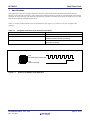
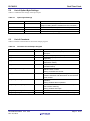
Table 1.1 lists the peripheral functions to be used and their uses. Figure 1.1 presents an overview of sample code
operation.
Table 1.1
Peripheral Functions to be Used and Their Uses
Peripheral Function
Real-time clock
P10
P11
Use
Used to generate RTC interrupts (INTRTC).
Set to a port output (inverted output) by
constant-period interrupt processing.
Set to a port output (high-level output) by alarm
interrupt processing.
P10
Constant-period interrupts
RL78/G13
Figure 1.1
P11
Alarm interrupts
Overview of Sample Code Operation
R01AN0454EJ0200
Dec. 27, 2013
Rev. 2.00
Page 3 of 29
RL78/G13
2.
Real-Time Clock
Operation Check Conditions
The sample code described in this application note has been checked under the conditions listed in the table below.
Table 2.1
Operation Check Conditions
Item
Microcontroller used
Operating frequency
Operating voltage
Integrated development
environment (CubeSuite+)
C compiler (CubeSuite+)
Integrated development
environment (e2studio)
C compiler (e2studio)
Integrated development
environment (IAR)
C compiler (IAR)
3.
Description
RL78/G13 (R5F100LEA)
• High-speed on-chip oscillator (HOCO) clock: 32 MHz
• CPU/peripheral hardware clock: 32 MHz
5.0 V (Operation is possible over a voltage range of 2.9 V to 5.5 V.)
LVD operation (VLVI): Reset mode which uses 2.81 V (2.76 V to 2.87 V)
CubeSuite+ V1.00.01 from Renesas Electronics Corp.
CA78K0R V1.20 from Renesas Electronics Corp.
e2studio V2.0.1.3 from Renesas Electronics Corp.
KPIT GNURL78-ELF Toolchain V13.02 from Renesas Electronics Corp.
IAR Embedded Workbench for Renesas RL78 V1.30.2
IAR C/C++ Compiler for Renesas RL78 V1.30.2
Related Application Note
The application note that is related to this application note is listed below for reference.
• RL78/G13 Initialization (R01AN0451EJ0100) Application Note
R01AN0454EJ0200
Dec. 27, 2013
Rev. 2.00
Page 4 of 29
RL78/G13
4.
4.1
Real-Time Clock
Description of the Hardware
Hardware Configuration Example
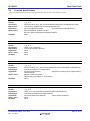
Figure 4.1 shows an example of hardware configuration that is used for this application note.
VDD
VDD
EVDD
RESET
VDD
RL78/G13
P10
Set to an inverted output by
constant-period interrupt
processing.
P11
Set to a high-level output by
alarm interrupt processing.
32.768 kHz
REGC
XT1
EVSS
VSS
XT2
P40/TOOL0
Figure 4.1
For on-chip debugger
Hardware Configuration
Cautions: 1. The purpose of this circuit is only to provide the connection outline and the circuit is simplified
accordingly. When designing and implementing an actual circuit, provide proper pin treatment and make
sure that the hardware's electrical specifications are met (connect the input-only ports separately to VDD
or VSS via a resistor).
2. Connect any pins whose name begins with EVSS to VSS and any pins whose name begins with EVDD to
VDD, respectively.
3. VDD must be held at not lower than the reset release voltage (VLVI) that is specified as LVD.
4.2
List of Pins to be Used
Table 4.1 lists the pins to be used and their functions.
Table 4.1
Pins to be Used and Their Functions
Pin Name
P10
P11
R01AN0454EJ0200
Dec. 27, 2013
I/O
Output
Output
Rev. 2.00
Description
Set to an inverted output by constant-period interrupt processing.
Set to a high-level output by alarm interrupt processing.
Page 5 of 29
RL78/G13
5.
Real-Time Clock
Description of the Software
5.1
Operation Outline
After initialization, the current date and time of the clock are set to “2010/4/1 (THU) 15:59:55” and the alarm date and
time to “16:00:00 each day” for the operations described in this application note. Also, the following interrupt
processing is performed:
• Constant-period interrupt processing for setting P10 to an inverted output
• Alarm interrupt processing for setting P11 to a high-level output
(1) Initialize the real-time clock (RTC).
< Conditions for setting>
•
•
•
•
•
•
Select the subsystem clock (fSUB) as the RTC operation clock.
Disable the RTC1HZ pin output.
Present the time in 24-hour system.
Enable RTC constant-period interrupts and set their cycle time to 0.5 second.
Initialize the current date and time to 2001/1/1 (Monday) 00:00:00.
Enable INTRTC interrupts.
(2) Configure the I/O ports.
• Configure P10 as an output port (initial value: high level) for constant-period interrupt processing.
• Configure P11 as an output port (initial value: low level) for alarm interrupt processing.
Caution: For precautions in using the device, refer to RL78/G13 User's Manual: Hardware.
R01AN0454EJ0200
Dec. 27, 2013
Rev. 2.00
Page 6 of 29
RL78/G13
5.2
Real-Time Clock
List of Option Byte Settings
Table 5.1 summarizes the settings of the option bytes.
Table 5.1
Option Byte Settings
Address
000C0H/010C0H
Value
01101110B
000C1H/010C1H
000C2H/010C2H
000C3H/010C3H
01111111B
11101000B
10000101B
5.3
Description
Disables the watchdog timer.
(Stops counting after the release from the reset state.)
LVD reset mode, 2.81 V (2.76 V to 2.87 V)
HS mode, HOCO: 32 MHz
Enables the on-chip debugger.
List of Constants
Table 5.2 lists the constants that are used in this sample program.
Table 5.2
Constants for the Sample Program
Constant
HALFSEC
Setting
1U
MD_OK
MD_ARGERROR
0x00U
0x80U
MD_BUSY1
0x03U
MD_BUSY2
0x04U
_01_RTC_COUNTER_PAUSE
0x01U
RTC_WAITTIME
320U
_80_RTC_ALARM_ENABLE
0x80U
_40_RTC_ALARM_INT_ENABLE
0x40U
_10_RTC_ALARM_MATCH
_08_RTC_INTC_GENERATE_FLAG
0x10U
0x08U
R01AN0454EJ0200
Dec. 27, 2013
Rev. 2.00
Description
Specifies the cycle time (0.5 s) for constant-period
interrupts.
Setup status (setup completed)
Setup status (setup unsuccessful due to an invalid
argument)
Setup status (setup unsuccessful due to a counter
deactivation failure)
Setup status (setup unsuccessful due to a counter
activation failure)
Specifies whether to activate or deactivate the
real-time clock counter.
Setting: Activates the counter.
Specifies the wait time (about 10 µs) after switching
between activation and deactivation of the real-time
clock counter.
Specifies whether to enable or disable alarm
operation.
Setting: Enables alarm operation.
Specifies whether to enable or disable interrupts
due to alarm matching.
Setting: Enables interrupts.
Clears the alarm detection status flag.
Clears the constant-period interrupt status flag.
Page 7 of 29
RL78/G13
5.4
Real-Time Clock
List of Functions
Table 5.3 lists the functions that are used in this sample program.
Table 5.3
Functions for the Sample Program
Function Name
R_RTC_Set_ConstPeriodInterruptOn
R_RTC_Start
R_RTC_Set_CounterValue
R_RTC_Set_AlarmValue
R_RTC_Interrupt
R_RTC_Callback_Alarm
R_RTC_Callback_ConstPeriod
R01AN0454EJ0200
Dec. 27, 2013
Rev. 2.00
Outline
Enables constant-period interrupts.
Enables the RTC.
Changes the RTC counter value.
Configures the alarm output.
Processes RTC interrupts (INTRTC).
Processes alarm interrupts.
Processes constant-period interrupts.
Page 8 of 29
RL78/G13
5.5
Real-Time Clock
Function Specifications
This section describes the specifications for the functions that are used in this sample program.
[Function Name] R_RTC_Set_ConstPeriodInterruptOn
Constant-period interrupt enable
Synopsis
r_cg_rtc.h
Header
MD_STATUS R_RTC_Set_ConstPeriodInterruptOn(enum RTCINTPeriod period)
Declaration
This function configures the constant-period interrupt.
Explanation
enum RTCINTPeriod period
: [Constant-period interrupt period]
Arguments
MD_ARGERROR: Argument invalid
Return value
MD_OK: Setup completed and operation started
None
Remarks
[Function Name] R_RTC_Start
RTC enable
Synopsis
r_cg_rtc.h
Header
void R_RTC_Start(void)
Declaration
This function enables the RTC.
Explanation
None
Arguments
None
Return value
None
Remarks
[Function Name] R_RTC_Set_CounterValue
RTC counter value change
Synopsis
r_cg_rtc.h
Header
MD_STATUS R_RTC_Set_CounterValue(struct RTCCounterValue counterwriteval)
Declaration
This function sets RTC counter values.
Explanation
struct RTCCounterValue
: [Structure for storing count register values]
Arguments
counterwriteval
MD_OK: Setup completed
Return value
Others: Setup incomplete or unsuccessful
None
Remarks
[Function Name] R_RTC_Set_AlarmValue
Alarm output setup
Synopsis
r_cg_rtc.h
Header
void R_RTC_Set_AlarmValue(struct RTCAlarmValue alarmval)
Declaration
This function configures the alarm interrupt.
Explanation
struct RTCAlarmValue alarmval
: [Alarm output conditions]
Arguments
None
Return value
None
Remarks
R01AN0454EJ0200
Dec. 27, 2013
Rev. 2.00
Page 9 of 29
RL78/G13
Real-Time Clock
[Function Name] R_RTC_Interrupt
RTC interrupt (INTRTC) processing
Synopsis
r_cg_rtc.h
Header
__interrupt void R_RTC_Interrupt(void)
Declaration
Constant-period interrupts and alarm interrupts arise from the same interrupt source
Explanation
(INTRTC). This function makes a distinction between the two types of interrupts. An
alarm interrupt triggers alarm interrupt processing. A constant-period interrupt
triggers constant-period interrupt processing.
None
Arguments
None
Return value
None
Remarks
[Function Name] R_RTC_Callback_Alarm
Alarm interrupt processing
Synopsis
r_cg_rtc.h
Header
void R_RTC_Callback_Alarm(void)
Declaration
This function sets P11 to a high-level output.
Explanation
None
Arguments
None
Return value
None
Remarks
[Function Name] R_RTC_Callback_ConstPeriod
Constant-period interrupt processing
Synopsis
r_cg_rtc.h
Header
void R_RTC_Callback_ConstPeriod(void)
Declaration
This function inverts the P10 output.
Explanation
None
Arguments
None
Return value
None
Remarks
R01AN0454EJ0200
Dec. 27, 2013
Rev. 2.00
Page 10 of 29
RL78/G13
5.6
Real-Time Clock
Flowcharts
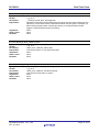
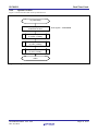
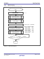
Figure 5.1 shows the overall flow of the sample program described in this application note.
Start
The option bytes are referenced before the
initialization function is called.
Initialization function
hdwinit () (Note)
Main processing
main()
End
Figure 5.1
5.6.1
Overall Flow
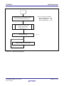
Initialization Function
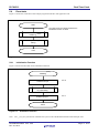
Figure 5.2 shows the flowchart for the initialization function.
(Note)
hdwinit()
Disable interrupts
IE←0
System function
R_Systeminit()
Enable interrupts
IE←1
return
Figure 5.2
Initialization Function
Note: The __low_level_init function initializes the system in the IAR Workbench IDE-Oriented sample code.
R01AN0454EJ0200
Dec. 27, 2013
Rev. 2.00
Page 11 of 29
RL78/G13
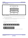
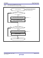
5.6.2
Real-Time Clock
System Function
Figure 5.3 shows the flowchart for the system function.
R_Systeminit()
Disuse peripheral I/O
redirection function
PIOR register ← 00000000B
Set up I/O ports
R_PORT_Create()
Set up CPU clock
R_CGC_Create()
Initialize RTC
R_RTC_Create()
return
Figure 5.3
System Function
R01AN0454EJ0200
Dec. 27, 2013
Rev. 2.00
Page 12 of 29
RL78/G13
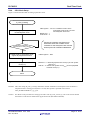
5.6.3
Real-Time Clock
I/O Port Setup
Figure 5.4 shows the flowchart for setting up the I/O ports.
R_PORT_Create()
Set P10 pin to high-level output
Set P11 pin to low-level output
Set unused pins
return
Figure 5.4
I/O Port Setup
Note: Refer to the section entitled "Flowcharts" in RL78/G13 Initialization Application Note (R01AN0451EJ0100)
for the configuration of the unused ports.
Caution: Provide proper treatment for unused pins so that their electrical specifications are observed. Connect each of
any unused input-only ports to VDD or VSS via a separate resistor.
Setting up the output pin by using real-time clock interrupts (INTRTC)
Symbol: PM1
7
6
5
4
3
2
1
0
PM17
PM16
PM15
PM14
PM13
PM12
PM11
PM10
x
x
x
x
x
x
0
0
Bits 1 and 0
PM1n
0
1
PMIn I/O mode selection (n = 0, 1)
Output mode (output buffer on)
Input mode (output buffer off)
Caution: For details on the register setup procedures, refer to RL78/G13 User's Manual: Hardware.
R01AN0454EJ0200
Dec. 27, 2013
Rev. 2.00
Page 13 of 29
RL78/G13
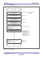
5.6.4
Real-Time Clock
CPU Clock Setup
Figure 5.5 shows the flowchart for setting up the CPU clock.
R_CGC_Create()
CMC register ← 10H: XT1 oscillation mode in which
high-speed system clock is unused
and subsystem clock used.
MSTOP bit ← 1
XTSTOP bit ← 0
Set up high-speed system
clock/subsystem clock
Oscillation stabilization
completed within waiting period?
No
Contact the oscillator manufacturer for
information about the oscillator circuit
constants for the subsystem clock and the
timeout period for oscillation stabilization.
Yes
Enable supply of subsystem clock
signals to peripheral functions
Select CPU/peripheral hardware
clock (fCLK)
OSMC register ← 00H
MCM0 bit ← 0: Select high-speed OCO clock (fIH) as main system
clock (fMAIN)
CSS bit ← 0: Selects main system clock (fMAIN) as CPU/peripheral
hardware clock (fCLK).
return
Figure 5.5
CPU Clock Setup
Remarks: CPU clock setup (R_CGC_Create()) determines whether stabilization of subsystem clock oscillation is
completed within a waiting period (about 1 second). This period is specified with constant
CGC_SUBWAITTIME in r_cg_cgc.h.
Caution: For details on the procedure for setting up the CPU clock (R_CGC_Create ()), refer to the section entitled
"Flowcharts" in RL78/G13 Initialization Application Note (R01AN0451EJ0100).
R01AN0454EJ0200
Dec. 27, 2013
Rev. 2.00
Page 14 of 29
RL78/G13
5.6.5
Real-Time Clock
RTC Initialization
Figure 5.6 shows the flowchart for RTC initialization.
R_RTC_Create
Supply clock signals to real-time
clock circuit
RTCEN bit ← 1: Starts supplying input
clock signals.
Deactivate real-time clock
RTCE bit ← 0
Clear real-time clock/alarm match
interrupt request flag
RTCIF bit ← 0
Disable real-time clock/alarm
match interrupts
Initialize real-time clock
• Set interval of constant-period interrupts to 0.5
second
• Select 24-hour system
• Disable 1-Hz output
Initialize real-time clock counter
Initialize alarm function
• Disable match operation for alarm
function
• Generate alarm interrupts
RTCMK bit ← 1
RTCC0 register ← 09H
SEC register ← 00H
MIN register ← 00H
HOUR register ← 00H
WEEK register ← 01H
DAY register ← 01H
MONTH register ← 01H
YEAR register ← 01H
WALE bit ← 0
WALIE bit ← 1
return
Figure 5.6
RTC Initialization
R01AN0454EJ0200
Dec. 27, 2013
Rev. 2.00
Page 15 of 29
RL78/G13
Real-Time Clock
Enabling supply of clock signals to the RTC
• Peripheral enable register 0 (PER0)
Enable supply of clock signals to the real-time clock.
Symbol: PER0
7
6
5
4
3
2
1
0
RTCEN IICA1EN ADCEN IICA0EN SAU1EN SAU0EN TAU1EN TAU0EN
1
0
x
x
x
x
0
x
Bit 7
Control of input clock signals to the real-time
clock
RTCEN
0
Stops input clock supply.
1
Enables input clock supply.
RTC operation control
• Real-time clock control register 0 (RTCC0)
Select a time format.
Set the interval of constant-period interrupts.
Symbol: RTCC0
7
6
5
4
3
2
1
0
RTCE
0
RCLOE1
0
AMPM
CT2
CT1
CT0
0
0
0
0
1
0
0
1
Bit 7
RTCE
0
1
Real-time clock operation control
Stops the counter operation.
Starts the counter operation.
Bit 3
AMPM
0
1
Selection of 12-/24-hour system
12-hour system (a.m. and p.m. are displayed.)
24-hour system
Bits 2 to 0
CT2
CT1 CT0
Constant-period interrupt (INTRTC) selection
0
0
0
Does not use constant-period interrupt function.
0
0
1
Once per 0.5 s (synchronized with second count up)
0
1
0
Once per 1 s (same time as second count up)
0
1
1
Once per 1 m (second 00 of every minute)
1
0
0
Once per 1 hour (minute 00 and second 00 of every hour)
1
1
0
1
1
x
Once per 1 day (hour 00, minute 00, and second 00 of every day)
Once per 1 month (Day 1, hour 00 a.m., minute 00, and second 00 of every month)
Caution: For details on the register setup procedures, refer to RL78/G13 User's Manual: Hardware.
R01AN0454EJ0200
Dec. 27, 2013
Rev. 2.00
Page 16 of 29
RL78/G13
Real-Time Clock
Specifying the date and time in the format of year, month, day, week, hour, minute and second.
• Count registers (YEAR, MONTH, DAY, WEEK, HOUR, MIN and SEC)
Specify the date and time.
Symbol: YEAR
7
6
5
4
3
2
1
0
2
1
0
00 to 99 (BCD code)
Symbol: MONTH
7
6
5
0
0
0
4
3
01 to 12 (BCD code)
Symbol: DAY
7
6
0
0
5
4
3
2
1
0
1
0
0 to 31 (BCD code)
Symbol: WEEK
7
6
5
4
3
0
0
0
0
0
5
4
3
2
0 to 6
Symbol: HOUR
7
6
0
0
2
1
0
0 to 23 or 1 to 12, 21 to 32 (BCD code)
Symbol: MIN
7
6
5
0
4
3
2
1
0
1
0
0 to 59 (BCD code)
Symbol: SEC
7
6
5
0
4
3
2
0 to 59 (BCD code)
Caution: For details on the register setup procedures, refer to RL78/G13 User's Manual: Hardware.
R01AN0454EJ0200
Dec. 27, 2013
Rev. 2.00
Page 17 of 29
RL78/G13
Real-Time Clock
Configuring the alarm interrupt generated by the real-time clock
• Real-time clock control register 1 (RTCC1)
Configure the alarm match operation.
Configure the alarm match interrupt.
Symbol: RTCC1
7
6
5
4
3
2
1
0
WALE
WALIE
0
WAFG
RIFG
0
RWST
RWAIT
0
1
0
x
x
0
x
x
Bit 7
WALE
Alarm operation control
0
Disables match operation.
1
Enables match operation.
Bit 6
WALIE
Alarm interrupt (INTRTC) function control
0
Does not generate interrupts due to an alarm match.
1
Generates interrupts due to an alarm match.
Caution: For details on the register setup procedures, refer to RL78/G13 User's Manual: Hardware.
R01AN0454EJ0200
Dec. 27, 2013
Rev. 2.00
Page 18 of 29
RL78/G13
5.6.6
Real-Time Clock
Main Processing
Figures 5.7 and 5.8 show the flowcharts for main processing.
main
Disable interrupts
IE ← 0
Reconfigure RTC
R_RTC_Set_ConstPeriodInterruptOn(HALFSEC)
Start operation of RTC
R_RTC_Start()
Disable watch error correction function
Store clock time in variable in RAM
• Thursday April 1, 2010 15:59:55
Set RTC time
R_RTC_Set_CounterValue(counter_val)
SUBCUD register ← 00000000B
counter_val: Structure variable
counter_val.Sec ← 55h
counter_val.Min
← 59h
counter_val.Hour ← 15h
counter_val.Week ← 04h
counter_val.Day
← 01h
counter_val.Month ← 04h
counter_val.Year ← 10h
Underway
Real-time clock counter setup?
Completed
1
Figure 5.7
Main Processing (1/2)
R01AN0454EJ0200
Dec. 27, 2013
Rev. 2.00
Page 19 of 29
RL78/G13
Real-Time Clock
1
Store alarm time in variable in RAM
• 16 hours 00 minutes each day
alarm_val: Structure variable
alarm_val.Alarmwm ← 00h
alarm_val.Alarmwh ← 16h
alarm_val.Alarmww ← FFh
Set alarm occurrence time
R_RTC_Set_AlarmValue( alarm_val )
Enable interrupts
IE ← 1
Make transition to HALT mode
Figure 5.8
Main Processing (2/2)
R01AN0454EJ0200
Dec. 27, 2013
Rev. 2.00
Page 20 of 29
RL78/G13
Real-Time Clock
Correcting the watch error
• Watch error correction register (SUBCUD)
Correct the watch error by incrementing or decrementing it.
Symbol: SUBCUD
7
6
5
4
3
2
1
0
DEV
F6
F5
F4
F3
F2
F1
F0
0
0
0
0
0
0
0
0
Bit 7
DEV
0
1
Setting of watch error correction timing
Corrects watch error when the second digits are at
00, 20, or 40 (every 20 seconds).
Corrects watch error only when the second digits are
at 00 (every 60 seconds).
Bit 6
F6
Setting of watch error correction value
0
Increases by {(F5, F4, F3, F2, F1, F0) − 1} × 2.
1
Decreases by {(/F5, /F4, /F3, /F2, /F1, /F0) + 1} × 2.
Caution: For details on the register setup procedures, refer to RL78/G13 User's Manual: Hardware.
R01AN0454EJ0200
Dec. 27, 2013
Rev. 2.00
Page 21 of 29
RL78/G13
5.6.7
Real-Time Clock
RTC Reconfiguration
Figure 5.9 shows the flowchart for main processing.
R_RTC_Set_Const
PeriodInterruptOn
Argument: Period
status ← MD_OK
Initialize status flag
RTC interrupt interval
normal?
status: Variable in RAM
No
No
Yes
Reconfigure real-time clock
• Set interval of constant-period interrupt to
0.5 second
• Select 24-hour system
• Disable 1-Hz output
Clear real-time clock/alarm match
interrupt request flag
Enable real-time clock/alarm match
interrupts
Set status flag to indicate error
RTCIF bit ← 0
RTCMK bit ← 0
Return status flag
return
Figure 5.9
RTC Reconfiguration
R01AN0454EJ0200
Dec. 27, 2013
Rev. 2.00
Page 22 of 29
RL78/G13
5.6.8
Real-Time Clock
RTS Startup
Figure 5.10 shows the flowchart for starting the operation of the RTC.
R_RTC_Start
Enable real-time clock interrupts
RTCIF bit ← 0: Clears interrupt request flag.
RTCMK bit ← 0: Enables interrupt processing.
Start operation of real-time clock
RTCE bit ← 1: Starts counter operation.
return
Figure 5.10
RTC Startup
R01AN0454EJ0200
Dec. 27, 2013
Rev. 2.00
Page 23 of 29
RL78/G13
Real-Time Clock
Configuring the RTC interrupt (INTRTC)
• Interrupt request flag register (IF1H)
Clear the RTCIF interrupt source flag.
• Interrupt mask flag register (MK1H)
Mask RTCMK interrupts.
Symbol: IF1H
7
6
TMIF04
TMIF13
x
x
5
4
SRIF3
STIF3
CSIIF31 CSIIF30
IICIF31 IICIF30
x
x
3
2
1
0
KRIF
ITIF
RTCIF
ADIF
x
x
0
x
Bit 1
RTCIF
0
1
Interrupt request flag
No interrupt request signal is generated
Interrupt request is generated, interrupt request status
Symbol: MK1H
7
6
5
4
TMMK04 TMMK13 SRMK3
STMK3
CSIMK31 CSIMK30
IICMK31 IICMK30
x
x
x
x
3
2
1
0
KRMK
ITMK
RTCMK
ADMK
x
x
0
x
Bit 1
RTCMK
Interrupt processing control
0
Enables interrupt processing.
1
Disables interrupt processing.
Caution: For details on the register setup procedures, refer to RL78/G13 User's Manual: Hardware.
R01AN0454EJ0200
Dec. 27, 2013
Rev. 2.00
Page 24 of 29
RL78/G13
5.6.9
Real-Time Clock
RTC Time Setup
Figures 5.11 and 5.12 show the flowcharts for setting the RTC time.
[Arguments]
counterwriteval.Sec
counterwriteval.Min
counterwriteval.Hour
counterwriteval.Week
counterwriteval.Day
counterwriteval.Month
counterwriteval.Year
R_RTC_Set_CounterValue
status ← MD_OK
Initialize status flag
status: Variable in RAM
RWAIT ←1
Real-time clock counter read/write mode
Cycle time of 32.768 kHz signals has
elapsed?
No
Yes
RTC status?
Read/write mode
Active
Set status flag to indicate error
status ← MD_BUSY1
3
Set current time
• Second count register: 55 seconds
• Minute count register: 59 minutes
• Hour count register: 15 hours
• Week count register: Thursday
• Day count register: 1st
• Month count register: April
• Year count register: 2010
SEC register ← 55H
MIN register ← 59H
HOUR register ← 15H
WEEK register ← 04H
DAY register ← 01H
MONTH register ← 04H
YEAR register ← 10H
2
Figure 5.11
RTC Time Setup (1/2)
R01AN0454EJ0200
Dec. 27, 2013
Rev. 2.00
Page 25 of 29
RL78/G13
Real-Time Clock
2
Restart real-time clock count operation
Cycle time of 32.768 kHz signals has
elapsed?
RWAIT ←0
No
Yes
Read/write mode
RTC status?
Active
Set status flag to indicate error
status ← MD_BUSY2
3
Return status flag
return
Figure 5.12
RTC Time Setup (2/2)
R01AN0454EJ0200
Dec. 27, 2013
Rev. 2.00
Page 26 of 29
RL78/G13
5.6.10
Real-Time Clock
Alarm Generation Time Setup
Figure 5.13 shows the flowchart for setting the alarm generation time.
R_RTC_Set_AlarmValue
Disable real-time clock/alarm
match interrupts
[Arguments]
alarmval.Alarmwm
alarmval.Alarmwh
alarmval.Alarmww
RTCMK bit ← 1
Disable alarm function
WALE bit ← 0
Enable alarm match interrupts
WALIE bit ← 1
Set alarm: 16:00 each day
Activate alarm function
WALE bit ← 1
WAFG bit ← 0
Clear real-time clock/alarm match
interrupt request flag
RTCIF bit ← 0
Enable real-time clock/alarm match
interrupts
RTCMK bit ← 0
return
Figure 5.13
Alarm Generation Time Setup
R01AN0454EJ0200
Dec. 27, 2013
Rev. 2.00
Page 27 of 29
RL78/G13
5.6.11
Real-Time Clock
RTC Interrupt (INTRTC) Processing
Figure 5.14 shows the flowchart for processing RTC interrupts (INTRTC).
R_RTC_Interrupt
No
Constant-period interrupts and
alarm interrupts arise from the
same interrupt source.
Alarm interrupt has occurred?
Yes
Clear alarm detection status flag
WAFG bit ← 0
Set P11 to high-level output
NO
Constant-period interrupt has
occurred?
Yes
Clear constant-period interrupt status flag
RIFG bit ← 0
Invert P10 output
return
Figure 5.14
RTC Interrupt (INTRTC) Processing
R01AN0454EJ0200
Dec. 27, 2013
Rev. 2.00
Page 28 of 29
RL78/G13
6.
Real-Time Clock
Sample Code
The sample code is available on the Renesas Electronics Website.
7.
Documents for Reference
User’s Manual:
RL78/G13 User's Manual: Hardware (R01UH0146EJ)
RL78 Family User's Manual: Software (R01US0015EJ)
The latest version can be downloaded from the Renesas Electronics website.
Technical Updates/Technical News
The latest information can be downloaded from the Renesas Electronics website.
Website and Support
Renesas Electronics Website
http://www.renesas.com/index.jsp
Inquiries
http://www.renesas.com/contact/
R01AN0454EJ0200
Dec. 27, 2013
Rev. 2.00
Page 29 of 29
RL78/G13 Real-Time Clock
REVISION HISTORY
Rev.
Date
1.00
2.00
Sep. 30, 2011
Dec. 27, 2013
Page
—
4
11
12
Description
Summary
First edition issued
Table 2.1: Added e2studio and IAR information
Added note
Figure 5.2: Fixed typo in function name
Figure 5.3: Fixed typo in function name
All trademarks and registered trademarks are the property of their respective owners.
A-1
General Precautions in the Handling of MPU/MCU Products
The following usage notes are applicable to all MPU/MCU products from Renesas. For detailed usage notes on the
products covered by this manual, refer to the relevant sections of the document as well as any technical updates that
have been issued for the products.
1. Handling of Unused Pins
Handle unused pins in accord with the directions given under Handling of Unused Pins in the manual.
The input pins of CMOS products are generally in the high-impedance state. In operation with
unused pin in the open-circuit state, extra electromagnetic noise is induced in the vicinity of LSI, an
associated shoot-through current flows internally, and malfunctions occur due to the false
recognition of the pin state as an input signal become possible. Unused pins should be handled as
described under Handling of Unused Pins in the manual.
2. Processing at Power-on
The state of the product is undefined at the moment when power is supplied.
The states of internal circuits in the LSI are indeterminate and the states of register settings and
pins are undefined at the moment when power is supplied.
In a finished product where the reset signal is applied to the external reset pin, the states of pins are
not guaranteed from the moment when power is supplied until the reset process is completed.
In a similar way, the states of pins in a product that is reset by an on-chip power-on reset function
are not guaranteed from the moment when power is supplied until the power reaches the level at
which resetting has been specified.
3. Prohibition of Access to Reserved Addresses
Access to reserved addresses is prohibited.
The reserved addresses are provided for the possible future expansion of functions. Do not access
these addresses; the correct operation of LSI is not guaranteed if they are accessed.
4. Clock Signals
After applying a reset, only release the reset line after the operating clock signal has become stable.
When switching the clock signal during program execution, wait until the target clock signal has stabilized.
When the clock signal is generated with an external resonator (or from an external oscillator) during
a reset, ensure that the reset line is only released after full stabilization of the clock signal.
Moreover, when switching to a clock signal produced with an external resonator (or by an external
oscillator) while program execution is in progress, wait until the target clock signal is stable.
5. Differences between Products
Before changing from one product to another, i.e. to one with a different part number, confirm that the
change will not lead to problems.
The characteristics of MPU/MCU in the same group but having different a different part number may
differ in terms of the internal memory capacity and layout pattern, and other factors, which can
affect the ranges of electrical characteristics, such as characteristic values, operating margins,
immunity to noise, and amount of radiated noise. When changing to products with a different part
number, implement a system-evaluation test for the given product.
Notice
1.
Descriptions of circuits, software and other related information in this document are provided only to illustrate the operation of semiconductor products and application examples. You are fully responsible for
the incorporation of these circuits, software, and information in the design of your equipment. Renesas Electronics assumes no responsibility for any losses incurred by you or third parties arising from the
use of these circuits, software, or information.
2.
Renesas Electronics has used reasonable care in preparing the information included in this document, but Renesas Electronics does not warrant that such information is error free. Renesas Electronics
3.
Renesas Electronics does not assume any liability for infringement of patents, copyrights, or other intellectual property rights of third parties by or arising from the use of Renesas Electronics products or
assumes no liability whatsoever for any damages incurred by you resulting from errors in or omissions from the information included herein.
technical information described in this document. No license, express, implied or otherwise, is granted hereby under any patents, copyrights or other intellectual property rights of Renesas Electronics or
others.
4.
You should not alter, modify, copy, or otherwise misappropriate any Renesas Electronics product, whether in whole or in part. Renesas Electronics assumes no responsibility for any losses incurred by you or
5.
Renesas Electronics products are classified according to the following two quality grades: "Standard" and "High Quality". The recommended applications for each Renesas Electronics product depends on
third parties arising from such alteration, modification, copy or otherwise misappropriation of Renesas Electronics product.
the product's quality grade, as indicated below.
"Standard": Computers; office equipment; communications equipment; test and measurement equipment; audio and visual equipment; home electronic appliances; machine tools; personal electronic
equipment; and industrial robots etc.
"High Quality": Transportation equipment (automobiles, trains, ships, etc.); traffic control systems; anti-disaster systems; anti-crime systems; and safety equipment etc.
Renesas Electronics products are neither intended nor authorized for use in products or systems that may pose a direct threat to human life or bodily injury (artificial life support devices or systems, surgical
implantations etc.), or may cause serious property damages (nuclear reactor control systems, military equipment etc.). You must check the quality grade of each Renesas Electronics product before using it
in a particular application. You may not use any Renesas Electronics product for any application for which it is not intended. Renesas Electronics shall not be in any way liable for any damages or losses
incurred by you or third parties arising from the use of any Renesas Electronics product for which the product is not intended by Renesas Electronics.
6.
You should use the Renesas Electronics products described in this document within the range specified by Renesas Electronics, especially with respect to the maximum rating, operating supply voltage
range, movement power voltage range, heat radiation characteristics, installation and other product characteristics. Renesas Electronics shall have no liability for malfunctions or damages arising out of the
use of Renesas Electronics products beyond such specified ranges.
7.
Although Renesas Electronics endeavors to improve the quality and reliability of its products, semiconductor products have specific characteristics such as the occurrence of failure at a certain rate and
malfunctions under certain use conditions. Further, Renesas Electronics products are not subject to radiation resistance design. Please be sure to implement safety measures to guard them against the
possibility of physical injury, and injury or damage caused by fire in the event of the failure of a Renesas Electronics product, such as safety design for hardware and software including but not limited to
redundancy, fire control and malfunction prevention, appropriate treatment for aging degradation or any other appropriate measures. Because the evaluation of microcomputer software alone is very difficult,
please evaluate the safety of the final products or systems manufactured by you.
8.
Please contact a Renesas Electronics sales office for details as to environmental matters such as the environmental compatibility of each Renesas Electronics product. Please use Renesas Electronics
products in compliance with all applicable laws and regulations that regulate the inclusion or use of controlled substances, including without limitation, the EU RoHS Directive. Renesas Electronics assumes
no liability for damages or losses occurring as a result of your noncompliance with applicable laws and regulations.
9.
Renesas Electronics products and technology may not be used for or incorporated into any products or systems whose manufacture, use, or sale is prohibited under any applicable domestic or foreign laws or
regulations. You should not use Renesas Electronics products or technology described in this document for any purpose relating to military applications or use by the military, including but not limited to the
development of weapons of mass destruction. When exporting the Renesas Electronics products or technology described in this document, you should comply with the applicable export control laws and
regulations and follow the procedures required by such laws and regulations.
10. It is the responsibility of the buyer or distributor of Renesas Electronics products, who distributes, disposes of, or otherwise places the product with a third party, to notify such third party in advance of the
contents and conditions set forth in this document, Renesas Electronics assumes no responsibility for any losses incurred by you or third parties as a result of unauthorized use of Renesas Electronics
products.
11. This document may not be reproduced or duplicated in any form, in whole or in part, without prior written consent of Renesas Electronics.
12. Please contact a Renesas Electronics sales office if you have any questions regarding the information contained in this document or Renesas Electronics products, or if you have any other inquiries.
(Note 1)
"Renesas Electronics" as used in this document means Renesas Electronics Corporation and also includes its majority-owned subsidiaries.
(Note 2)
"Renesas Electronics product(s)" means any product developed or manufactured by or for Renesas Electronics.
SALES OFFICES
http://www.renesas.com
Refer to "http://www.renesas.com/" for the latest and detailed information.
Renesas Electronics America Inc.
2880 Scott Boulevard Santa Clara, CA 95050-2554, U.S.A.
Tel: +1-408-588-6000, Fax: +1-408-588-6130
Renesas Electronics Canada Limited
1101 Nicholson Road, Newmarket, Ontario L3Y 9C3, Canada
Tel: +1-905-898-5441, Fax: +1-905-898-3220
Renesas Electronics Europe Limited
Dukes Meadow, Millboard Road, Bourne End, Buckinghamshire, SL8 5FH, U.K
Tel: +44-1628-651-700, Fax: +44-1628-651-804
Renesas Electronics Europe GmbH
Arcadiastrasse 10, 40472 Düsseldorf, Germany
Tel: +49-211-65030, Fax: +49-211-6503-1327
Renesas Electronics (China) Co., Ltd.
7th Floor, Quantum Plaza, No.27 ZhiChunLu Haidian District, Beijing 100083, P.R.China
Tel: +86-10-8235-1155, Fax: +86-10-8235-7679
Renesas Electronics (Shanghai) Co., Ltd.
Unit 204, 205, AZIA Center, No.1233 Lujiazui Ring Rd., Pudong District, Shanghai 200120, China
Tel: +86-21-5877-1818, Fax: +86-21-6887-7858 / -7898
Renesas Electronics Hong Kong Limited
Unit 1601-1613, 16/F., Tower 2, Grand Century Place, 193 Prince Edward Road West, Mongkok, Kowloon, Hong Kong
Tel: +852-2886-9318, Fax: +852 2886-9022/9044
Renesas Electronics Taiwan Co., Ltd.
13F, No. 363, Fu Shing North Road, Taipei, Taiwan
Tel: +886-2-8175-9600, Fax: +886 2-8175-9670
Renesas Electronics Singapore Pte. Ltd.
80 Bendemeer Road, Unit #06-02 Hyflux Innovation Centre Singapore 339949
Tel: +65-6213-0200, Fax: +65-6213-0300
Renesas Electronics Malaysia Sdn.Bhd.
Unit 906, Block B, Menara Amcorp, Amcorp Trade Centre, No. 18, Jln Persiaran Barat, 46050 Petaling Jaya, Selangor Darul Ehsan, Malaysia
Tel: +60-3-7955-9390, Fax: +60-3-7955-9510
Renesas Electronics Korea Co., Ltd.
11F., Samik Lavied' or Bldg., 720-2 Yeoksam-Dong, Kangnam-Ku, Seoul 135-080, Korea
Tel: +82-2-558-3737, Fax: +82-2-558-5141
© 2013 Renesas Electronics Corporation. All rights reserved.
Colophon 2.2