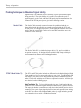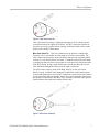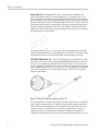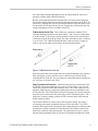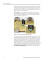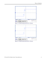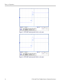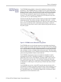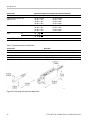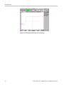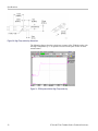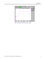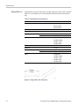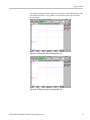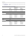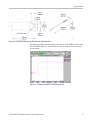
1
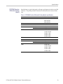
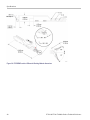
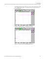
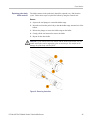
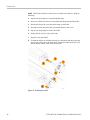
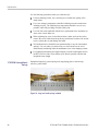
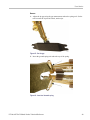
xx
ZZZ
P7504 & P7506
TriMode™ Probes
Technical Reference
*P077013500*
077-0135-00
xx
ZZZ
P7504 & P7506
TriMode™ Probes
Technical Reference
www.tektronix.com
077-0135-00
Copyright © Tektronix. All rights reserved. Licensed software products are owned by Tektronix or its subsidiaries
or suppliers, and are protected by national copyright laws and international treaty provisions.
Tektronix products are covered by U.S. and foreign patents, issued and pending. Information in this publication
supersedes that in all previously published material. Specifications and price change privileges reserved.
TEKTRONIX and TEK are registered trademarks of Tektronix, Inc.
TriMode is a trademark of Tektronix, Inc.
Velcro is a registered trademark of Velcro Industries B.V.
G3PO is a trademark of Corning Gilbert Inc.
Contacting Tektronix
Tektronix, Inc.
14200 SW Karl Braun Drive
P.O. Box 500
Beaverton, OR 97077
USA
For product information, sales, service, and technical support:
In North America, call 1-800-833-9200.
Worldwide, visit www.tektronix.com to find contacts in your area.
Warranty
Tektronix warrants that this product will be free from defects in materials and workmanship for a period of one (1)
year from the date of shipment. If any such product proves defective during this warranty period, Tektronix, at its
option, either will repair the defective product without charge for parts and labor, or will provide a replacement
in exchange for the defective product. Parts, modules and replacement products used by Tektronix for warranty
work may be new or reconditioned to like new performance. All replaced parts, modules and products become
the property of Tektronix.
In order to obtain service under this warranty, Customer must notify Tektronix of the defect before the expiration of
the warranty period and make suitable arrangements for the performance of service. Customer shall be responsible
for packaging and shipping the defective product to the service center designated by Tektronix, with shipping
charges prepaid. Tektronix shall pay for the return of the product to Customer if the shipment is to a location within
the country in which the Tektronix service center is located. Customer shall be responsible for paying all shipping
charges, duties, taxes, and any other charges for products returned to any other locations.
This warranty shall not apply to any defect, failure or damage caused by improper use or improper or inadequate
maintenance and care. Tektronix shall not be obligated to furnish service under this warranty a) to repair damage
resulting from attempts by personnel other than Tektronix representatives to install, repair or service the product;
b) to repair damage resulting from improper use or connection to incompatible equipment; c) to repair any damage
or malfunction caused by the use of non-Tektronix supplies; or d) to service a product that has been modified or
integrated with other products when the effect of such modification or integration increases the time or difficulty
of servicing the product.
THIS WARRANTY IS GIVEN BY TEKTRONIX WITH RESPECT TO THE PRODUCT IN LIEU OF ANY
OTHER WARRANTIES, EXPRESS OR IMPLIED. TEKTRONIX AND ITS VENDORS DISCLAIM ANY
IMPLIED WARRANTIES OF MERCHANTABILITY OR FITNESS FOR A PARTICULAR PURPOSE.
TEKTRONIX’ RESPONSIBILITY TO REPAIR OR REPLACE DEFECTIVE PRODUCTS IS THE SOLE
AND EXCLUSIVE REMEDY PROVIDED TO THE CUSTOMER FOR BREACH OF THIS WARRANTY.
TEKTRONIX AND ITS VENDORS WILL NOT BE LIABLE FOR ANY INDIRECT, SPECIAL, INCIDENTAL,
OR CONSEQUENTIAL DAMAGES IRRESPECTIVE OF WHETHER TEKTRONIX OR THE VENDOR HAS
ADVANCE NOTICE OF THE POSSIBILITY OF SUCH DAMAGES.
[W2 – 15AUG04]
Table of Contents
General Safety Summary ..........................................................................................
Preface .............................................................................................................
Products Covered ............................................................................................
Theory of Operation................................................................................................
Input Voltage Limits ...........................................................................................
TriMode Operation ............................................................................................
Probing Techniques to Maximize Signal Fidelity ..........................................................
Input Impedance and Probe Loading .......................................................................
Reference ...........................................................................................................
Single-Ended Measurements Using A and B Modes .....................................................
Differential Measurements...................................................................................
Serial Bus Standards..........................................................................................
Specifications ......................................................................................................
Warranted Characteristics....................................................................................
Typical Characteristics .......................................................................................
Nominal Characteristics......................................................................................
Tip Specifications .............................................................................................
User Service ........................................................................................................
Error Conditions ..............................................................................................
Replaceable Parts .............................................................................................
Preparation for Shipment ....................................................................................
P7504 & P7506 TriMode Probes Technical Reference
v
vii
vii
1
1
4
6
16
19
19
21
23
24
24
25
27
28
43
43
44
56
i
Table of Contents
List of Figures
Figure 1: Operating voltage window .............................................................................
Figure 2: Dynamic range versus linearity, 5X range ...........................................................
Figure 3: Dynamic range versus linearity, 12.5X range........................................................
Figure 4: TriMode input structure ................................................................................
Figure 5: Typical TriMode Probe Setup screen ................................................................
Figure 6: High Temp solder tip ...................................................................................
Figure 7: Micro-Coax solder tip ..................................................................................
Figure 8: P75TLRST TriMode Long Reach Solder Tip........................................................
Figure 9: TriMode Resistor solder tips...........................................................................
Figure 10: Typical wire length from probe tip to circuit ......................................................
Figure 11: P75TLRST solder tip with 0.010 in. of tip wire ..................................................
Figure 12: P75TLRST solder tip with 0.050 in. of tip wire ..................................................
Figure 13: P75TLRST solder tip with 0.100 in. of tip wire ..................................................
Figure 14: P75TLRST solder tip with 0.200 in. of tip wire ..................................................
Figure 15: P75PDPM Precision Differential Probing Module ...............................................
Figure 16: P75PDPM with short ground spring, 0.030 in. spacing..........................................
Figure 17: P75PDPM with short ground spring, 0.050 in. spacing..........................................
Figure 18: P75PDPM with short ground spring, 0.090 in. spacing..........................................
Figure 19: P75PDPM with short ground spring, 0.180 in. spacing..........................................
Figure 20: TriMode probe input model .........................................................................
Figure 21: TriMode probe high frequency input impedance model .........................................
Figure 22: Embedded probe fixture .............................................................................
Figure 23: Typical channel isolation for P7500 Series TriMode probes ....................................
Figure 24: Simplified model of a differential amplifier .......................................................
Figure 25: Typical CMRR for P7500 Series TriMode probes ................................................
Figure 26: Probe body and control box dimensions ...........................................................
Figure 27: Micro-Coax solder tip dimensions..................................................................
Figure 28: P7504 probe with the Micro-Coax solder tip......................................................
Figure 29: P7506 probe with the Micro-Coax solder tip......................................................
Figure 30: High Temp solder tip dimensions...................................................................
Figure 31: P7504 probe with the High Temp solder tip .......................................................
Figure 32: P7506 probe with the High Temp solder tip .......................................................
Figure 33: Damped Wire Pair dimensions......................................................................
Figure 34: P7504 probe with the Damped Wire Pair ..........................................................
Figure 35: P7506 probe with the Damped Wire Pair ..........................................................
Figure 36: P75TLRST TriMode Long Reach Solder Tip dimensions .......................................
Figure 37: P7504 probe with the P75TLRST solder tip.......................................................
Figure 38: P7506 probe with the P75TLRST solder tip.......................................................
ii
2
3
3
5
5
7
7
8
9
10
11
11
12
12
13
14
14
15
15
16
16
17
20
21
22
26
29
29
30
32
32
33
34
35
35
37
37
38
P7504 & P7506 TriMode Probes Technical Reference
Table of Contents
Figure 39:
Figure 40:
Figure 41:
Figure 42:
Figure 43:
Figure 44:
Figure 45:
Figure 46:
Figure 47:
Figure 48:
Figure 49:
Figure 50:
Figure 51:
Figure 52:
Figure 53:
Figure 54:
Figure 55:
Figure 56:
Figure 57:
P75PDPM Precision Differential Probing Module dimensions .................................
P7504 probe with the P75PDPM probing module ................................................
P7506 probe with the P75PDPM probing module ................................................
Removing the bullets.................................................................................
Installing the bullets ..................................................................................
Large and small springs installed ...................................................................
Set the gap.............................................................................................
Insert tool beneath spring ............................................................................
Transfer spring from tip to tool .....................................................................
Place spring on tool ..................................................................................
Set spring in front seat ...............................................................................
Set the spring in the rear seats.......................................................................
Properly seated spring................................................................................
Disconnecting the tip cable..........................................................................
Probing module tips ..................................................................................
Removing the tip .....................................................................................
Separating the tip board pair ........................................................................
Seating the tip in the top tabs........................................................................
Snapping the tip into the bottom tabs ..............................................................
P7504 & P7506 TriMode Probes Technical Reference
40
41
41
45
46
48
49
49
50
51
51
52
52
53
53
54
54
55
55
iii
Table of Contents
List of Tables
Table i: TriMode probes .........................................................................................
Table 1: Offset ranges.............................................................................................
Table 2: Serial bus standards with dynamic range requirements .............................................
Table 3: Warranted electrical characteristics ...................................................................
Table 4: Typical electrical characteristics.......................................................................
Table 5: Typical mechanical characteristics ....................................................................
Table 6: Nominal electrical characteristics .....................................................................
Table 7: Micro-Coax solder tip specifications..................................................................
Table 8: High Temp solder tip specifications...................................................................
Table 9: Damped Wire Pair specifications ......................................................................
Table 10: P75TLRST TriMode Long Reach Solder Tip specifications......................................
Table 11: P75PDPM Precision Differential Probing Module specifications ...............................
Table 12: TriMode probes replaceable parts....................................................................
Table 13: Required equipment ...................................................................................
iv
vii
19
23
24
25
26
27
28
31
34
36
39
44
44
P7504 & P7506 TriMode Probes Technical Reference
General Safety Summary
General Safety Summary
Review the following safety precautions to avoid injury and prevent damage to
this product or any products connected to it.
To avoid potential hazards, use this product only as specified.
Only qualified personnel should perform service procedures.
While using this product, you may need to access other parts of a larger system.
Read the safety sections of the other component manuals for warnings and
cautions related to operating the system.
To Avoid Fire or Personal
Injury
Connect and Disconnect Properly. Connect the probe output to the measurement
instrument before connecting the probe to the circuit under test. Connect the
probe reference lead to the circuit under test before connecting the probe input.
Disconnect the probe input and the probe reference lead from the circuit under test
before disconnecting the probe from the measurement instrument.
Observe All Terminal Ratings. To avoid fire or shock hazard, observe all ratings
and markings on the product. Consult the product manual for further ratings
information before making connections to the product.
Do not apply a potential to any terminal, including the common terminal, that
exceeds the maximum rating of that terminal.
Do Not Operate Without Covers. Do not operate this product with covers or panels
removed.
Do Not Operate With Suspected Failures. If you suspect that there is damage to this
product, have it inspected by qualified service personnel.
Avoid Exposed Circuitry. Do not touch exposed connections and components
when power is present.
Do Not Operate in Wet/Damp Conditions.
Do Not Operate in an Explosive Atmosphere.
Keep Product Surfaces Clean and Dry.
P7504 & P7506 TriMode Probes Technical Reference
v
General Safety Summary
Terms in this Manual
These terms may appear in this manual:
WARNING. Warning statements identify conditions or practices that could result
in injury or loss of life.
CAUTION. Caution statements identify conditions or practices that could result in
damage to this product or other property.
Symbols and Terms on the
Product
These terms may appear on the product:
DANGER indicates an injury hazard immediately accessible as you read
the marking.
WARNING indicates an injury hazard not immediately accessible as you
read the marking.
CAUTION indicates a hazard to property including the product.
The following symbol(s) may appear on the product:
vi
P7504 & P7506 TriMode Probes Technical Reference
Preface
This manual discusses topics that are not covered in depth in the P7504 & P7506
TriMode Probes Quick Start User Manual.
The main sections are:
Theory of Operation — Contains probe details not covered in the user manual.
Reference — Contains information about differential measurements and how
to increase measurement accuracy.
Specifications — Contains warranted, typical, and nominal characteristics for
the probe and probe tip accessories.
User Service — Describes troubleshooting and probe maintenance.
Products Covered
The table below lists the TriMode probes covered by this manual.
Table i: TriMode probes
Probe model
Serial number
P7504
All
P7506
All
P7504 & P7506 TriMode Probes Technical Reference
vii
Preface
viii
P7504 & P7506 TriMode Probes Technical Reference
Theory of Operation
This section discusses operating considerations and probing techniques. For more
detailed information about differential measurements and TriMode operation,
refer to Reference. (See page 19.)
The P7500 Series TriMode probes are optimized for high bandwidth; they
are not general-purpose probes. The probe tips are miniaturized for electrical
characteristics and access to dense circuitry, and must be handled carefully.
CAUTION. To prevent damage to the probe, use care when handling the probe.
Rough or careless use can damage the probe.
Input Voltage Limits
The P7500 Series TriMode probes are designed to probe low-voltage circuits.
Before probing a circuit, take into account the limits for maximum input voltage,
the operating voltage window, and the differential-mode signal range. (See
Table 4 on page 25.)
Maximum Input Voltage
The maximum input voltage is the maximum voltage to ground that the inputs can
withstand without damaging the probe input circuitry.
CAUTION. To avoid damaging the inputs of the probes, do not apply more than
±15 V (DC + peak AC) between each input or between either probe input and
ground.
CAUTION. To avoid ESD (electrostatic discharge) damage to the probe, always
use an antistatic wrist strap and work at a static-approved workstation when
you handle the probe.
P7504 & P7506 TriMode Probes Technical Reference
1
Theory of Operation
Operating Voltage Window
The operating voltage window defines the maximum voltage that you can apply
to each input, with respect to earth ground, without saturating the probe input
circuitry. A common-mode voltage that exceeds the operating voltage window
may produce an erroneous output waveform even when the differential-mode
specification is met.
Figure 1: Operating voltage window
Differential-Mode Signal
Range
Offset Voltage Range
2
The differential-mode signal range is the maximum voltage difference between
the A and B inputs that the probe can accept without distorting the signal. The
distortion from a voltage that exceeds this maximum can result in a clipped or
otherwise inaccurate measurement. The P7500 Series probes have two attenuation
settings, 5X and 12.5X, that allow dynamic range to be traded off against signal
noise. The 12.5X attenuator setting has the largest dynamic range; the 5X
attenuator setting has the lowest noise. The graphs on the following pages
illustrate the linearity error over the dynamic voltage range of the probes in both
attenuation settings.
The Offset Voltage Control, accessible from the attached oscilloscope user
interface, allows the probe dynamic range to be effectively moved up and down
within the limits of the offset voltage range and the operating voltage window.
When the offset voltage is set to zero volts and the input signal is zero volts
(inputs shorted to ground, not open), the displayed signal should be zero volts.
If a noticeable zero volt offset is present under the above conditions, a Probe
Cal operation should be performed. (See the P7500 Series Probes Quick Start
User Manual).
P7504 & P7506 TriMode Probes Technical Reference
Theory of Operation
Figure 2: Dynamic range versus linearity, 5X range
Figure 3: Dynamic range versus linearity, 12.5X range
P7504 & P7506 TriMode Probes Technical Reference
3
Theory of Operation
TriMode Operation
The TriMode feature of the new P7500 Series probe family is designed for
improved convenience and enhanced capability in measuring differential
signal quality. Since a differential signal is composed of two complementary
single-ended signals, full characterization of differential signal quality requires
more than a simple differential measurement. A TriMode probe features three
Input Modes that allow a differential signal to be fully characterized with four
measurements: differential, positive polarity and negative polarity single-ended,
and common mode.
A TriMode probe provides improved efficiency and convenience by enabling full
differential signal characterization from a single soldered connection. Using one
of the solder tips available for the TriMode probes, (for example, the P75TLRST
probe tip), probe connections are soldered to the two complementary signals (the
A signal and the B signal) and a ground reference. From this single DUT (device
under test) connection, the internal electronic switching control of the TriMode
probe allows any one of the three probe Input Modes (four measurements) to
be selected at a time. The TriMode probe inputs are routed on the probe ASIC
(application-specific integated circuit) to a set of four independent input amplifiers
that perform the following signal calculations:
A – B (for differential signal measurement)
A – GND (for positive polarity single-ended measurement)
B – GND (for negative polarity single-ended measurement)
[A+B]/2 - GND (for common mode measurement)
NOTE. In the B – GND Mode, the negative polarity B input is not inverted.
The four input amplifiers are multiplexed together and only the selected Input
Mode function is output to the connected oscilloscope. (See Figure 4 on page 5.)
The figure shows a conceptual view of the TriMode probe input structure, where
the C input provides the probe ground reference and is connected to the probe tip
ground interconnect using the probe tip cable coaxial shields.
4
P7504 & P7506 TriMode Probes Technical Reference
Theory of Operation
Figure 4: TriMode input structure
On oscilloscopes that do not provide full TriMode support, the TriMode features
are controlled by the probe Control Box switches, which allow oscilloscope
features like Probe Cal to be exercised only for the selected probe Input Mode.
On oscilloscopes that provide full TriMode support, the oscilloscope-controlled
probe GUI (graphical-user interface) can perform a Probe Cal operation on all
Input Modes and Attenuation Settings at once using the TriMode Probe Cal fixture
that is supplied with P7500 Series probes. (See the P7500 Series Quick Start
User Manual for instructions on running the Probe Cal routine.) Full TriMode
support will also allow storage and automatic recall of relevant settings like
Offset. (See Figure 5.)
Figure 5: Typical TriMode Probe Setup screen
P7504 & P7506 TriMode Probes Technical Reference
5
Theory of Operation
Probing Techniques to Maximize Signal Fidelity
Signal fidelity is an indication of how accurately a probe represents the signal
being measured. The signal fidelity of the probe is best when the probe is
applied properly to the circuit with the P7500 probe tips. Recommendations for
connecting the P7500 probe tips are given in the following section.
Socket Cables
The Socket Cable assembly connects between the probe head and the two
leave-behind probe tips that ship as standard accessories with the P7504 and
P7506 probes. It is designed to preserve a 50 Ω signal path from the input to the
probe, down the coaxial cable, and as well as possible through the square-pin
connection to the solder tips.
The Socket Cable XL is a similar but longer cable (5 ft.), and is available as
an optional accessory. It is designed for use with the High Temp solder tip in
environmental test chambers and similar applications.
P7500 TriMode Solder Tips
The P7504 and P7506 probes include two different leave-behind solder tips (High
Temp and Micro-Coax) to connect the probes to your circuit. Two High Temp and
four Micro-Coax probe tips are shipped with the probes as standard accessories;
other P7500 Series solder tips are available as optional accessories. All of the tips
are described on the following pages.
High Temp Solder Tip. This leave-behind probe tip uses a 3-pin header with two
connections for a differential signal and a third connection for a ground reference.
The square pin header is mounted on a small circuit board which provides circuit
connections for a pair of input signal pickoff resistors and a ground via for wiring
to the DUT. As shown in the illustration, this probe tip design includes a ground
via at the probe tip to provide a TriMode connection.
6
P7504 & P7506 TriMode Probes Technical Reference
Theory of Operation
Figure 6: High Temp solder tip
This 3-pin interface topology is signal-ground-signal (S-G-S) with the ground
connection between the signals for isolation. The DUT connection interface at
the probe tip vias uses a split-resistor topology with axial-leaded resistors rather
than wires for the DUT interconnect.
Micro-Coax Solder Tip. This leave-behind probe tip includes a mating cable
assembly with a 3-pin header for connecting to one of the socket cables. The
cable connection between the square-pin header and the probe tip signal pickoff
resistors is a very flexible micro-coax cable. A TriMode connection can be made
by adding a ground wire between a ground via on the probe tip circuit board and a
local DUT ground, giving a single-ended return current path along the coaxial
cable shield and through the center pin of the square-pin header.
The split-resistor topology used on the High Temp tip is also used on the
Micro-Coax tip, as shown in the illustration. Replaceable axial-leaded resistors
located at the probe tip are used for DUT connections, and surface-mount resistors
are set back on the probe tip interface board. The square-pin header connector on
the interface circuit board of the Micro-Coax solder tip is shielded with a ground
shield similar to that used on the mating Socket Cable.
Figure 7: Micro-Coax solder tip
P7504 & P7506 TriMode Probes Technical Reference
7
Theory of Operation
Damped Wire Tip. The Damped Wire Tip is a non-coaxial, extended-reach
probe tip designed for DUT interconnect flexibility. The primary focus is for a
single-ended probe tip solution with independent signal and ground connections.
By separating the signal and ground connections, the user can provide a common
ground connection for a group of different signal connections. This tip reduces the
interconnect soldering task for applications with many single-ended signals and
may have adequate performance for slower-speed signals. When routed closer
together for a differential measurement, the damped wire tip provides remarkably
good high frequency performance.
The Damped Wire Tip has a 1.7 inch reach, which is designed for use in DDR
memory module applications. The performance is optimized by splitting the input
signal pickoff resistor as is done with the High Temp and Micro-Coax tips.
P75TLRST TriMode Solder Tip. The P75TLRST probe tip is composed of a small
form factor interconnect circuit board with SMD0402 damping resistors and a set
of vias for wire attachment to the DUT (Device Under Test). The circuit board
vias are designed for both 4 mil and 8 mil wire and a special high tensile strength
wire is supplied as part of the wire accessory kit. The expanded view of the probe
tip shows the location of the A and B signal inputs as well as the two ground
reference connections.
Figure 8: P75TLRST TriMode Long Reach Solder Tip
The recommended wire attachment method is to first solder the wires to the DUT,
being careful to minimize the wire length of the signal and ground connections.
This is followed by threading the wires through the probe tip board vias, being
careful to achieve as symmetrical a wire pattern as possible between the two
signal inputs and a very short ground connection. Finally, the attachment is
completed by soldering the wires on top of the probe tip circuit board. Any excess
8
P7504 & P7506 TriMode Probes Technical Reference
Theory of Operation
wire lead length extending through the probe tip board should be removed to
minimize possible signal reflection problems.
Because of the limited mechanical strength of the wire interconnect and probe
tip circuit board, the solder-down probe tip should be taped down at the DUT for
strain relief. Although the accessory kit includes adhesive strips that can be used
for the strain relief of the probe tip, the use of mylar tape will generally provide
stronger attachment if room is available at the DUT.
TriMode Resistor Solder Tips. These solder tips separate the standard 175 Ω
on-board damping resistors for each probe input (+ and –) into two components.
A surface mount, 75 Ω resistor is board-mounted in series with a 100 Ω leaded
resistor that extends off of the tip board. The other end of the resistor is soldered
to your circuit. The TriMode Extended Resistor solder tips allow a longer tip
reach to your circuit under test but reduce the measurement quality.
Figure 9: TriMode Resistor solder tips
Since the leads of the 100 Ω resistors take the repeated soldering cycles required
when reusing the tip, they limit the need to solder directly to the tip board,
extending the life of the tip. The tip resistors are replaceable and are available as a
kit. (See page 44, Replaceable Parts.)
Probe Tip Cables and Connectors. Attached to the probe tip circuit board of the
P75TLRST and resistor solder tips are a pair of very low skew (<1ps) coaxial
cables and a polarized G3PO dual connector block. The G3PO connectors use a
miniature, high frequency design that enables quick and easy installation of the
P7500 probe tips. The G3PO connector block of the probe tip is inserted into the
input nose piece on the end of the probe body of the P7500 family probes. The
probe body contains a mating, polarized G3PO connector block with attached
G3PO connector bullets.
The connector bullets are a part of the G3PO connector design, providing a
self-aligning interconnect mechanism between G3PO connectors. The G3PO
connector in the probe body is designed to have higher detent force than the probe
tip connectors, which is intended to ensure that the G3PO bullets remain in the
probe body connector when disconnected. The probe body nose piece, with its
integral spring mechanism, helps to provide a self-aligning mechanism for hand
P7504 & P7506 TriMode Probes Technical Reference
9
Theory of Operation
insertion of the probe tip. The probe body nose springs also give a secure capture
of the probe tip connector after insertion. Release of the probe tip is assisted by
using the wire-connected cable release holder on the probe tip connector. This
probe tip release holder should always be used rather than pulling on the probe tip
cables, which may cause tip cable damage.
DUT Connections. The lead length of the resistor leads and connection wires
between the probe tip board and the DUT must be kept as short as possible to
preserve the integrity of the measured signal. Typical wire lengths range from
0.010 in. to 0.100 in. (See Figure 10.)
Figure 10: Typical wire length from probe tip to circuit
The following four figures illustrate the signal integrity effect on the P75TLRST
solder tip when used with different lengths of tip wire. Signal fidelity is best when
the wire length is kept as short as possible. The step generator that was used as
a signal source for these screenshots has a 30 ps 10-90% rise time. The table in
each figure contains data for two rise time measurements (10-90% and 20-80%)
and were made using a P7516 probe. Comparable measurements made using a
P7504 or P7506 probe would show much slower rise times.These screenshots can
be used as a rough guide to gauge the effects of wire length, but actual results may
vary depending on the other factors like characteristics of the device under test
(for example, rise time and impedance), precision of the solder connection, and
the model of probe and oscilloscope.
10
P7504 & P7506 TriMode Probes Technical Reference
Theory of Operation
Figure 11: P75TLRST solder tip with 0.010 in. of tip wire
Figure 12: P75TLRST solder tip with 0.050 in. of tip wire
P7504 & P7506 TriMode Probes Technical Reference
11
Theory of Operation
Figure 13: P75TLRST solder tip with 0.100 in. of tip wire
Figure 14: P75TLRST solder tip with 0.200 in. of tip wire
12
P7504 & P7506 TriMode Probes Technical Reference
Theory of Operation
P75PDPM Precision
Differential Probing
Module
The P75PDPM Probing Module is designed for handheld and fixtured probing
applications. The P75PDPM probe tip is composed of two replaceable probe tip
circuit boards with a pin on one end and a G3PO socket connector on the other.
Damping resistors on the tip boards near the input pins and a 50 Ω transmission
line on the board transmit the signal from the input pin to the G3PO socket
connector. The probe tip boards are connected to the P7500 probe body with a
very low skew (<1 ps) cable assembly (P75TC).
The left-side and right-side probe tip boards mount at an angle in the P75PDPM
adjustment housing. The probe tip spacing is adjustable from 0.030 – 0.180 in.
(0.76 – 4.57 mm) using the thumb-operated screw. Because of the variable spacing
between the two probe tip boards, a gold-plated ground spring is connected
between the probe tip boards to ensure a good common mode ground return near
the probe tip pins.
Figure 15: P75PDPM Precision Differential Probing Module
The P75PDPM probe tip circuit boards mount in an articulating metal housing
that also supports the variable spacing control. The angle of the probe tip housing
can be adjusted and locked in place using an articulation screw in the probe holder
bar. The probe holder bar contains mechanical details for retaining the probe tip
cable assembly as well as a retaining clamp for the probe body. The probe holder
bar can be held manually or can be mounted for fixtured probing on an articulating
probe arm using mechanical features in the holder bar.
The P75PDPM design features improved mechanical compliance in probe
tip attachment to the DUT. Mechanical compliance is a significant issue for
differential probes because of the difficulty in making reliable contact with two
DUT connections at the same time. The reliability in making this dual point
connection can be improved by a tip structure with good mechanical compliance,
in which there is sufficient give in the probe tips to absorb interconnect surface
irregularity.
The P75PDPM does not have a local DUT ground connection because of the
great difficulty in making a good three-point interconnect without soldering. As a
result, the only low-noise TriMode Input Mode available with the P75PDPM is
the A-B (DIFF) mode, since for differential signals, there is an inherent virtual
ground present in the measurement circuit.
P7504 & P7506 TriMode Probes Technical Reference
13
Theory of Operation
The following four figures illustrate the signal integrity effect of changing the
spacing on the P75PDPM Probing Module. Signal fidelity is best with the tips at
the smallest spacing. The step generator that was used as a signal source for these
screenshots has a 30ps 10-90% rise time. The table in each figure contains data for
two rise time measurements (10-90% and 20-80%). These screenshots can be used
as a rough guide to gauge the effects of probe tip spacing, but actual results may
vary depending on the other factors like characteristics of the device under test
(for example, rise time and impedance) and the model of probe and oscilloscope.
Figure 16: P75PDPM with short ground spring, 0.030 in. spacing
Figure 17: P75PDPM with short ground spring, 0.050 in. spacing
14
P7504 & P7506 TriMode Probes Technical Reference
Theory of Operation
Figure 18: P75PDPM with short ground spring, 0.090 in. spacing
Figure 19: P75PDPM with short ground spring, 0.180 in. spacing
P7504 & P7506 TriMode Probes Technical Reference
15
Theory of Operation
Input Impedance and Probe Loading
When you connect the probe inputs to a circuit, you are introducing a new
resistance, capacitance, and inductance into the circuit. Each input of the
differential probe has a DC input impedance of 50 kΩ to ground. (See Figure 20.)
Figure 20: TriMode probe input model
For signals with low source impedance and frequency, the 50 kΩ input impedance
on each input is large enough to prevent the inputs from loading the signal
sources. The more the signal source impedance on an input increases, the more
the probe loads the source and reduces the signal amplitude. The greater the
source impedances and the higher the signal frequencies, the more you must
take these factors into account.
The frequency of the signal also affects signal measurement. As the frequency of
the signal increases, the input impedance of the probe decreases. The lower the
impedance of the probe relative to that of the source, the more the probe loads
the circuit under test and reduces the signal amplitude. A high frequency input
impedance model is shown below. (See Figure 21.)
Figure 21: TriMode probe high frequency input impedance model
For impedance values of the individual TriMode solder tips, refer to the
specifications. (See page 28, Tip Specifications.)
16
P7504 & P7506 TriMode Probes Technical Reference
Theory of Operation
Embedded Probe
It is possible to acquire signals with the P7500 Series TriMode probes by including
an embedded connection in your circuit. (See Figure 22.) Connectors that mate to
the P75TC Tip Cable can be incorporated in the circuit board design and carefully
placed to balance any reflections or other characteristics that may affect the
circuit or measurement. An embedded probe connection will generally provide
optimum probe performance because the signal interconnect lead length can be
minimized if implemented correctly. For more information about embedded probe
connections, contact Tektronix.
Figure 22: Embedded probe fixture
P7504 & P7506 TriMode Probes Technical Reference
17
Theory of Operation
18
P7504 & P7506 TriMode Probes Technical Reference
Reference
This section contains information about taking measurements with the TriMode
probes and increasing measurement accuracy.
Single-Ended Measurements Using A and B Modes
A differential probe such as the P7516 TriMode Probe can be used for
single-ended measurements within the limits of its dynamic and offset voltage
ranges. Single-ended probes such as the P7240 typically have a wider offset
range than differential probes, but generally with lower bandwidth performance.
(See Table 1.)
Table 1: Offset ranges
Probe
Frequency
DC Offset,
5X
Dynamic Range,
5X
P7240
4 GHz
+/- 5 V
P7504 & P7506
(differential mode)
4 GHz & 6 GHz
P7504 & P7506
(single-ended and
common-mode)
4 GHz & 6 GHz
Dynamic Range,
12.5X
4 VPP
DC Offset,
12.5X
–
—
+2.5 V, -1.5 V
1.5 VPP
+2.5 V, -1.5 V
3.5 VPP
+3.4 V, -1.8 V
1.5 VPP
+3.4 V, -1.8 V
3.5 VPP
Differential probes are ideal for a class of single-ended measurements where the
reference voltage is not ground:
SSTL_1,2: VTT, VREF = VDD/2
PECL: VREF = VCC-1.3
To measure single-ended signals in this class, connect the B input of the P7500
TriMode Probe to VREF.
A differential probe in these applications displays the true signal despite any AC
or DC variation in VREF from its nominal value. A single-ended probe displays
the signal plus the variation in VREF.
Differential probes can also be used to make ground referenced single-ended
measurements on either single-ended signals or differential signals like PCI
Express or Serial ATA. To measure ground referenced single-ended signals with
the handheld module, connect the B input of the P7500 TriMode Probe to ground.
Single-ended measurements on differential signals are used to measure common
mode voltage and check for differential signal symmetry. By using the TriMode
solder tip, you can easily take these measurements with one connection. Cycle the
Input Mode switch to display the signal that you want to view.
P7504 & P7506 TriMode Probes Technical Reference
19
Reference
Channel Isolation
Under ideal conditions when taking single-ended measurements with a differential
probe, no part of a signal applied to one input of the probe would appear on the
other input. In reality some portion of the signal on one input does “bleed” over to
the other input, and this effect increases with frequency. Channel isolation is a
measure of how much crosstalk occurs between the two probe inputs. The channel
isolation is defined with S-parameter measurements below, where:
A input = S1, B input = S2, Output = S3
A ISOLATION = 20 log (S32 / S31) | A Mode
B ISOLATION = 20 log (S31 / S32) | B Mode
A typical isolation plot for the P7500 series TriMode probes using an embedded
probe with zero-ground lead length is shown. Channel isolation performance is
highly dependent on probe tip attachment lead length. Good channel isolation
requires keeping the interconnect lead length for both signal and ground
connections very short. (See Figure 23.)
Figure 23: Typical channel isolation for P7500 Series TriMode probes
20
P7504 & P7506 TriMode Probes Technical Reference
Reference
Differential Measurements
A differential probe is optimized to measure high speed differential signals.
Differential signals are formed from two complementary signals with a common
reference voltage. (See Figure 24.)
Devices designed for differential measurements avoid problems presented by
single-ended systems. These devices include a variety of differential probes,
differential amplifiers, and isolators.
A differential probe is basically a differential amplifier, which is used to make
differential measurements that reject any voltage that is common to the inputs and
amplifies any difference between the inputs. Voltage that is common to both
inputs is often referred to as the Common-Mode Voltage (VCM) and voltage that
is different as the Differential-Mode Voltage (VDM).
Figure 24: Simplified model of a differential amplifier
Common-Mode Rejection
Ratio
Differential amplifiers cannot reject all of the common-mode signal. The ability
of a differential amplifier to reject the common-mode signal is expressed as the
Common-Mode Rejection Ratio (CMRR). The CMRR is the differential-mode
gain (ADM) divided by the common-mode gain (ACM). It is expressed either as
a ratio or in dB.
CMRR generally is highest (best) at DC and degrades with increasing frequency.
A typical CMRR plot for the P7500 Series TriMode probes is shown. (See
Figure 25 on page 22.)
P7504 & P7506 TriMode Probes Technical Reference
21
Reference
Figure 25: Typical CMRR for P7500 Series TriMode probes
Assessing CMRR Error
The CMRR of the P7500 Series TriMode Probes is shown in graphs assuming a
sinusoidal common-mode signal.
A quick way to assess the magnitude of CMRR error when the common-mode
signal is not sinusoidal is to connect both leads to the same point in the circuit. The
oscilloscope displays only the common-mode component that is not fully rejected
by the probe. While this technique may not give you accurate measurements, it
does allow you to determine if the magnitude of the common-mode error signal
is significant. Make the probe tip wires the same length to maximize the probe
CMRR.
Input Impedance Effects
on CMRR
Differential-Mode
Rejection
22
The lower the input impedance of the probe relative to the source impedance,
the lower the CMRR for a given source impedance imbalance. Differences
in the source impedance driving the two inputs lowers the CMRR. Note that
single-ended measurements generally result in asymmetric source impedances
which tend to reduce the differential mode CMRR.
When making common-mode signal measurements (A+B/2 -GND) with the
TriMode probe, it is desirable to reject the differential-mode signal present
between the two inputs. This rejection is expressed as the Differential-Mode
Rejection Ratio (DMRR), and is defined as the common-mode gain (ACM) divided
by the differential-mode gain (ADM). It is expressed either as a ratio or in dB, and
degrades at higher frequencies.
P7504 & P7506 TriMode Probes Technical Reference
Reference
Serial Bus Standards
The table below lists some popular high-speed data communication standards that
can be measured with the P7500 Series TriMode Probes.
Table 2: Serial bus standards with dynamic range requirements
Standard Data Rate
Vdm_max
Vdm_min
Vcm_max
Vcm_min
HDMI/DVI 1.65 Gb/s
800 mV
150 mV
3.3 V
2.8 V
InfiniBand TX 2.5 Gb/s
1.6 V
1.0 V
1.0 V
0.5 V
InfiniBand RX 2.5 Gb/s
1.6 V
0.175 V
1.0 V
0.5 V
PCI Express TX 2.5 Gb/s
1.2 V
0.8 V
AC
AC
PCI Express RX 2.5 Gb/s
1.2 V
0.175 V
AC
AC
Serial ATA TX 1.5 Gb/s
0.6 V
0.4 V
0.3 V
0.2 V
Serial ATA RX 1.5 Gb/s
0.6 V
0.325 V
0.3 V
0.2 V
XAUI TX 3.125 Gb/s
0.4 V
XAUI RX 3.125 Gb/s
0.1 V
OIF-SxI-5 TX 3.125 Gb/s
1.0 V
0.5 V
1.23 V
0.72 V
OIF-SxI-5 RX 3.125 Gb/s
1.0 V
0.175 V
1.30 V
1.10 V
LV PECL (std ECL) >12 GHz
1.66 V
(typ)
1.48 V
1.3 V (vt)
0.5 V (vt)
LV PECL (RSECL) >12 GHz
1.05 V
0.70 V
1.3 V (vt)
0.5 V (vt)
P7504 & P7506 TriMode Probes Technical Reference
23
Specifications
Specifications
These specifications apply to the P7500 Series TriMode Probes installed on an
oscilloscope with a TekConnect interface. When the probe is used with another
oscilloscope, the oscilloscope must have an input impedance of 50 Ω. The probe
must have a warm-up period of at least 20 minutes and be in an environment that
does not exceed the allowed limits. (See Table 3.)
Specifications for the P7500 Series TriMode Probes fall into three categories:
warranted, typical, and nominal characteristics.
Warranted Characteristics
Warranted characteristics describe guaranteed performance within tolerance limits
or certain type-tested requirements.
Table 3: Warranted electrical characteristics
Characteristic
Rise
time 1
DC attenuation accuracy
Output Offset Zero
Temperature
Humidity
Altitude
1
24
Specification (applies to all models unless specified otherwise.)
P7504
P7506
10–90%
<105 ps
<75 ps
20–80%
<70 ps
<50 ps
5X
0.200 ±2%
12.5X
0.0800 ±2%
5X
±3 mV (+20 to +30 °C, +68 to +86 °F) ±15 mV on oscilloscope
12.5X
±3 mV (+20 to +30 °C, +68 to +86 °F) ±37.5 mV on oscilloscope
Operating
0 to +40 °C (+32 to +104 °F)
Nonoperating
–20 to +71 °C (-4 to +160 °F)
Operating
20–80% RH, at up to +40 °C (+104 °F)
Nonoperating
5–90% RH
Operating
3000 meters (10,000 feet)
Nonoperating
12,000 meters (40,000 feet)
Measurements taken using an embedded probe fixture and a 250 mV step (18 to 28 ºC +64 to +82 °F)
P7504 & P7506 TriMode Probes Technical Reference
Specifications
Typical Characteristics
Typical characteristics describe typical but not guaranteed performance.
Table 4: Typical electrical characteristics
Characteristic
Specification (applies to all models unless specified otherwise).
Bandwidth 1
P7504
P7506
>4 GHz
>6 GHz
-2.0 V to +4.0 V
Operating Voltage Window
Differential signal
range (DC coupled)
5X
±0.750 V
12.5X
±1.75 V
Linearity
5X
±1% over a dynamic range of –0.75 V to +0.75 V
12.5X
±1% over a dynamic range of –1.75 V to +1.75 V
Differential
–1.5 V to +2.5 V
Single-ended and
common-mode
–1.8 V to +3.4 V
Differential
0.093 ±2%, referred to input
Single-ended and
common-mode
0.186 ±2%, referred to input
Differential
–100 μV/ °C (5X, at probe output)
–60 μV/ °C (12.5X, at probe output)
Single-ended and
common-mode
+100 μV/ °C (5X, at probe output)
+30 μV/ °C (12.5X, at probe output)
5X
±(2% of input + 2% of offset + 15 mV + 7.5 mV)
12.5X
±(2% of input + 2% of offset + 37.5 mV + 17.5 mV)
Offset voltage range
Offset scale accuracy
DC offset drift
DC voltage
measurement
accuracy
Maximum nondestructive input voltage
Input
impedance 1
Differential
Single-ended
Common-mode
±15 V(DC + peak AC) between each input or between either probe inputs and ground
430 Ω at 1 GHz
430 Ω at 1 GHz
400 Ω at 4 GHz
400 Ω at 6 GHz
215 Ω at 1 GHz
215 Ω at 1 GHz
200 Ω at 4 GHz
200 Ω at 6 GHz
215 Ω at 1 GHz
215 Ω at 1 GHz
200 Ω at 4 GHz
200 Ω at 6 GHz
Differential input resistance, DC coupled
100 kΩ ±6 kΩ
Input resistance matching
±250 Ω side-to-side with respect to ground
Common-mode input resistance, DC coupled
50 kΩ ±3 kΩ
Common-mode rejection ratio,
differential-mode 1
>60 dB at DC
>40 dB to 50 MHz
>30 dB to 1 GHz
>28 dB to 2 GHz
>25 dB to 4 GHz
P7504 & P7506 TriMode Probes Technical Reference
>60 dB at DC
>40 dB to 50 MHz
>30 dB to 1 GHz
>25 dB to 3 GHz
>20 dB to 6 GHz
25
Specifications
Characteristic
Specification (applies to all models unless specified otherwise).
P7504
P7506
Differential-mode rejection ratio,
common-mode 1
>40 dB to 50 MHz
>30 dB to 1 GHz
>28 dB to 2 GHz
>25 dB to 4 GHz
>40 dB to 50 MHz
>30 dB to 1 GHz
>25 dB to 3 GHz
>20 dB to 6 GHz
Channel isolation, single-ended mode 1
>40 dB to 50 MHz
>30 dB to 1 GHz
>25 dB to 2 GHz
>20 dB to 4 GHz
>40 dB to 50 MHz
>30 dB to 1 GHz
>24 dB to 3 GHz
>18 dB to 6 GHz
Noise
<33
5X
12.5X
Delay time 1
1
<48
5.76 ns ±0.1 ns
Embedded probe only. Refer to Tip Specifications for specifications when using TriMode accessory tips. (See page 28, Tip Specifications.)
Table 5: Typical mechanical characteristics
Characteristic
Description
Dimensions, control box
125.4 mm × 41 mm × 35 mm (4.9 in × 1.6 in × 1.4 in)
Dimensions, probe body
101.6 mm × 8.89 mm × 19 mm (4.0 in × 0.350 in × 0.750 in)
Dimensions, probe length
1.3 m (51.6 in) (end-to-end with no accessories attached)
Unit weight
1.86 kg (4.1 lbs) (probe, accessories and packaging)
Figure 26: Probe body and control box dimensions
26
P7504 & P7506 TriMode Probes Technical Reference
Specifications
Nominal Characteristics
Nominal characteristics describe guaranteed traits, but the traits do not have
tolerance limits.
Table 6: Nominal electrical characteristics
Characteristic
Description
Input configuration
Micro-Coax & High Temp solder tips
Differential (two signal inputs, A and B; shared with single-ended)
Single-ended (one each A and B signal input and at least one ground input)
P75TLRST solder tip
Differential (two signal inputs, A and B; shared with single-ended)
Single-ended (one each A and B signal input and two ground inputs)
TriMode Resistor & Extended Resistor
solder tips
Differential (two signal inputs, A and B; shared with single-ended)
Single-ended (one each A and B signal input and two ground inputs)
P75PDPM handheld module
Differential (two inputs, A and B)
Damped wire pair
Differential (two inputs, A and B)
Output coupling
DC
Output termination
50 Ω
Probe attenuation settings
5X and 12.5X
P7504 & P7506 TriMode Probes Technical Reference
27
Specifications
Tip Specifications
This section lists specifications that are applicable to the probe when used with
the accessory tips available for the TriMode probes.
Micro-Coax Solder Tip
Specifications are typical and apply to all ranges and input modes unless specified
otherwise.
Table 7: Micro-Coax solder tip specifications
Measurement mode
Differential
(A – B)
Single-ended
(A – Gnd, B – Gnd)
Common
(A + B/2) – Gnd
430 Ω at 1 GHz
300 Ω at 2 GHz
250 Ω at 4 GHz
215 Ω at 1 GHz
160 Ω at 2 GHz
125 Ω at 4 GHz
215 Ω at 1 GHz
160 Ω at 2 GHz
125 Ω at 4 GHz
>3.5 GHz
>2.0 GHz
>1.5 GHz
10%–90%
<120 ps
<180 ps
<220 ps
20%–80%
<80 ps
<120 ps
<150 ps
CMRR
>60 dB at DC
>40 dB at 50 MHz
>30 dB at 1 GHz
>25 dB at 2 GHz
>20 dB at 4 GHz
Channel isolation
>40 dB at 50 MHz
>15 dB at 1 GHz
>10 dB at 2.5 GHz 1
DMRR
>40 dB at 50 MHz
>30 dB at 1 GHz
>25 dB at 1.5 GHz 1
>4.0 GHz
>2.0 GHz
>1.5 GHz
10%–90%
<120 ps
<180 ps
<200 ps
20%–80%
<80 ps
<120 ps
<150 ps
CMRR
>60 dB at DC
>40 dB at 50 MHz
>30 dB at 1 GHz
>25 dB at 2 GHz
>20 dB at 4 GHz 1
Channel isolation
>40 dB at 50 MHz
>15 dB at 1 GHz
>10 dB at 2.5 GHz 1
DMRR
>40 dB at 50 MHz
>30 dB at 1 GHz
>25 dB at 1.5 GHz 1
Input impedance
P7504
Bandwidth
Rise time
Input mode crosstalk
P7506
Bandwidth
Rise time
Input mode crosstalk
1
28
Probe tip BW limited
P7504 & P7506 TriMode Probes Technical Reference
Specifications
Figure 27: Micro-Coax solder tip dimensions
The following figures show the typical step response of the TriMode probes with
the Micro-Coax solder tip. A 50 ps filter was used on the pulse source for these
measurements.
Figure 28: P7504 probe with the Micro-Coax solder tip
P7504 & P7506 TriMode Probes Technical Reference
29
Specifications
Figure 29: P7506 probe with the Micro-Coax solder tip
30
P7504 & P7506 TriMode Probes Technical Reference
Specifications
High Temp Solder Tip
Specifications are typical and apply to all ranges and input modes unless specified
otherwise.
Table 8: High Temp solder tip specifications
Measurement mode
Differential
(A – B)
Single-ended
(A – Gnd, B – Gnd)
Common
(A + B/2) – Gnd
430 Ω at 1 GHz
360 Ω at 3 GHz
280 Ω at 6 GHz
215 Ω at 1 GHz
160 Ω at 3 GHz
125 Ω at 6 GHz
215 Ω at 1 GHz
160 Ω at 3 GHz
125 Ω at 6 GHz
>4.0 GHz
>3.0 GHz
>2.5 GHz
10%–90%
<110 ps
<125 ps
<150 ps
20%–80%
<75 ps
<85 ps
<100 ps
CMRR
>60 dB at DC
>40 dB at 50 MHz
>30 dB at 1 GHz
>25 dB at 2 GHz
>20 dB at 4 GHz
Channel isolation
>40 dB at 50 MHz
>15 dB at 1 GHz
>10 dB at 3 GHz 1
DMRR
>40 dB at 50 MHz
>30 dB at 1 GHz
>20 dB at 2.5 GHz 1
>5.5 GHz
>3.0 GHz
>2.5 GHz
10%–90%
<80 ps
<120 ps
<150 ps
20%–80%
<55 ps
<80 ps
<100 ps
CMRR
>60 dB at DC
>40 dB at 50 MHz
>35 dB at 1 GHz
>25 dB at 3 GHz
>15 dB at 6 GHz
Channel isolation
>40 dB at 50 MHz
>25 dB at 1 GHz
>10 dB at 3 GHz 1
DMRR
>40 dB at 50 MHz
>30 dB at 1 GHz
>20 dB at 2.5 GHz 1
Input impedance
P7504
Bandwidth
Rise time
Input mode crosstalk
P7506
Bandwidth
Rise time
Input mode crosstalk
1
Probe tip BW limited
P7504 & P7506 TriMode Probes Technical Reference
31
Specifications
Figure 30: High Temp solder tip dimensions
The following figures show the typical step response of the TriMode probes with
the High Temp solder tip. A 50 ps filter was used on the pulse source for these
measurements.
Figure 31: P7504 probe with the High Temp solder tip
32
P7504 & P7506 TriMode Probes Technical Reference
Specifications
Figure 32: P7506 probe with the High Temp solder tip
P7504 & P7506 TriMode Probes Technical Reference
33
Specifications
Damped Wire Pair
Specifications are typical and apply to all ranges and input modes unless specified
otherwise. The damped wires are intended for differential mode measurements
only.
Table 9: Damped Wire Pair specifications
Differential mode (A – B)
Input impedance
430 Ω at 1 GHz
350 Ω at 4 GHz
250 Ω at 8 GHz
P7504
Bandwidth
Rise time
>4.0 GHz
10%–90%
<105 ps
20%–80%
<70 ps
CMRR
>60 dB at DC
>40 dB at 50 MHz
>30 dB at 1 GHz
>25 dB at 4 GHz
P7506
Bandwidth
Rise time
>6.0 GHz
10%–90%
<75 ps
20%–80%
<50 ps
CMRR
>60 dB at DC
>40 dB at 50 MHz
>30 dB at 1 GHz
>25 dB at 3 GHz
>20 dB at 6 GHz
Figure 33: Damped Wire Pair dimensions
34
P7504 & P7506 TriMode Probes Technical Reference
Specifications
The following figures show the typical step response of the TriMode probes with
the Damped Wire Pair. A 50 ps filter was used on the pulse source for these
measurements.
Figure 34: P7504 probe with the Damped Wire Pair
Figure 35: P7506 probe with the Damped Wire Pair
P7504 & P7506 TriMode Probes Technical Reference
35
Specifications
P75TLRST TriMode Long
Reach Solder Tip
Specifications are typical and apply to all ranges and input modes unless specified
otherwise.
Table 10: P75TLRST TriMode Long Reach Solder Tip specifications
Measurement mode
Input impedance
Differential
(A – B)
Single-ended
(A – Gnd, B – Gnd)
Common
(A + B/2) – Gnd
430 Ω at 1 GHz
350 Ω at 3 GHz
220 Ω at 6 GHz
215 Ω at 1 GHz
175 Ω at 3 GHz
110 Ω at 6 GHz
215 Ω at 1 GHz
175 Ω at 3 GHz
110 Ω at 6 GHz
Channel isolation
>40 dB at 50 MHz
>25 dB at 1 GHz
>20 dB at 2 GHz
>15 dB at 4 GHz
DMRR
>40 dB at 50 MHz
>30 dB at 1 GHz
>25 dB at 2 GHz
>20 dB at 4 GHz
Channel isolation
>40 dB at 50 MHz
>25 dB at 1 GHz
>20 dB at 3 GHz
>15 dB at 6 GHz
DMRR
>40 dB at 50 MHz
>30 dB at 1 GHz
>25 dB at 3 GHz
>20 dB at 6 GHz
P7504
Bandwidth
Rise time
>4.0 GHz
10%–90%
<105 ps
20%–80%
<70 ps
Input mode crosstalk
CMRR
>60 dB at DC
>40 dB at 50 MHz
>30 dB at 1 GHz
>28 dB at 2 GHz
>25 dB at 4 GHz
P7506
Bandwidth
Rise time
Input mode crosstalk
36
>6.0 GHz
10%–90%
<75 ps
20%–80%
<50 ps
CMRR
>60 dB at DC
>40 dB at 50 MHz
>30 dB at 1 GHz
>25 dB at 3 GHz
>20 dB at 6 GHz
P7504 & P7506 TriMode Probes Technical Reference
Specifications
Figure 36: P75TLRST TriMode Long Reach Solder Tip dimensions
The following figures show the typical step response of the TriMode probes with
the P75TLRST solder tip. A 50 ps filter was used on the pulse source for these
measurements.
Figure 37: P7504 probe with the P75TLRST solder tip
P7504 & P7506 TriMode Probes Technical Reference
37
Specifications
Figure 38: P7506 probe with the P75TLRST solder tip
38
P7504 & P7506 TriMode Probes Technical Reference
Specifications
P75PDPM Precision
Differential Probing
Module
Specifications are typical and apply to all ranges and input modes unless specified
otherwise. The probing module is intended for differential mode measurements
only.
Table 11: P75PDPM Precision Differential Probing Module specifications
Differential mode (A – B)
Input impedance
430 Ω at 1 GHz
400 Ω at 2 GHz
320 Ω at 4 GHz
P7504
Bandwidth
Rise time
>4.0 GHz
10%–90%
<105 ps
20%–80%
<70 ps
>60 dB at DC
>40 dB at 50 MHz
>30 dB at 1 GHz
>28 dB at 2 GHz
>25 dB at 4 GHz
CMRR
P7506
Bandwidth
Rise time
CMRR
P7504 & P7506 TriMode Probes Technical Reference
>6.0 GHz
10%–90%
<75 ps
20%–80%
<50 ps
>60 dB at DC
>40 dB at 50 MHz
>30 dB at 1 GHz
>25 dB at 3 GHz
>20 dB at 6 GHz
39
Specifications
Figure 39: P75PDPM Precision Differential Probing Module dimensions
40
P7504 & P7506 TriMode Probes Technical Reference
Specifications
The following figures show the typical step response of the TriMode probes with
the P75PDPM probing module. A 50 ps filter was used on the pulse source for
these measurements.
Figure 40: P7504 probe with the P75PDPM probing module
Figure 41: P7506 probe with the P75PDPM probing module
P7504 & P7506 TriMode Probes Technical Reference
41
Specifications
42
P7504 & P7506 TriMode Probes Technical Reference
User Service
This section covers troubleshooting and probe maintenance.
If your probe does not meet the specifications listed in the Specifications, you can
send the probe to Tektronix for repair. (See page 56, Preparation for Shipment.)
Error Conditions
The LEDs on the probe alert you to error or status conditions affecting the probe.
When the probe is functioning correctly, there is a quick flash of the LEDs on
the probe just after connecting to the oscilloscope. If the probe LEDs flash or
otherwise appear to be malfunctioning, an error condition may exist.
LEDs Do Not Remain Lit
If none of the Range or TriMode LEDs remain lit after you connect the probe, a
probe/oscilloscope interface fault exists. Perform the following steps until you
clear the fault or isolate the problem:
Disconnect and reconnect the probe to restart the power-on diagnostic
sequence.
Connect the probe to a different channel on the oscilloscope.
Disconnect the probe from the oscilloscope, power-cycle the oscilloscope,
and then reconnect the probe.
Connect the probe to a different oscilloscope.
If the symptoms remain (they follow the probe), then the probe is defective and
must be returned to Tektronix for repair.
LEDs Flash On and Off
If all of the Range or TriMode LEDs flash on and off repeatedly after you connect
the probe, an internal probe diagnostic fault exists. Disconnect and reconnect the
probe to restart the power-on diagnostic sequence. If the symptoms continue, the
probe is defective, and must be returned to Tektronix for repair.
If the LEDs repeatedly flash on and off for a selected mode or range setting, an
internal probe diagnostic fault exists. Disconnect and reconnect the probe to
restart the power-on diagnostic sequence. If the symptoms continue, the indicated
setting is defective and the probe should be returned to Tektronix for repair.
Although the probe can be used under these conditions, it may not pass the probe
calibration procedure.
Signal Display
If the probe is connected to an active signal source and you do not see the signal
displayed on the oscilloscope, perform the following checks:
P7504 & P7506 TriMode Probes Technical Reference
43
User Service
Check the probe tip connection on your circuit.
Check the probe tip connection at the probe body.
Perform a functional check using the TriMode calibration board included
with the probe. Refer to the P7504 & P7506 Quick Start User Manual for
specific instructions.
Replaceable Parts
The following parts may need to be replaced due to normal wear and damage.
When you replace these components, secure the probe in a small vise or positioner
to simplify the procedure.
Table 12: TriMode probes replaceable parts
Description
Replacement part number
Probe body bullet contacts
013-0359-xx, kit of 4
P75TLRST solder tip wires
020-2754-xx, Wire Replacement Kit, includes one
bobbin each: 4 mil wire, 8 mil wire, and SAC305 solder
TriMode Resistor (020-2936-xx)
& TriMode Extended Resistor
(020-2944-xx) solder tip resistors
020-2937-xx Replacement Resistor Kit, includes 50
each:
100 Ω leaded resistors, 75 Ω surface mount resistors,
nonconductive tubing
P75PDPM Probing Module
springs
016-1998-xx, kit of 4 (large springs)
016-1999-xx, kit of 4 (small springs)
P75PMT Probing Module tips
(left and right)
P75PMT, one pair
P75TC Probing Module Tip Cable
P75TC, qty. 1
Refer to the user manual for a list of the accessories that are available for your
probe.
Table 13: Required equipment
Description
Minimum requirement
Recommended example 1
Bullet removal tool
Custom tool
003-1896-xx
Connector separator tool
Custom tool
003-1897-xx
Ground spring tool
Custom tool
003-1900-xx
Tweezers
General purpose
Magnifying glass or
microscope
Free standing to allow
hands-free use
Probe positioner or bench
vise
Able to hold probe
1
44
PPM203B or PPM100
Nine-digit part numbers (xxx-xxxx-xx) are Tektronix part numbers.
P7504 & P7506 TriMode Probes Technical Reference
User Service
Replacing probe body
bullet contacts
The bullet contacts in the probe body should be replaced every 200 insertion
cycles. Follow these steps to replace the bullets by using the removal tool:
Remove.
1. Squeeze the tool plunger to extend the holder tangs.
2. Insert the tool into the probe body so that the holder tangs surround one of the
bullets.
3. Release the plunger to secure the holder tangs on the bullet.
4. Gently pull the tool outward to remove the bullet.
5. Repeat for the other bullet.
CAUTION. If you cannot extract the bullets with the bullet removal tool, use fine
needle-nosed pliers and a magnifying glass or microscope. Be careful not to
damage the probe body with the pliers.
Figure 42: Removing the bullets
P7504 & P7506 TriMode Probes Technical Reference
45
User Service
Install. When both bullets have been removed, install new bullets by doing the
following:
1. Squeeze the tool plunger to extend the holder tangs.
2. Insert a new bullet into the tool so that the holder tangs surround the bullet.
3. Release the plunger to secure the holder tangs on the bullet.
4. Insert the tool into the probe body and seat the bullet in the recess.
5. Squeeze the tool plunger to release the bullet.
6. Gently pull the tool out of the probe body.
7. Repeat for the other bullet.
8. Test that the bullets are installed correctly by connecting and then removing
an accessory solder tip to the probe head. Inspect the probe head and verify
that the bullets remain seated in the probe head.
Figure 43: Installing the bullets
46
P7504 & P7506 TriMode Probes Technical Reference
User Service
P75TLRST Solder Tip
Wires
The solder vias on the circuit board at the end of the P75TLRST Solder Tip are
small (0.012 in.), and require small wires to attach to your circuit. (Use the 4-mil
and 8-mil wires included with the Wire Replacement kit to make the connections.)
Because of the small dimensions, the solder tips have a limited number of solder
cycles that the vias can withstand before the Solder Tips become unusable. If you
expect to make frequent soldering changes, consider using the optional TriMode
Resistor solder tips. The resistors that extend off of these tips can accept a higher
number of solder cycles and can be replaced when necessary.
NOTE. Axial-leaded tip resistors (included in the TriMode resistor replacement
kit, Tektronix part number 020-2937-XX), should not be used in place of wires
with the P75TLRST probe tip unless the surface-mount, SMD0402 resistors
are also changed. The total probe tip resistance for the P7500 Series probes is
designed to be 175 Ω.
CAUTION. To prevent damage to the circuit board or circuit board connections
due to accidental movement of the probe and soldered leads, we recommend that
you secure the tip to the circuit board using the adhesive tip tape provided in your
accessory kit. You can also use other materials such as Kapton tape or hot glue.
To avoid damage to the tip or the circuit under test, avoid applying excessive heat
from the soldering iron. Use a low wattage, temperature-controlled soldering iron
and appropriately sized soldering iron tip.
To prolong the life of your solder tips, consider the following points before you
use the solder tips.
Consider the types of measurements that you plan to take. If you are going to take
a few measurements at one location and then move to another, you may be able to
use longer wires. Longer wires may degrade your measurement slightly (which
may not matter), but the wires can then be cut or desoldered at your circuit and
reused, rather than subjecting the solder tip to a desolder/solder cycle.
Perhaps the optional P75PDPM Precision Differential Probing Module is a better
choice for the test points that you do not measure as often. The probing module
can take both single-ended and differential measurements, and when used with
a probe positioner, can provide hands-free access to tight spaces. Depending
on your measurement requirements and circuit geometries, the probing module
might be a preferable alternative.
At critical test points such as circuit outputs, you might need to keep the wires
as short as possible. If possible, use the solder tip dimensions shown in the
Specifications section to lay out a matching footprint on your circuit board.
P7504 & P7506 TriMode Probes Technical Reference
47
User Service
Use the following precautions when you solder the tips:
For best soldering results, use a microscope to examine the quality of the
solder joints.
Use a low-wattage, temperature-controlled soldering iron and a small mass
soldering iron tip. The soldering iron temperature should be set as low as
possible, while still providing a reliable solder joint.
Use SAC305 solder (included with the wire replacement kit) to attach the tip
wires to the circuit under test.
When replacing tip wires or axial-lead resistors, solder wick can be used to
remove the excess solder from the probe tip circuit board via holes. Be careful
not to overheat the via and damage the board.
The attachment wires should be bent symmetrically to vary the interconnect
spacing. Use care when you solder a tip to a circuit under test to avoid
inadvertently desoldering either the attachment wires or the damping resistor.
For optimum performance and signal integrity, keep the lead length between
the DUT (Device Under Test) and the tip as short as possible, and the lead
lengths the same length.
P75PDPM Probing Module
Springs
Equipment Required: ground spring tool, magnifying glass or microscope,
tweezers, probe holder
Figure 44: Large and small springs installed
48
P7504 & P7506 TriMode Probes Technical Reference
User Service
Remove.
1. Adjust the tip gap using the gap measurement tab on the spring tool. Set the
tool between the tip circuit boards, not the tips.
Figure 45: Set the gap
2. Insert the ground spring tool under the top of the spring.
Figure 46: Insert tool beneath spring
P7504 & P7506 TriMode Probes Technical Reference
49
User Service
3. Rock the tool away from the tips so that the spring clears the seat edge.
Figure 47: Transfer spring from tip to tool
4. Gently pull the tool away; the spring should come away with the tool.
5. Put the spring in the accessory container or a safe place to avoid losing the
spring.
50
P7504 & P7506 TriMode Probes Technical Reference
User Service
Install.
1. Two spring sizes are available: the small spring allows 0.030 – 0.090 in.
(0.76 – 2.28 mm) tip span, the large spring allows 0.050 – 0.180 in.
(1.27 – 4.57 mm) tip span.
2. Check that the tip gap is .032 in. using the gap measurement tab on the spring
tool. Adjust if necessary.
3. Using tweezers, install the spring on the tool. The tool has a large and small
side, one for each size spring. Make sure the gap in the spring is on the top
of the tool as shown.
Figure 48: Place spring on tool
4. Set the bottom of the spring in the front seats (those closest to the tip ends).
Maintain a slight pressure on the spring to keep it in the front seats.
Figure 49: Set spring in front seat
P7504 & P7506 TriMode Probes Technical Reference
51
User Service
5. Set the top of the spring in the rear seats by lifting the tool to clear the edge of
the rear seat with the top of the spring.
Figure 50: Set the spring in the rear seats
6. Gently retract the tool from the spring. Verify that the spring is seated as
shown.
Figure 51: Properly seated spring
52
P7504 & P7506 TriMode Probes Technical Reference
User Service
P75TC Probing Module Tip
Cable
Equipment Required: connector separator tool
1. Disconnect the Cable Tip by the inserting the tool between the connectors.
The tapered edges of the tool gently separate the cable connector from the
tip connector.
Figure 52: Disconnecting the tip cable
2. Repeat for the other cable and then pull both cables away from the tip
connectors.
P75PMT Probing Module
Tips (Left and Right)
Equipment Required: connector separator tool, magnifying glass or microscope
(preferred), tweezers, and probe holder.
NOTE. The probing module tips are electrically matched pairs and should be
replaced together. Failure to do so may degrade the performance of your probe.
Figure 53: Probing module tips
P7504 & P7506 TriMode Probes Technical Reference
53
User Service
Remove.
1. Disconnect the Cable Tips. (See page 53, P75TC Probing Module Tip Cable.)
2. Remove the spring. (See page 48, P75PDPM Probing Module Springs.)
3. Adjust the tip gap to maximum width.
4. Use the connector separator tool or a small screwdriver to pry the board up
from the bottom. The bottom tabs are designed to flex; the top tabs are not.
Figure 54: Removing the tip
5. Repeat for the other tip.
Install.
6. Separate the new tip board pair by snapping the board against a sharp edge.
Figure 55: Separating the tip board pair
54
P7504 & P7506 TriMode Probes Technical Reference
User Service
7. Select the correct board (left or right), and seat the board in the top tabs. The
board is notched to align it to the tip body.
Figure 56: Seating the tip in the top tabs
8. Press the bottom of the board to snap it past the bottom tabs.
Figure 57: Snapping the tip into the bottom tabs
9. Repeat steps 7 and 8 for the other tip.
10. Attach the spring. (See page 48, P75PDPM Probing Module Springs.)
11. Reattach the cable pair.
P7504 & P7506 TriMode Probes Technical Reference
55
User Service
Preparation for Shipment
If the original packaging is unfit for use or not available, use the following
packaging guidelines:
1. Use a corrugated cardboard shipping carton having inside dimensions at least
one inch greater than the probe dimensions. The box should have a carton
test strength of at least 200 pounds.
2. Put the probe into an antistatic bag or wrap to protect it from dampness.
3. Place the probe into the box and stabilize it with light-weight packing material.
4. Seal the carton with shipping tape.
5. Refer to Contacting Tektronix on the copyright page of this manual for the
shipping address.
56
P7504 & P7506 TriMode Probes Technical Reference