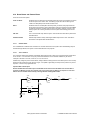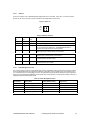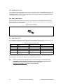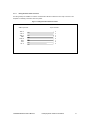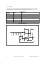
1
L7200SDB
Standard Development System
Hardware User’s Manual
Revision 1.0
Printed on September 2, 1999
LinkUp Systems Corporation
1190 Coleman Avenue, Suite 2C
San Jose, CA 95110
(408) 988-1848
fax (408) 988-3848
www.linkupsys.com
© LinkUp Systems Corporation 1998
Printed in the United States of America
April 12, 1999
All Rights Reserved
This publication is provided “AS IS.” LinkUp Systems Corporation (hereafter “LinkUp”) does not make any warranty of any kind, either
expressed or implied, including, but not limited to, the implied warranties of merchantability and fitness for a particular purpose. Information
in this document is provided solely to enable system and software developers to use LinkUp products. Unless specifically set forth herein,
there are no express or implied patent, copyright, or any other intellectual property rights or licenses granted hereunder to design or
fabricate LinkUp products or products based on the information in this document. LinkUp does not warrant that the contents of this
publication, whether individually or as one or more groups, meets your requirements or that the publication is error-free. This publication
could include technical inaccuracies or typographical errors. Changes may be made to the information herein, and these changes may be
incorporated in new editions of this publication.
The following terms are trademarks of the LinkUp Systems Corporation: LinkUp, L7200.
All other trademarks and registered trademarks are the property of their respective companies.
LinkUp Systems Corporation
1190 Coleman Avenue, Suite 2C
San Jose, CA 95110
(408) 988-1848
(408) 988-3848 fax
www.linkupsys.com
TABLE OF CONTENTS
1.
INTRODUCTION ......................................................................................................................................1
2.
TERMINOLOGY .......................................................................................................................................2
3.
SYSTEM OVERVIEW...............................................................................................................................3
4.
3.1
Packing List....................................................................................................................................4
3.2
Add-on Modules Available from Linkup Systems ...........................................................................5
3.2.1
Add-on Modules Available from Third Parties..................................................................5
3.2.2
System Assembly ............................................................................................................6
3.2.3
Check List Before Board Is Turned On ............................................................................7
L7200SDB MAIN BOARD........................................................................................................................8
4.1
Physical Form Factor .....................................................................................................................8
4.1.1
Main Board Layout...........................................................................................................9
4.1.2
L7200SDB Block Diagram .............................................................................................10
4.2
Memory ........................................................................................................................................11
4.3
Memory Map ...............................................................................................................................11
4.4
GPIO Port Map ...........................................................................................................................12
4.5
Interrupt Assignments ..................................................................................................................13
4.6
Setup Options ..............................................................................................................................14
4.7
J13 and J16 .................................................................................................................................15
4.8
Dynamic RAM ..............................................................................................................................15
4.9
System Flash ...............................................................................................................................15
4.10
Static Memory Expansion Slot .....................................................................................................16
4.11
Boot ROM ....................................................................................................................................16
4.12
ARM Angel Debug Monitor ..........................................................................................................17
4.12.1
Debugger Files ..............................................................................................................17
4.12.2
Installing the Target Specific Files .................................................................................17
4.12.3
Configuring the L7200SDB for Angel.............................................................................17
4.12.4
Downloading and Running Angel from SRAM ...............................................................18
4.12.5
Running Angel from Flash Memory or ROM. .................................................................19
4.12.6
Application Code Location .............................................................................................19
4.12.7
Details of this Angel Port ...............................................................................................19
4.13
LEDs ............................................................................................................................................23
4.14
Reset Button and External Reset.................................................................................................24
4.14.1
Software Reset ..............................................................................................................24
4.14.2
Timers and RTC ............................................................................................................24
4.14.3
Switches ........................................................................................................................25
4.14.4
Power Management Control ..........................................................................................25
4.15
MultiMediaCard Slot.....................................................................................................................26
4.16
Smart Card Interface....................................................................................................................26
4.17
Debug Serial Port.........................................................................................................................26
4.18
Product Serial Ports .....................................................................................................................28
4.19
Logic Analyzer Probes .................................................................................................................29
4.17.1
Debug Serial Port Cable Connection .............................................................................27
L7200SDB Hardware User’s Manual
LinkUp Systems’ Advance Information
iii
4.20
IR Interface ..................................................................................................................................34
4.21
Monochrome LCD and Touch Screen..........................................................................................35
4.22
Monochrome LCD with Touch Screen .........................................................................................35
4.23
4.22.1
VEE Control ...................................................................................................................36
4.22.2
Touch Screen Interface .................................................................................................37
4.22.3
Standard LCD Connector for Color/Mono Panels ..........................................................38
Keyboard......................................................................................................................................40
4.24
PC Card Interface ........................................................................................................................40
4.25
CompactFlash..............................................................................................................................40
4.26
PCI Interface ................................................................................................................................41
4.26.1
General..........................................................................................................................41
4.26.2
I/O Accesses as Initiator ................................................................................................41
4.26.3
Memory Accesses as Initiator ........................................................................................41
4.26.4
Memory Accesses as Target .........................................................................................41
4.26.5
Configuration Space Access as Initiator ........................................................................41
4.26.6
CompactPCI Extensions................................................................................................41
4.26.7
PCI Clock Speed ...........................................................................................................42
4.27
Options.........................................................................................................................................42
4.28
Front Panel ..................................................................................................................................43
4.28.1
4.29
Faceplate Connectors and Labeling ............................................................................................44
4.30
Power Supply...............................................................................................................................45
4.31
Power Measurement ....................................................................................................................46
4.31.1
5.
Markings ........................................................................................................................43
Dynamic Power Measurement.......................................................................................46
BILL OF MATERIALS ............................................................................................................................47
6.
CPU MODULE........................................................................................................................................50
7.
FLASH MEMORY MODULE ..................................................................................................................50
8.
SRAM MODULE.....................................................................................................................................50
9.
CODEC MODULE ..................................................................................................................................50
9.1.1
Voltage Measurement....................................................................................................51
9.1.2
Touch Screen Interface .................................................................................................51
9.1.3
DAA Interface ................................................................................................................51
10. KEYBOARD/LCD MODULE ..................................................................................................................52
10.1
Keyboard Schematic ....................................................................................................................54
11. REFERENCES .......................................................................................................................................55
iv
LinkUp Systems’ Advance Information
L7200SDB Hardware User’s Manual
LIST OF FIGURES
Figure 1. Main Board Assembly ...................................................................................................................... 6
Figure 2. Main Board Layout........................................................................................................................... 9
Figure 3. Block Diagram ............................................................................................................................... 10
Figure 4. J13 and J16 Factory Settings ........................................................................................................ 15
Figure 5. Switch S1....................................................................................................................................... 25
Figure 6. Smart Card Reader........................................................................................................................ 26
Figure 7. Debug Serial Port Cable Connection ............................................................................................ 27
Figure 8. Logic Analyzer Probes ................................................................................................................... 29
Figure 9. SMI Address Signal Assignment.................................................................................................... 30
Figure 10. SMI Data Signal Assignment ....................................................................................................... 31
Figure 11. SDRAM Address/Data Signal Assignment................................................................................... 31
Figure 12. Memory Control Signal Assignment............................................................................................. 32
Figure 13. Serial Ports Signal Assignment.................................................................................................... 33
Figure 14. IR Mini-DIN Plug Pin Position (End View of Receptacle) ............................................................. 34
Figure 15. DC to DC Converter..................................................................................................................... 36
Figure 16. Touch Screen Layout................................................................................................................... 37
Figure 17. LCD Flat Panel Header J15 Footprint .......................................................................................... 38
Figure 18. Faceplate Marking ....................................................................................................................... 43
Figure 19. ATX Power Supply....................................................................................................................... 45
Figure 20. Codec Module.............................................................................................................................. 50
Figure 21. Keyboard/LCD Module................................................................................................................. 52
Figure 22. Keyboard Layout.......................................................................................................................... 53
Figure 23. Keyboard Schematics .................................................................................................................. 54
L7200SDB Hardware User’s Manual
LinkUp Systems’ Advance Information
v
LIST OF TABLES
Table 1. Summary of L7200SDB .................................................................................................................... 3
Table 2. Packing List....................................................................................................................................... 4
Table 3. Documentation and Add-on Modules................................................................................................ 5
Table 4. Third Party Add-on Modules ............................................................................................................. 5
Table 5. Memory Map ................................................................................................................................... 11
Table 6. GPIO Port Assignment.................................................................................................................... 12
Table 7. Interrupt Assignments ..................................................................................................................... 13
Table 8. Setup Options ................................................................................................................................. 14
Table 9. Files Supplied in Angel Debug Monitor Distribution ........................................................................ 17
Table 10. Memory Map After Angel Initialization........................................................................................... 21
Table 11. Data Initialized by Angel................................................................................................................ 21
Table 12. Switch S1 Function ....................................................................................................................... 25
Table 13. Power Management Control ......................................................................................................... 25
Table 14. Debug Serial Port Pin-out ............................................................................................................ 26
Table 15. COM1 Port Pin-out........................................................................................................................ 28
Table 16. COM2 Port Pin-out........................................................................................................................ 28
Table 17. Silkscreen for Logic Analyzer Probes ........................................................................................... 30
Table 18. IR Transceiver Mini-DIN Pin-out ................................................................................................... 34
Table 19. Pin-out Monochrome Panel J31.................................................................................................... 35
Table 20. VEE Control .................................................................................................................................. 36
Table 21. Pin-Out Touch Screen J49............................................................................................................ 37
Table 22. LCD Data Format.......................................................................................................................... 38
Table 23. Pin-out of LCD 40-pin Header J15 ................................................................................................ 39
Table 24. Signal Definitions for LCD 40-pin Header ..................................................................................... 39
Table 25. Faceplate Labeling........................................................................................................................ 44
Table 26. Power Planes................................................................................................................................ 46
Table 27. Bill Of Materials............................................................................................................................. 47
vi
LinkUp Systems’ Advance Information
L7200SDB Hardware User’s Manual
1.
INTRODUCTION
The L7200SDB standard development system is a hardware system used for development with LinkUp’s L7200 Internet
System Processor. Any kind of operating system can be used with the L7200SDB system, however the system is loaded
with a WindowsCE port and driver for L7200 peripherals. It provides an Ethernet connection for fast download of code.
The order number for the L7200SDB system is:
L7200SDB-001
The L7200SDB system consists of the following boards and modules:
•
L7200SDB Main Board, Compact PCI 6U Form Factor
•
L7200 Adapter
•
10/100BaseT Ethernet adapter
•
16 MByte Flash Memory Module with WindowsCE
•
8 MByte Flash Memory Module with Angel debugger
•
Codec Module with UCB1200
•
Keyboard/LCD Monochrome Module 320 × 240 with Touch Screen
•
QWERTY Keyboard
•
Power Supply
This document describes the system's architectural, electrical, and mechanical implementations.
Note:
Please read the Errata Sheet for a list of bugs and workarounds.
L7200SDB Hardware User’s Manual
LinkUp Systems’ Advance Information
1
2.
TERMINOLOGY
NC
The pin is not connected to any signal.
Byte
8 bits of data
Halfword
16 bits of data
Word
32 bits of data
X
Don’t care, the state of this signal does not affect the function in any way.
L
Indicates a low level on a signal
H
Indicates a high level on a signal
RTC
Real Time Clock
CompactFlash (CF) is a registered trademark of the CompactFlash Association, (415) 843-1220, email
[email protected], www.compactflash.org.
2
LinkUp Systems’ Advance Information
L7200SDB Hardware User’s Manual
3.
SYSTEM OVERVIEW
This section is an overview of the L7200SDB system. A brief summary of functions is listed below.
Table 1. Summary of L7200SDB
Item
Comments
Form Factor is Compact PCI
6U 2 Slots wide
System RAM (SDRAM)
32 Mbytes on board, 16 bits wide
System Flash
16 Mbytes, expandable to 16/32/64 Mbytes, 72-pin SIMM module, 32
bits wide
System SRAM
Optional memory up to 8 MByte, 32-bit wide
Boot ROM
512 bytes, on-chip
Software Reset
WDOG output
LED
4 LEDs for status and debug
Debug Serial Port
9-pin Sub D connector
Debug Ethernet Port
N/A
ICE Interface
14-pin header
Timers
See L7200 Databook
PCI Interface
See PCI Interface
Product Serial Port
Serial 1, 2: 9-pin Sub D connector
Keyboard Option 1
Custom scan keyboard, 32 keys - included
Keyboard Option 2
Fujitsu QWERTY keyboard FKB1406
Keyboard Option 3
RS232 to PC Keyboard converter - optional
Logic Analyzer Probes
For Hewlett-Packard logic analyzer
Fast IR, Medium IR, Slow IR
Only slow IR is supported by WinCE
Optional Sharp IR Module
Smart Card Reader
Optional (not supported by WinCE)
MultiMediaCard Interface
8, 16, or 32 Mbyte
LCD and Touch-Screen
on 40-pin connector
PC Card
Type I or II
Compact Flash
Implemented through PC Card slot
L7200SDB Hardware User’s Manual
LinkUp Systems’ Advance Information
3
3.1
Packing List
When unpacking the system, make sure that all of the following items are present. If there is anything missing or other
problems, please contact your sales representative.
Table 2. Packing List
Item #
Qty
Name
Manufacturer
1
1
L7200SDB Main Board
LinkUp
2
1
L7200 Adapter
LinkUp
3
1
Flash Module 16 MByte with WinCE
LinkUp
4
1
Flash Module 8 MByte with Angel
LinkUp
5
1
PC Card to Compact Flash Adapter
6
1
Codec Module with UCB1200
LinkUp
7
1
10/100BaseT Ethernet Module
LinkUp
8
1
Keyboard/Monochrome LCD module
LinkUp
Manufacturer Part #
320 × 240 bits/pixel
9
1
MultiMediaCard Flash, 8 MByte
SanDisk
SDMB-8
Fujitsu
FKB1406
10
1
QWERTY Keyboard
11
2
Null Modem Cable
12
1
ATX Power Supply
Delta
DPS-88AB A (SFX)
(or equivalent)
13
1
Power Cord
14
1
L7200 Internet System Processor
15
1
16
1
LinkUp
L7200-DBK-001
L7200SDB Hardware User's Manual
LinkUp
L7200SDB-HUM-001
L7200 API Reference Manual
LinkUp
Databook
4
LinkUp Systems’ Advance Information
L7200SDB Hardware User’s Manual
3.2
Add-on Modules Available from Linkup Systems
These add-on modules are optional. Some of the modules may be purchased from the original manufacturer.
Table 3. Documentation and Add-on Modules
Item #
Name
Manufacturer
Order #
1
Flash Module 8 Mbyte AMD
LinkUp
L7200SDB-MOD01-001
2
Flash Module 16 Mbyte AMD
LinkUp
L7200SDB-MOD02-001
3
Color LCD Module Dual Scan 640 × 480
Citizen K6488L-FF with backlight
LinkUp
L7200SDB-MOD03-002
4
L7200 Internet System Processor
LinkUp
L7200-DBK-001
Databook
5
L7200SDB Hardware User's Manual
LinkUp
L7200SDB-HUM-001
6
L7200 API Reference Manual
LinkUp
L7200API-REF-001
3.2.1
Add-on Modules Available from Third Parties
These add-on modules are optional and may be purchased from the original manufacturer. Some of these may also be
made available by LinkUp.
Table 4. Third Party Add-on Modules
Item #
Name
Manufacturer
Part #
1
SRAM Module 4 MByte
Cypress
CYM1851V33PM-20C
( also available from Linkup)
2
SRAM Module 8 MByte
Cypress
CYM1861V33PM-20C
3
IR Module
Actisys
IR200L
4
Smart Card Reader
Amphenol
C702 10M008 0152
5
Smart Card
Tritheim
Technologies, Inc.
6
Flash MultiMediaCard, 8 MByte
SanDisk
SDMB-8
7
Keyboard QWERTY
Fujitsu
FKB1406
L7200SDB Hardware User’s Manual
LinkUp Systems’ Advance Information
5
3.2.2
System Assembly
Figure 1. Main Board Assembly
LCD
SRAM
4 Mbyte
(optional)
Keyboard
UCB1200
Module
Flash
16 MByte
Ethernet
Module
L7200 Main
Board
6
LinkUp Systems’ Advance Information
L7200SDB Hardware User’s Manual
3.2.3
Check List Before Board Is Turned On
•
Before unpacking, be sure to be properly grounded and that work surfaces are grounded and static dissipative. Any
electrostatic build-up that is discharged by touching any of the boards may permanently damage the components.
•
Make sure that the ATX power supply is set to the proper line voltage, either 110 or 220V.
The default setting is 110V. Failure to set the correct voltage may permanently damage the power supply and board.
•
Carefully connect the power supply without flexing the board.
•
Check jumper W2, which controls the ATX power supply. This jumper must be closed for the supply to turn on.
•
Check that all components and modules are properly seated.
•
Check that all jumpers are set properly.
L7200SDB Hardware User’s Manual
LinkUp Systems’ Advance Information
7
4.
L7200SDB MAIN BOARD
This section describes the main board of the L7200SDB system. The description starts with a board outline, block
diagram, and L7200-specific control signals, followed by chapters for each interface of the L7200.
4.1
Physical Form Factor
The L7200SDB main board has the physical size of a CompactPCI industry standard for a 6U card (approximately
9 inches × 6 inches). The Compact PCI interface is supported, as outlined in the PCI Interface section.
8
LinkUp Systems’ Advance Information
L7200SDB Hardware User’s Manual
4.1.1
Main Board Layout
Figure 2. Main Board Layout
Bank 1
Flash 32MByte - SIMM72
3 RS232
Bank 2
SRAM 8MByte - SIMM72
IR
IR
L7200
L7200
IO Module
(Optional)
ATX Power
PC Card
(optional)
CPCI-J2
Codec
Module
CPCI-J1
Keyboard Fujitsu
FKB1406 (optional)
L7200SDB Hardware User’s Manual
LinkUp Systems’ Advance Information
9
4.1.2
L7200SDB Block Diagram
Figure 3. Block Diagram
L7200
Compact
PCI
VPC
360 +
Bridge
SDRAM
2 × 16MByte
SDRAM
’244
Header
Power
Management
Flash 16 MByte
SRAM 4 Mbyte (optional)
SMI
Ethernet Module
10/100 BaseT
LCD
Color/Mono
Module
(optional)
CLCD
Mono
MLCD
TL
16C750
LCD
320 × 240
MAX3243
KBD
PC-Card
L1121
MultiMediaCard
Device
Keyboard
Fujitsu
FKB1406
MMC
IR
IR
IRDA
MAX3243
SIB
RS232
UCB1200
Module
UART1
MAX3221
RS232
UART2
SPI
GPIO Module
(optional)
PD
Smart Card
10
LinkUp Systems’ Advance Information
Smart Card
Header
L7200SDB Hardware User’s Manual
4.2
Memory
The following memories are provided on the L7200SDB:
•
512-Byte Boot ROM, on-chip (L7200)
•
5120 Bytes of SRAM, on-chip (L7200)
•
Flash/Static memory slot 1 on 72-pin SIMM module
•
Flash/Static memory slot 2 on 72-pin SIMM module
•
On-board SDRAM, 2 devices, 16 MByte each
•
MultiMediaCard slot
•
Smart Memory Card slot
•
SPI-compatible memory on GPIO module
In addition, memory may reside in the CompactFlash and PC Card slots
4.3
Memory Map
An overview of the memory locations and I/O assignments is shown below. For further details, see the L7200 Data Book.
Table 5. Memory Map
Memory
Space
Address
Function
Boot
ROM
0x0000 0000
0x4000 0000
Boot from on-chip ROM, if bootstrap option PE[0] = 1, in which case the boot ROM is
readable starting at location 0x0000 0000. Whether or not the bootstrap option is
selected, the boot-ROM is always readable starting at location 0x4000 0000.
SRAM
0x6000 0000
On-chip SRAM memory
nIOCS0
0x0000 0000
Flash or SRAM memory
0x2400 0000
Bank 1 is readable starting at location 0x0000 0000 if bootstrap option PE[0] = 0.
Whether or not the bootstrap option is selected, Bank 1 is always readable starting at
location 0x2400 0000.
nIOCS1
0x1000 0000
Flash or SRAM memory
Bank 2
nIOCS2
0x1400 0000
PC Card 1 (on-board)
nIOCS3
0x1800 0000
PC Card/Debug Port
A25 A24
nIOCS4
0x1800 0000
0
0x1900 0000
0
1 Debug UART (TL16C750)
0x1A00 0000
1
0 8-bit Auxiliary Register (write only)
0x1B00 0000
1
1 PC Card 2 (on expansion adapter)
0x1C00 0000
PCI Controller VPC360
L7200SDB Hardware User’s Manual
0
LinkUp Systems’ Advance Information
11
4.4
GPIO Port Map
Table 6. GPIO Port Assignment
GPIO Port
Bit Position
Function
Port A
7:0
Keyboard rows, input to L7200, pulled down with 100 kΩ
Port B
7:0
Data bus D[23:16]
Port C
7:0
Data bus D[31:24]
Port D
7:0
Universal GPIO port on expansion connector
Port E
0
0 - Boot from 32-bit memory in Bank 1 (S1-BT open)
1 - Boot from on-chip ROM (S1-BT closed)
1
0 - Disable VEE for color LCD module
1 - Enable VEE for color LCD module
2
0 - Disable backlight of color LCD module
1 - Enable backlight of color LCD module
3
0 - Disable mono LCD
1 - Enable mono LCD
4
If an external IR module is used, the on-board transceiver has to be turned off.
0 - IR enable (Sharp RY5KD01)
1 - IR disable (Sharp RY5KD01)
5
RI from UCB1200 (active low)
or Status Ready from Flash memory
6
Boot Status from Switch S1-OPT
7
0 - Write enable to Bank 1,2 (S1-WP closed)
1 - Write disable to Bank 1,2 (S1-WP open)
Debug Aux Port
(write only)
0
Unassigned
1
0 - Diagnostic LED on
1 - Diagnostic LED off
2
RTS of Serial Port 1
3
DTR of Serial Port 1
4
Column 12
5
0 - Column 12 Enable
1 - Column 12 Disable
6
Column 13
7
0 - Column 13 Enable
1 - Column 13 Disable
12
LinkUp Systems’ Advance Information
L7200SDB Hardware User’s Manual
4.5
Interrupt Assignments
Table 7. Interrupt Assignments
Interrupt
Function
nEXFIQ
PCI
nINT0
PC Card 1
nINT1
PC Card 2 (Ethernet card)
nINT2
Debug Serial Port
INT3
UCB1200 Interrupt
L7200SDB Hardware User’s Manual
LinkUp Systems’ Advance Information
13
4.6
Setup Options
Following is a list of jumpers that select board options. The default settings are shown in bold.
Table 8. Setup Options
Jumper
Sheet
Position
Default
J28
3
1+2
Closed
Not applicable
J45
4
1+2
Open
Stand-alone operation with ATX power supply
J1
5
1+2
Open
Closed
J2
5
1+2
Description
Comment
System wakeup
Required after hardware
Power on Reset
Open
Closed
Power-on reset
J3
1
See Power Management Control
J13
6
See J13 and J16
J16
6
See J13 and J16
J28
3
1+2
J39
5
1+2
VDDIN power measurement
Voltage across 1 Ω resistor
J40
5
1+2
VDDR power measurement
Voltage across 0.1 Ω
resistor
J41
5
1+2
VDDRC power measurement
Voltage across 0.1 Ω
resistor
J42
5
1+2
VDDA power measurement
Voltage across 1 Ω resistor
J38
5
1+2
VDDM power measurement
Voltage across 0.1 Ω
resistor
J37
5
1+2
Open
Closed
Disable 18.432 MHz oscillator
J35
5
1+2
Open
Enable 48 MHz oscillator
Closed
Disable 48 MHz oscillator
J33
J36
W4
14
5
5
5
1+2
Open
PCI Frequency 16MHz
Enable 18.432 MHz oscillator
Open
Isolate 9.216 MHz oscillator from L7200
Closed
Connect 9.216 MHz oscillator to L7200
Open
Enable 9.216 MHz oscillator
Closed
Disable 9.216 MHz oscillator
1+2
open
PE[5] connect to RI of Codec
2+3
open
PE[5] connect to Flash Status bit
1+2
LinkUp Systems’ Advance Information
L7200SDB Hardware User’s Manual
4.7
J13 and J16
J13 and J16 form a jumper block of 3 rows by 8 positions. The upper rows are connected to port PE[0] through PE[7],
which are inputs sampled by the L7200 on the rising edge of the power-on reset signal nSTPOR. Care must be taken that
the strapping options selected by PE[0] through PE[4] are set properly. Failure to do so may result in unpredictable
behavior. PE[5] through PE[7] are assigned to control functions as described above.
Figure 4. J13 and J16 Factory Settings
PE
J13
J16
0
1
2
3
4
5
6
7
Signal
High
Low
PE[0]
BOOTEN: The state of this signal is determined by switch S1-BE and may be high or low. If PE[0] is high (S1BE closed), then the L7200 will boot from the on-chip ROM. See also S1 for a detailed description.
PE[1]
PLLBYPASS: This signal should be high only when an external CPU clock is desired. Usually this signal is low.
ENAVEE: During normal operation, PE[1] enables VEE for the LCD mono or color panel
PE[2]
E18M: If this signal is high while PE[1] is high, it indicates to the L7200 that an 18.4 MHz oscillator in Y5 is
connected to STCLK, otherwise a 13 MHz clock is assumed. PE[2] is ignored if PE[1] is low.
ENABKL: During normal operation, PE[2] will control the backlight of the mono or color LCD.
PE[3]
IO16BIT: When low, the L7200 handles Bank 0 (nIOCS0) as 32-bit memory. The L7200SDB board supports
only 32-bit wide memory in Bank 0. All other banks have to be set for 32-bit access under software control.
LCDON: During normal operation, PE[3] controls the monochrome panel.
PE[4]
PCCARD: This signal must be high at power-on reset. The L1121 (U7) is used to translate the upper address
bits of the static memory controller into a 26-bit wide address.
NIREN: During normal operation, PE[4] controls the Sharp IR module.
PE[5]
RI or Flash Status: PE [5] is pulled low by the default setting, because W4 has no signal connected.
PE[6]
PE[6] is used as a status bit selectable by S1. For a description, refer to the S1 description.
PE[7]
Write Protect: PE[7] must be pulled low. If S1 WP is jumpered, then writes to Bank 1 or 2 of the static memory
are enabled (default setting). PE[7] may be controlled by software to protect memory from being overwritten.
4.8
Dynamic RAM
The L7200SDB provides for 32 Mbytes of SDRAM soldered to the board, with no provision for DRAM expansion. The
system RAM can be expanded by placing SRAM in the static memory expansion slot.
4.9
System Flash
The L7200SDB provides 16 MBytes of linear Flash memory on a custom 72-pin SIMM module. Static memory can also be
expanded by installing an SRAM 72-pin SIMM module in that slot.
The L7200 is able to block erase and block protect the Flash memory with a granularity of 512 KByte/block. The L7200 is
able to write to Flash memory in words or bytes. There is a software-controlled, global write-protect register bit
implemented through GPIO port PE[7]. This bit prevents the hardware from asserting the write-enable signal, which
disables all writes to Flash memory.
L7200SDB Hardware User’s Manual
LinkUp Systems’ Advance Information
15
Bank 1 of the static memory interface of the L7200 (nCS0) is intended for Flash memory, but may be used for SRAM.
Using the in-circuit emulation tools for download SRAM may be preferred in some environments. The static memory
controller is configured for 32-bit wide memory in Bank 1 at boot time.
The memory is configured for word and byte operation. A few gates of glue-logic are necessary to enable byte write and
write deselects. Writes to memory may be deselected under software control by setting port PE[7] = 1 or by setting Switch
S1.3 to the off position. In the latter case, software cannot override the write disable.
4.10
Static Memory Expansion Slot
The L7200SDB provides a static memory expansion slot for a 72-pin SIMM. A 4-MByte SRAM module is bundled with the
system, but this slot may also be occupied by Flash memory.
4.11 Boot ROM
During normal operation, code executes from the system Flash memory. However, when the system Flash memory is
blank or has become corrupt, a mechanism is provided to reprogram the system Flash. By selecting options on switch S1
(see Section 4.14.3), the system can be made to boot from the serial port 1 (Com 1) or the MultiMediaCard slot. This is a
feature provided by the L7200 embedded boot ROM (see Reference [1] for more details).
The supplied MultiMediaCard device contains monitor code for the ARM debug monitor, called Angel. The debug monitor
communicates using the Angel Debug Protocol (ADP) to the ARM symbolic debugger running on a host PC. Angel
transfers data through the serial debug port at a rate of 38.4 kbaud (8 data bits, 1 stop bit, no parity).
Once the system is taken out of reset and the switch settings indicate the use of the boot ROM, the L7200SDB board
identifies itself over the debug serial port. The ARM debugger (ARMSD) on the host PC interprets the communication
protocol and provides a debugging environment.
16
LinkUp Systems’ Advance Information
L7200SDB Hardware User’s Manual
4.12 ARM Angel Debug Monitor
This describes the port of the Angel Debug Monitor to the LinkUp Systems L7200SDB Standard Development System.
This port may require changes to work on any other L7200 system. For generic Angel information refer to the user
documentation supplied with the ARM SDT2.50 (Software Development Toolkit).
4.12.1
Debugger Files
Only the target-specific files are included in this release. Merging these with the generic Angel sources is described in the
next section.
Table 9. Files Supplied in Angel Debug Monitor Distribution
File Name
Comments
ReadMe.txt
l7200eval\banner.h
l7200eval\devconf.h
l7200eval\devices.c
l7200eval\linkup.h
Configuration options
l7200eval\mmu.s
Macros for controlling the MMU
l7200eval\platform.h
l7200eval\SDRAM.s
SDRAM autosizing macros
l7200eval\stacks.c
Replacement for generic Angel version
l7200eval\stacks.h
Replacement for generic Angel version
l7200eval\target.s
l7200eval\tl16c750.c
l7200eval\tl16c750.h
l7200eval\makelo.c
l7200eval.b\APM\AngL7200.apj
The SDT2.50 project (build) file
l7200eval.b\APM\Image\AngL7200.elf
l7200eval.b\APM\Image\AngL7200.rom
Prebuilt L7200 Angel ROM image
l7200eval.b\APM\Image\AngL7200.sym
Prebuilt ADW symbol table for above ROM image
4.12.2
Installing the Target Specific Files
The target-specific source files are found in the l7200eval\ directory. The l7200eval.b\ directory contains a project
file for the ARM SDT2.50 and ready-built images of Angel. Both directories should be placed in the Angel source tree, in
the directory Arm250\Angel\Source. The images can then be rebuilt using the APM project file. The files stacks.c
and stacks.h in the l7200eval\ directory are used in preference to those in the standard Angel source.
If you make a copy of the Angel directory elsewhere in your directory structure (other than in the Arm250 directory) then
Angel will fail to build as it requires a file objmacs.s from the Arm250\cl\ directory. This can be fixed by copying this
file into the new Source\ directory of the copied Angel.
4.12.3
Configuring the L7200SDB for Angel
4.12.3.1 Memory Cards
The L7200SDB has two slots for static memory cards, Slot 1 (appears as the CS0 memory bank) and Slot 2 (CS1
memory bank). Either slot can take an SRAM card, a Flash memory card, or a ROM card. This port of Angel assumes that
the Angel ROM image is held in a block of memory which appears at address 0x0 at reset. For the L7200 evaluation
board this must be a card in Static Memory Slot 1 on the board. Therefore, Slot 1 must be populated with the memory
card containing (or to contain) the Angel Debug Monitor.
L7200SDB Hardware User’s Manual
LinkUp Systems’ Advance Information
17
If an SRAM card is used, then the Angel image must be downloaded using an ARM MultiICE after power-up. If Flash or
ROM cards are used, then these must be programmed with the Angel ROM image before being used.
4.12.3.2 Boot Options
When using Angel, make sure the jumper BT on the front panel of the board is unconnected. There are two hardware
selectable memory maps. If the jumper BT on the front panel is connected, then the on-chip PROM is aliased to zero at
reset and the expansion memory at slot 1 is mapped to 0x24000000. If the jumper is not connected, then the on-chip
PROM is not aliased and the memory slot 1 is mapped to zero. If the first option is selected then the second (required)
map is reached by writing to the remap register. The ADM software assumes that it starts running in slot 1 memory at
address zero, i.e. the default memory map.
4.12.3.3 Serial Connection
Angel communicates with the L7200 evaluation board via a serial connection. Connect the host computer to the board
with a serial cable attached to the Debug Serial Connector via the adapter supplied with the board.
4.12.3.4 Memory Management Unit
The L7200 has an ARM720T as the CPU. This processor has an MMU (Memory Management Unit) and a unified
instruction and data cache with write buffer to improve performance when the CPU is clocked faster than the memory.
The MMU uses page tables to mark which areas of memory can be cached or write buffered. These page tables can also
be used to map any virtual address (the addresses the CPU core sees) to any physical address (the addresses which are
passed to the physical memory bus). This is done in blocks. A level 1 page table describes memory in 1-Mbyte blocks. If
finer control is required, a level 2 page table could be used to describe 4-Kbyte blocks.
The L7200SDB has one or two banks of SDRAM as the primary RAM used by the ARM CPU. Three DMA controllers can
also access the SDRAM, a peripheral DMA block (which reads and writes to SDRAM), and a pair of LCD controllers
(which read only). These DMA controllers access the SDRAM directly, and therefore the addresses they use are not
remapped by the L7200 MMU. Because the DMA controllers are on the other side of the cache from the CPU, if an area
of memory marked as cacheable is written by DMA, then the CPU may not see the change. This can be prevented by
marking areas used by DMA as uncacheable.
The spaces provided for the SDRAM banks are both 16 Mbytes in size. Bank 1 always starts at address 0xF0000000 and
may be populated with 2, 8, or 16 Mbytes. Bank 2 always starts at address 0xF1000000 and may be populated with 0, 2,
8, or the full 16 Mbytes.
If a bank is only partially populated, then that memory appears aliased (mirrored) multiple times to fill the whole bank. For
example, if bank 1 contains 8 Mbytes and bank 2 has 16 Mbytes, the memory map would be:
0xF1000000 to 0xF1FFFFFF 16 Mbytes in bank 2
0xF0800000 to 0xF0FFFFFF alias of the 8 Mbytes in bank 1
0xF0000000 to 0xF07FFFFF 8 Mbytes in bank 1
There will always be a contiguous block of memory around the address between the two banks (0xF1000000), starting at
address (0xF1000000 - size of bank 1) and ending with address (0xF1000000 + size of bank 2). This aliasing is a feature
of the SDRAM system, not the L7200 processor.
4.12.4
Downloading and Running Angel from SRAM
The file AngL7200.rom in the l7200eval.b\APM\image\ directory is the prebuilt downloadable ROM image of Angel
(this will be overwritten if you rebuild the project). This file should be downloaded to address 0 (with SRAM in slot 1).
Ensure MultiICE is connected to the board and the MultiICE server is running correctly. Run the ADW (ARM Debugger for
Windows from the SDT2.50 toolkit). Select the File->Get File menu option. Set the filename to the path of the
AngL7200.rom file, and set the address to download the file to 0 (the default of 0x8000 will not work). This downloads
the file to the board. Because this is a bare ROM image (rather than a standard application image) you will have to set up
the debugger to run this image correctly:
1.
Select menu option View->Debugger Internals. The Debugger Internals window appears.
2.
Clear the value of vector_catch in the Debugger Internals window to 0 (all the letters will appear lower case). This
prevents the debugger trying to catch the processor vectors which Angel will need to use in real time.
3.
Clear the value of semihosting_enabled to 0. This prevents the debugger from processing Angel’s SWI calls.
4.
Select menu option View->Registers->Current Mode. The Registers window will be displayed.
18
LinkUp Systems’ Advance Information
L7200SDB Hardware User’s Manual
5.
In the Registers window, set the value of register pc to address 0. The Angel ROM image needs to run from 0 to
correctly initialize. Setting the program counter also is the only way that the debugger will allow the code to be run.
6.
You should now click the Go button. This operation also has a menu equivalent, under Execute->Go.
The Angel debug monitor should now be running. Do not stop the execution in this invocation of the debugger or else
Angel will be halted.
You can now start a second debugger session to talk to Angel directly. Remember that when the debugger starts it will
ask "Are you sure you want to start in remote debugging?". Do not connect to hardware at this stage (as a second
connection will be attempted to MultiICE, which is bad). Instead, click "No". An ARMulator (simulated) connection will be
started. Go to the menu option Options->Configure Debugger and set the debugger up as described in the next section.
4.12.5
Running Angel from Flash Memory or ROM.
This section assumes that the Angel ROM image is already programmed into the card in slot 1.
1.
Run the ADW debugger. If it asks "Are you sure you want to start in remote debugging?" then click "No" for the first
time you run Angel. Go to the menu option Options->Configure Debugger which brings up the Debugger
Configuration window. In this window select remote_a as the target environment (which is the Angel protocol).
2.
Click "Configure" to bring up the Angel Remote Configuration window. From this window, select which serial port is
used on the host PC. Ensure that the Heartbeat option is selected (ticked).
3.
Configure the baud rate as high as possible (115200 baud is recommended).
4.
Select "OK" from both the Angel Remote Configuration window and the Debugger Configuration window. The
debugger will start to access the L7200SDB through Angel. After a few seconds, the Angel start-up banner should be
displayed in the Debugger Console window. If it does not, then check the serial connection and configuration options.
Applications can now be downloaded and run using Angel. See the generic Angel documentation supplied with SDT2.50
for more details.
4.12.6
Application Code Location
Downloading applications to the default location of 0x8000 will work, provided they fit in the available SDRAM. If
downloading to other locations, ensure that the image does not overlap any areas of memory used by Angel. Angel uses
the workspace from the vectors upwards, so assume that the address range 0x0 to 0x8000 is in use. It will usually only
use a small part of this range, but the size will grow if various Angel compile time options are enabled.
The very top of the SDRAM will be used for both the Angel and application stacks, as well as the MMU page table. The
on-chip SRAM is not used by Angel. Static memory in Slot 1 is only used to hold the Angel image, so any remaining
memory can be used for other purposes. Static memory in Slot 2 is not used by Angel.
4.12.7
Details of this Angel Port
This section describes details which are specific to Angel for the L7200SDB.
4.12.7.1 Start Up Code
At initialization the clocks are set, the SDRAM is configured, the memory manager started with a single level 1 page table
(see sections below). No other configuration or initialization is carried out. In particular, the SRAM or Flash and the GPIO
are not configured.
4.12.7.2 Clock Settings
Clock settings are:
CPU
64.512 MHz
SDRAM FCLCK
64.512 MHz
SDRAM BCLCK
32.256 MHz
BCLCK
32.256 MHz
L7200SDB Hardware User’s Manual
LinkUp Systems’ Advance Information
19
All the peripheral sub-system clock settings are not explicitly set. If an application is going to use a peripheral block, it
should ensure that that it is correctly clocked.
4.12.7.3 SDRAM Configuration
The SDRAM width (8-bits or 16-bits wide) and the number of banks within each SDRAM device (2 or 4 banks) is
configured at Angel compile time by the settings of SDRAM_CONFIGURATION in the linkup.h file. The pre-built Angel
supplied assumes 2 banks of 16-bit wide (or 64 Mbit × 8) SDRAM. It should still work if only the lower bank is filled,
although unnecessary power consumption may result from running a non-existent bank. Each SDRAM device is assumed
to have 4 internal banks.
By default the other options are set as shown below:
•
CAS latency is set to 2.
•
Refresh is enabled.
•
Auto-precharge is enabled for DMA ASB, Main ASB, and LCD accesses.
•
Both SDRAM write buffers are enabled.
•
The CKE clock enables are asserted to all devices all of the time.
•
The bus tri-state controller re-drives the last data onto the SDRAM bus after every access.
4.12.7.4 Memory Management
The customized Angel initialization sequence for the L7200SDB involves mapping the memory using the L7200's Memory
Management Unit (MMU). This is required for the following reasons:
•
The SDRAM must be mapped to 0 to allow the exception vector address table to be in RAM. This allows user
exception handlers to be patched in.
•
The SDRAM is in one or two banks each with a maximum size of 16 Mbytes. If bank 1 is not fully populated, then
there will either appear a gap between the banks, or the start of bank 1 will have to be higher. Memory mapping
ensures that the whole available SDRAM is mapped contiguously at a known location (address 0x0000 0000).
•
Areas of memory can only be marked as cacheable and write-bufferable using the MMU.
•
The memory mapping is performed using a page table. Its physical location may vary depending on the size and
number of SDRAM banks. It maps an aliased copy of itself to a fixed virtual address so that user code can access it.
The following memory management is performed by the custom initialization:
•
The number of SDRAM banks is ascertained, and then each bank is autosized. This is done by writing and reading
from locations in each bank (the original data values are restored). Only sizes of 2, 8, and 16 Mbytes are supported
in each bank in the autosizing routine (i.e. only 16-, 64-, and 128-Mbit devices are detected).
•
A level 1 page table is created at the top of the second physical SDRAM bank (address 0xF2000000 - 16 Kbyte =
0xF1FFC000, where 16 Kbyte is the size of the page table).
•
If there is no bank 2, then the page table is placed at the top of bank 1.
•
Only a level 1 page table is implemented here, which has a granularity of 1 Mbyte. This page table will take up the
top 16 Kbytes of the physical (and virtual) SDRAM.
•
Page tables are set to map the whole 4 Gbyte memory space on a one to one basis (i.e. all virtual addresses will
now map to the corresponding physical address) before the individual areas are remapped. The whole of the
memory space is marked as uncacheable and non-write bufferable.
•
An alias of the page containing the page tables is created at a fixed address (0xF2000000 - 16 Kbyte =
0xF1FFC000). Since the granularity of the level 1 page table used is 1 Mbyte, this requires the page starting at
0xF1F0000 to be mapped. In some situations, this page may be mapped to where it already existed physically. The
label VirtualPageTableBase is set to point to this fixed location for easy access.
•
The highest aliased version of SDRAM bank 1 (address 0xF1000000 - size of bank 1) is mapped using the MMU to
two virtual locations. The copy at virtual address 0x00000000 is marked as cacheable and write bufferable. The copy
at virtual address 0xF0000000 is marked as uncacheable and non-write bufferable.
•
The lowest aliased version of SDRAM bank 2 (address 0xF1000000) is mapped using the MMU to two virtual
locations, above the virtual copies of bank 1, to form contiguous blocks. The copy at virtual address (0x00000000 +
size of bank 1) is marked as cacheable and write bufferable. The copy at virtual address (0xF0000000 + size of bank
1) is marked as uncacheable and non-write bufferable.
•
The static memory banks (CS0 and CS1) and the on-chip SRAM are marked as cacheable and write bufferable. This
may cause problems if one of these banks contains Flash memory. Do not write Flash memory in an area that is
cached. You should either disable caching for this area temporarily during the write operation (and then flush the
caches) or disable caching permanently for this area.
20
LinkUp Systems’ Advance Information
L7200SDB Hardware User’s Manual
The default final virtual memory map after Angel initialization is shown in Table 10.
Table 10. Memory Map After Angel Initialization
Address
Description
0xF0000000
Virtual copy of SDRAM, contiguous block (uncacheable). This is a virtual copy of the block
of memory from the physical address (bank 1 base + 16 Mbytes - size of bank 1) onwards.
0x60000000
On-chip SRAM (cacheable and bufferable)
0x24000000
CS0 (Static Memory Bank 1) (cacheable and bufferable)
0x10000000
CS1 (Static Memory Bank 2) (cacheable and bufferable)
0x00000000
Virtual copy of SDRAM, contiguous block (cacheable and bufferable). This is a virtual copy
of the block of memory from the physical address (bank 1 base + 16 Mbyte - size of bank 1)
onwards.
Initialization also creates the data structures shown in Table 11.
Table 11. Data Initialized by Angel
Address
Description
0xF1FFC000
Virtual alias of the page table. Always access the page table using this address because it
is uncached and at a fixed location. Don’t use this address if the MMU is turned off.
0xF1FFBFFC
Stored value of the size of bank 2 of SDRAM in Mbytes.
0xF1FFBFF8
Size of bank 1 of SDRAM in Mbytes.
0xF1FFBFF4
Pointer to the physical address of the page table. If you copy this pointer elsewhere, then
you can use it to access the physical page table if the MMU is turned off.
0xF1FFBFF0
Pointer to the physical address of the base of the contiguous block of SDRAM (bank 1 base
+ 16 Mbytes - size of bank 1).
4.12.7.5 Autosizing
As shown in the above memory map, the results of the Angel SDRAM autosizing exercise during initialization are stored
at virtual addresses 0xF1FFBFF8 and 0xF1FFBFFC. The possible values of each of these are 0, 2, 8, and 16, although
Angel will fail if bank 1 has a value of 0.
4.12.7.6 DMA Issues
The SDRAM is shared between the CPU and the various DMA controllers (i.e. the peripheral DMA controller and the two
LCD DMA controllers). For best performance, the CPU uses the cached alias of the SDRAM from address 0x00000000
upwards.
The DMA controllers need to be given the offset of the physical address to access from the start of the SDRAM base
address (0xF0000000), this offset can be between in the range 0 to 32 Mbytes. The DMA controllers access the SDRAM
directly, and do not use the virtual to physical mapping provided by the MMU.
Care must be taken to avoid the following problems:
•
The CPU should not cache or write buffer memory locations used for DMA buffers. Otherwise, the CPU may not see
the DMA update the buffers, and the DMA may not see the CPU update the buffers. This can be avoided by using
the uncached image of the SDRAM starting at virtual address 0xF0000000, rather than the cached version at virtual
address 0x0000000.
•
If there is less than 16 Mbytes of memory in SDRAM bank 1, then there will be a discontinuity between the two
SDRAM banks, and a DMA buffer which overlaps the two physical areas might fail. This only happens if the lowest
alias of the SDRAM bank 1 in the 0xF0000000 to 0xF0FFFFFF range is used as the DMA start address. If the start
of the DMA buffer uses the highest alias of the SDRAM bank 1 in the 0xF0000000 to 0xF0FFFFFF range, then any
DMA access which overruns the end of bank 1 will run straight into the SDRAM bank 2, which avoids the problem.
There are two ways an application can manage DMA buffers:
•
A fixed area of memory is set aside for DMA buffers.
•
DMA buffers are dynamically allocated at run time using a C function like malloc().
Great care must be taken in both cases.
L7200SDB Hardware User’s Manual
LinkUp Systems’ Advance Information
21
In the first case, one possible place to put the DMA buffers would be between the page tables at the top of memory and
the stacks. This would require altering the value of compile variable Angel_StackBaseOffsetFromTopMemory in the
file dev_conf.h to lower the stacks by the required amount.
In the second case the sequence of events should be the following:
1.
Allocate a DMA buffer using malloc() or some other method. This will return an address pointer in the range
0x00000000 to 0x02000000, which is in the cached virtual copy of the SDRAM. This should also ensure that the
application does not accidentally use this area for any other purpose.
2.
To get a pointer to the uncached virtual copy of the SDRAM add on the offset 0xF0000000 to the original pointer. All
accesses to the buffered area should now use this pointer.
3.
You must now flush the MMU write buffers. Otherwise if they contain an outstanding write to this buffer, it may
overwrite the DMA buffer some time later.
4.
The offset to pass to the DMA block should be calculated by taking the original pointer, and adding on 0x01000000
(16 Mbytes) and subtracting the size of bank 1 of SDRAM.
5.
After all the DMA transfers have occurred, you can go back to using the cached version of the buffer if you flush the
caches. If you are just going to reuse the buffers, but not the data, then this is not required.
The above method has the advantage that the cache does not need to be flushed each time the buffer is accessed. If a lot
of CPU processing is to take place on the DMA buffer in place, then it may be more efficient to use an alternative
approach in which the cached version of the buffer is used, and the caches are flushed before or after each DMA transfer
has completed.
If the on-chip SRAM is being used as an LCD frame buffer, then its entry in the page tables must be changed to make it
uncacheable and non-write-bufferable.
4.12.7.7 Piccolo Issues
Piccolo directly accesses the main system bus to read its instruction stream, bypassing the MMU. The base address of its
instruction stream (the address of the next function to execute) is passed to it by the ARM using a PSTART instruction.
However, the ARM will be running under virtual memory. The user must convert the virtual function address seen by the
ARM to the actual physical location of the function before passing it to the Piccolo. This only affects addresses used by
the PSTART instruction, as all the data is passed via the ARM using virtual addresses to the data is correct.
4.12.7.8 Stack Location and Size.
The Angel and application stacks are currently at the top of the SDRAM (but below the page table, and 8 words of
memory used to store the results of the SDRAM autosizing). The default application SVC stack size is set in the generic
Angel file Stacks.h by the definition of Angel_ApplSVCStackSize. The default is only 0x80 bytes. To increase the
default stack size, modify this definition and recompile Angel. Alternatively, Angel allows for the user application to move
the application stack to a separate location (simply overwrite the stack pointer).
4.12.7.9 Page Table
There is a single level 1 page table. This is located at the top of SDRAM. The four main chunks of memory (Slot 1, Slot 2,
on-chip SRAM, and the virtual copy of SDRAM at address 0x0) are marked as cacheable and write bufferable. No other
memory is so marked. All sections of memory are in domain zero with user read/write access.
The only sections of memory that will produce an access fault are the portion of the 64 Mbytes of address space with
base zero that does not correspond to the SDRAM mapped to zero. To access the page table use
VirtualPageTableBase, which points to the first entry after any remapping has been carried out.
4.12.7.10 Changes Required in Platform-independent Code
In the debug version we have set DEBUG_BASE to point into the remapped slot 1 memory. This address is out of range for
the MOV command on line 463 of startrom.s and so has to be replaced by the line shown below.
LDR
r1, =DEBUG_BASE
This change affects a debug version of Angel only.
4.12.7.11 Debug Version
This uses logterm debugging through the on-chip UART 2: 115200 bps, 8 data bits, 1 stop bit, 1 start bit.
22
LinkUp Systems’ Advance Information
L7200SDB Hardware User’s Manual
4.12.7.12 Building Angel
The SDT2.50 project (build) file AngL7200.apj in the directory l7200eval.b\APM\ is used to rebuild the Angel project.
The build process will produce 45 warnings. These have been introduced due to a higher level of warning notification
being enabled than used previously, the warnings should be removed for future releases of Angel.
This produces the AngL7200.rom, AngL7200.sym, and the AngL7200.elf images in the
l7200eval.b\APM\Images\ directory.
The AngL7200.rom image is the image to download to the board. The AngL7200.sym file is a symbol table which can
be loaded by the Debugger and used to help debugging Angel via MultiICE. After downloading the ROM image the
symbol table can be loaded by choosing the menu option File->Load symbols only. This brings up the Open dialog box,
which is used to select the symbol file. The Files of Type box in the Open dialog box will have to be set to All Files (*.*) to
see the symbol file. The symbols refer to locations after Angel’s remapping of the memory during initialization, so do not
rely on these symbols until the MMU has been enabled.
4.13 LEDs
There are 4 LEDs visible from the faceplate. Their functions are described below.
Red LED
The red LED is on when the L7200 is in Run mode.
Green LED
After power-on, the green LED is turned on by reset. Typically, as soon as the CPU comes out of
reset the LED is turned off by software, indicating successful boot-up. When the operating system is
running, the kernel periodically may toggle the LED, indicating normal operation.
The green LED is on during reset and remains on until software turns it off by writing to the BUZ
control bit. This LED is under software control during normal operation and may be used for debug
purposes.
Yellow LED
The yellow LED is controlled by the Watchdog output. It is turned on when the Watchdog Timer
expires.
Amber LED
The amber LED is driven by the Auxiliary Port bit 1 and is not affected by power-on reset or by user
reset. After power-up, this LED is on.
L7200SDB Hardware User’s Manual
LinkUp Systems’ Advance Information
23
4.14 Reset Button and External Reset
There are several reset options.
Power On Reset
Hardware Power on Reset from the faceplate. When this jumper is momentarily connected,
the whole system and L7200 is reset. The wakeup jumper has to be shorted to get the
L7200 out of Deep Sleep mode and into the Run mode.
Reset
Hardware reset from the faceplate. When temporarily connected, this jumper resets the
whole system and gives the L7200 a partial reset in which the real-time clock and SDRAM
contents are preserved. A partial reset may also be invoked by software. A pulse on the
wakeup input to the L7200 is generated, so that the system automatically goes into Run
mode.
ICE reset
The in-circuit emulator may reset the system. This has the same effect as the partial reset
described above.
Software Initiated
Software may initiate a reset by asserting the WDOG output of the L7200. This has the
same effect as the partial reset described above.
4.14.1
Software Reset
The L7200SDB has a software reset mechanism for cold reset and reboot of the system. When the Watchdog output is
asserted through software, the system is reset. Header W2 has to be jumpered.
4.14.2
Timers and RTC
The L7200 has various timers capable of periodically interrupting the CPU. These may be programmed for periods from 1
ms to 100 ms in 1 ms increments. A very low power timer derived from the 32.768 kHz oscillator may be used for
interrupts in intervals of 31.25 ms, 15.62 ms, 7.81 ms, and 3.91 ms.
Software may change the period of these timers, setting a different interrupt period for each interrupt event. The accuracy
depends on the 32.768 kHz crystal, which is 20 ppm. It is capable of generating an interrupt to the processor any time of
day within 1 second of its programmed time.
Important Note: 32 kHz option
Rev AA and Rev AB of the L7200 require a 32.000 kHz source that is fed into the IRCLK if an accurate RTC is
required. The IRCLK is serving as a real-time clock source if the input pin nINT2 is low at power on reset. This
feature has to be enabled on the board by removing R88 and installing R89 and R32.
U36A
U36B
R32
1
2
3
4
30kHz
IRCLK
IRCLK
5
33
74AC04
74AC04
R86
200k
R87
10M
Y7
32.000kHz
C130
27pF
GND
24
C129
27pF
GND
LinkUp Systems’ Advance Information
L7200SDB Hardware User’s Manual
4.14.3
Switches
There are 3 switches in the L7200SDB faceplate implemented as a 2-row header. In this case, ’on’ means a jumper is
present and ’off’ when no jumper is present. All switches are independent from each other.
Figure 5. Switch S1
BT
OPT
WP
Table 12. Switch S1 Function
Switch
1.1
Switch
1.2
Switch
1.3
Function
PE[0]
PE[6]
PE[7]
Port E assignment
BT
OPT
WP
Faceplate naming
ON
X
X
Code executes from the boot ROM following reset and communication
is over Asynchronous Serial port 1. If a MultiMediaCard device is
inserted, the system boots from the card instead.
OFF
ON
X
Code starts executing from system Flash memory after reset. The
debug serial port is used for debug communication.
OFF
OFF
X
Code starts executing from system Flash memory after reset. The
Ethernet port is used for debug communication.
X
X
ON
The block write protection for the system Flash memory is enabled.
Protected blocks cannot be written.
X
X
OFF
The block write protection for the system Flash memory is disabled.
Protected blocks can be written.
4.14.4
Power Management Control
The L7200 provides a number of control signals that are used to signal battery status, power failure, and other conditions.
These Power Management Control signals are buffered by a 74AC244. The input voltage swing may be between 0 and
3.3V. All signals go to the corresponding pins of the L7200. Because all input signals are pulled up and some signals are
active high, such as BATOK and MEDCHG, these signals have to be jumpered by connecting them to GND or driven by a
signal that selects the desired system mode.
Table 13. Power Management Control
Front Panel
Description
Jumper Default Setting
Active Level
BATOK
Battery OK signal
closed
high
MEDCHG
Media Change signal
closed
high
nPWRFL
Power Fail signal
open
low
nEXTPWR
External Power signal
open
low
nBATCHG
Battery Change signal
open
low
L7200SDB Hardware User’s Manual
LinkUp Systems’ Advance Information
25
4.15 MultiMediaCard Slot
The L7200SDB provides a MultiMediaCard slot. This may be used for either Flash or ROM MultiMediaCard devices. The
card may also be used to load programs and data into the on-board Flash memory. The L7200 can be bootstrapped from
a MultiMediaCard device, which is much faster than loading memory through the serial port. The MultiMediaCard device
can be programmed with a PC Card adapter.
4.16 Smart Card Interface
The L7200 provides a direct interface to a Smart Card. If a card is inserted, the board applies power through a power
MOSFET TR3. Only 5V cards are supported. The card reader is a Push-Push type from Amphenol. For a description of
the card interface see the L7200 Databook.
Figure 6. Smart Card Reader
4.17 Debug Serial Port
The L7200SDB has a debug serial port with a default baud rate of 38.4 kbaud. This port uses a male DB9 connector with
a pin-out identical to a standard PC. Connect the host PC to the board with a null modem cable.
Table 14. Debug Serial Port Pin-out
Pin
Name
Pin
6
DBG_DSR
2
DBG_RX
7
DBG_RTS
3
DBG_TX
8
DBG_CTS
4
DBG_DTR
9
V12V+
5
GND
1
Name
The debug serial port (DBG_RX, DBG_TX) supports a serial data format of 8 data bits, 1 stop bit, and no parity. The
debug serial port is used exclusively for debug and is not shared with any other function.
Note:
26
V12V+ on pin 9 may be protected by fuse F1, however this fuse is not installed in the
L7200SDB as shipped. If V12V+ is required to connect a standard PC keyboard with an
interface adapter such as the AT-2-Serial from Access Keyboards
http://www.accesskb.demon.co.uk, then F1 must be installed.
LinkUp Systems’ Advance Information
L7200SDB Hardware User’s Manual
4.17.1
Debug Serial Port Cable Connection
The debug serial port is available on J9 and is connected with a flat ribbon cable to the sub-D 9-pin connector on the
faceplate. The following connections have to be present.
Figure 7. Debug Serial Port Cable Connection
SUB-D 9-pin male
10-pin connector
-RxD 2
-TxD 3
-DTR 4
GND
-DSR 6
-RTS
-CTS
2
3
4
5
6
7
8
12V 9
9
L7200SDB Hardware User’s Manual
LinkUp Systems’ Advance Information
27
4.18 Product Serial Ports
The L7200SDB has two product serial ports. UART1 on the L7200 is connected to COM1, and UART2 is connected to
COM2 with a Maxim RS-232 driver. UART2 is shared with the IrDA port when the slow IrDA mode is used. This serial port
uses the same pin-out and connector type as the debug serial port. V12V+ is protected by fuse F1, which must be
installed if needed. Connect to the host PC with a null modem cable.
Table 15. COM1 Port Pin-out
Pin
Name
1
Pin
Name
6
DSR
2
RX
7
RTS
3
TX
8
CTS
4
DTR
9
5
GND
Table 16. COM2 Port Pin-out
Pin
Name
1
Name
2
RX
7
RTS
3
TX
8
CTS
9
V12V+
4
5
28
Pin
6
GND
LinkUp Systems’ Advance Information
L7200SDB Hardware User’s Manual
4.19 Logic Analyzer Probes
The L7200SDB provides an HP-style logic analyzer probe bundle for connecting to the processor’s address and data lines
(HP E5346A High Density Adapters). This is a standard interface for HP analyzers that uses AMP "Mictor 38" connectors
to interface to a bundle of 32 logic analyzer probes.
The HP logic analyzers use 90 kΩ terminating DC loads. Therefore, all input signals to the L7200 have been pulledup/down with 10 kΩ resistors.
Silk screen labels are placed near the logic analyzer connector as defined in the table below. The addresses should be
byte-addresses, (address (0) selecting a single byte). For the signal assignment see the schematic blocks below.
EVEN
Refers to the even number probe
ODD
Refers to the odd number probe
Figure 8. Logic Analyzer Probes
L7200SDB Hardware User’s Manual
LinkUp Systems’ Advance Information
29
Table 17. Silkscreen for Logic Analyzer Probes
Silkscreen Label
Connector
Signals
Buses
ADDRESS
J23
A[25:0]
SMI
DATA
J26
D[31:0]
SMI
SDRAM
J44
MA[13:0], MD[15:0], nMRAS
SDRAM
CONTROL
J22
Control signals
SMI and SDRAM
MISC
J27
Miscellaneous
Serial Ports
Figure 9. SMI Address Signal Assignment
EVEN
ODD
J23
43
42
41
40
39
3,5,6,8,9 A[1 5:0]
A0
A1
A2
A3
A4
A5
A6
A7
A8
A9
A10
A11
A12
A13
A14
A15
TP21TP.
1
37
35
33
31
29
27
25
23
21
19
17
15
13
11
9
7
5
3
1
GND
GND
GND
GND
GND
D0
D1
D2
D3
D4
D5
D6
D7
D8
D9
D10
D11
D12
D13
D14
D15
CLK
GND
V5V
D0
D1
D2
D3
D4
D5
D6
D7
D8
D9
D10
D11
D12
D13
D14
D15
CLK
SDA
SCL
38
36
34
32
30
28
26
24
22
20
18
16
14
12
10
8
6
4
2
A16
A17
A18
A19
A20
A21
A22
A23
A24
A25
RSV2
RSV3
CLLE
RSV5
RSV6
RSV7
1
A[2 5:16]
RSV2
RSV3
CLLE
RSV5
RSV6
RSV7
3,6,8,9
5
5
5
5
5
5
. TP15TP
AMP2 -767004 -2
GND
30
LinkUp Systems’ Advance Information
L7200SDB Hardware User’s Manual
Figure 10. SMI Data Signal Assignment
J26
EVEN
43
42
41
40
39
3,5,6,8,9 D[1 5:0]
D0
D1
D2
D3
D4
D5
D6
D7
D8
D9
D10
D11
D12
D13
D14
D15
TP24TP.
1
37
35
33
31
29
27
25
23
21
19
17
15
13
11
9
7
5
3
1
ODD
GND
GND
GND
GND
GND
D0
D1
D2
D3
D4
D5
D6
D7
D8
D9
D10
D11
D12
D13
D14
D15
CLK
GND
V5V
D0
D1
D2
D3
D4
D5
D6
D7
D8
D9
D10
D11
D12
D13
D14
D15
CLK
SDA
SCL
38
36
34
32
30
28
26
24
22
20
18
16
14
12
10
8
6
4
2
D16
D17
D18
D19
D20
D21
D22
D23
D24
D25
D26
D27
D28
D29
D30
D31
1
D[3 1:16]
3,5,8
. TP20TP
AMP2 -76700 4-2
GND
Figure 11. SDRAM Address/Data Signal Assignment
EVEN
5,8
5,8
3,5,8
MA[13:0]
nMRAS
MCLK
ODD
J44
43
42
41
40
39
MA0
MA1
MA2
MA3
MA4
MA5
MA6
MA7
MA8
MA9
MA10
MA11
MA12
MA13
MCLK
nMRAS
MCLK
37
35
33
31
29
27
25
23
21
19
17
15
13
11
9
7
5
3
1
GND
GND
GND
GND
GND
D0
D1
D2
D3
D4
D5
D6
D7
D8
D9
D10
D11
D12
D13
D14
D15
CLK
GND
V5V
D0
D1
D2
D3
D4
D5
D6
D7
D8
D9
D10
D11
D12
D13
D14
D15
CLK
SDA
SCL
38
36
34
32
30
28
26
24
22
20
18
16
14
12
10
8
6
4
2
MD0
MD1
MD2
MD3
MD4
MD5
MD6
MD7
MD8
MD9
MD10
MD11
MD12
MD13
MD14
MD15
1
MD[15:0]
5,8
. TP30TP
AMP2 -767004 -2
GND
L7200SDB Hardware User’s Manual
LinkUp Systems’ Advance Information
31
Figure 12. Memory Control Signal Assignment
J22
EVEN
3,5
5,9
5
5,6
5
5,6
3,4,5,6,9
5,6
5
3,5,8
3,5,8
3,5,8
3,5,8
nEXFIQ
nPC1INT
nPC2INT
nDEBINT
UCBINT
RUN
nURESET
BUZ
STADCCLK
nIOBE0
nIOBE1
nIOBE2
nIOBE3
43
42
41
40
39
nEXFIQ
nPC1INT
nPC2INT
nDEBINT
UCBINT
RUN
nURESET
BUZ
STADCCLK
nIOBE0
nIOBE1
nIOBE2
nIOBE3
MCLK
37
35
33
31
29
27
25
23
21
19
17
15
13
11
9
7
5
3
1
ODD
GND
GND
GND
GND
GND
D0
D1
D2
D3
D4
D5
D6
D7
D8
D9
D10
D11
D12
D13
D14
D15
CLK
GND
V5V
D0
D1
D2
D3
D4
D5
D6
D7
D8
D9
D10
D11
D12
D13
D14
D15
CLK
SDA
SCL
38
36
34
32
30
28
26
24
22
20
18
16
14
12
10
8
6
4
2
nIOCS0
nIOCS1
nIOCS2
nIOCS3
nIOCS4
nMCAS
nMWE
nMCS0
nMCS1
MCKE0
MCKE1
DQMU
DQML
nIOWE
nIOE
1
nIOCS0
nIOCS1
nIOCS2
nIOCS3
nIOCS4
nMCAS
nMWE
nMCS0
nMCS1
MCKE0
MCKE1
DQMU
DQML
nIOWE
nIOE
5,8
5,8
5,9
5,6
3,5
5,8
5,8
5,8
5,8
5,8
5,8
5,8
5,8
3,5,6,8,9
5,6,8,9
. TP14TP
AMP2 -767004 -2
GND
32
LinkUp Systems’ Advance Information
L7200SDB Hardware User’s Manual
Figure 13. Serial Ports Signal Assignment
EVEN
ODD
J27
43
42
41
40
39
5
5
STPREQ
MEDCHG
STPREQ
MEDCHG
5
nPWRFL
nPWRFL
5
5
5
5
5
5
5
5
5
5
5
BATOK
nEXTPWR
nBATCHG
MMDAT
MMCLK
MMCMD
nSMVCC
nSMRESET
SMDATA
SMCL OCK
SIBDIN
BATOK
nEXTPWR
nBATCHG
MMDAT
MMCLK
MMCMD
nSMVCC
nSMRESET
SMDATA
SMCL OCK
SIBDIN
1
TP25TP.
37
35
33
31
29
27
25
23
21
19
17
15
13
11
9
7
5
3
1
GND
GND
GND
GND
GND
D0
D1
D2
D3
D4
D5
D6
D7
D8
D9
D10
D11
D12
D13
D14
D15
CLK
GND
V5V
D0
D1
D2
D3
D4
D5
D6
D7
D8
D9
D10
D11
D12
D13
D14
D15
CLK
SDA
SCL
38
36
34
32
30
28
26
24
22
20
18
16
14
12
10
8
6
4
2
SYCLK
SYFRMRX
SYFRMTX
SYDOUT
SYDIN
TXD1
RTS
RXD1
DSR
CTS
TXD2
RXD2
SIBCLK
SIBSYNC
SIBDOUT
1
. TP22TP
SYCLK
SYFRMRX
SYFRMTX
SYDOUT
SYDIN
TXD1
RTS
RXD1
DSR
CTS
5
5
5
5
5
2,5
2,6
2,5
2,5
2,5
TXD2
RXD2
SIBCLK
SIBSYNC
SIBDOUT
2,5
2,5
5
5
5
AMP2 -767004 -2
GND
L7200SDB Hardware User’s Manual
LinkUp Systems’ Advance Information
33
4.20 IR Interface
The L7200SDB uses an external infrared transceiver with the 8-pin Mini-DIN plug recommended by the IrDA. A cabled-on
transceiver is easier to use than photodiodes mounted to the PCB.
The L7200SDB supports the Actisys (www.actisys.com) 2000L transceiver and other transceivers that are pin-out and
function compatible. The connector pin-out is shown below. An Sharp IrDA module may also be used, however, only one
module can be operated at a time. Please contact LinkUp for changing the standard configuration.
Table 18. IR Transceiver Mini-DIN Pin-out
Pin
Name
Direction
Function
1
TX
I
Transmit data
2
RX1
O
Receive data from SIr if (SEL2 is low), or from demodulated 38 kHz IR if
SEL2 is high.
3
GND
O
Ground
4
VCC
O
+3.3V
5
IRRX2
O
Receive data from FIr receiver.
6
SEL1/ID1
I/O
I/O Pin for identification - pulled up
7
SEL2/ID2
I/O
I/O Pin for mode select and identification - pulled up jumper selectable
8
ID3
I/O
I/O Pin for identification - pulled up
When the ID pins are in an input state, they return an ID that indicates the type of IR device attached. All of the ID pins
are pulled up.
Figure 14. IR Mini-DIN Plug Pin Position
(End View of Receptacle)
8
5
4
2
34
6
7
LinkUp Systems’ Advance Information
3
1
L7200SDB Hardware User’s Manual
4.21 Monochrome LCD and Touch Screen
The L7200SDB supports two LCD displays with touch screen panel:
•
Mono LCD module with built-in touch screen for up to 4 bits/pixel, half VGA size
•
Standard 40-pin LCD connector to a color/monochrome panel for up to 12 bits/pixel, VGA size
4.22 Monochrome LCD with Touch Screen
The Keyboard LCD module is equipped with an ALPS monochrome panel 320 × 240 pixel with integrated touch screen.
The bias voltage is around 20-25V, which is generated using a DC-DC converter controlled by one of the L7200 pulsewidth-modulators.
Table 19. Pin-out Monochrome Panel J31
Pin
Signal Name
Function
1
V5
Bias supply
2
V2
Bias supply
3
VEE
LCD driver supply
4
VDD
Logic supply
5
MLFP
Frame start signal
6
VSS
7
MLLP
8
VSS
9
MLAC
AC signal for LCD driver
10
LCDON
H: display on
Line latch signal
L: display off
11
MLCP
Clock for segment shift register
12
V4
Bias supply
13
V3
Bias supply
14
MLD3
Data 3
15
MLD2
Data 2
16
MLD1
Data 1
17
MLD0
Data 0
18
NC
No connection
L7200SDB Hardware User’s Manual
LinkUp Systems’ Advance Information
35
4.22.1
VEE Control
A DC to DC converter driven by the L7200 produces VEE. R23 determines how the drive output will switch either at the
trailing or leading edge. For positive voltage, R23 is connected to GND. VREF is 1.2V. VRVEE comes from the analog
output of the L1121. For a duty cycle of 12:1, the range VEE is variable as listed in table below.
Table 20. VEE Control
DAC Value
VEE [V]
Comments
(0x14000044)
0x10
23.1
0x30
24.3
0x50
23.3
0x70
21.1
0x90
18.8
0xB0
16.4
0xD0
13.9
0xF0
11.2
LCD operating range
Figure 15. DC to DC Converter
VDD
DRIVE1
DRIVE1
5
L2
47uH
R84
100
D9
2
VEE
5,7
TR4
1
VEE
3
1N5818
+
C36
1uF
BCW6 0
1
DR1G
2
VDD
R36 TP29
270k TP
R23
10k
R32
2.7k
.
C37
15uF
35V
C33
100nF
GND
GND
GND
8
1
GND
VREF
R37
47kk
16k
U10A GND
1
FB1
FB1
5
VRVEE
9
TLC3702C
C35
100nF
GND
2
FBIVEE
+
4
R35
3
R38
2M
GND
GND
VRVEE
36
LinkUp Systems’ Advance Information
L7200SDB Hardware User’s Manual
4.22.2
Touch Screen Interface
The analog front-end chip, a Philips’ UCB1200, on the Codec Module provides the touch screen interface. The connection
to the main board is through an 8-pin connector.
Table 21. Pin-Out Touch Screen J49
Pin
Signal Name
1
GND
2
TSPX
3
GND
4
TSMY
5
GND
6
TSMX
7
GND
8
TSPY
Figure 16. Touch Screen Layout
TSMX
1
TSMY
TSPY
TSPX
L7200SDB Hardware User’s Manual
LinkUp Systems’ Advance Information
37
4.22.3
Standard LCD Connector for Color/Mono Panels
The LCD panel is interfaced through a 40-pin connector described below. For additional panels, contact LinkUp Systems.
Two panels are available:
•
DSTN Color (640 × 480) screen K6488L-FF (optional)
•
SSTN B/W (640 × 480) screen G6485H-FF (optional)
The 40-pin connector J15 is an 0.1" ribbon cable header. It is usually extended by a cable to the front panel . A top view
of the connector pin order is shown in the following diagram.
Figure 17. LCD Flat Panel Header J15 Footprint
Table 22. LCD Data Format
38
Data Pin
Citizen Color K6488L-FF 640 × 480
Beginning of Scan-Line
P0
UD7 – Upper Scan Red 0
Pixel 7
P1
UD6 – Upper Scan Green 0
Pixel 6
P2
UD5 – Upper Scan Blue 0
Pixel 5
P3
UD4 – Upper Scan Red 1
Pixel 4
P4
LD7 – Lower Scan Red 0
--
P5
LD6 – Lower Scan Green 0
--
P6
LD5 – Lower Scan Blue 0
--
P7
LD4 – Lower Scan Red 1
--
P8
UD3 – Upper Scan Green 1
Pixel 3
P9
UD2 – Upper Scan Blue 1
Pixel 2
P10
UD1 – Upper Scan Red 2
Pixel 1
P11
UD0 – Upper Scan Green 2
Pixel 0 (Upper leftmost)
P12
LD3 – Lower Scan Green 1
P13
LD2 – Lower Scan Blue 1
P14
LD1 – Lower Scan Red 2
P15
LD0 – Lower Scan Blue 2
LinkUp Systems’ Advance Information
Citizen B/W G6485H-FF 640 × 480 Single
Scan
L7200SDB Hardware User’s Manual
Table 23. Pin-out of LCD 40-pin Header J15
Pin
Function
Pin
Function
1
SELECT
2
V12V
3
ENABKL
4
GND
5
V3V
6
V3V
7
ENAVDD
8
V5V
9
V5V
10
ENAVEE
11
DF
12
GND
13
P0
14
P1
15
P2
16
P3
17
P8
18
P9
19
P10
20
P11
21
GND
22
P4
23
P5
24
P6
25
P7
26
P12
27
P13
28
P14
29
P15
30
GND
31
FRAME
32
LOAD
33
GND
34
CP
35
GND
36
XLEFT
37
XRIGHT
38
YUPPER
39
YLOWER
40
GND
Table 24. Signal Definitions for LCD 40-pin Header
Name
Function
VSENSE
Binary indication from LCD for preferred signaling voltage
levels
ENABKL
Enable Backlight, H = On, L = Off
ENAVDD
Enable VDD supply on LCD panel, H = On, L = Off
ENAVEE
Enable VEE supply on LCD panel, H = On, L = Off
L = 3V and H = 5V
P0-15
LCD Data
FRAME
Citizen Display FRAME signal
LOAD
Citizen Display LOAD signal
XLEFT
Resistive touch panel X-Left conductor
XRIGHT
Resistive touch panel X-Right conductor
YLEFT
Resistive touch panel Y-Upper conductor
YRIGHT
Resistive touch panel Y-Lower conductor
CP
Citizen Display CP signal
DF
AC modulation signal
V12V
DC Supply 12V ±5%, 1A
V5V
DC Supply 5V ±5%, 4A
V3V
DC Supply 3.3V ±5%, 4A
L7200SDB Hardware User’s Manual
LinkUp Systems’ Advance Information
39
The signals P0-P15, CP, LOAD, FRAME, DF, ENAVEE, ENAVDD, and ENABKL are driven with CMOS levels and do not
exceed the voltage levels selected by VSENSE during operation. The signals P0-P15, LOAD, and FRAME are source
terminated with 22 Ω resistors in series and 47 pF in parallel with the connector side of the resistor.
Pin 1 determines the driver voltage of the panel attached. If low, the interface switches to a 3V drive level. When high, the
interface drives 5V CMOS levels.
4.23 Keyboard
There are 3 ways to connect a keyboard to the L7200SDB system.
1.
Keyboard/LCD module that plugs into a single row header J24.
This module plugs into connector J24. See the section Keyboard Module for information on the key assignments to
rows and columns.
2.
Scanned Keyboard on connector J30 and J32. These connectors support Fujitsu FKB1406 keyboard. See
http://www.fujitsu.takamisawa.com/pdf/FKB1406.pdf.
3.
A standard PC keyboard may be connected on serial port 1 J6 and debug serial port J9 with an AT-2-Serial
converter from Access Keyboards ( http://www.accesskb.demon.co.uk ).
In addition, keyboards can interface to the L7200SDB by an infrared connection.
4.24 PC Card Interface
The L7200SDB provides one standard PC Card slot. A second PC Card may be added with an optional PC Card module.
The PC Card is isolated from the L7200 by the companion chip L1121. The L1121 also demultiplexes the static memory
address and drives the upper bits to memory and I/O peripherals. For a description of the L1121 interface to the L7200,
see the L1121 Data Sheet. In addition the L1121 provides an analog output to the DC/DC converter used by the mono
LCD for contrast control.
4.25 CompactFlash
The L7200SDB does not have a native CompactFlash slot. The supplied PC Card to CompactFlash adapter can be used
to convert the socket.
40
LinkUp Systems’ Advance Information
L7200SDB Hardware User’s Manual
4.26 PCI Interface
4.26.1
General
The L7200SDB has an interface to the CompactPCI back-plane using connector J1 and J2. The interface provides all the
functions required of a CompactPCI system slot such as clock generation and arbitration. The interface complies with PCI
specification version 2.1, except as modified by the CompactPCI specification and this specification. The interface meets
all PCI timing requirements for 33 MHz operation. The L7200SDB meets the requirements for a 5V card through a PCI to
PCI bridge chip. The interface supports the following operations:
0
(C/BE# = 0010, 0011) I/O Read and Write as initiator
1
(C/BE# = 0110, 0111) Memory Read and Write as initiator
2
(C/BE# = 1010, 1011) Configuration Read and Write as initiator
The interface does not support following function:
3
4.26.2
(C/BE# = 0110, 0111) Memory Read and Write as target
I/O Accesses as Initiator
Windows CE wraps all I/O accesses with code so that an I/O access may be modified to fit a particular processor. The
PCI interface supports byte- and word-wide I/O accesses and may support other sizes as well.
The window into I/O space is 256 Kbytes. Accesses to the first byte in the window are to be translated into address
0x00000000 of PCI I/O space.
4.26.3
Memory Accesses as Initiator
PCI Memory appears as a single contiguous linear window of physical address space of up to 32 Mbytes. Accesses to the
first byte in the window shall be translated into the identical address in PCI memory space.
The size of a memory-write operation as seen from the CPU is equal to the size of the datum being written. Writing only a
volatile unsigned char, for example, shall produce a single byte memory write operation on the PCI bus.
4.26.4
Memory Accesses as Target
This feature is not be implemented on the L7200SDB. The board can only be the initiator, never the target.
4.26.5
Configuration Space Access as Initiator
The host-bridge on the L7200SDB implements Configuration Mechanism #1 specified in the PCI specification. A
processor may place the CONFIG_ADDRESS and CONFIG_DATA registers outside the usual I/O address space range
and write the CONFIG_ADDRESS registers with words or bytes. The CompactPCI specification defines how systems
connect IDSEL and PCI interrupts.
4.26.6
CompactPCI Extensions
•
Signals ENUM#, CLK5, and CLK6 required for hot swapping of peripherals shall be supported.
•
An interrupt shall be generated when ENUM# is asserted.
•
The power supply signal FAL# should be used to place the board into a reset condition.
•
The power supply signal DEG# should be used to interrupt the CPU in order to prepare for loss of power.
L7200SDB Hardware User’s Manual
LinkUp Systems’ Advance Information
41
4.26.7
PCI Clock Speed
The normal operating PCI clock rate is 16 MHz (Jumper J28 open, default). The L7200SDB supports clock reduction to 32
MHz (J28 closed).
Be aware of the potential for deadlock when designing the PCI interface. In general, avoiding deadlock means that there
must be a hardware mechanism to retry or preempt CPU operations if a PCI to L7200SDB read or write needs to
complete.
4.27 Options
The front panel has openings for optional modules such as
•
TV module
•
IR module
•
Smart Card reader
Because these modules are optional, contact LinkUp Systems for more information.
42
LinkUp Systems’ Advance Information
L7200SDB Hardware User’s Manual
4.28 Front Panel
4.28.1
Markings
The processor name is visible on the faceplate. For the exact order number of the L7200, refer to the data sheet. A
revision field in the form of 1.0, 2.0, 3.0 etc. is visible on the faceplate. The revision number is updated when the
processor revision or PCB design changes.
Figure 18. Faceplate Marking
L7200SDB Hardware User’s Manual
LinkUp Systems’ Advance Information
43
4.29
Faceplate Connectors and Labeling
A table of connectors and connector types that are accessible from the front panel is shown below. All connectors are
labeled with the naming convention listed in the table. There are a number of signals accessible from the front panel to
emulate a power supply and signals derived from it. A stimulus source such as a pattern generator may be used to drive
these signals. The signals would be used in a target system, e.g. Battery OK would be a indicator of the battery charging
state.
Table 25. Faceplate Labeling
Connector
Ref#
Label
Front Panel
Connector Type
Debug Serial Port
J9
Dbg Ser
DBG-SER
DB9 male
Product Serial 1
J5
Com 0
COM0
DB9 male
Product Serial 2
J6
Comment
Com 1
COM1
DB9 male
Debug Ethernet
Dbg Eth
ETHERNET
RJ45
TV
Composite
C-VIDEO
RCA jack
S-Video
S-VIDEO
Mini-DIN 4
Reset
RES
Button
CPU reset, maintain SDRAM
Reset Button
W1
Optional
Power On Reset
J2
POR
POR
Button
Complete power-on reset
Wakup
J1
Wakeup
WUP
Button
Wakeup L7200
Line
LINE
RJ11
NBATCHG
nBC
Header
Various input signals to simulate
Power states of a power supply
Modem
Battery Change
J3.2
External Power
J3.4
NEXTPWR
nEP
Header
Power Fail
J3.6
NPWRFL
nPF
Header
Media Change
J3.8
MEDCHG
MCH
Header
Battery OK
J3.1
0
BATOK
BOK
Header
Flat Panel
Connector
J15
LCD 0
LCD
40-pin ribbon
Header plug
44
LinkUp Systems’ Advance Information
Jumper
L7200SDB Hardware User’s Manual
4.30
Power Supply
The L7200SDB board receives power through J1 of the PCI connector or, when operated stand alone, through an ATX
power supply connector J43. To ease migration of software developed on the L7200SDB to the final design, it provides
access to all power management control signals on a header from the front faceplate. Power for the individual power
planes of the L7200 for core, I/O, memory, and analog (oscillator, PLL) functions may be measured through Kevenin
resistors with 0.1" pin connections.
The ATX power supply requires a minimum load of 1A on the 5V supply to turn on. Therefore, a 5 Ω resistor is connected
to one of the 5V outputs. Make sure that this resistor gets proper cooling from the fan of the power supply. The supply is
turned on through pin 14 of the ATX connector by the jumper on W2.
Figure 19. ATX Power Supply
VDD
R64
10k
VDD
R59
10k
J43
1
2
3
4
5
6
7
8
9
10
11
12
13
14
15
16
17
18
19
20
VDD
2,3,4,5,6 ,8,9 VDD
V5V
3,4,5,6,7 ,9 V5V
V12V+
2,3,5,7,9 V12V+
V12V-
2
3
W2
JMP2
P1
MOLEX55 66-N39-28-12 03
1
GND
L7200SDB Hardware User’s Manual
3.3V
3.3V
GND
5V
GND
5V
GND
PG
5VSB
12V
3.3V
-12V
GND
PS-ON
GND
GND
GND
-5V
5V
5V
GND
LinkUp Systems’ Advance Information
45
4.31 Power Measurement
To measure power on the various power planes of the L7200, all power planes are isolated and routed through a low
value resistor with a closely coupled 2-pin header. Power consumption can be calculated by measuring the voltage drop
across the resistors. The resistor values are not the same for all planes. The resistors are routed in a Kevenin type
fashion, so pad resistance is eliminated.
4.31.1
Dynamic Power Measurement
If power is measured dynamically, the resistor must be removed. Power can be measured using a loop of 20 gauge wire
and a current probe. The recommended current probes are the Tektronix TCP202 probe or AM5030 Amplifier with probe
for higher sensitivity.
Table 26. Power Planes
Plane
Connector
Number
Comment
Resistor Value
Resistor
VDDIN
J39
L7200 Pad power
1Ω
R60
VDDR
J40
L7200 I/O power
0.1 Ω
R61
VDDC
J41
L7200 Core power
0.1 Ω
R62
VDDA
J42
L7200 PLL and 32 kHz oscillator
1Ω
R63
VDDM
J38
L7200 SDRAM power
0.1 Ω
R58
46
LinkUp Systems’ Advance Information
L7200SDB Hardware User’s Manual
5.
BILL OF MATERIALS
The following table lists the bill of materials for Revision A, 01021SCH of the L7200, revised Thursday, January 21, 1999.
Table 27. Bill Of Materials
Item
Qty
1
12
Reference
C1,C6,C20,C24,C25,C57,
Part
Comment
Manufacturer
10 nF
C94,C103,C104,C108,C119,
C120
2
2
C3,C2
0.47 µF
3
1
C4
10 µF
4
39
C5,C7,C8,C9,C10,C11,C12,
100 µF
C13,C16,C17,C18,C19,C23,
C27,C28,C31,C33,C35,C38,
C43,C45,C46,C49,C52,C56,
C95,C96,C101,C102,C105,
C106,C107,C109,C110,C114,
C115,C116,C117,C118
5
2
C37,C21
15 µF
6
3
C22,C29,C36
1 µF
7
25
C26,C47,C51,C72,C73,C74,
47 pF
C75,C76,C77,C78,C79,C80,
C81,C82,C83,C84,C85,C86,
C87,C88,C89,C90,C91,C92,
C93
8
17
C30,C34,C58,C59,C60,C61,
1 nF
C62,C63,C64,C65,C66,C67,
C68,C69,C71,C97,C98
9
2
C41,C32
22 pF
10
4
C39,C40,C42,C44
3.3 µF
11
1
C70
47 µF
12
1
C99
100 µF
13
1
D1
LED, amber
14
1
D2
LED, yellow
15
1
D3
LED, green
16
1
D4
LED, red
17
1
D5
RY5KD01
18
1
D6
BAV70
19
2
D9,D7
1N5818
20
1
D8
LM4041BIM-1.2
21
1
D10
BAT54C
22
4
F1,F2,F3,F4
fuse
23
2
W1,W3
JMP2
23A
4
J25,J25,J21,J33
JMP2
not populated
23B
4
J35,J36,J37,J38,
JMP2
not populated
L7200SDB Hardware User’s Manual
Sharp
NS
LinkUp Systems’ Advance Information
47
23C
8
J39,J40,J41,J42,J1,J2,W1,W2
JMP2
24
1
J13
Header 8 × 2
1
J3
Header 5 × 2
25
1
J4
Mini-DIN8
26
2
J5,J6
Connector, DB9
27
1
J7
Header 7 × 2
28
1
J8
Smart Card Header
right angle
right angle
29
1
J9
Header 5 × 2
30
1
J10
CYM1861V33PM-25PC
Socket 72-pin
31
1
J11
CYM1861V33PM-25
Socket 72pin+E109
32
4
J12,J18,J19,J20
Header 15 × 2
33
1
J14
Header 4 × 2
34
1
J15
Header 20 × 2
35
1
J16
Header 8
36
1
J17
IC1G-68PD-1.27SF
37
5
J22,J23,J26,J27,J44
AMP2-767004-2
38
1
J24
CON25
39
1
J30
52207-1490
Molex
40
1
J31
52207-1890
Molex
41
1
J32
CON7
42
1
J34
L7200
43
1
J43
P1
Molex
AMP
44
1
J48
MMC
45
1
J49
52271-0890
46
2
L2,L1
47 µH
47
7
RN1,RN2,RN5,RN7,RN8,RN9,
10 kΩ × 8
48
4
RN11,RN12,RN16,RN17
22 Ω × 4
49
2
RN14,RN15
22 Ω × 4
50
13
R1,R2,R3,R4,R6,R11,R16,
1 kΩ
Socket
LinkUp
Systems
RN13
R27,R33,R52,R53,R54,R71
51
23
R5,R19,R20,R21,R22,R23,
10 kΩ
R26,R31,R32,R39,R42,R43,
R46,R48,R51,R57,R59,R64,
R65,R66,R67,R68,R73
52
2
R8,R7
10 Ω
53
1
R9
7.2 Ω
54
1
R10
300 Ω
55
8
R12,R14,R15,R24,R25,R72,
100 kΩ
56
7
R13,R18,R41,R44,R49,R50,
57
1
R17
9.1 kΩ
58
3
R29,R60,R63
1Ω
R74,R77
33 Ω
R56
48
LinkUp Systems’ Advance Information
L7200SDB Hardware User’s Manual
59
1
R35
47 kΩ
60
1
R37
16 kΩ
2
R36,R81
270 kΩ
61
2
R38,R80
2 MΩ
62
1
R47
91 kΩ
63
3
R58,R61,R62
0.1 Ω
64
3
R75,R83,R84
100 Ω
65
1
S1
Header 3 × 2
66
30
TP1,TP2,TP3,TP4,TP5,TP6,
TP
TP7,TP8,TP9,TP10,TP11,
TP12,TP13,TP14,TP15,TP16,
TP17,TP18,TP19,TP20,TP21,
TP22,TP23,TP24,TP25,TP26,
TP27,TP28,TP29,TP30
67
1
TR1
PNP
68
1
TR2
Si9933DY
69
3
TR3,TR4,TR5
BCW60
70
1
U1
LM555C
71
1
U2
TL16C750-PLCC
TI
72
1
U3
MAX3221CAE
Maxim
73
2
U4,U5
MAX3243CAI
Maxim
74
1
U6
74AC04
75
1
U7
L1121
76
2
U26,U9
SI9712DY
77
1
U10
TLC3702C
TI
Samsung
78
2
U34,U13
KM416S8030
79
3
U14,U23,U25
74AC244
80
1
U15
74AC00
81
1
U16
MAX6315
82
1
U18
74AC125
83
1
U19
74AC374
84
3
U20,U22,U24
74AC32
85
1
U21
74AC138
86
3
U28,U29,U30
74LVC4245
87
1
U31
LT1491CS
88
2
W5,W4
JMP3
89
1
Y1
3.6864 MHz
90
1
Y2
32.768 kHz
91
1
Y3
9.216 MHz
92
1
Y4
3.6864 MHz
93
1
Y5
18.432 MHz
94
1
Y6
48 MHz
L7200SDB Hardware User’s Manual
LinkUp
Systems
not populated
LinkUp Systems’ Advance Information
Maxim
LTC
49
6.
CPU MODULE
The CPU module is a simple adapter that connects the L7200 ball grid array package to a pin-grid-array socket. This
adapter makes upgrade or changes to the CPU easy. To extract the adapter, use a PGA extraction tool with 4 claws to
evenly extract the adapter module from the socket. Use a tool such as the one shown below available from Micro
Electronic Systems, part number 281. See http://www.micro-elec-sys.com/micro-elec-sys/pga.htm for details.
7.
FLASH MEMORY MODULE
The Flash module is a custom SIMM module with 8 AMD Flash devices AM29LV016. The pinout is identical to the SRAM
module.
8.
SRAM MODULE
The optional SRAM module is an off-the-shelf SRAM module available from Cypress Semiconductor, part number
CYM1851V33PM. The fast SRAM (20ns – 35ns) access time allows 0-wait state access. This module is also useful for
emulating fast burst ROMs.
9.
CODEC MODULE
The codec module has a UCB1200 integrated analog front-end chip that provides all analog functions including a touch
screen interface, audio codec, telephone codec, and an A/D converter with 4 multiplexed analog inputs for measuring
various voltages in a system. Refer to the UCB1200 data sheet for more information.
•
Voltage measurements
•
Touch screen interface
•
DAA interface
•
Microphone
•
Speaker
Figure 20. Codec Module
Microphone
Speaker-Mono 2.5mm
Line
50
LinkUp Systems’ Advance Information
L7200SDB Hardware User’s Manual
9.1.1
Voltage Measurement
All voltages in the system with exception of VEE may be measured directly by the 4 analog inputs. VEE is derived from a
resistor divider formed by R15 and R17 to stay below 7V, which is the maximum input voltage to the UCB1200. The
UCB1200 analog input voltage is divided down internally on the chip during the time the analog inputs are sampled. This
makes external voltage dividers unnecessary, however they are available on the board if desired. Using them would add
power consumption.
9.1.2
Touch Screen Interface
The UCB1200 connects directly to a touch panel. The capacitors C60-C63 filter out noise from the touch panel caused by
coupling from the LCD refresh circuitry. The UCB1200 is synchronized to the signal CLLE to ensure that samples are
taken when noise induced by the line clock is at a minimum.
9.1.3
DAA Interface
An integrated DAA from Xecom, the XE056J, is used for the line interface. There are control signals provided for mute,
ring-indicator, and off-hook switches.
L7200SDB Hardware User’s Manual
LinkUp Systems’ Advance Information
51
10. KEYBOARD/LCD MODULE
As described in the Keyboard section of the main board, there a number of keyboard options. The module described here
is an assembly of a PCB board with an elastomer keypad and LCD module on top.
Figure 21. Keyboard/LCD Module
LCD Module
with touch
screen
Elastomeric
Keypad
PCB
52
LinkUp Systems’ Advance Information
L7200SDB Hardware User’s Manual
Figure 22. Keyboard Layout
Row6
Col8
Col7
Row5
Col6
Col5
Row0
Row1
Row2
Row3
Row4
Col4
Col3
Col2
Col1
Col0
L7200SDB Hardware User’s Manual
LinkUp Systems’ Advance Information
53
10.1 Keyboard Schematic
The schematic show shows the location of the switches, shown rotated 90 degrees counterclockwise.
Figure 23. Keyboard Schematics
COL0
COL1
COL2
COL3
COL4
COL5
COL6
COL7
COL8
S1
1 2
SW SPST
ROW0
S5
1 2
ROW1 SW SPST
S10
1 2
ROW2 SW SPST
S15
1 2
ROW3 SW SPST
ROW4
S6
1 2
SW SPST
S11
1 2
SW SPST
S16
1 2
SW SPST
S2
1 2
SW SPST
S7
1 2
S3
1 2
SW SPST
S8
1 2
SW SPST
SW SPST
S12
1 2
S13
1 2
SW SPST
S17
1 2
SW SPST
S18
1 2
SW SPST
SW SPST
S4
1 2
SW SPST
S9
1 2
SW SPST
S14
1 2
SW SPST
S19
1 2
SW SPST
S20
1 2
S21
1 2
S22
1 2
S23
1 2
S24
1 2
SW SPST
SW SPST
SW SPST
SW SPST
SW SPST
ROW6
ROW5
S25
1 2
S26
1 2
S27
1 2
S28
1 2
S29
1 2
SW SPST
SW SPST
SW SPST
SW SPST
SW SPST
S30
1 2
S31
1 2
S32
1 2
SW SPST SW SPST SW SPST
463-091.eps
54
LinkUp Systems’ Advance Information
L7200SDB Hardware User’s Manual
11. REFERENCES
[1]
L7200 Internet System Processor Databook, Revision 1.0, LinkUp Systems Corporation. Order number L7200DBK-001.
[2]
L1121 CompactFlash/PC Card Interface Chip Data Sheet, LinkUp Systems Corporation. Order number L1121DS-001.
L7200SDB Hardware User’s Manual
LinkUp Systems’ Advance Information
55
Notes
56
LinkUp Systems’ Advance Information
L7200SDB Hardware User’s Manual
Headquarters:
LinkUp Systems Corporation
1190 Coleman Av., Suite 2C
San Jose CA 95110
Tel: (408) 988-1848; Fax: (408) 988-3848
http://www.linkupsys.com
Sales Offices:
Premier Technical Sales, Inc.
3235 Kifer Road, Suite 110
Santa Clara, CA 95051
Tel: (408) 736-2260; Fax: (408) 736-2826
http://www.ptsi.com
Suite 4, St. Mary’s House
40 London Road, Newbury
RG14 1LA, United Kingdom
Tel: 44-1635 262 743; Fax: 44-1635 33 551
E-mail: [email protected] (Attn: Mr. James Ward)
Silicon Alliance International Corporation
14 F-2, No. 81, Hsin Tai Wu Road,
HsiChih, Taipei Hsien 221,
Taiwan, R.O.C
Tel: 886-2-8698-4088; Fax: 886-2-8698-4089
E-mail: [email protected] (Attn: Mr. David Liu).
EDOM TECHNOLOGY CORP. LTD.
13F., No. 160, Section 6, Ming Chuan East Road,
Taipei, Taiwan, R.O.C
Tel: 886-2-2791-2662; Fax: 886-2-2791-6695
E-mail: [email protected] (Attn: Mr. David Teng)
American Pacific Technology Group (APTG)
Room 2101 & 2102, 21/F, Westlands Centre
20 Westlands Road, Quarry Bay, Hong Kong
Tel: 852-2960-4611; Fax: 852-2960-0185
E-mail: [email protected] (Attn: Mr. Eric Kong)
Acetronix
5F., Namhan Bldg., 76-42 Hannam-Dong
Yongsan-Ku, Seoul, Korea
Tel: 82-2-796-4561; Fax: 82-2-796-4563
E-mail: [email protected] (Attn: Mr. S. C. Ahn)
Inc Technologies (S) Pte Ltd.
629 Aljunied Road #05-15, Cititech Industrial Building
Singapore 389838
Tel: 65-744-1968; Fax: 65-744-3919
E-mail: [email protected] (Attn: Mr. Joseph Chiam)
L7200SDB Hardware User’s Manual
LinkUp Systems’ Advance Information
57
Document order code: L7200SDB-HUM-001
58
LinkUp Systems’ Advance Information
L7200SDB Hardware User’s Manual