1
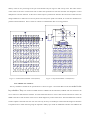
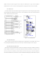
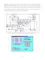
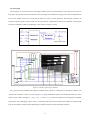
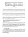
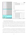
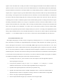
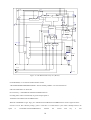
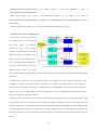
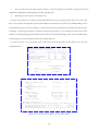
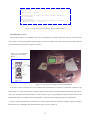
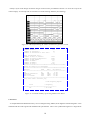
FACULTY OF ENGINEERING
–
INTEGRATED CIRCUITS LAB
ELECTRONICS AND COMMUNICATIONS DEPARTMENT
VLSI DESIGN AND IMPLEMENTATION OF THE
BASEBAND SECURITY CORE FOR BLUETOOTHTM WIRELESS
COMMUNICATION SYSTEM STANDARD
SUPERVISOR
PROF. DR. HANI F. RAGAAI
BY
AHMAD ABDELHAMEED
&
SAMEH ASSEM IBRAHIM
1. ABSTRACT
An FPGA solution for the Bluetooth security measures has been designed and implemented with 45 I/O ports and a
maximum clock frequency of 66MHz on Xilinix Virtex FPGA. We could achieve a single chip performing the key
generation and handling for authentication and encryption algorithms in addition to it’s own built-in pseudo random
number generator. The encryption core only was implemented and tested on Xilinix Spartan. All the simulation and
back annotation results were consistent with the sample data available within the Bluetooth specification.
2. SYSTEM OVERVIEW
Bluetooth is a new promising technology. The expectations for Bluetooth are huge. Analysts’ mark projections place
Bluetooth-enabled products in the “next big thing” category, with sales expected to top a billion units by 2005. It is a
technology to replace cables between any electronic devices. The technology is an open specification for wireless
communication of data and voice. It is based on a low-cost short-range radio link, built into a 9 x 9 mm microchip,
facilitating protected ad hoc connections for stationary and mobile communication environments.
The need for Bluetooth Security measures emerged from the fact that the standard works in the ISM band. Many
applications use this free band, which renders the environment noisy that data can be received from unauthorized users
and the transmitted data can suffer from eavesdropping as well. To avoid this, different security measures have been
taken into consideration in Bluetooth specifications.
Baseband Bluetooth Security has three main functions: Key generation and handling, Authentication and Encryption.
The design was targeted to perform the three functions. The order of running these functions and the interactions
between them is a higher level operation. However we managed to design a controller to perform these functions for
self consistency.
Some or all of these functions can be implemented in software but to increase speed of processing we aimed to get
them hard-wired. Bluetooth is finally a single chip transceiver. This implies to design the security core as an ASIC to be
embedded in that chip. However for testing and verification purposes an FPGA based design was our aim.
Verification was based on the sample data provided in the Bluetooth specifications. Also the different algorithms
used were implemented in software to generate random test vectors to be used.
3. SOFTWARE USED
1. FPGA Advantage: Renoir was used for design entry. VHDL codes, block diagrams and state diagrams were all
entered through it. The only problem we faced was combining the work of both of us together.
This forced us to rename all the libraries and files made to work together after working
separately.
1
Modelsim was used for simulation and backannotation. Inputs were taken from MATLAB and
outputs were compared with MATLAB outputs for verification.
Leonardo was used for synthesis and Xilinix FPGA’s were targeted.
2. Xilinix Alliance: That was the software used for placement and routing on the Xilinix FPGA’s and programming
them as well.
3. MATLAB: It was used to implement the algorithms in software and to generate testbenches for verifications.
4. THE IMPLEMENTED BLUETOOTH SECURITY CORE
According to the Bluetooth specifications ver.1.1, three main functions must be implemented within the security core.
These are:
1.
Key generation and management.
2.
Authentication.
3.
Encryption.
4.1. KEY GENERATION AND AUTHENTICATION
Four different algorithms are used to achieve these functions. These are E1 (for authentication), E21 and E22 (for link
and initialization key generation) and E3 (for encryption key generation). The four algorithms depends on an algorithm
called Ar and a slightly modified one called Ar’. Both Ar and Ar’ are based on the SAFER+ encryption algorithm. This
algorithm consists of 8 encryption rounds consisting of non linear operations. Each round has a 128 bits plaintext and 2
subkeys provided by a key scheduler. A final subkey is used for some extra operations.
4.1.1. SAFER+ ENCRYPTION ROUND IMPLEMNTATION
It was designed using the block diagram editor in Renoir. The small blocks in it like the modulo-256 adder, the 8-bit
XOR, PHT and Permute were designed as VHDL codes. But the exponential function [(45x mod 257) mod 256], where
x ranges from 0 to 255, and the logarithmic function [(log45(x) mod 257) mod 256], was very difficult to be
implemented as an algorithm in VHDL. MATLAB also was unable to calculate the function as well. So the values were
written as a look-up table (LUT) in VHDL. The round was designed in a pure combinational way made up of these
blocks just as stated in the specifications (figure 1). The advantage in this way is the single clock needed to do all the
round calculations. Unfortunately, the implementation of the overall chip shows how large its area was. The round was
redesigned to be a sequential one to avoid the repetition of look-up tables, which increases the area so much. The new
design made use of a controller entered as a 10 states finite state machine (FSM) with multiplexers and a demultiplexer
as shown in figure 2. The idea of the controller was to select each clock a different 16 bits of the input and the two
2
subkeys. Thus we are processing 16 bits per clock and thus only one log LUT and one exp LUT. The order of the 2
octets in the 16 bits were reversed each clock to follow the specifications. Thus the controller was designed to control
multiplexers to do this function. At the end a certain output is produced to announce the end of the round. This new
design enabled us to reduce the core area by about 25%. But yet the speed was reduced, as 8 clocks are needed now to
perform round calculations. Since it works on 128 bits a round therefore this is not a big problem.
rou nd_ inp ut : (127:0)
output
@
+
k2r_1 : (12 7:0)
round_input
e
log
+
@
pass
@
+
+
@
@
+
+
@
@
+
+
@
@
+
+
k2r : (12 7:0)
@
k2r_1
e
log
log
e
e
log
log
e
e
log
log
e
e
log
log
e
+
@
@
+
+
@
@
+
+
@
@
+
+
@
@
+
k2r
PHT
PHT
PHT
PHT
PHT
PHT
PHT
round_control
PHT
reg16oct
permute
PHT
PHT
PHT
PHT
PHT
PHT
PHT
PHT
PHT
PHT
PHT
PHT
PHT
PHT
PHT
PHT
PHT
PHT
PHT
PHT
PHT
PHT
PHT
PHT
PHT
PHT
PHT
permute
PHT
PHT
PHT
PHT
permute
PHT
PHT
PHT
PHT
PHT
PHT
permute
PHT
PHT
PHT
PHT
PHT
PHT
permute
permute
PHT
PHT
PHT
PHT
PHT
PHT
PHT
PHT
PHT
PHT
PHT
PHT
PHT
rou nd_ output : (12 7:0)
round_output
Figure 1: Combinational SAFER+ round (Renoir)
Figure 2: Sequential SAFER+ round (Renoir)
4.1.2. SAFER+ KEY SCHEDULE
The key schedule as needed in the specifications is shown in figure 3. Seventeen Bias words are needed in the
key scheduler. They were written in VHDL format as a ROM. On the other hand, a VHDL code was written for the
Octets summer to XOR the 8 bits of all the 16 octets and for the Rotator to octets 3 bits left. The selection of octets to be
added to the bias words was done in the Selector block diagram by certain connections. The bias ROM with seventeen
128 bits outputs at the same time was of no use since only two keys are needed per round. Thus the design was turned to
a sequential one to reduce the area giving the required 2 subkeys per round. No additional controller was added as the
3
SAFER+ controller was used. See figure 4. Yet new blocks were needed such as a register written in VHDL for
feedback and Octets rotator to rotate the octets among themselves for appropriate selection of octets to be added.
4.1.3. AR/AR’ BLOCK
A controller entered as a finite state machine using the state diagram editor was used to manage the eight rounds and
also the feedback paths to differentiate between Ar and Ar’. The only difference is that in the Ar’ function the input of
round 1 is added to the input of the 3rd round.
k1
octets_sum
feedback
+
+
+
+
+
+
+
+
+
+
+
+
+
+
+
+
ki : (127:0)
octets_rotate
octets_circulate
+
+
+
+
+
+
+
+
+
+
+
+
+
+
octets_rotate
octets_circulate
+
+
+
D Q
Figure 3: SAFER+ key schedule for 128 bit key
CLK
Q
+
kii : (127
+
+
+
+
D
+
+
+
+
+
+
+
+
+
+
k17
sel : (2:0)
reg136 bias_rom
Figure 4: Key scheduler(Renoir)
4.1.4. E1/E21/E22/E3 BLOCK
Another controller also entered using the state diagram editor was implemented to use the SAFER+ block as any of
the required algorithm depending on the value of a two bits input. The final block diagram is shown in figure 5.
4.1.5. E1/E21/E22/E3 BLOCK SIMULATION
The simulation of the design depended mainly on 2 things: An example given in the paper of SAFER+ nomination as
an AES candidate to simulate the Ar/Ar’ block, and the sample data in Bluetooth specifications to simulate the overall
block. Every small part was simulated by itself first and they all seemed to work properly. All the blocks should have
been all back annotated but only the small ones were back annotated and worked properly. Others didn’t fit except on
4
large FPGA’s not installed on Xilinix software at our hands. Then it was time to simulate the algorithms block
depending on the sample data and whether they are working correctly or not. To be sure that the block was working
well for other inputs too, we started to write a test bench for the design. A MATLAB GUI program creates random
inputs, evaluates the outputs of E1, E21, E22 and E3 algorithms, puts the inputs in a test vector and the outputs in a file
and finally compares this output file with another one produced by ModelSim.
key : (127:0)
ad_PIN_COFu : (47:0) bdadb_COFl : (47:0
Rand : (127:0)
Ran d(7: 0) : (12 7:0 )
a : ( 7: 0)
c : ( 7: 0)
b : ( 7: 0)
ou tput _4 : (7: 0)
e_ type(0) : (1: 0)
Concatenation
Ran d(12 7:8 ) :inp
(12ut7:0
: ()7: 0)
in_ 2 : (12 7:0 )
offset
in1 : (12 7:0 )
in2 : (12 7:0 )
sel
ou tput : ( 12 7:0 )
ou tput _7key
: (12
: ( 7:0
12 7:0
) )
in1 : (12 7:0 )
in2 : (12 7:0 )
sel
in2 : (12 7:0 )
ou tput _9 : (12 7:0 )
sel
ou tput : ( 12 7:0 )
ou tput : ( 12 7:0 )
sel
ou tput : ( 12 7:0 )
y
dash
ou tput : ( 12 7:0 )
ou tput _3 : (12 7:0 )
SAFER
dash
dash
e_ type : ( 1: 0)
done
start_algo
start_algo
ou tput _1 : (12 7:0 )
in2 : (12 7:0 )
rst
rst
e_type : (1:0)
in2 : (12 7:0 )
ou tput : ( 12 7:0 )
plain _text : ( 12 7:0 )
key : ( 12 7:0 )
rst
sel
in1 : (12 7:0 )
e_ type(1) : (1: 0)
ou tput _2 : (12 7:0 )
rst
in1 : (12 7:0 )
y
ou tput : ( 12 7:0 )
ou tput _8 : (12 7:0 )
in2 : (12 7:0 )
sel
in_ 2 : (12 7:0 )
in2 : (12 7:0 )
e_ type(0) : (1: 0)
sel
ou tput : ( 12 7:0 )
ou tput _7 : (12 7:0 )
in1 : (12 7:0 )
y
in1 : (12 7:0 )
e_ type(1) : (1: 0)
z
in2 : (12 7:0 )
in1 : (12 7:0 )
e_ type(0) : (1: 0)
algo_control
clk
done
go
clk
ciph er_ text : ( 12 7:0 )
ciph er_ text : ( 12 7:0 )
go
done
go
key_change
key_change
Ran d : ( 12 7:0 )
z
end_algo
inp ut1 : (12 7:0 )
clk
ou t_3 : (12 7:0 )
ou t_2 : (12 7:0 )
end_algo
end_algo
ou tputinp
: ( ut2
12 7:0
: (12
) 7:0 )
reg128
xor_128
ou tput _5 : (12 7:0 )
inp ut2 : (12 7:0 )
ou tput _6 : (12 7:0 )
ou tput : ( 12inp
7:0ut1
) : (12 7:0 )
add_128
algo_out : (127:0)
Figure 5: The block diagram that can be used for E1, E21, E22 and E3 algorithms (Renoir)
Figure6: The GUI MATLAB program written for testbench generation
5
4.2. Encryption
The encryption is carried out with a stream cipher called E0 that is re-synchronized for every payload. E0 consists of
three parts. One part performs the initialization where the input bits combined in an appropriate order and shifted them
into the four LFSRs used in the second and the main part, the key stream generator. The third part performs the
encryption and decryption. The key stream bits are generated by a method derived from the summation stream cipher
generator attributable to Massey and Rueppel. This is shown in figures 7 and 8.
Figure 7: stream ciphering with E0
Figure 8: the Encryption engine (Renoir)
The system uses linear feedback shift registers (LFSRs) whose outputs are combined by a summation combiner. The
output of this combiner is the key stream sequence, or, during initialization phase, the randomized initial start value.
There are four LFSRs of lengths L1 = 25, L2 = 31, L3 = 33 and L4 = 39 , with a total length of 128 and primitive feedback
polynomials with a Hamming weight of five, a reasonable trade-off between reducing the number of required XOR
gates in the hardware realization and obtaining good statistical properties of the generated sequences.
6
4.2.1. LFSR
LFSRs sequence through (2N –1) states, where N is the number of flip-flops in the LFSR. A value of all "1’s" is illegal
in the case of an XNOR feedback, and a value of all "0's" is illegal for XOR feedback. There are two implementation
styles of LFSRs, Galois implementation (figure 9) and Fibonacci implementation (figure 10). The first one was chosen
as it offered shorter time, smaller XOR size and modular design for best fitting in our FPGA. Although the early first
simulation showed that there was no need for set or rest inputs for the D-flip flop, the back annotation showed it not
working due to the presence of un-initialized bits.
Figure 9: Galois Implementation
Figure 10: Fibonacci Implementation
After the first 240-cycle, the LFSRs must be loaded with the last generated 128 bits. This means an added multiplexer
to each bit of the LFSRs. There were two choices which one come first: the MUX or the DFF? Both choices has worked
for the first 240 cycles successfully but there was a delay of one clock cycle when performing the parallel loading for
the last 128 generated bits when taking the input to the MUX first. So, the next configuration was chosen. When
“LOAD” (a control output from the FSM controller inside E0) is low, the INPUT passes to OUTPUT, but when it is
high; the parallel loading of the last 128 generated bits passes. As long as “INIT” (a reset input controlled by a higherlevel controller outside E0) is high, OUTPUT will stay low. It is clear that the structural way was chosen for
implementing the LFSRs as it gives the most perfect results as we are targeting the basic building blocks on the FPGA.
The behavioral one can also work but the synthesis with Leonardo showed additional gates like AND & OR gates.
The incoming bits must fill each LFSR first before closing its own feedback switch and here rises a problem: how to
design a feedback switch to be closed after 25 clock cycles for the LFSR1 for example? An AND gate is added in the
feedback path as shown to perform the AND operation on the feedback signal and a control signal “FB25” coming from
the FSM of the encryption engine: when it’s high, the switch is closed and the incoming feedback signal will pass. If
“FB25” is low, the output of the AND gate is low (logic ‘0’) and going to the input of the XOR gate at the input of the
LFSR to be XORed with IN25, which will pass to the first bit of the LFSR. The same idea was used for the other
LFSRs.
7
Figure11: the first LFSR (Renoir)
4.2.2. INPUT SHUFFLING
Let’s suppose that the KC, BD_ADDR and the CLK26-1 are coming in serial to reduce the number of pins. A finite
state machine can be used with an 8 bits counter while using a 3 x1 multiplexer at the input of each LFSR. This method
was proved to be complicated and slow and thus another methodology is used as long as this encryption engine shares
the same chip with other security algorithms. E0 will get the Key from E3 as a 128 bits parallel output. We get the
Bluetooth device address as a serial bit stream to be stored in a shift register shared between all the blocks and then E0
will get it as a parallel input. The CLK26-1 is coming out of the Bluetooth counter as a parallel output too. Then, two
registers of the length 49 and two of the length 55 are needed. A parallel loading will start when a control signal
“Load_reg” comes from the FSM of E0 while shifting is disabled. After that, the control signal (Load_reg) will go low
and shifting will start to the inputs of the four LFSRs. The parallel load will guide the incoming parallel inputs to their
positions. After all the bits being shifting in, we have three choices:
Insert a switch to disable the XOR gate at the input of the LFSR. A multiplexer should be used too.
The switch may come before the XOR gate with the same idea as the feedback switch.
Shift all zeros ‘0’ to the input.
Both ways 1 and 2 will need more gates and extra control signals for the switches and MUXs and these control
signals must be time based. This means additional states in the finite stat machine FSM, which will lead to an additional
D flip flop for each extra state. The last idea is used. Shifting the control signal (Load_reg) with the incoming data will
work as shifting a ‘0’ after all the bits being shifted in with just adding a wire from the control signal (Load_reg) to the
last position of the shift registers. Shifting will not start until (Load_reg) goes to ‘0’.
4.2.3. PARALLEL LOADING
At t=240, a parallel loading will be performed to the four LFSRs for the last generated 128 bits at a specified
positions to achieve a complicated shuffling. A 128 bits register with enabling and disabling its clock only once is used.
At t=240 a parallel load of the contents of this register will be performed on the four LFSRs at the specified positions
with an appropriate port mapping.
8
4.2.4. THE FINITE STATE MACHINE
We need this controller to manage the operation of different blocks in the Encryption Engine, which can be
summarized as follows:
1. Opening and closing of the feedback switches for the LFSRs at different clocks.
2. Resetting the blend registers when all switches are closed.
3. Keeping the contents of the blend register and the end of the initialization step.
4. Perform the parallel loading at the end of the initialization step.
It seems simple but it needs a very careful timing design. 7 control signals are needed controlled through the output of
an 8 bits counter, which will be reset when an encryption command is issued while no need to stop it. To reduce the
power consumption, the clock will be enabled/disabled through an And gate and a control signal according to whether
the encryption engine is in use or not.
4.2.5. ENCRYPTION ENGINE SIMULATION
Simulation was performed according to “Appendix IV” of the Bluetooth specification, Encryption Sample Data.
All the four sets of sample data with 364 clock cycles for each were obtained successfully. Figure12 shows the
waveforms obtained from Modelsim compared to the expected results from the first set of sample data. The waveform
is shown around t=240 when the parallel load is performed. For the purpose of simulation only, a 9-bits counter is
added to work in parallel with the 8-bits counter already exist in the design to show the clock number up to 364 which is
the last clock in the sample data and thus helps me to trace all the clocks in all the sets. A visual C++ program was also
used to verify some additional samples and the results were also O.K.
9
Figure 12: simulation results from ModilSim compared to the sample data taken from the Bluetooth specification
4.3. BLUETOOTH RANDOM NUMBER GENERATOR:
Each Bluetooth unit has a random number generator. Ideally, a true random generator based on some physical
process with inherent randomness is used. Examples of such processes are thermal noise from a semiconductor or
resistor and the frequency instability of a free running oscillator. For practical reasons, a software-based solution with a
pseudo-random generator is probably preferable. Clearly, the Link Manager (LM) can use such a generator for various
purposes; i.e. whenever a random number is needed. Bluetooth needs 7 different RAND numbers. However, these
numbers are to be sent over air in public during Authentication between two devices; these numbers are no more
secrets.
The most efficient implementation is to use an LFSR, which are the functional building blocks of circuits like the
pseudo-random noise (PN) code generator and Gold code generators commonly used in CDMA systems. The PN code
has a life time of 23 hours and 18 minutes. With a 3.2KHz BaseBand clock, we can calculate the length of the LFSR
required for a single bit random number to be 28 stages. However, different blocks in the Authentication and Key
generation algorithm needs the 128 bits random number as a parallel inputs. This forces us to use a 128 bits shift
10
register to store the number first. Actually, this leads to a much longer period besides the extra hardware and the slow
operation; we have to wait for 128 clock cycles for the random number to be stored and then perform the parallel input.
We have found that we should use a 128-stages LFSR as our random number generator. In addition to the 128 parallel
outputs, there is a single bit output to get the random number serially and send it outside our chip. When the Bluetooth
starts working, a reset signal will force the LFSR to be all zeros. Whenever we need a random number, a command will
be issued to make the parallel loading and starts counting 128 serially outputs at the same time. We have built some
controlling blocks to enable or disable the operation of the random number generator according to the situation requires
such things. Would that be random? Yes, as long as it is impossible to need two consecutive random numbers. It is also
possible to fill this LFSR with a serial number, which is actually the random number coming from the other Bluetooth
device. This will lead to more randomness. As a future work, we may make it possible to load our random number
generator with any parallel input from LM for example and not just by all zeros. According to the unpublished research
done by Wayne Stahnke while he was at Fairchild Semiconductor in 1970, there is a table to define the maximal length
sequence L = 2N-1 for LFSRs of length 3 to 168. For the N=128 bits, this is done with feedback at (128,126,101,9).
4.4. The Bluetooth Security Core
We thought of designing it to be able to deliver a single chip. Combining the E0, E1, E21, E22 and E3 was not that easy
task in the absence of a RAM. Every algorithm depends on the output of other algorithms. For example, E0 gets it Kc
from E3, which gets its COF from E1’s ACO or from the BD_ADDR. Again E1 gets its key from either E21 or E22. All of
the algorithms need a 128 bits random number and some of the algorithms inputs or outputs have to be sent to the other
user. To solve these problems we needed: A complicated controller designed as a FSM but was written in VHDL and
entered using Renoir. We believe this controller is doing some of the LM functions. We needed also some shift registers
to convert from serial to parallel and vice versa and so we were able to reduce the number of pins greatly. In addition,
we needed some multiplexers and registers. Some of the controller' functions are:
1.
According to the value of “e_select” entered, it issues some outputs to select the algorithm required as
well as opening the correct path.
2.
It stops all the operations as long as “en_fb” =’0’ or “load_adr” =’1’ or “load_key”=’1’. All this
conditions means that there’s an external input being added serially by the upper layer.
3.
It produces the required signals for the start and stop of operations of E0
4.
Together with another block written in VHDL called RNG control, it controls the random number as
required and stops it whenever an algorithm is running or whenever a random number is being added.
5.
It issues ‘start_algo’ required by the algorithm block.
6.
It issues outputs that tells the upper layer controller to start saving the output.
11
The multiplexers shown in figure 13 are used to select COF equals to ACO or obtained from the concatenation of
BD_ADDR when the used key is a mater one. It is also one of the functions of the controller to do it. Also the and gates
shown are used to disable the clocks on the shift registers whenever serial input has finished.
The core is now ready to be used with an upper layer controller to correctly input the data at correct times. And
correctly set the sequences of algorithms used as needed in different security levels.
The pins of the core and their functions are shown in table 1.
Pin Name
Function
Clk
To enter the external clock
Rst
To reset the core
Data_in
To enter the data to be encrypted
Data_out
The output of the encrypted data
cl26 (26
The 26 bits CL26 input to the encryption engine E0
pins)
e_select
(3 pins)
To select among various algorithms:
¾
“000” : E21
¾
“001” : E22
¾
“010” : E1
¾
“011” : E3 when key used is a master key
¾
“100” : E3 when key used is any other key
¾
“101” : E0 start
¾
“110” : E0 stop
¾
“111” : to be selected after any algorithm.
Note that: there are still the upper link manager that determines the sequence of algorithms
to be done after each other. And thus it is responsible for putting the values of these pins.
Load_adr
To start entering the addresses serially set this pin ‘high’ and when finished set it ‘low’
adda_pin
An address serial input or pin serial input as well.
Addb
Another address serial input.
Load_key
To start entering an external key serially put it ‘1’ else put it ‘0’
key_in
The input of the serial key
key_out
The output of the serial key
12
En_fb
Enables the feedback of the pseudo-random generator. Thus when it is ‘0’, no feedback is
present and its working as a shift register to have an external random number entered
serially.
Rand_in
The input of the external random number.
Rand_out
To output the random number used serially
Rand_start
To indicate the start of the random number used
out_start
To indicate the start of the output key or SRES
Sres_out
To output the SRES serially
Table 1: The pins of the core and their functions.
4.4.1. THE SIMULATION OF THE CORE:
Due to having the pseudo-random generator built in the core, the simulation was a very complicated task as the
random number used is not known. But thanks to the rand_start output the random number can be known.
Another problem appeared which is the impossibility of simulation of core when doing the E0 tasks due to not
knowing the outputs to be taken. That would have been the case for the other algorithms except for the help of the
MATLAB code written. So let’s try a sequence and test the core.
First we have to generate an initialization key. We start by resetting the whole core. And setting the e_select = ‘001’;
the code for E22. also we set load_adr = ‘1’ which means we’ll enter an address and a PIN code serially. But we’ll start
this after some time to have a good random number generated. Remember that en_fb should be = ‘1’ for the RNG to
operate. Load_key =’0’ cause we don’t have an external key.
After running the simulation for sometime , we have to enter the address and the PIN code serially. And after 48
clock cycles setting the load_adr=’0’. To add this data serially we’ll force a clock on both adda_pin and addb pins with
double the clock period one starting with a rising edge and the other with a falling one. This would make
PIN=’AAAAAAAAAAAA’ and address=’555555555555’. From ModelSim we see the random number used to be =’
00F4CC003B000003000000000007E000’. Taking these values and running the MATLAB program we get:
Kinit= ‘84FC3B8C9F1AE0A237F78D4E51685337’
Now let’s set e_select=’111’ and continue running till we get out_start=’1’ and take the value of K produced.
Kinit as produced by ModelSim =‘84FC3B8C9F1AE0A237F78D4E51685337’ which is the same as MATLAB.
Now , let’s perform an authentication function. The current link key is Kinit and we have a new random number and
the address we’ll take the value already entered. So let’s set e_select=’010’ and then ‘111’ after about 5 clocks. And run
the simulation. Notice that en_fb=’1’ , load_adr=’0’ and load_key=’0’ thus the algorithm will run as soon as e_select
=’010’.
13
load_key
key_in
en_fb
KEY_IN
CLK
clk
out_start
GET_KEY: (128 :1)
SAVE_KEY
rst
rand_in
RST
EN_FB
REG_128
CL K_REG 128
RNG
KEY_R EG : (128:1)
RAND_IN
rand_out
RAND_OUT
clk
ClK
RAND : (128 :1)
KEY_READY
key_out
CLK
KEY_R EG : (128 :1)
RAND : (128 :1)
ClK_RNG
KEY_OUT_SR
KEY_OUT
KEY_R EG : (128:1)
KEY_R EG : (128:1)
clk
Q
Q
clk
CLK
D
EN
RST
rst
rst
en_fb
start_algo
rst
ke y : (1 27:0)
rst
RNGcontrol
Rand : (1 27:0)
alg o_ou t : (1 27:0)
alg o _out( 127:96) : (127:0)
key_change
key_change
out_start
algorithm
end_algo
alg o_out : (127 :0)
clk
SRES_ IN : (32:1 )
out_start
sres_out
SRES_READY
e _ty pe : (1 :0 )
SRES_SR
CLK
clk
start_algo
SRES_OUT
clk
alg o_ou t(95:0 ) : (1 27:0)
ad_ PIN_CO Fu : (4 7:0)
bdadb_ COFl : (4 7:0)
out_start
ad_ PIN_CO Fubd
:a
(47
db
:0)
_COFl : (47:0)
ACO_ADDR : (48:1 )
REG96
SAVE_ACO
ACO_ADDR : (48:1)
C1
C1
C1
ACO_REG : (96:1)
ADDR_ REG : (48:1)
ACO_REG : (4 8:1)
controller
ADDR_ REG : (4 8:1)
ACO_REG : (48:1 )
ACO_REG(9 6:49) : (96:1)
ACO_REG(48:1) : (96:1 )
start_algo
rand_start
RST
E_ty p e : (1 0
:)
E_ ty pe : (1:0 )
ADDR_REG : (48:1)
B1 : (48:1)
start_algo
e_select : (2:0)
ADDR_ REG : (48:1)
ADDR_SR
E_ sele ct : (2 :0 )
CLK
out_start
ADDR_ REG : (48:1)
ADDR_SR
addA_PIN_addB
CLK
addA_PIN_addB
end_algo
C1
CLK_ADDR_REG
alg o _out : (127 :0)
OUTPUT
C1
data_in
clk
load_adr
clk
RAND_start
en_fb
en_fb
alg o_
algo
aout
g
l_
al
out
o_
(g
12
al
o7
g
( ut
_
11
al
out
:1
o_
g
(20
9:112
11
al
ou
o_out
g
()1
ao_
t::1
g
0
l(3:96)
95
)ou
04
o_out
(1
al
(::88
g
8)a
2t7:0
o_
(12
7
(:g
:80
l79
)ou
o_out
:(1
(g
)7
:7
:a
)(12
:0
2
1
(12
tg
7:0
:2
()al
63
7:0)
(127:0
:7:0
()a
:5
5o
(12
6
:48
)out
)al
(12
): o
)(7
(12
: ):0
)7:0
al
o_
l:64
ou
o_
g
tg
l(:5ut
_
47
o_
(7:0)
g
:4
39:32
a
o_
ut
g
0
l31
ou
o_
((127:0
:2
:23:16
)o
(12
t:4
(ut
)15
(12
:7:0)
():8
7:
(1
7
:0):0
)2
(12
7:0
: ): (1
7
(1
) :0
27:0
2)7:0)
)
load_key
load_adr
load_key
DATA
load_adr
INIT
INIT
CLK_Enable
CLK_Enable
data_out
Load_reg
Load_reg
E0
ADDR_ REG(8:1 ) : (48:1)
ADDR_ REG(16:9 ) : (4 8:1)
ADDR_ REG(24:1 7) : (48:1)
ADDR_ REG(32:2 5) : (48:1)
ADDR_ REG(40:3 3) : (48:1)
ADDR_ REG(48:4 1) : (48:1)
CLK
ADDR_ REG : (48:1)
CLK
clk
cl 2cl6(25
26
cl (2
2)cl6:4
(23
26
)cl(25:0)
:(1
26(7:
:1
cl(25
5
26
6
:8)
)(3:
:0)
4: ):0
(25
: (25
)(25:0)
:0
: :0)
(25
) :0)
clk
load_adr
adda_pin
addb
cl26 : (25:0)
Figure 13: The Bluetooth Security core (Renoir)
From ModelSim, we see that the random number used is
‘3D33000EC00000C00000000001F80001’ whereas the BD_ADDR=’ AAAAAAAAAAAA’
and from initialization we know that
the current key =’84FC3B8C9F1AE0A237F78D4E51685337’
So taking these values to MATLAB, we get the output equals to
‘E4E3F1F353C5CB21C8AC8C5DB6A45912’
Whereas in ModelSim we get: Algo_out=’ E4E3F1F353C5CB21C8AC8C5DB6A45912’ which is again the same.
Now let’s run E3, this is done by setting e_select =’100’ then ‘111’ after about 5 cycles. COF is already known to be
equal
to
‘53C5CB21C8AC8C5DB6A45912’
whereas
14
the
current
link
key
is
still
‘84FC3B8C9F1AE0A237F78D4E51685337’
the
random
number
as
seen
from
Kc
was
ModelSim is
equal
to
equal
to
‘001800000000003F000030FFF0003C00’
When
these
values
were
entered
to
the
MATLAB
program,
found
to
be
‘EE32029B7027864E43A223B430FD240C’. ModelSim gives ‘EE32029B7027864E43A223B430FD240C’ which is
again the same.
This is enough to clarify that the core is working alright from the simulation point of view..
4.5. BACK ANNOTATION AND FPGA TESTS:
In our design, we have demonstrated
how VHDL circuits can be optimized
for
FPGA
targets
by
adapting
descriptions styles to the available
resources, such as flip-flops, three-state
buffers and others. This affects coding
styles for many basic design blocks,
such as storage elements, multiplexers
and finite state machines. We were
Figure 14: Flow unique to Alliance and Leonardo Spectrum
targeting Xilinx FPGAs und using
Xilinx Alliance Series for performing place and route and timing analysis and then returning to Modelsim for back
annotation.
Unfortunately, there were none a single block small in size enough to be tested on the available FPGA chip
available at our hands; the Spartan S10PC84. Targeting a larger FPGA form Xilinx family was the solution to
perform the back annotation with delays on different blocks of the Bluetooth security chip. For the Encryption
Engine, it gives correct timing results for all sets of sample data. However, modifications could be made for the
Encryption Engine to be tested on S10PC84.
The major problem with the Encryption Engine was the 208 bits input signals and their corresponding registers. Only
61 input/output and 392 CLB flip flop were available in the Spartan S10PC84 (the other 256 flip flop cannot be
reduced). Although, we could make the back annotation and timing simulation using ModelSim and the simprim library
on a larger FPGA and find the results correct exactly for all the sample data comes with the Bluetooth specification, we
thought of some clever way to download the Encryption Engine on the S10PC84 and test it experimentally with two
choices:
15
1.
We can remove the input shift registers and get a serial input directly to the LFSRs. This idea was hard to
realize due to difficulties in synchronizing the inputs with the clock.
2.
Replacing the input registers with smaller ones.
We have noticed that the first and the second sample data are all zeros except for the first three or four bits. And
thus, we can replace the large shift registers with smaller ones with the size of 4 bits only. Parallel loading will be
performed for the first 4 bits. Then, shifting ‘0’ when all the four bits being shifted into the LFSR. This idea has three
advantages: (I) reducing the number of required CLB flip flop from208 to 16, (II) reducing the inputs by the same
amount, too, and (III) keeping synchronization between the clock and the shifting procedure. The only disadvantage
was the limitation to the first and the second sets of sample data only.
In what to follows, we are presenting some results from Leonardo Spectrum, Xilinx Alliance series and the
experimental tests.
***********************************************
Device Utilization for S10PC84
***********************************************
Resource
Used
Avail Utilization
----------------------------------------------IOs
32
61
52.46%
FG Function Generators 233
392
59.44%
H Function Generators
7
196
3.57%
CLB Flip Flops
294
392
75.00%
----------------------------------------------Using wire table: s10-3_avg
Clock Frequency Report
Clock
: Frequency
-----------------------------------CLK
: 55.3 MHz
Figure 15: Summary report from Leonardo spectrum
Device utilization summary:
Number of External IOBs
Flops:
Latches:
Number of Global Buffer IOBs
Flops:
Latches:
31 out of 61
0
0
1 out of 8
0
0
Number of CLBs
Total CLB Flops:
4 input LUTs:
3 input LUTs:
190
294
238
71
Number of PRI-CLKs
out
out
out
out
of
of
of
of
196
392
392
196
1 out of 4
50%
12%
96%
75%
60%
36%
25%
The Delay Summary Report
The Number of signals not completely routed for this design is: 0
The Average Connection Delay for this design is:
3.125 ns
The Maximum Pin Delay is:
17.316 ns
The Average Connection Delay on the 10 Worst Nets is: 9.417 ns
Figure 16: From the Place and Route report of Xilinx Alliance
16
Timing summary:
--------------Timing errors: 0
Score: 0
Constraints cover 1279 paths, 410 nets, and 1138 connections
(100.0% coverage)
Design statistics:
Minimum period: 37.875ns (Maximum frequency:
Maximum net delay: 17.316ns
26.403MHz)
Figure 17: From the Post Layout Timing Report of Xilinx Alliance
4.6. EXPERIMENTAL TESTS
The encryption engine in its modified version was downloaded into the FPGA and tested. The tests were performed
on the XS40 V1.4 board for Spartan S10PC84 (figure 18). We have taken some photos for the setup and the obtained
waveforms from the oscilloscope. (figures 19 and 20)
Figure 18: Arrangement of
components on the XS40
Board.
Figure 19: Arrangement of components on the XS40 Board.
As we have so many controllers in our core and their time performances are critical for a functional operation of the
whole design, we could connect all the controllers together for the purpose of back annotation and testing. The success
of the back annotation and timing analysis of these controllers gives a good indication about the other blocks in the
design which cannot be targeted on the available FPGA. A back annotation and testing were successfully done.
For the complete implementation of the design, we used Leonardo Spectrum to perform synthesis targeted on a larger
FPGA like Virtex v1000fg680. The obtained output report is shown in figure 21.
17
Finally a layout of the design was drawn using IC station but not provided here because it is out of the scope of the
contest category. A final chip area of 12.04 mm2 was achieved using AMS 0.6 µm technology.
Figure 20: CRO output showing the counter used and encryption key stream
Number of ports :
Number of nets :
Number of instances :
Number of references to this view :
Total accumulated area :
Number of Dffs or Latches :
Number of Function Generators :
Number of MUX CARRYs :
Number of MUXF5 :
Number of MUXF6 :
Number of gates :
45
776
63
0
2553
4948
1006
367
110
4752
**********************************************
Device Utilization for v1000fg680
**********************************************
Resource
Used
Avail
IOs
Function Generators
CLB Slices
Dffs or Latches
45
4948
2474
2553
512
24576
12288
24576
Utilization
---------------------------------------------8.79%
20.13%
20.13%
10.39%
---------------------------------------------Using wire table: xcv1000-6_avg
Clock Frequency Report
Clock
: Frequency
-----------------------------------clk
: 66.2 MHz
Figure 21: Leonardo summary report using Xilinix Virtex FPGA
5. SUMMARY
A complete Bluetooth Baseband security core was designed using VHDL, block diagrams and state diagrams. It was
simulated and the results agreed with the Bluetooth specifications. Then it was synthesized targeted on a large FPGA
18
(Xilinix Virtex). Part of the design (A modified encryption core) was downloaded on an available smaller FPGA
(Xilinix Spartan) and tested experimentally.
The core is capable of performing three main security functions; namely, key generation, authentication and
encryption.
6. REFERENCES
1.
"The Bluetooth Core Specifications, v.1.1" available at
http://www.bluetooth.com/developer/specification/Bluetooth_11_Specifications_Book.pdf
2.
Muller T. "Bluetooth Security Architecture", July 07, 1999. Online. Available.
http://www.bluetooth.com/developer/download/download.asp?doc=174
3.
Massey and Rueppel . Schneier B., Applied Cryptography, 2nd Ed., John Wiley & Sons Inc., 1996
4.
“Bluetooth Bluetooth Architecture Overview” by James Kardach Principle Engineer Bluetooth SIG Program
Manager. Intel Corporation Intel Corporation.
5.
“Nomination of SAFER+ as Candidate Algorithm for the Advanced Encryption Standard AES” submission
document of 12 June 1998
6.
Miia Hermelin: “Cryptographic properties of Bluetooth Combination Generator” Master’s Thesis
7.
“An Introduction to Cryptography” 1990-1999 Network Associates, Inc.
8.
Pong P. Chu and Robert E. Jones “Design Techniques of FPGA Based Random Number Generator”
Department of Electrical and Computer Engineering, Cleveland State University, Cleveland, Ohio 44115
NASA Glen Research Center, Cleveland, Ohio 44112
9.
P. Alfke, “Efficient Shift Registers, LFSR Counters, and Long Pseudo-Random Sequence Generators,” Xilinx
Application Note, 1995. http://university.xilinx.com/xapp/xapp052.pdf
10. Xilinx official web site http://www.xilinx.com/products/spartan2/index.htm
http://www.xilinx.com/products/logicore/alliance/tblpart.htm
11. “Spartan and Spartan-XL Series Data Sheet v1.5, 3/00” http://support.xilinx.com/partinfo/ds060.pdf
12. “LFSRs as Functional Blocks in Wireless Applications”
http://university.xilinx.com/xapp/xapp220.pdf
13. “XS40, XSP Board V1.4 User Manual” http://www.xess.com/FPGA/homepage.html
14. Michael Gschwind, Valentina Salapura “A VHDL Design Methodology for FPGAs”
15. A Mentor Graphics Seminar on FPGA with Leonardo Spectrum by Michael A. Bohm,
Chief Scientist for Exemplar Logic http://seminar.techonline.com/mentorg4/live.rpm
19