1
Digital Circuit Design Using Xilinx ISE Tools
Table of Contents
1. Introduction
2. Programmable logic devices: FPGA
3. Creating a new project in Xilinx ISE
3.1 Opening a project
3.2 Creating an Verilog input file for a combinational logic design
3.3 Editing the Verilog source file
4. Compilation and Implementation of the Design
5. Functional Simulation of Combinational Designs
5.1 Adding the test vectors
5.2 Simulating and viewing the simulation result waveforms
5.3 Saving the simulation results
6. Preparing and downloading bitstream for the Spartan FPGA
7. Testing a Digital logic circuit
7.1 Observing the outputs using the on-board LEDs and Seven Segment Display
8. Design and Simulation of sequential circuits using Verilog
9.1 Design of Sequential Circuits
9.2 Simulation of Sequential Circuits
9. Design and Simulation of Finite State machines in Verilog
10. Hierarchical circuit design using Modules
11. Post synthesis Timing simulation with Modelsim.
Appendix:
A. Verilog Hardware Modeling – Introduction to the Verilog Language.
B. Digilent BASYS board.
ptb/dkb 2013
1
EE 3320
1. Introduction
Xilinx Tools is a suite of software tools used for the design of digital circuits implemented
using Xilinx Field Programmable Gate Array (FPGA) or Complex Programmable Logic
Device (CPLD). The design procedure consists of (a) design entry, (b) compilation and
implementation of the design, (c) functional simulation and (d) testing and verification. Digital
designs can be entered in various ways using the above CAD tools: using a schematic entry tool,
using a hardware description language (HDL) – Verilog or VHDL or a combination of both. In
this lab we will only use the design flow that involves the use of Verilog HDL.
The CAD tools enable you to design combinational and sequential circuits starting with Verilog
HDL design specifications. The steps of this design procedure are listed below:
1. Create Verilog design input file(s) using template driven editor.
2. Compile and implement the Verilog design file(s).
3. Create the test-vectors and simulate the design (functional simulation) without using a
PLD (FPGA or CPLD).
4. Assign input/output pins to implement the design on a target device.
5. Download bitstream to an FPGA or CPLD device.
6. Test design on FPGA/CPLD device
A Verilog input file in the Xilinx software environment consists of the following segments:
Header: module name, list of input and output ports.
Declarations: input and output ports, registers and wires.
Logic Descriptions: equations, state machines and logic functions.
End: endmodule
All your designs for this lab must be specified in the above Verilog input format. Note that the
state diagram segment does not exist for combinational logic designs.
Software used: We will use Xilinix Tools (v13.3) and Digilent Adept.(v2.2.0) in this lab.
Hardware : We will use a BASYS2 kit from Digilent Inc. (with a Spartan FPGA from Xilinx) to
implement the designs.
2. Programmable Logic Device: FPGA
In this lab digital designs will be implemented in the Pegasus board which has a Xilinx Spartan
3E FPGA XC3S250E. This FPGA part belongs to the Spartan family of FPGAs. These devices
come in a variety of packages. We will be using devices that are packaged in 208 pin package
with the following part number: XC2S50-PQ208. This FPGA is a device with about 250K gates.
Detailed information on this device is available at the Xilinx website.
ptb/dkb 2013
2
EE 3320
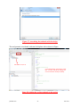
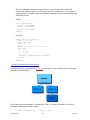
3. Creating a New Project
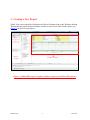
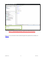
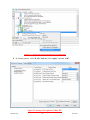
Xilinx Tools can be started by clicking on the Project Navigator Icon on the Windows desktop.
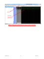
This should open up the Project Navigator window on your screen. This window shows (see
Figure 1) the last accessed project.
Process
window
Summary window
Figure 1: Xilinx ISE Project Navigator window (snapshot from Xilinx ISE software)
ptb/dkb 2013
3
EE 3320
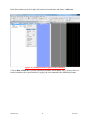
3.1 Opening a project
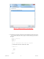
Select File->New Project to create a new project. This will launch the New Project Wizard
(Figure 2) on the desktop. Fill up the necessary entries as follows:
Figure 2: New Project Wizard (snapshot from Xilinx ISE software)
Name:
Write the name of your new project (E.g.: or_gate)
Location: The directory where you want to store the new project
Working Directory: The directory where all your project related files will be saved.
Description: (Optional) A brief description of your project
Leave the top level module type as “HDL”.
Example: If the project name were “or_gate”, enter “or_gate” as the project name and then click
“Next”.
ptb/dkb 2013
4
EE 3320
Clicking on NEXT should bring up the Project Settings window:
Ensure that these values are correct!
Figure 3: New Project Wizard- Project settings
For each of the properties given below, click on the ‘value’ area and select from the list of values
that appear.
o Device Family: Family of the FPGA used. In this laboratory we will be using the
Spartan3E FPGAs
ptb/dkb 2013
5
EE 3320
o Device: The number of the FPGA device. Note the device number on the FPGA
on the Digilent board! If you are unsure –ask the TA!
Check your board for the device number
o Package: The type of package with the number of pins. The Spartan FPGA used
in this lab is packaged in C6DGQ (which is equivalent to CPG132) package. If
you are unsure, ask the T.A!
o Speed : The Speed grade is “-4”.
ptb/dkb 2013
6
EE 3320
o Synthesis Tool: XST [VHDL/Verilog]
o Simulator: The tool used to simulate and verify the functionality of the design.
Choose ISim as the simulator.
Then click on NEXT to save the entries. The Project Summary window (Figure 4) will show you
a summary of your project details. In this example we have used the project name “or_gate”.
Pay attention to the highlighted details in particular!
Figure 4: New Project Wizard- Project Summary (snapshot from Xilinx ISE software)
Click on ‘Finish’.
All project files such as schematics, netlists, Verilog files, VHDL files, etc., will be stored in a
subdirectory with the project name. A project can only have one top level HDL source file (or
schematic). Modules can be added to the project to create a modular, hierarchical design (see
Section 9).
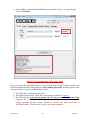
In order to open an existing project in Xilinx Tools, select File->Open Project to show the list
of projects on the machine. Choose the project you want and click OK.
ptb/dkb 2013
7
EE 3320
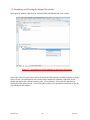
Figure 5: Create New source window (snapshot from Xilinx ISE software)
If you would like to create a new source file, from the ISE window, right click on the project
name and choose ‘New source’ or click on the New source button on the toolbar as shown in
Figure 5. You may also choose Project-->New Source from the menu.
3.2 Creating a Verilog HDL input file for a combinational logic design
In this lab we will enter a design using a structural or RTL description using the Verilog HDL.
You can create a Verilog HDL input file (.v file) using the HDL Editor available in the Xilinx
ISE Tools (or any text editor).
If adding an already existing source file (.v file) to the project, in the project Navigator window,
select Project -> Add Copy Source and browse through the disk for the source file.
If creating a new source file, in the Project Navigator window, select Project -> New Source.
A window pops up as shown in Figure 6. (Note: “Add to project” option is selected by default. If
you do not select it then you will have to add the new source file to the project manually.)
ptb/dkb 2013
8
EE 3320
Figure 6: New Source Wizard -creating Verilog-HDL source file (snapshot from
Xilinx ISE software)
Select Verilog Module and in the “File Name:” area, enter the name of the Verilog source file
you are going to create. Also make sure that the option Add to project is selected so that the
source need not be added to the project again. Then click on Next to accept the entries. This pops
up the following window (Figure 7).
ptb/dkb 2013
9
EE 3320
Figure 7: Define Verilog module window (snapshot from Xilinx ISE software)
In the Port Name column, enter the names of all input and output pins and specify the Direction
accordingly. A Vector/Bus can be defined by entering appropriate bit numbers in the MSB/LSB
columns. Then click on Next> to get a window showing all the new source information (Figure
8).
ptb/dkb 2013
10
EE 3320
Figure 8: New Source Wizard window(snapshot from Xilinx ISE software)
Once you click on Finish, the source file will be displayed in the sources window in the Project
Navigator (Figure 1).
If a source has to be removed, just right click on the source file in the Sources in Project
window in the Project Navigator and select Remove in that. Then select Project -> Delete
Implementation Data from the Project Navigator menu bar to remove any related files.
3.3 Editing the Verilog source file
The source file will now be displayed in the Project Navigator window (Figure 9). The source
file window can be used as a text editor to make any necessary changes to the source file. All the
input/output pins will be displayed. Save your Verilog program periodically by selecting the
File->Save from the menu. You can also edit Verilog programs in any text editor and add them
to the project directory using “Add Copy Source”.
ptb/dkb 2013
11
EE 3320
Figure 9: Verilog Source code editor window in the Project Navigator (from Xilinx ISE software)
Adding Logic in the generated Verilog Source code template:
A brief Verilog Tutorial is available in Appendix-A. For the language syntax and for
construction of logic equations please refer to Appendix-A.
The Verilog source code template generated shows the module name, the list of ports and
also the declarations (input/output) for each port. Combinational logic code can be added
to the verilog code after the declarations and before the endmodule line.
For example, an output z in an OR gate with inputs a and b can be described as,
assign z = a | b;
Remember that the variable names are case sensitive.
Other constructs for modeling a logic function:
A given logic function can be modeled in many ways in verilog. Verilog offers numerous
constructs to efficiently model designs. Here is an example in which a 4x1 multiplexer, is
implemented using a case statement:
ptb/dkb 2013
12
EE 3320
module mux4x1 (a,b,c,d,sel,y);
input a, b, c, d;
input [1:0] sel;
output y;
reg y;
always @ (a or b or c or d or sel)
case (sel)
0 : y = a;
1 : y = b;
2 : y = c;
3 : y = d;
default : y=1’b0; //One bit binary value ‘0’
endcase
endmodule
In the example shown, “sel” is the 2 bits wide select input to the multiplxer. The ‘default’
case in the case statement is reached when the variable value does not match any of the
case options.
The 4x1 multiplexer can also be implemented using a set of if-then-else constructs as
follows:
module mux4x1 (a,b,c,d,sel,y);
input a, b, c, d;
input [1:0] sel;
output y;
reg y;
always @ (a or b or c or d or sel)
if(sel == 2'b00)
y=a;
else if (sel ==2'b01)
y=b;
else if (sel ==2'b10)
y=c;
else if (sel ==2'b11)
y=d;
else
y=1'b0;
endmodule
Even though both the code segments shown above realize a 4x1 multiplexer, each one of
them leads to a different hardware implementation for the given logic. Explaining the
hardware implementations for specific Verilog construct is beyond the scope of this
document. Interested readers can refer to the links in the Verilog tutorial available in
Appendix-A.
ptb/dkb 2013
13
EE 3320
4. Compilation and Implementation of the Design
The design has to be compiled and implemented before it can be checked for correctness, by
running functional simulation or downloaded onto the prototyping board. With the top-level
Verilog file opened (can be done by double-clicking that file) in the HDL editor window in the
right half of the Project Navigator, and the view of the project being in the Module view, the
Implement Design option can be seen in the Process Window. Design Entry Utilities and
Generate Programming File options can also be seen in the process view. The former can be
used to include user constraints, if any and the latter will be discussed later.
To compile the design, expand the Implement Top Module (Figure 10) by clicking on Process>Implement Top Module OR by right clicking on the design and choosing Implement Top
Module. It will go through steps like Check Syntax, Compile Logic, Interpret Feedbacks,
Reformat Logic and Optimize Hierarchy. If any of these steps could not be done or done with
errors, it will place a
mark in front of that, otherwise a tick mark
will be placed after
each of them to indicate the successful completion. If everything is done successfully, a
mark will be placed before the Synthesize-XST option. If there are warnings, one can see
mark in front the Console window present at the bottom of the Navigator window. Every time
the design file is saved; all these marks disappear asking for a fresh compilation.
Clicking this is equivalent to
selecting the ‘Implement
Top Module’ option.
Active process list
Figure 10: Implement Top Module option in Xilinx ISE
ptb/dkb 2013
14
EE 3320
Figure 12 : Implementing the Design (snapshot from Xilinx ISE software)
If there are no errors then the tool shows that the design has been synthesized successfully as in
Figure 12.
ptb/dkb 2013
15
EE 3320
5. Functional Simulation of Combinational Designs
5.1 Creating a Testbench
To check the functionality of a design, we have to apply test vectors and simulate the circuit. In
order to apply test vectors, a testbench file is written. Essentially it will supply all the inputs to
the module designed and can check the outputs of the module. Example: For the 2 input OR
Gate, the test bench is created as follows:
1. Right click on the design (or_gate) and select New Source
Figure 13 : Adding a test bench to your design-step1
2. From the new source wizard pop up, select Verilog Test Fixture and enter a
name for the test bench (eg: or_tb) in the File name field as shown in the Figure
and click Next.
ptb/dkb 2013
16
EE 3320
Figure 14 : Adding a test bench to your design-step 2
3. The New source wizard will show the design that the test bench is associated with
(this should be the design that you wish to simulate- in this case, or_gate). Click
Next and then Finish.
ptb/dkb 2013
17
EE 3320
Figure 15 : Adding a test bench to your design-step 3
4. The ISE project navigator will generate some boilerplate test bench code for you
– you may either modify this code or replace it with the following code. Refer to
the Figure
module or_tb(a,b,z);
output a;
output b;
input z;
reg a,b; //declaration that a and b are registers
// Instantiate the Unit Under Test (UUT)
or_gate uut (
.a(a),
.b(b),
.z(z)
);
initial
begin
ptb/dkb 2013
18
EE 3320
//test stimuli
a <= 1’b0;
b <= 1’b0;
#100;
a <= 1’b0;
b <= 1’b1;
#100;
a <= 1’b1;
b <= 1’b0;
#100;
a <= 1’b1;
b <= 1’b1;
#100;
end
endmodule
Figure 16: Simulation window in ISE showing the newly created test bench.
ptb/dkb 2013
19
EE 3320
5.2 Simulating and Viewing the Output Waveforms
In the process window right click on Simulate Behavioral Model and click on Run.
Figure 17 : Launching the iSIM simulator from Project Navigator
If the code is free of syntax errors, this will launch the ISim simulator window as shown in figure
(Note; In case you encounter an error when trying to launch the simulator, right click on the
design and ensure that “manual compile order’ is not checked). Also make sure that the test
bench passes the syntax checks. You will be able to observe the simulation waveforms as per the
test stimulus in this window.
ptb/dkb 2013
20
EE 3320
Figure 18 : The iSIM simulator window- behavorial simulation for or_gate design
ptb/dkb 2013
21
EE 3320
6. Preparing and downloading bitstream file for the Spartan
FPGA:
A bitstream file needs to be prepared for each design and downloaded onto the Digilent
prototyping board.
6.1 Generating a User Constraint File
In order to test the design in the Digilent board, the inputs need to be connected to the
switches/buttons on the board and the outputs need to be connected to the onboard LED’s. This
is specified by a “User Constraint File (ucf file). To create a UCF for your design do the
following:
Figure 19: Launching XilinxPlanAhead from Xilinx ISE
Double click on the Floorplan Area/IO/Logic(Plan Ahead) option in the process window. This
will launch the Xilinx Plan Ahead tool.
ptb/dkb 2013
22
EE 3320
Setting switches (SW0, SW1) as inputs and
LED0 as output.
Figure 20: Assigning pins to inputs/outputs in Xilinx PlanAhead.
In the PlanAhead window shown in Figure 14, click on the nets that are assigned to the design
(in this case a, b, z) and in the I/O ports window assign the pin number aliases as specified on the
Digilent board.
Refer to I/O pin mapping information for the Digilent board.
o For the OR_GATE example, the user constraints may be specified as follows:
We can use switches SW0 and SW1 on the Digilent board as inputs (a and b) and
LED0 as the output (z). Note that:
Pin P11 and L3 are FPGA pins connected to SW0 and SW1 on the Digilent Board
Pin M5 of the FPGA is connected to LED0 on the Digilent Board.
ptb/dkb 2013
NET "a" LOC = P11;
Input a connects to SW0 (pin P11 on FPGA)
NET "b" LOC = L3;
Input b connects to SW1 (pin L3 on the
FPGA)
NET "z" LOC = M5;
Output z connects to LED0 (pin M5 on the
FPGA)
23
EE 3320
You can use this option to manually
edit the ucf file
Figure 21: User Constraint File (snapshot from Xilinx ISE software)
You may verify the generated UCF file by clicking on or_gate.ucf in the Design window in ISE.
If you would like to modify the UCF file manually ( to change the switches etc.) you may do so
by clicking on the Edit Constraints(Text) option in the Process window (Figure 15)
6.2 Generating a Bit Stream file (.bit)
In order to program the FPGA, you will need to generate a bit stream file of your design. In the
Xilinix ISE process window:
a. Right click on Generate Programming File and select Process Properties.
ptb/dkb 2013
24
EE 3320
Figure 22: Setting the Process Properties in Xilinx ISE.
b. In ‘Startup options’ select JTAG Clock and click “Apply” and then “OK”.
Figure 23: Setting CLK option on Xilinx ISE.
ptb/dkb 2013
25
EE 3320
c. Double click on ‘Generate Programming file’ (or right click and choose Run).
Figure 24: Generating a bistream file for your design.
This will generate a bitstream file that you can use to program the FPGA.
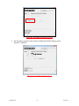
6.2 Programming the Digilent Board using Adept:
To program the FPGA on the Digilent board, do the following:
Connect the Digilent board to the USB cable (make sure the switch is set to ‘ON’
position).
Launch the Digilent Adept tool (Start->All Programs->Digilent->Adept)
ptb/dkb 2013
26
EE 3320
Figure 25: The USB connector and Power switch on the Digilent BASYS board.
This shows the FPGA version
automatically - this should match
the version on your board
Figure 26: The Digilent Adept window
ptb/dkb 2013
27
EE 3320
Click on Browse and select the bitfile that you generated in step 6.1 (or_gate.bit) and
click on “Program”
Figure 27: Programming the FPGA using Adept
Now you can test the functional behavior of your design on the FPGA using the switches and
LEDS on the BASYS board. Ensure that the “Programming Successful” message appears in the
message window. If you face problems please ensure:
The USB cable is connected to the board.
The board is powered ON. Check the switch settings as shown in Figure 19.
The FPGA device on the board matches the one that you specified in your design
properties. Eg. XC3S250E or XC3S100E. Note that if there is a mismatch you will
usually encounter an error stating “Unable to associate file with device due to
IDCODE conflict”. If this occurs, re check your design properties.
ptb/dkb 2013
28
EE 3320
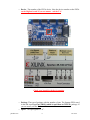
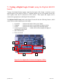
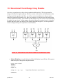
7. Testing a Digital Logic Circuit (using the Digilent BASYS
board)
Testing a downloaded design requires connecting the inputs of the design to switches or ports
and the outputs of the design to LEDs or 7-segment displays. In case of sequential circuits, the
clock input(s) must also be connected to clock sources. These inputs and outputs can be
connected to appropriately on the Digital Lab workbench.
The Digilent BASYS board used in the Digital Circuits lab has the following features, which
can be used to test the digital logic in the design:
1.
2.
3.
4.
8 Switches
-- which can be used to drive up to 8 inputs
4 Buttons
-- which can be used as reset signals (or) input switches
8 LEDs
-- which can be used to display up to 8 design outputs
4 Seven segment displays
-- which can be used to display four digits of
information on the board
5. Mini USB interface
6. Power on switch
5
3
4
6
2
1
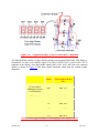
Figure 28: The Digilent BASYS board with Spartan 3 FPGA
ptb/dkb 2013
29
EE 3320
Figure 29: Digilent BASYS Board Architecture (www.digilentinc.com)
In order to use the respective input/output device on the board, the pin number of the device must
be connected properly to the design’s input/output. On the Digilent board, the pin number of
these inputs/outputs is as follows:
Input
Switches
Button
ptb/dkb 2013
FPGA Pin
(To be used in the ucf
file)
SW0
pin# M4
SW1
pin# L3
SW2
pin# K3
SW3
pin# B4
SW4
pin# G3
SW5
pin# F3
SW6
pin# E2
SW7
pin# N3
BTN0
pin# G12
BTN1
pin# C11
BTN2
pin# M4
BTN3
pin# A7
30
EE 3320
LD0
FPGA Pin
(To be used in the ucf
file)
pin# M5
LD1
pin# M11
LD2
pin# P7
LD3
pin# P6
LD4
pin# N5
LD5
pin# N4
LD6
pin# P4
LD7
pin# G1
Output
LED
Table 1: Pin mapping on the Digilent BASYS board
7.1 Observing outputs using the on-board LEDs and Seven Segment Displays
The Digilent board has four on-board 7-segment displays (see Figure 22) that are connected to
the corresponding on-board Spartan 3E FPGA chip. This display can be used to observe the
outputs of your design without using any additional wires if the design conforms to the pin
assignments for the on-board 7-segment display. Figure 22 shows the 7-segment display with the
conventional labeling of individual segments.
ptb/dkb 2013
31
EE 3320
Figure 30: 7-segment display (source: Basys user’s manual)
The Digilent board contains a 4-digit common anode seven-segment LED display. The display is
multiplexed, so only seven cathode signals (CA,CB,CC,CD,CE,CF,CG) exist to drive all 28
segments in the display. Four digit-enable signals (AN0, AN1, AN2, AN3) drive the common
anodes, as shown in Figure 22 and these signals determine which digit the cathode signals
illuminate.
Output
LED Anode
(To be used to
Multiplex between
Four Displays)
FPGA Pin
(To be used in the ucf
file)
AN0
pin# F12
AN1
pin# J12
AN2
pin# M13
AN3
pin# K14
CA
pin# L14
CB
pin# H12
CC
pin# N14
CD
pin# N11
CE
pin# P12
CF
pin# L13
LED Cathode
CG
pin# M12
Table 2: Seven segment display LED mapping on the Digilent board
ptb/dkb 2013
32
EE 3320
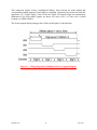
This connection scheme creates a multiplexed display, where driving the anode signals and
corresponding cathode patterns of each digit in a repeating, continuous succession can create the
appearance of a 4-digit display. Each of the four digits will appear bright and continuously
illuminated if the digit enable signals are driven low once every 1 to 16ms (for a refresh
frequency of 1KHz to 60Hz).
The Seven segment display timing to drive all the four displays is shown below:
Figure 31: Timing diagram for Multiplexed Seven Segment Displays
ptb/dkb 2013
33
EE 3320
8. Design and Simulation of Sequential Circuits using
Verilog HDL
The procedure to create Verilog design files for sequential circuits in Xilinx ISE is the same as
that for combinational circuits. The main difference between combinational and sequential
designs is the presence of flip-flops (registered outputs or nodes in the Declaration section of a
sequential design).
8.1 Design of Sequential Circuits
For large, complex state machines it is easier to specify them as programs. A sequential circuit
can be described either as a procedural block or a state machine in Verilog.
1. A D-flip with asynchronous reset can be modeled as a Procedural block as follows:
module dff_async (data, clock, reset, q);
input
data, clock, reset;
output q;
reg
q;
// logic begins here
always @(posedge clock or reset)
if(reset == 1'b0)
q <= 1'b0;
else
q <= data;
endmodule
ptb/dkb 2013
34
EE 3320
2. A D-flip with synchronous reset can be modeled as a Procedural block as follows:
module dff_sync (data, clock, reset, q);
input
data, clock, reset;
output q;
reg
q;
// logic begins here
always @(posedge clock)
if(reset == 1'b0)
q <= 1'b0;
else
q <= data;
endmodule
8.2 Simulation of sequential designs
Except for the additional clock signal, simulation of sequential designs can be done using
test_bench in the same way it was done for combinatorial circuits. The clock signal can be
generated in the test bench using a simple initial block as follows:
module test_bench(clk)
output clk;
reg clk;
initial begin
clk = 0;
forever begin
#5 clk = ~clk; //Time period of the clock is 10 time units.
end
// rest of the logic
endmodule
ptb/dkb 2013
35
EE 3320
9. Design and Simulation of Finite State machines in
Verilog.
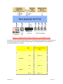
Basically a Finite State Machine (FSM) consists of a combinational logic, sequential logic and
output logic. Where combinational logic is used to decide the next state of the FSM, sequential
logic is used to store the current state of the FSM.
Types of State Machines There are many ways to code finite state machines, but before we get
into the coding styles, it is important to understand the basics.
There are two types of state machines, Mealy and Moore:
Source: EE3320 – Digital Circuits course slides
Depending on the need, either type of state machine can be used.
Encoding Style Since the state machine needs to be represented as a digital circuit, the states
can be represented by the following ways:
Binary encoding : In this each of the state is represented in binary code (i.e. 000, 001,
010....)
Gray encoding : In this each of the state is represented in gray code (i.e 000, 001, 011,...)
One Hot : In this only one bit is high and rest are low(i.e. 0001, 0010, 0100, 1000)
One Cold : In this only one bit is low, rest are high (i.e. 1110,1101,1011,0111)
9.1 State Machine Design in Verilog
State machine design in Verilog is illustrated with the following example.
Example: Use Verilog HDL to design a sequence detector with one input X and one output Z.
The detector should recognize the input sequence “101”. The detector should keep checking for
the appropriate sequence and should not reset to the initial state after it has recognized the
sequence. The detector initializes to a reset state when input, RESET is activated.
For example, for input X
= “…110110101…”,
FSM output Z = “…000100101…”
ptb/dkb 2013
36
EE 3320
9.1.1 Moore State Machine Example:
The state machine diagram of the Moore State machine for sequence detector example is shown
below:
`define CK2Q 5 // Defines the Clock-to-Q Delay of the flip-flop
module moore_fsm(reset,clk,in_seq,out_seq);
input reset;
input clk;
input in_seq;
output out_seq;
reg out_seq;
//-------------Parameters defining State machine States-----------------------------------parameter SIZE = 4;
parameter S0 = 4'b0001 , S1 = 4'b0010 , S2 = 4'b0100, S3 = 4'b1000;
//-------------Internal Variables---------------------------------------------------------reg
[SIZE-1:0]
state
;// Seq part of the FSM
reg
[SIZE-1:0]
next_state
;// combo part of FSM
//----------Moore State machine Code starts Here-----------------------------------------// Determine the next state for each state in the state machine using the input
// sequence given to it. The output next_state is combinatorial in nature.
//-----------------------------------------------------------------------------------------always @ (state or in_seq)
begin : FSM_COMBO
next_state = 4'b0001;
case(state)
S0 : if (in_seq == 1'b1) begin
next_state = S1;
end
else begin
next_state = S0;
end
S1 : if (in_seq == 1'b0) begin
next_state = S2;
end
else begin
next_state = S1;
end
S2 : if (in_seq == 1'b1) begin
next_state = S3;
end
else begin
next_state = S0;
end
S3 : if (in_seq == 1'b1) begin
next_state = S1;
end
else begin
next_state = S2;
ptb/dkb 2013
37
EE 3320
end
// Always include a Default state in your state machine.
default : next_state = S0;
endcase
end
//-----------------------------------------------------------------------------------------// Register the combinatorial next_state output.
//-----------------------------------------------------------------------------------------always @ (posedge clk)
begin : FSM_SEQ
if (reset == 1'b0) begin
state <= #`CK2Q S0;
end
else begin
state <= #`CK2Q next_state;
end
end
//-----------------------------------------------------------------------------------------// Based on the current state only, determine the output “out_seq”
//-----------------------------------------------------------------------------------------always @ (state or reset)
begin : OUTPUT_LOGIC
if (reset == 1'b0) begin
out_seq <= #`CK2Q 1'b0;
end
else begin
case(state)
S0 : begin
out_seq <= 1'b0;
end
S1 : begin
out_seq <= 1'b0;
end
S2 : begin
out_seq <= 1'b0;
end
S3 : begin
out_seq <= 1'b1;
end
default : begin
out_seq <= 1'b0;
end
endcase
end
end // End Of Block OUTPUT_LOGIC
endmodule // End of Module Moore state machine
//------------------------------------------------------------------------------------------
Except for the additional clock signal, simulation of finite state machines can be done using a
test_bench in the same way it was done for combinatorial circuits. The following is a sample
test-bench for the Moore state machine. The same can be used to test the Mealy state machine as
well.
//-----------------------------------------------------------------------------------------module sm_tb(reset,clk,in_seq,out_seq);
output reset;
output clk;
output in_seq;
input out_seq;
reg clk;
reg reset;
reg [15:0] data;
reg in_seq;
integer i;
ptb/dkb 2013
38
EE 3320
// The input data sequence is defined in the vector “data”
// Each clock one bit of data is sent to the state machine
// which will detect the sequence “101” in this data.
initial
begin
data = 16'b0010100110101010;
i = 0;
reset = 1'b0;
#1200 ;
reset = 1'b1;
#60000;
$finish;
end
// Clock Generation
initial
begin
clk = 0;
forever begin
#600 ;
clk = ~clk;
end
end
// Right shifting of data to generate the input sequence
always @(posedge clk)
begin
#50;
in_seq = data >> i;
i = i+1;
end
endmodule
//------------------------------------------------------------------------------------------
A top level module is required to stitch the state machine to the test bench.
//-----------------------------------------------------------------------------------------module top();
wire clk,reset;
wire in_seq,out_seq;
moore_fsm fsm0(reset,clk,in_seq,out_seq);
sm_tb fsm_tb(reset,clk,in_seq,out_seq);
endmodule
//------------------------------------------------------------------------------------------
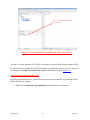
The operation of the Moore state machine is shown in the waveform below:
ptb/dkb 2013
39
EE 3320
9.1.2. Mealy State Machine Example:
The state machine diagram of the Mealy State machine for sequence detector example is shown
below:
`define CK2Q 5
// Defines the Clock-to-Q Delay of the flip flop.
module mealy_fsm(reset,clk,in_seq,out_seq);
input reset;
input clk;
input in_seq;
output out_seq;
reg out_seq;
reg in_seq_reg;
//-------------Parameters defining State machine States-----------------------------------parameter SIZE = 3;
parameter S0 = 3'b001 , S1 = 3'b010 , S2 = 3'b100;
//-------------Internal Variables---------------------------------------------------------reg
[SIZE-1:0]
state
;// Seq part of the FSM
reg
[SIZE-1:0]
next_state
;// combo part of FSM
//----------Register the input-----------------------always @ (posedge clk)
begin : REG_INPUT
if (reset == 1'b0) begin
in_seq_reg <= #`CK2Q 1'b0;
end
else begin
in_seq_reg <= #`CK2Q in_seq;
end
end
//----------Mealy State machine Code starts Here------------------------------------------// Determine the next state for each state in the state machine using the input
// sequence given to it. ‘next_state’ is combinatorial in nature.
//-----------------------------------------------------------------------------------------always @ (state or in_seq_reg)
begin : FSM_COMBO
next_state = 3'b000;
case(state)
S0 : if (in_seq_reg == 1'b1) begin
next_state = S1;
end
else begin
next_state = S0;
end
ptb/dkb 2013
40
EE 3320
S1 : if (in_seq_reg == 1'b0) begin
next_state = S2;
end
else begin
next_state = S1;
end
S2 : if (in_seq_reg == 1'b1) begin
next_state = S1;
end
else begin
next_state = S0;
end
default : next_state = S0;
endcase
end
//-----------------------------------------------------------------------------------------// Register the combinatorial next_state variable.
//-----------------------------------------------------------------------------------------always @ (posedge clk)
begin : FSM_SEQ
if (reset == 1'b0) begin
state <= #`CK2Q S0;
end
else begin
state <= #`CK2Q next_state;
end
end
//-----------------------------------------------------------------------------------------// Based on the combinatorial next_state signal and the input sequence, determine the output
// out_seq of the finite state machine.
//-----------------------------------------------------------------------------------------always @ (state or in_seq_reg or reset)
begin : OUTPUT_LOGIC
if (reset == 1'b0) begin
out_seq <= 1'b0;
end
else begin
case(state)
S0 : begin
out_seq <= 1'b0;
end
S1 : begin
out_seq <= 1'b0;
end
S2 : begin
if (in_seq_reg == 1'b1)
out_seq <= 1'b1;
else
out_seq <= 1'b0;
end
default : begin
out_seq <= 1'b0;
end
endcase
end
end // End Of Block OUTPUT_LOGIC
endmodule // End of Module Mealy state machine
Except for the additional clock signal, simulation of finite state machines can be done using a
test_bench in the same way it was done for combinatorial circuits. The test bench used to test the
Moore State machine can be used to test the Mealy state machine as well.
ptb/dkb 2013
41
EE 3320
The operation of the Mealy state machine is shown in the waveform below:
Finite State machine design is a very efficient and elegant way of designing logic and is widely
used in the industry. It is to be noted that the above examples do not enumerate all the possible
methods and tricks of finite state machine design. Also, the implementation details (how the
Verilog FSM code is translated to combinatorial and sequential logic) are not discussed here.
The following factors are taken into account while designing a state machine:
Area v/s Delay of the state machine encoding logic and the combinatorial logic.
Timing of the entire state machine design. If the combinatorial logic leading to a
particular ‘state-change’ takes lot of delay in the hardware logic circuit, it could be split
into multiple states. (Multiple state additions might lead to excessive latency in the finite
state machine).
ptb/dkb 2013
42
EE 3320
10. Hierarchical Circuit Design Using Modules
It is always a good practice to keep a design modular and hierarchical. This is important for
designs of moderate to high complexity. [Refer to section on hierarchies and Instantiation in the
Verilog tutorial in Appendix-A]. Often, you will use a circuit (module) over and over again.
Instead of creating these modules every time you need them, it would be more efficient to make
a cell or module out of them. You can then use this module every time to need it by instantiating
the module in your circuit. Verilog supports hierarchical design by creating instances of another
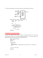
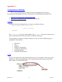
modules that can be used in a design. In the example depicted in Figure 24, a 4-bit equivalence
circuit is designed using 1-bit equivalence circuit modules.
Figure 24: Hierarchical circuit design example: 4-bit equivalence circuit
Module Definition: A module (functional block) definition is specified in a file, separate
from the top-level design file using the module.
module equiv
input p;
input q;
output r;
(p,q,r)
assign r = ~(p ^ q);
//equivalence function is xnor function.
endmodule
ptb/dkb 2013
43
EE 3320
Module Usage: A design using a module includes a declaration of module interface and
instantiation of each module in the Declaration section. Instantiation of module “equiv”
in the 4-bit equivalence circuit shown in Figure.21 can be done as follows:
module equiv4bit(a3,b3,a2,b2,a1,b1,a0,b0,eq4)
input a3,b3,a2,b2,a1,b1,a0,b0;
output eq4;
equiv eq0(a0,b0,r0);
equiv eq1(a1,b1,r1);
equiv eq2(a2,b2,r2);
equiv eq3(a3,b3,r3);
assign eq4 = r0 & r1 & r2 & r3;
endmodule
NOTE : For creation of the module, we can either use the design wizard provided by the Xilinx
or create our own.
ptb/dkb 2013
44
EE 3320
11. Post Synthesis Timing Simulation
The Xilinx ISE contains a simulator called iSIM which can be used to verify the behavior of
your designs. You may also use the Modelsim simulator which can also be invoked directly from
Xilinx in order to perform functional and timing simulations. It has an Integrated Development
environment that can be used to develop and debug Verilog synthesizable and behavioral logic.
Section 5.2 explains usage of the Modelsim simulator from Xilinx ISE to verify the functionality
of a given digital logic circuit using a test bench. This chapter deals with performing post
synthesis timing simulations using the Modelsim simulator.
We will look at simulation and timing synthesis using an example of a 4X1 multiplexer:
In order to perform the simulation, we wil need two files- a design file and a test bench (as
shown below):
The multiplexer design file (mux4x1.v):
module mux4x1 (a,b,c,d,sel,y);
input a, b, c, d;
input [1:0] sel;
output y;
reg y;
always @ (a or b or c or d or sel)
case (sel)
0 : y = a;
1 : y = b;
2 : y = c;
3 : y = d;
default : y=1'b0; //One bit binary value '0'
endcase
endmodule
A sample test bench for the multiplexer:
module mux4x1_tb ();
//output a, b, c, d;
//output [1:0] sel;
//input y;
reg a,b,c,d;
reg [1:0] sel;
initial
begin
a <= 1'b1;
b <= 1'b0;
c <= 1'b1;
d <= 1'b0;
// Wait 100 ns for global reset to finish
#100;
// Add stimulus here
sel <= 2'b00;
#200;
a<=1'b1;
b<=1'b1;
ptb/dkb 2013
45
EE 3320
sel <= 2'b01;
#400;
sel <= 2'b10;
#600;
sel <= 2'b11;
#800;
sel <= 2'b00;end
//mux4x1 mux4x1_inst(a,b,c,d,sel,y);
endmodule
As explained in the previous section, create a new project named mux4X1 and add a new verilog
source (mux4X1.v) with the code shown above.
To add a test bench select the project in the source list and right click to select ‘Add New source”
When the New source wizard pops up, select Verilog Text Fixture and choose an appropriate
name for your test bench (say, mux4X1_tb) and click on Next.
Figure 26: Creating a text fixture in Xilinx ISE
Associate your design with the test bench that you are about to create by selecting mux4x1 as the
source and click on Next and then Finish.
ptb/dkb 2013
46
EE 3320
Figure 27: Associating the testbench with the design
The tool generates a test bench with some boilerplate code as shown in Figure
Unit under test (UUT)
Code automatically generated by Xilinx
ISE. You may edit this by adding your
own test bench or modify it suitably.
Figure 28: Adding the verilog testbench to the project
ptb/dkb 2013
47
EE 3320
Double click on ‘Behavioral Check Syntax’ in the process window to make sure there are mo
syntax errors in your code. A
mark will appear if there are no errors as shown in Figure
Test stimuli added here
Syntax check successful
Figure 29: Checking syntax
Now you are ready to simulate your design!
Behavioral simulation using iSIM:
In order to run the iSIM simulator, double click on the Simulate Behavioral Model in the
process window- this will launch the iSIM window as shown in Figure 29 The output ‘y’ has
been highlighted in red for clarity.
ptb/dkb 2013
48
EE 3320
Output waveforms for
mux4x1_tb.v
Design ports
(inputs /outputs)
Figure 30: The iSIM window launched from Project Navigator
Behavioral simulation using ModelSim
You can also use ModelSim to simulate your design. To use ModelSim ensure that the Simulator
field is set to Modelsim-PE Verilog in ProjectDesign Properties (you may change it back to
iSIM if you so choose) as shown in Figure.
ptb/dkb 2013
49
EE 3320
Figure 31: Changing the simulator field in Design Properties
Double clicking on the Simulate Behavioral Model will launch the ModelSim simulator
interface.
In the Library window click on Work directory(all designs are saved in the Work directory)
choose the test bench that you want to simulate (mux4x1_tb), right click and choose ‘Simulate’.
Figure 32: The ModelSim window
ptb/dkb 2013
50
EE 3320
In the Sim window on the left, right click on the test bench name and choose ‘Add wave’
Figure 33: Adding test bench signals to the simulator
Click on Run or Run All to run the simulation.[Simulate RunRun -all]. You may choose to
run the simulation for a specified time by typing the run command in the ModelSim prompt.
ptb/dkb 2013
51
EE 3320
Run all
Simulation
Waveforms for
mux4x1_tb
Figure 34: Running the simulation and observing waveforms in ModelSim.
ptb/dkb 2013
52
EE 3320
Appendix-A:
Verilog Hardware Modeling:
This is just an introductory level tutorial to the Verilog language. The reader is
encouraged to go through the following Verilog tutorials to understand the language better:
http://www.asic-world.com/verilog/vbehave.html
http://www.vol.webnexus.com/ [requires free registration]
1. Module:
A module is the basic building block in Verilog. It is defined as follows:
module <module_name> (<portlist>);
.
.
// module components
.
endmodule
The <module_name> is the type of this module. The <portlist> is the list of connections, or
ports, which allows data to flow into and out of modules of this type.
Verilog models are made up of modules. Modules, in turn, are made of different types of
components. These include
Parameters
Nets
Registers
Primitives and Instances
Continuous Assignments
Procedural Blocks
Task/Function definitions
2. Ports:
Ports are Verilog structures that pass data between two or more modules. Thus, ports can be
thought of as wires connecting modules. The connections provided by ports can be either
input, output, or bi-directional (inout).
ptb/dkb 2013
53
EE 3320
Module instantiations also contain port lists. This is the means of connecting signals in the
parent module with signals in the child module.
3. Nets:
Nets are the things that connect model components together. They are usually thought of as wires
in a circuit. Nets are declared in statements like this:
net_type [range] [delay3] list_of_net_identifiers ;
Example:
wire w1, w2;
tri [31:0] bus32;
wire wire_number_5 = wire_number_2 & wire_number_3;
4. Registers:
Registers are storage elements. Values are stored in registers in procedural assignment
statements. Registers can be used as the source for a primitive or module instance (i.e. registers
can be connected to input ports), but they cannot be driven in the same way a net can.
Registers are declared in statements like this:
reg [range] list_of_register_identifiers ;
Example:
reg r1, r2;
reg [31:0] bus32;
ptb/dkb 2013
54
EE 3320
5. Operators in Verilog:
Logical, arithmetic and relational operators available in Verilog are described in Table 1.
Verilog Unary Operators:
Source: ASIC Design by Smith (http://www-ee.eng.hawaii.edu/~msmith/ASICs/Files/pdf/CH11.3.pdf)
Table 1 Verilog Operators
6. Continuous assignments:
Continuous assignments are sometimes known as data flow statements because they describe
how data moves from one place, either a net or register, to another. They are usually thought of
as representing combinational logic. In general, any logic functionality which can be
implemented by means of a continuous assignment can also be implemented using primitive
instances.
ptb/dkb 2013
55
EE 3320
A continuous assignment looks like this:
assign [delay3] list_of_net_assignments ;
Examples:
assign w1 = w2 & w3;
assign #1 mynet = enable; // mynet is assigned the value after 1 time unit.
7. Procedural Blocks:
Procedural blocks are the part of the language which represents sequential behavior. A module
can have as many procedural blocks as necessary. These blocks are sequences of executable
statements. The statements in each block are executed sequentially, but the blocks themselves are
concurrent and asynchronous to other blocks.
There are two types of procedural blocks, initial blocks and always blocks.
initial <statement>
always <statement>
There may be many initial and always blocks in a module. Since there may be many modules in
a model, there may be many initial and always blocks in the entire model. All initial and always
blocks contain a single statement, which may be a compound statement, e.g.
initial
begin statement1 ; statement2 ; ... end
a. Initial Block:
All initial blocks begin at time 0 and execute the initial statement. Because the statement
may be a compound statement, this may entail executing lots of statements. There may be
time or event controls, as well as all of the control constructs in the language. As a result,
an initial block may cause activity to occur throughout the entire simulation of the model.
When the initial statement finishes execution, the initial block terminates. If the initial
statement is a compound statement, then the statement finishes after its last statement
finishes.
Example:
initial x = 0; // a simple initialization
initial begin
x = 1;
y = f(x);
#1 x = 0;
y = f(x);
end
ptb/dkb 2013
// an initialization
// a value change 1 time unit later
56
EE 3320
b. Always Block:
Always blocks also begin at time 0. The only difference between an always block and an
initial block is that when the always statement finishes execution, it starts executing
again. Note that if there is no time or event control in the always block, simulation time
can never advance beyond time 0. Example,
always
#10 clock = ~clock;
8. Behavioral modeling constructs:
a. Conditional if-else construct:
The if - else statement controls the execution of other statements in a
procedural block.
Syntax:
if (condition)
statements;
if (condition)
statements;
else
statements;
if (condition)
statements;
else if (condition)
statements;
................
................
else
statements;
Example:
// Simple if statement
if (enable)
q <= d;
// One else statement
if (reset == 1'b1)
q <= 0;;
else
q <= d;
// Nested if-else-if statements
if (reset == 1'b0)
counter <= 4'b0000;
else if (enable == 1'b1 && up_en == 1'b1)
counter <= counter + 1'b1;
else if (enable == 1'b1 && down_en == 1'b1);
counter <= counter - 1'b0;
else
counter <= counter; // Redundant code
b. Case statement:
ptb/dkb 2013
57
EE 3320
The case statement compares an expression to a series of cases and executes the
statement or statement group associated with the first matching case. Case statement
supports single or multiple statements. Multiple statements can be grouped using begin
and end keywords.
Syntax:
case (<expression>)
<case1> : <statement>
<case2> : <statement>
.....
default : <statement>
endcase
Example:
module mux (a,b,c,d,sel,y);
input a, b, c, d;
input [1:0] sel;
output y;
reg y;
always @ (a or b or c or d or sel)
case (sel)
0 : y = a;
1 : y = b;
2 : y = c;
3 : y = d;
default : $display("Error in SEL");
endcase
endmodule
9. Module instantiations and hierarchies:
Verilog allows you to represent the hierarchy of a design. A more common way of depicting
hierarchical relationships is:
We say that a parent instantiates a child module. That is, it creates an instance of it to be a
submodel of the parent. In this example,
system
ptb/dkb 2013
instantiates
comp_1, comp_2
58
EE 3320
comp_2
instantiates
sub_3
Modules in a hierarchy have both a type and a name. Module types are defined in Verilog.
There can be many module instances of the same type of module in a single hierarchy. The
module definition by itself does not create a module. Modules are created by being instantiated
in another module, like this:
module <module_name_1> (<portlist>);
.
.
<module_name_2> <instance_name> (<portlist>);
.
.
endmodule
ptb/dkb 2013
59
EE 3320
Appendix-B:
This section contains some useful information on the Digilent BASYS board that will be used in
this lab. For further details please refer to the Digilent user’s manual.
B.1 Spartan 3E pin definitions
B.2 Testing the Digilent board
The Digilent Adept tool can be used to test the functionality of a BASYS board as follows:
Connect the board to the USB and set the power switch to ON.
Run Digilent Adept
Click on Test Start Test
ptb/dkb 2013
60
EE 3320
Figure B.1 The Digilent Adept test function
The tool shows you the current switch configuration and the display counts
00001111FFFF
Figure B.2 Testing the Digilent board
ptb/dkb 2013
61
EE 3320