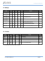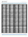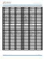
1
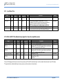
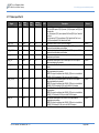
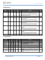
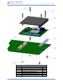
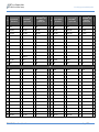
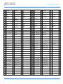
IMPT d.o.o., Belgrade, Serbia A Mihailo Pupin Institute Company Let us design your next embedded product. EPP-V7-DM8168™ Based on Texas Instruments® DaVinci™ TMS320DM8168 User Manual for hardware revision 1.0 Document revision 1.2 (December 24th, 2014) IMPT d.o.o., Belgrade, Serbia A Mihailo Pupin Institute Company Let us design your next embedded product. Preface Important Information This documentation is intended for qualified audience only. The product described herein is not an end user product. It was developed and manufactured for further processing by trained personnel. Disclaimer Although this document has been generated with the utmost care no warranty or liability for correctness or suitability for any particular purpose is implied. The information in this document is provided “as is” and is subject to change without notice. EMC Rules This unit has to be installed in a shielded housing. If not installed in a properly shielded enclosure, and used in accordance with the instruction manual, this product may cause radio interference in which case the user may be required to take adequate measures at his or her owns expense. Trademarks All used product names, logos or trademarks are property of their respective owners. EPP-V7-DM8168, User Manual, Rev. 1.2 Page 2/27 IMPT d.o.o., Belgrade, Serbia A Mihailo Pupin Institute Company Let us design your next embedded product. Content Preface ................................................................................................................................. 1 1 General Information ...................................................................................................... 4 1.1 Revision History........................................................................................................ 4 1.2 Reference Documents .............................................................................................. 4 1.3 Signal Terminology ................................................................................................... 5 1.4 Introduction............................................................................................................... 5 2 Technical Information ................................................................................................... 6 2.1 Key features(1) .......................................................................................................... 6 2.2 Jumpers and switches .............................................................................................. 7 2.3 Watchdog ................................................................................................................. 7 2.4 Power dissipation ..................................................................................................... 8 2.5 Block diagram........................................................................................................... 9 2.6 LED Indication .........................................................................................................10 2.7 Signal Description (V7 Mode) ..................................................................................10 2.7.1 2.7.2 2.7.3 2.7.4 2.7.5 2.7.6 2.7.7 2.7.8 2.7.9 2.7.10 2.7.11 2.7.12 2.7.13 2.7.14 PCI Express Lanes .......................................................................................................... 10 Ethernet ........................................................................................................................... 11 Serial ATA Interface ......................................................................................................... 12 USB Interface................................................................................................................... 12 SDIO Interface ................................................................................................................. 13 2 Audio Interface (McASP Port, I S Compatible) ............................................................... 13 HDMI Output .................................................................................................................... 14 SPI Interface .................................................................................................................... 14 Input Power Pins .............................................................................................................. 15 JTAG / UART #1 Pins (Manufacturing Signals for Qseven®-compatibility mode) .......... 15 Video Input Port 0 ............................................................................................................ 16 Video Input Port 1 ............................................................................................................ 17 Video Output Ports .......................................................................................................... 17 Power and System Management..................................................................................... 18 3 System resources ........................................................................................................19 3.1 Boot options ............................................................................................................19 3.2 I2C Bus Address Map ..............................................................................................19 4 Mechanical drawing .....................................................................................................20 5 Heat spreader ...............................................................................................................21 6 Connectors ...................................................................................................................23 6.1 MXM Connector Dimensions ...................................................................................23 6.2 MXM Connector Pin-Out..........................................................................................23 EPP-V7-DM8168, User Manual, Rev. 1.2 Page 3/27 IMPT d.o.o., Belgrade, Serbia Let us design your next embedded product. A Mihailo Pupin Institute Company 1 General Information 1.1 Revision History Rev. Date Pages 1.0 2014.07.31 All Initial version. 18 18 18 23-28 1 23-27 Updated description of V7_MODE# signal. Removed UART0_RTS# and UART0_CTS# signals. Added a notice about signal behaviour in Qseven® mode. Updated signal types for Qseven®-compatibility mode. Updated module picture. Updated pin-out table layout. 1.1 2014.10.15 1.2 2014.12.23 Description 1.2 Reference Documents [1] Qseven ® Specification 2.0 http://www.qseven-standard.org EPP-V7-DM8168, User Manual, Rev. 1.2 Page 4/27 IMPT d.o.o., Belgrade, Serbia A Mihailo Pupin Institute Company Let us design your next embedded product. 1.3 Signal Terminology Signal direction: Signal directions are from the module perspective. For example: COM_TXD (serial port transmit) is an output from the module. The “#” symbol at the end of the signal name indicates that the active or asserted state occurs when the signal is at a low voltage level. When “#” is not present, the signal is active at a high voltage level. Differential pairs are indicated by trailing “+” and “-“ signs for the positive or negative signal. 1.4 Introduction The EPP-V7-DM8168TM is part of IMPT’s Qseven®-compatible COM module family. It is based on Texas Instruments® DaVinciTM TMS320DM8168 System-on-a-Chip (SoC), incorporating a high-performance 32-bit ARM® Cortex-A8 RISC RISC MPU, 32-bit TMS320C674x floating-point VLIW DSP core, and three high-definition video codec engines based on ARM® Cortex-M3. The module is mostly compliant with the Qseven® Specification revision 2.0, in terms that it can be safely evaluated on a Qseven®-compliant carrier board (the functional difference is listed in the MXM Connector Pin-out section). However, in order to utilize the complete capabilities, including built-in video input and output ports, and both Ethernet interfaces, a special carrier board is required. IMPT offers EPP-V7-CBTM, the reference V7 carrier board for evaluation and a starting point for customizations. The EPP-V7-DM8168TM module is available in 1 or 2 GBytes of DDR3 memory variants, in both industrial and commercial temperature range. EPP-V7-DM8168, User Manual, Rev. 1.2 Page 5/27 IMPT d.o.o., Belgrade, Serbia Let us design your next embedded product. A Mihailo Pupin Institute Company 2 Technical Information 2.1 Key features(1) CPU ARM® Cortex-A8 RISC processor operating at 1.2 GHz 32KB instruction and data caches 256KB L2 cache 64KB RAM, 48KB boot ROM C674x floating/fixed point DSP operating at 1 GHz Up to 8000/6000 C674x MIPS/MFLOPS Memory Dual 32-bit DDR3 SDRAM at 800 MHz (1600 MT/s), 1 or 2 GBytes HD Video Processors Three HDVICP2 Cortex-M3 based hardware engines supporting encoding & decoding video in resolutions up to 1080p60. Video outputs Video inputs GPU MPEG1, MPEG2, MPEG4 (ASP and SP) H.264 (BL, MP and HP) VC-1 (SP, MP and AP) RV9 and RV10 AVS 1.0 ON2 (VP6.2 and VP7) One digital HDMI 1.3 transmitter with HDCP, up to 1080p60 One 16-bit paralel video output port (supporting YCbCr and BT.656 modes up to 165 MHz) with separate HSync/VSync signals, allowing embedded and discrete sync modes One SD analog output with separate Y/C channels, compatible with S-video standard One 24-bit paralel video input port (up to 165 MHz) with separate HSync/VSync signals, supporting single-channel 16-bit/24-bit (YCbCr and RGB) video with embedded or discrete sync, or dual-channel 8-bit (YCbCr) with embedded sync One 16-bit paralel video input port (up to 165 MHz) with separate HSync/VSync signals, supporting single-channel 16-bit (YCbCr) video with embedded or discrete(2) sync, or dual-channel 8-bit (YCbCr) video with embedded sync SGX530 3D Graphics Engine Delivers up to 30 MTriangles/s Compatible with OpenGL ES 1.1/2.0 and OpenVG v1.1 Ethernet Dual Micrel KSZ9031MNX Ethernet PHY, IEEE 802.3 compliant (full duplex 10Base-T/100Base-TX/1000Base-T) PCI Express One PCI Express Gen2 dual-lane port EPP-V7-DM8168, User Manual, Rev. 1.2 Page 6/27 IMPT d.o.o., Belgrade, Serbia Let us design your next embedded product. A Mihailo Pupin Institute Company Audio One Texas Instruments McASP port, I2S-compatible(3) USB Dual USB 2.0 Controller (supports host and client modes) SATA Dual SATA 3.0 Gbps interface Serial, SPI, I2C Flash Memory Two UART ports (one with RTS/CTS flow control, one supporting TX/RX only and multiplexed with JTAG port) SPI controller up to 40 MHz (two chip selects available on the connector) Two I2C ports supporting 100 kHz and 400 kHz modes 8-bit NAND Flash, 2 GByte capacity SPI Flash, 4 MB capacity SDIO 4-bit SD/MMC Controller supporting 2.00 specification (HighSpeed), up to 48 MHz RTC RTC via I2C-Interface (typical power consumption 350 nA @ 3V) Temperature sensor Connected to the power management module Boot sources(4) SD card SPI Flash Package 1031-Pin Pb-Free BGA Package, 25,2x25,2mm, 0,65mm pitch, 2,81mm max. height. Power Supply 5V (4,75V – 5,25V) 5V (4,75V – 5,25V) standby voltage 3V (1,3V – 3,3V) optionally for RTC 1 Features listed in this table are fully available only in V7 mode. Features disabled in Qseven®compatibility mode are listed in a separate table. 2 Due to pin multiplexing in the chip, HSync/VSync pins for the second (16-bit) video input port are shared with data signals in the upper octet of the first (24-bit) input port. If the first port is used in full 24-bit mode, discrete sync is not available for the second port. 3 It is highly recommended to use McASP compatible audio codecs (such as TLV320AIC310x family) on the carrier board, due to better software support in Linux operating system. 4 U-Boot bootloader must be installed in onboard SPI Flash or the SD Card. When U-Boot is loaded and executed, main operating system can be loaded over Ethernet. 2.2 Jumpers and switches There are no jumpers or switches available on the module. 2.3 Watchdog External watchdog is not supported in current software distribution, since DM8168 has a built-in watchdog. EPP-V7-DM8168, User Manual, Rev. 1.2 Page 7/27 IMPT d.o.o., Belgrade, Serbia Let us design your next embedded product. A Mihailo Pupin Institute Company 2.4 Power dissipation Mode Voltage Current Power Description Idle 5V TBD TBD Measured at the login prompt ten minutes after booting CPU tests 5V TBD TBD Measured while running CPU tests fifteen minutes after booting HD video 5V TBD TBD Measured while decoding HD video (hardware accelerated) two minutes after rebooting EPP-V7-DM8168, User Manual, Rev. 1.2 Page 8/27 IMPT d.o.o., Belgrade, Serbia Let us design your next embedded product. A Mihailo Pupin Institute Company 2.5 Block diagram TI DaVinci DM8168 2 x SATA 3.0 Gpbs PCI Express Gen2 dual-lane C674x DSP HD Video Encoding Engines 3D Graphics Engine HD Video Capture / Display Engine McASP port HDMI 24-bit VIN0 16-bit VOUT0 16-bit VOUT0 SPI (three CS) SPI (two CS) DDR3 MEMORY INTERFACE SPI Flash CPLD MXM Edge Connector DDR3-1600 1 or 2 Gbyte 16-bit VIN1 UART #1 GENERAL MEMORY INTERFACE ARM Cortex A8 Manufacturing Signals (0-4) JTAG NAND Flash 2 Gbyte JTAG 2 x I2C 2 x USB 2.0 SD card (4-bit) UART #2 Power Management Unit UART #0 I2C I2C Temp. sensor RTC Analog Y/C VOUT Analog video amp. Analog Y/C VOUT GMII Gigabit Ethernet PHY Gigabit Ethernet GMII Gigabit Ethernet PHY Gigabit Ethernet RTC Backup Supply EPP-V7-DM8168 EPP-V7-DM8168, User Manual, Rev. 1.2 Version 1.0 Page 9/27 IMPT d.o.o., Belgrade, Serbia Let us design your next embedded product. A Mihailo Pupin Institute Company 2.6 LED Indication There are three onboard LEDs controllable by software and available for user application. However, in normal operation they are covered by heatsink and are not visible from the outside. Please consult the BSP manual for instructions how to control them in Linux operating system. 2.7 Signal Description (V7 Mode) In the following table, signals are marked with the power rail associated with the pin, and with the input voltage tolerance (for input and I/O pins). The pin power rail and the pin input voltage tolerance maybe different. 2.7.1 PCI Express Lanes Pin Type PCIE0_TX+ PCIE0_TXPCIE0_RX+ PCIE0_RX- O Signal Level PCIe I PCIe CPU PCIE1_TX+ PCIE1_TXPCIE1_RX+ PCIE1_RX- O PCIe CPU I PCIe CPU PCIE_CLK_REF+ PCIE_CLK_REF- O PCIe CPU PCIE_RST# PCIE_WAKE# O I CMOS CMOS CPU CPU Signal Power Rail CPU EPP-V7-DM8168, User Manual, Rev. 1.2 Remark / Power Tol. AC coupled on module Requires AC coupling on baseboard AC coupled on module Requires AC coupling on baseboard AC coupled on module 3.3V 3.3V PU/PD Description Source PCI Express Gen2 differential transmit pairs 0. DM8168 PCI Express Gen2 differential receive pairs 0. Exp. connector PCI Express Gen2 differential transmit pairs 1. DM8168 PCI Express Gen2 differential receive pairs 1. Exp. connector PCI Express reference clock. Onboard clock generator Reset signal output. External wake signal input. DM8168 Exp. connector Page 10/27 IMPT d.o.o., Belgrade, Serbia Let us design your next embedded product. A Mihailo Pupin Institute Company 2.7.2 Ethernet Signal GBE0_MDI[0:3]+ GBE0_MDI[0:3]GBE1_MDI[0:3]+ GBE1_MDI[0:3]+ Pin Type I/O Signal Level Ethernet MDI Power Rail Remark / Power Tol. CPU PU/PD Description Source Gigabit Ethernet Controller: Media Dependent Interface Differential Pairs 0, 1, 2, and 3. The MDI can operate in 1000Base-T, 100Base-TX and 10Base-T modes. Ethernet PHY 1000BASE-T MDI configuration: MDI[0]+/MDI[1]+/MDI[2]+/MDI[3]+/- BI_DA+/BI_DB+/BI_DC+/BI_DD+/- MDI-X configuration: MDI[0]+/MDI[1]+/MDI[2]+/MDI[3]+/- BI_DB+/BI_DA+/BI_DC+/BI_DD+/- 100BASE-TX/ 10BASE-T MDI configuration: MDI[0]+/MDI[1]+/MDI[2]+/MDI[3]+/- GBE0_ACT# GBE1_ACT# GBE0_LINK# GBE1_LINK# GBE0_LINK100# GBE1_LINK100# GBE0_LINK1000# GBE1_LINK1000# GBE0_CTREF GBE1_CTREF Transmit Receive unused unused MDI-X configuration: MDI[0]+/MDI[1]+/MDI[2]+/MDI[3]+/- Receive Transmit unused unused O CMOS CPU 3.3V Gigabit Ethernet Controller: activity indicator, active low. Eth PHY O CMOS CPU 3.3V Gigabit Ethernet Controller: link indicator, active low. Eth PHY O CMOS CPU 3.3V Gigabit Ethernet Controller: 100 Mbit mode indicator, active low. DM8168 O CMOS CPU 3.3V Gigabit Ethernet Controller: 1000 Mbit mode indicator, active low. DM8168 GND min 3.3V max Gigabit Ethernet Controller: unconnected Not connected NC EPP-V7-DM8168, User Manual, Rev. 1.2 Page 11/27 IMPT d.o.o., Belgrade, Serbia Let us design your next embedded product. A Mihailo Pupin Institute Company 2.7.3 Serial ATA Interface Signal SATA0_TX+ SATA0_TXSATA0_RX+ SATA0_RXSATA1_TX+ SATA1_TXSATA1_RX+ SATA1_RXSATA_ACT# 2.7.4 Pin Type O Signal Level SATA CPU I SATA CPU O SATA CPU I SATA CPU OD Output CMOS CPU Power Rail Remark / Power Tol. AC coupled on module AC coupled on module AC coupled on module AC coupled on module 3.3V PU/PD Description Source Serial ATA Channel 0: differential transmit pair. DM8168 Serial ATA Channel 0: differential receive pair. Exp. connector Serial ATA Channel 1: differential transmit pair. DM8168 Serial ATA Channel 1: differential receive pair. Exp. connector SATA activity indicator (mutual for both channels), active low. An external pull-up needs to be installed on the carrier board. DM8168 USB Interface Pin Type I/O Signal Level USB CPU USB differential pair, channels 0. I/O USB CPU USB differential pair, channels 1. I CMOS CPU 3.3V USB_ID I CMOS CPU 3.3V USB_CC I CMOS CPU 3.3V Signal USB_P0+ USB_P0USB_P1+ USB_P1USB_0_1_OC# Power Rail EPP-V7-DM8168, User Manual, Rev. 1.2 Remark / Power Tol. PU/PD 1k43 PU Description USB over-current sense for both USB channels. A pull-up for this line is present on the module. An open drain driver from a USB current monitor on the carrier board may drive this line low. Do not pull this line high on the carrier board. USB ID pin. High signal level can be used in software to configure USB Port 0 or 1 as USB client. USB client connect pin. Source DM8168 or exp. connector DM8168 or exp. connector Exp. connector Exp. connector Exp. connector Page 12/27 IMPT d.o.o., Belgrade, Serbia Let us design your next embedded product. A Mihailo Pupin Institute Company 2.7.5 SDIO Interface SDIO_DAT[0:3] I/O Signal Level 3.3V SDIO_CD# I 3.3V CPU 3.3V SDIO_CMD I/O 3.3V CPU 3.3V 10k PU SDIO command line. SDIO_CLK SDIO_PWR# O I/O 3.3V 3.3V CPU CPU 3.3V 3.3V 10k PU 10k PU SDIO clock line. SDIO power enable signal. SDIO_LED SDIO_WP O I 3.3V 3.3V CPU CPU 3.3V 3.3V 10k PD SDIO transfer activity LED. SDIO write protect signal. Signal Pin Type CPU Remark / Power Tol. 3.3V Power Rail PU/PD 10k PU Description Source SDIO data lines. DM8168 or exp. connect. Exp. connector DM8168 or exp. connect. DM8168 DM8168 or exp. connect. DM8168 Exp. connector SDIO card detect signal. 2.7.6 Audio Interface (McASP Port, I2S Compatible) Signal I2S_RST# I2S_WS / MCA2_AFSX I2S_CLK / MCA2_ACLKX I2S_SDO / MCA2_AXR1 I2S_SDI / MCA2_AXR0 MCA2_AHCLKX Output Output Signal Level CMOS CMOS CPU CPU Remark / Power Tol. 3.3V 3.3V Output CMOS CPU Output CMOS Input I/O Pin Type Power Rail PU/PD Description Source Reset output to carrier board’s audio codec, active low. I2S word select clock to codec (WCLK for codecs with McASP interface). DM8168 DM8168 3.3V I2S bit clock to codec (BCLK for codecs with McASP interface). DM8168 CPU 3.3V Serial data output to codec. DM8168 CMOS CPU 3.3V Serial data input from codec. CMOS CPU 3.3V MCLK for codecs with McASP interface. Exp. connector DM8168 or exp. connect. EPP-V7-DM8168, User Manual, Rev. 1.2 10k PD Page 13/27 IMPT d.o.o., Belgrade, Serbia Let us design your next embedded product. A Mihailo Pupin Institute Company 2.7.7 HDMI Output DP_LANE2+/TMDS_LANE0+ DP_LANE2-/TMDS_LANE0DP_LANE1+/TMDS_LANE1+ DP_LANE1-/TMDS_LANE1DP_LANE0+/TMDS_LANE2+ DP_LANE0-/TMDS_LANE2DP_LANE3+/TMDS_CLK+ DP_LANE3-/TMDS_CLKDP_HDMI_HPD# O Signal Level HDMI O HDMI O Signal Pin Type Power Rail CPU Remark / Power Tol. PU/PD Description Source TMDS differential pair lines, lane 0. DM8168 CPU TMDS differential pair lines, lane 1. DM8168 HDMI CPU TMDS differential pair lines, lane 2. DM8168 O HDMI CPU TMDS differential pair lines, clock. DM8168 I CMOS CPU Exp. connector HDMI_CTRL_CLK I/O OD CMOS CPU 3.3V 40k2 PU Hot-plug detection signal that serves as an interrupt request line. Signal can be pulled only to a logic low level. DDC based control signal (clock) for HDMI device. HDMI_CTRL_DAT I/O OD CMOS CPU 3.3V 40k2 PU DDC based control signal (data) for HDMI device. DM8168 2.7.8 DM8168 SPI Interface SPI_MOSI SPI_MISO SPI_SCK SPI_CS0# Pin Type O I O O Signal Level CMOS CMOS CMOS CMOS SPI_CS1# O CMOS Signal 1 10k PD CPU CPU CPU CPU Remark / Power Tol. 3.3V 3.3V 3.3V 3.3V 5k1 PU Master serial output. Master serial input / Peripheral serial output. SPI clock output. (1) The second SPI chip select output, active low. CPU 3.3V 5k1 PU The third Power Rail PU/PD Description (1) SPI chip select output, active low. Source DM8168 Exp. connector DM8168 DM8168 DM8168 First SPI chip select signal is reserved for access to onboard SPI Flash memory. EPP-V7-DM8168, User Manual, Rev. 1.2 Page 14/27 IMPT d.o.o., Belgrade, Serbia Let us design your next embedded product. A Mihailo Pupin Institute Company 2.7.9 Input Power Pins VCC Pin Type Power VCC_5V0_SB Power 5V VCC_RTC GND Power Power Suspend Signal Signal Level Power Rail 5V Remark / Power Tol. (±5%) (±5%) PU/PD Description Source Primary power input towards voltage regulators: +5V (±5%). Exp. connector Standby power input towards voltage regulators: +5.0V (±5%) All available VCC5V0_STBY pins on the connector(s) shall be used. Used for microcontroller and standby and suspend functions. NOTE: If no standby power is available, connect it to VCC5V0! Real-time clock circuit-power input : +3.0V (+1.3V to +3.3V). Ground - DC power and signal and AC signal return path. All available GND connector pins shall be used and tied to Carrier Board GND plane. Exp. connector Exp. connector 2.7.10 JTAG / UART #1 Pins (Manufacturing Signals for Qseven®-compatibility mode) Pin Type MFG_NC0 / JTAG_TCLK MFG_NC1 / JTAG_TDO / UART1_TX I O Signal Level CMOS CMOS MFG_NC2 / JTAG_TDI / UART1_RX I CMOS CPU 3.3V MFG_NC3 / JTAG_TMS (3) MFG_NC4 / JTAG_TRST# / MFG_SEL I I CMOS CMOS CPU CPU 3.3V 3.3V Signal (2) Power Rail CPU CPU Remark / Power Tol. 3.3V 3.3V PU/PD Description Boundary Scan – TCK Boundary Scan – TDO / COM_TXD: Depending on MFG_NC4 level, the signal is either used as Boundary Scan TDO, or as transmit line for UART #1 port. Boundary Scan – TDI / COM_RXD: Depending on MFG_NC4 level, the signal is either used as Boundary Scan TDI, or as receive line for UART #1 port. Boundary Scan – TMS. Control Signal for multiplexer circuit: 1: Boundary Scan / JTAG 0: UART #1 Source Exp. connector DM8168 Exp. connector Exp. connector Exp. connector 2 On some JTAG debuggers which require a return clock from processor, pins TCK and RCK should be tied (pins 11 and 9 on standard Texas Instruments 14-pin JTAG Header). 3 This signal should have a defined default logic level (using a pull-up or pull-down resistor on the carrier board). EPP-V7-DM8168, User Manual, Rev. 1.2 Page 15/27 IMPT d.o.o., Belgrade, Serbia Let us design your next embedded product. A Mihailo Pupin Institute Company 2.7.11 Video Input Port 0 Pin Type VIN[0]A_D[0:23] I Signal Level CMOS VIN[0]A_CLK VIN[0]A_HSYNC I I CMOS CMOS CPU CPU 3.3V 3.3V VIN[0]A_VSYNC I CMOS CPU 3.3V VIN[0]A_FLD I CMOS CPU 3.3V VIN[0]A_DE I CMOS CPU 3.3V VIN[0]B_CLK I CMOS CPU 3.3V VIN[0]B_HSYNC I CMOS CPU 3.3V VIN[0]B_VSYNC I CMOS CPU 3.3V VIN[0]B_FLD I CMOS CPU 3.3V VIN[0]B_DE I CMOS CPU 3.3V Signal Power Rail CPU Remark / Power Tol. 3.3V EPP-V7-DM8168, User Manual, Rev. 1.2 PU/PD Description Digital VIN0 port data lines. For 24-bit RGB capture, D[23:16] are red, D[15:8] are green, and D[7:0] are blue data bits. For 16-bit capture, D[7:0] are multiplexed Cb/Cr and D[15:8] are Y data bits for Port A. For 8-bit capture, D[7:0] are multiplexed YCbCr data bits for Port A, and D[15:8] are multiplexed YCbCr data bits for Port B. Input clock for 8-bit, 16-bit, or 24-bit Port A capture. Discrete horizontal synchronization signal for Port A RGB capture, or YCbCr capture without embedded synchronization. Discrete vertical synchronization signal for Port A RGB capture, or YCbCr capture without embedded synchronization. Discrete field ID signal for Port A RGB capture, or YCbCr capture without embedded synchronization. Discrete data enable signal for Port A RGB capture, or YCbCr capture without embedded synchronization. Input clock for 8-bit Port B capture. Not used in 16-bit and 24-bit capture modes. Discrete horizontal synchronization signal for Port B 8-bit YCbCr capture without embedded synchronization. NOTE: This signal is multiplexed with VIN[0]A_D[23] and is not available for VIN[0]B_HSYNC functionality if VIN0 port is used for 24-bit capture. Discrete vertical synchronization signal for Port B 8-bit YCbCr capture without embedded synchronization. NOTE: This signal is multiplexed with VIN[0]A_D[22] and is not available for VIN[0]B_VSYNC functionality if VIN0 port is used for 24-bit capture. Discrete field ID signal for Port B 8-bit YCbCr capture without embedded synchronization. NOTE: This signal is multiplexed with VIN[0]A_D[21] and is not available for VIN[0]B_FLD functionality if VIN0 port is used for 24-bit capture. Discrete data enable signal for Port B 8-bit YCbCr capture without embedded synchronization. NOTE: This signal is multiplexed with VIN[0]A_D[20] and is not available for VIN[0]B_DE functionality if VIN0 port is used for 24-bit capture. Source Exp. conn. Exp. conn. Exp. conn. Exp. conn. Exp. conn. Exp. conn. Exp. conn. Exp. conn. Exp. conn. Exp. conn. Exp. conn. Page 16/27 IMPT d.o.o., Belgrade, Serbia Let us design your next embedded product. A Mihailo Pupin Institute Company 2.7.12 Video Input Port 1 Pin Type VIN[1]A_D[0:15] I Signal Level CMOS VIN[1]A_CLK VIN[1]A_HSYNC I I CMOS CMOS CPU CPU 3.3V 3.3V VIN[1]A_VSYNC I CMOS CPU 3.3V VIN[1]A_FLD I CMOS CPU 3.3V VIN[1]A_DE I CMOS CPU 3.3V VIN[1]B_CLK I CMOS CPU 3.3V Signal Power Rail CPU Remark / Power Tol. 3.3V PU/PD Description Source Digital VIN1 port data lines. For 16-bit capture, D[7:0] are Cb/Cr and D[15:8] are Y data bits for Port A. For 8-bit capture, D[7:0] are multiplexed YCbCr data bits for Port A, and D[15:8] are multiplexed YCbCr data bits for Port B. Input clock for 8-bit or 16-bit Port A capture. Discrete horizontal synchronization signal for Port A YCbCr capture without embedded synchronization. NOTE: This signal is multiplexed with VIN[0]A_D[16] and is not available for VIN[1]A_HSYNC functionality if VIN0 port is used for 16-bit or 24-bit capture. Discrete vertical synchronization signal for Port A YCbCr capture without embedded synchronization. NOTE: This signal is multiplexed with VIN[0]A_D[17] and is not available for VIN[1]A_VSYNC functionality if VIN0 port is used for 16-bit or 24-bit capture. Discrete field ID signal for Port A YCbCr capture without embedded synchronization. NOTE: This signal is multiplexed with VIN[0]A_D[18] and is not available for VIN[1]A_FLD functionality if VIN0 port is used for 16-bit or 24-bit capture. Discrete data enable signal for for Port A YCbCr capture without embedded synchronization. NOTE: This signal is multiplexed with VIN[0]A_D[19] and is not available for VIN[1]A_DE functionality if VIN0 port is used for 16-bit or 24-bit capture. Input clock for 8-bit Port B video capture. Not used in 16-bit capture mode. Exp. conn. Exp. conn. Exp. conn. Exp. conn. Exp. conn. Exp. conn. Exp. conn. 2.7.13 Video Output Ports VDAC_Y VDAC_C VOUT[0]_CLK VOUT[0]_FLD VOUT[0]_HSYNC VOUT[0]_VSYNC VOUT[0]_G_Y_YC[2:9] Pin Type O O O O O O O Signal Level S-Video S-Video CMOS CMOS CMOS CMOS CMOS Power Rail CPU CPU CPU CPU CPU CPU CPU 3.3V 3.3V 3.3V 3.3V 3.3V VOUT[0]_B_CB_C[2:9] O CMOS CPU 3.3V Signal EPP-V7-DM8168, User Manual, Rev. 1.2 Remark / Power Tol. PU/PD PD, 37.4O PD, 37.4O Description Source Luma (Y) component of the analog SD video output port. Chroma (C) component of the analog SD video output port. Digital VOUT0 port, output clock. Digital VOUT0 port, discrete field ID output signal. Discrete horizontal synchronization signal (not used for embedded sync modes). Discrete vertical synchronization signal (not used for embedded sync modes). Y (Luma) data bits for 16-bit YCbCr mode; Multiplexed YCbCr data bits for 8-bit BT.656 mode. Multiplexed CbCr (Chroma) data bits for 16-bit YCbCr mode; Unused for 8-bit BT.656 mode. Video amp. Video amp. CPLD CPLD CPLD CPLD CPLD CPLD Page 17/27 IMPT d.o.o., Belgrade, Serbia Let us design your next embedded product. A Mihailo Pupin Institute Company 2.7.14 Power and System Management Signal V7_MODE# Pin Type Power (N/C) Signal Level Power Rail 5V Remark / Power Tol. 5V 10k PU PU/PD PWRBTN# RSTBTN# I I CMOS CMOS Suspend Suspend 3.3V 3.3V 10k PU 10k PU SUS_S3# O CMOS Suspend 3.3V 10k PD WAKE# PWGIN GP0_I2C_CLK GP0_I2C_DAT GP1_I2C_CLK GP1_I2C_DAT EXT_INT1# EXT_INT2# UART0_TX UART0_RX I I I/O I/O I/O I/O I I O I CMOS 5V CMOS CMOS CMOS CMOS CMOS CMOS CMOS CMOS CMOS Suspend Suspend CPU CPU CPU CPU CPU CPU CPU CPU 3.3V 5V 3.3V 3.3V 3.3V 3.3V 3.3V 3.3V 3.3V 3.3V 10k PU 1k43 PU 1k43 PU 5k1 PU 5k1 PU 10k PU Description Source Carrier board detection signal. Used by the power management subsystem to detect carrier board type and automatically reconfigure the connector pin-out between V7 mode and Qseven®-compatibility mode. This signal is connected to 5V power rail on Qseven® carrier boards, but it must be left disconnected on V7-compliant carrier boards (otherwise, wrong carrier board detection will occur, which can damage the hardware). Power button to bring system into a power state. Active low (negative pulse). Reset button input. System is held in hardware reset while this input is low, and comes out of reset upon release. Active low (negative pulse). Power management output which is used to switch the main power supply. Active low. External system wake up signal. Active low. Indicates that the external power supply is ready. General purpose I2C port 0 clock output. General purpose I2C port 0 data line. General purpose I2C port 1 clock output. General purpose I2C port 1 clock output. General purpose external interrupt source. Active low. General purpose external interrupt source. Active low. Transmit line for UART #0 port. Receive line for UART #0 port. Exp. connector (leave N/C on V7-compliant carrier boards) Exp. connector Exp. connector Power mgmnt. unit Exp. connector Exp. connector DM8168 DM8168 DM8168 DM8168 Exp. connector Exp. connector DM8168 Exp. connector NOTE: Please examine the pin-out difference between V7 mode and Qseven®-compatibility mode (listed in a separate section of this document), and also refer to Qseven® specification 2.0, which contains the exact description and nature of signals not listed in V7 signal description tables. EPP-V7-DM8168, User Manual, Rev. 1.2 Page 18/27 IMPT d.o.o., Belgrade, Serbia Let us design your next embedded product. A Mihailo Pupin Institute Company 3 System resources 3.1 Boot options The EPP-V7-DM8168TM supports multiple booting options. The bootloader (“UBoot”) can be loaded from SD card or the onboard SPI Flash memory. SD card boot is of higher priority than SPI Flash boot, which is useful for development and as a rescue method (when data on SPI Flash gets corrupted or accidentally overwritten). If an SD card is present in the system, but doesn't contain a valid bootloader, the CPU will skip to SPI Flash boot method. When the U-Boot bootloader is loaded and started, Linux operating system can be loaded via Ethernet, NAND Flash, or SD Card. Please consult the Linux BSP manual for complete information about boot options. 3.2 I2C Bus Address Map The following addresses are in use by I2C peripherals on the module, and should not be used for peripherals on the carrier board. Device on I2C A6 Module Bus A5 A4 A3 A2 A1 A0 R/ W Address (8-bit RW) Adress in Linux PMIC 0 0 1 0 1 1 0 1 x 5Ah / 5Bh 2Dh RTC 0 1 1 0 1 0 0 0 x D0h / D1h 68h NOTES: In default software configuration shipped with the module, audio codec on the carrier board (such as EPP-V7-CBTM) is expected to have the address 18h on I2C bus 0 (not counting r/w bit, which is automatically set by the operating system depending on read or write request). Multiple video capture and display controllers, and the controlling GPIO I2C expander, are expected at several addresses on I2C bus 1 when running default software configuration on the reference V7 carrier board (EPP-V7-CBTM). Please consult the user manual for EPP-V7-CBTM for the list of exact addresses. EPP-V7-DM8168, User Manual, Rev. 1.2 Page 19/27 IMPT d.o.o., Belgrade, Serbia A Mihailo Pupin Institute Company Let us design your next embedded product. 4 Mechanical drawing The actual height depends on the MXM connector used on the baseboard. EPP-V7-DM8168, User Manual, Rev. 1.2 Page 20/27 IMPT d.o.o., Belgrade, Serbia A Mihailo Pupin Institute Company 5 Let us design your next embedded product. Heat spreader The EPP-V7-DM8168TM module uses a cooling solution for Qseven® module, which is based on a heat spreader concept. The purpose of the heat spreader is to provide a standard thermal interface. A heat spreader is a metal plate (typically aluminium) mounted on top of the module. Its mechanical dimensions follow the module standard specification. The connection between the metal plate and the thermal active components on the module is typically made via thermal interface materials such as phase change foils, gap pads and metal blocks. A good thermal conductivity is required in order to transfer the heat from the hotspots to the heat spreader plate. The heat spreader used for the EPP-V7-DM8168TM module is thermally attached using phase change materials and a small aluminium block that is part of the heat spreader plate. Usage of the heat spreader is obligatory, but there might be applications that require additional type of cooling solution together with heat spreader (passive casing heat dissipation or cooling fan). In any case, it is the system designer’s responsibility to make sure that each device in the system operates within its specified thermal limits. The cooling solution should ensure that the thermal specifications for each component are met over the full operating range of the system. EPP-V7-DM8168, User Manual, Rev. 1.2 Page 21/27 IMPT d.o.o., Belgrade, Serbia Let us design your next embedded product. A Mihailo Pupin Institute Company Bill of Material Pos-Nr. 1 2 3 4 5 6 7 8 Description Qty TM EPP-V7-DM8168 HSP-001 Qseven® or V7 carrier board TM EPP-V7-DM8168 MEC Q7 COOLSTRIP ALU 70x5x5 MEC BOLT HEX-M/F M2.5 SW4 L5 MEC Screw Fillister Head M2.5x20 Cross MEC Screw Fillister Head M2.5x6 Cross MEC NUT HEX M2.5 SW5 m2.0 EPP-V7-DM8168, User Manual, Rev. 1.2 1 1 1 1 2 2 2 2 Page 22/27 IMPT d.o.o., Belgrade, Serbia A Mihailo Pupin Institute Company Let us design your next embedded product. 6 Connectors 6.1 MXM Connector Dimensions 6.2 MXM Connector Pin-Out The following table shows the comparison between Qseven® pinout and both pinout modes supported by the EPP-V7-DM8168TM module (V7 mode and Qseven®-compatible mode). The pinout is automatically reconfigured depending on the type of carrier board in which the module is working. Legend: IO: Input/output; I: Input; O: Output; L: Output driven low; PD: Internal pull-down active; PU: Internal pull-up active; OD: Open drain; Z: High-Z; P: Power; NA: Not available (reserved). EPP-V7-DM8168, User Manual, Rev. 1.2 Page 23/27 IMPT d.o.o., Belgrade, Serbia Let us design your next embedded product. A Mihailo Pupin Institute Company GND P GND P 2 GND P GND P GND P IO GBE0_MDI3- IO GBE_MDI3- IO 4 GBE_MDI2- IO GBE0_MDI2- IO GBE_MDI2- IO 5 GBE_MDI3+ IO GBE0_MDI3+ IO GBE_MDI3+ IO 6 GBE_MDI2+ IO GBE0_MDI2+ IO GBE_MDI2+ IO 7 GBE_LINK100# O GBE0_LINK100# O GBE_LINK100# O 8 GBE_LINK1000# O GBE0_LINK1000# O GBE_LINK1000# O 9 GBE_MDI1- IO GBE0_MDI1- IO GBE_MDI1- IO 10 GBE_MDI0- IO GBE0_MDI0- IO GBE_MDI0- IO 11 GBE_MDI1+ IO GBE0_MDI1+ IO GBE_MDI1+ IO 12 GBE_MDI0+ IO GBE0_MDI0+ IO GBE_MDI0+ IO 13 GBE_LINK# O GBE0_LINK# O GBE_LINK# O 14 GBE_ACT# O GBE0_ACT# O GBE_ACT# 15 GBE_CTREF P GBE0_CTREF P GBE_CTREF P 16 SUS_S5# O VIN[0]A_D[20] / VIN[0]B_DE I N/A 17 WAKE# I WAKE# I WAKE# I 18 SUS_S3# O SUS_S3# O SUS_S3# O I N/A PU 20 PWRBTN# I PWRBTN# I PWRBTN# I O N/A Z 22 LID_BTN# I VDAC_C O N/A Z P 24 GND P GND P GND P I PWGIN I PWGIN I 19 SUS_STAT# O VIN[0]A_D[21] / VIN[0]B_FLD 21 SLP_BTN# I VDAC_Y 23 GND P GND P GND TM EPP-V7-DM8168 signal in V7 mode Type Type P GBE_MDI3- Signal in Qseven® specification 2.0 Type GND 3 TM EPP-V7-DM8168 signal in V7 mode Type 1 Type EPP-V7-DM8168 signal in Qseven®compatibility mode Signal in Qseven® specification 2.0 EPP-V7-DM8168 signal in Qseven®compatibility mode TM Type TM Pin Pin O PU KEY 25 GND P 26 PWGIN 27 29 BATLOW# I 28 RSTBTN# I RSTBTN# I RSTBTN# I SATA0_TX+ O 30 SATA1_TX+ O SATA1_TX+ O SATA1_TX+ O O SATA0_TX- O 32 SATA1_TX- O SATA1_TX- O SATA1_TX- O SATA_ACT# OD SATA_ACT# OD 34 GND P GND P GND P SATA0_RX+ I SATA0_RX+ I 36 SATA1_RX+ I SATA1_RX+ I SATA1_RX+ I I SATA0_RX- I SATA0_RX- I 38 SATA1_RX- I SATA1_RX- I SATA1_RX- I GND P GND P GND P 40 GND P GND P GND P BIOS_DISABLE# I GBE1_ACT# O BIOS_DISABLE# I 42 SDIO_CLK# O SDIO_CLK# O SDIO_CLK# O IO SDIO_CD# IO SDIO_CD# IO 44 SDIO_LED O SDIO_LED O SDIO_LED O SDIO_CMD IO SDIO_CMD IO SDIO_CMD IO 46 SDIO_WP IO SDIO_WP IO SDIO_WP IO SDIO_PWR# O SDIO_PWR# O SDIO_PWR# O 48 SDIO_DAT1 IO SDIO_DAT1 IO SDIO_DAT1 IO 49 SDIO_DAT0 IO SDIO_DAT0 IO SDIO_DAT0 IO 50 SDIO_DAT3 IO SDIO_DAT3 IO SDIO_DAT3 IO 51 SDIO_DAT2 IO SDIO_DAT2 IO SDIO_DAT2 IO 52 SDIO_DAT5 IO GBE1_CTREF P N/A Z 53 SDIO_DAT4 IO GBE1_MDI3- IO N/A I 54 SDIO_DAT7 IO GBE1_MDI2- IO N/A I P GND P GND BATLOW# I SATA0_TX+ O EXT_INT2# I SATA0_TX+ O 31 SATA0_TX- O SATA0_TX- 33 35 SATA_ACT# OD SATA0_RX+ I 37 SATA0_RX- 39 41 43 SDIO_CD# 45 47 EPP-V7-DM8168, User Manual, Rev. 1.2 Page 24/27 IMPT d.o.o., Belgrade, Serbia Let us design your next embedded product. A Mihailo Pupin Institute Company 55 SDIO_DAT6 IO GBE1_MDI3+ IO N/A I 56 RSVD NA 57 GND P GND P GND P 58 GND P 59 I2S_WS O I2S_WS/ MCA[2]_AFSX O I2S_WS O 60 SMB_CLK /GP1_I2C_CLK OD GP0_I2C_CLK OD GP0_I2C_CLK OD OD GP0_I2C_DAT OD GP0_I2C_DAT OD 61 I2S_RST# N/A I P GND P O I2S_RST# O I2S_RST# O 62 O I2S_CLK O 64 SMB_ALERT# OD EXT_INT1# OD SMB_ALERT# OD I I2S_SDI I 66 GP0_I2C_CLK OD GP1_I2C_CLK OD GP1_I2C_CLK OD O I2S_SDO O 68 GP0_I2C_DAT OD GP1_I2C_DAT OD GP1_I2C_DAT OD 63 I2S_CLK O 65 I2S_SDI I I2S_SDI/ MCA[2]_AXR[0] I2S_SDO IO GND SMB_DAT /GP1_I2C_DAT I2S_CLK/ MCA[2]_ACLKX 67 GBE1_MDI2+ O I2S_SDO/ MCA[2]_AXR[1] VIN[0]A_D[22] / VIN[0]B_VSYNC THRM# I 70 WDTRIG# I VIN[0]A_D[23] / VIN[0]B_HSYNC IO THRMTRIP# O 72 WDOUT O VIN[0]A_FLD GND P GND P 74 GND P GND P GND P GBE1_MDI1- IO N/A I 76 USB_P6-/USB_SSRX0- IO GBE1_MDI0- IO N/A I GBE1_MDI1+ IO N/A I 78 USB_P6+/USB_SSRX0+ IO GBE1_MDI0+ IO N/A I GBE1_LINK100# O N/A Z 80 USB_4_5_OC# GBE1_LINK1000# O N/A Z IO GBE1_LINK# O N/A Z 82 USB_P4-/USB_SSRX1- IO VOUT[0]_G_Y_YC[3] O N/A Z IO VOUT[0]_G_Y_YC[2] O N/A Z 84 USB_P4+/USB_SSRX1+ IO VOUT[0]_G_Y_YC[5] O N/A Z I VOUT[0]_G_Y_YC[4] O N/A Z 86 USB_0_1_OC# USB_0_1_OC# I USB_0_1_OC# I IO VOUT[0]_G_Y_YC[6] O N/A Z 88 USB_P2- IO VOUT[0]_G_Y_YC[7] O N/A Z VOUT[0]_G_Y_YC[8] O N/A Z 90 USB_P2+ IO VOUT[0]_G_Y_YC[9] O N/A Z USB_CC I USB_CC I 92 USB_ID I I N/A USB_P1- IO USB_P1- IO 94 USB_P0- IO USB_P0- IO USB_P0- IO IO USB_P1+ IO USB_P1+ IO 96 USB_P0+ IO USB_P0+ IO USB_P0+ IO GND P GND P GND P 98 GND P GND P GND P 99 eDP0_TX0+/LVDS_A0 + O VOUT[0]_B_CB_C[2] O N/A L 100 eDP1_TX0+/LVDS_B0+ O VOUT[0]_B_CB_C[3] O N/A L 101 eDP0_TX0-/LVDS_A0- O VOUT[0]_B_CB_C[4] O N/A L 102 eDP1_TX0-/LVDS_B0- O VOUT[0]_B_CB_C[5] O N/A L 103 eDP0_TX1+/LVDS_A1 + O VOUT[0]_B_CB_C[6] O N/A L 104 eDP1_TX1+/LVDS_B1+ O VOUT[0]_B_CB_C[7] O N/A L 105 eDP0_TX1-/LVDS_A1- O VOUT[0]_B_CB_C[8] O N/A L 106 eDP1_TX1-/LVDS_B1- O VOUT[0]_B_CB_C[9] O N/A L 107 eDP0_TX2+/LVDS_A2 + O GND P GND P 108 eDP1_TX2+/LVDS_B2+ O GND P GND P 109 eDP0_TX2-/LVDS_A2- O VOUT[0]_CLK O N/A L 110 eDP1_TX2-/LVDS_B2- O VOUT[0]_HSYNC O N/A L 111 LVDS_PPEN O VOUT[0]_FLD O N/A L 112 LVDS_BLEN O VOUT[0]_VSYNC O N/A L 113 eDP0_TX3+/LVDS_A3 + O VIN[0]A_D[0] I N/A IPD 114 eDP1_TX3+/LVDS_B3+ O VIN[0]A_D[1] I N/A IPD 69 THRM# I 71 THRMTRIP# O MCA[2]_AHCLKX 73 GND P 75 USB_P7-/USB_SSTX0- IO 77 USB_P7+/USB_SSTX0 + IO 79 USB_6_7_OC# 81 USB_P5-/USB_SSTX1- 83 USB_P5+/USB_SSTX1 + 85 USB_2_3_OC# 87 USB_P3- 89 USB_P3+ IO 91 USB_CC I 93 USB_P1- IO 95 USB_P1+ 97 I EPP-V7-DM8168, User Manual, Rev. 1.2 I I I VIN[0]A_DE I WDTRIG# I I WDOUT O I Page 25/27 IMPT d.o.o., Belgrade, Serbia Let us design your next embedded product. A Mihailo Pupin Institute Company 115 eDP0_TX3-/LVDS_A3- O VIN[0]A_D[2] I N/A IPD 116 eDP1_TX3-/LVDS_B3- O VIN[0]A_D[3] I N/A IPD 117 GND P GND P GND P 118 GND P GND P GND P O VIN[0]A_D[5] I N/A IPD O VIN[0]A_D[7] I N/A IPD IO VIN[0]A_D[9] I N/A I OD GND P GND P OD VIN[0]A_D[11] I N/A IPU 119 121 123 125 127 129 131 133 135 137 139 141 143 145 147 149 151 eDP0_AUX+/LVDS_A_ CLK+ eDP0_AUX/LVDS_A_CLKLVDS_BLT_CTRL/GP_ PWM_OUT0 GP2_I2C_DAT/LVDS_ DID_DAT GP2_I2C_CLK/LVDS_ DID_CLK CAN0_TX DP_LANE3+/TMDS_CL K+ DP_LANE3/TMDS_CLKGND DP_LANE1+/TMDS_LA NE1+ DP_LANE1/TMDS_LANE1GND DP_LANE2+/TMDS_LA NE0+ DP_LANE2/TMDS_LANE0GND DP_LANE0+/TMDS_LA NE2+ DP_LANE0/TMDS_LANE2- O VIN[0]A_D[4] I N/A IPD 120 O VIN[0]A_D[6] I N/A IPD 122 O VIN[0]A_D[8] I N/A IPD 124 eDP1_AUX+/LVDS_B_CL K+ eDP1_AUX/LVDS_B_CLKGP_1-Wire_Bus eDP0_HPD#/LVDS_BLC_ DAT eDP1_HPD#/LVDS_BLC_ CLK OD GND P GND P 126 OD VIN[0]A_D[10] I N/A IPU 128 O VIN[0]A_D[12] I N/A IPD 130 CAN0_RX I VIN[0]A_D[13] I N/A Z O DP_LANE3+/TMDS_CLK + O DP_LANE3+/TMDS_CLK+ O 132 RSVD (diff pair) I VIN[0]A_D[14] I N/A (diff pair) I O DP_LANE3-/TMDS_CLK- O DP_LANE3-/TMDS_CLK- O 134 RSVD (diff pair) I VIN[0]A_D[15] I N/A (diff pair) I P GND P GND P 136 GND P GND P GND P O DP_LANE1+/TMDS_LANE1 + O 138 DP_AUX+ IO VIN[0]A_CLK I N/A IPD O DP_LANE1-/TMDS_LANE1- O 140 DP_AUX- IO VIN[0]A_HSYNC I N/A IPD P GND P 142 GND P GND P GND P O DP_LANE2+/TMDS_LANE0 + O 144 RSVD (diff pair) I VIN[0]A_VSYNC I N/A (diff pair) I O DP_LANE2-/TMDS_LANE0- O 146 RSVD (diff pair) I VIN[0]B_CLK I N/A (diff pair) I P GND P 148 GND P GND P GND P O DP_LANE0+/TMDS_LANE2 + O 150 HDMI_CTRL_DAT OD HDMI_CTRL_DAT OD HDMI_CTRL_DAT OD O DP_LANE0-/TMDS_LANE2- O 152 HDMI_CTRL_CLK OD HDMI_CTRL_CLK OD HDMI_CTRL_CLK OD O O P O O P O O DP_LANE1+/TMDS_LAN E1+ DP_LANE1/TMDS_LANE1GND DP_LANE2+/TMDS_LAN E0+ DP_LANE2/TMDS_LANE0GND DP_LANE0+/TMDS_LAN E2+ DP_LANE0/TMDS_LANE2- 153 DP_HDMI_HPD# I DP_HDMI_HPD# I DP_HDMI_HPD# I 154 RSVD I VIN[0]A_D[18]/VIN[1]A_FLD I N/A I 155 PCIE_CLK_REF+ O PCIE_CLK_REF+ O PCIE_CLK_REF+ O 156 PCIE_WAKE# I PCIE_WAKE# I PCIE_WAKE# I 157 PCIE_CLK_REF- O PCIE_CLK_REF- O PCIE_CLK_REF- O 158 PCIE_RST# O PCIE_RST# O PCIE_RST# O 159 GND P GND P GND P 160 GND P GND P GND P I N/A IPD 162 PCIE3_RX+ I VIN[1]A_CLK I N/A Z I N/A IPD 164 PCIE3_RX- I VIN[1]B_CLK I N/A Z VIN[0]A_D[16] / VIN[1]A_HSYNC VIN[0]A_D[17] / VIN[1]A_VSYNC 161 PCIE3_TX+ O 163 PCIE3_TX- O 165 GND P GND P GND P 166 GND P GND P GND P 167 PCIE2_TX+ O VIN[1]A_D[0] I N/A IPD 168 PCIE2_RX+ I VIN[1]A_D[1] I N/A Z 169 PCIE2_TX- O VIN[1]A_D[2] I N/A IPD 170 PCIE2_RX- I VIN[1]A_D[3] I N/A Z N/A OP D 171 UART0_TX O UART0_TX EPP-V7-DM8168, User Manual, Rev. 1.2 O UART0_TX O 172 UART0_RTS# O VIN[1]A_D[4] I Page 26/27 IMPT d.o.o., Belgrade, Serbia Let us design your next embedded product. A Mihailo Pupin Institute Company 173 PCIE1_TX+ O PCIE1_TX+ O PCIE1_TX+ O 174 PCIE1_RX+ I PCIE1_RX+ I PCIE1_RX+ I 175 PCIE1_TX- O PCIE1_TX- O PCIE1_TX- O 176 PCIE1_RX- I PCIE1_RX- I PCIE1_RX- I 177 UART0_RX IP U UART0_RX IP U UART0_RX IPU 178 UART0_CTS# I VIN[1]A_D[5] I N/A I 179 PCIE0_TX+ O PCIE0_TX+ O PCIE0_TX+ O 180 PCIE0_RX+ I PCIE0_RX+ I PCIE0_RX+ I 181 PCIE0_TX- O PCIE0_TX- O PCIE0_TX- O 182 PCIE0_RX- I PCIE0_RX- I PCIE0_RX- I 183 GND P GND P GND P 184 GND P GND P GND P 185 LPC_AD0/GPIO0 IO VIN[1]A_D[6] I N/A IPD 186 LPC_AD1/GPIO1 IO VIN[1]A_D[7] I N/A IPD 187 LPC_AD2/GPIO2 IO VIN[1]A_D[8] I N/A IPD 188 LPC_AD3/GPIO3 IO VIN[1]A_D[9] I N/A IPD 189 LPC_CLK/GPIO4 IO VIN[1]A_D[10] I N/A IPD 190 LPC_FRAME#/GPIO5 IO VIN[1]A_D[11] I N/A IPD 191 SERIRQ/GPIO6 IO VIN[1]A_D[12] I N/A IPD 192 LPC_LDRQ#/GPIO7 IO VIN[1]A_D[13] I N/A IPD 193 VCC_RTC P VCC_RTC P VCC_RTC P 194 SPKR/GP_PWM_OUT2 O VIN[1]A_D[14] I N/A I 195 FAN_TACHOIN/GP_TI MER_IN I 196 FAN_PWMOUT/GP_PWM _OUT1 O VIN[0]A_D[19] / VIN[1]A_DE[0] I N/A I 197 199 I VIN[1]A_D[15] I N/A GND P SPI_MOSI O GND P GND P 198 GND P GND P GND P SPI_MOSI O SPI_MOSI O 200 SPI_CS0# O SPI_CS0# O SPI_CS0# O 201 SPI_MISO I SPI_MISO I SPI_MISO I 202 SPI_CS1# O SPI_CS1# O SPI_CS1# O 203 205 SPI_SCK O SPI_SCK O SPI_SCK O 204 MFG_NC4 NC JTAG_TRST# / MFG_SEL I JTAG_TRST# / MFG_SEL I VCC_5V_SB P VCC_5V_SB P VCC_5V_SB P 206 VCC_5V_SB VCC_5V_SB P VCC_5V_SB P 207 MFG_NC0 NC JTAG_TCLK I JTAG_TCLK I 208 MFG_NC2 NC JTAG_TDI / UART1_RX I JTAG_TDI / UART1_RX I 209 MFG_NC1 NC JTAG_TDO / UART1_TX O JTAG_TDO / UART1_TX O 210 MFG_NC3 NC JTAG_TMS I JTAG_TMS I 211 VCC P VCC P VCC P 212 VCC P V7_MODE# IPD N/A Z 213 VCC P VCC P VCC P 214 VCC P VCC P VCC P 215 VCC P VCC P VCC P 216 VCC P VCC P VCC P 217 VCC P VCC P VCC P 218 VCC P VCC P VCC P 219 VCC P VCC P VCC P 220 VCC P VCC P VCC P 221 VCC P VCC P VCC P 222 VCC P VCC P VCC P 223 VCC P VCC P VCC P 224 VCC P VCC P VCC P 225 VCC P VCC P VCC P 226 VCC P VCC P VCC P 227 VCC P VCC P VCC P 228 VCC P VCC P VCC P 229 VCC P VCC P VCC P 230 VCC P VCC P VCC P EPP-V7-DM8168, User Manual, Rev. 1.2 P Page 27/27