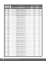
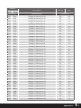
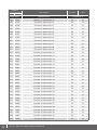
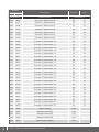
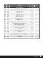
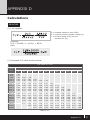
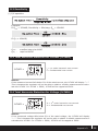
1
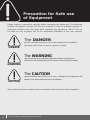
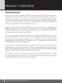
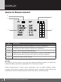
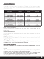
©2011 Mikro Sdn Bhd All Rights Reserved user manual PFRLCD Power Factor Regulator MODBUS-RTU 1 Precaution for Safe use of Equipment Please read the instructions carefully before operating the equipment. The following symbols will appear through out this user manual to warn of potential dangers or hazardous situation that will arises while operating the equipment. Mikro® will not be liable for any improper use of the equipment stipulated in this user manual. The DANGER DANGER symbol indicates improper use of the equipment by qualified personnel will results in serious injuries or death. The WARNING symbol indicates that potentially hazardous situation might arise if instructions are not followed that will result in serious injuries or death. WARNING The CAUTION CAUTION symbol indicates that injuries to the user or damage to the equipment will happen if the stated instructions are not followed. Only qualified personnel shall install and operates Mikro®’s Power Factor Regulator. 2 © 2011 Mikro Sdn Bhd All Rights Reserved 04 PRODUCT OVERVIEW 04 ´ Introduction 05 ´ Feature List 06 ´ Packing List 07 SETTING UP THE REGULATOR 07 ´ Installation 08 ´ Wiring 09 ´ Quick Commissioning 10 DISPLAY 10 ´ General Measurements 11 ´ Alarm Status 12 ´ Harmonics Table and Graph 13 SETTINGS 13 14 14 14 14 15 15 15 16 17 17 17 17 ´ ´ ´ ´ ´ ´ ´ ´ ´ ´ ´ ´ ´ Switching Program Target Power Factor Sensitivity Reconnection Time C/K Rated Step Coefficient Signal Contact Fan Alarm Phase Detection Automatic CT Polarity Correction Restore to Default Settings Password 18 COMMUNICATION 19 MAINTENANCE 20 APPENDIX 18 ´ Communication Setup 19 ´ Maintenance 19 ´ Getting Technical Support 20 22 35 36 ´ ´ ´ ´ Appendix Appendix Appendix Appendix A: Regulator Specification B: ModBus-RTU Table C: Setting Parameters D: Calculations ▪ C/K (C/K Table) ▪ Sensitivity ▪ %THDI and %THDV Contents 3 PRODUCT OVERVIEW Introduction Mikro®’s power factor regulator PFRLCD is designed to detect and compensate displacement power factor caused by inductive load by switching in banks of capacitors. As oppose to traditional regulator that only measures reactive power on a single phase basis but compensates three phases, the PFRLCD Three Phase model is a true three phase system as reactive power of all three phases are measured individually and compensated optimally. Mikro®’s power factor regulator PFRLCD also provides flexibility in configuring (or disabling) different levels of alarms. The alarms then can be linked to a dedicated signal contact to alert the users of potential issues such as under compensation (thus avoiding penalty charges from the utilities). As the name suggest, Mikro®’s power factor regulator PFRLCD provides the user with a 2 inch wide, 64 x 128 dot matrix LCD for displaying its various measurement parameters such as: frequency, voltage, current, THD, active, reactive, apparent power and temperature. The dot matrix LCD allows up to 31st voltage and current harmonics to be display in graphical and table form. As per the other Mikro®’s power factor regulator series, it includes the automatic C/K and rated step size detection feature for ease of commissioning for typical inductive loads. Taking advantage of the dot matrix LCD, the PFRLCD also provides a guided step-by-step commissioning menu that enables fast setup. The regulator extends its connectivity by adopting the Modbus-RTU protocol. Through the use of RS485 standard protocol, the user will be able to network the regulator with other IEDs that links to a center monitoring station. 4 © 2011 Mikro Sdn Bhd All Rights Reserved Feature List 2” inch, 64 x 128 dot matrix LCD display with back lighting Three phase and single phase detection of reactive power 12 (or 8 for 8 step model) output with two additional independent contact for signal alarm output and fan output Three phase compensation mode based on: Optimum Demand Selected Phase Highest Load 5 different switch program: Automatic Linear Four Quadrant Rotational Manual Automatic detection of C/K and rated step value Automatic Current Transformer polarity correction* Step-by-step guided commissioning No Voltage release Measurement Parameters: Active, Reactive, Apparent Power Temperature Phase Voltage and Phase Current Frequency Power Factor and Displacement Power Factor (Cos φ) %THDV and %THDI Various configurable alarm settings (can be disable) %THDI Under Compensation Over Compensation Under Current Over Current Under Voltage Over Voltage Over Temperature Rated Step Detection Error Current Transformer Polarity Error* Alarm linked signal contact Programmable fan control Modbus-RTU communication support * Available in single phase models only. Product Overview Context 5 Packing List No Description Quantity 1 PFRLCD Power Factor Regulator 1 2 Thermistor 1 3 Thermistor holder 1 PF PO RL WE CD RF AC TO R RE GU LA TO R 1 2 3 6 © 2011 Mikro Sdn Bhd All Rights Reserved Setting Up The Regulator Installation DANGER GUL LCDTOR RE PFWRER FAC ATO R PO *Please mount the regulator with sufficient spacing (at least 50mm clearance) between other electrical instruments. This is to prevent difficulty in accessing and wiring the regulator. Setting Up The Regulator 7 Wiring Diagram PFRLCD Connection diagram for 3 Phase 12 Step model P1 L1 LOAD P2 P1 DANGER P2 FUSE L2 L3 N P2 P1 32 44 43 42 41 40 39 38 37 36 35 34 33 N L1 L2 L3 In Out CT2 In Out CT3 PFR LCD N L AUX 110-240V~10VA 50/60Hz FUSE In Out CT1 K12 1 2 3 4 5 6 7 8 9 10 1112 FAN SIG 31 30 24 23 14 13 12 11 10 9 8 7 6 5 4 3 2 1 20 21 22 SIG FAN NRP P+ GND T1 T2 Thermistor K2 K1 RS485 Modbus-RTU PFRLCD Connection diagram for Single Phase 12 Step model P1 P2 LOAD L1 L2 L3 N FUSE 32 44 43 42 41 40 39 38 37 36 35 34 33 N L1 PFR LCD N L AUX 110-240V~10VA 50/60Hz K12 1 2 3 4 5 6 7 8 9 10 11 12 FAN SIG FUSE In Out CT1 31 30 24 23 14 13 12 11 10 9 8 7 6 5 4 3 2 1 20 21 22 K1 © 2011 Mikro Sdn Bhd All Rights Reserved K2 8 SIG FAN NRP P+ GND T1 T2 Thermistor RS485 Modbus-RTU Quick Commissioning The regulator is pre-programmed with the most common parameters as its factory default setting. Users are normally not required to change any setting upon commissioning. If the user requires any changes in the setting, the quick commissioning feature will provide the user with a step-by-step guidance in setting up all the mandatory parameters for the regulator to function properly. 1 4 Press 8 8 Press button, then press or to set the value. To navigate to the next page, press or to select ““, then press button. button from Home menu. 8 2 5 8 Press or button to navigate to the following pages. Press button to confirm your selection. To navigate to the next page, press or to select ““, then press button. 8 3 6 8 Press button, then press or to set the value. To navigate to the next page, press or to select ““, then press button. 8 8 Press button to confirm the selection, and then the press or to set the value. Back to the Main menu, press or to select ““, then press button. 8 Setting Up The Regulator 9 DISPLAY General Measurement 2 3 1 4 No 5 Description 1 Shows the phase that the regulator is currently measuring 2 Indicates the load condition (inductive or capacitive) 3 Alarm, Fan & Keylock status indication 4 Measurement (displacement power factor, current & temperature) and setting parameters (target power factor & switching program) 5 Shows the status of the outputs NOTES: By pressing the Exit button, user can cycle between different phases to display the respective phase parameters (applicable for three phase models). Detail measurements of other power parameters such as phase voltages, phase currents, active power, reactive power, apparent power, frequency, alarm status and temperature can be intuitively access via the sub menus (measurements). 10 © 2011 Mikro Sdn Bhd All Rights Reserved Alarm Status When any of the alarm occurs, the regulator will display which of the alarm happen via the alarm status menu. The table below shows the details of the alarm activation/ de-activation timing. Alarm Delay Time Description Symbol Activate Deactivate Total Harmonic Distortion %THDI 5 min 2.5 min Under Current Under Current 10 s 5s 1 min Over Current Over Current 2 min Under Voltage Under Voltage 100 ms 5s No Voltage Release No Volt. Release instantaneous instantaneous Over Voltage Over Voltage 15 min 7.5 min Under Compensate Under Comp. 15 min 7.5 min Over Compensate Over Comp. 15 min 7.5 min Step Error Step Error - - CT Polarity Error CT Error 10 s 5s Over Temperature Temperature 5 min 2.5 min Under Compensate Alarm All the capacitors are connected and the power factor is lower than the set power factor. Over Compensate Alarm All the capacitors are disconnected and the power factor is higher than the set power factor. Step Error Alarm Step Error Alarm will be triggered if all the capacitor bank are detected to be invalid in Auto CK setting. CT Polarity Error Alarm Current Transformer Polarity Alarm will be triggered if the measured Active Power is negative due to wrong Current Transformer connection. No Voltage Release Alarm No Voltage Release Alarm will be triggered if the measured voltage is lower than 100V. NOTES: ▪ There will be an alarm symbol blinking when any one of the alarm is being activated. ▪ The alarm status will show which of the alarms are activated. ▪ The Fan and Signal output contact will not be turn off when any of the alarms occurs. ▪ The signal contact output is programmable to link to the desired alarm signal. ▪ CT Polarity Alarm is not applicable for the Three Phase model. Display 11 Harmonics Table and Graph The power factor regulator has the capability of displaying voltage and current harmonics up till the 31st order (fundamental frequency is considered to be 1st order). The regulator will display the harmonics frequency in graphical form (bar graph) or table form which shows the harmonics value in relative % to the fundamental frequency. 12 © 2011 Mikro Sdn Bhd All Rights Reserved SETTINGS Switching Program This setting allows the user to configure the regulator to operate in one of the following switching algorithms: 1. MANUAL This mode is typically reserved for testing the regulator when commissioning it for the first time. In this mode, the user can turn on and off the capacitor bank manually by pressing the or button. The Button will turns on and button will turns off the capacitor banks. The capacitor banks are switched in a first-in-first-out (FIFO) basis. 2. AUTOMATIC The regulator selects the most appropriate step to switch in order to achieve the target power factor in the shortest reaction time within the minimum number of steps. For equal aging of capacitor and contactor the program will select the least used step to switch in or the most used step to switch out, if there are 2 or more equally rated steps. 3. ROTATIONAL In this mode, the regulator switches the regulator in a first-in-first-out (FIFO) basis to achieve the target power factor. 4. FOUR-QUADRANT This mode is the same as automatic switching mode with the exception of that it operates in both import power and export power (regenerative) conditions. There will be no automatic CT polarity correction in this mode. 5. LINEAR In this mode, the regulator switches the regulator in a first-in-last-out (FILO) switching sequence to achieve the target power factor. NOTES: ▪ For single phase model, in automatic, rotational and linear switch program, all the capacitor banks will be disconnected if the measured power flow is regenerative. ▪ For three phase model, three phase detection mode and in automatic, rotational and linear switch program, all the capacitor banks will be disconnected if the measured power flow is regenerative in any of the detected phases. If phase detect is either L1, L2, L3 or max load, the capacitor will be disconnected only if the selected phase is regenerative. Settings 13 Target Power Factor The user will be able to set the target displacement power factor value from 0.8 capacitive to 0.8 inductive. The regulator will switch the capacitor banks on and off, attempting to achieve this set value. Sensitivity The sensitivity setting controls the reaction time for the regulator to switch. The reaction time to switch is dependent on the demand, step size and the sensitivity setting. A small demand, large step size and a high sensitivity setting will result in a slower switching whereas a large demand, small step size and a small sensitivity setting will result in a faster switching speed. The reaction time is counted dynamically as the demand changes providing an optimal reaction time. Please refer to appendix D.2 for more details. Reconnection Time This setting prevents the reconnection of the same capacitor bank before it is fully discharged. This parameter is usually set based on the discharge time of the largest capacitor size in used. When a step is being turned on while the reconnection time is counting down, the LCD will display the blinking step indicating that particular step is pending to turn on. C/K The C/K value determines the threshold current value for the regulator to switch (On/Off). The C/K value is determined manually via table D.1.0 (Appendix D.1) base on the smallest capacitor bank size, system voltage and CT ratio. The regulator can automatically detect the C/K value by setting it to auto. 14 © 2011 Mikro Sdn Bhd All Rights Reserved Rated Step Coefficient The rated step setting allows the user to program the outputs in accordance to the installed capacitor bank size. When the step is set to be fixed, the output will be turn on and will not be part of the switching. If the C/K setting is automatic, the rated step size will be determined by the regulator. Signal Contact The signal contact feature provides a way to alert the user when an abnormality condition is detected in the system. The user can link the signal contact with any of the 10 alarms available individually or collectively. e.g. If the signal contact is linked with under compensate, the under compensate alarm is enabled. When the regulator detected an under compensate condition, the alarm will trigger and the signal contact will switch. Fan Mikro’s PFRLCD regulator provides flexible settings for the fan output. There are four options that can be configured as below: Setting Description None Fan output permanently off. Fixed On Fan output permanently on. Output On Fan output will turn on when any of the output turns on (including fixed step). Temperature (Setting range = 20 oC-35 oC) Fan output will turn on when the temperature exceed user set value. Settings 15 Alarm The list of available alarm and its setting range are shown below: Alarm Setting %THDI 1 Under Current Over Current User Set Range Disconnect all steps 50 % 20 – 300 % or OFF 0.15 A 0.01 – 0.15 A or OFF 5.5 A 5.50 – 7.00 A or OFF 204 V 195 – 204 V or OFF 263 V 253 – 264 V or OFF OFF ON/OFF OFF ON/OFF OFF ON/OFF OFF ON/OFF Disconnect all steps - - Disconnect all steps 65 oC 36 – 70 oC or OFF 1 Disconnect all steps 2 1 Under Compensate Over compensate Step Error Default setting 2 Under Voltage Over Voltage Actions 5 5 3,5 CT Polarity Error 4 (Single Phase only) No Voltage Release Over Temperature 16 6 1 1 The measured value must exceed the set limit value to activate. 2 The measured value must be lower than the set limit value to activate. 3 If all the rated steps are set to fixed, there will be no step error alarm. 4 There will be no CT polarity alarm in Four-Quadrant mode or Three Phase model. 5 In manual mode, there will be no under compensate alarm, over compensate alarm and step error alarm. 6 The alarm will activate if any of the phase is below 100 VAC. © 2011 Mikro Sdn Bhd All Rights Reserved Phase Detection For the three phase model, the user has the options to select the method to detect and compensate the displacement power factor as desired. The user can choose to set L1, L2, L3, maximum load or three phases. For maximum load setting, the regulator will compensate base on the phase that has the maximum load. For the three phase setting, the regulator will calculate the demand for all 3 phases and consolidate it for optimum compensation. Automatic CT Polarity Correction The automatic CT polarity correction automatically corrects the reversed connection of the current transformer in terms of measured parameters and compensation calculation. This feature is not available for the four quadrant switching program as the regulator would not be able to distinguish the reversed connection of the current transformer. The automatic CT polarity correction is only available for single phase model. Restore Default Settings The user can reset to default factory setting by pressing all 2 buttons (down and up) simultaneously for 5 seconds. The user will have 3 options, reset settings, reset password and reset settings and password to choose from. Refer to appendix C for the factory default value. Password When the regulator is locked, the user will be required to key in the password when attempting to change any settings of the regulator (the user will still be able to view the measurement parameters and alarm status). The user has the options to reset the password by pressing all 2 buttons (down and up) simultaneously for 5 seconds. The default password is 0,0,0,0. The regulator will lock when it is idle for more than 5 minutes (a lock symbol appear when locked). Settings 17 COMMUNICATION Communication Setup The regulator supports the Modbus-RTU protocol. The protocol uses a master/slave method where the regulator is the slave device. The data’s are transmitted serially via the RS485 protocol. The user can connect a RS485 to RS232 adapter to establish a communication through the PC serial port. The supported function codes are 03 (read holding register), 04 (read input register), 06 (write single register) and 16 (write multiple registers). The default parity mode is Even and None parity requires 2 stop bit. Refer to the connection diagram to setup the communication. 1 to 32 PFR PF PO RL WER PF CD FA CT OR PO RE GU LATO RL WER PF CD FA CT OR PO RE GU R LATO R RL WER CD FA CT OR RE GU LATO R RS232 / 485 Modbus-RTU 2-wire converter PF PO RL WER PF CD FA CT OR PO RE GU LATO R RL WER CD FA CT OR RE GU LATO R Shield Cable Host 18 © 2011 Mikro Sdn Bhd All Rights Reserved Remote Set Enabling the Remote Set allows the remote terminal to read and write the power factor regulator setting via Modbus RTU, otherwise the setting data can only be read. Enabling feature can only be done at the panel unit. Baudrate There are 2 baudrates available for selection. 1) 9600bps 2) 19200bps Parity Bit There are 3 selections for parity bit set in data frame. 1) None 2)Odd 3)Even Maintenance There are no user serviceable parts on this product. Please do not open the product, as opening it will void the warranty. Please contact your nearest sales representative if the product requires any service or repair. Getting Technical Support For technical support, you can obtain assistances via : Address : Mikro Sdn Bhd No. 1, Jalan TP 7/7, Sime UEP Industrial Park, 40400 Shah Alam, Selangor, Malaysia. Tel : Fax : Technical Hotline : Website : +6 03 5192 7155 +6 03 5192 7166 1-800-88-1113 (Toll Free) +6 016 201 4801 www.itmikro.com Communication 19 APPENDIX A Regulator Specification CURRENT INPUT (EACH PHASE) Nominal Current Operating Limits Rated frequency 5 A rms 0.01-10 A rms 50 Hz or 60 Hz VOLTAGE INPUT (EACH PHASE with respect to neutral) Nominal Voltage Operating Limits Consumption Rated Frequency Category 230 VAC 0 - 277 V L-N 0.05 VA 50 Hz or 60 Hz III * THERMISTOR INPUT Thermistor Temperature range 0 – 100 °C AUXILIARY Auxiliary Input Voltage Range Rated Voltage Range Consumption Rated Frequency 85-265 V rms 110-230V rms 10 VA max 50 Hz/ 60 Hz RELAY OUTPUT Number of outputs Contact arrangement Contact rating Expected electrical life Expected mechanical life 14 NO contact type 5 A , 250 VAC ( COS φ = 1) 100,000 operations at rated current 5 x 10⁶ operations CONTROL RANGE Target Power factor C/K setting Sensitivity Reconnection time Switching program Rated step coefficient Detection mode Fan Setting Signal Contact 0.80 Inductive – 0.80 Capacitive 0.03 – 1.20 / Automatic detect 5 – 300 s/ Step 5 – 240 s Automatic/ Manual/ Four-quadrant/ Rotational/ Linear 0/ 1/ 2/ 3/ 4/ 5/ 6/ 8/ 12/ 16/ Fixed L1 / L2 / L3 / Max Load / Three Phase Fixed on / Output On / Temperature / None Linked to 10 different programmable alarm / None ALARM SETTING RANGE %THDI Over Voltage Under Voltage Over Current Under Current Under Compensate Over Compensate **CT Polarity Error Step Error Over Temperature 20 20 – 300 % / OFF 253 – 264 V/ OFF 195 – 204 V/ OFF 5.50 – 7.00 A/ OFF 0.01 – 0.15 A/ OFF On / OFF On / OFF On / OFF On / OFF 36 – 70 °C / OFF © 2011 Mikro Sdn Bhd All Rights Reserved DISPLAY %THDI and %THDV Harmonics Resolution Active power Reactive power Apparent power Voltage Current Temperature Frequency Power Factor Displacement Power Factor 0 – 500 % Up to 31st Harmonics 0 – 3000 W 0 – 3000 VAR 0 – 3000 VA 0 – 300 VAC 0.00 – 10.0 A rms 0 – 100 °C 45 – 65 Hz -1.00 – 1.00 -1.00 – 1.00 ** This feature is not available in Three phase model. MECHANICAL Mounting Panel mounting Dimension (h x w x d) 144mm x 144mm x 122mm IP Protection IP54 Front Panel, IP20 Meter Body Approximate weight 1.2 kg (for three phase model), 1 kg for (single phase model) ENVIRONMENT CONDITIONS Temperature -5 °C to +55 °C Humidity 56 days at 93%RH and 40°C non-condensing Pollution Degree II Dielectric Withstand IEC61010-1 Altitude 2000 m EMC ESD (Electrostatic Discharge) IEC61000-4-2 CD Level II AD Level III EFT (Electric Fast Transient) IEC61000-4-4 Level III Surge IEC61000-4-5 Level II Conducted Immunity IEC61000-4-6 Level III Magnetic Field Immunity IEC61000-4-8 Level III Radiated Field Immunity IEC61000-4-3 Level III Voltage Dip IEC61000-4-11 Conducted and Radiated Emission EN55011 Harmonics IEC61000-3-2 Flicker Emission IEC61000-3-3 * Overvoltage installation categories per IEC 61010-1. CAT III is classified as “from equipment in fixed equipement installations, e.g., installation panels, feeders and short branch circuits and lighting systems in large buildings”. Appendix A 21 APPENDIX B ModBus Table FORMAT DEFINITION FORMAT TYPE DESCRIPTION F1 Power Measurement & Calibration IEEE 754 single precision floating point representation. The floating point (4-bytes) data are transferred by means of first 2 bytes (Least significant) located at modbus address I, followed by the next 2 bytes (Most significant) at modbus address i+1 F2 3 phase Voltage and Current Harmonic Measurement b15-b0:Unsigned Integer. The value is expressed as x/10 %. Eg. 1000 means 100.0%. negative value (-1) in harmonic indicates that the measured rms voltage is below 5% of the rated voltage (230v) ie. 11.5V or measured rms current is below 2% of the rated current (5A) ie 0.1A. Max value for Voltage harmonic and current harmonic is 5000 (500%). Harmonic value which is higher then 500% will be capped as 500% F3 Product Information High byte: First ASCII Character b15-b8: Unsigned Char. Low byte : Second ASCII Character b7-b0: Unsigned char F4 Switching Program & C/K Setting High byte: Switching Program b15-b12: don’t care b11-b8 : 0: Manual 1: Rotational 2: Four-quadrant 3: Automatic 4: Linear Low byte: C/K Setting b7-b0: Unsigned Char. The valid range is from 3 to 121(AutoCk). The value is expressed as x/100 i.e. 3 means 0.03. 22 © 2011 Mikro Sdn Bhd All Rights Reserved F5 Reconnection Time & Power factor Setting High byte: Reconnection time b15-b8 :Unsigned Char. The valid range is from 5 to 240. Low byte: Power Factor Setting b7-b0 :Unsigned Char. The valid range is from 80 to 120. Cos φ Value --------------------------0.80 Ind 80 0.98 Ind 98 1.00 Res 100 0.98 Cap 102 0.80 Cap 120 F6 Rated Step Coefficient High byte: Step X* b15-b8: Unsigned Char. Valid values: 0, 1, 2, 3, 4, 5, 6, 8, 12, 16, 255(Fixed) Low byte Step X + 1* b7-b0: Unsigned Char. Valid values: 0, 1, 2, 3, 4, 5, 6, 8, 12, 16, 255(Fixed) * For 8 steps model, rated step coefficient for step 9-12 is not applicable F7 Detection Phase Setting High byte: Detection Phase* b15-b12: don’t care b11-b8: 0: L1 1: L2 2: L3 3: 3 Phase 4: Maximum load Low byte: Don’t care *It is not applicable for single phase model F8 Alarm setting for %THDI Limit b15-b0 :Unsigned int. The valid range is from 20 to 300. 0 is for Off. The value is expressed in % i.e. 20 mean 20%. F9 Alarm setting for Under Current and Over Current Limit High byte: Under Current b15-b8 : Unsigned Char. The valid range is from 1 to 15. 0 is for Off. The value is expressed as x/100 i.e. 1 means 0.01. Low byte: Over Current b7-b0: Unsigned Char. The valid range is from 1 to 16. 0 is for Off. This value is expressed as (x + 54)/10. i.e. 1 means 5.5 & 11 means 6.5. Appendix B 23 F10 Alarm setting for Under Voltage and Over Voltage Limit High byte: Under Voltage Limit b15-b8: Unsigned Char. The valid range is from 195 to 204. 0 is for Off. Low byte: Over Voltage Limit b7-b0: Unsigned Char. The valid range is from 1 to 12. 0 is for Off. This value is expressed as (x + 252. i.e 1 means 253 and 12 means 264. F11 Fan Temperature and Alarm setting for High Temperature Limit High byte: Fan Temperature Limit b15-b8: Unsigned Char. The valid range is from 20 to 35. Low byte: Over Temperature Limit b7-b0: Unsigned Char. The valid range is from 36 to 70. 0 is for Off. F12 Slave Address and Set Baud Rate High byte: Slave Address b15-b8: Unsigned Char Low byte: Set Baud Rate b7-b1: don’t care b0: Baud Rate 0: 19200 bps 1: 9600 bps F13 Set Parity and Fan Setting High byte: Set Parity b15-b10: don’t care b9-b8: 0: None 1: Odd 2: Even Low byte: Fan setting b7-b4: don’t care b3-b0: b0: None b1: Fixed on b2: Output ON b3: Temperature 24 © 2011 Mikro Sdn Bhd All Rights Reserved F14 Signal Contact and Alarm Settings High byte: Signal contact (Alarm and None) b15-b11: don’t care b10-b8: 1: Alarm 2: None Low byte : Alarm Settings for Under Compensate, Over Compensate, Step Error and CT polarity error b7-b4 : don’t care b3-b0 : ‘0’ = Off ; ‘1’ = On b0: Under compensate b1: Over compensate b2: Step error b3: CT polarity error* *Only available in single phase model F15 Signal Contact Alarm Linkage 2 and Signal Contact Alarm Linkage 1 Hight byte: Signal Contact Alarm Linkage 1 b15-b8: Unsigneid Char. ‘1’: Linked to signal contact ‘0’: Not linked to signal contact b8: %THDI b9: Under Current b10: Over Current b11: Under Voltage b12: Over Voltage b13: Under Compensate b14: Over Compensate b15: Step Error Alarm Low byte: Signal Contact Alarm Linkage 2 b7-b2: don’t care b1-b0 : ‘1’: Linked to signal contact ‘0’: Not linked to signal contact b0: CT Polarity Error * b1: Over Temperature *Only available in single phase model F16 Sensitivity b15-b0: Unsigned Int. The valid range is from 5 to 300. F17 Reserved b15-b0: Reserved Appendix B 25 F18 Alarm Status High byte: Alarm Status High Byte b15-b8: b8 : %THDI Alarm Status b9 : Under Current Alarm Status b10: Over Current Alarm Status b11: Under Voltage Alarm Status b12: Over Voltage Alarm Status b13: Under Compensate Alarm Status b14: Over Compensate Alarm Status b15: Step Error Alarm Status Low byte: Alarm Status Low Byte b3-b0: b0 : CT Polarity Alarm Status b1 : Temperature High Status Alarm b2 : Low Volt Release Alarm Status b7-b4: don’t care F19 Displacement PF b15-b0: Signed Integer from -100 to 100. The value is expressed as x/100. Eg. -86 means -0.86. F20 Step Output Status b15-b12: don’t care b11-b0 : ‘1’: Step Off ‘0’: Step On example: b0 for step 1 status note: b8 to b11 is not applicable for 8 steps model. 26 © 2011 Mikro Sdn Bhd All Rights Reserved Modbus Database Address Dec Description Hex Read Only Product Information Format Unit Functions 4 0 0000 Model Description 1 & 2 F3 00 1 0001 Model Description 3 & 4 F3 08 2 0002 Model Description 5 & 6 F3 00 3 0003 Model Description 7 & 8 F3 xx1 4 0004 Model Description 9 & 10 F3 xx2 5 0005 Model Description 11 & 12 F3 xx3 6 0006 Manufacturer 1 & 2 F3 7 0007 Manufacturer 3 & 4 F3 8 0008 Manufacturer 5 & 6 F3 9 0009 Firmware Version 1 & 2 F3 10 000A Firmware Version 3 & 4 F3 11 000B Number Of Outputs F3 xx4 12 000C Phase model F3 xx3 13 000D Frequency model F3 xx5 14 000E Reserved F17 15 000F Reserved F17 16 0010 Reserved F17 NOTES: 1 For 8 steps model, ‘xx’ = <space><space> For 12 steps model, ‘xx’ = <space> ‘1’ 2 For 8 steps model, ‘xx’ = ‘80’ For 12 steps model, ‘xx’ = ‘20’ 3 For single phase model, ‘xx’ = ‘P1’ For three phase model, ‘xx’ = ‘P3’ 4 For 8 steps model, ‘xx’ = <space> ‘8’ For 12 steps model, ‘xx’ = ‘12’ 5 For 50Hz model, ‘xx’ = ‘50’ For 60Hz model, ‘xx’ = ‘60’ Appendix B 27 Address Dec Hex Read Only 28 17 0011 19 21 23 25 Description Measurement Format Unit Functions 4 Frequency F1 Hz 0013 Phase Voltage A F1 Vrms 0015 Phase Voltage B F1 Vrms 0017 Phase Voltage C F1 Vrms 0019 Phase Current A F1 Irms 27 001B Phase Current B F1 Irms 29 001D Phase Current C F1 Irms 31 001F Active Power Phase A F1 W 33 0021 Reactive Power Phase A F1 VAR 35 0023 Apparent Power Phase A F1 VA 37 0025 Power Factor Phase A F1 39 0027 Active Power Phase B F1 W 41 0029 Reactive Power Phase B F1 VAR 43 002B Apparent Power Phase B F1 VA 45 002D Power Factor Phase B F1 47 002F Active Power Phase C F1 W 49 0031 Reactive Power Phase C F1 VAR 51 0033 Apparent Power Phase C F1 VA 53 0035 Power Factor Phase C F1 55 0037 Total Active Power F1 W 57 0039 Total Reactive Power F1 VAR 59 003B Total Apparent Power F1 VA 61 003D Total Power Factor F1 63 003F Fundamental Active Power Phase A F1 W 65 0041 Fundamental Active Power Phase B F1 W 67 0043 Fundamental Active Power Phase C F1 W 69 0045 Fundamental Reactive Power Phase A F1 VAR 71 0047 Fundamental Reactive Power Phase B F1 VAR 73 0049 Fundamental Reactive Power Phase C F1 VAR 75 004B Harmonic Active Power Phase A F1 W 77 004D Harmonic Active Power Phase B F1 W 79 004F Harmonic Active Power Phase C F1 W 81 0051 Harmonic Reactive Power Phase A F1 VAR 83 0053 Harmonic Reactive Power Phase B F1 VAR © 2011 Mikro Sdn Bhd All Rights Reserved Address Dec Hex Read Only 85 0055 87 89 Description Measurement Format Unit Functions 4 Harmonic Reactive Power Phase C F1 VAR 0057 Total Voltage Harmonic Phase A F1 Vrms 0059 Total Voltage Harmonic Phase B F1 Vrms 91 005B Total Voltage Harmonic Phase C F1 Vrms 93 005D Total Current Harmonic Phase A F1 Irms 95 005F Total Current Harmonic Phase B F1 Irms 97 0061 Total Current Harmonic Phase C F1 Irms 99 0063 Voltage A Harmonics 0 F2 % 100 0064 Voltage A Harmonics 1 F2 % 101 0065 Voltage A Harmonics 2 F2 % 102 0066 Voltage A Harmonics 3 F2 % 103 0067 Voltage A Harmonics 4 F2 % 104 0068 Voltage A Harmonics 5 F2 % 105 0069 Voltage A Harmonics 6 F2 % 106 006A Voltage A Harmonics 7 F2 % 107 006B Voltage A Harmonics 8 F2 % 108 006C Voltage A Harmonics 9 F2 % 109 006D Voltage A Harmonics 10 F2 % 110 006E Voltage A Harmonics 11 F2 % 111 006F Voltage A Harmonics 12 F2 % 112 0070 Voltage A Harmonics 13 F2 % 113 0071 Voltage A Harmonics 14 F2 % 114 0072 Voltage A Harmonics 15 F2 % 115 0073 Voltage A Harmonics 16 F2 % 116 0074 Voltage A Harmonics 17 F2 % 117 0075 Voltage A Harmonics 18 F2 % 118 0076 Voltage A Harmonics 19 F2 % 119 0077 Voltage A Harmonics 20 F2 % 120 0078 Voltage A Harmonics 21 F2 % 121 0079 Voltage A Harmonics 22 F2 % 122 007A Voltage A Harmonics 23 F2 % 123 007B Voltage A Harmonics 24 F2 % 124 007C Voltage A Harmonics 25 F2 % 125 007D Voltage A Harmonics 26 F2 % Appendix B 29 Address Dec Hex Read Only 126 30 Description Measurement Format Unit Functions 4 007E Voltage A Harmonics 27 F2 % 127 007F Voltage A Harmonics 28 F2 % 128 0080 Voltage A Harmonics 29 F2 % 129 0081 Voltage A Harmonics 30 F2 % 130 0082 Voltage A Harmonics 31 F2 % 131 0083 Voltage B Harmonics 0 F2 % 132 0084 Voltage B Harmonics 1 F2 % 133 0085 Voltage B Harmonics 2 F2 % 134 0086 Voltage B Harmonics 3 F2 % 135 0087 Voltage B Harmonics 4 F2 % 136 0088 Voltage B Harmonics 5 F2 % 137 0089 Voltage B Harmonics 6 F2 % 138 008A Voltage B Harmonics 7 F2 % 139 008B Voltage B Harmonics 8 F2 % 140 008C Voltage B Harmonics 9 F2 % 141 008D Voltage B Harmonics 10 F2 % 142 008E Voltage B Harmonics 11 F2 % 143 008F Voltage B Harmonics 12 F2 % 144 0090 Voltage B Harmonics 13 F2 % 145 0091 Voltage B Harmonics 14 F2 % 146 0092 Voltage B Harmonics 15 F2 % 147 0093 Voltage B Harmonics 16 F2 % 148 0094 Voltage B Harmonics 17 F2 % 149 0095 Voltage B Harmonics 18 F2 % 150 0096 Voltage B Harmonics 19 F2 % 151 0097 Voltage B Harmonics 20 F2 % 152 0098 Voltage B Harmonics 21 F2 % 153 0099 Voltage B Harmonics 22 F2 % 154 009A Voltage B Harmonics 23 F2 % 155 009B Voltage B Harmonics 24 F2 % 156 009C Voltage B Harmonics 25 F2 % 157 009D Voltage B Harmonics 26 F2 % 158 009E Voltage B Harmonics 27 F2 % 159 009F Voltage B Harmonics 28 F2 % © 2011 Mikro Sdn Bhd All Rights Reserved Address Dec Hex Read Only Description Measurement Format Unit Functions 4 160 00A0 Voltage B Harmonics 29 F2 % 161 00A1 Voltage B Harmonics 30 F2 % 162 00A2 Voltage B Harmonics 31 F2 % 163 00A3 Voltage C Harmonics 0 F2 % 164 00A4 Voltage C Harmonics 1 F2 % 165 00A5 Voltage C Harmonics 2 F2 % 166 00A6 Voltage C Harmonics 3 F2 % 167 00A7 Voltage C Harmonics 4 F2 % 168 00A8 Voltage C Harmonics 5 F2 % 169 00A9 Voltage C Harmonics 6 F2 % 170 00AA Voltage C Harmonics 7 F2 % 171 00AB Voltage C Harmonics 8 F2 % 172 00AC Voltage C Harmonics 9 F2 % 173 00AD Voltage C Harmonics 10 F2 % 174 00AE Voltage C Harmonics 11 F2 % 175 00AF Voltage C Harmonics 12 F2 % 176 00B0 Voltage C Harmonics 13 F2 % 177 00B1 Voltage C Harmonics 14 F2 % 178 00B2 Voltage C Harmonics 15 F2 % 179 00B3 Voltage C Harmonics 16 F2 % 180 00B4 Voltage C Harmonics 17 F2 % 181 00B5 Voltage C Harmonics 18 F2 % 182 00B6 Voltage C Harmonics 19 F2 % 183 00B7 Voltage C Harmonics 20 F2 % 184 00B8 Voltage C Harmonics 21 F2 % 185 00B9 Voltage C Harmonics 22 F2 % 186 00BA Voltage C Harmonics 23 F2 % 187 00BB Voltage C Harmonics 24 F2 % 188 00BC Voltage C Harmonics 25 F2 % 189 00BD Voltage C Harmonics 26 F2 % 190 00BE Voltage C Harmonics 27 F2 % 191 00BF Voltage C Harmonics 28 F2 % 192 00C0 Voltage C Harmonics 29 F2 % 193 00C1 Voltage C Harmonics 30 F2 % Appendix B 31 Address Dec Hex Read Only 32 Description Measurement Format Unit Functions 4 194 00C2 Voltage C Harmonics 31 F2 % 195 00C3 Current A Harmonics 0 F2 % 196 00C4 Current A Harmonics 1 F2 % 197 00C5 Current A Harmonics 2 F2 % 198 00C6 Current A Harmonics 3 F2 % 199 00C7 Current A Harmonics 4 F2 % 200 00C8 Current A Harmonics 5 F2 % 201 00C9 Current A Harmonics 6 F2 % 202 00CA Current A Harmonics 7 F2 % 203 00CB Current A Harmonics 8 F2 % 204 00CC Current A Harmonics 9 F2 % 205 00CD Current A Harmonics 10 F2 % 206 00CE Current A Harmonics 11 F2 % 207 00CF Current A Harmonics 12 F2 % 208 00D0 Current A Harmonics 13 F2 % 209 00D1 Current A Harmonics 14 F2 % 210 00D2 Current A Harmonics 15 F2 % 211 00D3 Current A Harmonics 16 F2 % 212 00D4 Current A Harmonics 17 F2 % 213 00D5 Current A Harmonics 18 F2 % 214 00D6 Current A Harmonics 19 F2 % 215 00D7 Current A Harmonics 20 F2 % 216 00D8 Current A Harmonics 21 F2 % 217 00D9 Current A Harmonics 22 F2 % 218 00DA Current A Harmonics 23 F2 % 219 00DB Current A Harmonics 24 F2 % 220 00DC Current A Harmonics 25 F2 % 221 00DD Current A Harmonics 26 F2 % 222 00DE Current A Harmonics 27 F2 % 223 00DF Current A Harmonics 28 F2 % 224 00E0 Current A Harmonics 29 F2 % 225 00E1 Current A Harmonics 30 F2 % 226 00E2 Current A Harmonics 31 F2 % 227 00E3 Current B Harmonics 0 F2 % © 2011 Mikro Sdn Bhd All Rights Reserved Address Dec Hex Read Only Description Measurement Format Unit Functions 4 228 00E4 Current B Harmonics 1 F2 % 229 00E5 Current B Harmonics 2 F2 % 230 00E6 Current B Harmonics 3 F2 % 231 00E7 Current B Harmonics 4 F2 % 232 00E8 Current B Harmonics 5 F2 % 233 00E9 Current B Harmonics 6 F2 % 234 00EA Current B Harmonics 7 F2 % 235 00EB Current B Harmonics 8 F2 % 236 00EC Current B Harmonics 9 F2 % 237 00ED Current B Harmonics 10 F2 % 238 00EE Current B Harmonics 11 F2 % 239 00EF Current B Harmonics 12 F2 % 240 00F0 Current B Harmonics 13 F2 % 241 00F1 Current B Harmonics 14 F2 % 242 00F2 Current B Harmonics 15 F2 % 243 00F3 Current B Harmonics 16 F2 % 244 00F4 Current B Harmonics 17 F2 % 245 00F5 Current B Harmonics 18 F2 % 246 00F6 Current B Harmonics 19 F2 % 247 00F7 Current B Harmonics 20 F2 % 248 00F8 Current B Harmonics 21 F2 % 249 00F9 Current B Harmonics 22 F2 % 250 00FA Current B Harmonics 23 F2 % 251 00FB Current B Harmonics 24 F2 % 252 00FC Current B Harmonics 25 F2 % 253 00FD Current B Harmonics 26 F2 % 254 00FE Current B Harmonics 27 F2 % 255 00FF Current B Harmonics 28 F2 % 256 0100 Current B Harmonics 29 F2 % 257 0101 Current B Harmonics 30 F2 % 258 0102 Current B Harmonics 31 F2 % 259 0103 Current C Harmonics 0 F2 % 260 0104 Current C Harmonics 1 F2 % 261 0105 Current C Harmonics 2 F2 % Appendix B 33 Address Dec Hex Read Only 34 Description Measurement Format Unit Functions 4 262 0106 Current C Harmonics 3 F2 % 263 0107 Current C Harmonics 4 F2 % 264 0108 Current C Harmonics 5 F2 % 265 0109 Current C Harmonics 6 F2 % 266 010A Current C Harmonics 7 F2 % 267 010B Current C Harmonics 8 F2 % 268 010C Current C Harmonics 9 F2 % 269 010D Current C Harmonics 10 F2 % 270 010E Current C Harmonics 11 F2 % 271 010F Current C Harmonics 12 F2 % 272 0110 Current C Harmonics 13 F2 % 273 0111 Current C Harmonics 14 F2 % 274 0112 Current C Harmonics 15 F2 % 275 0113 Current C Harmonics 16 F2 % 276 0114 Current C Harmonics 17 F2 % 277 0115 Current C Harmonics 18 F2 % 278 0116 Current C Harmonics 19 F2 % 279 0117 Current C Harmonics 20 F2 % 280 0118 Current C Harmonics 21 F2 % 281 0119 Current C Harmonics 22 F2 % 282 011A Current C Harmonics 23 F2 % 283 011B Current C Harmonics 24 F2 % 284 011C Current C Harmonics 25 F2 % 285 011D Current C Harmonics 26 F2 % 286 011E Current C Harmonics 27 F2 % 287 011F Current C Harmonics 28 F2 % 288 0120 Current C Harmonics 29 F2 % 289 0121 Current C Harmonics 30 F2 % 290 0122 Current C Harmonics 31 F2 % 291 0123 Alarm Status F18 292 0124 Displacement PF1 F19 293 0125 Displacement PF2 F19 294 0126 Displacement PF3 F19 295 0127 Step Output Status F20 © 2011 Mikro Sdn Bhd All Rights Reserved Address Dec Hex Read/Write 296 Description Control Parameters Format Unit Functions 3, 6, 16 0128 Switching Program & C/K Setting F4 297 0129 Reconnection Time and Target Power Factor F5 298 012A Rated Step 1 and 2 F6 299 012B Rated Step 3 and 4 F6 300 012C Rated Step 5 and 6 F6 301 012D Rated Step 7 and 8 F6 302 012E Rated Step 9 and 10 F6 303 012F Rated Step 11 and 12 F6 304 0130 Detection Phase F7 305 0131 Alarm Setting for Under Current and Over Current F9 306 0132 Alarm setting for Under Voltage and Over Voltage F10 307 0133 Fan Temperature and Alarm Setting for Over Temperature Limit F11 308 0134 Set Slave Address and Baud Rate F12 309 0135 Set Parity and Fan setting F13 310 0136 Sensitivity F16 311 0137 Alarm setting for %THDI Limit F8 312 0138 Reserved 313 0139 Signal Contact and Alarm Settings F14 314 013A Signal Contact Alarm Linkage 2 and Signal Contact Alarm Linkage 1 F15 315 013B Reserved F17 316 013C Reserved F17 Appendix B 35 APPENDIX C Setting Parameters CONTROL SETTING PARAMETERS Target Power factor 0.98 Inductive C/K setting Auto Sensitivity 45 s Reconnection time 30 s Switching program Auto mode Rated step coefficient Detection mode Fan Setting Signal Contact ALARM SETTING PARAMETERS %THDI Over Voltage 1 for all steps Max Load None None DEFAULT VALUE 50 % 263 VAC Under Voltage 204 VAC Over Current 5.50 A rms Under Current 0.15 A rms Under Compensate Off Over Compensate Off CT Polarity Error Off Step Error Over Temperature COMMUNICATION SETTING PARAMETERS Slave Address Baud Rate Parity Communication Enable 36 DEFAULT VALUE © 2011 Mikro Sdn Bhd All Rights Reserved Off 65 °C DEFAULT VALUE 1 19200 bps Even Off APPENDIX D Calculations D.1 C/K (i) C /K equation: Q = smallest capacitor step (VAR) V = nominal primary system voltage (V) I = primary rating of the current transformer (A) Example: If Q = 20kVAR, V = 415V, I = 850A then, (i) Computed C/K value as show below: C/K Value for 415V Smallest Capacitor in (kVAR) C.T Ratio 5 10 12.5 15 20 25 30:5 50:5 75:5 100:5 150:5 1.16 0.70 0.46 0.35 0.23 0.93 0.70 0.46 1.16 0.87 0.58 1.04 0.70 0.93 1.16 200:5 250:5 300:5 400:5 500:5 0.17 0.14 0.12 0.09 0.07 0.35 0.28 0.23 0.17 0.14 0.43 0.35 0.29 0.22 0.17 0.52 0.42 0.35 0.26 0.21 0.70 0.56 0.46 0.35 0.28 600:5 800:5 1000:5 1500:5 2000:5 0.06 0.04 0.03 0.12 0.09 0.07 0.05 0.03 0.14 0.11 0.09 0.06 0.04 0.17 0.13 0.10 0.07 0.05 0.03 0.03 0.03 0.04 0.03 0.03 2500:5 3000:5 4000:5 30 40 50 60 100 150 0.87 0.70 0.58 0.43 0.35 1.04 0.83 0.70 0.52 0.42 1.11 0.93 0.70 0.56 1.16 0.87 0.70 1.04 0.83 0.23 0.17 0.14 0.09 0.07 0.29 0.22 0.17 0.12 0.09 0.35 0.26 0.21 0.14 0.10 0.46 0.35 0.28 0.19 0.14 0.58 0.43 0.35 0.23 0.17 0.70 0.52 0.42 0.28 0.21 1.16 0.87 0.70 0.46 0.35 1.04 0.70 0.52 0.06 0.05 0.03 0.07 0.06 0.04 0.08 0.07 0.05 0.11 0.09 0.07 0.14 0.12 0.09 0.17 0.14 0.10 0.28 0.23 0.17 0.42 0.35 0.26 Table D.1.0 Context Appendix D 37 D.2 Sensitivity (i) C/K equation: Example: If Q1st = 15kVAR, Sensitivity = 60s/step, Qrq = 15kVAR If Qrq = 45kVAR, Q1st : smallest step size kVAR Qrq : required kVAR D.3 Total Harmonic Distortion for Current (%THDI) %THDI = in = nth order harmonic rms current i1 = fundamental rms current NOTES: If the measured current falls below 2% of the rated current, the %THDI will display “---“. This is because the regulator will not be able to obtain a reliable measurement to calculate the %THDI. For %THDI > 500%, %THDI will be capped at 500% D.4 Total Harmonic Distortion for Voltage (%THDV) %THDI = Vn = nth order harmonic rms current V1 = fundamental rms current NOTES: If the measured voltage falls below 5% of the rated voltage, the %THDV will display “---“. This is because the regulator will not be able to obtain a reliable measurement to calculate the %THDV. For %THDV > 500%, %THDV will be capped at 500% Appendix D 38