1
User Manual
16
Data Flash Access
Library
Type T04 (Pico), European Release
16 Bit Single-chip Microcontroller
RL78 Series
Installer: RENESAS_FDL_RL78_T04E_Vx.xxx
All information contained in these materials, including products and product specifications,
represents information on the product at the time of publication and is subject to change by
Renesas Electronics Corp. without notice. Please review the latest information published by
Renesas Electronics Corp. through various means, including the Renesas Technology Corp.
website (http://www.renesas.com).
www.renesas.com
R01US0055ED0112, Rev. 1.12
Dec 17, 2014
Notice
1. All information included in this document is current as of the date this document is issued. Such
information, however, is subject to change without any prior notice. Before purchasing or using
any Renesas Electronics products listed herein, please confirm the latest product information with
a Renesas Electronics sales office. Also, please pay regular and careful attention to additional
and different information to be disclosed by Renesas Electronics such as that disclosed through
our website.
2. Renesas Electronics does not assume any liability for infringement of patents, copyrights, or other
intellectual property rights of third parties by or arising from the use of Renesas Electronics
products or technical information described in this document. No license, express, implied or
otherwise, is granted hereby under any patents, copyrights or other intellectual property rights of
Renesas Electronics or others.
3. You should not alter, modify, copy, or otherwise misappropriate any Renesas Electronics product,
whether in whole or in part.
4. Descriptions of circuits, software and other related information in this document are provided only
to illustrate the operation of semiconductor products and application examples. You are fully
responsible for the incorporation of these circuits, software, and information in the design of your
equipment. Renesas Electronics assumes no responsibility for any losses incurred by you or
third parties arising from the use of these circuits, software, or information.
5. When exporting the products or technology described in this document, you should comply with
the applicable export control laws and regulations and follow the procedures required by such
laws and regulations. You should not use Renesas Electronics products or the technology
described in this document for any purpose relating to military applications or use by the military,
including but not limited to the development of weapons of mass destruction. Renesas
Electronics products and technology may not be used for or incorporated into any products or
systems whose manufacture, use, or sale is prohibited under any applicable domestic or foreign
laws or regulations.
6. Renesas Electronics has used reasonable care in preparing the information included in this
document, but Renesas Electronics does not warrant that such information is error free. Renesas
Electronics assumes no liability whatsoever for any damages incurred by you resulting from
errors in or omissions from the information included herein.
7. Renesas Electronics products are classified according to the following three quality grades:
“Standard”, “High Quality”, and “Specific”. The recommended applications for each Renesas
Electronics product depends on the product’s quality grade, as indicated below. You must check
the quality grade of each Renesas Electronics product before using it in a particular application.
You may not use any Renesas Electronics product for any application categorized as “Specific”
without the prior written consent of Renesas Electronics. Further, you may not use any Renesas
Electronics product for any application for which it is not intended without the prior written consent
of Renesas Electronics. Renesas Electronics shall not be in any way liable for any damages or
losses incurred by you or third parties arising from the use of any Renesas Electronics product for
an application categorized as “Specific” or for which the product is not intended where you have
failed to obtain the prior written consent of Renesas Electronics.
R01US0055ED0112 Rev. 1.12
User Manual
2
8. The quality grade of each Renesas Electronics product is “Standard” unless otherwise expressly
specified in a Renesas Electronics data sheets or data books, etc.
“Standard”:
Computers; office equipment; communications equipment; test and measurement
equipment; audio and visual equipment; home electronic appliances; machine
tools; personal electronic equipment; and industrial robots.
“High Quality”: Transportation equipment (automobiles, trains, ships, etc.); traffic control
systems; anti-disaster systems; anti- crime systems; safety equipment; and
medical equipment not specifically designed for life support.
“Specific”:
Aircraft; aerospace equipment; submersible repeaters; nuclear reactor control
systems;medical equipment or systems for life support (e.g. artificial life support
devices or systems), surgical implantations, or healthcare intervention (e.g.
excision, etc.), and any other applications or purposes that pose a direct threat to
human life.
9. You should use the Renesas Electronics products described in this document within the range
specified by Renesas Electronics, especially with respect to the maximum rating, operating
supply voltage range, movement power voltage range, heat radiation characteristics, installation
and other product characteristics. Renesas Electronics shall have no liability for malfunctions or
damages arising out of the use of Renesas Electronics products beyond such specified ranges.
10. Although Renesas Electronics endeavors to improve the quality and reliability of its products,
semiconductor products have specific characteristics such as the occurrence of failure at a
certain rate and malfunctions under certain use conditions. Further, Renesas Electronics products
are not subject to radiation resistance design. Please be sure to implement safety measures to
guard them against the possibility of physical injury, and injury or damage caused by fire in the
event of the failure of a Renesas Electronics product, such as safety design for hardware and
software including but not limited to redundancy, fire control and malfunction prevention,
appropriate treatment for aging degradation or any other appropriate measures. Because the
evaluation of microcomputer software alone is very difficult, please evaluate the safety of the final
products or system manufactured by you.
11. Please contact a Renesas Electronics sales office for details as to environmental matters such as
the environmental compatibility of each Renesas Electronics product. Please use Renesas
Electronics products in compliance with all applicable laws and regulations that regulate the
inclusion or use of controlled substances, including without limitation, the EU RoHS Directive.
Renesas Electronics assumes no liability for damages or losses occurring as a result of your
noncompliance with applicable laws and regulations.
12. This document may not be reproduced or duplicated, in any form, in whole or in part, without prior
written consent of Renesas Electronics.
13. Please contact a Renesas Electronics sales office if you have any questions regarding the
information contained in this document or Renesas Electronics products, or if you have any other
inquiries.
(Note 1) “Renesas Electronics” as used in this document means Renesas Electronics
Corporation and also includes its majority- owned subsidiaries.
(Note 2) “Renesas Electronics product(s)” means any product developed or manufactured
by or for Renesas Electronics.
R01US0055ED0112 Rev. 1.12
User Manual
3
Regional Information
Some information contained in this document may vary from country to country. Before using any
Renesas Electronics product in your application, please contact the Renesas Electronics office in your
country to obtain a list of authorized representatives and distributors. They will verify:
Device availability
Ordering information
Product release schedule
Availability of related technical literature
Development environment specifications (for example, specifications for
third-party tools and components, host computers, power plugs, AC supply
voltages, and so forth)
Network requirements
In addition, trademarks, registered trademarks, export restrictions, and other legal issues may also vary
from country to country.
Visit
http://www.renesas.com
to get in contact with your regional representatives and distributors.
R01US0055ED0112 Rev. 1.12
User Manual
4
Preface
Readers This manual is intended for users who want to understand the functions of the
concerned libraries.
Purpose This manual presents the software manual for the concerned libraries.
Organization This document describes the following sections:
Architecture
Implementation and Usage
API
Note Additional remark or tip
Caution Item deserving extra attention
Numeric notation Binary:
xxxx or xxxB
Decimal:
xxxx
Hexadecimal
xxxxH or 0x xxxx
Numeric prefixes representing powers of 2 (address space, memory capacity):
K (kilo):
210 = 1024
M (mega):
220 = 1024² = 1,048,576
G (giga):
230 = 1024³ = 1,073,741,824
Register contents X, x = don’t care
Diagrams Block diagrams do not necessarily show the exact software flow but the
functional structure. Timing diagrams are for functional explanation purposes only,
without any relevance to the real hardware implementation.
R01US0055ED0112 Rev. 1.12
User Manual
5
How to Use This Manual
(1) Purpose and Target Readers
This manual is designed to provide the user with an understanding of the library
itself and the functionality provided by the library. It is intended for users
designing applications using libraries provided by Renesas. A basic knowledge of
software systems as well as Renesas microcontrollers is necessary in order to
use this manual. The manual comprises an overview of the library, its
functionality and its structure, how to use it and restrictions in using the library.
Particular attention should be paid to the precautionary notes when using the
manual. These notes occur within the body of the text, at the end of each section,
and in the Usage Notes section.
The revision history summarizes the locations of revisions and additions. It does
not list all revisions. Refer to the text of the manual for details.
(2) List of Abbreviations and Acronyms
Abbreviation
Full Form
API
Application programming interface
BGO
Background operation
Flash Area
Area of Flash consists of several coherent Flash Blocks
Code Flash
Embedded Flash where the application code or constant
data is stored.
Data Flash
Embedded Flash where mainly the data of the EEPROM
emulation are stored.
Data Set
Instance of data written to the Flash by the EEPROM
Emulation Library (EEL), identified by the Data Set ID
DS
Data Set
Dual Operation
Dual operation is the capability to access flash memory
during reprogramming another flash memory range.
Dual operation is available between Code Flash and
Data Flash.
Between different Code Flash macros dual operation
depends on the device implementatio
ECC
Error correction code
EEL
EEPROM Emulation Library
EEPROM
Electrically erasable programmable read-only memory
EEPROM emulation
In distinction to a real EEPROM the EEPROM emulation
uses some portion of the flash memory to emulate the
EEPROM behavior. To gain a similar behavior some
side parameters have to be taken in account.
FAL
Flash Access Library (Flash access layer)
FCL
Code Flash Library (Code Flash access layer)
R01US0055ED0112 Rev. 1.12
User Manual
6
Abbreviation
Full Form
FDL
Data Flash Library (Data Flash access layer)
Firmware
Firmware is a piece of software that is located in a
hidden area of the device, handling the interfacing to the
flash.
Flash
Electrically erasable and programmable nonvolatile
memory. The difference to ROM is, that this type of
memory can be re-programmed several times.
Flash Block
A flash block is the smallest erasable unit of the flash
memory.
Flash Macro
A certain number of Flash blocks is grouped together in
a Flash macro.
FW
Firmware
ID
Identifier of a Data Set instance in the Renesas
EEPROM Emulation
NVM
Non volatile memory. All memories that hold the value,
even when the power is cut off. E.g. Flash memory,
EEPROM, MRAM...
PFDL
Pico FDL
RAM
“Random access memory” - volatile memory with
random access
REE
Renesas Electronics Europe GmbH
REL
Renesas Electronics Japan
REN
Renesas Electronics Corporation
ROM
“Read only memory” - nonvolatile memory. The content
of that memory can not be changed.
Segment / Section
Segment of Flash is a part of the flash that might consist
of several blocks. Important is, that this segment can be
protected against manipulation.
Self-Programming
Capability to reprogram the embedded flash without
external programming tool only via control code running
on the microcontroller.
Sequencer
Dedicated circuit controlling the flash memory (integral
part of RL78 device with data flash)
Serial programming
The onboard programming mode is used to program the
device with an external programmer tool.
SPL
Flash Self-programming Library
All trademarks and registered trademarks are the property of their respective
owners.
R01US0055ED0112 Rev. 1.12
User Manual
7
Table of Contents
Chapter 1
1.1
1.2
Important Terms .............................................................................................. 9
Basic Workflow .............................................................................................. 10
1.2.1
1.2.2
Chapter 2
2.1
Data Flash Library Function ............................................. 23
PDFL_Open ......................................................................................................................29
PFDL_Close......................................................................................................................32
PFDL_Execute..................................................................................................................34
PFDL_Handler ..................................................................................................................38
PFDL_GetVersionString ..................................................................................................40
Description of Data Flash Library Commands ............................................ 42
3.7.1
3.7.2
3.7.3
3.7.4
3.7.5
3.8
File Structure....................................................................................................................17
Prohibited RAM Area .......................................................................................................19
Register Bank...................................................................................................................19
Stack and Data Buffer .....................................................................................................19
Data Flash Library ...........................................................................................................20
Program Area ...................................................................................................................20
Using the PFDL on the R5F10266 device ......................................................................20
Type of Data Flash Library Functions ......................................................... 23
Segments of Data Flash Library Functions ................................................. 23
Commands ..................................................................................................... 23
Background Operation (BGO) ...................................................................... 24
List of Data Types, Return Values, and Return Types ............................... 26
Description of Data Flash Library Functions .............................................. 28
3.6.1
3.6.2
3.6.3
3.6.4
3.6.5
3.7
Initialization ......................................................................................................................15
Blocks ...............................................................................................................................16
Cautions on the Programming Environment .............................................. 21
Chapter 3
3.1
3.2
3.3
3.4
3.5
3.6
Programming Environment .............................................. 14
Software Environment .................................................................................. 17
2.2.1
2.2.2
2.2.3
2.2.4
2.2.5
2.2.6
2.2.7
2.3
Library States and Transitions .......................................................................................10
Exemplary Flow ...............................................................................................................11
Hardware Environment ................................................................................. 14
2.1.1
2.1.2
2.2
Overview .............................................................................. 9
PFDL_CMD_READ_BYTES .............................................................................................42
PFDL_CMD_IVERIFY_BYTES .........................................................................................43
PFDL_CMD_BLANKCHECK_BYTES .............................................................................44
PFDL_CMD_WRITE_BYTES ...........................................................................................45
PFDL_CMD_ERASE_BLOCK ..........................................................................................46
Library Timings.............................................................................................. 47
3.8.1
3.8.2
Maximum Function Execution Times ............................................................................47
Command Execution Times ...........................................................................................47
R01US0055ED0112 Rev. 1.12
User Manual
8
Chapter 1 Overview
A Data Flash Library (FDL) is a software library to perform operations on the data
flash memory on the RL78 microcontroller.
The library described in this manual (RL78 Data Flash Library Type 04) offers a
minimal set of features and aims at very resource critical systems. It is referred to
as Pico FDL (PDFL) throughout this document.
Please use this Data Flash Library user's manual together with the user's manual
of the target RL78 microcontroller.
1.1 Important Terms
The following important terms and definitions are used throughout this manual:
Data Flash Library (FDL)
Library for data flash memory operations utilizing the features provided by the
RL78 microcontroller family.
The library cannot operate on the code flash memory.
Flash Self-programming Library (SPL)
Library for code flash memory operation utilizing the features provided by the
RL78 microcontroller.
Operations on the data flash memory cannot be performed.
EEPROM Emulation Library
Library that provides functions to store data in the built-in flash memory in an
EEPROM-like fashion.
Block number
Number that identifies a block of the flash memory. It is the unit of erasure
operations in the Data Flash Library Type 04.
Internal verification
Is used to check if the signal level of the flash memory cell is appropriate
after writing to the flash memory in order to ensure full data retention.
Sequencer
The RL78 microcontroller features a dedicated circuit for controlling the flash
memory. In this document, this circuit is called "sequencer."
Background operation (BGO)
State in which rewriting of the flash memory can be done while operating the
user program by letting the sequencer control the flash memory. For a more
detailed description, please refer to "2.1 Hardware Environment" and "3.4
Background Operation (BGO)."
Status check
Using the sequencer in BGO requires to check the state of the sequencer
(state of control for the flash memory) within the program controlling the flash
memory. In this document, the processing to check the state of the
sequencer is called "status checking."
R01US0055ED0112 Rev. 1.12
User Manual
9
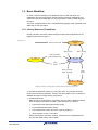
1.2 Basic Workflow
In order to perform rewriting of the data flash memory with the PFDL, the
initialization process for the library needs to be executed first. Afterwards, the
actual accesses to the data flash can be performed by means of dedicated API
functions.
The PFDL provides APIs for the C and assembly language of the CA78K0R, IAR,
GNU and CC-RL tool chains.
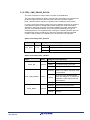
1.2.1 Library States and Transitions
During operation, the PFDL passes through several states as illustrated in the
diagram presented in Figure 1-1.
Figure 1-1
uninitialized/
closed
Reset or Power ON
PFDL_Open()
PFDL_Close()
PFDL_Execute()
(read command only)
busy (read)
opened
return
status
PFDL_Execute()
PFDL_Handler()
return
status
sequencer busy
State transition diagram of Data Flash Library Type 04
To operate the data flash memory by using the PFDL, the provided functions
need to be executed sequentially. Thereby, the library state can be controlled. A
detailed description of each state is given below:
1. uninitialized/closed
State at Power ON and Reset. In this state, the Pico FDL is disabled. Please
drive the library to this state via PFDL_Close whenever you want to
execute the Flash Self-programming Library,
run an EEPROM Emulation Library,
use a Data Flash Library other than Type 04 (PFDL), or
utilize a STOP or HALT command.
Please note that the execution of PFDL_Close has to be completed before
any of these listed actions can be taken.
R01US0055ED0112 Rev. 1.12
User Manual
10
2. opened
State in which the PFDL_Open function has been executed from the
uninitialized/closed state and the Data Flash Library is operational.
3. busy (read)
State in which the specified processing is being executed directly by the
library. The control does not return to the user program until the processing is
completed. Please note that the transition to this state is only triggered by the
read command in the PFDL.
4. sequencer busy
State in which the specified processing is being executed with the sequencer.
The PFDL_Execute function is used to trigger various commands to be
executed on the data flash memory and returns to the user program without
waiting for the completion of the sequencer operation. The current status of a
running operation in the sequencer can be checked and driven forward with
the PFDL_Hander function.
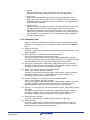
1.2.2 Exemplary Flow
Figure 1-2 shows an example of the data flash memory rewriting flow by using
the PFDL. In the following, a more detailed description is given of the illustrated
steps:
<1> Initializing the PFDL
The PFDL_Open function is called to initialize the RAM used for the PFDL and to
enable the library.
<2> Blank checking 1 to 1024 bytes for the specified address
(PFDL_CMD_BLANKCHECK_BYTES command)
The PFDL_Execute function (with the PFDL_CMD_BLANKCHECK_BYTES
command specified) is called to perform blank checking of 1 to 1024 bytes for the
specified address. The processing cannot be executed across blocks.
<3> Erasing the specified block (1 KB) (PFDL_CMD_ERASE_BLOCK command)
The PFDL_Execute function (with the PFDL_CMD_ERASE_BLOCK command
specified) is called to erase the specified block (1 KB).
<4> Writing 1 to 1024-byte data to the specified address
(PFDL_CMD_WRITE_BYTES command)
The PFDL_Execute function (with the PFDL_CMD_WRITE_BYTES command
specified) is called to write 1 to 1024 bytes to the specified address. The
processing cannot be executed across blocks.
<5> Internal verification of 1 to 1024 bytes for the specified address
(PFDL_CMD_IVERIFY_BYTES command)
The PFDL_Execute function (with the PFDL_CMD_IVERIFY_BYTES command
specified) is called to perform internal verification of 1 to 1024 bytes for the
specified address. The processing cannot be executed across blocks.
<6> Reading 1 to 1024 bytes from the specified address (PFDL_CMD_READ_BYTES
command)
The PFDL_Execute function (with the PFDL_CMD_READ_BYTES command
specified) is called to read 1 to 1024 bytes for the specified address. All the
processing of reading is executed within the PFDL_Execute function.
<7> Ending the PFDL operation
The PFDL_Close function is called to end the operation of the PFDL.
<8> Status checking
The PFDL_Handler function is called to perform status checking and drive a
running command. Status checking must be performed until the control to the
data flash memory by the sequencer is finished.
R01US0055ED0112 Rev. 1.12
User Manual
11
Figure 1-2
Begin of Data Flash control
<1>
<2>
PFDL_Open
PFDL_Execute
Note1
(BLANKCHECK command)
Error
Status check
Busy
<8>
PFDL_Handler
Busy
Blank check error
Status check
Normal completion
<3>
PFDL_Execute
(ERASE command)
Status check
Error
Busy
<8>
PFDL_Handler
Busy
Status check
Error
Normal completion
<4>
PFDL_Execute
(WRITE command)
Error
Status check
Busy
<8>
PFDL_Handler
Busy
Error
Status check
Normal completion
<5>
PFDL_Execute
(IVERIFY command)
Error
Status check
Busy
<8>
PFDL_Handler
Busy
Error
Status check
Normal completion
<6>
<7>
PFDL_Execute
(READ command)
PFDL_Close
End of Data Flash control
Exemplary flow of Data Flash operation using the PFDL
R01US0055ED0112 Rev. 1.12
User Manual
12
Note 1 Please note that the presented flow is only an example. It is not mandatory to
perform a blankcheck before an erase, if you are sure that you want to erase the
block in any case. The erase command performs an automatic blankcheck.
Please see Section 3.7.5 for details.
For a regular write however, please follow the suggested sequence of
blankcheck/write/iverify in order to ensure full data retention.
A detailed description of all PFDL API functions can be found in Section 3.6,
while all commands that can be triggered via PFDL_Execute are explained in
Section 3.7.
R01US0055ED0112 Rev. 1.12
User Manual
13
Chapter 2 Programming Environment
This chapter describes the hardware environment and software environment
required to rewrite the data flash memory using the Data Flash Library Type 04
(PFDL).
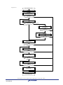
2.1 Hardware Environment
The PFDL for the RL78 microcontroller uses the sequencer to control the Data
Flash memory. As the sequencer has the direct control to the data flash memory,
the user program can be operated in parallel to the data flash memory control.
This is called BGO (background operation).
During rewriting of the data flash memory, the data flash memory is blocked for
other accesses. However, the code flash memory can be accessed, so interrupt
processing, the user program, and the PFDL can be allocated in the ROM for
operation as usual.
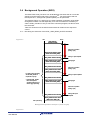
The access restrictions during data flash operations are depicted in Figure 2-1.
Figure 2-1
On-chip RAM
Data flash memory
The user program can operate
as usual with the BGO (background operation) during data
flash memory control.
×
Reading cannot be
executed during data
flash memory control.
Code flash memory
Interrupts can be used as
usual.
Access restrictions during Data Flash operation
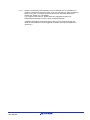
Figure 2-2 shows an example of execution of the Data Flash Library function to
perform rewriting of the data flash memory.
After an execution request has been send to the sequencer of the RL78
microcontroller via the PFDL API, the control is immediately returned to the user
program. For the current state and result of the issued FDL command, the status
check function (PFDL_Handler function) must be called repeatedly from the user
program. Please note that there are commands which require a calling
PFDL_Handler to drive the command execution (see Section 3.4 for details). The
actual number of handler calls required to finish a command is not predictable as
it depends on the type of command, the parameters and the time interval
between the calls.
R01US0055ED0112 Rev. 1.12
User Manual
14
Figure 2-2
User program
Pico FDL
Sequencer
PFDL_Execute
trigger
ongoing
busy
PFDL_Handler
trigger
ongoing
Segment in which the
Data Flash memory
cannot be referred to
busy
PFDL_Handler
trigger
finish
OK
Exemplary sequencer control via PFDL
2.1.1 Initialization
Before accessing the Data Flash memory by using the PFDL, the following
settings need to be performed:
1. Starting the high-speed on-chip oscillator
During the usage of the PFDL, keep the high-speed on-chip oscillator running.
When the oscillator is stopped, start the oscillator before using the PFDL.
2. Setting the CPU operating frequencyNote1
In order to perform the timing calculation used in the PFDL, set the CPU
operating frequency during the initialization. A detailed description of the
method that can be used to set the frequency can be found in Section 3.6.1
PDFL_Open.
3. Setting voltage modeNote2
In order to specify the voltage mode when writing the data flash memory,
select one of the following modes during the initialization.
Full-speed mode
Wide voltage mode
A detailed description of the method that can be used to set the voltage
mode can be found in Section 3.6.1 PDFL_Open.
R01US0055ED0112 Rev. 1.12
User Manual
15
Note 1 The CPU operating frequency is used for the parameters of the timing calculation
within the PFDL. The actual frequency of the processor core is not changed.
Note 2 For the details of the voltage mode, see the target RL78 microcontroller user's
manual.
2.1.2 Blocks
The flash memory of the RL78 microcontroller is divided into 1-KB blocks. In the
Data Flash Library, erasure processing is performed for the data flash memory in
the units of the blocks.
Reading, writing, blank checking or internal verification are performed on byte
granularity and require the specification of start addressNote and size.
Figure 2-3 shows an example of block positions and block numbers of the data
flash memory.
Note The address value is used when reading/writing data from/to the flash memory.
The address is specified relative to the first element of block 0 of the data flash
memory. Note that the specified address is not an absolute address.
Figure 2-3
Special function register SFR
General register
Internal high-speed RAM
Mirror
F17FFH
Data flash memory (2 KB)
F1000H
Not used
Special function register 2nd SFR
Not used
1 KB/2 blocks
07FFH
Code flash memory
User program
+
Flash data library
Data flash memory
Block 1
0400H
Data flash memory
Block 0
00000H
Absolute address
0000H
Relative address
Blocks of Data Flash Memory (here: RL78/G12 with 2 KB Data Flash)
R01US0055ED0112 Rev. 1.12
User Manual
16
2.2 Software Environment
The PFDL is allocated together with the program in the user area, occupying an
area equal to the size of the library. Furthermore, the library itself uses the CPU,
the stack, and a data buffer.
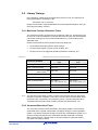
Detailed information about the required software resources is listed in Table 2-1.
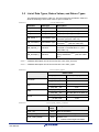
Resource consumptionNote1
Table 2-1
CA78K0R
IAR
GNU
CC-RL
Max code size
(program area)
175 bytes
180 bytes
199 bytes
168 bytes
Constants
(program area)
-
-
-
-
Internal data
-Note2
-Note2
-Note2
-Note2
Max. stack
consumption
46 bytes
46 bytes
50 bytes
40 bytes
Note1 All values for resource consumption are based on PFDL version V1.04.
Note2 Depending on the used device, the PFDL may use a fraction of the user RAM as
working area. Size and location of this area is strictly device dependent, see
Section 2.2.2 for more details.
2.2.1 File Structure
The actual file structure for the Data Flash Library T04 depends on the utilized
tool chain and is listed separately for CA78K0R, IAR, GNU and CC-RL in Table
2-2, Table 2-3 and Table 2-4, respectively.
Please note that assembler header files for GNU use the same extension ‘.h’ as
C header files, because the C preprocessor can and should be used for
assembler files in the GNU tool chain.
Table 2-2
File structure for CA78K0R tool chain
<root>
release.txt
Library release notes
<root>\lib
pfdl.h
PFDL interface definition (Compiler)
pfdl_types.h
PFDL types definition (Compiler)
pfdl.inc
PFDL interface definition (Assembler)
pfdl.lib
Pre-compiled library
<root>\smp
pfdl_sample_linker_file.dr
R01US0055ED0112 Rev. 1.12
User Manual
Sample linker file
17
Table 2-3
File structure for IAR tool chain
<root>
release.txt
Library release notes
<root>\lib
pfdl.h
PFDL interface definition (Compiler)
pfdl_types.h
PFDL types definition (Compiler)
pfdl.inc
PFDL interface definition (Assembler)
pfdl.r26
Pre-compiled library
<root>\smp
pfdl_sample_linker_file.xcl
Sample linker file
File structure for GNU tool chain
Table 2-4
<root>
release.txt
Library release notes
<root>\lib
pfdl.h
PFDL interface definition (Compiler)
pfdl_types.h
PFDL types definition (Compiler)
pfdl_asm.h
PFDL interface definition (Assembler)
pfdl.a
Pre-compiled library
<root>\smp
pfdl_sample_linker_file.ld
Sample linker file
File structure for CC-RL tool chain
Table 2-5
<root>
release.txt
Library release notes
<root>\lib
pfdl.h
PFDL interface definition (Compiler)
pfdl_types.h
PFDL types definition (Compiler)
pfdl.inc
PFDL interface definition (Assembler)
pfdl.lib
Pre-compiled library
<root>\smp
pfdl_sample_linker_file.sub
R01US0055ED0112 Rev. 1.12
User Manual
Sample linker file
18
2.2.2 Prohibited RAM Area
The PFDL may use a fraction of the user RAM as working area, referred as
prohibited RAM area. The size and position of this area is strictly device
dependent (many devices do not even have this area) and vary between the
different RL78 products. For details, please refer to the document "User’s
Manual: Hardware" of your RL78 product.
If a prohibited RAM area is specified for the utilized device, it is not allowed to
access this area while the PFDL is active. Whenever PFDL functions are called,
the data in the prohibited area may be rewritten.
2.2.3 Register Bank
The CA78K0R, IAR and CC-RL releases of the PFDL use the registers of the
currently selected register bank. No implicit register bank switch is performed by
the library.
For the GNU release of the PFDL, it is mandatory that register bank 0 is active on
function entry. No implicit register bank switch is performed by the library. Return
values are placed in register bank 1. For details on GNU calling conventions,
please refer to the GNU documentation for RL78 devices.
Remark A detailed description of the registers used for parameter passing and return
values can be found in Section 3.6 Description of Data Flash Library Functions.
2.2.4 Stack and Data Buffer
The PFDL uses the sequencer to write to the code flash memory, but it uses the
CPU for pre-setting and control. Therefore, the PFDL also utilizes the stack
specified by the user program.
Remark To allocate the stack and data buffer to the user-specified address, the link
directive is used.
Stack
In addition to the stack used by the user program, the stack space required
for flash functions must be reserved in advance. It has to be ensured that the
stack is allocated so that the RAM used by the user will not be destroyed
during stack processing of the PFDL. The stack may not be allocated in the
short address range from FFE20H to FFEFFH—and also not in the prohibited
RAM area, if it exists in the target device.
For the actual stack space required for the Data Flash Library functions,
please refer to Table 2-1.
Data buffer
The usage of the data buffer is described in following:
Work area for internal processing of the PFDL
RAM area in which data is located that is to be written into the data flash
RAM area in which data is located that is to be obtained from the data
flash
The data buffer may not be allocated in the short address range from
FFE20H to FFEFFH—and also not in the prohibited RAM area, if it exists in
the target device.
Please note that the allocation and usage of the data buffer falls into the
responsibility of the user. Especially it has to be ensured that the data buffer
is not touched by any other part of the user application while a read or write
command accessing this buffer is still running.
R01US0055ED0112 Rev. 1.12
User Manual
19
2.2.5 Data Flash Library
Not all Data Flash Library functions are linked. Only the really utilized Data Flash
Library functions are linkedNote.
Memory allocation of the PFDL
Segments are assigned to the functions and variables used in the PFDL. The
used areas of the PFDL can be mapped to specific locations.
For details, refer to 3.2 Segments of Data Flash Library Functions.
Note For the CA78K0R and CC-RL assembler, linking can be reduced to a subset of
the Data Flash Library functions by deleting unnecessary functions from the
include file.
2.2.6 Program Area
This is the area in which the PFDL and the user program using the PFDL are
located.
Utilizing the PFDL for the RL78 microcontroller, the user program can be
operated during rewriting of the Data Flash memory, because the Data Flash
memory is controlled by the sequencer in the background (background operation).
For details, refer to the sections of Chapter 3 Data Flash Library Function.
2.2.7 Using the PFDL on the R5F10266 device
For the R5F10266 device, RAM is a scarce resource. The device comes with 256
bytes RAM which cannot be used completely by the PFDL. Hence special care
has to be taken for a proper RAM usage by a dedicated linking method.
Note Due to the limited memory resource—especially for the stack—the usage of
interrupts is prohibited for the R5F10266 device when the PFDL is used.
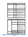
Table 2-6 shows the usage for the different RAM areas on the R5F10266 device
when using the PFDL.
RAM usage for R5F10266 when using PFDL
Table 2-6
Address
range
Size
(byte)
Description
Usage and Limitations
Free area
Please allocate your PFDL function
arguments, and data buffers in this area.
Short-address
area
Do not allocate any PFDL function
argument, data buffer or stack in this
area.
0xFFE00 –
0xFFE1F
32
0xFFE20 –
0xFFEA1
130
0xFFEA2 –
0xFFEDF
62
Stack allocation
area
Please allocate the stack into this area
when using R5F10266.
Please ensure that the stack does not
exceed this area (including library and
user application, see also Table 2-1).
0xFFEE0 –
0xFFEFF
32
General-purpose
register area
Do not allocate any PFDL function
argument, data buffer or stack in this
area.
R01US0055ED0112 Rev. 1.12
User Manual
20
2.3 Cautions on the Programming Environment
1.
Library code must be located completely in the same 64k flash page.
2.
The PFDL library initialization by PFDL_Open must be performed before the
execution of PFDL_Close, PFDL_Execute, PFDL_Handler.
3.
It is not allowed to read the data flash during a command execution of the
PFDL.
4.
It is not possible to modify the Data Flash in parallel to a modification of the
Code Flash.
5.
Do not execute the Flash Self-programming Library, EEPROM Emulation
Library, or Data Flash Library other than Type 04 during the execution of the
PFDL. When using the Flash Self-programming Library, EEPROM Emulation
Library, or Data Flash Library other than Type 04, be sure to execute
PFDL_Close to close the PFDL.
6.
Do not execute the STOP command mode or HALT command mode during
the execution of the PFDL. If the STOP command or HALT command needs
to be executed, be sure to execute the PFDL_Close function to close the
PFDL.
7.
The watchdog timer does not stop during the execution of the PFDL.
8.
Do not allocate any PFDL function argument, data buffer or stack used by
the Data Flash Library to an address over 0xFFE20 or in the prohibited RAM
area (if existent for your target device).
9.
When using the data transfer controller (DTC) during the execution of the
PFDL, do not allocate the RAM area used by the DTC to an address over
0xFFE20 or in the prohibited RAM area (if existent for your target device).
10. Do not use the RAM area (including the prohibited RAM area) used by the
PFDL until the library is closed.
11. Do not execute a Data Flash Library function within interrupt processing
because the PFDL does not support multiple executions of a Data Flash
Library function.
12. When executing the PFDL within an operating system, do not execute a
Data Flash Library function from multiple tasks, because the PFDL does not
support multiple executions of a Data Flash Library function.
13. Before initiating any operation with the PFDL, the high-speed on-chip
oscillator needs to be started.
14. Note the following regarding the operating frequency of the RL78
microcontroller and the operating frequency value set with the initialization
function (PFDL_Open).
When a frequency below 4 MHzNote1 is used as the operating frequency
of the RL78 microcontroller, 1 MHz, 2 MHz, or 3 MHz can be used (a
frequency such as 1.5 MHz that is not an integer value cannot be used).
Also, set an integer value such as 1, 2, or 3 as the operating frequency
value set with the initialization function.
When a frequency over 4 MHzNote1 is used as the operating frequency of
the RL78 microcontroller, a frequency with decimal places can be used.
However, specify a rounded up integer value as the operating frequency
set with the initialization function (PFDL_Open).
Example: For 4.5 MHz, set "5" with the initialization function.
The operating frequency is not the frequency of the high-speed on-chip
oscillator.
15. The PFDL does not perform error checking of the parameters set in the
argument of a Data Flash Library function. Therefore, make sure to set a
R01US0055ED0112 Rev. 1.12
User Manual
21
correct value to the parameter after checking the specifications of the target
RL78 microcontroller. If parameter checking is required to set a correct value,
perform it in the user program.
16. Please initialize all function arguments (including unused structure elements)
at least once before calling a function. Otherwise, a RAM parity error may
cause a reset of the device. For details, please refer to the document "User's
Manual: Hardware" of your RL78 product.
17. Do not write to a data flash cell that is not erased. It is prohibited to rewrite a
data flash cell without erasing the corresponding data flash block first. The
PFDL does not contain any sanity checks to prevent such a situation. The
user is responsible to ensure the compliance of this rule.
18. The data flash control register (DFLCTL) should not be operated during the
execution of the PFDL. In addition, when the operation of the PFDL is ended,
the DFLCTL is set to access inhibit state by the PFDL_Close function.
If accessing the data flash memory is required even after the operation of the
PFDL is ended, verify the completion of the PFDL_Close function, set the
DFLCTL to the access permit state and perform the setupNote2.
19. After the execution of PFDL_Close, all requested/running commands will be
aborted and cannot be resumed. The user has to take care that all running
commands are finished before calling PFDL_Close.
Note 1 For the range of the operating frequency, see the target RL78 microcontroller
user’s manual.
Note 2 For the method of the setup, see the target RL78 microcontroller user’s manual.
R01US0055ED0112 Rev. 1.12
User Manual
22
Chapter 3 Data Flash Library Function
This chapter describes the details of the Data Flash Library functions.
3.1 Type of Data Flash Library Functions
The PFDL provides the following flash functions as listed in Table 3-1.
Table 3-1
List of Data Flash Library functions
Function name
Description
PFDL_Open
Initialization of the RAM used by the PFDL, enabling of the
Data Flash clock
PFDL_Close
Ending the operation of the PFD, disabling of the Data
Flash clock
PFDL_Execute
Triggering and execution of commands on the Data Flash
memory
PFDL_Handler
Checking of the current status of a running Data Flash
operation and driving the command forward
(status check processing)
PFDL_GetVersionString
Acquisition of the version information of the PFDL
3.2 Segments of Data Flash Library Functions
The Data Flash Library functions are located in the following segment:
PFDL_COD:
Segment of the Data Flash Library functions.
It can be allocated to the ROM or RAM.
3.3 Commands
All flash operations are issued in the PFDL via the PFDL_Execute function. The
command specified as argument of PFDL_Execute determines the type of the
flash operation. Table 3-2 lists all available commands. For details on the
execution method, please refer to Section 3.6.3.
Table 3-2
List of commands specified for PFDL_Execute (pfdl_command_t)
Definition
Value
Command name
PFDL_CMD_READ_BYTES
0x00
Read command
PFDL_CMD_BLANKCHECK_BYTES
0x08
Blank check command
PFDL_CMD_ERASE_BLOCK
0x03
Erasure command
PFDL_CMD_WRITE_BYTES
0x04
Write command
PFDL_CMD_IVERIFY_BYTES
0x06
Internal verification command
R01US0055ED0112 Rev. 1.12
User Manual
23
3.4 Background Operation (BGO)
The Data Flash Library functions can be divided into functions that do not use the
sequencer and functions that use the sequencerNote. For the functions that use
the sequencerNote, background operation (BGO) can be performed.
The following Figure 3-1 and Figure 3-2 show examples of operation of the PFDL
during BGO. Please note that especially for a write command it is mandatory to
call the PFDL_Handler not only to check the command progress, but also to drive
the command.
Table 3-3 shows a list of the API functions with their relation to the sequencer
control.
Note Not during the execution of the PFDL_CMD_READ_BYTES command.
Figure 3-1
User
Library
PFDL_Execute
function executed
Sequencer in operation
(Writing 1 byte)
PFDL_Execute function closed
(Return value: PFDL_BUSY)
PFDL_Handler function executed
PFDL_Handler function closed
(Return value: PFDL_BUSY)
PFDL_Handler function executed
Writing of 1 byte completed
Writing trigger
Sequencer in operation
(Writing 1 byte)
PFDL_Handler function closed
(Return value: PFDL_BUSY)
For writing, trigger processing
with the PFDL_Handler is
required for every byte.
Writing of 2 bytes completed
PFDL_Handler function executed
* Executing PFDL_Handler
before the sequencer
completes writing does not
result in trigger processing.
PFDL_Handler function closed
(Return value: PFDL_BUSY)
Writing trigger
Sequencer in operation
(Writing 1 byte)
PFDL_Handler function executed
Writing of all 3 bytes
completed
PFDL_Handler function closed
(Return value: PFDL_OK)
End of processing
Background operation example 1 (write: 3 byte)
Figure 3-2
R01US0055ED0112 Rev. 1.12
User Manual
24
User
Library
PFDL_Execute function
executed
PFDL_Execute function closed
(Return value: PFDL_BUSY)
PFDL_Handler function executed
The control returns immediately, so
other processing can be executed.
The state must be checked until the
completion.
* Not during the execution of the
PFDL_CMD_READ_BYTES
command.
Sequencer in operation
PFDL_Handler function closed
(Return value: PFDL_BUSY)
PFDL_Handler function executed
PFDL_Handler function closed
(Return value: PFDL_OK)
End of processing
Background operation example 2 (erase, iverify, blankcheck)
Table 3-3
List of interrupt reception and BGO of Data Flash Library functions
Function name
PFDL_Open
PFDL_Close
PFDL_Execute
PFDL_Handler
PFDL_GetVersionString
Sequencer control /
BGO function
Interrupt reception
No
YesNote
Allowed
No
Note Not during the execution of the PFDL_CMD_READ_BYTES command.
R01US0055ED0112 Rev. 1.12
User Manual
25
3.5 List of Data Types, Return Values, and Return Types
The data types are listed in Table 3-4. The return types are specified in Table 3-5,
while the meaning of each return value is given in Table 3-6.
Table 3-4
List of data types
Definition
Data type
Description
pfdl_u08
unsigned char
1-byte (8-bit) unsigned integer
pfdl_u16
unsigned int
2-byte (16-bit) unsigned integer
pfdl_u32
unsigned long int
4-byte (32-bit) unsigned integer
pfdl_status_t
enumeration type
set of 1-byte (8-bit) unsigned integer
constants (see also Table 3-6)
pfdl_command_t
enumeration type
set of 1-byte (8-bit) unsigned integer
constants Note 1 (see also Table 3-2)
pfdl_request_t
structure
structure to specify requests to be
executed on the data flash Note 1 (see
also Table 3-7)
pfdl_descriptor_t
structure
structure to specify the configuration for
library initialization Note 2 (see also Table
3-7)
Note 1 A detailed description can be found in Section 3.6.3 PFDL_Execute.
Note 2 A detailed description can be found in Section 3.6.1 PDFL_Open.
List of return types
Table 3-5
Return value
C language
CA78K0R
IAR
GNU
CC-RL
Table 3-6
Assembly language
pfdl_status_t
C
__far pfdl_u08*
DE:BC
pfdl_status_t
A
pfdl_u08 __far*
A:HL
pfdl_status_t
R8 (X on bank 1)
pfdl_u08 __far*
R11:R8 (BC:AX on bank 1)
pfdl_status_t
A
__far pfdl_u08*
A:DE
List of pfdl_status_t values
Definition
Return
value
Description
PFDL_OK
0x00
Normal completion
PFDL_ERR_PROTECTION
0x10
Reserved for future usage
PFDL_ERR_ERASE
0x1A
Erasure error
R01US0055ED0112 Rev. 1.12
User Manual
Erasure of the target area failed.
26
Definition
Return
value
PFDL_ERR_MARGIN
PFDL_ERR_WRITE
0x1B
0x1C
Description
Blank check error or Internal verification
error
The target area is not in the blank
state.
An error occurred during internal
verification processing of the target
area.
Writing error
PFDL_IDLE
0x30
Idle state
PFDL_BUSY
0xFF
Other
than
above
Table 3-7
No command is executed in the
PFDL_Execute function.
Execution start of the PFDL_Execute
function command, or in execution
Other than above
Writing to the target area failed.
The command specified in the
PFDL_Execute function is in
execution.
Other error
An abnormal return value. Check
the specified command or resource
allocation again.
List of structures
Structure
Member
Description
pfdl_u16 index_u16
Target area
Erasure: block number
Other: start address of the
target area
pfdl_u08* data_pu08
(near)
Pointer to the data buffer for
acquisition of data to be written or
read. Only used for read/write
commands
pfdl_u16 bytecount_u16
Number of bytes to be transferred
starting from the start byte
specified in index_u16. The byte
count range is from 1 byte to 1024
bytes. Please note, that the
execution of the
read/write/blankcheck/internal
verify command across block
boundaries is not allowed. This
struct member is not required for
the erase command.
pfdl_command_t
command_enu
Command to be executed
pfdl_u08 fx_MHz_u08
CPU frequency
pfdl_u08
wide_voltage_mode_u08
Voltage mode setting
pfdl_request_t
pfdl_descriptor_t
R01US0055ED0112 Rev. 1.12
User Manual
27
3.6 Description of Data Flash Library Functions
The flash functions are described in the following format.
Outline Describes the purpose of the function.
Interface Describes the C interfaces and assembler labels required to access the function.
Arguments Describes the parameters, return values and register usage of the function.
Precondition Describes the conditions that have to be fulfilled before calling the function.
Description Describes the function details and cautions of this function.
R01US0055ED0112 Rev. 1.12
User Manual
28
3.6.1 PDFL_Open
Outline Initialization of all internal data and activation of the data flash.
Interface C interface for CA78K0R compiler
pfdl_status_t __far PFDL_Open(__near pfdl_descriptor_t*
descriptor_pstr);
C interface for IAR compiler
__far_func pfdl_status_t PFDL_Open(__near pfdl_descriptor_t
__near* descriptor_pstr);
C interface for GNU compiler
pfdl_status_t PFDL_Open(pfdl_descriptor_t* descriptor_pstr)
__attribute__ ((section ("PFDL_COD")));
C interface for CC-RL compiler
pfdl_status_t __far PFDL_Open(__near pfdl_descriptor_t*
descriptor_pstr);
ASM function label for CA78K0R, IAR, GNU and CC-RL assembler
PFDL_Open
Arguments Parameters
Registers
Argument
Type
Description
CA78K0R
descriptor_pstr
pfdl_desc
riptor_t*
(near)
AX
IAR
AX
GNU
stack
CC-RL
AX
address of the
descriptor variable
located in the RAM,
defines voltage
mode and CPU
frequency
Structures
Structure
pfdl_descriptor_t
R01US0055ED0112 Rev. 1.12
User Manual
Member
Description
pfdl_u08 fx_MHz_u08
CPU frequency
pfdl_u08 wide_voltage_mode_u08
Voltage mode setting
29
Return value
Registers
Type
pfdl_status_t
Description
CA78K0R
IAR
GNU
CC-RL
C
A
R8
(X bank 1)
A
Status of operation,
PFDL_OK (only possible
value)
Destructed registers
Tool chain
Destructed registers
CA78K0R
AX
IAR
X
GNU
none
CC-RL
X, HL, C
Preconditions The following conditions need to be ensured before using PFDL_Open
The Flash Self-programming Library, the EEPROM Emulation Library, or any
Data Flash Library other than Type 04 are not running or have been closed.
The high-speed on-chip oscillator is running.
Description By calling PFDL_Open, the Data Flash Library is put into operational state and
the data flash of the RL78 device is activated.
PFDL_Open reserves and initializes the prohibited RAM areaNote 1 used for the
PFDL. If a prohibited RAM areaNote 1 exists, do not use it until the PFDL is closed.
For correct operation, the voltage modeNote 2 of the PFDL needs to be specified in
the wide_voltage_mode_u08 structure member of the argument
pfdl_descriptor_t:
00H: Full-speed mode
01H: Wide voltage mode
Furthermore, the operating frequency of the CPU needs to be set in the
fx_MHz_u08 structure member of the argument pfdl_descriptor_t. This parameter
is used for the calculation of timing data in the PFDLNote 3. For the value of the
operating frequency of the CPU (fx_MHz_u08), note the following:
When a frequency below 4 MHzNote 4 is used as the operating frequency of
the RL78 microcontroller, only integer frequencies (1 MHz, 2 MHz, or 3 MHz)
can be used. Frequencies with decimal fraction (e.g. 1.5 MHz) are not
supported. The value of fx_MHz_u08 has to match the actual operating
frequency of the device.
When a frequency over 4 MHzNote 4 is used as the operating frequency of the
RL78 microcontroller, a frequency with decimal franction can be used.
However, the fx_MHz_u08 parameter for PFDL_Open needs to be set to the
corresponding rounded up integer in this case.
(Example: For 4.5 MHz, set a value of “5” with the initialization function.)
The operating frequency is not the frequency of the high-speed on-chip
oscillator.
R01US0055ED0112 Rev. 1.12
User Manual
30
Note 1 For the prohibited RAM area, refer to the document “User’s Manual: Hardware” of
your target RL78 microcontroller.
Note 2 For details of the voltage mode, refer to the user’s manual of the target RL78
microcontroller.
Note 3 It is a required parameter for timing calculation in the Flash Self-programming
Library. This setting does not change the operating frequency of the RL78
microcontroller.
Note 4 For the range of the maximum operating frequency, refer to the document “User’s
Manual: Hardware” of your target RL78 microcontroller.
R01US0055ED0112 Rev. 1.12
User Manual
31
3.6.2 PFDL_Close
Outline Ends the operation of the Data Flash Library and drives it into closed state.
Interface C interface for CA78K0R compiler
void __far PFDL_Close(void);
C interface for IAR compiler
__far_func
void
PFDL_Close(void);
C interface for GNU compiler
void
PFDL_Close(void) __attribute__ ((section ("PFDL_COD")));
C interface for CC-RL compiler
void __far PFDL_Close(void);
ASM function label for CA78K0R, IAR, GNU and CC-RL assembler
PFDL_Close
Arguments no parameters, no return value
Destructed registers
Tool chain
Destructed registers
CA78K0R
none
IAR
none
GNU
none
CC-RL
C
Preconditions Before the execution of this function, the PFDL_Open function must have been
completed normally.
Furthermore, all running commands have to be finished before calling
PFDL_Close.
R01US0055ED0112 Rev. 1.12
User Manual
32
Description The function PFDL_Close ends the operation of the Data Flash Library and
disables the data flash memory. Please call PFDL_Close whenever you want to
execute the Flash Self-programming Library,
run an EEPROM Emulation Library,
use a Data Flash Library other than Type 04, or
utilize a STOP or HALT command.
Please note that the execution of PFDL_Close has to be completed before any of
these listed actions can be taken.
R01US0055ED0112 Rev. 1.12
User Manual
33
3.6.3 PFDL_Execute
Outline Executes control commands on the data flash memory.
Interface C interface for CA78K0R compiler
pfdl_status_t __far PFDL_Execute(__near pfdl_request_t*
request_pstr);
C interface for IAR compiler
__far_func
pfdl_status_t
PFDL_Execute(__near pfdl_request_t
__near* request_pstr);
C interface for GNU compiler
pfdl_status_t
PFDL_Execute(pfdl_request_t* request_pstr)
__attribute__ ((section ("PFDL_COD")));
C interface for CC-RL compiler
pfdl_status_t __far PFDL_Execute(__near pfdl_request_t*
request_pstr);
ASM function label for CA78K0R, IAR, GNU and CC-RL assembler
PFDL_Execute
Arguments Parameters
Registers
Argument
Type
Description
CA78K0R
request_pstr
R01US0055ED0112 Rev. 1.12
User Manual
pfdl_reques
t_t* (near)
AX
IAR
AX
GNU
stack
CC-RL
AX
Address of the
structure specifying
the flash command
to be executed
34
Structures
Structure
Member
Description
pfdl_u16 index_u16
Target area
Erasure: block number
Other: start addressNote 2 of the
target area
Pointer to the data buffer for
acquisition of data to be written or
readNote1
pfdl_u08* data_pu08
(near)
pfdl_request_t
Only used for read/write commands
Range of the command specified in
bytesNote1 (starting from the specified
start addressNote 2)
pfdl_u16 bytecount_u16
Not required for erase commands
pfdl_command_t
command_enu
Command to be executed
Note 1 Specify only for commands requiring the target parameter (if not required,
initialize with arbitrary value). The byte count range is from 1 byte to 1024 bytes.
Provide the data buffer size for the number of bytes of the data to be written or
read. Please note that the specified range may not cross block and has to be
specified within one block.
Note 2 The specified address is the relative address that starts from block 0 of data flash
memory as address 0. This is not the absolute address.
Figure 3-3 Absolute address
Relative address
F1FFFH
0FFFH
Block 3
Address to be specified
when using the PFDL
Block 2
Block 1
Block 0
F1000H
0000H
Address specification for commands executed via PFDL_Execute
Return value
Registers
Type
pfdl_status_t
R01US0055ED0112 Rev. 1.12
User Manual
Description
CA78K0R
IAR
GNU
CC-RL
C
A
R8
(X bank 1)
A
Status of operation, can
be PFDL_BUSY or
PFDL_OK
35
Destructed registers
Tool chain
Destructed registers
CA78K0R
AX
IAR
X
GNU
none
CC-RL
X, BC, DE, HL
Preconditions Before the execution of this function, the PFDL_Open function must be
completed normally.
Furthermore, a running command must be finished (via PFDL_Handler) before it
is allowed to call PFDL_Execute again.
Although it depends on the command which members of the request structure
are necessary for the execution (see Table 3-8), all members of the request
variable must be initialized. If there are any unused members in the request
variable, the user has to set arbitrary values to these members.
Description The PFDL_Execute function triggers the execution of the specified command on
the data flash memory. The available commands are listed in Table 3-8. Please
note that – except the read command – all commands are propagated to the
sequencer and executed in the background. The final status of the execution
needs to be checked via FDL_Handler. A more detailed description of each
command can be found in Section 3.7 Description of Data Flash Library
Commands.
Table 3-8
List of Execution Commands (pfdl_command_t)
Command
Value
Description
Reads the specified number of bytes from the
specified starting addressNote2 in the data flash
memory and places it in the read data input buffer.
The following arguments must be set for execution:
PFDL_CMD_READ_BYTES
0x00
pfdl_request_t.index_u16:
Reading start addressNote2
pfdl_request_t.bytecount_u16:
Read size
pfdl_request_t.data_pu08:
Address of the read data input buffer
Performs blank checking from the specified
beginning addressNote2 of the data flash memory for
the area in the execution range.
The following arguments are usedNote3:
PFDL_CMD_BLANKCHECK_BYTES
PFDL_CMD_ERASE_BLOCK
0x08
0x03
pfdl_request_t.index_u16:
Start addressNote2
pfdl_request_t.bytecount_u16:
Execution range from the start
addressNote1
Performs erasure for the block of the specified
number in the data flash memory.
The following arguments are usedNote3:
R01US0055ED0112 Rev. 1.12
User Manual
pfdl_request_t.index_u16:
Block number
36
Command
Value
Description
Writes the data placed in the write data input buffer
to the data flash memory at the specified starting
addressNote2 for the specified number of bytes.
The following arguments must be set for execution:
PFDL_CMD_WRITE_BYTES
0x04
pfdl_request_t.index_u16:
Write start addressNote2
pfdl_request_t.bytecount_u16:
Write sizeNote1
pfdl_request_t.data_pu0:
Address of the write data input buffer
Performs internal verification starting from the
specified beginning addressNote2 of the data flash
memory for the area in the execution range.
The following arguments are usedNote3:
PFDL_CMD_IVERIFY_BYTES
0x06
pfdl_request_t.index_u16:
Start addressNote2
pfdl_request_t.bytecount_u16:
Execution range from the start
addressNote1
Note 1 Cannot be specified across blocks. Specify it within one block.
Note 2 The specified address is the relative address that starts from block 0 of the data
flash memory as address 0 when writing and reading the memory. Note that the
specified address isn’t an absolute address.
Note 3 All members of the request variable must be initialized. Unused members in the
request variable can be set to arbitrary values.
R01US0055ED0112 Rev. 1.12
User Manual
37
3.6.4 PFDL_Handler
Outline Checking of the current processing state of a previously issued command and
driving the command forward (especially in case of a write command).
Interface C interface for CA78K0R compiler
pfdl_status_t __far PFDL_Handler(void);
C interface for IAR compiler
__far_func
pfdl_status_t PFDL_Handler(void);
C interface for GNU compiler
pfdl_status_t
PFDL_Handler(void)
__attribute__ ((section ("PFDL_COD")));
C interface for CC-RL compiler
pfdl_status_t __far PFDL_Handler(void);
ASM function label for CA78K0R, IAR, GNU and CC-RL assembler
PFDL_Handler
Arguments Parameters
none
Return value
Registers
Type
Description
CA78K0R
pfdl_status_t
R01US0055ED0112 Rev. 1.12
User Manual
C
IAR
A
GNU
R8
(X bank 1)
CC-RL
A
Status of operation,
can be PFDL_BUSY,
PFDL_OK, PFDL_IDLE,
PFDL_ERR_MARGIN,
PFDL_ERR_WRITE or
PFDL_ERR_ERASE
38
Destructed registers
Tool chain
Destructed registers
CA78K0R
none
IAR
none
GNU
none
CC-RL
C
Precondition Before the execution of this function, the PFDL_Open function must be
completed normally.
Description Checks the control state of the command specified in the PFDL_Execute function
executed beforehand and performs required settings for continuous execution.
While the status is PFDL_BUSY, the running command is not finished yet and
new commands may not be issued. PFDL_OK indicates the successful
completion of a command.
The possible error codes depend on the type of the triggered command. Please
refer to the individual command descriptions in Section 3.7 Description of Data
Flash Library Commands.
R01US0055ED0112 Rev. 1.12
User Manual
39
3.6.5 PFDL_GetVersionString
Outline Acquisition of the version information of the PFDL.
Interface C interface for CA78K0R compiler
__far pfdl_u08* __far PFDL_GetVersionString(void);
C interface for IAR compiler
__far_func pfdl_u08 __far* PFDL_GetVersionString(void);
C interface for GNU compiler
pfdl_u08 __far* PFDL_GetVersionString(void)
__attribute__ ((section ("PFDL_COD")));
C interface for CC-RL compiler
__far pfdl_u08* __far PFDL_GetVersionString(void);
ASM function label for CA78K0R, IAR, GNU and CC-RL assembler
PFDL_GetVersionString
Arguments Parameters
none
Return value
Registers
Type
Description
CA78K0R
pfdl_u08*
(far)
DE:BC
IAR
GNU
A:HL
R11..R8
(BC:AX
bank 1)
CC-RL
A:DE
Beginning address (24 bit) of the
area where the version
information of the PFDL is
stored as 0-terminated ASCII
string.
Destructed registers
none
R01US0055ED0112 Rev. 1.12
User Manual
40
Preconditions none
Description The function PFDL_GetVersionString can be used to obtain the version
information of the utilized library. The version string is given in the following
format:
DRL78T04cxx..xyabc
where
c codes the target compiler for the used library,
“R” for CA78K0R, “I” for IAR, “U” for GNU and “L” for CC-RL
xx..x codes the information about the used compiler version and memory
model (the length can be between 4 and 5 digits depending on the compiler
and release date of the library),
y identifies the release type, “V” for release, “E” for engineering version,
abc specifies the library version as Va.bc .
R01US0055ED0112 Rev. 1.12
User Manual
41
3.7 Description of Data Flash Library Commands
The PFDL offers a set of commands that all can be requested by using the
PFDL_Execute function.
Note All commands operate on virtual addresses (relative address that starts from
block 0 of the data flash memory as address 0) and block numbers.
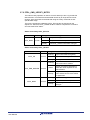
3.7.1 PFDL_CMD_READ_BYTES
The read command is used to read a number of bytes from data flash. It is the
only command that does not need the sequencer. It is initiated and finished
directly by PFDL_Execute.
Status returned by PFDL_Execute
Status
PFDL_OK
R01US0055ED0112 Rev. 1.12
User Manual
Class
normal
Background and Handling
meaning
request was finished regularly
reason
no problems during command execution
occurred
remedy
nothing
42
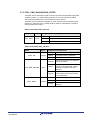
3.7.2 PFDL_CMD_IVERIFY_BYTES
The internal verify operation is used to check if all bits (0’s and 1’s) provide full
data retention. Inconsistent and weak data caused by an asynchronous reset
during a write command can be detected using the iverify command on that
specific data range.
The iverify command is initiated by PFDL_Execute and is executed by the
sequencer. After that, PFDL_Handler shall be called to complete the command
and check the PFDL status.
Status returned by PFDL_Execute
Status
PFDL_BUSY
Class
normal
Background and Handling
meaning
request is being processed
reason
request has been accepted
remedy
call PFDL_Handler until status changes
Status returned by PFDL_Handler
Status
PFDL_OK
PFDL_ERR_MARGIN
PFDL_BUSY
R01US0055ED0112 Rev. 1.12
User Manual
Class
normal
normal
normal
Background and Handling
meaning
request was finished regularly
reason
no problems during execution
remedy
nothing
meaning
at least one bit within the specified
area could not be verified
reason
margin for internal verification is
below the value required for full
data retention
remedy
no general remedy, the requester
has to decide how to react based
on application
meaning
request is being processed
reason
request has been accepted
remedy
call PFDL_Handler until status
changes
43
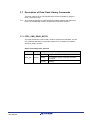
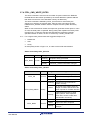
3.7.3 PFDL_CMD_BLANKCHECK_BYTES
The blank-check command is used to check if all cells in the specified target flash
area are “erased”, e.g. before writing data into it. The user can use the blankcheck command freely as it is a non-destructive flash access.
The blank-check command is initiated by PFDL_Execute and is executed by the
sequencer. After that, PFDL_Handler shall be called to complete the command
and check the PFDL status.
Status returned by PFDL_Execute
Status
PFDL_BUSY
Class
normal
Background and Handling
meaning
request is being processed
reason
request has been accepted
remedy
call PFDL_Handler until status changes
Status returned by PFDL_Handler
Status
PFDL_OK
PFDL_ERR_MARGIN
PFDL_BUSY
R01US0055ED0112 Rev. 1.12
User Manual
Class
normal
light
normal
Background and Handling
meaning
request was finished regularly
reason
no problems during execution
remedy
nothing
meaning
at least one bit within the specified
area is not blank
reason
for any bit of the checked area, the
margin for an erased cell is below
the value required for full data
retention
remedy
no general remedy, the requester
has to decide how to react based
on the application
meaning
request is being processed
reason
request has been accepted
remedy
call PFDL_Handler until status
changes
44
3.7.4 PFDL_CMD_WRITE_BYTES
The write command is used to write a number of bytes located in the RAM into
the data flash at the location specified by the virtual addresses (relative address
that starts from block 0 of the data flash memory as address 0).
The write command is initiated by PFDL_Execute and is executed by the
sequencer to perform the physical write. After the write command has been
initiated PFDL_Handler shall be called to complete it and to update the library
status.
When a write command is issued, the sequencer generates a write-pulse. In case
of a fail, the write pulse is repeated. During write-pulse repetition the library state
remains busy. In case the write process fails after the maximum internally
specified number of retries, an error is returned by a PFDL_Handler call.
Note For a regular write, please follow the suggested sequence of
blankcheck
write
iverify
as exemplarily shown in Figure 1-2, in order to ensure full data retention.
Status returned by PFDL_Execute
Status
PFDL_BUSY
Class
normal
Background and Handling
meaning
request is being processed
reason
request has been accepted
remedy
call PFDL_Handler until status changes
Status returned by PFDL_Handler
Status
PFDL_OK
PFDL_ERR_WRITE
PFDL_BUSY
R01US0055ED0112 Rev. 1.12
User Manual
Class
normal
Background and Handling
meaning
request was finished regularly
reason
no problems during execution
remedy
nothing
meaning
at least one byte could not be
written correctly
reason
for any bit of the written area, the
margin for written data is below the
value required for full data retention
remedy
erase the block and try to write
again (caution: erase operates
block-wise, ensure to safe other
data stored in the block)
meaning
request is being processed
reason
request has been accepted
remedy
call PFDL_Handler until status
changes
heavy
normal
45
3.7.5 PFDL_CMD_ERASE_BLOCK
The erase command is used to erase one block of the data flash.
The command is initiated by PFDL_Execute and is executed by the sequencer to
perform the physical erase. After the erase command has been initiated
PFDL_Handler shall be called to complete it and to update the library status.
In order to avoid unnecessary erase cycles, the hardware sequencer is checking
if the addressed block is already blank before starting the actual erase-pulse
generation. After that, the erase-command is initiated and finally a block blankcheck is executed automatically. This is repeated automatically as long the
addressed block is not completely blank. During the complete repetition process
the Data Flash Library remains busy. When the maximum internally specified
number of erase retries is exceeded an error is returned to the requester.
Status returned by PFDL_Execute
Status
PFDL_BUSY
Class
normal
Background and Handling
meaning
request is being processed
reason
request has been accepted
remedy
call PFDL_Handler until status changes
Status returned by PFDL_Handler
Status
PFDL_OK
PFDL_ERR_ERASE
PFDL_BUSY
R01US0055ED0112 Rev. 1.12
User Manual
Class
normal
Background and Handling
meaning
request was finished regularly
reason
no problems during execution
remedy
nothing
meaning
at least one bit within the specified
block is not “blank”, the block could
not be erased
reason
for any bit in the addressed flash
block, the margin for an erased cell
is below the value required for full
data retention
remedy
do not use the block anymore
meaning
request is being processed
reason
request has been accepted
remedy
call PFDL_Handler until status
changes
heavy
normal
46
3.8 Library Timings
In the following, certain timing characteristics of the Pico FDL are specified. All
timing specifications are based on the
RL78 FDL T04 V1.04/V1.05
Please note that there might be deviations from the specified timings in case you
are using other library versions.
3.8.1 Maximum Function Execution Times
The maximum function execution times are listed in Table 3-9. These timings can
be seen as worst case durations of the specific PFDL function calls and therefore
can aid the developer for time critical considerations, e.g. when setting up the
watchdog timer.
Please note that the function execution times may depend on
the operating mode (full speed or wide voltage),
the used clock frequency (given as fclk in MHz), and
the byte count for the triggered operation (referred to as BYTE_CT).
Maximum function execution times
Table 3-9
Full-speed mode
(µs)
Function/Command
Wide-voltage mode
(µs)
PFDL_Open
862 / fclk
862 / fclk
PFDL_Execute (erase) Note
536 / fclk
536 / fclk
PFDL_Execute
(blank check) Note
484 / fclk
484 / fclk
PFDL_Execute (write) Note
549 / fclk
549 / fclk
PFDL_Execute (iverify) Note
502 / fclk
502 / fclk
PFDL_Execute (read)
(53 / fclk) +
(17 / fclk × BYTE_CT)
(53 / fclk) +
(17 / fclk × BYTE_CT)
PFDL_Handler
(251 / fclk) + 14
(251 / fclk) + 14
PFDL_Close
(823 / fclk) + 443
(779 / fclk) + 968
PFDL_GetVersionString
(10 / fclk)
(10 / fclk)
Note The execution times listed in Table 3-9 refer to the function call only and not the
total time required to complete a command. The execution of erase, blank check,
write and iverify commands is only initiated by PFDL_Execute and needs to be
completed with successive calls of PFDL_Handler (see also Section 3.4).
3.8.2 Command Execution Times
The command execution times are listed in the following tables. These timings
are divided into the typical timings which will appear during the normal operation
(Table 3-10) and the maximum timings for worst case considerations (Table 3-11).
All given timings are based on the assumption that the command is executed
with continuous PFDL_Handler calls. In case the handler is called too seldom,
execution time might increase.
R01US0055ED0112 Rev. 1.12
User Manual
47
Please note that the command execution times may depend on
the operating mode (full speed or wide voltage),
the used clock frequency (given as fclk in MHz), and
the byte count for the triggered operation (referred to as BYTE_CT).
Table 3-10
Typical command execution times
Command
Full-speed mode
(µs)
Wide-voltage mode
(µs)
Erase
11250 / fclk + 5800
9925 / fclk +7195
Blank check
(906 / fclk + 30) +
(5 / fclk + 0.26) × BYTE_CT
(903 / fclk + 62.5) +
(4 / fclk + 0.9) × BYTE_CT
Write
(487 / fclk + 11.67) +
(212 / fclk + 39.17) × BYTE_CT
(487 / fclk + 11.67) +
(208 / fclk + 82.5) × BYTE_CT
Iverify
(621 / fclk + 25) +
(23 / fclk + 3.33) × BYTE_CT
(622 / fclk + 48.33) +
(14 / fclk + 24.17) × BYTE_CT
Read
(44 / fclk) +
(14 / fclk) × BYTE_CT
(44 / fclk) +
(14 / fclk) × BYTE_CT
Table 3-11
Maximum command execution times
Command
Full-speed mode
(µs)
Wide-voltage mode
(µs)
Erase
281561 / fclk + 264790
249000 / fclk + 299307
Blank check
(1088 / fclk + 36) +
(6 / fclk + 0.31) × BYTE_CT
(1084 / fclk + 75) +
(5 / fclk + 1.09) × BYTE_CT
Write
(585 / fclk + 14) +
(714 / fclk + 430) × BYTE_CT
(585 / fclk + 14) +
(669 / fclk + 954) × BYTE_CT
Iverify
(746 / fclk + 30) +
(28 / fclk + 4) × BYTE_CT
(747 / fclk + 58) +
(17 / fclk + 29) × BYTE_CT
Read
(53 / fclk) +
(17 / fclk × BYTE_CT)
(53 / fclk) +
(17 / fclk × BYTE_CT)
R01US0055ED0112 Rev. 1.12
User Manual
48
Revision History
Chapter
Page
All
2.2
2.3
All
2.24
2.2.7
3.8
Description
Initial document revision 1.00
17
19-20
Revision 1.01:
Library stack consumption corrected
Extension of programming environment precautions
19
20
44
Revision 1.10:
Adding description of GNU API
Extending usage description data buffer
Adding dedicated linking method for R5F10266 device
Adding maximum function execution times
Revision 1.11:
Adding typical and maximum command execution
times.
3.8.2
44-45
2.2
17
Revision 1.12
Resource consumption and file structure updated
regarding the CC-RL Compiler
3
all
Adding description of CC-RL API
2.3
21-22
Caution chapter extended
all
all
Renesas (REN) Compiler renamed to CA78K0R
3.5/3.6.3
all
Byte count range specification added
R01US0055ED0112 Rev. 1.12
User Manual
49
Data Flash Access Library
R01US0055ED0112