1
6WMM7 Series
USER'S MANUAL
1.
2.
3.
4.
5.
6.
7.
8.
9.
10.
11.
12.
13.
The 6WMM7 motherboard Series includes 6WMM7
(82810-DC100) , 6WMM7-1(82810) and 6WMM7-E(82810E).
Support Dual BIOS(Optional).
Support ISA Bus Slot (Optional).
Support YAMAHA YMF744 Sound Chip (Optional).
Support Suspend To RAM Function.
System power on by PS/2 Mouse: First, enable this function in
CMOS Setup, then you can power on the system by double
clicking the right or left button of your PS/2 Mouse.
System power on by Keyboard: If your ATX power supply
supports larger than 300 mA 5V Stand-By current (depends on
the specification of keyboards), you can power on your system
by entering password from the Keyboard after setting the
“Keyboard power on” jumper and password in CMOS
Setup(Optional).
Support 3 steps ACPI LED selectable.
Support Modem Ring-On (Include internal Modem and
external modem on COM A and COM B).
Support Wake -up On LAN (Your ATX power supply must
support larger than 720 mA 5V Stand-By current).
Support TV/DFP(Digital Flat Panel) function by TV/DFP
daughter card (Optional).
The PCB version 2.0 and above have supported Intel
Pentium® !!! 256K Socket 370 Processor.
Support AMR function.
INTEL Celeron TM /Pentium ® !!! Socket 370 Processor MAIN BOARD
R-20-03-000331
Hardware Installation
REV. 2.0 Third Edition
3-20
6WMM7 Series Motherboard
The author assumes no responsibility for any errors or omissions that may
appear in this document nor does it make a commitment to update the
information contained herein.
Third-party brands and names are the property of their respective owners.
1
Quick Installation Guide
Mar. 31, 2000 Taipei, Taiw an
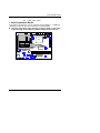
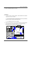
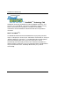
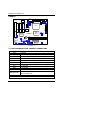
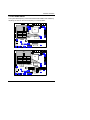
I. Quick Installation Guide :
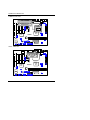
The system bus frequency can be switched between 66MHz ~ 133MHz by
adjusting JP1 & JP33. The CPU Frequency is control by BIOS.
M The CPU speed must match with the frequency RATIO. It will cause
system hanging up if the frequency RATIO is higher than that of CPU.
AC9
7
JP1
1
CPU
CPU
AUTO
66
100
JP1
1-2
2-3
NC
ICH/
82801
YMF
744
6WMM7-1/
6WMM7
GMCH/
82810/
82810-DC100
Back
up
Main
BIOS
Figure 1: other chipset CPU speed setup
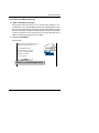
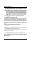
2
6WMM7 Series Motherboard
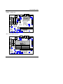
JP1
AC9
7
1
CPU
AUTO
66
100
133
JP1
1-2
2-3
NC
NC
JP33
1-2
YMF
2-3
744
2-3
NC
ICH/
82801
CPU
6WMM7-E
GMCH/
82810E
JP33
1
Back
up
Main
BIOS
Figure 2: for 82810E chipset CPU speed setup
« Note: Please set the CPU host frequency in accordance with your
processor’s specifications. We don’t recommend you to set the
system bus frequency over the CPU’s specification because these
specific bus frequencies are not the standard specifications for
CPU, chipset and most of the peripherals. Whether your system
can run under these specific bus frequencies properly will depend
on your hardware configurations, including CPU, Chipsets,
SDRAM,Cards….etc.
« Note: JP33 is only available when the motherboard use 82810E
chipset.
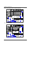
JP17~JP20 (Optional) (See Figure 3) (ICS 9248-73)
CPU
SDRAM
PCI
JP20
JP19
JP18
JP17
AUTO
150
140
133.3
133.3
124
120
114.99
105
100
150
140
133.3
133.3
124
120
114.99
105
33
37.5
35
44.43
33.32
41.33
40
38.33
35
open
1-2
2-3
2-3
1-2
1-2
2-3
2-3
2-3
open
2-3
2-3
1-2
1-2
2-3
2-3
1-2
1-2
2-3
2-3
2-3
1-2
1-2
1-2
1-2
2-3
2-3
2-3
1-2
1-2
2-3
2-3
2-3
2-3
1-2
2-3
3
Quick Installation Guide
100.9
100.23
95
90
83.31
75
70
66.89
100.9
100.23
95
90
124.96
112.5
105
100.33
33.63
33.41
31.67
30
41.65
37.5
35
33.44
1-2
2-3
1-2
2-3
1-2
2-3
1-2
1-2
2-3
2-3
1-2
1-2
2-3
2-3
1-2
1-2
2-3
2-3
1-2
1-2
1-2
1-2
2-3
2-3
2-3
2-3
1-2
1-2
1-2
1-2
1-2
2-3
« Note: We don’t recommend you to set up your system speed to
70,75,83,90,95,105,115,120,124,140 or 150MHz because these
frequencies are not the standard specifications for CPU, Chipset
and most of the peripherals. Whether your system can run under
70,75,83,90,95,105,115,120,124,140 or 150MHz properly will
depend on your hardware configurations: CPU, SDRAM, Cards,
etc.
4
6WMM7 Series Motherboard
JP17/ JP18 / JP19 / JP20 (Optional) :
AC97
1
JP20 1
1
1
JP19YMF
744
1
JP18 1
ICH/
82801
1
100 MHz
JP17
CPU
JP20
JP19
JP18
GMCH/
82810
6WMM7
1
JP17
66 MHz
Backup
BIOS
Main
BIOS
Figure 3
5
Quick Installation Guide
II. Jumper setting :
GN : Green Function Switch
AC97
CPU
YMF
744
ICH/
82801
Backup
BIOS
GMCH/
PIN No. Function
82810
6WMM7
Open Normal Operation
Close Entering Green
Mode
Main
BIOS
GD : Green Function LED
AC97
CPU
YMF
744
−
PIN No.6WMM7
Function
1
LED +
2
LED −
ICH/
82801
1 +
Backup
BIOS
Main
BIOS
6
GMCH/
82810
6WMM7 Series Motherboard
HD : IDE Hard Disk Active LED
AC97
CPU
YMF
744
ICH/
82801
1 +
Backup
BIOS
GMCH/
82810
6WMM7
−
PIN No. Function
1
LED +
2
LED −
Main
BIOS
SPK : External Speaker Connector
AC97
CPU
YMF
744
PIN No.
1
External
ICH/ Speaker
6WMM7 2
82801
3
+ 1
4
Backup
BIOS
Main
BIOS
7
Function
VCC
NC
NC
Data
GMCH/
82810
Quick Installation Guide
J16 : Buzzer Enable (Optional)
AC97
CPU
YMF
744
PIN No. Function GMCH/
82810
Open 6WMM7
Internal Buzzer Disable
Close Internal Buzzer Enable
ICH/
82801
Backup
BIOS
Main
BIOS
RES : Reset Switch
AC97
CPU
YMF
ICH/
82801
744
PIN
No. Function
Open Normal
GMCH/
Operation
82810
6WMM7
Close Reset Hardware
System
Backup
BIOS
Main
BIOS
8
6WMM7 Series Motherboard
PWR : Power LED Connector (as 3 steps ACPI LED)
AC97
CPU
YMF
744
+
1
−ICH/ −
82801
Backup
BIOS
PIN No.
6WMM7
1
2
3
GMCH/
Function
82810
LED +
LED −
LED −
Main
BIOS
PW : Soft Power Connector
AC97
CPU
YMF
744
GMCH/
PIN No. Function
82810
6WMM7
Open Normal operation
Close Soft ON/OFF
ICH/
82801
Backup
BIOS
Main
BIOS
9
Quick Installation Guide
IR / CIR : Infrared Connector
AC97
PIN No. Function
6
1
VCC
2
NC
1
3
IRRX
4
GNDYMF
744
5
IRTX
6
NC
7
CIRRX
8ICH/
VCC 6WMM7
82801
9
NC
10
NC
7
8 CPU9 10
2
3 4
5
GMCH/
82810
Backup
BIOS
Main
BIOS
PS/2 Mouse / Keyboard Connector
AC97
PS/2 Mouse
6
4
ICH/
2
82801
PS/2 Mouse/ Keyboard
Pin No.CPU Function
1
Data
YMF 5
2
NC
744
3
GND
3
4
VCC(+5V)
GMCH/
5
82810Clock
6WMM7
1
6
NC
PS/2 Keyboard
Backup
BIOS
Main
BIOS
10
6WMM7 Series Motherboard
USB : USB Port
AC97
7 8
5 6
YMF
744
1 2 3 4
PIN No.
1
2
3
4
5
6
7
8
Function
USB V0
USB D0USB D0+
GNDCPU
USB V1
USB D1USB D1+
GND
GMCH/
ICH/
82801
6WMM7-1
82810
Backup
BIOS
Main
BIOS
CPU FAN : CPU Fan Connector
AC97
PIN No.
1
2
3
1
ICH/
82801
Function
CPU
GND
+12V
SENSE
6WMM7-1
Main
BIOS
11
GMCH/
82810
Quick Installation Guide
POWER FAN : Power Fan Connector
AC97
CPU
YMF
744
GMCH/
ICH/
82801
1
PIN No.
6WMM7
1
2
3
Backup
BIOS
82810
Function
GND
+12V
SENSE
Main
BIOS
SYSTEM FAN : System Fan Connector
CPU
YMF
744
1
ICH/
82801
PIN No.
1
6WMM7
2
3
Function
GMCH/
GND 82810
+12V
SENSE
Main
BIOS
12
6WMM7 Series Motherboard
IDE1 : Primary IDE Port
AC97
CPU
YMF
744
ICH/
82801
6WMM7-1
GMCH/
82810
Backup
BIOS
1
Main
BIOS
IDE2 : Secondary IDE Port
AC97
CPU
YMF
744
ICH/
82801
6WMM7 -1
Backup
BIOS
GMCH/
82810
1
Main
BIOS
13
Quick Installation Guide
FLOPPY : Floppy Port
AC97
CPU
YMF
744
ICH/
82801
6WMM7 -1
GMCH/
82810
Backup
BIOS
Main
BIOS
1
ATX POWER : ATX Power Connector
1
AC97
11
ICH/
82801
Backup
BIOS
Pin No. Function
3,5,7,13, GND
CPU
15-17
1,2,11
3.3V
YMF
744
4,6,19,20
VCC
10
+12V
GMCH/
12
-12V
82810
18 6WMM7
-5V
8
Power Good
9
5V SB stand by+5V
14
PS-ON(Soft On/Off)
Main
BIOS
14
6WMM7 Series Motherboard
COM B / LPT Port
AC97 PORT
LPT
CPU
COM B
YMF
744
1
ICH/
82801
6WMM7-1
GMCH/
82810
Backup
BIOS
Main
BIOS
VGA : VGA Port
AC97
CPU
YMF
744
ICH/
82801
6WMM7-1
Backup
BIOS
Main
BIOS
15
GMCH/
82810
Quick Installation Guide
COM A : COM A Port
AC97
CPU
COM
A
YMF
744
ICH/
82801
6WMM7-1
GMCH/
82810
Backup
BIOS
Main
BIOS
JP3 : Clear CMOS Function
AC97
CPU
3 2 1
YMF
744
ICH/
82801
PIN No.
Function
GMCH/
82810
1-2 close
Clear
CMOS
6WMM7
2-3 close Normal (Default)
Backup
BIOS
Main
BIOS
16
6WMM7 Series Motherboard
JP13 : PS/2 Keyboard Power On Selection (Optional)
AC97
3
2
1
PIN No. Function
1-2
Keyboard Power on
close Enabled CPU
2-3
Keyboard Power on
YMF
close 744 Disabled (Default)
GMCH/
ICH/
82801
6WMM7-1
82810
Backup
BIOS
Main
BIOS
J8 : Game & Audio Port
AC97
CPU
YMF
744
GAME
MIC GMCH/
82810
6WMM7Line In
Line Out
ICH/
82801
Backup
BIOS
Main
BIOS
17
Quick Installation Guide
J9 : CD Audio Line In
AC97
CPU
1 L G G R
YMF
J9
744
ICH/
GMCH/
82810
6WMM7-1
82801
Backup
BIOS
Main
BIOS
JP25 : AUX_IN
AC97
CPU
JP25
YMF
744
1
PIN No.
ICH/
82801
Backup
BIOS
6WMM7
1
2,3
4
Main
BIOS
18
GMCH/
Function
82810
AUX_L
GND
AUX_R
6WMM7 Series Motherboard
JP16 : TEL(The connector is for Modem with internal voice connector.)
AC97
CPU
1
YMF
744
TEL
ICH/
82801
Backup
BIOS
GMCH/
82810
PIN
No. Function
6WMM7
1
Phone-in
2,3
GND
4
Mono-out
Main
BIOS
J3 : Wake on LAN
AC97
CPU
YMF
744
PIN No.GMCH/Function
1 82810+5VSB
6WMM7
2
2
GND
3
3
Signal
1
ICH/
82801
Backup
BIOS
Main
BIOS
19
Quick Installation Guide
J6 : RING PWR ON (Internal Modem Card Ring PWR On)
AC97
CPU
YMF
744
ICH/
82801
6WMM7
1
PIN No. Function
1 GMCH/
Signal
82810
2
GND
Backup
BIOS
Main
BIOS
JP11 : STR Enable
(If you want to use STR Function, please set jumper JP11 Closed.)
AC97
CPU
YMF
744
1
ICH/
82801
Backup
BIOS
6WMM7
PIN No.
Close
Open
GMCH/
82810
Function
STR Enable
STR Disable
Main
BIOS
20
6WMM7 Series Motherboard
21
Quick Installation Guide
JP9 : STR LED CONN.
AC97
CPU
YMF
744
STR LED Connector
External. ICH/
82801
JP9
Backup
BIOS
1
6WMM7 -1
+
GMCH/
82810
STR LED
Main
BIOS
JP12 : Case Open
AC97
CPU
YMF
744
JP12
ICH/
82801
Backup
BIOS
6WMM7
1
GMCH/
82810
PIN No. Function
1
Signal
2
GND
Main
BIOS
22
6WMM7 Series Motherboard
JP2 : Top Block Lock
AC97
CPU
YMF
744
ICH/
82801
Backup
BIOS
Main
BIOS
GMCH/
82810
6WMM7
PIN No.
Function
Open Top Block Lock
Close Top Block Unlock
(Default).
JP26 : System Boot Option
AC97
CPU
YMF
744
GMCH/
1
ICH/
82801
Backup
BIOS
82810
PIN6WMM7
No.
Function
1-2close
Normal
2-3close
Safe mode
1-2-3open Recovery
Main
BIOS
23
Quick Installation Guide
24
6WMM7 Series Motherboard
TV/DFP :TV-Out / Digital Flat Panel Daughter card connector.
AC97
CPU
1
YMF
744
ICH/
82801
GMCH/
82810
6WMM7-1
Backup
BIOS
Main
BIOS
JP32/JP22 : USB Port Selection (Optional )
AC97
JP22
JP32
JP22
ICH/
JP32
82801
JP32
1
2
3
JP22
1
2
CPU
3
PIN No.
Function
YMF
1-2close
Front Panel USB Enable
744
1-2close
GMCH/
2-3close Back Panel
USB Enable
82810
6WMM7
2-3close
Backup
BIOS
Main
BIOS
25
Quick Installation Guide
JP24 : Front Panel USB Port (Optional )
AC97
CPU
YMF
744
2
9
1
ICH/
82801
Backup
BIOS
10
6WMM7
PIN No.
1,4,5,10
GMCH/
2
82810
3,7,9
6
8
Function
NC
+5V
GND
USBP0+
USBP0-
Main
BIOS
JP28 SPDIF: (Optional , the SPDIF output is capable of providing digital
audio to external speakers or compressed AC3 data to an external Dolby
digital decoder.)
26
6WMM7 Series Motherboard
AC97
1
PIN No.
1 YMF
744
2
3
ICH/
82801
CPU
Function
VCC
SPDIF OUT
GND GMCH/
82810
6WMM7
Backup
BIOS
Main
BIOS
27
Quick Installation Guide
JP4 : Timeout Reboot Function
AC97
CPU
PIN No. Function
OpenYMF Timeout reboot
Close744 No Reboot on timeout
ICH/
82801
6WMM7
JP4
GMCH/
82810
1
Backup
BIOS
Main
BIOS
JP30 : USB Device Wake-up Function (Optional)
AC97
CPU
PIN No. Function
1-2 close Disable USB Device
YMF
744
Wake-up
2-3 close Enable USB Device
wake-up GMCH/
ICH/
82801
82810
6WMM7
1 JP30
Backup
BIOS
Main
BIOS
28
6WMM7 Series Motherboard
YMF 744 : YAHAHA YMF744 (Optional).
AC97
CPU
YMF
744
YAMAHA Sound Chip
ICH/
82801
6WMM7-1
GMCH/
82810
Backup
BIOS
Main
BIOS
JP27 : Onboard H/W Audio Function(Optional).
AC97
CPU
YMF
744
GMCH/
1
Backup
BIOS
PIN
ICH/No.
82801
1-2close
2-3close
82810
Function
Disable H/W Audio
Enabled H/W Audio
(Default)
6WMM7
Main
BIOS
29
Quick Installation Guide
JP31 : AMR (Optional)
AC97
CPU
JP31 PIN No.
1
1-2 close
2-3 close
ICH/
82801
Onboard
CDOEC
Primary
Disabled
YMF
744
AMR Card
Secondary
GMCH/
Primary
82810
6WMM7
Note:
6WMM7/6WMM7-E:
Backup
If M/B has hardware audio (YAMAHA YMF744), your
BIOS
modem riser has been set to “Primary” automatically.
No Jumper JP31 for 6WMM7
Main
BIOS
6WMM7-1:
JP31: 1-2 close: If you use software audio(onboard
CODEC only), your modem riser must be “Secondary”.
JP31: 2-3 close: If you don’t use onboard software
audio, your audio/modem riser must be “Primary”.
Mainboard’s software audio will be disabled.
JP29 : FPSW
AC97
CPU
YMF
744
ICH/
82801
6WMM7-1
Backup
BIOS
Main
BIOS
30
GMCH/
82810
6WMM7 Series Motherboard
BAT1 : For Battery
AC97
Danger of explosion if battery is
incorrectly replaced.
Replace only with the same or
CPU
equivalent type recommended
by the
YMF
744
manufacturer.
Dispose of used batteries according
to the manufacturer’s instructions .
+
ICH/
82801
6WMM7
Backup
BIOS
Main
BIOS
31
GMCH/
82810
Quick Installation Guide
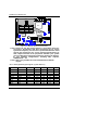
III. Top Performance Test Setting:
The following performance data list is the testing results of some popular
benchmark testing programs.
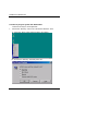
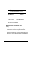
CMOS Setup Utility-Copyright( C ) 1984-1999 Award Software
Advanced Chipset Features
Top Performance
Enabled
Item Help
SDRAM CAS Latency Time
2
SDRAM Cycle Time Tras/Trc
5/7
Menu Level 4
SDRAM RAS-to-CAS Delay
2
SDRAM RAS Precharge Time
2
SDRAM Buffer Strength
AUTO
Delayed Transaction
Disabled
Local Memory Frequency
100MHz
* Onboard Display Cache Setting *
Initial Display Cache
Display cache Timing
Enabled
Auto
↑↓→ ←Move Enter:Select +/-/PU/PD:Value F10:Save ESC:Exit F1:General Help
F5:Previous Values F6:Fail-Safe Defaults F7:Optimized Defaults
Users have to modify the value for each item in chipset features as follow
for top performance setting.
*The above settings have to modify according to different kinds of CPU,
SDRAM, and peripherals for your system to work properly.
* Note: The “Local Memory Frequency 133MHz” function is only
available when motherboard use GMCH 82810E chipset.
32
6WMM7 Series Motherboard
These data are just referred by users, and there is no responsibility for different
testing data values gotten by users. (The different Hardware & Software
configuration will result in different benchmark testing results.)
• CPU
Intel CeleronTM 533MHz Socket 370 processor
• DRAM
(128x1)MB SDRAM (Winbond 902WB W986408BH-8H)
• CACHE SIZE
128 KB included in CPU
• DISPLAY
• STORAGE
Onboard Intel Corporation 810 Graphics Controller
Hub) (4MB SDRAM)
Onboard IDE (IBM DTTA-371800)
• O.S.
Windows NT™ 4.0 SPK5
• DRIVER
Display Driver at 1024 x 768 x 16bit colors x 75Hz.
Intel CeleronTM (Socket
370)
Processor
533MHz (66x8)
Winbench99
CPU mark99
39.4
FPU Winmark 99
2860
Business Disk Winmark 99
3450
Hi-End Disk Winmark 99
5470
Business Graphics Winmark 99
142
Hi-End Graphics Winmark 99
367
Winstone99
Business Winstone99
28.2
Hi-End Winstone99
22.5
33
Quick Installation Guide
34
Suspend to RAM Installation
IV. Suspend to RAM Installation
A.1 Introduce STR function:
Suspend-to-RAM (STR) is a Windows 98 ACPI sleep mode function. When
recovering from STR (S3) sleep mode, the system is able, in just a few
seconds, to retrieve the last “state” of the system before it went to sleep and
recover to that state. The “state” is stored in memory (RAM) before the
system goes to sleep. During STR sleep mode, your system uses only
enough energy to maintain critical information and system functions,
primarily the system state and the ability to recognize various “wake up”
triggers or signals, respectively.
A.2 STR functi on Installation
Please use the following steps to complete the STR function installation.
Step-By-Step Setup
Step 1:
To utilize the STR function, the system must be in Windows 98 ACPI mode.
Putting Windows 98 into ACPI mode is fairly easy.
Setup with Windows 98 CD:
A.
Insert the Windows 98 CD into your CD-ROM drive, select Start, and then
Run.
B.
Type (without quotes) “D:\setup /p j” in the window provided. Hit the
enter key or click OK.『In Windows 98 second edition version, all the bios
version dated 12/01/99 or later are ACPI compatible. Just type" D:\Setup",
the operating system will be installed as ACPI mode.』
C.
After setup completes, remove the CD, and reboot your system
(This manual assumes that your CD-ROM device drive letter is D:).
30
6WMM7 Series Motherboard
31
Suspend to RAM Installation
Step 2:
(If you want to use STR Function, please set jumper JP11 Closed.)
AC97
CPU
YMF
744
1
ICH/
82801
Backup
BIOS
6WMM7
PIN
No.
Close
Open
GMCH/
82810
Function
STR Enable
STR Disable
Main
BIOS
Step 3:
Power on the computer and as soon as memory counting starts, press <Del>.
You will enter BIOS Setup. Select the item “POWER MANAGEMENT SETUP”,
then select “ACPI Suspend Type: S3 (Suspend to RAM)”. Remember to
save the settings by pressing "ESC" and choose the “SAVE & EXIT SETUP”
option.
Congratulation! You have completed the installation and now can use the STR
function.
32
6WMM7 Series Motherboard
A.3 How to put your system into STR mode?
There are two ways to accomplish this:
1. Choose the “Stand by” item in the “Shut Down Windows” area.
A. Press the “Start” button and then select “Shut Down”
B. Choose the “Stand by” item and press “OK”
33
Suspend to RAM Installation
2.
Define the system ”power on” button to initiate STR sleep mode:
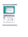
A. Double click “My Computer” and then “Control Panel”
B. Double click the “ Power Management” item.
34
6WMM7 Series Motherboard
C. Select the “Advanced” tab and “Standby” mode in Power Buttons.
Step 4:
Restart your computer to complete setup.
Now when you want to enter STR sleep mode, just momentarily press the
“Power on” button..
A.4 How to recover from the STR sleep mode?
There are seven ways to “wake up” the system:
1. Press the “Power On” button.
2. Use the “PS/2 Keyboard Power On” function.
3. Use the “PS/2 Mouse Power On” function.
4. Use the “Resume by Alarm” function.
5. Use the “Modem Ring On” function.
6. Use the “Wake On LAN” function.
35
Suspend to RAM Installation
7. Use the “USB Device Wake up” function.
A.5 Notices :
1.
In order for STR to function properly, several hardware and software
requirements must be satisfied:
A. Your ATX power supply must comply with the ATX 2.01 specification
(provide more than 720 mA 5V Stand-By current).
B. Your SDRAM must be PC-100 compliant.
2. Jumper JP9 is provided to connect to the STR LED in your system chassis.
[Your chassis may not provide this feature.] The STR LED will be
illuminated when your system is in STR sleep mode.
AC97
CPU
YMF
744
STR LED Connector
External. ICH/
82801
JP9
Backup
BIOS
1
+
6WMM7-1
STR LED
Main
BIOS
36
GMCH/
82810
6WMM7 Series Motherboard
37
Introduce Dual BIOS
V. Introduce Dual BIOS (Optional)
A. What is Dual BIOS Technology?
Dual BIOS means that there are two system BIOS (ROM) on the
motherboard, one is the Main BIOS and the other is Backup BIOS. Under
the normal circumstances, thesystem works on the Main BIOS. If the Main
BIOS is corrupted or damaged, the Backup BIOS can take over while the
system is powered on. This means that your PC will still be able to run
stably as if nothing has happened in your BIOS.
B. How to use Dual BIOS?
a. Boot Screen
Award Modular BIOS v6.00PG, An Energy Star Ally
Copyright (C) 1984-98, Award Software, Inc.
Intel XXXX AGPSet BIOS for XXXX
Check System Health ok , Vcore A =2.00V
Main Processor : CELERON(TM) 533MHz
<CPU ID:0665 , Patch ID:0003>
Memory Test :16384K OK
Award Plug and Play BIOS Extension Vx.x
Copyright (C ) 1998, Award software, Inc.
Press
enter
Dual
<Press
F1 toF1
enterto
Dual
BIOS Utility>
BIOS Utility
36
6WMM7 Series Motherboard
b. Dual BIOS Utility
Dual BIOS Utility V6.60.g.01K
(C) 1999, Gigabyte Technology Co., LTD.
Wide Range Protection
Halt On BIOS Defects
Auto Reco very
Boot From
BIOS Recovery
:Disabled
:Disabled
:Enabled
:Main BIOS
:Main to Backup
F3: Load Default
F7: Save And Restart
F5:Start BIOS Recovery
F9:Exit Without Saving
Use <Space> key to toggle setup
c. Dual BIOS Item explanation:
Wide Range Protection: Disabled(Default), Enabled
Status 1:
If any failure (ex. Update ESCD failure, checksum error or reset…)
occurs in the Main BIOS , just before the Operating System is loaded
and after the power is on, and that the Wide Range Protection is set to
“Enable”, the PC will boot from Backup BIOS automatically.
Status 2:
If the ROM BIOS on peripherals cards(ex. SCSI Cards, LAN Cards,..)
emits signals to request restart of the system after the user make any
alteration on it, the boot up BIOS will not be changed to the Backup
BIOS.
37
Introduce Dual BIOS
Halt On BIOS Defects : Disabled(Default), Enabled
If the BIOS occurs a checksum error or the Main BIOS occurs a WIDE
RANGE PROTECTION error and Halt On BIOS Defects set to Enable, the
PC will show messages on the boot screen, and the system will pause
and wait for the user’s instruction.
If Auto Recovery :Disabled, it will show <or the other key to continue.>
If Auto Recovery : Enabled, it will show <or the other key to Auto
Recover.>
Auto Recovery : Enabled(Default), Disabled
When one of the Main BIOS or Backup BIOS occurs checksum failure, the
working BIOS will automatically recover the BIOS of checksum failure.
(In the Power Management Setup of the BIOS Setting, if ACPI Suspend
Type is set to Suspend to RAM, the Auto Recovery will be set to Enable
automatically.)
(If you want to enter the BIOS setting, please press “Del” key when the
boot screen appears.)
Boot From : Main BIOS(Default), Backup BIOS
Status 1:
The user can set to boot from main BIOS or Backup BIOS.
Status 2:
If one of the main BIOS or the Backup BIOS fails, this item “Boot From :
Main BIOS(Default)” will become gray and will not be changed by user.
BIOS Recovery : Main to Backup
Auto recovery message:
BIOS Recovery: Main to Backup
The means that the Main BIOS works normally and could automatically
recover the Backup BIOS.
BIOS Recovery: Backup to Main
The means that the Backup BIOS works normally and could
automatically recover the Main BIOS.
(This auto recovery utility is set by system automatically and can’t be
38
6WMM7 Series Motherboard
changed by user.)
DualBIOSTM Technology FAQ
GIGABYTE Technology is pleased to introduce DualBIOS technology, a hot
spare for your system BIOS. This newest “Value-added” feature, in a long
series of innovations from GIGABYTE, is available on GA-6WMM7
motherboard. Future GIGABYTE motherboards will also incorporate this
innovation.
TM
What’s DualBIOS
?
On GIGABYTE motherboards with DualBIOS there are physically two BIOS
chips. For simplicity we’ll call one your “Main BIOS” and the other we’ll call your
“Backup” BIOS (your “hot spare”). If your Main BIOS fails, the Backup BIOS
almost automatically takes over on your next s ystem boot. Almost
automatically and with virtually zero down time! Whether the problem is a
failure in flashing your BIOS or a virus or a catastrophic failure of the Main BIOS
chip, the result is the same - the Backup BIOS backs you up, almost
automatically.
39
Introduce Dual BIOS
TM
I. Q: What is DualBIOS
Answer:
technology?
DualBIOS technology is a patented technology from Giga-Byte Technology.
The concept of this technology is based on the redundancy and fault tolerance
TM
theory. DualBIOS technology simply means there are two system BIOSes
(ROM) integrated onto the motherboard. One is a main BIOS, and the other is
a backup BIOS. The mainboard will operate normally with the main BIOS,
however, if the main BIOS is corrupt or damaged for various reasons, the
backup BIOS will be automatically used when the system powered-On. Your
PC will operate as before the main BIOS was damaged, and is completely
transparent to the user.
TM
II. Q: Why does anyone need a motherboard with DualBIOS
technology?
Answer:
In today’s systems there are more and more BIOS failures. The most
common reasons are virus attacks, BIOS upgrade failures, and/or
deterioration of the BIOS (ROM) chip itself.
1. New computer viruses are being found that attack and destroy the system
BIOS. They may corrupt your BIOS code, causing your PC to be unstable or
even not boot normally.
2. BIOS data will be corrupted if a power loss/surge occurs, or if a user
resets the system, or if the power button is pressed during the process of
performing a system BIOS upgrade.
3. If a user mistakenly updates their mainboard with the incorrect BIOS file,
then the system may not be able to boot correctly. This may cause the PC
system hang in operation or during boot.
4. A flash ROM's life cycle is limited according to electronic characteristics.
The modern PC utilizes the Plug and Play BIOS, and is updated regularly.
If a user changes peripherals often, there is a slight chance of damage to
the flash ROM.
With Giga-Byte Technology’s patented DualBIOSTM technology you can
reduce the possibility of hangs during system boot up, and/or loss BIOS data
due to above reasons. This new technology will eliminate valuable system
down time and costly repair bills cause by BIOS failures.
40
6WMM7 Series Motherboard
TM
III. Q: How does DualBIOS
Answer:
technology work?
TM
1. DualBIOS technology provides a wide range of protection during the boot
up procedure. It protects your BIOS during system POST, ESCD update,
and even all the way to PNP detection/assignment.
TM
2. DualBIOS provides automatic recovery for the BIOS. When the first BIOS
used during boot up does not complete or if a BIOS checksum error occurs,
TM
boot-up is still possible. In the DualBIOS utility, the "Auto Recovery" option
will guarantee that if either the main BIOS or backup BIOS is corrupted, the
TM
DualBIOS technology will u se the good BIOS and correct the wrong BIOS
automatically.
TM
TM
3. DualBIOS provides manual recovery for the BIOS. DualBIOS
technology contains a built-in flash utility, which can flash your system BIOS
from backup to main and/or visa versa. There is no need for an
OS-dependent flash utility program.
TM
4. DualBIOS contains a one-way flash utility. The built-in one-way flash utility
will ensure that the corrupt BIOS is not mistaken as the good BIOS during
recovery and that the correct BIOS (main vs. backup) will be flashed. This
will prevent the good BIOS from being flashed.
TM
IV. Q: Who Needs DualBIOS
Answer:
technology?
TM
1. Every user should have DualBIOS technology due to the advancement of
computer viruses.
Everyday, there are new BIOS-type viruses discovered that will destroy your
system BIOS. Most commercial products on the market do not have
TM
solutions to guard against this type of virus intrusion. The DualBIOS
technology will provide a state-of-the-art solution to protect your PC:
Case I.) Vicious computer viruses may wipe out your entire system BIOS.
With a conventional single system BIOS PC, the PC will not be functional
until it is sent for repairs.
TM
Case II.) If the "Auto Recovery" option is enabled in the DualBIOS utility,
and if a virus corrupts your system BIOS, the backup BIOS will automatically
reboot the system and correct the main BIOS.
Case III.) A user may override booting from the main system BIOS. The
TM
DualBIOS utility may be entered to manually change the boot sequence to
boot from the backup BIOS.
41
Introduce Dual BIOS
TM
2. During or after a BIOS upgrade, if DualBIOS detects that the main BIOS is
corrupt, the backup BIOS will take over the boot-up process automatically.
Moreover, it will verify the main and backup BIOS checksums when
TM
booting-up. DualBIOS technology examines the checksum of the main
and backup BIOS while the system is powered on to guarantee your BIOS
operates properly.
3. Power Users will have the advantage of having two BIOS versions on their
mainboard. The benefit is being able to select either version BIOS to suit the
performance system needs.
4. Flexibility for high-end desktop PCs and workstation/servers. In the
TM
DualBIOS utility, the option can be set, "Halt On When BIOS Defects," to be
enabled to halt your system with a warning message thatthe main BIOS has
been corrupted. Most workstation/servers require constant operation to
guarantee services have not been interrupted. In this situation, the "Halt On
When BIOS Defects" message may be disabled to avoid system pauses
during normal booting. Another advantage you gain from Giga-Byte’s
TM
DualBIOS technology is the ability to upgrade from dual 2 Mbit BIOS to
dual 4 Mbit BIOS in the future if extra BIOS storage is need.
42
6WMM7 Series Motherboard
TABLE OF CONTENTS
1.
INTRODUCTION
1.1. PREFACE......................................................................................................... 1-1
1.2. KEY FEATURES............................................................................................... 1-1
1.3. PERFORMANCE LIST.......................................................................................1-3
1.4. BLOCK DIAGRAM............................................................................................ 1-4
®
1.5. INTRODUCE THE INTELCeleronTM / Pentium !!! Socket 370
Processor...............................................................................................................1-5
1.6. INTRODUCE AMR............................................................................................. 1-5
2.
SPECIFICATION
2.1. HARDWARE....................................................................................................2-1
2.2. SOFTWARE.....................................................................................................2-2
2.3. ENVIRONMENT ................................................................................................2-2
3.
HARDWARE INSTALLATION
3.1. UNPACKING.....................................................................................................3-1
3.2. MAIN BOARD LAYOUT................................................................................... 3-2
3.3. QUICK REFERENCE FOR JUMPERS & CONNECTORS......................................3-3
3.4. DRAM INSTALLATION .....................................................................................3-8
3.5. CPU SPEED SETUP..........................................................................................3-9
3.6. CMOS RTC & ISA CFG CMOS SRAM............................................................... 3-10
3.7. SPEAKER CONNECTOR INSTALLATION.........................................................3-10
3.8. HARDWARE RESET SWITCH CONNECTOR INSTALLATION ...........................3-10
3.9. POWER LED CONNECTOR INSTALLATION .....................................................3-11
1
Table of Contents
3.10. IDE & ATAPI DEVICE INSTALLATION............................................................. 3-11
2
Introduction
3.11. PERIPHERAL DEVICE INSTALLATION............................................................ 3-11
3.12. KEYBOARD & PS/2 MOUSE INSTALLATION.................................................3-11
4.
BIOS CONFIGURATION
4.1. ENTERING SETUP............................................................................................ 4-1
4.2. CONTROL KEYS.............................................................................................. 4-1
4.3. GETTING HELP.................................................................................................4-2
4.3.1. Main Menu............................................................................................ 4-2
4.3.2. Status Page Setup Menu / Option Page Setup Menu...........................4-2
4.4. THE MAIN MENU.............................................................................................. 4-2
4.5. STANDARD CMOS FEATURES MENU............................................................. 4-5
4.6. ADVANCED BIOS FEATURES ........................................................................ 4-9
4.7. ADVANCED CHIPSET FEATURES ...................................................................4-12
4.8. INTEGRATED PERIPHERALS............................................................................4-15
4.9. POWER MANAGEMENT SETUP....................................................................... 4-22
4.10. PNP/PCI CONFIGURATIONS ...........................................................................4-27
4.11. PC HEALTH STATUS..................................................................................... 4-29
4.12. FREQUENCY/VOLTAGE CONTROL............................................................... 4-31
4.13. LOAD FAIL-SAFE DEFAULTS....................................................................... 4-33
4.14. LOAD OPTIMIZED DEFAULTS........................................................................ 4-34
4.15. SET SUPERVISOR/USER PASSWORD..........................................................4-35
4.16. SAVE & EXIT SETUP......................................................................................4-36
4.17. EXIT WITHOUT SAVING.................................................................................4-37
APPENDIX ................................................................................................................... A-1
1-3
6WMM7 Series Motherboard
1. INTRODUCTION
1.1. PREFACE
Welcome to use the 6WMM7 motherboard series. It is a CeleronTM /
Pentium ® !!! Socket 370 Processor based PC / AT compatible system with PCI
/ ISA Bus, and has been designed to be the fastest PC / AT system. There are
some new features allow you to operate the system with just the performance
you want.
This manual also explains how to install the motherboard for operation, and
how to set up yo ur CMOS CONFIGURATION with BIOS SETUP program.
Note: The 6WMM7 motherboard series includes 6WMM7(use
82810-DC100 chipset), 6WMM7-1(use 82810 chipset) and
6WMM7-E(use 82810E chipset).
1.2. KEY FEATURES
□
□
□
□
□
□
□
□
□
□
□
□
□
□
□
Intel CeleronTM /Pentium® !!! Socket 370 Processor based PC / AT
compatible main board
Socket 370 Pins ZIF white socket on board.
Built-in AC 97-Link software audio and YAMAHA 744 Hardware audio
(Optional).
Supports CeleronTM /Pentium® !!! Socket 370 processor running at
300-733 MHz. .( The PCB version 2.0 and above have supported Intel
Pentium® !!! 256K Socket 370 Processor.).
INTEL FW82810 chipset, Supports SDRAM / Ultra DMA33/ATA66 IDE /
Keyboard and PS/2 Mouse Power On / ACPI features.
Supports 2xDIMMs using 3.3V SDRAM DIMM module.
Supports 4MB SDRAM Display cache.(Optional)
Supports external Modem Ring-On on COMA & COMB and internal
Modem Ring-On.
Supports PC100 SDRAM 16MB~512MB memory on board.
Supports Wake-up on LAN.
Supports AMR Function.
Supports feature connector for TV-Out or DFP (Digital Flat Panel).
3xPCI Bus slots, 1xISA Bus slots(Optional).
Supports 2 channels Ultra DMA33/ATA66 IDE ports for 4 IDE Devices.
Supports 1x Line in, 1x Line Out, 1x Mic in, 1x CD Line in,1x GAME Port 1
1-1
Introduction
x TEL, 1x SPDIF OUT(Optional).
1-2
6WMM7 Series Motherboard
□
□
□
□
□
Supports 2xCOM (16550), 1xLPT (EPP / ECP/ SPP), 1x1.44MB Floppy
port.
Supports Dual BIOS Function.
Licensed AWARD BIOS, 4M bits FLASH ROM.
24.4 cm x 24.2 cm Micro ATX SIZE form factor, 4 layers PCB.
The PCB version 2.0 and above have supported Intel Pentium ® !!! 256K
Socket 370 Processor
1-3
Introduction
1.3. PERFORMANCE LIST
These data are just referred by users, and there is no responsibility for
different testing data values gotten by users. (The different Hardware &
Software configuration will result in different benchmark testing results.)
• CPU
Intel CeleronTM 533MHz Socket 370 processor
• DRAM
(128x1)MB SDRAM (Winbond 902WB W986408BH-8H)
• CACHE SIZE
128 KB included in CPU
• DISPLAY
• STORAGE
Onboard Intel Corporation 810 Graphics Controller
Hub) (4MB SDRAM)
Onboard IDE (IBM DTTA-371800)
• O.S.
Windows NT™4.0 SPK5
• DRIVER
Display Driver at 1024 x 768 x 16bit colors x 75Hz.
Intel CeleronTM (Socket
370)
Processor
533MHz (66x8)
Winbench99
CPU mark99
39.4
FPU Winmark 99
2860
Business Disk Winmark 99
3450
Hi-End Disk Winmark 99
5470
Business Graphics Winmark 99
142
Hi-End Graphics Winmark 99
367
Winstone99
Business Winstone99
28.2
Hi-End Winstone99
22.5
1-4
6WMM7 Series Motherboard
1-5
Introduction
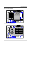
1.4. BLOCK DIAGRAM
66 / 100 /133MHz
14.318MHz
3.3V SDRAM
DIMM Sockets
PGA 370
Host Bus
INTEL
FW82810
(GMCH)
Display cache
Memory 4MB
DRAM Bus
PCI to ISA
Bridge
Winbond
w83628
14.318MHz
ISA Bus
100MHz
PCI Bus
YAMAHA
YMF744
33MHz
INTEL
FW82801
ICH/ICH0
IDE Bus
MIC
48MHz
14.318MHz
33 MHz
USB Ports
USB Bus
AC’97-Link
COM Ports
LPC Bus
I/O
CHIPSET
Winbond
W83627
AC97
L-IN
L-OUT
ICS
9248-73/96
33MHz
Ultra
DMA66/33
IDE Ports
CODEC
LPT Port
Floppy Port
Keyboard
AMR
Slot
PS/2 Mouse
GAME Port
1-6
48 MHz
6WMM7 Series Motherboard
1.5. INTRODUCE THE INTEL Celeron
Processor
TM
/Pentium® !!! Socket 370
Figure 1.1: INTEL CeleronTM /Pentium ® !!! Socket370 Processor
1.6 INTRODUCE AMR
The Audio Modem Riser (AMR) is a new port that supports both audio and
modem. The main purpose of the AMR port is to provide lower cost and higher
levels of integration at all levels of the PC platform.
The backbone of the AMR interface is on AC’97 compliant AC-Link with
support for codes. Motherboard support for an AMR interface are not only
capable of achieving the lowest possible cost for basic PC audio and modem,
but have also introduced increased motherboard flexibility enabling robust,
cost effect ive scalability.
The AMR is done through software and controlled by the motherboard’s I/O
Controller Hub (ICH). There are two types of AMR, one defined as primary and
another defined as secondary. If the motherboard with onboard sound
YAMAHA 744, the AMR must be used primary.
1-7
Specification
2. SPECIFICATION
2.1. HARDWARE
• CPU
− CeleronTM /Pentium ® !!! Socket 370 processor 300–
733 MHz.
− 66/100/133MHz Socket 370 on board.
• PROTECTION
− Speaker Alarm when detect "CPU FAN Failure" or
“CPU Overheat”.
− Automatically slow down CPU speed when "CPU
Overheat".
− H/W monitor power status (±5V, ±12V, VGTL,5VSB,
CPU voltage & CMOS battery voltage).(Optional)
• SPEED
− 66/100/133 MHz system speed.
( 133 MHz system speed is only available when the
motherboard use 82810E chipset).
− 33 MHz PCI-Bus speed.
− 8 MHz AT bus speed.
• DRAM MEMORY
− 2 banks 168 pins DIMM module sockets on board.
− Use 16 / 32 / 64 / 128 / 256MB DIMM module DRAM.
− Supports PC-100 SDRAM 16MB~512MB.
• CACHE MEMORY
− 32 KB 1st cache memory included in CPU.
− 128KB L2 cache memory included in CPU.
− Supports DIB speed mode for L2 Cache.
• I/O BUS SLOTS
− 3 33MHz Master / Slave PCI-BUS.
− 1 8MHz 16 bits ISA BUS (Optional).
• IDE PORTS
− 2 Ultra DMA33/ATA66 Bus Master IDE channels on
board.(Using IRQ14,15)
− Supports Mode 3,4 IDE & ATAPI CD – ROM.
• I/O PORTS
− Supports 2 16550 COM ports.
− Supports 1 EPP/ECP LPT port.
− Supports 1 1.44 /2.88 MB Floppy port.
− Supports 2 USB ports.
− Supports PS/2 Mouse & Keyboard.
2-1
6WMM7 Series Motherboard
• Audio Ports
• GREEN FUNCTION
• BIOS
• DIMENSION
• Display Cache
− 1x Line in
− 1x Line out
− 1x Mic in
− 1x Game Port
− 1x CD Line in
− 1x TEL (Optional)
− 1x SPDIF OUT (Optional)
− Suspend mode support.
− Green switch & ACPI LED support.
− IDE & Display power down support.
− Monitors all IRQ / DMA / Display / I/O events.
− Support Dual BIOS (Optional).
− Supports Plug & Play, DMI Function.
− Micro ATX Form Factor, 4 layers PCB.
− 4MB SDRAM (Optional)
2.2. SOFTWARE
• DRIVER
− IUCD (Bus Master + Sound Driver + LDCM + Utility)
− INTEL 82810 Driver.
• BIOS
− Licensed AWARD BIOS.
− AT CMOS Setup, BIOS / Chipset Setup, Green Setup,
Hard Disk Utility included.
• O.S.
− Operation with MS-DOS , Windows 95,
Windows 98, WINDOWS NT, OS/2, NOVELL and
SCO UNIX.
2.3. ENVIRONMENT
• Ambient Temp.
− 0°C to +50°C (Operating).
• Relative Hum.
− 0 to +85% (Operating).
• Altitude
− 0 to 10,000 feet (Operating).
• Vibration
− 0 to 1,000 Hz.
• Electricity
− 4.75 V to 5.25 V. (Max. 20A current at 5V.)
2-2
Hardware Installation
3.
HARDWARE INSTALLATION
3.1. UNPACKING
The main board package should contain the following:
•
The 6WMM7 Series motherboard.
•
USER'S MANUAL for main board.
•
Cable set for IDE, Floppy devices, [COMB Port Cable (Optional)].
•
CD for main board Utility. [IUCD (Bus Master + Sound Driver + LDCM +
Utility), INTEL 82810 Driver.]
The main board contains sensitive electric components, which can be easily
damaged by static electricity, so the main board should be left in its original
packing until it is installed.
Unpacking and installation should be done on a grounded anti-static mat. The
operator should be wearing an anti static wristband, grounded at the same
point as the anti -static mat.
Inspect the main board carton for obvious damage. Shipping and handling
may cause damage to your board. Be sure there are no shipping and handling
damages on the board before proceeding.
After opening the main board carton, extract the system board and place it only
on a grounded anti-static surface component side up. Again inspect the board
for damage. Press down on all of the socket IC's to make sure that they are
properly seated. Do this only on with the board placed on a firm flat surface.
M DO NOT APPLY POWER TO THE BOARD IF IT HAS BEEN DAMAGED.
3-1
6WMM7 Series Motherboard
3-2
Hardware Installation
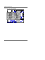
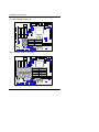
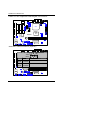
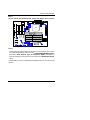
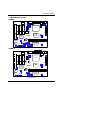
3.2 MAIN BOARD LAYOUT
6WMM7
GAME &
AUDIO
VGA
PCI 3
PCI 2
PCI 1
AMR
JP31
J3
COM A
USB
PS/2
LPT
AC97
ISA 1
JP28
J9
JP25
JP16
COM B
JP30 JP13
CPU FAN
TV/DFP
ATX POWER
CPU
JP27
YMF
744
PWR FAN
J6
JP1
JP26
JP4
ICH/
82801
Main
BIOS
JP2
BANK 1
IDE 2
IR/CIR
JP22
JP24
JP9 SYS FAN
JP20
JP19
JP18
JP17
BANK 0
BAT
JP3
JP12
BZ1 J16 JP32
Backup
BIOS
GMCH/
82810-DC100
6WMM7
IDE 1
J5
JP11
FLOPPY
JP29
×Figure 3.1Ø
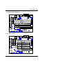
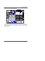
6WMM7-1
GAME &
AUDIO
VGA
AC97
ISA 1
COM A
LPT
USB
PS/2
COM B
PCI 3
PCI 2
PCI 1
J9
JP25
JP16
AMR
J3
JP31
JP13
CPU FAN
ATX POWER
CPU
TV/DFP
YMF
744
PWR FAN
J6
JP1
JP26
JP4
GMCH/
82810
ICH/
82801
6WMM7-1
BAT
Backup
BIOS
JP3
JP12
JP2
BANK 0
BANK 1
IDE 2
IR/CIR
Main
BIOS
IDE 1
J5
JP9 SYS FAN
JP20
JP19
JP18
JP17
FLOPPY
JP29
×Figure3.2Ø
3-3
JP11
6WMM7 Series Motherboard
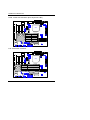
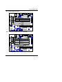
6WMM7-E
GAME &
AUDIO
VGA
PCI 3
PCI 2
PCI 1
AMR
JP31
J3
COM A
USB
PS/2
LPT
AC97
ISA 1
JP28
J9
JP25
JP16
COM B
JP30 JP13
CPU FAN
TV/DFP
YMF
744
ATX POWER
CPU
JP27
PWR FAN
J6
JP26
JP4
ICH/
82801
6WMM7 -E
BAT
JP3
JP12
BZ1 J16 JP32
Backup
BIOS
Main
BIOS
JP2
JP1
JP9 SYS FAN
GMCH/
82810E
JP22
JP24
JP20
JP19
JP18
JP17
BANK 0
BANK 1
IDE 2
IR/CIR
IDE 1
J5
FLOPPY
JP11
JP29
× Figure3.3Ø
3.3. QUICK REFERENCE FOR JUMPERS & CONNECTORS
t I/O Ports Connector
USB
IDE1
IDE2
PS/2
FLOPPY
COMB
COMA
LPT
VGA
ATX Power
GAME & Audio
USB port.
For Primary IDE port.
For Secondary IDE port.
For PS/2 Mouse & Keyboard port.
For Floppy port.
For Serial port2 (COM B){Support Modem Ring On}.
For Serial port1 (COM A){Support Modem Ring On}.
For LPT port.
For VGA Port.
For ATX Power Connector.
For GAME & MIC LINE-IN, LINE-OUT,TEL Port, AUX_IN,
CD_IN, SPDIF OUT.
t Socket 370
3-4
Hardware Installation
For CeleronTM /Pentium ® !!! Socket 370 Processor installed
3-5
6WMM7 Series Motherboard
t IR : INFRARED Connector (IR / CIR) -- Function Option
Pin No.
1
2
3
4
5
6
7
8
9
10
Function
VCC
NC
IRRX
GND
IRTX
NC
CIRRX
VCC
NC
NC
t CPU FAN : CPU FAN Connector
Pin No.
1
2
3
Function
GND.
+12V
SENSE
t PWR FAN: Power FAN Connector
Pin No.
1
2
3
Function
GND.
+12V
SENSE
t SYS FAN: System FAN Connector
Pin No.
1
2
3
Function
GND.
+12V
SENSE
t J16:Buzzer Enable (Optional)
Pin No.
Open
Short
Function
Internal Buzzer Disable
Internal Buzzer Enable
t J6 RING PWR ON :Internal Modem Card Ring PWR On
Pin No.
1
Function
Signal
3-6
Hardware Installation
2
GND
3-7
6WMM7 Series Motherboard
t JP13 : PS/2 Keyboard Power On Selection (Optional)
Pin No.
1-2 short
2-3 short
Function
Enabled PS/2 Keyboard power on.
Disabled PS/2 Keyboard power on(Default).
t J9: CD Audio Line in
Pin No.
1
2
3
4
Function
Left
GND
GND
Right
t JP25:AUX_IN
Pin No.
1
2
3
4
Function
AUX_L
GND
GND
AUX_R
t J3:Wake on LAN
Pin No.
1
2
3
Function
+5V SB
GND
Signal
t TEL : The connector for Modem with internal voice connector.
Pin No.
1
2,3
4
Function
Phone-in
GND
Mono-out
t JP11:STR Enable
Pin No.
Close
Open
Function
STR Enable
STR Disable
t JP12: Case Open
Pin No.
1
Function
Signal
3-8
Hardware Installation
2
GND
3-9
6WMM7 Series Motherboard
t JP26 : System Boot Option
Pin No.
1-2 short
2-3 short
1-2-3open
Function
Normal
Safe Mode
Recovery
t JP2: Top Block Lock
Pin No.
Open
Short
Function
Top Block Lock.
Top Block Unlock (Default).
t JP4: Timeout Reboot
Pin No.
Open
Short
Function
Timeout Reboot.
No Reboot.
t JP27: Onboard H/W Audio (Optional)
Pin No.
1-2 short
2-3 short
Function
Disabled H/W Audio.
Enabled H/W Audio.(Default)
t JP32/ JP22: USB Port Selection (Optional)
Pin No.
1-2 short
2-3 short
Function
Front Panel USB Port Enabled.
Back Front Panel USB Port Enabled.
t JP28: SPDIF (Optional)
Pin No.
1
2
3
Function
VCC
SPDIF OUT
GND
t JP3 : CLEAR CMOS
Pin No.
1-2 short
2-3 short
Function
Clear CMOS
Normal operation (Default).
3-10
Hardware Installation
t JP24: Front Panel USB Port (Optional)
Pin No.
1,4,5,10
2
3,7,9
6
8
Function
NC
+5V
GND
USB P0+
USB P0-
t JP30: USB Device wake-up (Optional)
Pin No.
1-2
2-3
Function
Disable USB Device wake-up.
Enable USB Device wake-up.
J5 : For 2X11 PINs Jumper
PWR P+P−P HD GN
1 −
1
GD
J5
1
1
RES
SPK
Soft PWR: Soft Power Connector
Open: Normal Operation
Short: Power On/Off
RES: Reset Switch
Open: Normal Operation
Short: For Hardware Reset System
−
−
P+P P : Power LED
1
PIN 1 : LED anode (+)
PIN 2 : LED cathode (−)
PIN 3 : LED cathode (−)
3-11
6WMM7 Series Motherboard
SPK: Speaker Connector
+
−
1
PIN 1 : VCC (+)
PIN 2 : NC
PIN 3 : NC
PIN 4 : Data (−)
HD: IDE Hard Disk Active LED
1
PIN 1: LED anode (+)
PIN 2: LED cathode (−)
GN: Green Function Switch
Open : Normal operation
Short : Entering Green Mode
GD: Green LED
1
PIN 1 : LED anode (+)
PIN 2 : LED cathode (− )
3.4. DRAM INSTALLATION
The main board can be installed with 16 / 32 / 64 / 128 / 256 MB 168 pins DIMM
module DRAM, and the DRAM speed must 100 MHz for SDRAM when system
bus speed is set to 66MHz ,100MHz, the DRAM memory system on main
board consists of bank 0 and bank 1.
Since 168 pins DIMM module is 64 bits width, therefore 1 piece of DIMM
module may match a 64 bits system. The total memory size is 16 MB ~ 512MB
SDRAM . The DRAM installation position refer to Figure 3.1, and notice the Pin
1 of DIMM module must match with the Pin 1 of DIMM socket. Insert the DIMM
module into the DIMM socket at Vertical angle. If there is a wrong direction of
Pin 1, the SDRAM DIMM module could not be inserted into socket completely.
3-12
Hardware Installation
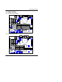
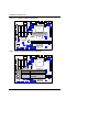
3.5. CPU SPEED SETUP
The system bus frequency can be switched between 66MHz and 133MHz by
adjusting JP1 & JP33. The CPU Frequency is control by BIOS.
AC9
7
JP1
1
CPU
CPU
AUTO
66
100
JP1
1-2
2-3
NC
YMF
744
6WMM7-1/
6WMM7
ICH/
82801
GMCH/
82810/
82810-DC100
Back
up
Main
BIOS
Figure 1: other chipset CPU speed setup
JP1
AC9
7
1
CPU
AUTO
66
100
133
JP1
1-2
2-3
NC
NC
ICH/
82801
JP33
1-2
YMF
2-3
744
2-3
NC
CPU
6WMM7-E
GMCH/
82810E
JP33
1
Back
up
Main
BIOS
Figure 2: for 82810E chipset CPU speed setup
3-13
6WMM7 Series Motherboard
M The CPU speed must match with the frequency RATIO. It will cause
system hanging up if the frequency RATIO is higher than that of CPU.
« Note: Please set the CPU host frequency in accordance with your
processor’s specifications. We don’t recommend you to set the
system bus frequency over the CPU’s specification because these
specific bus frequencies are not the standard specifications for
CPU, chipset and most of the peripherals. Whether your system
can run under these specific bus frequencies properly will depend
on your hardware configurations, including CPU, Chipsets, SDRAM,
Cards ….etc.
« Note: JP33 is only available when the motherboard use 82810E
chipset.
3.6. CMOS RTC & ISA CFG CMOS RAM
There're RTC & CMOS RAM on board; they have a power supply from external
battery to keep the DATA inviolate & effective. The RTC is a REAL-TIME CLOCK
device, which provides the DATE & TIME to system. The CMOS RAM is used for
keeping the information of system configuration, so the system can
automatically boot OS every time. Since the lifetime of internal battery is 5
years, the user can change a new Battery to replace old one after it cannot
work.
M Danger of explosion if battery is incorrectly replaced.
M Replace only with the same or equivalent type recommended by the
manufacturer.
M Dispose of used batteries according to the manufacturer’s instructions.
3.7. SPEAKER CONNECTOR INSTALLATION
There is a speaker in AT system for sound purpose. The 4 - Pins connector
SPK is used to connect speaker.
3.8. HARDWARE RESET SWITCH CONNECTOR INSTALLATION
The RESET switch on panel provides users with HARDWARE RESET function.
The system will do a cold start after the RESET switch is pushed and released
by user. The RESET switch is a 2 PIN connector and should be installed to
RES on main board.
3-14
Hardware Installation
3.9. POWER LED CONNECTOR INSTALLATION
System has power LED lamp on the panel of chassis. The power LED will light
on off or flash to indicate which step on the system. The connector should be
connected to P+P-P- of main board in a correct direction.
3.10. IDE & ATAPI DEVICE INSTALLATION
There are two-Enhanced PCI IDE ports ( IDE1, IDE2 ) on board, which following
ATAPI standard SPEC. Each IDE port can connected to two ATAPI devices (IDE
Hard Disk, CD-ROM or Tape Driver), so total four ATAPI devices can exist in a
system. The HD is the active LED port for ATAPI devices.
3.11. PERIPHERAL DEVICE INSTALLATION
After the I/O device installation and jumpers setup, the main board can be
mounted into the chassis and fixed by screw. To complete the main board
installation, the peripheral device could be installed now. The basic system
needs a display interface card. If the PCI - Bus device is to be installed in the
system, any one of three PCI - Bus slots can be used.
3.12. KEYBOARD & PS/2 MOUSE INSTALLATION
The main board supports PS/2 Mouse. The BIOS will auto detect whether the
PS/2 Mouse is installed or not & assign IRQ12 for PS/2 Mouse port if it is
installed. After installing the peripheral device, the user s hould check
everything again, and ready power-on the system.
3-15