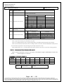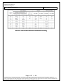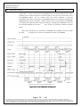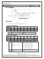
1
i87 User Manual
V1.2
Page:
: 1
/ 82
The information contained herein shall not be changed without prior written permission of iMQ. iMQ reserves the right to change the
information in this document without prior notice. Please contact iMQ to obtain the latest version of product specification before placing
your order. Use of iMQ devices in life support and/or safety applications is entirely at the buyer's risk, and the buyer agrees to defend,
indemnify and hold harmless iMQ from any and all damages, claims, suits or expenses resulting from such use.
漢芝電子股份有限公司
iMQ Technology Inc.
Title: iMQ i87 User Manual
Version:V1.2
Contents
1.
2.
3.
Change History………………………………………………………………………………
History……………………………………………………………………………………………………………………
……………………………………………………………………………………………………………………………………
……………………………………………………5
………………5
Overview of
of iMQ i87 User Manual ................................................................
................................................................................................
..........................................................................
.......................................... 6
................................................................
................................................................
..................................................
Central Processing Unit (CPU) ................................
................................
................................
.................. 7
3.1 General Concept ................................................................................................................................. 7
3.2 Stack Area and Stack Pointer ........................................................................................................... 7
3.2.1 Stack Area .................................................................................................................................. 7
3.2.2 Stack Pointer ............................................................................................................................. 7
3.3 Program Counter (PC) ........................................................................................................................ 9
3.3.1 Program Counter - PC ............................................................................................................ 9
3.3.2 Effects of Jump Instructions on the PC Value ................................................................. 9
3.4 General-Purpose Register ................................................................................................................ 10
3.4.1 A Registers ............................................................................................................................... 10
3.4.2
3.4.3
3.4.4
3.4.5
C Registers ............................................................................................................................... 10
DE Registers ............................................................................................................................ 11
HL Registers ............................................................................................................................ 11
16-Bit General-Purpose Registers (IX, IY) ......................................................................... 11
3.5 Program Status Word (PSW) .......................................................................................................... 11
3.5.1 Zero Flag (ZF) ......................................................................................................................... 13
3.5.2 Carry Flag (CF)........................................................................................................................ 13
3.5.3
3.5.4
3.5.5
3.5.6
Half Carry Flag (HF) .............................................................................................................. 13
Sign Flag (SF) .......................................................................................................................... 13
Overflow Flag (VF)................................................................................................................ 13
Jump Status Flag (JF) ........................................................................................................... 14
3.5.7 Register Bank Selector (RBS)............................................................................................... 14
3.6 Low Power Consumption Function for Peripherals ................................................................ 15
3.7 Key-on Wakeup (KWU) .................................................................................................................... 16
3.7.1 Configuration ......................................................................................................................... 16
3.7.2 Control...................................................................................................................................... 17
3.7.3 Function ................................................................................................................................... 18
3.7.3.1 Setting KWUCRn and P4PU Registers ................................................................. 18
3.7.3.2 Starting STOP Mode ................................................................................................. 18
3.7.3.3 Releasing STOP Mode .............................................................................................. 18
4. Reset Function…………………………..…………………………………………………………….
Function…………………………..…………………………………………………………….………………
…………………………..…………………………………………………………….……………….
………………. ……………….
……………….…….
…….20
4.1 Reset Control Circuit ......................................................................................................................... 20
Page:
: 2
/ 82
The information contained herein shall not be changed without prior written permission of iMQ. iMQ reserves the right to change the
information in this document without prior notice. Please contact iMQ to obtain the latest version of product specification before placing your
order. Use of iMQ devices in life support and/or safety applications is entirely at the buyer's risk, and the buyer agrees to defend, indemnify and
hold harmless iMQ from any and all damages, claims, suits or expenses resulting from such use.
漢芝電子股份有限公司
iMQ Technology Inc.
Title: iMQ i87 User Manual
Version:V1.2
4.1.1 Configuration ......................................................................................................................... 20
4.1.2 Control...................................................................................................................................... 20
4.1.3 Function ................................................................................................................................... 22
4.1.4 Reset Signal Generating Factors ....................................................................................... 24
4.1.4.1 External Reset Input (RESETB Pin Input) ............................................................. 24
4.1.4.2 Power-on Reset .......................................................................................................... 25
4.1.4.3 Voltage Detection Reset ......................................................................................... 25
4.1.4.4
4.1.4.5
4.1.4.6
4.1.4.7
Watchdog Timer Reset ............................................................................................ 25
System Clock Reset.................................................................................................... 25
Internal Factor Reset Detection Status Register................................................ 25
How to Use P10 as an External Reset ................................................................. 26
4.2 Power-on Reset Circuit ..................................................................................................................... 26
4.2.1 Configuration ......................................................................................................................... 26
4.2.2 Function ................................................................................................................................... 27
4.3 Voltage Detection Circuit ................................................................................................................ 28
4.3.1 Configuration ......................................................................................................................... 28
4.3.2 Control...................................................................................................................................... 29
4.3.3 Function ................................................................................................................................... 30
4.3.3.1 Reading the 8-bit Up Counter ............................................................................... 30
4.3.3.2 Selecting the Voltage Detection Operation Mode .......................................... 31
4.3.3.3 Selecting the Detection Voltage Level ................................................................ 31
4.3.3.4 Voltage Detection Flag and Voltage Detection Status Flag ......................... 31
4.3.3.5 Selecting the STOP Mode Release Signal ........................................................... 32
4.3.4 Register Setting ...................................................................................................................... 33
5. Timer / Counter
Counter………………………………….……………….………….…....………….…
………………………………….……………….………….…....………….………
……………………
………………..………………
………………..…….
…….35
………………………………….……………….………….…....………….…
……
………………
35
5.1 Watchdog Timer (WDT) .................................................................................................................. 35
5.1.1 Configuration ......................................................................................................................... 35
5.1.2 Control...................................................................................................................................... 35
5.1.3 Function ................................................................................................................................... 37
5.1.3.1 Setting of Enabling / Disabling the Watchdog Timer Operation................ 37
5.1.3.2 Setting the Clear Time of the 8-bit Up Counter ................................................ 38
5.1.3.3 Setting the Overflow Time of the 8-bit Up Counter ........................................ 39
5.1.3.4 Setting an Overflow Detection Signal of the 8-bit Up Counter ................... 39
5.1.3.5 Writing the Watchdog Timer Control Codes .................................................... 40
5.1.3.6 Reading the 8-bit Up Counter ............................................................................... 40
5.1.3.7 Reading the Watchdog Timer Status................................................................... 40
Page:
: 3
/ 82
The information contained herein shall not be changed without prior written permission of iMQ. iMQ reserves the right to change the
information in this document without prior notice. Please contact iMQ to obtain the latest version of product specification before placing your
order. Use of iMQ devices in life support and/or safety applications is entirely at the buyer's risk, and the buyer agrees to defend, indemnify and
hold harmless iMQ from any and all damages, claims, suits or expenses resulting from such use.
漢芝電子股份有限公司
iMQ Technology Inc.
Title: iMQ i87 User Manual
Version:V1.2
5.2 Divider Output (DVOB) ................................................................................................................... 41
5.2.1 Configuration ......................................................................................................................... 41
5.2.2 Control...................................................................................................................................... 42
5.2.3 Function ................................................................................................................................... 42
5.3 Time Base Timer (TBT) ...................................................................................................................... 43
5.3.1 Configuration ......................................................................................................................... 43
5.3.2 Control...................................................................................................................................... 44
5.3.3 Function ................................................................................................................................... 44
5.4 8-bit Timer Counters ......................................................................................................................... 45
5.4.1 Configuration ......................................................................................................................... 46
5.4.2 Control...................................................................................................................................... 47
5.4.2.1 Timer Counter 00 ...................................................................................................... 47
5.4.2.2 Timer Counter 01 ...................................................................................................... 48
5.4.2.3 Common to Timer Counters 00 and 01.............................................................. 49
5.4.2.4 Operation Modes and Usable Source Clocks .................................................... 50
5.4.3 Low Power Consumption Function ................................................................................. 51
5.4.4 Function ................................................................................................................................... 52
5.4.4.1 8-bit Timer Mode ....................................................................................................... 52
5.4.4.2 8-bit Event Counter Mode ...................................................................................... 55
5.4.4.3 8-bit Pulse Width Modulation (PWM) Output Mode ...................................... 56
5.4.4.4 8-bit Programmable Pulse Generate (PPG) Output Mode ............................ 61
5.4.4.5
5.4.4.6
5.4.4.7
5.4.4.8
16-bit Timer Mode..................................................................................................... 65
16-bit Event Counter Mode .................................................................................... 68
12-bit Pulse Width Modulation (PWM) Output Mode .................................... 70
16-bit Programmable Pulse Generate (PPG) Output Mode .......................... 76
5.5 Real Time Clock (RTC) ....................................................................................................................... 79
5.5.1 Configuration ......................................................................................................................... 80
5.5.2 Control...................................................................................................................................... 80
5.5.3 Function ................................................................................................................................... 81
5.5.3.1 Low Power Consumption Function..................................................................... 81
5.5.3.2 Enabling / Disabling the Real Time Clock Operation ..................................... 81
5.5.3.3 Selecting the Interrupt Generation Interval....................................................... 81
5.5.4 Real Time Clock Operation ................................................................................................. 81
5.5.4.1 Enabling the Real Time Clock Operation ........................................................... 81
5.5.4.2. Disabling the Real Time Clock Operation.......................................................... 82
Page:
: 4
/ 82
The information contained herein shall not be changed without prior written permission of iMQ. iMQ reserves the right to change the
information in this document without prior notice. Please contact iMQ to obtain the latest version of product specification before placing your
order. Use of iMQ devices in life support and/or safety applications is entirely at the buyer's risk, and the buyer agrees to defend, indemnify and
hold harmless iMQ from any and all damages, claims, suits or expenses resulting from such use.
漢芝電子股份有限公司
iMQ Technology Inc.
Title: iMQ i87 User Manual
Version:V1.2
1. Change History
Version
V0.9
Approved
Date
Description
2011/09/23 新建立
Issuer
許平育
1. 將 Stack Area/Point, Program Counter 等 CPU 相關資訊列入
V0.91
2011/10/14
3.1 『General Concept』
。
許平育
2. 將 Registers 與 Program Status Word (PSW)章節重新編排。
V0.92
2011/12/06
將 Functional Description 拆成 CPU、Reset Function、與 Timer
/ Counter 等章節,以方便查閱。
許平育
1. 修正 Figure 4.1 中,部分 MQ8S 系列產品可能沒有 External
Reset Input 之描述。
2. 修正「4.1.2 Control」之 SYSCR4 暫存器資訊。
3. 將「5.3.2 Control」中 TBTCR 暫存器之 TBTCK 在 110 且
V1.0
2012/05/18
DV9CK=1 時之頻率,由 fs/24 改為 fs/23。
4. 更 新 5.4.2.3 之 POFFCR0 (Low Power Consumption
許平育
Register 0)暫存器內容。
5. 將 中 斷 名 稱 INTT00 與 INTT01 分 別 改 成 INTTC00 與
INTTC01,並將 5.20、5.23、與 5.24 中「INTTC00 interrupt
request」修正成「INTTC01 interrupt request」。
1. 在「3.4.2 General-Purpose Register」中加註部分 iMQ IC 可
V1.1
2012/11/27
能僅有 1 組 Bank 0 (比如 MQ8602)。
2. 修改「4.3.2 Control」中 VDCR3 暫存器之 LVD 誤差值,以
許平育
符合實際量測結果。
1. 修正「4.3.3 Function」之內容,以符合 iMQ IC 實際規格。
V1.2
2013/02/01 2. 修正「5.2.3 Function」之打字與編排錯誤。
3. 修正 Table 5.6 與 Table 5.7。
Page:
: 5
李海明
許平育
/ 82
The information contained herein shall not be changed without prior written permission of iMQ. iMQ reserves the right to change the
information in this document without prior notice. Please contact iMQ to obtain the latest version of product specification before placing your
order. Use of iMQ devices in life support and/or safety applications is entirely at the buyer's risk, and the buyer agrees to defend, indemnify and
hold harmless iMQ from any and all damages, claims, suits or expenses resulting from such use.
漢芝電子股份有限公司
iMQ Technology Inc.
Title: iMQ i87 User Manual
Version:V1.2
2. Overview of iMQ i87 User Manual
iMQ MQ8S MCU series 8-bit MCU adopts iMQ i87 8-bit MCU core. It’s a powerful MCU core, with 1T
instruction cycle, various timer / counter resources, interrupt resources, I/O options, multiple operation
modes and flexible memory configuration. Integrated with accurate analog features, such as voltage
regulators, internal / external clocking circuits, voltage detectors, power-on reset and analog-to-digital
converters (ADC), MQ8S MCU series provides complete solutions for wide MCU applications.
In this “iMQ i87 User Manual”, general functions of the MCU, such as registers, flag information, timers /
counter information and reset / detection circuit are described in detailed. For specific functions of each
MQ8S MCU product, such as program / data memory, special function register, interrupts, system clocking,
operation modes and I/O port information, please refer to the MQ8S MCU datasheet.
Please note that in this document, 64K Bytes or smaller memory style is used. Therefore, the address format
will be 0x0000 (or 0x0000H) to 0xFFFF (or 0xFFFFH).
Note that pin names with low-active values, such as STOP, PWM0, PWM1, PPG0, PPG1, INT0, INT5, DVO,
and so on, are presented by ending with “B” in the content, meaning “bar” for inversion. Therefore, they
are written as STOPB, PWM0B, PWM1B, PPG0B, PPG1B, INT0B, INT5B, DVOB and so on.
Besides, to indicate certain bit name in a register, the representation REGISTER_NAME <BIT_NAME> is used
in this document. For example, ILL <IL5> indicates the bit IL5 of the ILL (Interrupt Latch) register.
Page:
: 6
/ 82
The information contained herein shall not be changed without prior written permission of iMQ. iMQ reserves the right to change the
information in this document without prior notice. Please contact iMQ to obtain the latest version of product specification before placing your
order. Use of iMQ devices in life support and/or safety applications is entirely at the buyer's risk, and the buyer agrees to defend, indemnify and
hold harmless iMQ from any and all damages, claims, suits or expenses resulting from such use.
漢芝電子股份有限公司
iMQ Technology Inc.
Title: iMQ i87 User Manual
Version:V1.2
3. Central Processing Unit (CPU)
3.1 General Concept
The introduction of the powerful central processing unit (CPU) of iMQ i87 8-bit MCU core can be
divided into eight major parts: (1) Stack Area / Pointer, (2) Program Counter (PC), (3) General Purpose
Registers, (4) Program Status Word (PSW), (5) Low Power Consumption Function, (6) Key-on Wakeup,
(7) Addressing Space of Program / Data Memory and Special Function Registers (SFR), and (8)
Operation Modes. This “iMQ i87 User Manual” illustrates parts (1) to (6) in detail. As to parts (7) and (8),
please refer to MQ8S MCU datasheet specifically.
The system clock is derived from either a crystal or an oscillator. It is internally divided into default four
non-overlapping clocks, which can be no division, too. One instruction cycle consists of four system
clock cycles. Instruction fetching and execution are pipelined in such a way that a fetch takes one
instruction cycle while decoding and execution takes the next instruction cycle. The pipelining scheme
makes it possible for each instruction to be effectively executed in a cycle. If an instruction changes the
value of the program counter, two cycles are required to complete the instruction.
3.2 Stack Area and Stack Pointer
3.2.1 Stack Area
A stack is an area in memory for temporarily saving the PC, PSW and other values during
subroutines and interrupts.
When a subroutine is called by the [CALL mn] or [CALLV n] instruction, the CPU pushes (saves) the
high-order and low-order bytes of the return address on the stack before jumping to the
subroutine entry address. When the software interrupt instruction, SWI, is executed and when a
hardware interrupt is accepted, the CPU saves the PSW and then return address on the stack.
When the return-from-subroutine instruction, RET, is executed, the CPU pops (restores) the return
address into the PC. When the return-from-interrupt instruction, RETI or RETN, is executed, the CPU
restores the PC and PSW from the stack.
A stack can be allocated anywhere in the data area.
3.2.2 Stack Pointer
The Stack Pointer (SP) is a 16-bit register that holds the address of the next available location on
the stack. The SP is post-decremented on subroutine calls, PUSH operations and interrupts, and
pre-incremented on returns from subroutines and interrupts and POP operations. The stack grows
downwards from high addresses to low addresses as it is filled.
Page:
: 7
/ 82
The information contained herein shall not be changed without prior written permission of iMQ. iMQ reserves the right to change the
information in this document without prior notice. Please contact iMQ to obtain the latest version of product specification before placing your
order. Use of iMQ devices in life support and/or safety applications is entirely at the buyer's risk, and the buyer agrees to defend, indemnify and
hold harmless iMQ from any and all damages, claims, suits or expenses resulting from such use.
漢芝電子股份有限公司
iMQ Technology Inc.
Title: iMQ i87 User Manual
Version:V1.2
Figure 3.1 Stack Pointer
Figure 3.2 shows the contents of the stack and the SP register as each of the following instructions
is executed.
The SP register defaults to 0x00FF upon hardware reset.
Like an index register, the SP register can be modified by using load / store and ALU instructions.
The SP register can also be used as an index register in Indexed Addressing.
Figure 3.2 Stack
Page:
: 8
/ 82
The information contained herein shall not be changed without prior written permission of iMQ. iMQ reserves the right to change the
information in this document without prior notice. Please contact iMQ to obtain the latest version of product specification before placing your
order. Use of iMQ devices in life support and/or safety applications is entirely at the buyer's risk, and the buyer agrees to defend, indemnify and
hold harmless iMQ from any and all damages, claims, suits or expenses resulting from such use.
漢芝電子股份有限公司
iMQ Technology Inc.
Title: iMQ i87 User Manual
Version:V1.2
3.3 Program Counter (PC)
3.3.1 Program Counter - PC
The Program Counter (PC) is an 8-bit register that holds the address of next instruction to be
executed in the code area. When the reset signal is released, the CPU loads the reset vector stored
in the vector table (at 0xFFFF and 0xFFFE in MCU mode) into the PC; thus the program can start at
an arbitrary address. The iMQ i87 Series is pipelined; that is, CPU instructions are pre-fetched.
Therefore, the PC points to an address two bytes after the address of the instruction being
executed. For example, the PC contains 0xC125 while the single-byte instruction stored at 0xC123
is being executed.
Figure 3.3 Program Counter
3.3.2 Effects of Jump Instructions on the PC Value
There are relative and absolute jump instructions. The jump destination is limited within the code
area; a jump cannot occur to the data area. The following describes the effects of jump instructions
on the PC value.
(1) Relative Jump Instruction with a 55-bit Displacement (JRS cc, $ + 2 + d)
When the memory location at 0xE8C4 contains the instruction "JRS T, $ + 2 + 0x08", if JF = 1, the
PC is incremented by 0x08; i.e., a jump occurs to the address 0xE8CE. (The PC points to an
address two bytes after the address of the instruction being executed. In this example, the PC
contains 0xE8C4 + 2 = 0xE8C6 before the jump.)
(2) Relative Jump Instructions
Instructions with an 88-bit Displacement (JR cc, $ + 2 + d / JR cc, $ + 3 + d)
When the memory location at 0xE8C4 contains the instruction "JR Z, $ + 2 + 0x80", if ZF = 1, a
jump occurs to an address that is calculated by PC + 0xFF80 (-128). Thus the jump destination is
0xE846.
(3) 1616-bit Absolute Jump Instruction (JP a)
When the memory location at 0xE8C4 contains the instruction "JP 0xC235", a jump occurs
unconditionally to the address 0xC235. The absolute jump instruction can jump to a location
within the full range of the code area (for example, 4K Bytes for MQ8601, MQ8602, and
MQ8801).
Page:
: 9
/ 82
The information contained herein shall not be changed without prior written permission of iMQ. iMQ reserves the right to change the
information in this document without prior notice. Please contact iMQ to obtain the latest version of product specification before placing your
order. Use of iMQ devices in life support and/or safety applications is entirely at the buyer's risk, and the buyer agrees to defend, indemnify and
hold harmless iMQ from any and all damages, claims, suits or expenses resulting from such use.
漢芝電子股份有限公司
iMQ Technology Inc.
Title: iMQ i87 User Manual
Version:V1.2
3.4 GeneralGeneral-Purpose Register
The iMQ i87 Series has two duplicate banks of eight 8-bit registers called W, A, B, C, D, E, H and L. These
registers can be used as 16-bit register pairs called WA, BC, DE and HL.
The general-purpose registers are not mapped to the address space. The contents of the
general-purpose registers are undefined after power-up and reset.
Figure 3.4 GeneralGeneral-Purpose Registers
The W, A, B, C, D, E, H and L registers are individually used by the 8-bit load/store and ALU instructions.
The WA, BC, DE and HL register pairs are used by the 16-bit load/store and ALU instructions. These
registers also provide the functionalities discussed in the following subsections in addition to the
common characteristics as general-purpose registers.
Note that some iMQ MCU, such as MQ8602, has only general-purpose register, bank0.
3.4.1 A Registers
Bit manipulation instructions can use the A register to specify a bit position in a register whose
value should be tested or changed.
The A register is also used as an offset register in PC-Relative Register Indirect Addressing (PC + A).
3.4.2 C Registers
For divide instructions, the C register holds the divisor. The remainder is written back into the
upper byte of the register pair specified as the dividend; the quotient is written back into the lower
byte.
The C register is also used as an offset register in Register Indexed Addressing (HL + C).
Page:
: 10
/
82
The information contained herein shall not be changed without prior written permission of iMQ. iMQ reserves the right to change the
information in this document without prior notice. Please contact iMQ to obtain the latest version of product specification before placing your
order. Use of iMQ devices in life support and/or safety applications is entirely at the buyer's risk, and the buyer agrees to defend, indemnify and
hold harmless iMQ from any and all damages, claims, suits or expenses resulting from such use.
漢芝電子股份有限公司
iMQ Technology Inc.
Title: iMQ i87 User Manual
Version:V1.2
3.4.3 DE Registers
In Register Indirect Addressing, the DE register holds the address of the memory location where
the operand resides.
3.4.4 HL Registers
In Register Indirect Addressing, the HL register holds the address of the memory location where
the operand resides. In Indexed Addressing, the HL register is used as an index register.
3.4.5 1616-Bit GeneralGeneral-Purpose Registers (IX, IY)
The device has two duplicate banks of two 16-bit general-purpose registers called IX and IY. In
Register Indirect Addressing, these registers hold the address of the memory location where the
operand resides. In Indexed Addressing, they are used as index registers.
The contents of the IX and IY registers are undefined after power-up and reset.
Figure 3.5 1616-Bit GeneralGeneral-Purpose Registers
The load/store and ALU instructions can also use the IX and IY registers as 16-bit general-purpose
registers.
3.5 Program Status Word (PSW)
The Program Status Word, which resides at address 0x003F in the SFR, consists of the following seven
flags:
Jump Status Flag (JF)
Zero Flag (ZF)
Carry Flag (CF)
Half Carry Flag (HF)
Sign Flag (SF)
Overflow Flag (VF)
Register Bank Selector (RBS)
Page:
: 11
/
82
The information contained herein shall not be changed without prior written permission of iMQ. iMQ reserves the right to change the
information in this document without prior notice. Please contact iMQ to obtain the latest version of product specification before placing your
order. Use of iMQ devices in life support and/or safety applications is entirely at the buyer's risk, and the buyer agrees to defend, indemnify and
hold harmless iMQ from any and all damages, claims, suits or expenses resulting from such use.
漢芝電子股份有限公司
iMQ Technology Inc.
Title: iMQ i87 User Manual
Version:V1.2
Dedicated instructions are available to access the PSW. General load instructions can also be used to
read the PSW.
Organization
Organization of the PSW
PSW
(0x003FH)
7
6
5
4
3
2
1
0
JF
ZF
CF
HF
SF
VF
RBS
-
The PSW consists of seven bits of status information that are set or cleared by CPU operations. The flags
can be specified as a condition code (cc) in conditional jump instructions, "JR cc, a" and "JRS cc, a",
except RBS and HF.
Table 3.1 Condition Code (cc) Table
The instruction "LD PSW, n" not only affects the RBS bit but also clears all the other bits in the PSW. To
switch the register bank without changing other PSW bits, the instruction "LD RBS, 0" or "LD RBS, 1"
should be used instead of "LD PSW, n".
An attempt to write to the address 0x3F using a load instruction is ignored. Instead, the PSW bits are set
or cleared, as predefined for a given instruction.
Upon an interrupt, the PSW is pushed (saved) onto the stack, together with the Program Counter. The
content of the stack is popped (restored) to the PSW by the return-from-interrupt instructions, RETI and
RETN.
Page:
: 12
/
82
The information contained herein shall not be changed without prior written permission of iMQ. iMQ reserves the right to change the
information in this document without prior notice. Please contact iMQ to obtain the latest version of product specification before placing your
order. Use of iMQ devices in life support and/or safety applications is entirely at the buyer's risk, and the buyer agrees to defend, indemnify and
hold harmless iMQ from any and all damages, claims, suits or expenses resulting from such use.
漢芝電子股份有限公司
iMQ Technology Inc.
Title: iMQ i87 User Manual
Version:V1.2
The values of the PSW bits become undefined upon power-up and reset, except RBS. The RBS bit is
cleared upon reset, causing Register Bank 0 to be selected.
3.5.1 Zero Flag (ZF)
The ZF bit is set to 1 when the result of the last ALU instruction or the operand of the last
load/store instruction is 0x00 (for 8-bit ALU or load/store operations) or 0x0000 (for 16-bit ALU
operations). The ZF bit is also set to 1 when the value of the bit specified by the last bit
manipulation instruction is zero; otherwise, the ZF bit is cleared to 0. Also, the ZF bit is set when
the high-order eight bits of the product of the last multiply instruction or the remainder of the last
divide instruction is 0x00; otherwise, the ZF bit is cleared to 0.
3.5.2 Carry Flag (CF)
The CF bit contains a carry from an addition or a borrow as a result of subtraction. The CF bit is
also set to 1 when the divisor of the last divide instruction is 0x00 (divided-by-zero error) or the
quotient is equal to or greater than 0x100 (quotient overflow error). Shift and rotate instructions
operate with and through the CF bit. For bit manipulation instructions, the CF bit serves as a
single-bit Boolean accumulator. The CF bit can be set, cleared and complemented via instructions.
3.5.3 Half Carry Flag (HF)
The HF bit contains a carry to bit 4 or a borrow from bit 4 as a result of an 8-bit addition or
subtraction. The HF bit is used for binary-coded decimal (BCD) addition / subtraction and
correction, DAA r and DASr.
3.5.4 Sign Flag (SF)
The SF bit is set to 1 when the most significant bit (MSB) of the result of the last arithmetic
operation is one. Otherwise, the SF bit is cleared to 0.
3.5.5 Overflow Flag (VF)
The VF bit is set to 1 when there is an overflow as a result of an arithmetic operation. Otherwise,
the VF bit is cleared to 0. For example, the VF bit is set when adding two positive numbers gives a
negative result or when adding two negative numbers gives a positive result.
Page:
: 13
/
82
The information contained herein shall not be changed without prior written permission of iMQ. iMQ reserves the right to change the
information in this document without prior notice. Please contact iMQ to obtain the latest version of product specification before placing your
order. Use of iMQ devices in life support and/or safety applications is entirely at the buyer's risk, and the buyer agrees to defend, indemnify and
hold harmless iMQ from any and all damages, claims, suits or expenses resulting from such use.
漢芝電子股份有限公司
iMQ Technology Inc.
Title: iMQ i87 User Manual
Version:V1.2
3.5.6 Jump Status Flag (JF)
The JF bit is usually set to 1, and is cleared to 0 or hold a carry according to a specific instruction.
The JF bit is used as a condition for conditional jump instructions, “JR T/F, a” and “JRS T/F, a”
(where T and F represent true and false condition codes).
Exam
Example: The assumptions are:
WA register = 0x219A
HL register = 0x00C5
Data Memory location at 0x000C5 = 0xD7
CF = 1, HF = 0, SF = 1, VF = 0
The following table shows how the A and WA registers and the PSW bits are affected by various
instructions.
Table 3.2 Examples of How A and WA Registers, and the PSW Bits Affected by Various
Various Instructions
3.5.7 Register Bank Selector (RBS)
The RBS is a single-bit register that selects one of the two banks of the general-purpose registers.
For example, when RBS = 1, Bank 1 is selected. Upon reset, the RBS bit is cleared to 0, causing
Bank 0 to be selected. The RBS bit can be set or cleared by the load immediate instructions "LD
RBS.n" and "LD PSW.n"; and the push and pop instructions "PUSH PSW" and "POP PSW". The
instructions "LD PSW.n" and "PUSH PSW" affect all the PSW bits, including the RBS bit. To modify
only the RBS bit, the instruction "LD RBS.n" should be used.
Upon an interrupt, the CPU saves the RBS bit onto the stack, together with the other bits of the
PSW. At that time, the RBS bit remains unchanged. The return-from-interrupt instruction restores
Page:
: 14
/
82
The information contained herein shall not be changed without prior written permission of iMQ. iMQ reserves the right to change the
information in this document without prior notice. Please contact iMQ to obtain the latest version of product specification before placing your
order. Use of iMQ devices in life support and/or safety applications is entirely at the buyer's risk, and the buyer agrees to defend, indemnify and
hold harmless iMQ from any and all damages, claims, suits or expenses resulting from such use.
漢芝電子股份有限公司
iMQ Technology Inc.
Title: iMQ i87 User Manual
Version:V1.2
the RBS bit from the stack as part of the PSW. The active register bank changes according to the
restored RBS value.
3.6 Low Power Consumption Function for Peripherals
The MQ8S MCU has low power consumption registers (POFFCRn) that save power when specific
peripheral functions are unused. Each bit of the low power consumption registers can be set to enable
or disable each peripheral function. (n = 0, 2, 3)
The basic clock supply to each peripheral function is disabled for power saving, by setting the
corresponding bit of the low power consumption registers (POFFCRn) to "0". (The disabled peripheral
functions become unavailable.) The basic clock supply to each peripheral function is enabled and the
function becomes available by setting the corresponding bit of the low power consumption registers
(POFFCRn) to "1".
After reset, the low power consumption registers (POFFCRn) are initialized to "0", and thus the
peripheral functions are unavailable. When each peripheral function is used for the first time, be sure to
set the corresponding bit of the low power consumption registers (POFFCRn) to "1" in the initial
settings of the program (before operating the control register for the peripheral function).
When a peripheral function is operating, the corresponding bit of the low power consumption registers
(POFFCRn) must not be changed to "0". If it is changed, the peripheral function may operate
unexpectedly.
Low Power Consumption Register 0
POFFCR0
(0x0F74)
7
6
5
4
3
2
1
0
Bit Symbol
-
-
-
TC001EN
-
-
-
-
Read/Write
R
R
R
R/W
R
R
R
R
After reset
0
0
0
0
0
0
0
0
TC001EN
TC001 enable control
0: Disable
1: Enable
Low Power Consumption Register 2
POFFCR2
(0x0F76)
7
6
5
4
3
2
1
0
Bit Symbol
-
-
RTCEN
-
-
-
-
-
Read/Write
R
R
R/W
R
R
R
R
R
After reset
0
0
0
0
0
0
0
0
RTCEN
RTC enable control
0: Disable
1: Enable
Page:
: 15
/
82
The information contained herein shall not be changed without prior written permission of iMQ. iMQ reserves the right to change the
information in this document without prior notice. Please contact iMQ to obtain the latest version of product specification before placing your
order. Use of iMQ devices in life support and/or safety applications is entirely at the buyer's risk, and the buyer agrees to defend, indemnify and
hold harmless iMQ from any and all damages, claims, suits or expenses resulting from such use.
漢芝電子股份有限公司
iMQ Technology Inc.
Title: iMQ i87 User Manual
Version:V1.2
Low Power Consumption Register 3
POFFCR3
(0x0F77)
7
6
5
4
3
2
1
0
Bit Symbol
-
-
INT5EN
INT4EN
INT3EN
INT2EN
INT1EN
INT0EN
Read/Write
R/W
R/W
R/W
R/W
R/W
R/W
R/W
R/W
After reset
0
0
0
0
0
0
0
0
INT5EN
INT5 Control
0: Disable
1: Enable
INT4EN
INT4 Control
0: Disable
1: Enable
INT3EN
INT3 Control
0: Disable
1: Enable
INT2EN
INT2 Control
0: Disable
1: Enable
INT1EN
INT1 Control
0: Disable
1: Enable
INT0EN
INT0 Control
0: Disable
1: Enable
3.7 KeyKey-on Wakeup (KWU)
The key-on wakeup is a function for releasing the STOP mode at the STOPB pin or at pins KWI7
through KWI0.
3.7.1 Configuration
Figure 3.6 KeyKey-on Wakeup Circuit
Page:
: 16
/
82
The information contained herein shall not be changed without prior written permission of iMQ. iMQ reserves the right to change the
information in this document without prior notice. Please contact iMQ to obtain the latest version of product specification before placing your
order. Use of iMQ devices in life support and/or safety applications is entirely at the buyer's risk, and the buyer agrees to defend, indemnify and
hold harmless iMQ from any and all damages, claims, suits or expenses resulting from such use.
漢芝電子股份有限公司
iMQ Technology Inc.
Title: iMQ i87 User Manual
Version:V1.2
3.7.2 Control
Key-on wakeup control registers (KWUCR0 and KWUCR1) can be configured to designate the
key-on wakeup pins (KWI7 through KWI0) as STOP mode release pins and to specify the STOP
mode release levels of each of these designated pins.
Key--on Wakeup Control Register 0
Key
KWUCR0
(0x0FC4)
7
6
5
4
3
2
1
0
Bit Symbol
KW3LE
KW3EN
KW2LE
KW2EN
KW1LE
KW1EN
KW0LE
KW0EN
Read/Write
R/W
R/W
R/W
R/W
R/W
R/W
R/W
R/W
After reset
0
0
0
0
0
0
0
0
KW3LE
STOP mode release level of KWI3 pin
0: Low level
1: High level
KW3EN
Input enable / disable control of KWI3 pin
0: Disable
1: Enable
KW2LE
STOP mode release level of KWI2 pin
0: Low level
1: High level
KW2EN
Input enable / disable control of KWI2 pin
0: Disable
1: Enable
KW1LE
STOP mode release level of KWI1 pin
0: Low level
1: High level
KW1EN
Input enable / disable control of KWI1 pin
0: Disable
1: Enable
KW0LE
STOP mode release level of KWI0 pin
0: Low level
1: High level
KW0EN
Input enable / disable control of KWI0 pin
0: Disable
1: Enable
KeyKey-on Wakeup Control Register 1
KWUCR1
(0x0FC5)
7
6
5
4
3
2
1
0
Bit Symbol
KW7LE
KW7EN
KW6LE
KW6EN
KW5LE
KW5EN
KW4LE
KW4EN
Read/Write
R/W
R/W
R/W
R/W
R/W
R/W
R/W
R/W
After reset
0
0
0
0
0
0
0
0
KW7LE
STOP mode release level of KWI7 pin
0: Low level
1: High level
KW7EN
Input enable / disable control of KWI7 pin
0: Disable
1: Enable
KW6LE
STOP mode release level of KWI6 pin
0: Low level
1: High level
KW6EN
Input enable / disable control of KWI6 pin
0: Disable
1: Enable
KW5LE
STOP mode release level of KWI5 pin
0: Low level
1: High level
KW5EN
Input enable / disable control of KWI5 pin
0: Disable
1: Enable
KW4LE
STOP mode release level of KWI4 pin
0: Low level
1: High level
KW4EN
Input enable / disable control of KWI4 pin
0: Disable
1: Enable
Page:
: 17
/
82
The information contained herein shall not be changed without prior written permission of iMQ. iMQ reserves the right to change the
information in this document without prior notice. Please contact iMQ to obtain the latest version of product specification before placing your
order. Use of iMQ devices in life support and/or safety applications is entirely at the buyer's risk, and the buyer agrees to defend, indemnify and
hold harmless iMQ from any and all damages, claims, suits or expenses resulting from such use.
漢芝電子股份有限公司
iMQ Technology Inc.
Title: iMQ i87 User Manual
Version:V1.2
3.7.3 Function
By using the key-on wakeup function, the STOP mode can be released at a STOPB pin or at KWIm
pin (m: 0 through 7). After resetting, the STOPB pin is the only STOP mode release pin. To
designate the KWIm pin as a STOP mode release pin, it is necessary to configure the key-on
wakeup control register (KWUCRn) (n: 0 or 1). Because the STOPB pin lacks a function for disabling
inputs, it can be designated as a pin for receiving a STOP mode release signal, irrespective of
whether the key-on wakeup function is used or not.
3.7.3.1 Setting KWUCRn and P4PU Registers
Registers
To designate a key-on wakeup pin (KWIm) as a STOP mode release pin, set KWUCRn <KWmEN>
to "1". After KWIm pin is set to "1" at KWUCRn <KWmEN>, a specific STOP mode release level can
be specified for this pin at KWUCRn <KWmLE>. If KWUCRn <KWmLE> is set to "0", STOP mode is
released when an input is at a low level. If it is set to "1", STOP mode is released when an input is at
a high level. For example, if you want to release STOP mode by inputting a high-level signal into a
KWI0 pin, set KWUCR0 <KW0EN> to "1", and KWUCR0 <KW0LE> to "1".
Each KWIm pin can be connected to internal pull-up resistors. Before connecting to internal
pull-up resistors, the corresponding bits in the pull-up control register (P4PU) at port P4 must be set
to "1".
3.7.3.2 Starting
Starting STOP Mode
To start the STOP mode, set SYSCR1 <RELM> to "1" (level release mode), and SYSCR1 <STOP> to
"1".
To use the key-on wakeup function, do not set SYSCR1 <RELM> to "0" (edge release mode). If the
key-on wakeup function is used in edge release mode, STOP mode cannot be released, although
a rising edge is input into the STOPB pin. This is because the KWIm pin enabling inputs to be
received is at a release level after the STOP mode starts.
3.7.3.3 Releasing STOP Mode
To release STOP mode, input a high-level signal into the STOPB pin or input a specific release
level into the KWIm pin for which receipt of inputs is enabled. If you want to release STOP mode at
the KWIm pin, rather than the STOPB pin, continue inputting a low-level signal into the STOPB pin
throughout the period from the start of the STOP mode to the release of the STOP mode.
If the STOPB pin or KWIm pin is already at a release level when the STOP mode starts, the
following instruction will be executed without starting the STOP mode (with no warm-up
performed).
Note): Do not applied an analog voltage to KWIm pin for which receipt of inputs is enabled by the key-on wakeup
control register (KWUCRn) setting, or a penetration current will flow.
Page:
: 18
/
82
The information contained herein shall not be changed without prior written permission of iMQ. iMQ reserves the right to change the
information in this document without prior notice. Please contact iMQ to obtain the latest version of product specification before placing your
order. Use of iMQ devices in life support and/or safety applications is entirely at the buyer's risk, and the buyer agrees to defend, indemnify and
hold harmless iMQ from any and all damages, claims, suits or expenses resulting from such use.
漢芝電子股份有限公司
iMQ Technology Inc.
Title: iMQ i87 User Manual
Version:V1.2
Table 3.3 STOP Mode Release Level (Edge)
Page:
: 19
/
82
The information contained herein shall not be changed without prior written permission of iMQ. iMQ reserves the right to change the
information in this document without prior notice. Please contact iMQ to obtain the latest version of product specification before placing your
order. Use of iMQ devices in life support and/or safety applications is entirely at the buyer's risk, and the buyer agrees to defend, indemnify and
hold harmless iMQ from any and all damages, claims, suits or expenses resulting from such use.
漢芝電子股份有限公司
iMQ Technology Inc.
Title: iMQ i87 User Manual
Version:V1.2
4. Reset Function
4.1 Reset Control Circuit
The reset circuit controls the external and internal factor resets and initializes the system.
4.1.1 Configuration
The reset circuit controls the external and internal factor resets and initializes the system.
1.
External reset input (external factor)
2.
Power-on reset (internal factor)
3.
Voltage detection reset (internal factor)
4.
Watchdog timer reset (internal factor)
5.
System clock reset (internal factor)
Figure 4.1 Reset Control Circuit
Note): Some of MQ8S MCU series ICs might not have external reset input, such as MQ8602.
4.1.2 Control
The reset control circuit is controlled by system control register 3 (SYSCR3), system control register
4 (SYSCR4), system control status register (SYSSR4) and the internal factor reset detection status
register (IRSTSR).
System Control Register 3
SYSCR3
(0x0FDE)
7
6
5
4
3
2
1
0
Bit Symbol
-
-
-
-
-
(RVCTR)
(RAREA)
RSTDIS
Read/Write
Read Only
Read Only
Read Only
Read Only
Read Only
R/W
R/W
R/W
After reset
0
0
0
0
0
0
0
1
RSTDIS
External reset input enable register
Page:
: 20
0: Enable the external reset input
1: Disable the external reset input
/
82
The information contained herein shall not be changed without prior written permission of iMQ. iMQ reserves the right to change the
information in this document without prior notice. Please contact iMQ to obtain the latest version of product specification before placing your
order. Use of iMQ devices in life support and/or safety applications is entirely at the buyer's risk, and the buyer agrees to defend, indemnify and
hold harmless iMQ from any and all damages, claims, suits or expenses resulting from such use.
漢芝電子股份有限公司
iMQ Technology Inc.
Title: iMQ i87 User Manual
Version:V1.2
Note 1): The enabled SYSCR3 <RSTDIS> is initialized by a power-on reset only, and cannot be initialized by an external reset
input or internal factor reset. The value written in SYSCR3 is reset by a power-on reset, external reset input or internal factor
reset.
Note 2): The value of SYSCR3 <RSTDIS> is invalid until 0xB2 is written into SYSCR4.
Note 3): After SYSCR3 <RSTDIS> is modified, SYSCR4 should be written 0xB2 (Enable code for SYSCR3 <RSTDIS>) in
NORMAL1 mode when fcgck is fc/4 (CGCR <FCGCKSEL> = 00). Otherwise, SYSCR 3<RSTDIS> may be enabled at unexpected
timing.
Note 4): Bits 7 to 3 of SYSCR3 are read as "0".
System Control Register 4
SYSCR4
(0x0FDF)
7
6
5
4
Bit Symbol
SYSCR4
2
1
0
0
0
0
0
SYSCR4
Read/Write
After reset
3
Write only
0
0
0
0
0xB2:
Enable the contents of SYSCR3 <RSTDIS>
0xD4
Enable the contents of SYSCR3 <RAREA> and SYSCR3
<RVCTR>
0x71:
Enable the contents of IRSTSR <FCLR>
Others:
Invalid
Write the SYSCR3 data control code
Note 1): SYSCR4 is a write-only register, and must not be accessed by using a read-modify-write instruction, such as a bit
operation.
Note 2): After SYSCR3 <RSTDIS> is modified, SYSCR4 should be written 0xB2 (Enable code for SYSCR3 <RSTDIS>) in NORMAL
mode when fcgck is fc/4 (CGCR<FCGCKSEL>=00). Otherwise, SYSCR3 <RSTDIS> may be enabled at unexpected timing.
Note 3): After IRSTSR <FCLR> is modified, SYSCR4 should be written 0x71 (Enable code for IRSTSR <FCLR> in NORMAL mode
when fcgck is fc/4 (CGCR <FCGCKSEL>=00). Otherwise, IRSTSR <FCLR> may be enabled at unexpected timing.
System Control Status Register 4
SYSSR4
(0x0FDF)
7
6
5
4
3
Bit Symbol
-
-
-
-
-
(RVCTRS)
(RAREAS)
RSTDISS
Read/Write
-
-
-
-
-
Read Only
Read Only
Read Only
After reset
0
0
0
0
0
0
0
1
RSTDISS
External reset input enable register
2
1
0
0: The enabled SYSCR3 <RSTDIS> data is "0".
1: The disabled SYSCR3 <RSTDIS> data is "1".
Note 1): The enabled SYSCR3 <RSTDIS> is initialized by a power-on reset only, and cannot be initialized by any other reset
signals. The value written in SYSCR3 is reset by a power-on reset and other reset signals.
Note 2): Bits 7 to 3 of SYSCR4 are read as "0".
Page:
: 21
/
82
The information contained herein shall not be changed without prior written permission of iMQ. iMQ reserves the right to change the
information in this document without prior notice. Please contact iMQ to obtain the latest version of product specification before placing your
order. Use of iMQ devices in life support and/or safety applications is entirely at the buyer's risk, and the buyer agrees to defend, indemnify and
hold harmless iMQ from any and all damages, claims, suits or expenses resulting from such use.
漢芝電子股份有限公司
iMQ Technology Inc.
Title: iMQ i87 User Manual
Version:V1.2
Internal Factor
Factor Reset Detection Status Register
IRSTSR
(0x0FCC)
7
6
5
4
3
2
1
0
Bit Symbol
FCLR
-
-
-
-
LVD1RF
SYSRF
WDTRF
Read/Write
Write Only
-
-
-
-
Read Only
Read Only
Read Only
After reset
0
0
0
0
0
0
0
0
FCLR
LVD1RF
SYSRF
WDTRF
Flag initialization control
0: 1: Clear the internal factor reset flag to “0”.
Voltage detection reset 1 detection flag
0: 1: Detect the voltage detection 1 reset.
System clock reset detection flag
0: 1: Detect the system clock reset.
Watchdog timer reset detection flag
0:1: Detect the watchdog timer reset.
Note 1): IRSTSR is initialized by an external reset input or power-on reset.
Note 2): Care must be taken in system designing since the IRSTSR may not fulfill its functions due to disturbing noise and
other effects.
Note 3): IRSTSR <FCLR> is initialized by a power-on reset, an external reset input or an internal reset factor.
Note 4): Set IRSTSR <FCLR> to "1" and write 0x71 to SYSCR4. This enables IRSTSR <FCLR> and the internal factor reset
detection status register is clear to "0". IRSTSR <FCLR> is cleared to "0" automatically after initializing the internal factor reset
detection status register.
Note 5): After IRSTSR <FCLR> is modified, SYSCR4 should be written 0x71 (Enable code for IRSTSR <FCLR> in NORMAL mode
when fcgck is fc/4 (CGCR <FCGCKSEL> = 00). Otherwise, IRSTSR <FCLR> may be enabled at unexpected timing.
Note 6): Bit 7 of IRSTSR is read as "0"
4.1.3 Function
The power-on reset, external reset input and internal factor reset signals are input to the warm-up
circuit of the clock generator.
During reset, the warm-up counter circuit is reset, and the CPU and the peripheral circuits are
reset.
After reset is released, the warm-up counter starts counting the high frequency clock (fc), and
executes the warm-up operation that follows reset release.
During the warm-up operation that follows reset release, the trimming data is loaded from the
embedded non-volatile memory (eNVM) for adjustment of the ladder resistor that generates the
comparison voltage for the power-on reset and the voltage detection circuits.
Note ): The eNVM includes OTP and flash types. Please see MQ8S MCU datasheet for detailed description.
Page:
: 22
/
82
The information contained herein shall not be changed without prior written permission of iMQ. iMQ reserves the right to change the
information in this document without prior notice. Please contact iMQ to obtain the latest version of product specification before placing your
order. Use of iMQ devices in life support and/or safety applications is entirely at the buyer's risk, and the buyer agrees to defend, indemnify and
hold harmless iMQ from any and all damages, claims, suits or expenses resulting from such use.
漢芝電子股份有限公司
iMQ Technology Inc.
Title: iMQ i87 User Manual
Version:V1.2
When the warm-up operation that follows reset release is finished, the CPU starts execution of the
program from the reset vector address stored in addresses 0xFFFE to 0xFFFF.
When a reset signal is input during the warm-up operation that follows reset release, the warm-up
counter circuit is reset.
The reset operation is common to the power-on reset, external reset input and internal factor
resets, except for the initialization of some special function registers and the initialization of the
voltage detection circuits.
When a reset is applied, the peripheral circuits become the states as shown in Table 4.1.
BuiltBuilt-in Hardware
During Reset
During the warmwarm-up
operation that follows
reset release
Immediately after the
warmwarm-up operation that
follows reset release
Program counter (PC)
0xFFFE
0xFFFE
0xFFFE
Stack pointer (SP)
0x00FF
0x00FF
0x00FF
Indeterminate
Indeterminate
Indeterminate
Indeterminate
Indeterminate
Indeterminate
0
0
0
Jump status flag (JF)
Indeterminate
Indeterminate
Indeterminate
Zero flag (ZF)
Indeterminate
Indeterminate
Indeterminate
Carry flag (CF)
Indeterminate
Indeterminate
Indeterminate
Half carry flag (HF)
Indeterminate
Indeterminate
Indeterminate
Sign flag (SF)
Indeterminate
Indeterminate
Indeterminate
Overflow flag (VF)
Indeterminate
Indeterminate
Indeterminate
Interrupt master enable flag (IMF)
0
0
0
Individual interrupt enable flag (EF)
0
0
0
Interrupt latch (IL)
0
0
0
Hi-freq. clock oscillation circuit
Oscillation enabled
Oscillation enabled
Oscillation enabled
Low-freq. clock oscillation circuit
Oscillation disabled
Oscillation disabled
Oscillation disabled
Reset
Start
Stop
0
0
0
Disabled
Disabled
Enabled
Disabled or enabled
Disabled or enabled
Disabled or enabled
HiZ
HiZ
HiZ
Refer to the SFR map.
Refer to the SFR map.
Refer to the SFR map.
RAM
General-purpose registers
(W, A, B, C, D, E, H, L, IX and IY)
Register bank selector (RBS)
Warm-up counter
Timing generator prescaler and divider
Watchdog timer
Voltage detection circuit
I/O port pin status
Special function register
Table 4.1 Initialization of BuiltBuilt-in Hardware by Reset Operation and Its Status after Release
Release
Page:
: 23
/
82
The information contained herein shall not be changed without prior written permission of iMQ. iMQ reserves the right to change the
information in this document without prior notice. Please contact iMQ to obtain the latest version of product specification before placing your
order. Use of iMQ devices in life support and/or safety applications is entirely at the buyer's risk, and the buyer agrees to defend, indemnify and
hold harmless iMQ from any and all damages, claims, suits or expenses resulting from such use.
漢芝電子股份有限公司
iMQ Technology Inc.
Title: iMQ i87 User Manual
Version:V1.2
Note 1): The voltage detection circuits are disabled by an external reset input or power-on reset only.
Note 2): “HiZ” indicates high-impedance.
4.1.4 Reset Signal Generating Factors
Reset signals are generated by each factor as follows:
4.1.4.1 External Reset Input (RESETB Pin Input)
Port P10 is also used as the RESETB pin, and it serves as the RESETB pin after the power is turned
on.
Figure 4.2 External Reset Input (w
(when the power is turned on)
Figure 4.3 External Reset Input (w
(when the power is stabilized)
Page:
: 24
/
82
The information contained herein shall not be changed without prior written permission of iMQ. iMQ reserves the right to change the
information in this document without prior notice. Please contact iMQ to obtain the latest version of product specification before placing your
order. Use of iMQ devices in life support and/or safety applications is entirely at the buyer's risk, and the buyer agrees to defend, indemnify and
hold harmless iMQ from any and all damages, claims, suits or expenses resulting from such use.
漢芝電子股份有限公司
iMQ Technology Inc.
Title: iMQ i87 User Manual
Version:V1.2
If the supply voltage is lower than the recommended operating voltage range, for example,
when the power is turned on, the supply voltage is raised to the operating voltage range with
the RESETB pin kept at the "L" level, and a reset is applied 5 µs after the oscillation is stabilized.
If the supply voltage is within the recommended operating voltage range, the RESETB pin is kept
at the "L" level for 5 µs with the stabilized oscillation, and then a reset is applied.
In each case, after a reset is applied, it is released by turning the RESETB pin to "H" and the
warm-up operation that follows reset release gets started.
Note): When the supply voltage is equal to or lower than the detection voltage of the power-on reset circuit, the
power-on reset remains active, even if the RESEBT pin is turned to "H".
4.1.4.2 PowerPower-on Reset
The power-on reset is an internal factor reset that occurs when the power is turned on.
When power supply voltage goes on, if the supply voltage is equal to or lower than the
releasing voltage of the power-on reset circuit, a reset signal is generated, and if it is higher than
the releasing voltage of the power-on reset circuit, a reset signal is released.
When power supply voltage goes down, if the supply voltage is equal to or lower than the
detecting voltage of the power-on reset circuit, a reset signal is generated. Refer to "4.2
Power-on Reset circuit".
4.1.4.3 Voltage Detection Reset
The voltage detection reset is an internal factor reset that occurs when it is detected that the
supply voltage has reached a predetermined detection voltage. Refer to "4.3 Voltage Detection
Circuit".
4.1.4.4 Watchdog Timer Reset
The watchdog timer reset is an internal factor reset that occurs when an overflow of the
watchdog timer is detected. Refer to "5.1 Watchdog Timer".
4.1.4.5 System Clock Reset
The system clock reset is an internal factor reset that occurs when it is detected that the
oscillation enable register is set to a combination that puts the CPU into deadlock. Refer to
"System Clock Control" section of each product’s datasheet.
4.1.4.6 Internal Factor Reset Detection Status Register
By reading the internal factor reset detection status register IRSTSR after the release of an
internal factor
reset, except the power-on reset, the factor which causes a reset can be
detected.
Page:
: 25
/
82
The information contained herein shall not be changed without prior written permission of iMQ. iMQ reserves the right to change the
information in this document without prior notice. Please contact iMQ to obtain the latest version of product specification before placing your
order. Use of iMQ devices in life support and/or safety applications is entirely at the buyer's risk, and the buyer agrees to defend, indemnify and
hold harmless iMQ from any and all damages, claims, suits or expenses resulting from such use.
漢芝電子股份有限公司
iMQ Technology Inc.
Title: iMQ i87 User Manual
Version:V1.2
The internal factor reset detection status register is initialized by an external reset input or
power-on reset.
Set IRSTSR <FCLR> to "1" and write 0x71 to SYSCR4. This enables IRSTSR <FCLR> and the internal
factor reset detection status register is clear to "0". IRSTSR <FCLR> is cleared to "0" automatically
after initializing the internal factor reset detection status register.
Note 1): Care must be taken in system designing since the IRSTSR may not fulfill its functions due to noises and other
disturbances.
Note 2): After IRSTSR <FCLR> is modified, SYSCR4 should be written 0x71 (Enable code for IRSTSR <FCLR> in NORMAL
mode when fcgck is fc/4 (CGCR <FCGCKSEL> = 00). Otherwise, IRSTSR <FCLR> may be enabled at unexpected timing.
4.1.4.7 How to Use P10 as an External Reset
To use P10 as an external reset, keep P10 at the "H" level until the power is turned on and the
warm-up
operation that follows reset release is finished.
After the warm-up operation that follows power-on reset is finished, set P1CR0 to "0", and
connect a
pull-up resistor to P10. Then clear SYSCR3 <RSTDIS> to "0" and write 0xB2 to SYSCR4.
This enables the external reset function and makes P10 as a reset input pin.
To use the pin as an IO pin when it is used as a reset, set SYSCR3 <RSTDIS> to "1" and write 0xB2
to SYSCR4. This enables the IO function and makes the pin usable as an open-drain IO pin.
Note 1): If you switch the external reset input pin to a port or switch the pin used as a port to the external reset input pin,
do it when the pin is stabilized at the "H" level. Switching the pin function when the "L" level is input may cause a reset.
Note 2): If the external reset input is used as a port, the statement which clears SYSCR3 <RSTDIS> to "0" is not written in a
program. By this abnormal execution of program, the external reset input set as a port may be changed as the external
reset input at unexpected timing.
Note 3): After SYSCR3 <RSTDIS> is modified, SYSCR4 should be written 0xB2 (Enable code for SYSCR3 <RSTDIS>) in
NORMAL1 mode when fcgck is fc/4 (CGCR <FCGCKSEL> = 00). Otherwise, SYSCR3 <RSTDIS> may be enabled at
unexpected timing.
4.2 PowerPower-on Reset Circuit
The power-on reset circuit generates a reset when the power is turned on. When the supply voltage is
lower than the detection voltage of the power-on reset circuit, a power-on reset signal is generated.
4.2.1 Configuration
The power-on reset circuit consists of a reference voltage generation circuit and a comparator. The
supply voltage divided by ladder resistor is compared with the voltage generated by the reference
voltage generation circuit by the comparator.
Page:
: 26
/
82
The information contained herein shall not be changed without prior written permission of iMQ. iMQ reserves the right to change the
information in this document without prior notice. Please contact iMQ to obtain the latest version of product specification before placing your
order. Use of iMQ devices in life support and/or safety applications is entirely at the buyer's risk, and the buyer agrees to defend, indemnify and
hold harmless iMQ from any and all damages, claims, suits or expenses resulting from such use.
漢芝電子股份有限公司
iMQ Technology Inc.
Title: iMQ i87 User Manual
Version:V1.2
Figure 4.4 PowerPower-on Reset Circuit
4.2.2 Function
When power supply voltage goes on, if the supply voltage is equal to or lower than the releasing
voltage of the power-on reset circuit, a power-on reset signal is generated and if it is higher than
the releasing voltage of the power-on reset circuit, a power-on reset signal is released.
When power supply voltage goes down, if the supply voltage is equal to or lower than the
detecting voltage of the power-on reset circuit, a power-on reset signal is generated.
Until the power-on reset signal is generated, a warm-up circuit and a CPU is reset.
When the power-on reset signal is released, the warm-up circuit is activated. The reset of the CPU
and peripheral circuits is released after the warm-up time that follows reset release has elapsed.
Increase the supply voltage into the operating range during the period from detection of the
power-on reset release voltage until the end of the warm-up time that follows reset release. If the
supply voltage has not reached the operating range by the end of the warm-up time that follows
reset release, the MQ8S MCU cannot operate properly.
Figure 4.5 Operation Timing of PowerPower-on Reset
Page:
: 27
/
82
The information contained herein shall not be changed without prior written permission of iMQ. iMQ reserves the right to change the
information in this document without prior notice. Please contact iMQ to obtain the latest version of product specification before placing your
order. Use of iMQ devices in life support and/or safety applications is entirely at the buyer's risk, and the buyer agrees to defend, indemnify and
hold harmless iMQ from any and all damages, claims, suits or expenses resulting from such use.
漢芝電子股份有限公司
iMQ Technology Inc.
Title: iMQ i87 User Manual
Version:V1.2
Note 1): The power-on reset circuit may operate improperly, depending on fluctuations in the supply voltage (VDD). Refer
to the electrical characteristics and take them into consideration when designing equipment.
Note 2): For the AC timing, refer to the electrical characteristics of each MQ8S MCU datasheet.
4.3 Voltage Detection Circuit
The voltage detection circuit detects any decrease in the supply voltage and generates voltage
detection interrupt request signals and voltage detection reset signals.
Note): The voltage detection circuit may operate improperly, depending on fluctuations in the supply voltage (VDD). Refer to the
electrical characteristics and take them into consideration when designing equipment.
4.3.1 Configuration
The voltage detection circuit consists of a reference voltage generation circuit, a detection voltage
level selection circuit, a comparator and control registers.
The supply voltage (VDD) is divided by the ladder resistor and input to the detection voltage
selection circuit. A voltage is selected in the detection voltage selection circuit, depending on the
detection voltage (VD1LVL), and compared to the reference voltage in the comparator. When the
supply voltage (VDD) becomes lower than the detection voltage (VD1LVL), a voltage detection
interrupt request signal or a voltage detection reset signal is generated.
Either the voltage detection interrupt request signal or the voltage detection reset signal can be
selected by programming the software.
Page:
: 28
/
82
The information contained herein shall not be changed without prior written permission of iMQ. iMQ reserves the right to change the
information in this document without prior notice. Please contact iMQ to obtain the latest version of product specification before placing your
order. Use of iMQ devices in life support and/or safety applications is entirely at the buyer's risk, and the buyer agrees to defend, indemnify and
hold harmless iMQ from any and all damages, claims, suits or expenses resulting from such use.
漢芝電子股份有限公司
iMQ Technology Inc.
Version:V1.2
VD1EN
VD1MOD
VD1F
VD1SF
VD1LVL
Level selection circuit
Title: iMQ i87 User Manual
Figure 4.6 Voltage Detection Circuit
4.3.2 Control
The voltage detection circuit is controlled by voltage detection control registers 1, 2 and 3.
Voltage Detection Control Register 1
VDCR1
(0x0FC6)
7
6
5
4
3
2
1
0
Bit Symbol
-
-
-
-
VD1F
VD1SF
-
-
Read/Write
R
R
R
R
R/W
R
R
R
After reset
0
0
0
0
0
0
0
0
VD1F
Voltage detection 1 flag (Retain the state when
VDD <VD1LVL is detected)
0: VDD ≥ VD1LVL
1: VDD < VD1LVL
VD1SF
Voltage detection 1 status flag (Magnitude relation
of VDD and VD1LVL when they are read)
0: VDD ≥ VD1LVL
1: VDD < VD1LVL
Note 1): VDCR1 is initialized by a power-on reset or an external reset input.
Note 2): When VD1F is cleared by the software and is set due to voltage detection at the same time, the setting due to
voltage detection is given priority.
Note 3): VD1F cannot be programmed to "1" by the software.
Voltage Detection Control Register 2
VDCR2
(0x0FC7)
7
6
Bit Symbol
-
-
Read/Write
R
R
After reset
0
0
5
0
4
3
2
1
0
SRSS
-
-
VD1MO
D
VD1EN
R/W
R
R
R/W
R/W
0
0
0
0
0
Page:
: 29
/
82
The information contained herein shall not be changed without prior written permission of iMQ. iMQ reserves the right to change the
information in this document without prior notice. Please contact iMQ to obtain the latest version of product specification before placing your
order. Use of iMQ devices in life support and/or safety applications is entirely at the buyer's risk, and the buyer agrees to defend, indemnify and
hold harmless iMQ from any and all damages, claims, suits or expenses resulting from such use.
漢芝電子股份有限公司
iMQ Technology Inc.
Title: iMQ i87 User Manual
Version:V1.2
00: Release STOP mode depending on the state of the STOPB pin
01: Release STOP mode when the supply voltage (VDD) becomes
higher than the detection voltage (VD1LVL)
SRSS
Selection for the STOP mode
release source
VD1MOD
Select the operation mode of
voltage detection 1
0: Generate a voltage detection interrupt request signal
1: Generate a voltage detection reset signal
Enable
/
operation
detection 1
0: Disable the operation of voltage detection 1
1: Enable the operation of voltage detection 1
10: Release STOP mode depending on the state of the STOPB pin or
when the supply voltage (VDD) becomes higher than the detection
voltage (VD1LVL)
11: Reserved
VD1EN
disable
the
of
voltage
Note 1): VDCR2 is initialized by a power-on reset or an external reset input.
Note 2): Bits 7 and 6 of VDCR2 are read as "0”.
Voltage Detection Control Register 3
VDCR3
(0x0FBF)
6
5
4
3
2
Bit Symbol
-
VD1LVL
Read/Write
R
R/W
After reset
VD1LVL
7
0
Selection for detection voltage 1
0
0
0
0
0000: 4.40V +/- 0.2 V
0001: 4.25V +/- 0.2 V
0010: 4.10V +/- 0.2 V
0011: 3.79V +/- 0.2 V
0100: 3.58V +/- 0.2 V
0101: 3.42V +/- 0.2 V
0110: 3.27V +/- 0.2 V
0111: 3.11V +/- 0.2 V
1000: 2.96V +/- 0.1 V
1001: 2.80V +/- 0.1 V
1010: 2.65V +/- 0.1 V
1011: 2.49V +/- 0.1 V
1100: 2.33V +/- 0.1 V
1101: 2.18V +/- 0.1 V
1110: 2.03V +/- 0.1 V
1111: 1.88V +/- 0.1 V
(For 3.3V/5V, such as MQ8601/MQ8801)
0
1
0
0
0
0000: 3.74V +/- 0.2 V
0001: 3.61V +/- 0.2 V
0010: 3.48V +/- 0.2 V
0011: 3.22V +/- 0.2 V
0100: 3.05V +/- 0.2 V
0101: 2.91V +/- 0.2 V
0110: 2.78V +/- 0.2 V
0111: 2.65V +/- 0.2 V
1000: 2.52V +/- 0.1 V
1001: 2.38V +/- 0.1 V
1010: 2.25V +/- 0.1 V
1011: 2.12V +/- 0.1 V
1100: 1.99V +/- 0.1 V
1101: 1.86V +/- 0.1 V
1110: 1.73V +/- 0.1 V
1111: 1.60V +/- 0.1 V
(For 3.3V-only, such as MQ8602/MQ8603)
4.3.3 Function
One detection voltage (VD1LVL) can be set in the voltage detection circuit. Enabling / disabling
the voltage detection and the operation to be executed when the supply voltage (VDD) becomes
lower than the detection voltage (VD1LVL) can be programmed.
4.3.3.1 Enabling / Disabling the Voltage Detection Operation
Setting VDCR2 <VD1EN> to "1" enables the voltage detection operation. Setting it to "0" disables
the operation. VDCR2 <VD1EN> is cleared to "0" immediately after a power-on reset or a reset by
an external reset input is released.
Page:
: 30
/
82
The information contained herein shall not be changed without prior written permission of iMQ. iMQ reserves the right to change the
information in this document without prior notice. Please contact iMQ to obtain the latest version of product specification before placing your
order. Use of iMQ devices in life support and/or safety applications is entirely at the buyer's risk, and the buyer agrees to defend, indemnify and
hold harmless iMQ from any and all damages, claims, suits or expenses resulting from such use.
漢芝電子股份有限公司
iMQ Technology Inc.
Title: iMQ i87 User Manual
Version:V1.2
Note): When the supply voltage (VDD) is lower than the detection voltage (VD1LVL), setting VDCR2 <VD1EN> to "1"
generates a voltage detection interrupt request signal or a voltage detection reset signal at the time.
4.3.3.2 Selecting the Voltage Detection Operation Mode
If the voltage detection operation mode is set to generate voltage detection interrupt request
signals (VDCR1 <VD1MOD> = "0") and VDCR2 <VD1EN> is set to "1", a voltage detection interrupt
request
signal is generated when the supply voltage (VDD) becomes lower than the
detection voltage (VD1LVL).
If the voltage detection operation mode is set to generate voltage detection reset signals
(VDCR1 <VD1MOD> = "1") and VDCR2 <VD1EN> is set to "1", a voltage detection reset signal is
generated when the supply voltage (VDD) becomes lower than the detection voltage (VD1LVL).
VDCR1 is initialized by a power-on reset or an external reset input only. Therefore, the voltage
detection
reset signals are generated continuously, as long as the supply voltage (VDD) is lower
than the detection voltage (VD1LVL).
Note): If the voltage detection mode is set to generate voltage detection interrupt request signals and the supply voltage
(VDD)
becomes lower than the detection voltage (VD1LVL) in the STOP, IDLE0 or SLEEP0 mode, a voltage detection
interrupt request
signal is generated after the operation mode is released and returned to NORMAL or SLOW mode.
VDCR2 <VD1EN>
Figure 4.7 Voltage Detection Interrupt Request Signal and Voltage Detection Reset Signal
4.3.3.3 Selecting the Detection Voltage Level
Select a detection voltage at VDCR3 <VD1LVL>.
4.3.3.4 Voltage Detection Flag and Voltage Detection Status Fla
Flag
g
The magnitude relation between the supply voltage (VDD) and the detection voltage (VD1LVL)
can be checked by reading VDCR1 <VD1F> and VDCR1 <VD1SF>.
If VDCR2 <VD1EN> is set at "1", when the supply voltage (VDD) becomes lower than the
Page:
: 31
/
82
The information contained herein shall not be changed without prior written permission of iMQ. iMQ reserves the right to change the
information in this document without prior notice. Please contact iMQ to obtain the latest version of product specification before placing your
order. Use of iMQ devices in life support and/or safety applications is entirely at the buyer's risk, and the buyer agrees to defend, indemnify and
hold harmless iMQ from any and all damages, claims, suits or expenses resulting from such use.
漢芝電子股份有限公司
iMQ Technology Inc.
Title: iMQ i87 User Manual
Version:V1.2
detection voltage (VD1LVL), VDCR1 <VD1F> is set to "1" and is held in this state. VDCR1<VD1F>
is not cleared to "0" when the supply voltage (VDD) becomes equal to or higher than the
detection voltage (VD1LVL).
When VDCR2 <VD1EN> is cleared to "0" after VDCR1 <VD1F> is set to "1", the previous state is
still held. To clear VDCR1 <VD1F>, "0" must be written to it.
If VDCR2 <VD1EN> is set at "1", when the supply voltage (VDD) becomes lower than the
detection voltage (VD1LVL), VDCR1 <VD1SF> is set to "1". When the supply voltage (VDD)
becomes equal to or higher than the detection voltage (VD1LVL), VDCR1 <VD1SF> is cleared to
"0".
Unlike VDCR1 <VD1F>, VDCR1 <VD1SF> does not hold the set state.
Note 1): When the supply voltage (VDD) becomes lower than the detection voltage (VD1LVL) in the STOP, IDLE0 or
SLEEP0 mode, the voltage detection flag and the voltage detection status flag are changed after the operation mode is
returned to NORMAL or SLOW mode.
Note 2): Depending on the voltage detection timing, the voltage detection status flag (VD1SF) may be changed earlier
than the voltage detection flag (VD1F) by a maximum of 2/fcgck[s].
Figure 4.8 Changes in the Voltage Detection Flag and the Voltage Detection Status Flag
4.3.3.5 Selecting the STOP Mode Release Signal
By setting VDCR2 <SRSS> to select the voltage detection STOP mode release signal as the STOP
mode release signal, STOP mode can be released when the supply voltage (VDD) becomes equal
to or higher than the detection voltage (VD1LVL).
To use this function, set VDCR2 <VD1MOD> to "0" and set the operation mode to generate
voltage detection interrupt request signals. In addition, before the operation is switched to STOP
mode, clear SYSCR1 <RELM> to "0" and select the edge release mode.
Page:
: 32
/
82
The information contained herein shall not be changed without prior written permission of iMQ. iMQ reserves the right to change the
information in this document without prior notice. Please contact iMQ to obtain the latest version of product specification before placing your
order. Use of iMQ devices in life support and/or safety applications is entirely at the buyer's risk, and the buyer agrees to defend, indemnify and
hold harmless iMQ from any and all damages, claims, suits or expenses resulting from such use.
漢芝電子股份有限公司
iMQ Technology Inc.
Title: iMQ i87 User Manual
Version:V1.2
If the level release mode is selected and the supply voltage (VDD) is equal to or higher than the
detection voltage (VD1LVL), STOP mode cannot be activated. Setting VDCR2 <SRSS> to "00"
allows STOP mode to be released depending on the state of the STOP pin. Setting it to "01"
allows STOP mode to be released when the supply voltage (VDD) becomes equal to or higher
than the detection voltage (VD1LVL).
Setting it to "10" allows STOP mode to be released depending on the state of the STOP pin or
when the supply voltage (VDD) becomes equal to or higher than the detection voltage (VD1LVL).
Note 1): After STOP mode is released by a voltage detection STOP mode release signal, the interrupt latch becomes "1". If
it is undesirable to accept an interrupt after STOP mode is released, disable interrupts before STOP mode is activated. In
addition, clear the interrupt latch before enabling interrupts after STOP mode is released.
Note 2): If the supply voltage (VDD) becomes equal to or higher than the detection voltage (VD1LVL) within 1 machine
cycle after SYSCR1 <STOP> is set to "1" and STOP mode is activated, STOP mode is not released.
Note 3): When the voltage detection interrupt request signal of the voltage detection circuit is used as the STOP mode
release signal, take into account sudden fluctuations in the supply voltage (VDD) and changes near the detection voltage
(VD1LVL) in setting the detection voltage (VD1LVL) and the warm-up time.
Figure 4.9 STOP Mode Release by VDCR1 <VD1SF>
4.3.4 Register Setting
(1) When the Operation Mode is Set to Generate Voltage Detection Interrupt Request
Signals
When the operation mode is set to generate voltage detection interrupt request signal, make
the following setting:
In this case, setting VDCR2 <SRSS> allows STOP mode to be released when the supply voltage
(VDD) becomes equal to or higher than the detection voltage (VD1LVL).
1. Clear the voltage detection circuit interrupt enable flag to "0".
2. Set the detection voltage at VDCR3 <VD1LVL>.
Page:
: 33
/
82
The information contained herein shall not be changed without prior written permission of iMQ. iMQ reserves the right to change the
information in this document without prior notice. Please contact iMQ to obtain the latest version of product specification before placing your
order. Use of iMQ devices in life support and/or safety applications is entirely at the buyer's risk, and the buyer agrees to defend, indemnify and
hold harmless iMQ from any and all damages, claims, suits or expenses resulting from such use.
漢芝電子股份有限公司
iMQ Technology Inc.
Title: iMQ i87 User Manual
Version:V1.2
3. Clear VDCR2 <VD1MOD> to "0" to set the operation mode to generate voltage detection
interrupt request signals.
4. Set VDCR2 <VD1EN> to "1" to enable the voltage detection operation.
5. Wait for 5 µs or more until the voltage detection circuit becomes stable.
6. Make sure that VDCR1 <VD1SF> is "0".
7. Clear the voltage detection circuit interrupt latch to "0" and set the interrupt enable flag to "1"
to enable
interrupts.
Note): If the set value of detection voltage (VD1LVL) is close to the supply voltage (VDD), voltage detection request
signals may be generated frequently. At the return from the voltage detection interrupt processing, execute appropriate
wait processing depending
on fluctuations in the system power supply and clear the interrupt latch.
(2) When the Operation Mode is Set
Set to Generate Voltage Detection Reset Signals
When the operation mode is set to generate voltage detection reset signals, make the following
setting:
1. Clear the voltage detection circuit interrupt enable flag to "0".
2. Set the detection voltage at VDCR3 <VD1LVL>.
3. Clear VDCR2 <VD1MOD> to "0" to set the operation mode to generate voltage detection
interrupt request signals.
4. Set VDCR2 <VD1EN> to "1" to enable the voltage detection operation.
5. Wait for 5 µs or more until the voltage detection circuit becomes stable.
6. Make sure that VDCR1 <VD1SF> is "0".
7. Set VDCR2 <VD1MOD> to "1" to set the operation mode to generate voltage detection reset
signals.
Note 1): VDCR1 and VDCR2 are initialized by a power-on reset or an external reset input only. If the supply voltage (VDD)
becomes lower than the detection voltage (VD1LVL) in the period from release of the voltage detection reset until
clearing of VDCR2 <VD1EN> to "0", a voltage detection reset signal is generated immediately.
Note 2): The voltage detection reset signals are generated continuously as long as the supply voltage (VDD) is lower
than the detection voltage (VD1LVL)
Page:
: 34
/
82
The information contained herein shall not be changed without prior written permission of iMQ. iMQ reserves the right to change the
information in this document without prior notice. Please contact iMQ to obtain the latest version of product specification before placing your
order. Use of iMQ devices in life support and/or safety applications is entirely at the buyer's risk, and the buyer agrees to defend, indemnify and
hold harmless iMQ from any and all damages, claims, suits or expenses resulting from such use.
漢芝電子股份有限公司
iMQ Technology Inc.
Title: iMQ i87 User Manual
Version:V1.2
5. Timer / Counter
5.1 Watchdog Timer (WDT)
The watchdog timer is a fail-safe system to detect rapidly the CPU malfunctions such as endless loops
due to spurious noises or the deadlock conditions, and return the CPU to a system recovery routine.
The watchdog timer signals used for detecting malfunctions can be programmed as watchdog
interrupt request signals or watchdog timer reset signals.
Note): Care must be taken in system designing since the watchdog timer may not fulfill its functions due to disturbing noise and
other effects.
5.1.1 Configuration
Figure 5.1 Watchdog Timer Configuration
5.1.2 Control
The watchdog timer is controlled by the watchdog timer control register (WDCTR), the watchdog
timer control code register (WDCDR), the watchdog timer counter monitor (WDCNT) and the
watchdog timer status (WDST).
The watchdog timer is enabled automatically just after the warm-up operation that follows reset is
finished.
Watchdog Timer Control Register
WDCTR
(0x0FD4)
7
6
5
Bit Symbol
-
-
WDTEN
4
Page:
: 35
3
WDTW
/
2
1
WDTT
0
WDTOUT
82
The information contained herein shall not be changed without prior written permission of iMQ. iMQ reserves the right to change the
information in this document without prior notice. Please contact iMQ to obtain the latest version of product specification before placing your
order. Use of iMQ devices in life support and/or safety applications is entirely at the buyer's risk, and the buyer agrees to defend, indemnify and
hold harmless iMQ from any and all damages, claims, suits or expenses resulting from such use.
漢芝電子股份有限公司
iMQ Technology Inc.
Title: iMQ i87 User Manual
Version:V1.2
Read/Write
R
R
R/W
After reset
1
0
1
WDTEN
Enable
/
disable
watchdog timer
the
R/W
R/W
0
0
1
R/W
1
0
0: Disable
1: Enable
00: The 8-bit up counter is cleared by writing the clear code at any
point within the overflow time of the 8-bit up counter.
01: A watchdog timer interrupt request is generated by writing the
clear code at a point within the first quarter of the overflow time of
the 8-bit up counter. The 8-bit up counter is cleared by writing the
clear code after the first quarter of the overflow time has elapsed.
WDTW
10: A watchdog timer interrupt request is generated by writing the
clear code at a point within the first half of the overflow time of the
8-bit up counter. The 8-bit up counter is cleared by writing the
clear code after the first half of the overflow time has elapsed.
Set the clear time of the 8-bit
up counter.
11: A watchdog timer interrupt request is generated by writing the
clear code at a point within the first three quarters of the overflow
time of the 8-bit up counter. The 8-bit up counter is cleared by
writing the clear code after the first three quarters of the overflow
time have elapsed.
NORMAL mode
SLOW mode
DV9CK=0
DV9CK=1
WDTT
WDTOUT
218/fcgck
220/fcgck
211/fs
211/fs
213/fs
213/fs
10:
222/fcgck
215/fs
215/fs
11:
224/fcgck
217/fs
217/fs
00:
Set the overflow time of the
8-bit up counter.
01:
Select an overflow detection
signal of the 8-bit up counter.
0 : Watchdog timer interrupt request signal
1 : Watchdog timer reset request signal
Note 1): fcgck, Gear clock [Hz]; fs, Low frequency clock [Hz]
Note 2): WDCTR <WDTW>, WDCTR <WDTT> and WDCTR <WDTOUT> cannot be changed when WDCTR <WDTEN> is "1". If
WDCTR <WDTEN> is "1", clear WDCTR <WDTEN> to "0" and write the disable code (0xB1) into WDCDR to disable the
watchdog timer operation. Note that WDCTR <WDTW>, WDCTR <WDTT> and WDCTR <WDTOUT> can be changed at the
same time as setting WDCTR <WDTEN> to "1".
Note 3): Bit 7 and bit 6 of WDCTR are read as "1" and "0" respectively.
Watchdog Timer Control Code Register
WDCDR
(0x0FD5)
7
6
5
4
Bit Symbol
WDTCR2
Read/Write
R
After reset
0
0
0
0
3
2
1
0
0
0
0
0
0x4E: Clear the watchdog timer. (clear code)
WDTCR2
Write watchdog timer control codes.
0xB1: Disable the watchdog timer operation and clear
the 8-bit up counter when WDCTR <WDTEN> is "0".
(disable code)
Others: Invalid
Page:
: 36
/
82
The information contained herein shall not be changed without prior written permission of iMQ. iMQ reserves the right to change the
information in this document without prior notice. Please contact iMQ to obtain the latest version of product specification before placing your
order. Use of iMQ devices in life support and/or safety applications is entirely at the buyer's risk, and the buyer agrees to defend, indemnify and
hold harmless iMQ from any and all damages, claims, suits or expenses resulting from such use.
漢芝電子股份有限公司
iMQ Technology Inc.
Title: iMQ i87 User Manual
Version:V1.2
8-bit Up Counter Monitor
WDCNT
WDCNT
(0x0FD6)
7
6
5
4
Bit Symbol
2
1
0
0
0
0
0
WDCNT
Read/Write
R
After reset
WDCNT
3
0
0
0
0
Monitor the count value of the 8-bit
up counter.
The count value of the 8-bit up counter is read.
Watchdog Timer Status
WDST
(0x0FD7)
7
6
5
4
3
2
1
0
Bit Symbol
-
-
-
-
-
WINTST2
WINTST1
WDTST
Read/Write
R
R
R
R
R
R
R
R
After reset
0
1
0
1
1
0
0
1
0: No watchdog timer interrupt request signal has occurred.
WINTST2
Watchdog
timer
interrupt
request signal factor status 2
WINTST1
Watchdog
timer
interrupt
request signal factor status 1
WDTST
Watchdog timer operating state
status
1: A watchdog timer interrupt request signal has occurred due
to the overflow of the 8-bit up counter.
0: No watchdog timer interrupt request signal has occurred.
1: A watchdog timer interrupt request signal has occurred due
to releasing of the 8-bit up counter outside the clear time.
0: Operation disabled
1: Operation enabled
Note 1): WDST <WINTST2> and WDST <WINTST1> are cleared to "0" by reading WDST.
Note 2): Values after reset are read from bits 7 to 3 of WDST.
5.1.3 Function
The watchdog timer can detect the CPU malfunctions and deadlock by detecting the overflow of
the 8-bit up counter and detecting releasing of the 8-bit up counter outside the clear time.
The watchdog timer stoppage and other abnormalities can be detected by reading the count
value of the 8-bit up counter at random times and comparing the value to the last read value.
5.1.3.1 Setting of Enabling / Disabling the Watchdog Timer Operation
Setting WDCTR <WDTEN> to "1" enables the watchdog timer operation, and the 8-bit up
counter starts counting the source clock.
WDCTR <WDTEN> is initialized to "1" after the warm-up operation that follows reset is released.
This means that the watchdog timer is enabled.
Page:
: 37
/
82
The information contained herein shall not be changed without prior written permission of iMQ. iMQ reserves the right to change the
information in this document without prior notice. Please contact iMQ to obtain the latest version of product specification before placing your
order. Use of iMQ devices in life support and/or safety applications is entirely at the buyer's risk, and the buyer agrees to defend, indemnify and
hold harmless iMQ from any and all damages, claims, suits or expenses resulting from such use.
漢芝電子股份有限公司
iMQ Technology Inc.
Title: iMQ i87 User Manual
Version:V1.2
To disable the watchdog timer operation, clear WDCTR <WDTEN> to "0" and write 0xB1 into
WDCDR. Disabling the watchdog timer operation clears the 8-bit up counter to "0".
Note): If the overflow of the 8-bit up counter occurs at the same time as 0xB1 (disable code) is written into WDCDR with
WDCTR <WDTEN> set at "1", the watchdog timer operation is disabled preferentially and the overflow detection is not
executed.
To re-enable the watchdog timer operation, set WDCTR <WDTEN> to "1". There is no need to
write a control code into WDCDR.
Figure 5.2 WDCTR <WDTEN> Set Timing and Overflow Time
Note): The 8-bit up counter source clock operates out of synchronization with WDCTR <WDTEN>. Therefore, the first
overflow time of the 8-bit up counter after WDCTR <WDTEN> is set to "1" may get shorter by a maximum of 1 source clock.
The 8-bit up counter
must be cleared within the period of the overflow time minus 1 source clock cycle.
5.1.3.2 Setting the Clear Time of the 88-bit Up Counter
WDCTR <WDTW> sets the clear time of the 8-bit up counter.
Figure 5.3 WDCTR <WDTW> and the 88-bit Up Counter Clear Time
When WDCTR <WDTW> is "00", the clear time is equal to the overflow time of the 8-bit up
counter, and the 8-bit up counter can be cleared at any time.
When WDCTR <WDTW> is not "00", the clear time is fixed to only a certain period within the
Page:
: 38
/
82
The information contained herein shall not be changed without prior written permission of iMQ. iMQ reserves the right to change the
information in this document without prior notice. Please contact iMQ to obtain the latest version of product specification before placing your
order. Use of iMQ devices in life support and/or safety applications is entirely at the buyer's risk, and the buyer agrees to defend, indemnify and
hold harmless iMQ from any and all damages, claims, suits or expenses resulting from such use.
漢芝電子股份有限公司
iMQ Technology Inc.
Title: iMQ i87 User Manual
Version:V1.2
overflow time of the 8-bit up counter. If the operation for releasing the 8-bit up counter is
attempted outside the clear time, a watchdog timer interrupt request signal occurs.
At this time, the watchdog timer is not cleared but continues counting. If the 8-bit up counter is
not
cleared within the clear time, a watchdog timer reset request signal or a watchdog timer
interrupt request signal occurs due to the overflow, depending on the WDCTR <WDTOUT>
setting.
5.1.3.3 Setting the Overflow Time of the 88-bit Up Counter
WDCTR <WDTT> sets the overflow time of the 8-bit up counter.
When the 8-bit up counter overflows, a watchdog timer reset request signal or a watchdog
timer interrupt
request signal occurs, depending on the WDCTR <WDTOUT> setting.
If the watchdog timer interrupt request signal is selected as the malfunction detection signal, the
watchdog
counter continues counting, even after the overflow has occurred.
The watchdog timer temporarily stops counting up in the STOP mode (including warm-up) or in
the IDLE
/ SLEEP mode, and restarts counting up after the STOP / IDLE / SLEEP mode is
released. To prevent the
8-bit up counter from overflowing immediately after the STOP / IDLE
/ SLEEP mode is released, it is recommended to clear the 8-bit up counter before the operation
mode is changed.
Table 5.1 Watchdog Timer Overflow Time (fcgck=8.0 MHz; fs=32.768 KHz)
Note): The 8-bit up counter source clock operates out of synchronization with WDCTR <WDTEN>. Therefore, the first
overflow time of the 8-bit up counter after WDCTR <WDTEN> is set to "1" may get shorter by a maximum of 1 source clock.
The 8-bit up counter
must be cleared within a period of the overflow time minus 1 source clock cycle.
5.1.3.4 Setting an Overflow Detection Signal of the 88-bit Up Counter
WDCTR <WDTOUT> selects a signal to be generated when the overflow of the 8-bit up counter
is
detected.
(a) When Watchdog Timer Interrupt Request
Request Signal is Selected (as WDCTR <WDTOUT> is "0")
Releasing WDCTR <WDTOUT> to "0" causes a watchdog timer interrupt request signal to
occur when the 8-bit up counter overflows.
Page:
: 39
/
82
The information contained herein shall not be changed without prior written permission of iMQ. iMQ reserves the right to change the
information in this document without prior notice. Please contact iMQ to obtain the latest version of product specification before placing your
order. Use of iMQ devices in life support and/or safety applications is entirely at the buyer's risk, and the buyer agrees to defend, indemnify and
hold harmless iMQ from any and all damages, claims, suits or expenses resulting from such use.
漢芝電子股份有限公司
iMQ Technology Inc.
Title: iMQ i87 User Manual
Version:V1.2
A watchdog timer interrupt is a non-maskable interrupt, and its request is always accepted,
regardless of the interrupt master enable flag (IMF) setting.
Note): When a watchdog timer interrupt is generated while another interrupt, including a watchdog timer
interrupt, is already accepted, the new watchdog timer interrupt is processed immediately and the preceding
interrupt is put on hold. Therefore, if watchdog timer interrupts are generated continuously without execution of
the RETN instruction, too many levels of nesting may cause a malfunction of the microcontroller.
(b) When Watchdog Timer Reset Request Signal is Selected (as WDCTR <WDTOUT> is "1")
Setting WDCTR <WDTOUT> to "1" causes a watchdog timer reset request signal to occur
when the 8-bit up counter overflows.
This watchdog timer reset request signal resets the MQ8S MCU series IC, and starts the
warm-up operation.
5.1.3.5 Writing the Watchdog Timer Control Codes
The watchdog timer control codes are written into WDCDR.
By writing 0x4E (clear code) into WDCDR, the 8-bit up counter is cleared to "0" and continues
counting the source clock.
When WDCTR <WDTEN> is "0", writing 0xB1 (disable code) into WDCDR disables the watchdog
timer operation.
To prevent the 8-bit up counter from overflowing, clear the 8-bit up counter in a period shorter
than the overflow time of the 8-bit up counter and within the clear time.
By designing the program so that no overflow will occur, the program malfunctions and
deadlock can be detected through interrupts generated by watchdog timer interrupt request
signals.
By applying a reset to the microcomputer using watchdog timer reset request signals, the CPU
can be restored from malfunctions and deadlock.
5.1.3.6 Reading the 88-bit Up Counter
The counter value of the 8-bit up counter can be read by reading WDCNT.
The stoppage of the 8-bit up counter can be detected by reading WDCNT at random times and
comparing the value to the last read value.
5.1.3.7 Reading the Watchdog Timer Status
The watchdog timer status can be read at WDST.
Page:
: 40
/
82
The information contained herein shall not be changed without prior written permission of iMQ. iMQ reserves the right to change the
information in this document without prior notice. Please contact iMQ to obtain the latest version of product specification before placing your
order. Use of iMQ devices in life support and/or safety applications is entirely at the buyer's risk, and the buyer agrees to defend, indemnify and
hold harmless iMQ from any and all damages, claims, suits or expenses resulting from such use.
漢芝電子股份有限公司
iMQ Technology Inc.
Title: iMQ i87 User Manual
Version:V1.2
WDST <WDTST> is set to "1" when the watchdog timer operation is enabled, and it is cleared to
"0" when the watchdog timer operation is disabled.
WDST <WINTST2> is set to "1" when a watchdog timer interrupt request signal occurs due to the
overflow of the 8-bit up counter.
WDST <WINTST1> is set to "1" when a watchdog timer interrupt request signal occurs due to the
operation for releasing the 8-bit up counter outside the clear time.
You can know which factor has caused a watchdog timer interrupt request signal by reading
WDST <WINTST2> and WDST <WINTST1> in the watchdog timer interrupt service routine.
WDST <WINTST2> and WDST <WINTST1> are cleared to "0" when WDST is read. If WDST is read
at the same time as the condition for turning WDST <WINTST2> or WDST <WINTST1> to "1" is
satisfied,
WDST <WINTST2> or WDST <WINTST1> is set to "1", rather than being cleared.
Figure 5.4 Changes in the Watchdog Timer Status
5.2 Divider Output (DVOB)
This function outputs approximately 50% duty pulses that can be used to drive the piezoelectric buzzer
or other device.
5.2.1 Configuration
Figure 5.5 Divider Output
Page:
: 41
/
82
The information contained herein shall not be changed without prior written permission of iMQ. iMQ reserves the right to change the
information in this document without prior notice. Please contact iMQ to obtain the latest version of product specification before placing your
order. Use of iMQ devices in life support and/or safety applications is entirely at the buyer's risk, and the buyer agrees to defend, indemnify and
hold harmless iMQ from any and all damages, claims, suits or expenses resulting from such use.
漢芝電子股份有限公司
iMQ Technology Inc.
Title: iMQ i87 User Manual
Version:V1.2
5.2.2 Control
The divider output is controlled by the divider output control register (DVOCR).
Divider Output Control Register
DVOCR
(0x0038)
7
6
5
4
3
2
Bit Symbol
-
-
-
-
-
DVOEN
Read/Write
R
R
R
R
R
R/W
After reset
0
0
0
0
0
0
DVOEN
Enable / disable the divider output
Select the divider output frequency
Unit: [Hz]
0
DVOCK
R/W
0
0
0: Disable
1: Enable
Normal 1/2, IDLE 1/2 mode
DVOCK
1
DV9CK=0
DV9CK=1
SLOW 1/2 mode
SLEEP 1/2 mode
00:
fcgck/212
fs/25
fs/25
01:
fcgck/211
fs/24
fs/24
10:
fcgck/210
fs/23
fs/23
11:
fcgck/29
Reserved
Reserved
Note 1): fcgck: Gear clock [Hz], fs: Low-frequency clock [Hz]
Note 2): DVOCR <DVOEN> is cleared to "0" when the operation is switched to STOP or IDLE0/SLEEP0 mode. DVOCR
<DVOCK> holds the value.
Note 3): When SYSCR1 <DV9CK> is "1" in the NORMAL 1/2 or IDLE 1/2 mode, the DVO frequency is subject to some
fluctuations to synchronize fs and fcgck.
Note 4): Bits 7 to 3 of DVOCR are read as "0".
5.2.3 Function
Select the divider output frequency at DVOCR <DVOCK>.
The divider output is enabled by setting DVOCR <DVOEN> to "1". Then, the rectangular waves
selected by DVOCR <DVOCK> are output from DVOB pin.
It is disabled by clearing DVOCR <DVOEN> to "0". And DVOB pin keeps "H" level.
When the operation is changed to STOP or IDLE0 / SLEEP0 mode, DVOCR <DVOEN> is cleared to
"0" and the DVOB pin outputs the "H" level.
The divider output source clock operates, regardless of the value of DVOCR <DVOEN>.
Therefore, the frequency of the first divider output after DVOCR <DVOEN> is set to "1" is not the
frequency set at DVOCR <DVOCK>.
When the operation is changed to the software, STOP or IDLE0/SLEEP0 mode is activated and
Page:
: 42
/
82
The information contained herein shall not be changed without prior written permission of iMQ. iMQ reserves the right to change the
information in this document without prior notice. Please contact iMQ to obtain the latest version of product specification before placing your
order. Use of iMQ devices in life support and/or safety applications is entirely at the buyer's risk, and the buyer agrees to defend, indemnify and
hold harmless iMQ from any and all damages, claims, suits or expenses resulting from such use.
漢芝電子股份有限公司
iMQ Technology Inc.
Title: iMQ i87 User Manual
Version:V1.2
DVOCR <DVOEN> is cleared to "0", the frequency of the divider output is not the frequency set at
DVOCR <DVOCK>.
Figure 5.6 Divider Output Timing
When the operation is changed from NORMAL mode to SLOW mode or from SLOW mode to
NORMAL mode, the divider output frequency does not reach the expected value due to
synchronization of the gear clock (fcgck) and the low-frequency clock (fs).
Table 5.2 Divider Output Frequency
(Example: fcgck = 8.0 MHz, fs = 32.768 kHz)
5.3 Time Base Timer (TBT)
The time base timer generates the time base for key scanning, dynamic display and other processes. It
also provides a time base timer interrupt (INTTBT) in a certain cycle.
5.3.1 Configuration
Figure 5.7 Time Base Timer Configuration
Page:
: 43
/
82
The information contained herein shall not be changed without prior written permission of iMQ. iMQ reserves the right to change the
information in this document without prior notice. Please contact iMQ to obtain the latest version of product specification before placing your
order. Use of iMQ devices in life support and/or safety applications is entirely at the buyer's risk, and the buyer agrees to defend, indemnify and
hold harmless iMQ from any and all damages, claims, suits or expenses resulting from such use.
漢芝電子股份有限公司
iMQ Technology Inc.
Title: iMQ i87 User Manual
Version:V1.2
5.3.2 Control
The time base timer is controlled by the time base timer control register (TBTCR).
Time Base Timer Control Register
TBTCR
(0x0039)
7
6
5
4
3
Bit Symbol
-
-
-
-
TBTEN
Read/Write
-
-
-
-
R/W
After reset
0
0
0
0
0
TBTEN
Enable / disable the time base timer
interrupt requests.
2
TBTCK
0
TBTCK
R/W
0
0
0
0: Disable
1: Enable
Normal 1/2, IDLE 1/2 mode
Select the time base timer interrupt
frequency
Unit: [Hz]
1
DV9CK=0
DV9CK=1
SLOW 1/2 mode
SLEEP 1/2 mode
000:
fcgck/222
fs/215
fs/215
001:
fcgck/220
fs/213
fs/213
010:
fcgck/215
fs/28
Reserved
011:
fcgck/213
fs/26
Reserved
100:
fcgck/212
fs/25
Reserved
101:
fcgck/211
fs/24
Reserved
110:
fcgck/210
fs/23
Reserved
111:
fcgck/28
Reserved
Reserved
Note 1): fcgck : Gear clock [Hz], fs : Low-frequency clock [Hz]
Note 2): When the operation is changed to the STOP mode, TBTCR <TBTEN> is cleared to "0" and TBTCR <TBTCK> maintains
the value.
Note 3): TBTCR <TBTCK> should be set when TBTCR <TBTEN> is "0".
Note 4): When SYSCR1 <DV9CK> is "1" in the NORMAL 1/2 or IDLE1/2 mode, the interrupt request is subject to some
fluctuations to synchronize fs and fcgck.
Note 5): Bits 7 to 4 of TBTCR are read as "0".
5.3.3 Function
Select the source clock frequency for the time base timer by TBTCR <TBTCK>. TBTCR <TBTCK>
should be changed when TBTCR <TBTEN> is "0". Otherwise, the INTTBT interrupt request is
generated at unexpected timing.
Setting TBTCR <TBTEN> to "1" causes interrupt request signals to occur at the falling edge of the
source clock. When TBTCR <TBTEN> is cleared to "0", no interrupt request signal will occur.
When the operation is changed to the STOP mode, TBTCR < TBTEN> is cleared to "0". The source
clock of the time base timer operates regardless of the TBTCR <TBTEN> value.
Page:
: 44
/
82
The information contained herein shall not be changed without prior written permission of iMQ. iMQ reserves the right to change the
information in this document without prior notice. Please contact iMQ to obtain the latest version of product specification before placing your
order. Use of iMQ devices in life support and/or safety applications is entirely at the buyer's risk, and the buyer agrees to defend, indemnify and
hold harmless iMQ from any and all damages, claims, suits or expenses resulting from such use.
漢芝電子股份有限公司
iMQ Technology Inc.
Title: iMQ i87 User Manual
Version:V1.2
A time base timer interrupt is generated at the first falling edge of the source clock after a time
base timer interrupt request is enabled. Therefore, the period from the time TBTCR <TBTEN> is set
to "1" to the time the first interrupt request occurs is shorter than the frequency period set at TBTCR
<TBTCK>.
Figure 5.8 Time Base Timer Interrupt
When the operation is changed from NORMAL mode to SLOW mode or from SLOW mode to
NORMAL mode, the interrupt request will not occur at the expected timing due to synchronization
of the gear clock (fcgck) and the low-frequency clock (fs). It is recommended that the operation
mode is changed when TBTCR <TBTEN> is "0".
Table 5.3 Time Base Timer Interrupt Frequency
(Example: fcgck = 8.0 MHz, fs = 32.768 kHz)
5.4 8-bit Timer Counters
Counters
The MQ8S MCU contains 2 channels of high-performance 8-bit timer counters 00 and 01 (TC0). Each
timer can be used for time measurement and pulse output with a prescribed width. Two 8-bit timer
counters are cascadable to form a 16-bit timer.
Page:
: 45
/
82
The information contained herein shall not be changed without prior written permission of iMQ. iMQ reserves the right to change the
information in this document without prior notice. Please contact iMQ to obtain the latest version of product specification before placing your
order. Use of iMQ devices in life support and/or safety applications is entirely at the buyer's risk, and the buyer agrees to defend, indemnify and
hold harmless iMQ from any and all damages, claims, suits or expenses resulting from such use.
漢芝電子股份有限公司
iMQ Technology Inc.
Title: iMQ i87 User Manual
Timer counter 00
Timer counter 01
Version:V1.2
1616-bit mode
T0xREG
(Address)
T0xPWM
(Address)
TC0xMOD
(Address)
Lower
T00REG
(0x0026)
T00PWM
(0x0028)
TC00MOD
(0x002A)
T01REG
(0x0027)
T01PWM
(0x0029)
TC01MOD
(0x002B)
Higher
T0xxCR
(Address)
Low power
consumption register
T001CR
(0x002C)
POFFCR0
<TC001EN>
Table 5.4 SFR Address Assignment
Timer Input Pin
PWM Output Pin
Timer counter 00
TC00 pin
PWM0B pin
Timer counter 01
TC01 pin
PWM1B pin
Table 5.5 Pin Names
5.4.1 Configuration
Figure 5.9 88-bit Timer Counters 00 and 01
Page:
: 46
/
82
The information contained herein shall not be changed without prior written permission of iMQ. iMQ reserves the right to change the
information in this document without prior notice. Please contact iMQ to obtain the latest version of product specification before placing your
order. Use of iMQ devices in life support and/or safety applications is entirely at the buyer's risk, and the buyer agrees to defend, indemnify and
hold harmless iMQ from any and all damages, claims, suits or expenses resulting from such use.
漢芝電子股份有限公司
iMQ Technology Inc.
Title: iMQ i87 User Manual
Version:V1.2
5.4.2 Control
5.4.2.1
5.4.2.1 Timer Counter 00
The timer counter 00 is controlled by the timer counter 00 mode register (T00MOD) and two
8-bit timer
registers (T00REG and T00PWM).
Timer Register 00
T00REG
(0x0026)
15
14
13
12
Bit Symbol
11
10
9
8
T00REG
Read/Write
R/W
R/W
R/W
R/W
R/W
R/W
R/W
R/W
After reset
1
1
1
1
1
1
1
1
6
5
4
3
2
1
0
Timer Register 00
T00PWM
(0x0028)
7
Bit Symbol
T00PWM
Read/Write
R/W
R/W
R/W
R/W
R/W
R/W
R/W
R/W
After reset
1
1
1
1
1
1
1
1
Note): For the configuration of T00PWM in the 8-bit and 12-bit PWM modes, refer to "5.4.4.3 8-bit pulse width
modulation (PWM) output mode" and "5.4.4 (7)12-bit pulse width modulation (PWM) output mode".
Timer Counter 00 Mode Register
T00MOD
(0x002A)
7
6
Bit Symbol
TFF0
DBE0
Read/Write
R/W
R/W
R/W
R/W
R/W
R/W
R/W
R/W
After reset
1
1
0
0
0
0
0
0
5
4
3
TCK0
2
EIN0
TFF0
Timer F/F0 control
0: Clear
1: Set
DBE0
Double buffer control
0: Disable the double buffer
1: Enable the double buffer
Normal 1/2, IDLE 1/2 mode
SYSCR1
SYSCR1
<DV9CK>=0
<DV9CK>=1
TCK0
EIN0
Operation clock selection
Selection for using external source
clock
1
0
TCM0
SLOW 1/2 mode
SLEEP 1 mode
000:
fcgck/211
fs/24
fs/24
001:
fcgck/210
fs/23
fs/23
010:
fcgck/28
fcgck/28
-
011:
fcgck/26
fcgck/26
-
100:
fcgck/24
fcgck/24
-
101:
fcgck/22
fcgck/22
-
110:
fcgck/2
fcgck/2
-
111:
fcgck
fcgck
fs/22
0: Select the internal clock as the source clock.
1: Select an external clock a s the source clock.
(the falling edge of the TC00 pin)
Page:
: 47
/
82
The information contained herein shall not be changed without prior written permission of iMQ. iMQ reserves the right to change the
information in this document without prior notice. Please contact iMQ to obtain the latest version of product specification before placing your
order. Use of iMQ devices in life support and/or safety applications is entirely at the buyer's risk, and the buyer agrees to defend, indemnify and
hold harmless iMQ from any and all damages, claims, suits or expenses resulting from such use.
漢芝電子股份有限公司
iMQ Technology Inc.
Title: iMQ i87 User Manual
TCM0
Version:V1.2
Operation mode selection
00:
8-bit timer / event counter modes
01:
8-bit timer / event counter modes
10:
8-bit pulse width modulation output (PWM) mode
11:
8-bit programmable pulse generate (PPG) mode
Note 1): fcgck: Gear clock [Hz], fs: Low-frequency clock [Hz]
Note 2): Set T00MOD while the timer is stopped. Writing data into T00MOD is invalid during the timer operation.
Note 3): In the 8-bit timer/event modes, the TFF0 setting is invalid. In this mode, when the PWM0B and PPG0B pins are
set as the function output pins in the port setting, the pins always output the "H" level.
Note 4): When EIN0 is set to "1" and the external clock input is selected as the source clock, the TCK0 setting is ignored.
Note 5): When the T001CR <TCAS> bit is "1", timer 00 operates in the 16-bit mode. The T00MOD setting is invalid and
timer 00 cannot be used independently in this mode. When the PWM0B and PPG0B pins are set to the function output
pins in the port setting, the pins always output the "H" level.
Note 6): When the 16-bit mode is selected at T001CR <TCAS>, the timer start is controlled at T001CR <T01RUN>. Timer 00
is not started by writing data into T001CR <T00RUN>.
5.4.2.2 Timer Counter 01
Timer counter 01 is controlled by timer counter 01 mode register (T01MOD) and two 8-bit timer
registers (T01REG and T01PWM).
Timer Register 01
T01REG
(0x0027)
15
14
13
12
11
10
9
8
Read/Write
R/W
R/W
R/W
R/W
R/W
R/W
R/W
R/W
After reset
1
1
1
1
1
1
1
1
6
5
4
3
2
1
0
Bit Symbol
T01REG
Timer Register 01
T01PWM
(0x0029)
7
Bit Symbol
T01PWM
Read/Write
R/W
R/W
R/W
R/W
R/W
R/W
R/W
R/W
After reset
1
1
1
1
1
1
1
1
Note): For the configuration of T01PWM in the 8-bit and 12-bit PWM modes, refer to "5.4.4.3 8-bit pulse width
modulation (PWM) output mode" and "5.4.4.7 12-bit pulse width modulation (PWM) output mode".
Timer Counter 01 Mode Register
T01MOD
(0x002B)
7
6
Bit Symbol
TFF1
DBE1
Read/Write
R/W
R/W
R/W
R/W
R/W
R/W
R/W
R/W
After reset
1
1
0
0
0
0
0
0
5
4
3
TCK1
Page:
: 48
2
1
EIN1
/
0
TCM1
82
The information contained herein shall not be changed without prior written permission of iMQ. iMQ reserves the right to change the
information in this document without prior notice. Please contact iMQ to obtain the latest version of product specification before placing your
order. Use of iMQ devices in life support and/or safety applications is entirely at the buyer's risk, and the buyer agrees to defend, indemnify and
hold harmless iMQ from any and all damages, claims, suits or expenses resulting from such use.
漢芝電子股份有限公司
iMQ Technology Inc.
Title: iMQ i87 User Manual
Version:V1.2
TFF1
Timer F/F1 control
0: Clear
1: Set
DBE1
Double buffer control
0: Disable the double buffer
1: Enable the double buffer
Normal 1/2, IDLE 1/2 mode
TCK1
Operation clock selection
Selection for using external
source clock
EIN1
SYSCR1 <DV9CK>=0
SYSCR1 <DV9CK>=1
SLOW 1/2 mode
SLEEP 1 mode
000:
fcgck/211
fs/24
fs/24
001:
fcgck/210
fs/23
fs/23
010:
fcgck/28
fcgck/28
-
011:
fcgck/26
fcgck/26
-
100:
fcgck/24
fcgck/24
-
101:
fcgck/22
fcgck/22
-
110:
fcgck/2
fcgck/2
-
T001CR <TCAS>="0"
(8-bit mode)
TCM1
Operation mode selection
fs/22
111:
fcgck
fcgck
0: Select the internal clock as the source clock.
1: Select an external clock as the source clock.
(the falling edge of the TC01 pin)
T001CR <TCAS>="1"
(16-bit mode)
00:
8-bit timer/event counter modes
16-bit timer/event counter modes
01:
8-bit timer/event counter modes
16-bit timer/event counter modes
8-bit pulse width modulation
output (PWM) mode
8-bit programmable pulse generate
(PPG) mode
12-bit pulse width modulation
output (PWM) mode
16-bit programmable pulse generate
(PPG) mode
10:
11:
Note 1): fcgck: Gear clock [Hz], fs: Low-frequency clock [Hz]
Note 2): Set T01MOD while the timer is stopped. Writing data into T01MOD is invalid during the timer operation.
Note 3): In the 8-bit timer/event modes, the TFF1 setting is invalid. In this mode, when the PWM1B and PPG1B pins are
set as the function output pins in the port setting, the pins always output the "H" level.
Note 4): When EIN1 is set to "1" and the external clock input is selected as the source clock, the TCK1 setting is ignored.
5.4.2.3 Common to Timer Counters 00 and 01
Timer counters 00 and 01 have the low power consumption register (POFFCR0) and timer 00
and 01
control registers in common.
Low Power Consumption Register 0
POFFCR0
POFFCR0
(0x0F74)
7
6
5
4
3
2
1
0
Bit Symbol
-
-
-
TC001EN
-
-
-
-
Read/Write
R/W
R/W
R/W
R/W
R/W
R/W
R/W
R/W
After reset
0
0
0
0
0
0
0
0
TC001EN
TC00, 01 control
0: Disable
1: Enable
Page:
: 49
/
82
The information contained herein shall not be changed without prior written permission of iMQ. iMQ reserves the right to change the
information in this document without prior notice. Please contact iMQ to obtain the latest version of product specification before placing your
order. Use of iMQ devices in life support and/or safety applications is entirely at the buyer's risk, and the buyer agrees to defend, indemnify and
hold harmless iMQ from any and all damages, claims, suits or expenses resulting from such use.
漢芝電子股份有限公司
iMQ Technology Inc.
Title: iMQ i87 User Manual
Version:V1.2
Timer 00 and 01 Control Register
T001CR
(0x002C)
7
6
5
4
3
2
1
0
Bit Symbol
-
-
-
-
OUTAND
TCAS
T01RUN
T00RUN
Read/Write
R
R
R
R
R/W
R/W
R/W
R/W
After reset
0
0
0
0
0
0
0
0
0: Output the timer 00 output from the PWM0B and PPG0B pins
and the timer 01 output from the PWM1B and PPG1B pins.
OUTAND
Timer 00 and 01 output control
1: Output a pulse that is a logical ANDed product of the outputs of
timer 00 and 01 from the PWM1B and PPG1B pins.
TCA0EN
Timer 00 and 01 cascade control
0: Use timer 00 and 01 independently (8-bit mode)
1: Cascade timer 00 and 01 (16-bit mode)
T01RUN
Timer 01 control
Timer 00/01 control
mode)
0: Stop and clear the timer
1: Start
T00RUN
Timer 00 control
(16-bit
0: Stop and clear the timer
1: Start
Note 1): When STOP mode is started, T00RUN and T01RUN are cleared to "0" and the timers stop. Set T001CR again to
use timers 00 and 01 after STOP mode is released.
Note 2): When a read instruction is executed on T001CR, bits 7 to 4 are read as "0".
Note 3): When OUTAND is "1", output is obtained from the PWM1B and PPG1B pins only. There is no timer output to the
PWM0B and PPG0B pins. If the PWM0B and PPG0B pins are set as the function output pins in the port setting, the pins
always output "H".
Note 4): OUTAND and TCAS can be changed only when both TC01RUN and TC00RUN are "0". When either TC01RUN
or TC00RUN is "1" or both are "1", the register values remain unchanged by executing write instructions on OUTAND
and TCAS. OUTAND and TCAS can be changed at the same time as TC01RUN and TC00RUN are changed from "0" to "1".
5.4.2.4 Operation Modes and Usable Source Clocks
The operation modes of the 8-bit timers and the usable source clocks are listed below.
Table 5.6 Operation Modes and Usable Source Clocks (NORMAL1/2 and IDLE1/2 Modes)
Page:
: 50
/
82
The information contained herein shall not be changed without prior written permission of iMQ. iMQ reserves the right to change the
information in this document without prior notice. Please contact iMQ to obtain the latest version of product specification before placing your
order. Use of iMQ devices in life support and/or safety applications is entirely at the buyer's risk, and the buyer agrees to defend, indemnify and
hold harmless iMQ from any and all damages, claims, suits or expenses resulting from such use.
漢芝電子股份有限公司
iMQ Technology Inc.
Title: iMQ i87 User Manual
Version:V1.2
Note 1): ○: Usable, -: Unusable
Note 2): Set the source clock in the 16-bit modes on the TC01 side (TCK1).
Note 3): When the low-frequency clock, fs, is not oscillating, it must not be selected as the source clock. If fs is selected
when it is not
oscillating, no source clock is supplied to the timer, and the timer remains stopped.
Note 4): i=0, 1 (i=0 only in the 16-bit modes)
Table 5.7 Operation Modes and Usable Source Clocks (SLOW1/2 and SLEEP1 Modes)
Note 1): ○: Usable, -: Unusable
Note 2): Set the source clock in the 16-bit modes on the TC01 side (TCK1).
Note 3): i=0, 1 (i=0 only in the 16-bit modes)
5.4.3 Low Power Consumption Function
Timer counters 00 and 01 have the low power consumption registers (POFFCR0) that save power
when the timers are not used. Setting POFFCR0 <TC001EN> to "0" disables the basic clock supply
to timer counters 00 and 01 to save power. Note that this renders the timers unusable. Setting
POFFCR0 <TC001EN> to "1" enables the basic clock supply to timer counters 00 and 01 and allows
the timers to operate.
After reset, POFFCR0 <TC001EN> are initialized to "0", and this makes the timers unusable. When
using the timers for the first time, be sure to set POFFCR0 <TC001EN> to "1" in the initial setting of
the program (before the timer control registers are operated).
Do not change POFFCR0 <TC001EN> to "0" during the timer operation. Otherwise timer counters
00 and 01 may operate unexpectedly.
Page:
: 51
/
82
The information contained herein shall not be changed without prior written permission of iMQ. iMQ reserves the right to change the
information in this document without prior notice. Please contact iMQ to obtain the latest version of product specification before placing your
order. Use of iMQ devices in life support and/or safety applications is entirely at the buyer's risk, and the buyer agrees to defend, indemnify and
hold harmless iMQ from any and all damages, claims, suits or expenses resulting from such use.
漢芝電子股份有限公司
iMQ Technology Inc.
Title: iMQ i87 User Manual
Version:V1.2
5.4.4 Function
Timer counters TC00 and TC01 have 8-bit modes in which they are used independently and 16-bit
modes in which they are cascaded.
The 8-bit modes include four operation modes: 8-bit timer mode, 8-bit event counter mode, 8-bit
pulse width modulation output (PWM) mode and 8-bit programmable pulse generated output
(PPG) mode.
The 16-bit modes include four operation modes: the 16-bit timer mode, the 16-bit event counter
mode, the 12-bit PWM mode and the 16-bit PPG mode.
5.4.4.1 88-bit Timer Mode
In the 8-bit timer mode, the up counter counts up using the internal clock, and interrupts can be
generated
regularly at specified times. The operation of TC00 is described below, and the same
applies to the operation of TC01. (Replace TC00- by TC01-).
(a) Setting
TC00 is put into the 8-bit timer mode by setting T00MOD <TCM0> to "00" or "01", T001CR
<TCAS> to "0" and T00MOD <EIN0> to "0". Select the source clock at T00MOD <TCK0>. Set
the count value to be used for the match detection as an 8-bit value at the timer register
T00REG.
Set T00MOD <DBE0> to "1" to use the double buffer.
Setting T001CR <T00RUN> to "1" starts the operation. After the timer is started, writing to
T00MOD becomes invalid. Be sure to complete the required mode settings before starting
the timer.
(b) Operation
Setting T001CR <T00RUN> to "1" allows the 8-bit up counter to increment based on the
selected internal source clock. When a match between the up counter value and the
T00REG set value is detected, an INTTC00 interrupt request is generated and the up
counter is cleared to "0x00". After being cleared, the up counter restarts counting. Setting
T001CR <T00RUN> to "0" during the timer operation makes the up counter stop counting
and be cleared to "0x00".
(c) Double Buffer
The double buffer can be used for T00REG by setting T00MOD <DBE0>. The double buffer
is disabled by setting T00MOD <DBE0> to "0" or enabled by setting T00MOD <DBE0> to "1".
Page:
: 52
/
82
The information contained herein shall not be changed without prior written permission of iMQ. iMQ reserves the right to change the
information in this document without prior notice. Please contact iMQ to obtain the latest version of product specification before placing your
order. Use of iMQ devices in life support and/or safety applications is entirely at the buyer's risk, and the buyer agrees to defend, indemnify and
hold harmless iMQ from any and all damages, claims, suits or expenses resulting from such use.
漢芝電子股份有限公司
iMQ Technology Inc.
Title: iMQ i87 User Manual
1.
Version:V1.2
When the Double Buffer is Enabled
When a write instruction is executed on T00REG during the timer operation, the set
value is
initially stored in the double buffer, and T00REG is not immediately updated.
T00REG compares the previous set value with the up counter value. When the values
match, an INTTC00 interrupt request is generated and the double buffer set value is stored
in T00REG. Subsequently, the match detection is executed using a new set value.
When a write instruction is executed on T00REG while the timer is stopped, the set
value is immediately stored in both the double buffer and T00REG.
2.
When the Double Buffer is Disabled
When a write instruction is executed on T00REG during the timer operation, the set
value is immediately stored in T00REG. Subsequently, the match detection is executed
using a new set value.
If the value set to T00REG is smaller than the up counter value, the match detection is
executed using a new set value after the up counter overflows. Therefore, the
interrupt request
interval may be longer than the selected time. If the value set to
T00REG is equal to the up
counter
value,
immediately after data is written into T00REG.
the
match
detection
is
executed
Therefore, the interrupt request interval
may not be an integral multiple of the source clock
(Figure 5.11). If these are problems,
enable the double buffer.
When a write instruction is executed on T00REG while the timer is stopped, the set
value is immediately stored in T00REG.
When a read instruction is executed on T00REG, the last value written into T00REG is
read out, regardless of the T00MOD <DBE0> setting.
Table
Table 5.8 88-bit Timer Mode Resolution and Maximum Time Setting
Page:
: 53
/
82
The information contained herein shall not be changed without prior written permission of iMQ. iMQ reserves the right to change the
information in this document without prior notice. Please contact iMQ to obtain the latest version of product specification before placing your
order. Use of iMQ devices in life support and/or safety applications is entirely at the buyer's risk, and the buyer agrees to defend, indemnify and
hold harmless iMQ from any and all damages, claims, suits or expenses resulting from such use.
漢芝電子股份有限公司
iMQ Technology Inc.
Title: iMQ i87 User Manual
Version:V1.2
Figure 5.10 Timer Mode Timing Chart
Figure 5.11 Operation When T00REG and the Up Counter Have the Same Value
Page:
: 54
/
82
The information contained herein shall not be changed without prior written permission of iMQ. iMQ reserves the right to change the
information in this document without prior notice. Please contact iMQ to obtain the latest version of product specification before placing your
order. Use of iMQ devices in life support and/or safety applications is entirely at the buyer's risk, and the buyer agrees to defend, indemnify and
hold harmless iMQ from any and all damages, claims, suits or expenses resulting from such use.
漢芝電子股份有限公司
iMQ Technology Inc.
Title: iMQ i87 User Manual
Version:V1.2
5.4.4.2 88-bit Event Counter Mode
In the 8-bit event counter mode, the up counter counts up at the falling edge of the input to the
TC00 or TC01 pin. The operation of TC00 is described below, and the same applies to the
operation of TC01.
(a) Setting
Set the count value to be used for the match detection as an 8-bit value at the timer
register T00REG. TC00 is put into the 8-bit event counter mode by setting T00MOD
<TCM0> to "00", T001CR <TCAS> to "0" and T00MOD <EIN0> to "1". Set the count value to
be used for the match detection as an 8-bit value at the timer register T00REG.
Set T00MOD <DBE0> to "1" to use the double buffer.
Setting T001CR <T00RUN> to "1" starts the operation. After the timer is started, writing to
T00MOD becomes invalid. Be sure to complete the required mode settings before starting
the timer.
(b) Operati
Operation
on
Setting T001CR <T00RUN> to "1" allows the 8-bit up counter to increment at the falling
edge of the TC00 pin. When a match between the up counter value and the T00REG set
value is detected, an INTTC00 interrupt request is generated and the up counter is cleared
to "0x00". After being cleared, the up counter restarts counting. Setting T001CR <T00RUN>
to "0" during the timer operation makes the up counter stop counting and be cleared to
"0x00".
2
The maximum frequency to be supplied is fcgck/2 [Hz] (in NORMAL1/2 or IDLE1/2 mode)
4
or fs/2 [Hz] (in SLOW1/2 or SLEEP1 mode), and a pulse width of two machine cycles or
more is required at both the "H" and "L" levels.
(c) Double Buffer
Refer to “5.4.4.1 - (c) Double Buffer”.
Page:
: 55
/
82
The information contained herein shall not be changed without prior written permission of iMQ. iMQ reserves the right to change the
information in this document without prior notice. Please contact iMQ to obtain the latest version of product specification before placing your
order. Use of iMQ devices in life support and/or safety applications is entirely at the buyer's risk, and the buyer agrees to defend, indemnify and
hold harmless iMQ from any and all damages, claims, suits or expenses resulting from such use.
漢芝電子股份有限公司
iMQ Technology Inc.
Title: iMQ i87 User Manual
Version:V1.2
Figure 5.12 Event Counter Mode Timing
Timing Chart
5.4.4.3 88-bit Pulse Width Modulation (PWM) Output Mode
The pulse-width modulated pulses with a resolution of 7 bits are output in the 8-bit PWM mode.
An additional pulse can be added to the 2 × n-th duty pulse. This enables PWM output with a
resolution nearly equivalent to 8 bits. (n=1, 2, 3...)
The operation of TC00 is described below, and the same applies to the operation of TC01.
(a) Setting
TC00 is put into the 8-bit PWM mode by setting T00MOD <TCM0> to "10" and T001CR
<TCAS> to "0". To use the internal clock as the source clock, set T00MOD <EIN0> to "0" and
select the clock at T00MOD <TCK0>. To use an external clock as the source clock, set
T00MOD <EIN0> to "1". Set the count value to be used for the match detection and the
additional pulse value at the PWM register T00PWM.
Set T00MOD <DBE0> to "1" to use the double buffer.
Setting T001CR <T00RUN> to "1" starts the operation. After the timer is started, writing to
T00MOD becomes invalid. Be sure to complete the required mode settings before starting
the timer.
In the 8-bit PWM mode, the T00PWM register is configured as follows:
Timer Register 00
T00PWM
(0x0028)
7
6
5
Read/Write
R/W
R/W
R/W
After reset
1
1
1
Bit Symbol
4
3
2
1
R/W
R/W
R/W
R/W
R/W
1
1
1
1
1
PWMDUTY
Page:
: 56
/
0
PWMAD
82
The information contained herein shall not be changed without prior written permission of iMQ. iMQ reserves the right to change the
information in this document without prior notice. Please contact iMQ to obtain the latest version of product specification before placing your
order. Use of iMQ devices in life support and/or safety applications is entirely at the buyer's risk, and the buyer agrees to defend, indemnify and
hold harmless iMQ from any and all damages, claims, suits or expenses resulting from such use.
漢芝電子股份有限公司
iMQ Technology Inc.
Title: iMQ i87 User Manual
Version:V1.2
Timer
Timer Register 01
T01PWM
(0x0029)
7
6
5
Bit Symbol
4
3
2
1
PWMDUTY
0
PWMAD
Read/Write
R/W
R/W
R/W
R/W
R/W
R/W
R/W
R/W
After reset
1
1
1
1
1
1
1
1
PWMDUTY is a 7-bit register used to set the duty pulse width value (the time before the
first output change) in a cycle (128 counts of the source clock).
PWMAD is a register used to set the additional pulse. When PWMAD is "1", an additional
pulse that corresponds to 1 count of the source clock is added to the 2 × n-th duty pulse
(n=1, 2, 3...). In other words, the 2 × n-th duty pulse has the output of PWMDUTY+1.
The additional pulse is not added when PWMAD is "0".
Figure 5.13 PWM0B Pulse Output
Set the initial state of the PWM0B pin at T00MOD <TFF0>. Setting T00MOD <TFF0> to "0"
selects the "L" level as the initial state of the PWM0B pin. Setting T00MOD <TFF0> to "1"
selects the "H" level as the initial state of the PWM0B pin. If the PWM0B pin is set as the
function output pin in the port setting while the timer is stopped, the value of T00MOD
<TFF0> is output to the PWM0B pin. Table 5.9 shows the list of output levels of the PWM0B
pin.
Page:
: 57
/
82
The information contained herein shall not be changed without prior written permission of iMQ. iMQ reserves the right to change the
information in this document without prior notice. Please contact iMQ to obtain the latest version of product specification before placing your
order. Use of iMQ devices in life support and/or safety applications is entirely at the buyer's risk, and the buyer agrees to defend, indemnify and
hold harmless iMQ from any and all damages, claims, suits or expenses resulting from such use.
漢芝電子股份有限公司
iMQ Technology Inc.
Title: iMQ i87 User Manual
Version:V1.2
Table 5.9 List of Output Levels of PWM0B Pin
And by setting "1" to T001CR <OUTAND> bit, a logical product (AND) pulse of TC00 and
TC01’s output can be output to PWM0B pin. By using this function, the remote-control
waveform can be created easily.
(b) Operation
Setting T001CR <T00RUN> to "1" allows the up counter to increment based on the selected
source clock. When a match between the lower 7 bits of the up counter value and the
value set to T00PWM <PWMDUTY> is detected, the output of the PWM0B pin is reversed.
When T00MOD <TFF0> is "0", the PWM0B pin changes from the "L" to "H" level. When
T00MOD <TFF0> is "1", the PWM0B pin changes from the "H" to "L" level.
If T00PWM <PWMAD> is "1", an additional pulse that corresponds to 1 count of the source
clock is added at the 2 × n-th match detection (n=1, 2, 3...). In other words, the PWM0B pin
output is reversed at the timing of T00PWM <PWMDUTY> +1. When T00MOD <TFF0> is "0",
the period of the "L" level becomes longer than the value set to T00PWM <PWMDUTY> by
1 source clock. When T00MOD <TFF0> is "1", the period of the "H" level becomes longer
than the value set to T00PWM <PWMDUTY> by 1 source clock. This function allows two
cycles of output pulses to be handled with a resolution nearly equivalent to 8 bits.
No additional pulse is inserted when T00PWM <PWMAD> is "0".
Page:
: 58
/
82
The information contained herein shall not be changed without prior written permission of iMQ. iMQ reserves the right to change the
information in this document without prior notice. Please contact iMQ to obtain the latest version of product specification before placing your
order. Use of iMQ devices in life support and/or safety applications is entirely at the buyer's risk, and the buyer agrees to defend, indemnify and
hold harmless iMQ from any and all damages, claims, suits or expenses resulting from such use.
漢芝電子股份有限公司
iMQ Technology Inc.
Title: iMQ i87 User Manual
Version:V1.2
Figure 5.14 88-bit PWM Mode Timing Chart
Subsequently, the up counter continues counting up. When the up counter value reaches
128, an overflow occurs and the up counter is cleared to "0x00". At the same time, the
output of PWM0B pin is reversed. When T00MOD <TFF0> is "0", the PWM0B pin changes
from the "H" to "L" level. When T00MOD <TFF0> is "1", the PWM0B pin changes from the "L"
to "H" level. If the 2 × n-th overflow occurs at this time, an INTTC00 interrupt request is
generated. (No interrupt request is generated at the 2 × n-th -1 overflow.) Subsequently,
the up counter continues counting up.
When T001CR <T00RUN> is set to "0" during the timer operation, the up counter is stopped
and cleared to "0x00". The PWM0B pin returns to the level selected at T00MOD <TFF0>.
When an external source clock is selected, the maximum frequency to be supplied is
4
fcgck/2 [Hz] (in NORMAL1/2 or IDLE1/2 mode) or fs/2 [Hz] (in SLOW1/2 or SLEEP1
mode), and a pulse width of two machine cycles or more is required at both the "H" and "L"
levels.
Page:
: 59
/
82
The information contained herein shall not be changed without prior written permission of iMQ. iMQ reserves the right to change the
information in this document without prior notice. Please contact iMQ to obtain the latest version of product specification before placing your
order. Use of iMQ devices in life support and/or safety applications is entirely at the buyer's risk, and the buyer agrees to defend, indemnify and
hold harmless iMQ from any and all damages, claims, suits or expenses resulting from such use.
漢芝電子股份有限公司
iMQ Technology Inc.
Title: iMQ i87 User Manual
Version:V1.2
(c) Double Buffer
The double buffer can be used for T00PWM by setting T00MOD <DBE0>. The double
buffer is disabled by setting T00MOD <DBE0> to "0" or enabled by setting T00MOD
<DBE0> to "1".
1.
When the Double Buffer is Enabled
When a write instruction is executed on T00PWM during the timer operation, the set
value is first stored in the double buffer, and T00PWM is not updated immediately.
T00PWM compares the previous set value with the up counter value. When the 2 ×
n-th overflow occurs, an INTTC00 interrupt request is generated and the double
buffer set value is stored in T00PWM. Subsequently, the match detection is executed
using a new set value.
When a read instruction is executed on T00PWM, the value in the double buffer (the
last set value) is read out, not the T00PWM value (the currently effective value). When a
write instruction is executed on T00PWM while the timer is stopped, the set value is
immediately
2.
stored in both the double buffer and T00PWM.
When the Double Buffer is Disabled
When a write instruction is executed on T00PWM during the timer operation, the set
value is
immediately stored in T00PWM. Subsequently, the match detection is executed
using a new set value. If the value set to T00PWM is smaller than the up counter value, the
PWM0B pin is not reversed until the up counter overflows and match detection is
executed using a new set value. If the value set to T00PWM is equal to the up counter
value, the match detection is executed immediately after data is written into T00PWM.
Therefore, the timing of changing the PWM0B pin may not be an integral multiple of the
source clock (Figure 5.15). Similarly, if T00PWM is set during the additional pulse output,
the timing of changing the PWM0B pin may not be an integral multiple of the source
clock. If these are problems, enable the double buffer.
When a write instruction is executed on T00PWM while the timer is stopped, the set
value is
immediately stored in T00PWM.
Page:
: 60
/
82
The information contained herein shall not be changed without prior written permission of iMQ. iMQ reserves the right to change the
information in this document without prior notice. Please contact iMQ to obtain the latest version of product specification before placing your
order. Use of iMQ devices in life support and/or safety applications is entirely at the buyer's risk, and the buyer agrees to defend, indemnify and
hold harmless iMQ from any and all damages, claims, suits or expenses resulting from such use.
漢芝電子股份有限公司
iMQ Technology Inc.
Title: iMQ i87 User Manual
Version:V1.2
Figure 5.15 Operation When T00PWM and the Up Counter Have the Same Value
Table 5.10 Resolutions and Cycles in the 88-bit PWM Mode
5.4.4.4
5.4.4.4 88-bit Programmable Pulse Generate (PPG) Output Mode
In the 8-bit PPG mode, the pulses with arbitrary duty and cycle are output by using the T00REG
and T00PWM registers.
By setting the T001CR <OUTAND> register, a pulse that is a logical ANDed product of the TC00
and TC01 outputs can be output to the TC01 pin. This function facilitates the generation of
remote-controlled waveforms, for example.
The operation of TC00 is described below, and the same applies to the operation of TC01.
Page:
: 61
/
82
The information contained herein shall not be changed without prior written permission of iMQ. iMQ reserves the right to change the
information in this document without prior notice. Please contact iMQ to obtain the latest version of product specification before placing your
order. Use of iMQ devices in life support and/or safety applications is entirely at the buyer's risk, and the buyer agrees to defend, indemnify and
hold harmless iMQ from any and all damages, claims, suits or expenses resulting from such use.
漢芝電子股份有限公司
iMQ Technology Inc.
Title: iMQ i87 User Manual
Version:V1.2
(a) Setting
TC00 is put into the 8-bit PPG mode by setting T00MOD <TCM0> to "1" and T001CR
<TCAS> to"0". To use the internal clock as the source clock: Set T00MOD <EIN0> to "0" and
select the clock at T00MOD <TCK0>. To use an external clock as the source clock, set
T00MOD <EIN0> to "1". Set the duty pulse width at T00PWM and the cycle width at
T00REG.
Set T00MOD <DBE0> to "1" to use the double buffer.
Setting T001CR <T00RUN> to "1" starts the operation. After the timer is started, writing to
T00MOD becomes invalid. Be sure to complete the required mode settings before starting
the timer.
Figure 5.16 PPG0B Pulse Output
Set the initial state of the PPG0B pin at T00MOD <TFF0>. Setting T00MOD <TFF0> to "0"
selects the "L" level as the initial state of the PPG0B pin. Setting T00MOD <TFF0> to "1"
selects the "H" level as the initial state of the PPG0B pin. If the PPG0B pin is set as the
function output pin in the port setting while the timer is stopped, the value of T00MOD
<TFF0> is output to the PPG0B pin. Table 5.11 shows the list of output levels of the PPG0B
pin.
Setting the T001CR <OUTAND> bit to "1" allows the PPG0B pin to output a pulse that is a
logical ANDed product of the TC00 and TC01 outputs.
Table 5.11 List of Output Levels of PPG0B Pin
Page:
: 62
/
82
The information contained herein shall not be changed without prior written permission of iMQ. iMQ reserves the right to change the
information in this document without prior notice. Please contact iMQ to obtain the latest version of product specification before placing your
order. Use of iMQ devices in life support and/or safety applications is entirely at the buyer's risk, and the buyer agrees to defend, indemnify and
hold harmless iMQ from any and all damages, claims, suits or expenses resulting from such use.
漢芝電子股份有限公司
iMQ Technology Inc.
Title: iMQ i87 User Manual
Version:V1.2
(b) Operation
Setting T001CR <T00RUN> to "1" allows the up counter to increment based on the selected
source clock. When a match between the internal up counter value and the value set to
T00PWM is detected, the output of the PPG0B pin is reversed. When T00MOD <TFF0> is "0",
the PPG0B pin changes from the "L" to "H" level. When T00MOD <TFF0> is "1", the PPG0B
pin changes from the "H" to "L" level.
Subsequently, the up counter continues counting up. When a match between the up
counter value and T00REG is detected, the output of the PPG0B pin is reversed again.
When T00MOD <TFF0> is "0", the PPG0B pin changes from the "H" to "L" level. When
T00MOD <TFF0> is "1", the PPG0B pin changes from the "L" to "H" level. At this time, an
INTTC00 interrupt request is generated.
When T001CR <T00RUN> is set to "0" during the operation, the up counter is stopped and
cleared to "0x00". The PPG0B pin returns to the level selected at T00MOD <TFF0>.
When the external source clock is selected, the maximum frequency to be supplied is
4
fcgck/2 [Hz] (in NORMAL1/2 or IDLE1/2 mode) or fs/2 [Hz] (in SLOW1/2 or SLEEP1
mode), and a pulse width of two machine cycles or more is required at both the "H" and "L"
levels.
(c) Double Buffer
The double buffer can be used for T00PWM and T00REG by setting T00MOD <DBE0>. The
double buffer is disabled by setting T00MOD <DBE0> to "0" or enabled by setting T00MOD
<DBE0> to "1".
1.
When the Double Buffer is Enabled
When a write instruction is executed on T00PWM (T00REG) during the timer
operation, the set value is first stored in the double buffer, and T00PWM (T00REG) is not
updated immediately. T00PWM (T00REG) compares the previous set value with the up
counter value. When an INTTC00 interrupt request is generated, the double buffer set
value is stored in
T00PWM (T00REG). Subsequently, the match detection is executed
using a new set value.
When a read instruction is executed on T00PWM (T00REG), the value in the double
buffer (the last set value) is read out, not the T00PWM (T00REG) value (the currently
effective value).
When a write instruction is executed on T00PWM (T00REG) while the timer is
stopped, the set value is immediately stored in both the double buffer and T00PWM
(T00REG).
Page:
: 63
/
82
The information contained herein shall not be changed without prior written permission of iMQ. iMQ reserves the right to change the
information in this document without prior notice. Please contact iMQ to obtain the latest version of product specification before placing your
order. Use of iMQ devices in life support and/or safety applications is entirely at the buyer's risk, and the buyer agrees to defend, indemnify and
hold harmless iMQ from any and all damages, claims, suits or expenses resulting from such use.
漢芝電子股份有限公司
iMQ Technology Inc.
Title: iMQ i87 User Manual
2.
Version:V1.2
When the Double Buffer is Disabled
When a write instruction is executed on T00PWM (T00REG) during the timer
operation, the set value is immediately stored in T00PWM (T00REG). Subsequently, the
match detection is
executed using a new set value. If the value set to T00PWM (T00REG)
is smaller than the up counter value, the PPG0B pin is not reversed until the up counter
overflows and a match detection is executed using a new set value. If the value set to
T00PWM (T00REG) is equal to the up counter value, the match detection is executed
immediately after data is written into T00PWM (T00REG). Therefore, the timing of
changing the PPG0B pin may not be an integral multiple of the source clock (Figure 5.18).
If these are problems, enable the double buffer.
When a write instruction is executed on T00PWM (T00REG) while the timer is
stopped, the set value is immediately stored in T00PWM (T00REG).
Figure 5.17 88-bit PPG Mode Timing Chart
Page:
: 64
/
82
The information contained herein shall not be changed without prior written permission of iMQ. iMQ reserves the right to change the
information in this document without prior notice. Please contact iMQ to obtain the latest version of product specification before placing your
order. Use of iMQ devices in life support and/or safety applications is entirely at the buyer's risk, and the buyer agrees to defend, indemnify and
hold harmless iMQ from any and all damages, claims, suits or expenses resulting from such use.
漢芝電子股份有限公司
iMQ Technology Inc.
Title: iMQ i87 User Manual
Version:V1.2
Figure 5.18 Operation When T00PWM (T00REG) and the Up Counter Have the Same Value
5.4.4.5 1616-bit Timer Mode
In the 16-bit timer mode, TC00 and TC01 are cascaded to form a 16-bit timer counter, which can
measure
a longer period than an 8-bit timer.
(a) Setting
Setting T001CR <TCAS> to "1" connects TC00 and TC01 and activates the 16-bit mode. All
the settings of TC00 are ignored and those of TC01 are effective in the 16-bit mode.
The 16-bit timer mode is activated by setting T01MOD <TCM1> to "00" or "01" and
T01MOD <EIN1> to "0". Select the source clock at T01MOD <TCK1>.
Set the count value to be used for the match detection as a 16-bit value at the timer
registers T00REG and T01REG. Set the lower 8 bits of the 16-bit value at T00REG and the
higher 8 bits at T01REG. (Hereinafter, the 16-bit value specified by the combined setting of
T01REG and T00REG is indicated as T01+00REG.) The timer register settings are reflected
on the double buffer or T01+00REG when a write instruction is executed on T01REG. Be
sure to execute the write instructions on T00REG and T01REG in this order. (When data is
written to the high-order register, the set values of the low-order and high-order registers
become effective at the same time.)
Set T01MOD <DBE1> to "1" to use the double buffer.
Setting T001CR <T01RUN> to "1" starts the operation. After the timer is started, writing to
T01MOD becomes invalid. Be sure to complete the required mode settings before starting
the timer. (Make settings when T001CR <T00RUN> and <T01RUN> are "0".)
(b) Operation
Setting T001CR <T01RUN> to "1" allows the 16-bit up counter to increment based on the
selected internal source clock. When a match between the up counter value and the
T00+01REG set value is detected, an INTTC01 interrupt request is generated and the up
counter is cleared to "0x0000". After being cleared, the up counter restarts counting.
Setting T001CR <T01RUN> to "0" during the timer operation makes the up counter stop
Page:
: 65
/
82
The information contained herein shall not be changed without prior written permission of iMQ. iMQ reserves the right to change the
information in this document without prior notice. Please contact iMQ to obtain the latest version of product specification before placing your
order. Use of iMQ devices in life support and/or safety applications is entirely at the buyer's risk, and the buyer agrees to defend, indemnify and
hold harmless iMQ from any and all damages, claims, suits or expenses resulting from such use.
漢芝電子股份有限公司
iMQ Technology Inc.
Title: iMQ i87 User Manual
Version:V1.2
counting and be cleared to "0x0000".
(c) Double Buffer
The double buffer can be used for T01+00REG by setting T01MOD <DBE1>. The double
buffer is disabled by setting T01MOD <DBE1> to "0" or enabled by setting T01MOD
<DBE1> to "1".
1.
When the Double Buffer is Enabled
When write instructions are executed on T00REG and T01REG in this order during
the timer operation, the set value is first stored in the double buffer, and T01+00REG is not
updated immediately. T01+00REG compares the previous set value with the up counter
value. When the values are matched, an INTTC01 interrupt request is generated and the
double buffer set value is stored in T01+00REG. Then, the match detection is executed
using a new set value.
When write instructions are executed on T00REG and T01REG in this order while the
timer is
stopped, the set value is immediately stored in both the double buffer and
T01+00REG.
2.
When the Double Buffer is Disabled
When write instructions are executed on T00REG and T01REG in this order during
the timer operation, the set value is immediately stored in T01+00REG. Subsequently, the
match detection is executed using a new set value.
If the value set to T01+00REG is smaller than the up counter value, the match
detection is
executed using a new set value after the up counter overflows. Therefore,
the interrupt request interval may be longer than the selected time. If the value set to
T01+00REG is equal to the up counter value, the match detection is executed immediately
after data is written into
T01+00REG. Therefore, the interrupt request interval may not
be an integral multiple of the
source clock. If these are problems, enable the double
buffer.
When write instructions are executed on T00REG and T01REG in this order while the
timer is stopped, the set value is immediately stored in T01+00REG. When a read
instruction is executed on T01+00REG, the last value written into T01+00REG is read
out, regardless of the T00MOD <DBE1> setting.
Page:
: 66
/
82
The information contained herein shall not be changed without prior written permission of iMQ. iMQ reserves the right to change the
information in this document without prior notice. Please contact iMQ to obtain the latest version of product specification before placing your
order. Use of iMQ devices in life support and/or safety applications is entirely at the buyer's risk, and the buyer agrees to defend, indemnify and
hold harmless iMQ from any and all damages, claims, suits or expenses resulting from such use.
漢芝電子股份有限公司
iMQ Technology Inc.
Title: iMQ i87 User Manual
Version:V1.2
Table 5.12 1616-bit Timer Mode Resolution and Maximum Time Setting
Page:
: 67
/
82
The information contained herein shall not be changed without prior written permission of iMQ. iMQ reserves the right to change the
information in this document without prior notice. Please contact iMQ to obtain the latest version of product specification before placing your
order. Use of iMQ devices in life support and/or safety applications is entirely at the buyer's risk, and the buyer agrees to defend, indemnify and
hold harmless iMQ from any and all damages, claims, suits or expenses resulting from such use.
漢芝電子股份有限公司
iMQ Technology Inc.
Title: iMQ i87 User Manual
Version:V1.2
Figure 5.19 1616-bit Timer Counter Timing Chart
5.4.4.6 1616-bit Event Counter Mode
In the 16-bit event counter mode, the up counter counts up at the falling edge of the input to
the TC00 pin. TC00 and TC01 are cascaded to form a 16-bit timer counter, which can measure a
longer period than an 8-bit timer.
Page:
: 68
/
82
The information contained herein shall not be changed without prior written permission of iMQ. iMQ reserves the right to change the
information in this document without prior notice. Please contact iMQ to obtain the latest version of product specification before placing your
order. Use of iMQ devices in life support and/or safety applications is entirely at the buyer's risk, and the buyer agrees to defend, indemnify and
hold harmless iMQ from any and all damages, claims, suits or expenses resulting from such use.
漢芝電子股份有限公司
iMQ Technology Inc.
Title: iMQ i87 User Manual
Version:V1.2
(a) Setting
Setting T001CR <TCAS> to "1" connects TC00 and TC01 and activates the 16-bit timer mode.
All the settings of TC00 are ignored and those of TC01 are effective in the 16-bit timer
mode.
The 16-bit timer mode is activated by setting T01MOD <TCM1> to "00" or "01" and
T01MOD <EIN0> to “1”.
Set the count value to be used for the match detection as a 16-bit value at the timer
registers T00REG and T01REG. Set the lower 8 bits of the 16-bit value at T00REG and set
the higher 8 bits at T01REG. (Hereinafter, the 16-bit value specified by the combined
setting of T01REG and T00REG is indicated as T01+00REG.) The timer register settings are
reflected on the double buffer or T01+00REG when a write instruction is executed on
T01REG. Be sure to execute the write instructions on T00REG and T01REG in this order.
(When data is written to the high-order register, the set values of the low-order and
high-order registers become effective at the same time.)
Set T01MOD <DBE1> to "1" to use the double buffer.
Setting T001CR <T01RUN> to "1" starts the operation. After the timer is started, writing to
T01MOD becomes invalid. Be sure to complete the required mode settings before starting
the timer. (Make settings when T001CR <T00RUN> and <T01RUN> are "0".)
(b) Operation
Setting T001CR <T01RUN> to "1" allows the 16-bit up counter to increment at the falling
edge of the TC00 pin. When a match between the up counter value and the T00+01REG
set value is detected, an INTTC01 interrupt request is generated and the up counter is
cleared to "0x0000". After being cleared, the up counter restarts counting. Setting T001CR
<T01RUN> to "0" during the timer operation makes the up counter stop counting and be
cleared to "0x0000".
The maximum frequency to be supplied is fcgck/2 [Hz] (in NORMAL1/2 or IDLE1/2 mode)
4
or fs/2 [Hz] (in SLOW1/2 or SLEEP1 mode), and a pulse width of two machine cycles or
more is required at both the "H" and "L" levels.
(c) Double Buffer
Refer to “5.4.4.5 - (c) Double Buffer”.
Page:
: 69
/
82
The information contained herein shall not be changed without prior written permission of iMQ. iMQ reserves the right to change the
information in this document without prior notice. Please contact iMQ to obtain the latest version of product specification before placing your
order. Use of iMQ devices in life support and/or safety applications is entirely at the buyer's risk, and the buyer agrees to defend, indemnify and
hold harmless iMQ from any and all damages, claims, suits or expenses resulting from such use.
漢芝電子股份有限公司
iMQ Technology Inc.
Title: iMQ i87 User Manual
Version:V1.2
Figure 5.20 1616-bit Event Counter Mode Timing Chart
5.4.4.7 1212-bit Pulse Width Modulation (PWM) Output Mode
In the 12-bit PWM output mode, TC00 and TC01 are cascaded to output the pulse-width
modulated pulses with a resolution of 8 bits. An additional pulse of 4 bits can be inserted, which
enables PWM output with a resolution nearly equivalent to 12 bits.
(a) Setting
Setting T001CR <TCAS> to "1" connects TC00 and TC01 and activates the 16-bit timer mode.
All the settings of TC00 are ignored and those of TC01 are effective in the 16-bit timer
mode.
Page:
: 70
/
82
The information contained herein shall not be changed without prior written permission of iMQ. iMQ reserves the right to change the
information in this document without prior notice. Please contact iMQ to obtain the latest version of product specification before placing your
order. Use of iMQ devices in life support and/or safety applications is entirely at the buyer's risk, and the buyer agrees to defend, indemnify and
hold harmless iMQ from any and all damages, claims, suits or expenses resulting from such use.
漢芝電子股份有限公司
iMQ Technology Inc.
Title: iMQ i87 User Manual
Version:V1.2
The 12-bit PWM mode is selected by setting T01MOD <TCM1> to "10". To use the internal
clock as the source clock, set T01MOD <EIN1> to "0" and select the clock at T01MOD
<TCK1>. To use an external clock as the source clock, set T01MOD<EIN1> to "1".
Set T01MOD<DBE1> to "1" to use the double buffer.
Setting T001CR <T01RUN> to "1" starts the operation. After the timer is started, writing to
T01MOD becomes invalid. Be sure to complete the required mode settings before starting
the timer. (Make settings when T001CR <T00RUN> and <T01RUN> are "0".)
Set the count value to be used for the match detection and the additional pulse value as a
12-bit value at the timer registers T00PWM and T01PWM. Set bits 11 to 8 of the 12-bit value
at the lower 4 bits of T01PWM and set bits 7 to 0 at T00PWM. Refer to the following table
for the register configuration. (Hereinafter, the 12-bit value specified by the combined
setting of T00PWM and T01PWM is indicated as T01+00PWM.) The timer register settings
are reflected on the double buffer or T01+00PWM when a write instruction is executed on
T01PWM. Be sure to execute the write instructions on T00PWM and T01PWM in this order.
(When data is written to the high-order register, the set values of the low-order and
high-order registers become effective at the same time.)
Timer Register 00
T00PWM
(0x0028)
7
Bit Symbol
6
5
4
PWMDUTYL
3
2
1
0
PWMAD3
PWMAD2
PWMAD1
PWMAD0
Read/Write
R/W
R/W
R/W
R/W
R/W
R/W
R/W
R/W
After reset
1
1
1
1
1
1
1
1
6
5
4
3
2
1
0
Timer Register 01
T01PWM
(0x0029)
7
Bit Symbol
PWMDUTYH
-
Read/Write
R/W
R/W
R/W
R/W
R/W
R/W
R/W
R/W
After reset
1
1
1
1
1
1
1
1
Bits 7 to 4 of T01PWM are not used in the 12-bit PWM mode. However, data can be written
to these bits of T01PWM and the written values are read out as they are when the bits are
read. Normally, set these bits to "0".
PWMDUTYH and PWMDUTYL are 4-bit registers. They are combined to set an 8-bit value of
duty pulse width (time before the first change in the output) for one cycle (256 counts of
the source clock). Hereinafter, an 8-bit value specified by the combined setting of
PWMDUTYH and PWMDUTYL is indicated as PWMDUTY.
PWMAD3 to PWMAD0 are the additional pulse setting register. Additional pulses can be
inserted in specific cycles of the duty pulse by setting each bit to "1". The additional pulses
Page:
: 71
/
82
The information contained herein shall not be changed without prior written permission of iMQ. iMQ reserves the right to change the
information in this document without prior notice. Please contact iMQ to obtain the latest version of product specification before placing your
order. Use of iMQ devices in life support and/or safety applications is entirely at the buyer's risk, and the buyer agrees to defend, indemnify and
hold harmless iMQ from any and all damages, claims, suits or expenses resulting from such use.
漢芝電子股份有限公司
iMQ Technology Inc.
Title: iMQ i87 User Manual
Version:V1.2
are inserted in the positions listed in Table 5.13. PWMAD3 to PWMAD0 can be combined
to specify the number of times of inserting the additional pulses in 16 cycles to any number
from 1 to 16. Examples of inserting additional pulses are shown in Figure 5.21.
Table 5.13 Cycles in Which Additional Pulses Are Inserted
Figure 5.21 Examples of Inserting Additional Pulses
Page:
: 72
/
82
The information contained herein shall not be changed without prior written permission of iMQ. iMQ reserves the right to change the
information in this document without prior notice. Please contact iMQ to obtain the latest version of product specification before placing your
order. Use of iMQ devices in life support and/or safety applications is entirely at the buyer's risk, and the buyer agrees to defend, indemnify and
hold harmless iMQ from any and all damages, claims, suits or expenses resulting from such use.
漢芝電子股份有限公司
iMQ Technology Inc.
Title: iMQ i87 User Manual
Version:V1.2
Set the initial state of the PWM1B pin at T01MOD <TFF1>. Setting T01MOD<TFF1> to "0"
selects the "L" level as the initial state of the PWM1B pin. Setting T01MOD <TFF1> to "1"
selects the "H" level as the initial state of the PWM1B pin. If the PWM1B pin is set as the
function output pin in the port setting while the timer is stopped, the value of T01MOD
<TFF1> is output to the PWM1B pin. Table 5.14 shows the list of output levels of the
PWM1B pin.
Table 5.14 List of Output Levels of PWM1B Pin
(b) Operation
Setting T001CR <T01RUN> to "1" allows the up counter to increment based on the selected
source clock. When a match between the lower 8 bits of the up counter value and the
value set to PWMDUTY is detected, the output of the PWM1B pin is reversed. When
T01MOD <TFF1> is "0", the PWM1B pin changes from the "L" to "H" level. When T01MOD
<TFF1> is "1", the PWM1B pin changes from the "H" to "L" level.
If any of PWMAD3 to PWMAD0 is "1", an additional pulse that corresponds to 1 count of
the source clock is inserted in specific cycles of the duty pulse. In other words, the PWM1B
pin output is reversed at the timing of PWMDUTY+1. When T00MOD <TFF0> is "0", the
period of the "L" level becomes longer than the value set to PWMDUTY by 1 source clock.
When T00MOD <TFF0> is "1", the period of the "H" level becomes longer than the value set
to PWMDUTY by 1 source clock. This function allows 16 cycles of output pulses to be
handled with a resolution nearly equivalent to 12 bits.
No additional pulse is inserted when PWMAD3 to PWMAD0 are all "0".
Subsequently, the up counter continues counting up. When the up counter value reaches
256, an overflow occurs and the up counter is cleared to "0x00". At the same time, the
output of the PWM1B pin is reversed. When T01MOD <TFF1> is "0", the PWM1B pin
changes from the "H" to "L" level. When T01MOD <TFF1> is "1", the PWM1B pin changes
from the "L" to "H" level. At this time, an INTTC00 interrupt request is generated (an
INTTC00 interrupt request is generated each time an overflow occurs.) An INTTC01
interrupt request is generated at the 16 × n-th overflow (n=1, 2, 3...). Subsequently, the up
counter continues counting up.
When T001CR <T01RUN> is set to "0" during the timer operation, the up counter is stopped
Page:
: 73
/
82
The information contained herein shall not be changed without prior written permission of iMQ. iMQ reserves the right to change the
information in this document without prior notice. Please contact iMQ to obtain the latest version of product specification before placing your
order. Use of iMQ devices in life support and/or safety applications is entirely at the buyer's risk, and the buyer agrees to defend, indemnify and
hold harmless iMQ from any and all damages, claims, suits or expenses resulting from such use.
漢芝電子股份有限公司
iMQ Technology Inc.
Title: iMQ i87 User Manual
Version:V1.2
and cleared to "0x00". The PWM1B pin returns to the level selected at T01MOD <TFF1>.
When an external source clock is selected, input the clock at the TC00 pin. The maximum
4
frequency to be supplied is fcgck/2 [Hz] (in NORMAL1/2 or IDLE1/2 mode) or fs/2 [Hz] (in
SLOW1/2 or SLEEP1 mode), and a pulse width of two machine cycles or more is required
at both the "H" and "L" levels.
Figure 5.22 PWM1B Pin Output
(c) Double Buffer
The double buffer can be used for T01+00PWM by setting T01MOD <DBE1>. The double
buffer is disabled by setting T01MOD <DBE1> to "0" or enabled by setting T01MOD
<DBE1> to "1".
1.
When the Double Buffer is Enabled
When write instructions are executed on T00PWM and T01PWM in this order during
the timer operation, the set value is first stored in the double buffer, and T01+00PWM is
not updated immediately. T01+00PWM compares the previous set value with the up
counter
value. When the 16 × n-th overflow occurs, an INTTC01 interrupt request is
generated and
the double buffer set value is stored in T01+00PWM. Subsequently,
the match detection is
executed using a new set value.
When a read instruction is executed on T01+00PWM (T00REG), the value in the
double
buffer (the last set value) is read out, not the T01+00PWM value (the currently
effective value).
When write instructions are executed on T00PWM and T01PWM in this order while
the timer is stopped, the set value is immediately stored in both the double buffer and
T01+00PWM.
2.
When the Double Buffer is Disabled
When write instructions are executed on T00PWM and T01PWM in this order during
the timer operation, the set value is immediately stored in T01+00PWM. Subsequently,
the match detection is executed using a new set value. If the value set to T01+00PWM is
Page:
: 74
/
82
The information contained herein shall not be changed without prior written permission of iMQ. iMQ reserves the right to change the
information in this document without prior notice. Please contact iMQ to obtain the latest version of product specification before placing your
order. Use of iMQ devices in life support and/or safety applications is entirely at the buyer's risk, and the buyer agrees to defend, indemnify and
hold harmless iMQ from any and all damages, claims, suits or expenses resulting from such use.
漢芝電子股份有限公司
iMQ Technology Inc.
Title: iMQ i87 User Manual
smaller than
Version:V1.2
the up counter value, the PWM1B pin is not reversed until the up counter
overflows and a match detection is executed using a new set value. If the value set to
T01+00PWM is equal to
the up counter value, the match detection is executed
immediately after data is written into T01+00PWM. Therefore, the timing of changing the
PWM1B pin may not be an integral multiple of the source clock. Similarly, if T01+00PWM
is set during the additional pulse output, the timing of changing the PWM1B pin may not
be an integral multiple of the source
clock. If these are problems, enable the double
buffer.
When write instructions are executed on T00PWM and T01PWM in this order while
the timer
is stopped, the set value is immediately stored in T01+00PWM.
Figure 5.23 1212-bit PWM Mode Timing Chart
Page:
: 75
/
82
The information contained herein shall not be changed without prior written permission of iMQ. iMQ reserves the right to change the
information in this document without prior notice. Please contact iMQ to obtain the latest version of product specification before placing your
order. Use of iMQ devices in life support and/or safety applications is entirely at the buyer's risk, and the buyer agrees to defend, indemnify and
hold harmless iMQ from any and all damages, claims, suits or expenses resulting from such use.
漢芝電子股份有限公司
iMQ Technology Inc.
Title: iMQ i87 User Manual
Version:V1.2
Table 5.15 Resolutions and Cycles in the 1212-bit PWM Mode
5.4.4.8 1616-bit Programmable Pulse Generate (PPG) Output Mode
In the 16-bit PPG mode, TC00 and TC01 are cascaded to output the pulses that have a resolution
of 16 bits and arbitrary pulse width and duty. Two 16-bit registers, T01+00REG and T01+00PWM,
are used to output the pulses. This enables output of longer pulses than an 8-bit timer.
(a) Setting
Setting T001CR <TCAS> to "1" connects TC00 and TC01 and activates the 16-bit mode. All
the settings of TC00 are ignored and those of TC01 are effective in the 16-bit mode.
The 16-bit PPG mode is selected by setting T01MOD <TCM1> to "11". To use the internal
clock as the source clock, set T01MOD <EIN1> to "0" and select the clock at T01MOD
<TCK1>. To use an external clock as the source clock, set T01MOD <EIN0> to "1".
Set T01MOD <DBE1> to "1" to use the double buffer.
Set the count value that corresponds to a cycle as a 16-bit value at the timer registers
T01REG and T00REG. Set the count value that corresponds to a duty pulse as a 16-bit value
at T01PWM and T00PWM. (Hereinafter, the 16-bit value specified by the combined setting
of T01REG and T00REG is indicated as T01+00REG, and the 16-bit value specified by the
combined setting of T01PWM and T00PWM is indicated as T01+00PWM). The timer
register settings are reflected on the double buffer or T01+00PWM and T01+00REG when
a write instruction is executed on T01PWM. Be sure to execute the write instructions on
T00REG, T01REG and T00PWM before executing a write instruction on T01PWM. (When
data is written to T01PWM, the set values of the four timer registers become effective at the
same time.)
Page:
: 76
/
82
The information contained herein shall not be changed without prior written permission of iMQ. iMQ reserves the right to change the
information in this document without prior notice. Please contact iMQ to obtain the latest version of product specification before placing your
order. Use of iMQ devices in life support and/or safety applications is entirely at the buyer's risk, and the buyer agrees to defend, indemnify and
hold harmless iMQ from any and all damages, claims, suits or expenses resulting from such use.
漢芝電子股份有限公司
iMQ Technology Inc.
Title: iMQ i87 User Manual
Version:V1.2
Set the initial state of the PPG1B pin at T01MOD <TFF1>. Setting T01MOD <TFF1> to "0"
selects the "L" level as the initial state of the PPG1B pin. Setting T01MOD <TFF1> to "1"
selects the "H" level as the initial state of the PPG1B pin. If the PPG1B pin is set as the
function output pin in the port setting while the timer is stopped, the value of T01MOD
<TFF1> is output to the PPG1B pin. Table 5.16 shows the list of output levels of the PPG1B
pin.
Table 5.16 List of Output Levels of PPG1B Pin
(b) Operation
Setting T001CR <T01RUN> to "1" allows the up counter to increment based on the selected
source clock. When a match between the up counter value and the value set to
T01+00PWM is detected, the output of the PPG1B pin is reversed. When T01MOD <TFF1>
is "0", the PPG1B pin changes from the "L" to "H" level. When T01MOD <TFF1> is "1", the
PPG1B pin changes from the "H" to "L" level. At this time, an INTTC00 interrupt request is
generated.
The up counter continues counting up. When a match between the up counter value and
the value set to T01+00REG is detected, the output of the PPG1B pin is reversed again.
When T01MOD <TFF1> is "0", the PPG1B pin changes from the "H" to "L" level. When
T01MOD <TFF1> is "1", the PPG1B pin changes from the "L" to "H" level. At this time, an
INTTC01 interrupt request is generated and the up counter is cleared to "0x0000".
When T001CR <T01RUN> is set to "0" during the timer operation, the up counter is stopped
and cleared to "0x0000". The PPG1B pin returns to the level selected at T01MOD <TFF1>.
When an external source clock is selected, input the clock at the TC00 pin. The maximum
4
frequency to be supplied is fcgck/2 [Hz] (in NORMAL1/2 or IDLE1/2 mode) or fs/2 [Hz] (in
SLOW1/2 or SLEEP1 mode), and a pulse width of two machine cycles or more is required
at both the "H" and "L" levels.
(c) Double Buffer
The double buffer can be used for T01+00PWM and T01+00REG by setting T01MOD
<DBE1>. The double buffer is enabled by setting T01MOD <DBE1> to "0" or disabled by
setting T01MOD <DBE1> to "1".
Page:
: 77
/
82
The information contained herein shall not be changed without prior written permission of iMQ. iMQ reserves the right to change the
information in this document without prior notice. Please contact iMQ to obtain the latest version of product specification before placing your
order. Use of iMQ devices in life support and/or safety applications is entirely at the buyer's risk, and the buyer agrees to defend, indemnify and
hold harmless iMQ from any and all damages, claims, suits or expenses resulting from such use.
漢芝電子股份有限公司
iMQ Technology Inc.
Title: iMQ i87 User Manual
1.
Version:V1.2
When the Double Buffer is eEabled
When a write instruction is executed on T01PWM after write instructions are
executed on T00REG, T01REG and T00PWM during the timer operation, the set
values are first stored in the double buffer, and T01+00PWM and T01+00REG are not
updated immediately. T01+00PWM and T01+00REG compare the previous set values
with the up counter value. When a match between the up counter value and the
T01+00REG set value is detected, an INTTC01 interrupt request is generated and the
double buffer set values are stored in T01+00PWM and T01+00REG. Subsequently,
the match detection is executed using new set values.
When a write instruction is executed on T01PWM after write instructions are
executed on T00REG, T01REG and T00PWM while the timer is stopped, the set values
are immediately stored in both the double buffer and T01+00PWM and T01+00REG.
2.
When the Double Buffer is Disabled
When a write instruction is executed on T01PWM after write instructions are
executed on T00REG, T01REG and T00PWM during the timer operation, the set
values are immediately stored in T01+00PWM and T01+00REG. Subsequently, the
match detection is executed using new set values.
If the value set to T01+00PWM or T01+00REG is smaller than the up counter value,
the PPG1B pin is not reversed until the up counter overflows and a match detection is
executed using a new set value. If the value set to T01+00PWM or T01+00REG is
equal to the up counter value, the match detection is executed immediately after
data is written into T01+00PWM and T01+00REG. Therefore, the timing of changing
the PPG1B pin may not be an integral multiple of the source clock. If these are
problems, enable the double buffer.
When a write instruction is executed on T01PWM after write instructions are
executed on T00REG, T01REG and T00PWM while the timer is stopped, the set values
are immediately stored in T01+00PWM and T01+00REG.
When read instructions are executed on T01+00PWM and T01+00REG, the last value
written into T01+00REG is read out, regardless of the T00MOD <DBE1> setting.
Page:
: 78
/
82
The information contained herein shall not be changed without prior written permission of iMQ. iMQ reserves the right to change the
information in this document without prior notice. Please contact iMQ to obtain the latest version of product specification before placing your
order. Use of iMQ devices in life support and/or safety applications is entirely at the buyer's risk, and the buyer agrees to defend, indemnify and
hold harmless iMQ from any and all damages, claims, suits or expenses resulting from such use.
漢芝電子股份有限公司
iMQ Technology Inc.
Title: iMQ i87 User Manual
Version:V1.2
Figure 5.24 1616-bit PPG Output Mode Timing Chart
5.5 Real Time Clock (RTC)
The real time clock is a function that generates interrupt requests at certain intervals using the
low-frequency clock.
The number of interrupts is counted by the software to realize the clock function. The real time clock
can be used only in the operation modes where the low-frequency clock oscillates, except for SLEEP0.
Page:
: 79
/
82
The information contained herein shall not be changed without prior written permission of iMQ. iMQ reserves the right to change the
information in this document without prior notice. Please contact iMQ to obtain the latest version of product specification before placing your
order. Use of iMQ devices in life support and/or safety applications is entirely at the buyer's risk, and the buyer agrees to defend, indemnify and
hold harmless iMQ from any and all damages, claims, suits or expenses resulting from such use.
漢芝電子股份有限公司
iMQ Technology Inc.
Title: iMQ i87 User Manual
Version:V1.2
5.5.1 Configuration
Figure 5.25 Real Time Clock
5.5.2 Control
The real time clock is controlled by following registers.
Low Power Consumption Register 2
POFFCR2
(0x0F76)
7
6
5
4
3
2
1
0
Bit Symbol
-
-
RTCEN
-
-
-
-
-
Read/Write
R
R
R/W
R
R
R
R
R
After reset
0
0
0
0
0
0
0
0
2
1
0
RTCEN
0: Disable
1: Enable
RTC control
Real Time Clock Control Register
RTCCR
(0x0FC8)
7
6
5
4
Bit Symbol
-
-
-
-
RTCSEL
RTCRUN
Read/Write
R
R
R
R
R/W
R/W
After reset
0
0
0
0
3
0
0
0
0
000: 215/fs (1.000 [s] @fs=32.768kHz)
001: 214/fs (0.500 [s] @fs=32.768kHz)
RTCSEL
Selects the interrupt generation
interval
010: 213/fs (0.250 [s] @fs=32.768kHz)
011: 212/fs (125.0 [ms] @fs=32.768kHz)
100: 211/fs (62.50 [ms] @fs=32.768kHz)
101: 210/fs (31.25 [ms] @fs=32.768kHz)
110: 29/fs (15.62 [ms] @fs=32.768kHz)
111: 28/fs (7.81 [ms] @fs=32.768kHz)
RTCRUN
Enables/disables the real time clock
operation
Page:
: 80
0 : Disable
1 : Enable
/
82
The information contained herein shall not be changed without prior written permission of iMQ. iMQ reserves the right to change the
information in this document without prior notice. Please contact iMQ to obtain the latest version of product specification before placing your
order. Use of iMQ devices in life support and/or safety applications is entirely at the buyer's risk, and the buyer agrees to defend, indemnify and
hold harmless iMQ from any and all damages, claims, suits or expenses resulting from such use.
漢芝電子股份有限公司
iMQ Technology Inc.
Title: iMQ i87 User Manual
Version:V1.2
Note 1): fs: Low-frequency clock [Hz]
Note 2): RTCCR <RTCSEL> can be rewritten only when RTCCR <RTCRUN> is "0". If data is written into RTCCR <RTCSEL> when
RTCCR <RTCRUN> is "1", the existing data remains effective. RTCCR <RTCSEL> can be rewritten at the same time as enabling
the real time clock, but it cannot be rewritten at the same time as disabling the real time clock.
Note 3): If the real time clock is enabled and when 1) SYSCR2 <XTEN> is cleared to "0" to stop the low-frequency clock
oscillation circuit or 2) the operation is changed to the STOP mode or the SLEEP0 mode, the data in RTCCR <RTCSEL> is
maintained and RTCCR <RTCRUN> is cleared to "0".
5.5.3 Function
5.5.3.1 Low Power Consumption Function
Real time clock has the low power consumption registers (POFFCR2) that save power when the
real time
clock is not being used. Setting POFFCR2 <RTCEN> to "0" disables the basic clock
supply to real time
clock to save power. Note that this renders the real time clock unusable.
Setting POFFCR2 <RTCEN> to "1" enables the basic clock supply to real time clock and allows the
real time clock to operate.
After reset, POFFCR2 <RTCEN> are initialized to "0", and this renders the real time clock unusable.
When using the real time clock for the first time, be sure to set POFFCR2 <RTCEN> to "1" in the
initial setting of the program (before the real time clock control registers are operated).
Do not change POFFCR2 <RTCEN> to "0" during the real time clock operation. Otherwise real
time clock may operate unexpectedly.
5.5.3.2 Enabling / Disabling the Real Time Clock Operation
Setting RTCCR <RTCRUN> to "1" enables the real time clock operation. Setting RTCCR <RTCRUN>
to "0" disables the real time clock operation. RTCCR <RTCRUN> is cleared to "0" just after reset
release.
5.5.3.3 Selecting the Interrupt Generation Interval
The interrupt generation interval can be selected at RTCCR <RTCSEL>. RTCCR <RTCSEL> can be
rewritten only when RTCCR <RTCRUN> is "0". If data is written into RTCCR <RTCSEL> when
RTCCR <RTCRUN> is "1", the existing data remains effective.
RTCCR <RTCSEL> can be rewritten at the same time as enabling the real time clock operation,
but it cannot be re-written at the same time as disabling the real time clock operation.
5.5.4 Real Time Clock Operation
5.5.4.1 Enabling the Real Time Clock Operation
Set the interrupt generation interval to RTCCR <RTCSEL>, and at the same time, set RTCCR
Page:
: 81
/
82
The information contained herein shall not be changed without prior written permission of iMQ. iMQ reserves the right to change the
information in this document without prior notice. Please contact iMQ to obtain the latest version of product specification before placing your
order. Use of iMQ devices in life support and/or safety applications is entirely at the buyer's risk, and the buyer agrees to defend, indemnify and
hold harmless iMQ from any and all damages, claims, suits or expenses resulting from such use.
漢芝電子股份有限公司
iMQ Technology Inc.
Title: iMQ i87 User Manual
Version:V1.2
<RTCRUN> to "1".When RTCCR <RTCRUN> is set to "1", the binary counter for the real time clock
starts counting of the low-frequency clock. When the interrupt generation interval selected at
RTCCR <RTCSEL> is reached, a real time clock interrupt request (INTRTC) is generated and the
counter continues counting.
5.5.4.2. Disabling the Real Time Clock Operation
Clear RTCCR <RTCRUN> to "0".When RTCCR <RTCRUN> is cleared to "0", the binary counter for
the real time clock is cleared to "0" and stops counting of the low-frequency clock.
Page:
: 82
/
82
The information contained herein shall not be changed without prior written permission of iMQ. iMQ reserves the right to change the
information in this document without prior notice. Please contact iMQ to obtain the latest version of product specification before placing your
order. Use of iMQ devices in life support and/or safety applications is entirely at the buyer's risk, and the buyer agrees to defend, indemnify and
hold harmless iMQ from any and all damages, claims, suits or expenses resulting from such use.