1
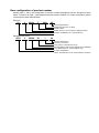
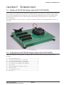
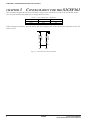
MF1466-01
CMOS 8-BIT SINGLE CHIP MICROCOMPUTER
S5U1C8F360Z1 Manual
(Adapter Board for S1C8F360/8F361)
NOTICE
No part of this material may be reproduced or duplicated in any form or by any means without the written permission of Seiko
Epson. Seiko Epson reserves the right to make changes to this material without notice. Seiko Epson does not assume any
liability of any kind arising out of any inaccuracies contained in this material or due to its application or use in any product or
circuit and, further, there is no representation that this material is applicable to products requiring high level reliability, such
as medical products. Moreover, no license to any intellectual property rights is granted by implication or otherwise, and there
is no representation or warranty that anything made in accordance with this material will be free from any patent or copyright
infringement of a third party. This material or portions thereof may contain technology or the subject relating to strategic
products under the control of the Foreign Exchange and Foreign Trade Law of Japan and may require an export license from
the Ministry of International Trade and Industry or other approval from another government agency.
© SEIKO EPSON CORPORATION 2001 All rights reserved.
New configuration of product number
Starting April 1, 2001, the configuration of product number descriptions will be changed as listed
below. To order from April 1, 2001 please use these product numbers. For further information, please
contact Epson sales representative.
Devices
S1
C
88104
F
0A01
00
Packing specification
Package (D: die form; F: QFP)
Model number
Model name (C: microcomputer, digital products)
Product classification (S1: semiconductor)
Development tools
C
88348
S5U1
D1
1
00
Packing specification
Version (1: Version 1)
Tool type (D1: Development Tool)
Corresponding model number (88348: for S1C88348)
Tool classification (C: microcomputer use)
Product classification
(S5U1: development tool for semiconductor products)
CONTENTS
S5U1C8F360Z1 Manual (Adapter Board for S1C8F360/8F361)
This manual describes how to use the Adapter Board (S5U1C8F360Z1) that is a PROM writing and
evaluation tool for the 8-bit Single Chip Microcomputer S1C8F360/8F361.
Contents
CHAPTER
1 INTRODUCTION ____________________________________________ 1
1.1
1.2
CHAPTER
Outline of S1C8F360 Adapter Board (S5U1C8F360Z1) ............................. 1
Components of S1C8F360 Adapter Board (S5U1C8F360Z1) ..................... 1
2 PRECAUTIONS ____________________________________________ 2
2.1
2.2
Precautions for Operation ............................................................................ 2
Differences from the ICE88UR (S5U1C88000H5)
+ PRC88816 (S5U1C88816P) ..................................................................... 2
CHAPTER
3 CONFIGURATION FOR THE S1C8F361 __________________________ 4
CHAPTER
4 NAME AND FUNCTION OF EACH PART ___________________________ 5
CHAPTER
5 SERIAL PROGRAMMING ______________________________________ 6
5.1
5.2
5.3
Setting the Jumpers ....................................................................................... 6
Connecting the Power Cable ........................................................................ 6
Pin Assignment of the CN4 Connector for Serial Programming ................. 6
CHAPTER
6 CONNECTING WITH THE TARGET SYSTEM _________________________ 7
CHAPTER
7 S1C8F360 ADAPTER BOARD (S5U1C8F360Z1) SCHEMATIC DIAGRAM _ 9
CHAPTER
8 PRODUCT SPECIFICATIONS ___________________________________ 10
S5U1C8F360Z1 MANUAL
(ADAPTER BOARD FOR S1C8F360/8F361)
EPSON
i
CHAPTER 1: INTRODUCTION
CHAPTER 1
INTRODUCTION
1.1 Outline of S1C8F360 Adapter Board (S5U1C8F360Z1)
The S5U1C8F360Z1 board (hereafter Adapter Board) is a PROM writing tool for the 8-bit Single Chip
Microcomputers S1C8F360 and S1C8F361. The Adapter Board connected to the On Board Programming
Writer (S5U1C88000W3) allows writing user data to the Flash EEPROM built into the S1C8F360/8F361
(package model) placed on its IC socket using the On Board Programming Writer Control Software
(S5U1C8F360Y3).
The Adapter Board can also be used as a software evaluation board by mounting peripheral circuits on
the board.
S5U1C8F360Z1
1.2 Components of S1C8F360 Adapter Board (S5U1C8F360Z1)
After unpacking the S5U1C8F360Z1 package, check to see that all of the following components are
included.
(1)
(2)
(3)
(4)
(5)
(6)
(7)
(8)
(9)
(10)
S5U1C8F360Z1 board ................................................................
I/O cable (80-pin/40-pin × 2 flat type) ..................................
I/O cable (60-pin/30-pin × 2 flat type) ..................................
I/O connector for target system (40 pins) .............................
I/O connector for target system (30 pins) .............................
Power cable .................................................................................
S5U1C8F360Z1 Manual (this manual) ...................................
Warranty card .............................................................................
User registration card ...............................................................
Note for use ................................................................................
S5U1C8F360Z1 MANUAL
(ADAPTER BOARD FOR S1C8F360/8F361)
EPSON
1
2
1
4
2
1
1
1
1
1
1
CHAPTER 2: PRECAUTIONS
CHAPTER 2
PRECAUTIONS
The connectors CN1, CN2 and CN3 have the same pin layout as the Peripheral Circuit Board for
S1C88816/8F360 (S5U1C88816P). This allows connection between the user target system for the
S5U1C88816P and the Adapter Board.
Take the following precautions when using the S1C8F360 Adapter Board (S5U1C8F360Z1):
2.1 Precautions for Operation
(1) Turn the power of all equipment off before connecting or disconnecting cables.
(2) Do not turn the power on while the input ports (K00–K03) are all set to low level. It may cause a
simultaneous key input reset.
2.2 Differences from the ICE88UR (S5U1C88000H5)
+ PRC88816 (S5U1C88816P)
The emulation system using the Adapter Board with an actual IC differs in terms of functionality and
characteristics from the S5U1C88816P emulation system, a fact which requires your attention. If these
differences are ignored, there is a possibility that your circuit will not operate properly on an actual IC
even though it might have performed well on the S5U1C88000H5 with the S5U1C88816P.
(1) Power supply differences
To operate the actual IC on the Adapter Board, an external power source voltage must be applied.
Refer to "Electrical Characteristics" chapter in the "S1C8F360 Technical Manual" for the supply
voltage.
(2) I/O differences
The output drive capability and pull up resistance are different.
The input setup time is different therefore, when a circuit requiring consideration of the input response time, such as a key matrix, is used, the system and the software should be designed according
to the specifications for the actual IC.
(3) LCD differences
The output drive capability is different.
Since there will be differences with the actual IC even for the drive voltage, the system and the
software should be designed in order to adjust the characteristics.
(4) Analog comparator differences
The response time and characteristics of the analog comparator are different. Consequently, the
system and the software should be designed according to the specifications for the actual IC.
(5) Functional differences
<Oscillation circuit>
• The Adapter Board does not contain oscillator parts. Mount the parts according to the selected mask
option for the actual IC.
• The OSC3 oscillation stability time of the S5U1C88816P is shorter than that of the actual IC. Therefore, the application program must take enough of interval (more than the oscillation stability time
in the actual IC) between starting the OSC3 oscillation and switching the system clock to OSC3.
• The logic level is different and it makes different oscillation timings such as the start and stop times.
• When switching the operating clock from OSC3 to OSC1, be sure to switch OSC3 oscillation off with
separate instructions. Using a single instruction to process simultaneously may cause a malfunction
of the CPU.
2
EPSON
S5U1C8F360Z1 MANUAL
(ADAPTER BOARD FOR S1C8F360/8F361)
CHAPTER 2: PRECAUTIONS
• Do not turn the OSC3 oscillation circuit on in the low power mode.
Do not switch over the operating mode (normal mode ↔ high speed mode) when the OSC3 oscillation circuit is on, as this will cause a malfunction.
<Internal power supply circuit>
The actual IC on the Adapter Board can change over the internal power voltage (set by VDC2, VDC1
and VDC0), but the S5U1C88816P cannot change the actual power voltage, because only the VDC2,
VDC1 and VDC0 values are changed.
For this reason, since the S5U1C88816P will operate, even if the stable time required for changeover is
not taken, be sure that the stable time is provided by the software.
Also, since the usable frequency of OSC1 and OSC3 depends on the internal power voltage, refer to
the technical manual for the S1C8F360 or S1C8F361 and take care so as not to operate it with an
inappropriate combination.
When turning the OSC3 oscillation circuit on after switching the operating voltage, the software must
take a voltage stabilization wait time of 5 msec.
<LCD drive power>
To drive an LCD using the Adapter Board, mount the parts required for VC1 to VC5 and CA to CE (CA
to CG in the S1C8F361) on the board or supply an external LCD power.
Note: The S1C8F360 Adapter Board supports the S1C8F361 as well. When using the board for the
S1C8F361, the AVDD and AVSS pins on the board must be changed to the CF and CG pins,
respectively, using the jumper and mount a capacitor to the holes indicated as C1.
<Reset circuit>
___________
Mount parts such as a switch and a capacitor at the RESET pin on the Adapter Board.
S5U1C8F360Z1 MANUAL
(ADAPTER BOARD FOR S1C8F360/8F361)
EPSON
3
CHAPTER 3: CONFIGURATION FOR THE S1C8F361
CHAPTER 3
CONFIGURATION FOR THE S1C8F361
The S1C8F360 Adapter Board (S5U1C8F360Z1) supports the S1C8F361 as well as the S1C8F360. In this
case, the pins listed in the table below change their functions.
Table 3.1 Pin function for S1C8F361
Print
AVDD
AVSS
S1C8F360
AVDD
AVSS
S1C8F361
CF
CG
AVSS
AVDD
When using the S1C8F361, open the AVDD and AVSS jumpers and mount the booster capacitor for the CF
and CG at C1.
C1
CF
CG
Fig. 3.1 CF and CG for the S1C8F361
4
EPSON
S5U1C8F360Z1 MANUAL
(ADAPTER BOARD FOR S1C8F360/8F361)
CHAPTER 4: NAME AND FUNCTION OF EACH PART
CHAPTER 4
NAME AND FUNCTION OF EACH PART
This chapter describes the name and function of each part of the S1C8F360 Adapter Board
(S5U1C8F360Z1).
(5)
(4)
(3)
(1)
(2)
(6)
(2)
(2)
(7)
Fig. 4.1 Top view of the S5U1C8F360Z1 board
(1) IC socket
Insert an actual IC. Align Pin 1 with the bottom left corner of the socket (in top view) and insert IC.
(2) Connectors for target system (CN1, CN2, CN3)
These connectors are used to connect the I/O and LCD. Connect the target system using the I/O
cables (80-pin/40-pin × 2 flat type and 60-pin/30-pin × 2 flat type).
The pin assignment is the same as the S5U1C88816P connectors.
Refer to Chapter 6, "Connecting with the Target System", for the pin assignment.
(3) Connector for serial programming (CN4)
This connector is used to connect the On Board Programming Writer (S5U1C88000W3). Use this
connector when writing user data to the Flash EEPROM built into the microcomputer on the IC slot.
Refer to Chapter 5, "Serial Programming", for the pin assignment. For how to use the On Board
Programming Writer, refer to the "S1C8F360 Technical Manual".
(4) Power connector (CN5)
This connector is used to supply power to the S1C8F360 Adapter Board.
Use the supplied power cable for connection.
(5) Power system jumpers and check pins
Set according to the power supply conditions.
(6) Through holes for oscillator, LCD drive power and LCD voltage booster
Use them to mount the parts such as oscillator parts, capacitors and resistors. Refer to "Basic External
Wiring Diagram" in the "S1C8F360 Technical Manual" for the basic parts to be mounted.
(7) IC socket pattern
Cannot be used.
S5U1C8F360Z1 MANUAL
(ADAPTER BOARD FOR S1C8F360/8F361)
EPSON
5
CHAPTER 5: SERIAL PROGRAMMING
CHAPTER 5
SERIAL PROGRAMMING
The S1C8F360 Adapter Board (S5U1C8F360Z1) connected to the On Board Programming Writer
(S5U1C88000W3) allows writing user data to the Flash EEPROM built into the S1C8F360/8F361 (package
model) placed on its IC socket using the On Board Programming Writer Control Software
(S5U1C8F360Y3).
Refer to "Appendix PROM programming" in the "S1C8F360 Technical Manual" for the programming
procedure.
5.1 Setting the Jumpers
Before performing serial programming, set the jumpers for the power unit as shown in Table 5.1.1.
Note: Be aware that the configuration is different between the S1C8F360 and the S1C8F361.
Table 5.1.1 Jumper settings for serial programming
Jumper
VDD
VSS
AVDD
AVSS
AVREF
S1C8F360
short
short
short
short
short
S1C8F361
short
short
open
open
short
5.2 Connecting the Power Cable
Serial programming needs external power to be supplied to the CN5 connector on the S1C8F360 Adapter
Board (S5U1C8F360Z1) using the supplied power cable.
Table 5.2.1 Pin assignment of the CN5 power connector
CN5
1
2
Power cable
Red
Black
Power supply
VDD
VSS
5.3 Pin Assignment of the CN4 Connector for Serial Programming
The CN4 connector is used to connect the SIO cable from the On Board Programming Writer
(S5U1C88000W3).
Table 5.3.1 Pin assignment of the CN4 connector for serial programming
CN4
No. Pin name
1
VD1F
2
VDD
CLKW
3
VSS
4
SCLK
5
VSS
6
TXD
7
VSS
8
RXD
9
VSS
10
RESET
11
VSS
12
SPRG
13
VSS
14
N.C.
15
N.C.
16
6
Function
Programming power supply pin
Power supply pin
System clock output pin
GND pin
Serial I/F clock output pin
GND pin
Serial I/F data output pin
GND pin
Serial I/F data input pin
GND pin
Initial reset output pin
GND pin
Programming mode setup output pin
GND pin
EPSON
S5U1C8F360Z1 MANUAL
(ADAPTER BOARD FOR S1C8F360/8F361)
CHAPTER 6: CONNECTING WITH THE TARGET SYSTEM
CHAPTER 6
CONNECTING WITH THE TARGET SYSTEM
The Adapter Board (S5U1C8F360Z1) can be used as an evaluation board by connecting it with the user
target board.
(1) To operate the microcomputer on the Adapter Board, the user must provide the peripheral circuits.
Refer to "Basic External Wiring Diagram" in the "S1C8F360 Technical Manual" for the required circuits.
(2) Use the supplied I/O cables (80-pin/40-pin × 2 flat type and 60-pin/30-pin × 2 flat type) for connecting between the S1C8F360 Adapter Board (S5U1C8F360Z1) and the target system.
(3) Be sure to turn the power off before connecting the target system because the I/O cable includes a
power line (VDD).
I/O cables
CN1-1
(40 pins)
CN1-2
(40 pins)
CN2-1
(40 pins)
CN2-2
(40 pins)
mark
CN1
CN3-1
To target board
(30 pins)
CN2
CN3-2
(30 pins)
CN3
Fig. 6.1 Connecting with the target system
S5U1C8F360Z1 MANUAL
(ADAPTER BOARD FOR S1C8F360/8F361)
EPSON
7
CHAPTER 6: CONNECTING WITH THE TARGET SYSTEM
Table 6.1 Pin assignment of the I/O connectors
CN1
40-pin CN1-1
40-pin CN1-2
No. Pin name No. Pin name
1
VDD
1
R12
2
2
R13
VDD
3
VSS
3
R14
4
VSS
4
R15
5
5
R16
K00
6
6
R17
K01
7
7
R20
K02
8
8
R21
K03
9
9
R22
K04
10
10
R23
K05
11
11
R24
K06
12
12
R25
K07
13
13
R26
K10
14
14
R27
K11
15
15
R30
P00
16
16
R31
P01
17
17
R32
P02
18
18
R33
P03
19
19
R34
P04
20
20
R35
P05
21
21
R36
P06
22
22
R37
P07
23
23
R50
P10
24
24
R51
P11
25
25
COM0
P12
26
26
COM1
P13
27
27
COM2
P14
28
28
COM3
P15
29
29
COM4
P16
30
30
COM5
P17
31
31
COM6
R00
32
32
COM7
R01
33
33
COM8
R02
34
34
COM9
R03
35
35
COM10
R04
36
36
COM11
R05
37
37
COM12
R06
38
38
COM13
R07
39
39
COM14
R10
40
40
COM15
R11
8
CN2
40-pin CN2-1
40-pin CN2-2
No. Pin name No. Pin name
1
VDD
1
SEG27
2
2
SEG28
VDD
3
VSS
3
SEG29
4
VSS
4
SEG30
5
5
SEG31
RESET
6 MCU/MPU 6
SEG32
7
7
SEG33
OSC1
8
8
SEG34
OSC3
9
9
SEG35
VC1
10
VC2
10
SEG36
11
11
SEG37
VC3
12
VC4
12
SEG38
13
VC5
13
SEG39
14
SEG0
14
SEG40
15
SEG1
15
SEG41
16
SEG2
16
SEG42
17
SEG3
17
SEG43
18
SEG4
18
SEG44
19
SEG5
19
SEG45
20
SEG6
20
SEG46
21
SEG7
21
SEG47
22
SEG8
22
SEG48
23
SEG9
23
SEG49
24
SEG10
24
SEG50
25
SEG11
25
COM31
26
SEG12
26
COM30
27
SEG13
27
COM29
28
SEG14
28
COM28
29
SEG15
29
COM27
30
SEG16
30
COM26
31
SEG17
31
COM25
32
SEG18
32
COM24
33
SEG19
33
COM23
34
SEG20
34
COM22
35
SEG21
35
COM21
36
SEG22
36
COM20
37
SEG23
37
COM19
38
SEG24
38
COM18
39
SEG25
39
COM17
40
SEG26
40
COM16
EPSON
CN3
30-pin CN3-1
30-pin CN3-2
No. Pin name No. Pin name
1
SEG51
1
N.C.
2
SEG52
2
N.C.
3
SEG53
3
N.C.
4
SEG54
4
N.C.
5
SEG55
5
N.C.
6
SEG56
6
N.C.
7
SEG57
7
N.C.
8
SEG58
8
N.C.
9
SEG59
9
N.C.
10
SEG60
10
N.C.
11
SEG61
11
N.C.
12
SEG62
12
N.C.
13
SEG63
13
N.C.
14
SEG64
14
N.C.
15
SEG65
15
N.C.
16
SEG66
16
N.C.
17
N.C.
17
N.C.
18
N.C.
18
N.C.
19
N.C.
19
N.C.
20
N.C.
20
N.C.
21
N.C.
21
N.C.
22
N.C.
22
N.C.
23
N.C.
23
N.C.
24
N.C.
24
N.C.
25
N.C.
25
N.C.
26
N.C.
26
N.C.
27
N.C.
27
N.C.
28
N.C.
28
N.C.
29
N.C.
29
N.C.
30
N.C.
30
N.C.
S5U1C8F360Z1 MANUAL
(ADAPTER BOARD FOR S1C8F360/8F361)
41
42
43
44
45
46
47
48
49
50
51
52
53
54
55
56
57
58
59
60
61
62
63
64
65
66
67
68
69
70
71
72
73
74
75
76
77
78
79
80
R12
R13
R14
R15
R16
R17
R20
R21
R22
R23
R24
R25
R26
R27
R30
R31
R32
R33
R34
R35
R36
R37
R50
R51
COM0
COM1
COM2
COM3
COM4
COM5
COM6
COM7
COM8
COM9
COM10
COM11
COM12
COM13
COM14
COM15
1
2
3
4
5
6
7
8
9
10
11
12
13
14
15
16
17
18
19
20
21
22
23
24
25
26
27
28
29
30
31
32
33
34
35
36
37
38
39
40
2-1
2-2
2-3
2-4
2-5
2-6
2-7
2-8
2-9
2-10
2-11
2-12
2-13
2-14
2-15
2-16
2-17
2-18
2-19
2-20
2-21
2-22
2-23
2-24
2-25
2-26
2-27
2-28
2-29
2-30
2-31
2-32
2-33
2-34
2-35
2-36
2-37
2-38
2-39
2-40
41
42
43
44
45
46
47
48
49
50
51
52
53
54
55
56
57
58
59
60
61
62
63
64
65
66
67
68
69
70
71
72
73
74
75
76
77
78
79
80
SEG27
SEG28
SEG29
SEG30
SEG31
SEG32
SEG33
SEG34
SEG35
SEG36
SEG37
SEG38
SEG39
SEG40
SEG41
SEG42
SEG43
SEG44
SEG45
SEG46
SEG47
SEG48
SEG49
SEG50
COM31
COM30
COM29
COM28
COM27
COM26
COM25
COM24
COM23
COM22
COM21
COM20
COM19
COM18
COM17
COM16
1
2
3
4
5
6
7
8
9
10
11
12
13
14
15
16
17
18
19
20
21
22
23
24
25
26
27
28
29
30
CN4
S5U1C8F360Z1 MANUAL
(ADAPTER BOARD FOR S1C8F360/8F361)
EPSON
VD1F
VDD
CLKW
GND
SCLK
GND
TXD
GND
RXD
GND
XRESET
GND
XSPRG
GND
31
32
33
34
35
36
37
38
39
40
41
42
43
44
45
46
47
48
49
50
51
52
53
54
55
56
57
58
59
60
4
VDD
1
2
3
4
5
6
7
8
9
10
11
12
13
14
15
16
2-1
2-2
2-3
2-4
2-5
2-6
2-7
2-8
2-9
2-10
2-11
2-12
2-13
2-14
2-15
2-16
2-17
2-18
2-19
2-20
2-21
2-22
2-23
2-24
2-25
2-26
2-27
2-28
2-29
2-30
VSS
1-1
1-2
1-3
1-4
1-5
1-6
1-7
1-8
1-9
1-10
1-11
1-12
1-13
1-14
1-15
1-16
1-17
1-18
1-19
1-20
1-21
1-22
1-23
1-24
1-25
1-26
1-27
1-28
1-29
1-30
CN3
R11
R12
R13
R14
R15
R16
R17
R20
R21
R22
R23
R24
R25
R26
R27
R30
R31
R32
R33
R34
R35
R36
R37
VSS
R50
R51
COM0
COM1
COM2
COM3
COM4
COM5
COM6
COM7
COM8
COM9
COM10
COM11
COM12
COM13
COM14
COM15
SEG0
SEG1
AVDD/CF
133
134
135
136
137
138
139
140
141
142
143
144
145
146
147
148
149
150
151
152
153
154
155
156
157
158
159
160
161
162
163
164
165
166
167
168
169
170
171
172
173
174
175
176
AVSS/CG
3
SEG51
SEG52
SEG53
SEG54
SEG55
SEG56
SEG57
SEG58
SEG59
SEG60
SEG61
SEG62
SEG63
SEG64
SEG65
SEG66
R11
R12
R13
R14
R15
R16
R17
R20
R21
R22
R23
R24
R25
R26
R27
R30
R31
R32
R33
R34
R35
R36
R37
VSS
R50
R51
COM0
COM1
COM2
COM3
COM4
COM5
COM6
COM7
COM8
COM9
COM10
COM11
COM12
COM13
COM14
COM15
SEG0
SEG1
AVSS/CG
JP4
AVREF
JP5
AVREF
1-1
1-2
1-3
1-4
1-5
1-6
1-7
1-8
1-9
1-10
1-11
1-12
1-13
1-14
1-15
1-16
1-17
1-18
1-19
1-20
1-21
1-22
1-23
1-24
1-25
1-26
1-27
1-28
1-29
1-30
1-31
1-32
1-33
1-34
1-35
1-36
1-37
1-38
1-39
1-40
C1
AVDD/CF
JP3
VOSC
VOSC
VOSC
VD1
VD1
VD1F
OSC1
OSC2
/TEST
/RESET
MCU/MPU
K11
K10
K07
K06
K05
K04
K03
K02
K01
K00
P17
P16
P15
P14
P13
P12
P11
P10
AVDD
AVSS
AVREF
VDD
P07
P06
P05
P04
P03
P02
P01
P00
R00
R01
R02
R03
R04
R05
R06
R07
R10
SEG45
SEG44
SEG43
SEG42
SEG41
SEG40
SEG39
SEG38
SEG37
SEG36
SEG35
SEG34
SEG33
SEG32
SEG31
SEG30
SEG29
SEG28
SEG27
SEG26
SEG25
SEG24
SEG23
SEG22
SEG21
SEG20
SEG19
SEG18
SEG17
SEG16
SEG15
SEG14
SEG13
SEG12
SEG11
SEG10
SEG9
SEG8
SEG7
SEG6
SEG5
SEG4
SEG3
SEG2
44
43
42
41
40
39
38
37
36
35
34
33
32
31
30
29
28
27
26
25
24
23
22
21
20
19
18
17
16
15
14
13
12
11
10
9
8
7
6
5
4
3
2
1
2
VDD
VDD
VSS
VSS
XRESET
MCU/MPU
OSC1
OSC3
VC1
VC2
VC3
VC4
VC5
SEG0
SEG1
SEG2
SEG3
SEG4
SEG5
SEG6
SEG7
SEG8
SEG9
SEG10
SEG11
SEG12
SEG13
SEG14
SEG15
SEG16
SEG17
SEG18
SEG19
SEG20
SEG21
SEG22
SEG23
SEG24
SEG25
SEG26
VSS
6
VD1
89
90
91
92
93
94
95
96
97
98
99
100
101
102
103
104
105
106
107
108
109
110
111
112
113
114
115
116
117
118
119
120
121
122
123
124
125
126
127
128
129
130
131
132
1
2-1
2-2
2-3
2-4
2-5
2-6
2-7
2-8
2-9
2-10
2-11
2-12
2-13
2-14
2-15
2-16
2-17
2-18
2-19
2-20
2-21
2-22
2-23
2-24
2-25
2-26
2-27
2-28
2-29
2-30
2-31
2-32
2-33
2-34
2-35
2-36
2-37
2-38
2-39
2-40
VCC
JP2
GND
VDD
VCC
JP1
5
GND
VD1F
OSC1
OSC2
XTEST
XRESET
MCU/MPU
K11
K10
K07
K06
K05
K04
K03
K02
K01
K00
P17
P16
P15
P14
P13
P12
P11
P10
AVDD/CF
AVSS/CG
AVREF
VDD
P07
P06
P05
P04
P03
P02
P01
P00
R00
R01
R02
R03
R04
R05
R06
R07
R10
1-1
1-2
1-3
1-4
1-5
1-6
1-7
1-8
1-9
1-10
1-11
1-12
1-13
1-14
1-15
1-16
1-17
1-18
1-19
1-20
1-21
1-22
1-23
1-24
1-25
1-26
1-27
1-28
1-29
1-30
1-31
1-32
1-33
1-34
1-35
1-36
1-37
1-38
1-39
1-40
4
OSC1
OSC2
A
1
2
3
4
5
6
7
8
9
10
11
12
13
14
15
16
17
18
19
20
21
22
23
24
25
26
27
28
29
30
31
32
33
34
35
36
37
38
39
40
CN2
3
VCC
XTEST
K00
K01
K02
K03
K04
K05
K06
K07
K10
K11
MCU/MPU
XTEST
XSPRG
XSPRG
XRESET
XRESET
5
6
SEG44
SEG43
SEG42
SEG41
SEG40
SEG39
SEG38
SEG37
SEG36
SEG35
SEG34
SEG33
SEG32
SEG31
SEG30
SEG29
SEG28
SEG27
SEG26
SEG25
SEG24
SEG23
SEG22
SEG21
SEG20
SEG19
SEG18
SEG17
SEG16
SEG15
SEG14
SEG13
SEG12
SEG11
SEG10
SEG9
SEG8
SEG7
SEG6
SEG5
SEG4
SEG3
SEG2
K11 K10 K07 K06 K05 K04 K03 K02 K01 K00
MCU/MPU
VOSC
VSS
VDD
VD1
OSC4
OSC3
VC1
VC2
VC3
VC4
VC5
CA
CB
CC
CD
CE
TXD
SCLK
RXD
VEPEXT
CLKW
XSPRG
VD1F
COM16
COM17
COM18
COM19
COM20
COM21
COM22
COM23
COM24
COM25
COM26
COM27
COM28
COM29
COM30
COM32
SEG50
SEG49
SEG48
SEG47
SEG46
XTAL1
CG1
7
88
87
86
85
84
83
82
81
80
79
78
77
76
75
74
73
72
71
70
69
68
67
66
65
64
63
62
61
60
59
58
57
56
55
54
53
52
51
50
49
48
47
46
45
VOSC
VSS
VDD
VD1
OSC4
OSC3
VC1
VC2
VC3
VC4
VC5
CA
CB
CC
CD
CE
TXD
SCLK
RXD
VEPEXT
CLKW
XSPRG
VD1F
COM16
COM17
COM18
COM19
COM20
COM21
COM22
COM23
COM24
COM25
COM26
COM27
COM28
COM29
COM30
COM31
SEG50
SEG49
SEG48
SEG47
SEG46
U1
S1C8F360
7
VEPEXT
CE
OSC4
OSC3
VC1
VC2
VC3
VC4
VC5
CA
CB
CC
CD
VSS
VDD
XTAL2
Rf
VCC
GND
VEPEXT
CD
CA
CC
CE
CA
CB
Cp
1
2
CN5
8
CG2
CD2
8
R1
VC5
VC4
VC3
VC2
VC1
2
B
VDD
VDD
VSS
VSS
K00
K01
K02
K03
K04
K05
K06
K07
K10
K11
P00
P01
P02
P03
P04
P05
P06
P07
P10
P11
P12
P13
P14
P15
P16
P17
P20
P21
P22
P23
P24
P25
P26
P27
R10
R11
CN1
2
1
C
D
1
A
B
C
D
CHAPTER 7: S1C8F360 ADAPTER BOARD (S5U1C8F360Z1) SCHEMATIC DIAGRAM
CHAPTER 7
S1C8F360 ADAPTER BOARD
(S5U1C8F360Z1) SCHEMATIC DIAGRAM
9
CHAPTER 8: PRODUCT SPECIFICATIONS
CHAPTER
8 PRODUCT SPECIFICATIONS
The component specifications of the S1C8F360 Adapter Board (S5U1C8F360Z1) are listed below.
S5U1C8F360Z1
Dimensions:
183 mm (L) × 154 mm (W) × 48 mm (H)
Power supply:
Within the operating voltage range of the microcomputer
I/O cable (80-pin/40-pin × 2, 2 sets)
S5U1C8F360Z1 connector:
KEL 8830-80-170L or equivalent
Cable connector (80-pin):
KEL 8822E-080-171
Cable connector (40-pin):
3M 7940-6500SC
Cable:
40-pin flat cable
Length:
Approx. 40 cm
×1/1 set
×2/1 set
×2/1 set
(both cables are the same length)
I/O connection cable (60-pin/30-pin × 2, 1 set)
S5U1C8F360Z1 connector:
KEL 8830-60-170
Cable connector (60-pin):
KEL 8822E-060-171
×1/1 set
Cable connector (30-pin):
3M 7930-6500SC
×2/1 set
Cable:
30-pin flat cable
×2/1 set
Length:
Approx. 40 cm
Power cable
S5U1C8F360Z1 connector:
J.S.T. Mfg Co., Ltd B2B-XH-A
Cable connector:
J.S.T. Mfg Co., Ltd XHP-2
Contacts:
J.S.T. Mfg Co., Ltd SXH-001T-P0.6
Length:
Approx. 35 cm
Accessories
I/O connectors for the target system
(40-pin): 3M 3432-6002LCSC
(30-pin): 3M 3440-6002LCSC
×4
×2
10
EPSON
S5U1C8F360Z1 MANUAL
(ADAPTER BOARD FOR S1C8F360/8F361)
International Sales Operations
AMERICA
ASIA
EPSON ELECTRONICS AMERICA, INC.
EPSON (CHINA) CO., LTD.
- HEADQUARTERS -
23F, Beijing Silver Tower 2# North RD DongSanHuan
ChaoYang District, Beijing, CHINA
Phone: 64106655
Fax: 64107319
150 River Oaks Parkway
San Jose, CA 95134, U.S.A.
Phone: +1-408-922-0200
Fax: +1-408-922-0238
SHANGHAI BRANCH
4F, Bldg., 27, No. 69, Gui Jing Road
Caohejing, Shanghai, CHINA
Phone: 21-6485-5552
Fax: 21-6485-0775
- SALES OFFICES West
1960 E. Grand Avenue
EI Segundo, CA 90245, U.S.A.
Phone: +1-310-955-5300
Fax: +1-310-955-5400
Central
101 Virginia Street, Suite 290
Crystal Lake, IL 60014, U.S.A.
Phone: +1-815-455-7630
Fax: +1-815-455-7633
Northeast
301 Edgewater Place, Suite 120
Wakefield, MA 01880, U.S.A.
Phone: +1-781-246-3600
Fax: +1-781-246-5443
EPSON HONG KONG LTD.
20/F., Harbour Centre, 25 Harbour Road
Wanchai, Hong Kong
Phone: +852-2585-4600 Fax: +852-2827-4346
Telex: 65542 EPSCO HX
EPSON TAIWAN TECHNOLOGY & TRADING LTD.
10F, No. 287, Nanking East Road, Sec. 3
Taipei
Phone: 02-2717-7360
Fax: 02-2712-9164
Telex: 24444 EPSONTB
HSINCHU OFFICE
Southeast
3010 Royal Blvd. South, Suite 170
Alpharetta, GA 30005, U.S.A.
Phone: +1-877-EEA-0020 Fax: +1-770-777-2637
13F-3, No. 295, Kuang-Fu Road, Sec. 2
HsinChu 300
Phone: 03-573-9900
Fax: 03-573-9169
EPSON SINGAPORE PTE., LTD.
No. 1 Temasek Avenue, #36-00
Millenia Tower, SINGAPORE 039192
Phone: +65-337-7911
Fax: +65-334-2716
EUROPE
EPSON EUROPE ELECTRONICS GmbH
SEIKO EPSON CORPORATION KOREA OFFICE
- HEADQUARTERS Riesstrasse 15
80992 Munich, GERMANY
Phone: +49-(0)89-14005-0
Fax: +49-(0)89-14005-110
SALES OFFICE
Altstadtstrasse 176
51379 Leverkusen, GERMANY
Phone: +49-(0)2171-5045-0
Fax: +49-(0)2171-5045-10
UK BRANCH OFFICE
Unit 2.4, Doncastle House, Doncastle Road
Bracknell, Berkshire RG12 8PE, ENGLAND
Phone: +44-(0)1344-381700
Fax: +44-(0)1344-381701
50F, KLI 63 Bldg., 60 Yoido-dong
Youngdeungpo-Ku, Seoul, 150-763, KOREA
Phone: 02-784-6027
Fax: 02-767-3677
SEIKO EPSON CORPORATION
ELECTRONIC DEVICES MARKETING DIVISION
Electronic Device Marketing Department
IC Marketing & Engineering Group
421-8, Hino, Hino-shi, Tokyo 191-8501, JAPAN
Phone: +81-(0)42-587-5816
Fax: +81-(0)42-587-5624
ED International Marketing Department Europe & U.S.A.
FRENCH BRANCH OFFICE
1 Avenue de l' Atlantique, LP 915 Les Conquerants
Z.A. de Courtaboeuf 2, F-91976 Les Ulis Cedex, FRANCE
Phone: +33-(0)1-64862350
Fax: +33-(0)1-64862355
BARCELONA BRANCH OFFICE
Barcelona Design Center
Edificio Testa, Avda. Alcalde Barrils num. 64-68
E-08190 Sant Cugat del Vallès, SPAIN
Phone: +34-93-544-2490
Fax: +34-93-544-2491
421-8, Hino, Hino-shi, Tokyo 191-8501, JAPAN
Phone: +81-(0)42-587-5812
Fax: +81-(0)42-587-5564
ED International Marketing Department Asia
421-8, Hino, Hino-shi, Tokyo 191-8501, JAPAN
Phone: +81-(0)42-587-5814
Fax: +81-(0)42-587-5110
In pursuit of “Saving” Technology, Epson electronic devices.
Our lineup of semiconductors, liquid crystal displays and quartz devices
assists in creating the products of our customers’ dreams.
Epson IS energy savings.
S5U1C8F360Z1 Manual
(Adapter Board for S1C8F360/8F361)
ELECTRONIC DEVICES MARKETING DIVISION
EPSON Electronic Devices Website
http://www.epson.co.jp/device/
Issue July, 2001
Printed in Japan L A