1
MELSEC-Q Current Transformer Input Module
User's Manual
-Q68CT
SAFETY PRECAUTIONS
(Read these precautions before using this product.)
Before using this product, please read this manual and the relevant manuals carefully and pay full attention
to safety to handle the product correctly.
The precautions given in this manual are concerned with this product only. For the safety precautions of the
programmable controller system, refer to the user's manual for the CPU module used.
In this manual, the safety precautions are classified into two levels: "
WARNING" and "
CAUTION".
WARNING
Indicates that incorrect handling may cause hazardous conditions,
resulting in death or severe injury.
CAUTION
Indicates that incorrect handling may cause hazardous conditions,
resulting in minor or moderate injury or property damage.
Under some circumstances, failure to observe the precautions given under "
CAUTION" may lead to
serious consequences.
Observe the precautions of both levels because they are important for personal and system safety.
Make sure that the end users read this manual and then keep the manual in a safe place for future
reference.
[Design Precautions]
WARNING
● Do not write any data to the "system area" and "write-protect area" of the buffer memory in the
intelligent function module. Also, do not use any "use prohibited" signal as an output signal from the
CPU module to the intelligent function module. Doing so may cause malfunction of the programmable
controller system.
CAUTION
● Do not install the control lines or communication cables together with the main circuit lines or power
cables. Failure to do so may result in malfunction due to noise.
1
[Installation Precautions]
CAUTION
● Use the programmable controller in an environment that meets the general specifications in the user's
manual for the CPU module used. Failure to do so may result in electric shock, fire, malfunction, or
damage to or deterioration of the product.
● To mount the module, while pressing the module mounting lever located in the lower part of the
module, fully insert the module fixing projection(s) into the hole(s) in the base unit and press the
module until it snaps into place. Incorrect interconnection may cause malfunction, failure, or drop of
the module. When using the programmable controller in an environment of frequent vibrations, fix the
module with a screw. Tighten the screws within the specified torque range. Undertightening can cause
drop of the screw, short circuit, or malfunction. Overtightening can damage the screw and/or module,
resulting in drop, short circuit, or malfunction.
● Shut off the external power supply (all phases) used in the system before mounting or removing the
module. Failure to do so may result in damage to the product. A module can be replaced online (while
power is on) on any MELSECNET/H remote I/O station or in the system where a CPU module
supporting the online module change function is used. Note that there are restrictions on the modules
that can be replaced online, and each module has its predetermined replacement procedure. For
details, refer to the relevant chapter in this manual.
● Do not directly touch any conductive parts and electronic components of the module. Doing so can
cause malfunction or failure of the module.
[Wiring Precautions]
WARNING
● After installation and wiring, attach the included terminal cover to the module before turning it on for
operation. Failure to do so may result in electric shock.
CAUTION
● Individually ground the FG terminal of the programmable controller with a ground resistance of 100Ω
or less. Failure to do so may result in electric shock or malfunction.
● Tighten the terminal screws within the specified torque range. Undertightening can cause short circuit,
fire, or malfunction. Overtightening can damage the screw and/or module, resulting in drop, short
circuit, or malfunction.
● Prevent foreign matter such as dust or wire chips from entering the module. Such foreign matter can
cause a fire, failure, or malfunction.
● A protective film is attached to the top of the module to prevent foreign matter, such as wire chips,
from entering the module during wiring. Do not remove the film during wiring. Remove it for heat
dissipation before system operation.
2
[Startup and Maintenance Precautions]
WARNING
● Do not touch any terminal while power is on. Doing so will cause electric shock or malfunction.
● Shut off the external power supply (all phases) used in the system before cleaning the module or
retightening the terminal screws or module fixing screws. Failure to do so may result in electric shock
or cause the module to fail or malfunction. Undertightening can cause drop of the screw, short circuit,
or malfunction. Overtightening can damage the screw and/or module, resulting in drop, short circuit,
or malfunction.
CAUTION
● Do not disassemble or modify the modules.
Doing so may cause failure, malfunction, injury, or a fire.
● Shut off the external power supply (all phases) used in the system before mounting or removing the
module. Failure to do so may cause the module to fail or malfunction. A module can be replaced
online (while power is on) on any MELSECNET/H remote I/O station or in the system where a CPU
module supporting the online module change function is used. Note that there are restrictions on the
modules that can be replaced online, and each module has its predetermined replacement procedure.
For details, refer to the relevant chapter in this manual.
● After the first use of the product, do not mount/remove the module to/from the base unit, and the
terminal block to/from the module more than 50 times (IEC 61131-2 compliant) respectively.
Exceeding the limit of 50 times may cause malfunction.
● Before handling the module, touch a grounded metal object to discharge the static electricity from the
human body. Failure to do so may cause the module to fail or malfunction.
[Disposal Precautions]
CAUTION
● When disposing of this product, treat it as industrial waste.
3
CONDITIONS OF USE FOR THE PRODUCT
(1) Mitsubishi programmable controller ("the PRODUCT") shall be used in conditions;
i) where any problem, fault or failure occurring in the PRODUCT, if any, shall not lead to any major
or serious accident; and
ii) where the backup and fail-safe function are systematically or automatically provided outside of
the PRODUCT for the case of any problem, fault or failure occurring in the PRODUCT.
(2) The PRODUCT has been designed and manufactured for the purpose of being used in general
industries.
MITSUBISHI SHALL HAVE NO RESPONSIBILITY OR LIABILITY (INCLUDING, BUT NOT
LIMITED TO ANY AND ALL RESPONSIBILITY OR LIABILITY BASED ON CONTRACT,
WARRANTY, TORT, PRODUCT LIABILITY) FOR ANY INJURY OR DEATH TO PERSONS OR
LOSS OR DAMAGE TO PROPERTY CAUSED BY the PRODUCT THAT ARE OPERATED OR
USED IN APPLICATION NOT INTENDED OR EXCLUDED BY INSTRUCTIONS, PRECAUTIONS,
OR WARNING CONTAINED IN MITSUBISHI'S USER, INSTRUCTION AND/OR SAFETY
MANUALS, TECHNICAL BULLETINS AND GUIDELINES FOR the PRODUCT.
("Prohibited Application")
Prohibited Applications include, but not limited to, the use of the PRODUCT in;
• Nuclear Power Plants and any other power plants operated by Power companies, and/or any
other cases in which the public could be affected if any problem or fault occurs in the PRODUCT.
• Railway companies or Public service purposes, and/or any other cases in which establishment of
a special quality assurance system is required by the Purchaser or End User.
• Aircraft or Aerospace, Medical applications, Train equipment, transport equipment such as
Elevator and Escalator, Incineration and Fuel devices, Vehicles, Manned transportation,
Equipment for Recreation and Amusement, and Safety devices, handling of Nuclear or
Hazardous Materials or Chemicals, Mining and Drilling, and/or other applications where there is a
significant risk of injury to the public or property.
Notwithstanding the above, restrictions Mitsubishi may in its sole discretion, authorize use of the
PRODUCT in one or more of the Prohibited Applications, provided that the usage of the PRODUCT
is limited only for the specific applications agreed to by Mitsubishi and provided further that no
special quality assurance or fail-safe, redundant or other safety features which exceed the general
specifications of the PRODUCTs are required. For details, please contact the Mitsubishi
representative in your region.
4
INTRODUCTION
Thank you for purchasing the Mitsubishi MELSEC-Q series programmable controllers.
This manual describes the operating procedure, system configuration, parameter settings, functions, programming,
and troubleshooting of the Q68CT current transformer input module (hereafter abbreviated as CT input module).
Before using this product, please read this manual and the relevant manuals carefully and develop familiarity with the
functions and performance of the MELSEC-Q series programmable controller to handle the product correctly.
When applying the program examples introduced in this manual to an actual system, ensure the applicability and
confirm that it will not cause system control problems.
Relevant module: Q68CT
Remark
● Unless otherwise specified, this manual describes the program examples in which the I/O numbers of X/Y00 to X/Y0F are
assigned for a CT input module.
For I/O number assignment, refer to the following manuals.
QnUCPU User's Manual (Function Explanation, Program Fundamentals)
Qn(H)/QnPH/QnPRHCPU User's Manual (Function Explanation, Program Fundamentals)
● Operating procedures are explained using GX Works2. When using GX Developer, refer to the following.
• When using GX Developer (
Page 251, Appendix 2)
COMPLIANCE WITH EMC AND LOW VOLTAGE
DIRECTIVES
(1) Method of ensuring compliance
To ensure that Mitsubishi programmable controllers maintain EMC and Low Voltage Directives when incorporated
into other machinery or equipment, certain measures may be necessary. Please refer to one of the following
manuals.
• QCPU User's Manual (Hardware Design, Maintenance and Inspection)
• Safety Guidelines
(This manual is included with the CPU module or base unit.)
The CE mark on the side of the programmable controller indicates compliance with EMC and Low Voltage
Directives.
(2) Additional measures
No additional measures are necessary for the compliance of this product with EMC and Low Voltage Directives.
5
RELEVANT MANUALS
(1) CPU module user's manual
Manual name
Description
<manual number (model code)>
QCPU User's Manual (Hardware Design, Maintenance and
Specifications of the hardware (CPU modules, power supply modules,
Inspection)
base units, extension cables, and memory cards), system maintenance
<SH-080483ENG, 13JR73>
and inspection, troubleshooting, and error codes
QnUCPU Users Manual (Function Explanation, Program
Fundamentals)
<SH-080807ENG, 13JZ27>
Qn(H)/QnPH/QnPRHCPU User's Manual (Function
Functions, methods, and devices for programming
Explanation, Program Fundamentals)
<SH-080808ENG, 13JZ28>
(2) Programming manual
Manual name
Description
<manual number (model code)>
MELSEC-Q/L Programming Manual (Common Instruction)
<SH-080809ENG, 13JW10>
Detailed description and usage of instructions used in programs
(3) Operating manual
Manual name
Description
<manual number (model code)>
GX Works2 Version1 Operating Manual (Common)
<SH-080779ENG, 13JU63>
GX Developer Version 8 Operating Manual
<SH-080373E, 13JU41>
6
System configuration, parameter settings, and online operations (common
to Simple project and Structured project) of GX Works2
Operating methods of GX Developer, such as programming, printing,
monitoring, and debugging
Memo
7
CONTENTS
CONTENTS
SAFETY PRECAUTIONS . . . . . . . . . . . . . . . . . . . . . . . . . . . . . . . . . . . . . . . . . . . . . . . . . . . . . . . . . . . . . 1
CONDITIONS OF USE FOR THE PRODUCT . . . . . . . . . . . . . . . . . . . . . . . . . . . . . . . . . . . . . . . . . . . . . 4
INTRODUCTION . . . . . . . . . . . . . . . . . . . . . . . . . . . . . . . . . . . . . . . . . . . . . . . . . . . . . . . . . . . . . . . . . . . . 5
COMPLIANCE WITH EMC AND LOW VOLTAGE DIRECTIVES . . . . . . . . . . . . . . . . . . . . . . . . . . . . . . . 5
RELEVANT MANUALS . . . . . . . . . . . . . . . . . . . . . . . . . . . . . . . . . . . . . . . . . . . . . . . . . . . . . . . . . . . . . . . 6
MANUAL PAGE ORGANIZATION . . . . . . . . . . . . . . . . . . . . . . . . . . . . . . . . . . . . . . . . . . . . . . . . . . . . . . 12
TERM. . . . . . . . . . . . . . . . . . . . . . . . . . . . . . . . . . . . . . . . . . . . . . . . . . . . . . . . . . . . . . . . . . . . . . . . . . . . 15
PACKING LIST . . . . . . . . . . . . . . . . . . . . . . . . . . . . . . . . . . . . . . . . . . . . . . . . . . . . . . . . . . . . . . . . . . . . 15
CHAPTER 1 OVERVIEW
1.1
Features . . . . . . . . . . . . . . . . . . . . . . . . . . . . . . . . . . . . . . . . . . . . . . . . . . . . . . . . . . . . . . . . . . 17
CHAPTER 2 SYSTEM CONFIGURATION
19
2.1
Applicable Systems . . . . . . . . . . . . . . . . . . . . . . . . . . . . . . . . . . . . . . . . . . . . . . . . . . . . . . . . . 19
2.2
How to Check the Function Version and Serial Number. . . . . . . . . . . . . . . . . . . . . . . . . . . . . . 24
CHAPTER 3 SPECIFICATIONS
3.1
3.2
3.3
26
General Specifications . . . . . . . . . . . . . . . . . . . . . . . . . . . . . . . . . . . . . . . . . . . . . . . . . . . . . . . 26
Performance Specifications . . . . . . . . . . . . . . . . . . . . . . . . . . . . . . . . . . . . . . . . . . . . . . . . . . . 27
3.2.1
Performance specifications list. . . . . . . . . . . . . . . . . . . . . . . . . . . . . . . . . . . . . . . . . . . . . . . . 27
3.2.2
I/O conversion characteristics . . . . . . . . . . . . . . . . . . . . . . . . . . . . . . . . . . . . . . . . . . . . . . . . 29
3.2.3
Accuracy . . . . . . . . . . . . . . . . . . . . . . . . . . . . . . . . . . . . . . . . . . . . . . . . . . . . . . . . . . . . . . . . 31
3.2.4
Number of parameter settings . . . . . . . . . . . . . . . . . . . . . . . . . . . . . . . . . . . . . . . . . . . . . . . . 32
Function list. . . . . . . . . . . . . . . . . . . . . . . . . . . . . . . . . . . . . . . . . . . . . . . . . . . . . . . . . . . . . . . . 33
CHAPTER 4 FUNCTIONS
8
16
35
4.1
Processing Each Function . . . . . . . . . . . . . . . . . . . . . . . . . . . . . . . . . . . . . . . . . . . . . . . . . . . . 35
4.2
Input Range Setting . . . . . . . . . . . . . . . . . . . . . . . . . . . . . . . . . . . . . . . . . . . . . . . . . . . . . . . . . 36
4.3
Conversion Enable/Disable Function . . . . . . . . . . . . . . . . . . . . . . . . . . . . . . . . . . . . . . . . . . . . 37
4.4
Sampling Cycle Switching Function . . . . . . . . . . . . . . . . . . . . . . . . . . . . . . . . . . . . . . . . . . . . . 37
4.5
Digital Conversion Method . . . . . . . . . . . . . . . . . . . . . . . . . . . . . . . . . . . . . . . . . . . . . . . . . . . . 38
4.5.1
Operations of digital conversion methods . . . . . . . . . . . . . . . . . . . . . . . . . . . . . . . . . . . . . . . 38
4.5.2
Setting procedures for digital conversion methods . . . . . . . . . . . . . . . . . . . . . . . . . . . . . . . . 43
4.6
Input Signal Error Detection Function. . . . . . . . . . . . . . . . . . . . . . . . . . . . . . . . . . . . . . . . . . . . 44
4.7
Peak Current Detection Function . . . . . . . . . . . . . . . . . . . . . . . . . . . . . . . . . . . . . . . . . . . . . . . 46
4.8
Dropout Function . . . . . . . . . . . . . . . . . . . . . . . . . . . . . . . . . . . . . . . . . . . . . . . . . . . . . . . . . . . 49
4.9
Scaling Function . . . . . . . . . . . . . . . . . . . . . . . . . . . . . . . . . . . . . . . . . . . . . . . . . . . . . . . . . . . . 50
4.10
Warning Output Function . . . . . . . . . . . . . . . . . . . . . . . . . . . . . . . . . . . . . . . . . . . . . . . . . . . . . 53
4.11
Maximum Value/Minimum Value Hold Function . . . . . . . . . . . . . . . . . . . . . . . . . . . . . . . . . . . . 59
4.12
Logging Function . . . . . . . . . . . . . . . . . . . . . . . . . . . . . . . . . . . . . . . . . . . . . . . . . . . . . . . . . . . 60
4.13
Set Value Backup Function. . . . . . . . . . . . . . . . . . . . . . . . . . . . . . . . . . . . . . . . . . . . . . . . . . . . 72
4.14
Default Setting Registration Function . . . . . . . . . . . . . . . . . . . . . . . . . . . . . . . . . . . . . . . . . . . . 73
4.15
Error History Function. . . . . . . . . . . . . . . . . . . . . . . . . . . . . . . . . . . . . . . . . . . . . . . . . . . . . . . . 74
4.16
Module Error Collection Function . . . . . . . . . . . . . . . . . . . . . . . . . . . . . . . . . . . . . . . . . . . . . . . 77
4.17
Error Clear Function . . . . . . . . . . . . . . . . . . . . . . . . . . . . . . . . . . . . . . . . . . . . . . . . . . . . . . . . . 78
CHAPTER 5 I/O SIGNALS ASSIGNED TO THE CPU MODULE
79
5.1
I/O Signal List . . . . . . . . . . . . . . . . . . . . . . . . . . . . . . . . . . . . . . . . . . . . . . . . . . . . . . . . . . . . . . 79
5.2
Details of I/O Signals . . . . . . . . . . . . . . . . . . . . . . . . . . . . . . . . . . . . . . . . . . . . . . . . . . . . . . . . 80
5.2.1
Input signal. . . . . . . . . . . . . . . . . . . . . . . . . . . . . . . . . . . . . . . . . . . . . . . . . . . . . . . . . . . . . . . 80
5.2.2
Output signal . . . . . . . . . . . . . . . . . . . . . . . . . . . . . . . . . . . . . . . . . . . . . . . . . . . . . . . . . . . . . 89
CHAPTER 6 BUFFER MEMORY
91
6.1
List of Buffer Memory Addresses . . . . . . . . . . . . . . . . . . . . . . . . . . . . . . . . . . . . . . . . . . . . . . . 91
6.2
Details of Buffer Memory Addresses . . . . . . . . . . . . . . . . . . . . . . . . . . . . . . . . . . . . . . . . . . . 106
CHAPTER 7 SETTINGS AND THE PROCEDURE BEFORE OPERATION
138
7.1
Handling Precautions . . . . . . . . . . . . . . . . . . . . . . . . . . . . . . . . . . . . . . . . . . . . . . . . . . . . . . . 138
7.2
Settings and the Procedure Before Operation . . . . . . . . . . . . . . . . . . . . . . . . . . . . . . . . . . . . 139
7.3
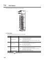
Part Names. . . . . . . . . . . . . . . . . . . . . . . . . . . . . . . . . . . . . . . . . . . . . . . . . . . . . . . . . . . . . . . 140
7.4
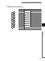
Wiring . . . . . . . . . . . . . . . . . . . . . . . . . . . . . . . . . . . . . . . . . . . . . . . . . . . . . . . . . . . . . . . . . . . 142
7.4.1
Wiring precautions . . . . . . . . . . . . . . . . . . . . . . . . . . . . . . . . . . . . . . . . . . . . . . . . . . . . . . . . 142
7.4.2
External wiring . . . . . . . . . . . . . . . . . . . . . . . . . . . . . . . . . . . . . . . . . . . . . . . . . . . . . . . . . . . 143
CHAPTER 8 VARIOUS SETTINGS
144
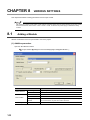
8.1
Adding a Module. . . . . . . . . . . . . . . . . . . . . . . . . . . . . . . . . . . . . . . . . . . . . . . . . . . . . . . . . . . 144
8.2
Switch Setting . . . . . . . . . . . . . . . . . . . . . . . . . . . . . . . . . . . . . . . . . . . . . . . . . . . . . . . . . . . . . 145
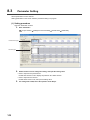
8.3
Parameter Setting. . . . . . . . . . . . . . . . . . . . . . . . . . . . . . . . . . . . . . . . . . . . . . . . . . . . . . . . . . 146
8.4
Auto Refresh. . . . . . . . . . . . . . . . . . . . . . . . . . . . . . . . . . . . . . . . . . . . . . . . . . . . . . . . . . . . . . 149
8.5
Offset/gain Setting . . . . . . . . . . . . . . . . . . . . . . . . . . . . . . . . . . . . . . . . . . . . . . . . . . . . . . . . . 150
8.5.1
Setting from "Offset/Gain Setting" of GX Works2. . . . . . . . . . . . . . . . . . . . . . . . . . . . . . . . . 150
8.5.2
Setting from a program . . . . . . . . . . . . . . . . . . . . . . . . . . . . . . . . . . . . . . . . . . . . . . . . . . . . 153
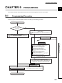
CHAPTER 9 PROGRAMMING
157
9.1
Programming Procedure. . . . . . . . . . . . . . . . . . . . . . . . . . . . . . . . . . . . . . . . . . . . . . . . . . . . . 157
9.2
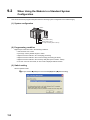
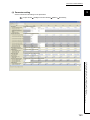
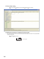
When Using the Module in a Standard System Configuration . . . . . . . . . . . . . . . . . . . . . . . . 158
9.3
9.2.1
Program example when using parameters of the intelligent function module . . . . . . . . . . . 160
9.2.2
Program example when not using parameters of the intelligent function module . . . . . . . . 164
When Using the Module on the Remote I/O Network. . . . . . . . . . . . . . . . . . . . . . . . . . . . . . . 167
9.3.1
Program example when using parameters of the intelligent function module . . . . . . . . . . . 175
9.3.2
Program example when not using parameters of the intelligent function module . . . . . . . . 177
CHAPTER 10 ONLINE MODULE CHANGE
182
10.1
Precautions on Online Module Change . . . . . . . . . . . . . . . . . . . . . . . . . . . . . . . . . . . . . . . . . 182
10.2
Conditions for Online Module Change . . . . . . . . . . . . . . . . . . . . . . . . . . . . . . . . . . . . . . . . . . 183
10.3
Online Module Change Operations . . . . . . . . . . . . . . . . . . . . . . . . . . . . . . . . . . . . . . . . . . . . 184
10.4
Online Module Change Procedure . . . . . . . . . . . . . . . . . . . . . . . . . . . . . . . . . . . . . . . . . . . . . 185
9
10.5
When a Factory Default Range Is Used and Parameters Are Set Using the Configuration
Function . . . . . . . . . . . . . . . . . . . . . . . . . . . . . . . . . . . . . . . . . . . . . . . . . . . . . . . . . . 187
10.6
When a Factory Default Range Is Used and Parameters Are Set Using a Sequence
Program . . . . . . . . . . . . . . . . . . . . . . . . . . . . . . . . . . . . . . . . . . . . . . . . . . . . . . . . . . 193
10.7
When a User Range Is Used and Parameters Are Set Using the Configuration Function
(with Another System) . . . . . . . . . . . . . . . . . . . . . . . . . . . . . . . . . . . . . . . . . . . . . . . . 200
10.8
When a User Range Is Used and Parameters Are Set Using a Sequence Program
(with Another System) . . . . . . . . . . . . . . . . . . . . . . . . . . . . . . . . . . . . . . . . . . . . . . . . 206
10.9
When a User Range Is Used and Parameters Are Set Using the Configuration Function
(without Another System) . . . . . . . . . . . . . . . . . . . . . . . . . . . . . . . . . . . . . . . . . . . . . . 213
10.10 When a User Range Is Used and Parameters Are Set Using a Sequence Program
(without Another System) . . . . . . . . . . . . . . . . . . . . . . . . . . . . . . . . . . . . . . . . . . . . . . 220
10.11 Range Reference Table . . . . . . . . . . . . . . . . . . . . . . . . . . . . . . . . . . . . . . . . . . . . . . . . . . . . . 227
CHAPTER 11 TROUBLESHOOTING
228
11.1
Error Code List . . . . . . . . . . . . . . . . . . . . . . . . . . . . . . . . . . . . . . . . . . . . . . . . . . . . . . . . . . . . 228
11.2
Alarm Code List . . . . . . . . . . . . . . . . . . . . . . . . . . . . . . . . . . . . . . . . . . . . . . . . . . . . . . . . . . . 235
11.3
11.4
Troubleshooting . . . . . . . . . . . . . . . . . . . . . . . . . . . . . . . . . . . . . . . . . . . . . . . . . . . . . . . . . . . 236
11.3.1
When the RUN LED flashes or turns off . . . . . . . . . . . . . . . . . . . . . . . . . . . . . . . . . . . . . . . 236
11.3.2
When the ERR. LED turns on or flashes . . . . . . . . . . . . . . . . . . . . . . . . . . . . . . . . . . . . . . . 236
11.3.3
When the ALM LED turns on or flashes. . . . . . . . . . . . . . . . . . . . . . . . . . . . . . . . . . . . . . . . 237
11.3.4
When a digital output value cannot be read. . . . . . . . . . . . . . . . . . . . . . . . . . . . . . . . . . . . . 237
11.3.5
When Conversion completed flag does not turn on in the normal mode . . . . . . . . . . . . . . . 238
Checking the CT Input Module Status on GX Works2 System Monitor . . . . . . . . . . . . . . . . . 239
APPENDICES
240
Appendix 1 Dedicated Instruction . . . . . . . . . . . . . . . . . . . . . . . . . . . . . . . . . . . . . . . . . . . . . . . . . . 240
Appendix 1.1
G(P).OFFGAN . . . . . . . . . . . . . . . . . . . . . . . . . . . . . . . . . . . . . . . . . . . . . 241
Appendix 1.2
G(P).OGLOAD . . . . . . . . . . . . . . . . . . . . . . . . . . . . . . . . . . . . . . . . . . . . 243
Appendix 1.3
G(P).OGSTOR . . . . . . . . . . . . . . . . . . . . . . . . . . . . . . . . . . . . . . . . . . . . 247
Appendix 2 When Using GX Developer . . . . . . . . . . . . . . . . . . . . . . . . . . . . . . . . . . . . . . . . . . . . . . 251
Appendix 2.1
Operation of GX Developer . . . . . . . . . . . . . . . . . . . . . . . . . . . . . . . . . . . . 251
Appendix 3 Online Module Change Procedure (When Using GX Developer) . . . . . . . . . . . . . . . . . 253
Appendix 3.1
Precautions on online module change . . . . . . . . . . . . . . . . . . . . . . . . . . . . . 253
Appendix 3.2
Conditions for online module change . . . . . . . . . . . . . . . . . . . . . . . . . . . . . . 254
Appendix 3.3
Online module change operations . . . . . . . . . . . . . . . . . . . . . . . . . . . . . . . . 255
Appendix 3.4
Online module change procedure . . . . . . . . . . . . . . . . . . . . . . . . . . . . . . . . 256
Appendix 3.5
When a factory default range is used and initial settings are configured
Appendix 3.6
When a user range is used and initial settings are configured using
using a sequence program . . . . . . . . . . . . . . . . . . . . . . . . . . . . . . . . . . . . . 257
a sequence program (with another system) . . . . . . . . . . . . . . . . . . . . . . . . . . 263
Appendix 3.7
When a user range is used and initial settings are configured using
a sequence program (without another system) . . . . . . . . . . . . . . . . . . . . . . . . 269
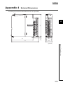
Appendix 4 External Dimensions . . . . . . . . . . . . . . . . . . . . . . . . . . . . . . . . . . . . . . . . . . . . . . . . . . . 275
10
INDEX
276
REVISIONS . . . . . . . . . . . . . . . . . . . . . . . . . . . . . . . . . . . . . . . . . . . . . . . . . . . . . . . . . . . . . . . . . . . . . . 278
WARRANTY . . . . . . . . . . . . . . . . . . . . . . . . . . . . . . . . . . . . . . . . . . . . . . . . . . . . . . . . . . . . . . . . . . . . . 279
11
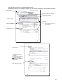
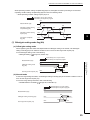
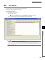
MANUAL PAGE ORGANIZATION
In this manual, pages are organized and the symbols are used as shown below.
The following illustration is for explanation purpose only, and should not be referred to as an actual documentation.
"" is used for window
names and items.
shows operating
procedures.
shows mouse
operations.*1
The chapter of
the current page is shown.
[ ] is used for items in
the menu bar and the
project window.
The section of
the current page is shown.
Ex. shows setting or
operating examples.
shows reference
manuals.
shows notes that
require attention.
shows reference
pages.
shows useful
information.
*1
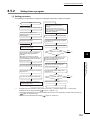
The mouse operation example is provided below.
Menu bar
Ex.
[Online]
[Write to PLC...]
Select [Online] on the menu bar,
and then select [Write to PLC...].
A window selected in the view selection area is displayed.
Ex.
[Parameter]
Project window
[PLC Parameter]
Select [Project] from the view selection
area to open the Project window.
In the Project window, expand [Parameter] and
select [PLC Parameter].
View selection area
12
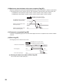
Pages describing instructions are organized as shown below.
The following illustration is for explanation purpose only, and should not be referred to as an actual documentation.
Instruction name
Execution condition of the instruction
Structure of the instruction
in the ladder mode
shows the devices
applicable to the instruction
Descriptions of
setting data and data type
Setting side
User : Device value is set by the user.
System: Device value is set by
the CPU module.
Descriptions of
control data (if any)
Detailed descriptions
of the instruction
Conditions for the error and
error codes
For the errors not described in
this manual, refer to the following.
QCPU User's Manual
(Hardware Design, Maintenance
and Inspection)
Simple program example(s)
and descriptions of the devices used
13
• Instructions can be executed under the following conditions.
Execution condition
Any time
Symbol
No symbol
On the rising
During on
edge
During off
On the falling
edge
• The following devices can be used.
Internal device
Setting
(system, user)
data
Applicable
device*1
Bit
Word
X, Y, M, L,
SM, F, B,
SB, FX,
FY
*2
T, ST, C, D,
W, SD,
SW, FD,
@
Link direct device
Intelligent
J\
function
File
register
Bit
R, ZR
Word
-
module device
U\G
U\G
Index
register
Zn
Z
*1
For details on each device, refer to the following.
*2
*3
Qn(H)/QnPH/QnPRHCPU User's Manual (Function Explanation, Program Fundamentals)
FX and FY can be used for bit data only, and FD for word data only.
In the "Constant" and "Others" columns, a device(s) that can be set for each instruction is shown.
QnUCPU User's Manual (Function Explanation, Program Fundamentals)
• The following data types can be used.
Data type
14
Description
Bit
Bit data or the start number of bit data
BIN 16-bit
16-bit binary data or the start number of word device
BIN 32-bit
32-bit binary data or the start number of double-word device
BCD 4-digit
Four-digit binary-coded decimal data
BCD 8-digit
Eight-digit binary-coded decimal data
Real number
Floating-point data
Character string
Character string data
Device name
Device name data
Constant
Others
*3
*3
K, H, E, $
P, I, J, U,
D, X, DY,
N, BL,
TR, BL\S,
V
TERM
Unless otherwise specified, this manual uses the following terms.
Term
Description
CT input module
The abbreviation for the Q68CT current transformer input module
CT
Another term for a current transformer
QCPU
Another term for the MELSEC-Q series CPU module
Process CPU
A generic term for the Q02PHCPU, Q06PHCPU, Q12PHCPU, and Q25PHCPU
Redundant CPU
A generic term for the Q12PRHCPU and Q25PRHCPU
GX Works2
Product name of the software package for the MELSEC programmable
GX Developer
controllers
Programming tool
Generic term for GX Works2 and GX Developer
An alternating current value measured using a CT. This manual describes a
CT input value
primary current value as a CT input value.
A generic term for factory-default input ranges (0 to 5AAC, 0 to 50AAC, 0 to
Factory default range
100AAC, 0 to 200AAC, 0 to 400AAC, and 0 to 600AAC)
A generic term for user-defined input ranges (0 to 5AAC, 0 to 50AAC, 0 to
User range
100AAC, 0 to 200AAC, 0 to 400AAC, and 0 to 600AAC)
The memory of an intelligent function module used to store data (such as setting
Buffer memory
values and monitored values) for communication with a CPU module.
PACKING LIST
The product package contains the following.
Model
Q68CT
-
Product
Quantity
Q68CT current transformer input module
1
Before Using the Product (BCN-P5901)
1
15
CHAPTER 1
OVERVIEW
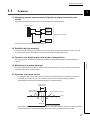
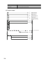
(1) CT
A CT means "Current Transformer" and is a current sensor which is necessary to measure an alternating current.
A CT is used for the following purposes widely.
• To control a load or monitor an operation of equipment and devices
• To control or monitor of an electric power system
When a high current is measured in an electric power receiving facility, measurement devices cannot be wired
directly. A CT is used for such a situation.
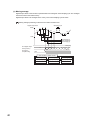
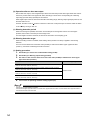
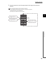
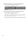
(a) Mechanism of a CT
A CT utilizes characteristics of an alternating current.
Iron core
Primary coil
Secondary coil
K
Primary current (I1)
k
Secondary current (I2)
Primary windings (T1)
L
Secondary windings (T2)
I
Primary and secondary coils winded an iron core are isolated
electrically. When a primary current (I1) is applied to the iron
core, a secondary current (I2) can be extracted depending on
the turn ratio (current transformation ratio).
The following shows the relationship of a primary current, a
secondary current, and windings
Primary current (I1)
(
Windings (T1) = Secondary current (I2)
Current transformation
ratio (CT ratio)
)
Windings (T2)
Primary current (I1)
Secondary windings (T2)
Secondary current (I2)
Primary windings (T1)
=
There are two CT types: the contact type and noncontact type. The noncontact type is classified into the
window-type and split-type which is easy to be retrofitted.
(2) Operation of a CT input module
A CT input module measures an alternating current by converting a secondary current input from a CT to a digital
value after carrying out an effective value operation.
The above flows are defined as "digital conversion" in this manual.
16
CHAPTER 1 OVERVIEW
1.1
Features
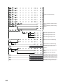
1
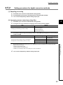
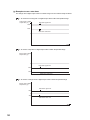
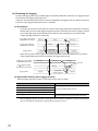
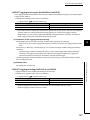
(1) Alternating current measurement of eight points (eight channels) by one
module
One module can measure an alternating current with eight points (eight channels).
CT input module
CT
CT
Measured
target 1
Measured
target 2
8 points (8 channels)
CT
Measured
target 8
A CT input range can be selected for each channel.
(2) Reliability by high accuracy
A CT input module can achieve the high accuracy of ±0.5% (when the ambient temperature is 25 ± 5°C) and
±1.0% (when the ambient temperature is 0 to 55°C) at the maximum digital output value.
(3) Operation of a digital output value by the scaling function
The scaling function can represent a digital output value in an easily understandable value depending on a
(4) Monitoring of a measured target
By using the input signal error detection function, warning output function, or dropout function, the status of a
measured target can be monitored easily.
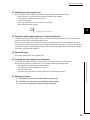
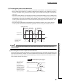
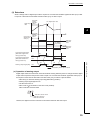
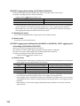
(5) Detection of the peak current
• By setting the peak current detection value and peak current detection time, the peak current occurred
excessively at a system start-up or an overload of devices can be detected. Doing so improves
maintainability of devices and the failure diagnosis for a measured target.
Peak current
detection time
Peak current
detection value
Current values from a CT
Time
Alarm ON
• The number of peak current detection is recorded in a non-volatile memory. Therefore the number of peak
current detection is not cleared after turning off the power supply or resetting the CPU module.
17
1.1 Features
purpose.
(6) Logging function
5000 data can be collected for each channel. The analysis of the collected data can improves maintainability of
the system used.
(7) Backup of a set value to a non-volatile memory
Initial settings in the buffer memory can be backed up to a non-volatile memory. Initial settings do not need to be
reset when the power supply is turned on or the CPU module is reset.
(8) Changeable slope of I/O conversion characteristics
A slope of I/O conversion characteristics can be changed by configuring the offset/gain settings.
(9) Easy setting with GX Works2
Sequence programming is reduced since initial settings or an auto refresh setting can be configured on the
screen. In addition, setting status and operating status of modules can be checked easily.
(10)Online module change
This module can be replaced without stopping the system.
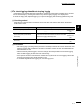
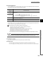
(11)Reduced man-hours and costs (A signal converter is not needed.)
A CT can be connected to a programmable controller directory using a CT input module; as a result, a signal
converter installed outside is not required. Therefore man-hours and costs are reduced.
Analog input module
DC voltage or
DC electricity
CT input module
Signal converters
are not required.
Signal converter
Secondary current
Secondary current
CT
CT
Primary current
Primary current
Measured target Measured target
<<Existing system>>
18
Measured target Measured target
<<System with a CT input module>>
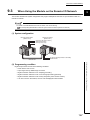
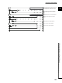
CHAPTER 2 SYSTEM CONFIGURATION
CHAPTER 2
SYSTEM CONFIGURATION
1
This chapter describes the system configuration of the CT input module.
2.1
2
Applicable Systems
This section describes applicable systems.
(1) Applicable CPU modules and base units, and number of mountable modules
(a) When mounted with a CPU module
The following table lists CPU modules and base units applicable to the CT input module and the number of
mountable CT input modules.
Depending on the combination with other modules or the number of mounted modules, power supply capacity
may be insufficient.
Select the power supply capacity according to the module to be used.
If the power supply capacity is insufficient, change the combination of the modules.
Applicable CPU module
CPU type
CPU model
Q00JCPU
Basic model QCPU
Q00CPU
modules*1
Applicable base unit*2
Main base unit
Extension base
unit
Up to 16
Up to 24
2.1 Applicable Systems
Q01CPU
Number of
Q02CPU
High Performance
model QCPU
Q02HCPU
Q06HCPU
Up to 64
Q12HCPU
Q25HCPU
Q02PHCPU
Process CPU
Q12PHCPU
Up to 64
Q25PHCPU
Programmable
controller CPU
Q06PHCPU
Redundant CPU
Q12PRHCPU
Q25PRHCPU
Q00UJCPU
Q00UCPU
Q01UCPU
Q02UCPU
Universal model
QCPU
Up to 53
×
Up to 16
Up to 24
Up to 36
Q03UDCPU
Q04UDHCPU
Q06UDHCPU
Q10UDHCPU
Up to 64
Q13UDHCPU
Q20UDHCPU
Q26UDHCPU
19
Applicable CPU module
CPU type
Applicable base unit*2
Number of
modules*1
CPU model
Extension base
Main base unit
unit
Q03UDECPU
Q04UDEHCPU
Q06UDEHCPU
Universal model
Programmable
QCPU
controller CPU
Q10UDEHCPU
Q13UDEHCPU
Up to 64
Q20UDEHCPU
Q26UDEHCPU
Q50UDEHCPU
Q100UDEHCPU
Safety CPU
QS001CPU
N/A
×*3
×
Q06CCPU-V
C Controller module
Q06CCPU-V-B
Up to 64
Q12DCCPU-V
: Applicable, ×: N/A
*1
*2
*3
Limited within the range of I/O points for the CPU module.
Can be mounted to any I/O slot of a base unit.
Connection of an extension base unit is not available with any safety CPU.
Remark
To use a C Controller module with the CT input module, refer to the C Controller Module User's Manual.
(b) When mounted on MELSECNET/H remote I/O station
The following table lists the network modules and base units applicable to the CT input module and the number
of mountable CT input modules.
Depending on the combination with other modules or the number of mounted modules, power supply capacity
may be insufficient.
Select the power supply capacity according to the module to be used.
If the power supply capacity is insufficient, change the combination of the modules.
Applicable network
module
Applicable base unit*2
Number of modules*1
Main base unit of remote
Extension base unit of
I/O station
remote I/O station
QJ72LP25-25
QJ72LP25G
QJ72LP25GE
Up to 64
QJ72BR15
: Applicable, ×: N/A
*1
*2
Limited within the range of I/O points for the network module.
Can be mounted to any I/O slot of a base unit.
Remark
The Basic model QCPU or C Controller module cannot configure the MELSECNET/ H remote I/O net.
20
CHAPTER 2 SYSTEM CONFIGURATION
1
(2) For multiple CPU system
The function version of the first released CT input module is C, and the CT input module supports multiple CPU
systems.
2
When using the CT input module in a multiple CPU system, refer to the following.
QCPU User's Manual (Multiple CPU System)
(a) Intelligent function module parameters
Write intelligent function module parameters to only the control CPU of the CT input module.
(3) For online module change
The CT input module supports online module change. For details on online module change, refer to the following.
ONLINE MODULE CHANGE (
Page 182, CHAPTER 10)
Online Module Change Procedure (When Using GX Developer) (
Page 253, Appendix 3)
2.1 Applicable Systems
21
(4) Applicable software packages
The following table lists systems that use a CT input module and applicable software packages.
A programming tool is required to use a CT input module.
Software version
Item
Q00J/Q00/Q01CPU
Q02/Q02H/Q06H/Q12H/Q25HCPU
Q02PH/Q06PHCPU
Q12PH/Q25PHCPU
Q12PRH/Q25PRHCPU
Q00UJ/Q00U/Q01UCPU
GX Developer*1
Single CPU system
Version 7 or later
Multiple CPU system
Version 8 or later
Single CPU system
Version 4 or later
Multiple CPU system
Version 6 or later
Single CPU system
Multiple CPU system
Single CPU system
Multiple CPU system
Redundant system
Single CPU system
Multiple CPU system
Q02U/Q03UD/Q04UDH/
Single CPU system
Q06UDHCPU
Multiple CPU system
Q10UDH/Q20UDHCPU
Q13UDH/Q26UDHCPU
Single CPU system
Multiple CPU system
Single CPU system
Multiple CPU system
Q03UDE/Q04UDEH/Q06UDEH/
Single CPU system
Q13UDEH/Q26UDEHCPU
Multiple CPU system
Q10UDEH/Q20UDEHCPU
Q50UDEH/Q100UDEHCPU
Single CPU system
Multiple CPU system
Single CPU system
Multiple CPU system
If installed in a MELSECNET/H remote I/O station
*1
22
GX Works2
Version 1.77F or later
Version 8.68W or later
N/A
Version 7.10L or later
Version 8.45X or later
Version 8.76E or later
Version 8.48A or later
Version 8.76E or later
Version 8.62Q or later
Version 1.77F or later
Version 8.68W or later
Version 8.76E or later
N/A
Version 6 or later
When using GX Developer, create a sequence program for initial settings and auto refresh setting.
CHAPTER 2 SYSTEM CONFIGURATION
1
(5) Products prepared by user
(a) CT
Manufacturer
Model name
CTF-5A
Input range
0 to 5AAC
3000 turns
CTF-50A
0 to 50AAC
3000 turns
Multi Measuring Instruments
CTF-100A
0 to 100AAC
3000 turns
Sales Co., Ltd.
CTF-200A
0 to 200AAC
3000 turns
CTF-400A
0 to 400AAC
6000 turns
CTF-600A
0 to 600AAC
9000 turns
CTL-10-3FC*1
0 to 5AAC, 0 to 50AAC
3000 turns
CTL-16-3FC*1
0 to 100AAC
3000 turns
CTL-24-3FC*1
0 to 200AAC
3000 turns
CTL-36-6SC*1
0 to 400AAC
6000 turns
CTT-36-9SC
0 to 600AAC
9000 turns
EMU-CT50
0 to 50AAC
3000 turns
EMU-CT100
0 to 100AAC
3000 turns
EMU-CT400
0 to 400AAC
6000 turns
EMU-CT600
0 to 600AAC
9000 turns
U.R.D.,LTD.
Mitsubishi Electric Corporation
*1
2
Secondary winding
The following connection cable is available for a connection with the CT input module.
Manufacturer
U.R.D.,LTD.
Model name
CABLE-4
Use a shielded twisted pair cable for a connection between the CT input module and CT. The shielded twisted
pair cable must satisfy the input specifications described in the performance specifications.
Performance Specifications (
Page 27, Section 3.2)
23
2.1 Applicable Systems
(b) Connection cable
2.2
How to Check the Function Version and Serial Number
The function version and serial number of a CT input module can be checked on the rating plate, front part of the
module, or system monitor of the programming tool.
(1) Checking on the rating plate
The rating plate is on the side of the CT input module.
Serial number (first five digits)
Function version
Relevant regulation standards
(2) Checking on the front part (bottom part) of module
The function version and serial number on the rating plate are also shown on the front part (bottom part) of the
module.
Function version
14011000000000-C
Serial number
24
CHAPTER 2 SYSTEM CONFIGURATION
1
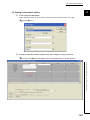
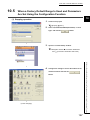
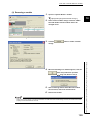
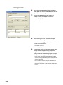
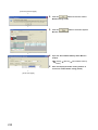
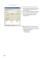
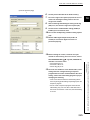
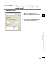
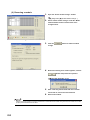
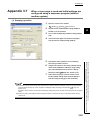
(3) Checking on the system monitor
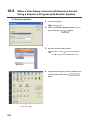
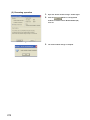
The function version and serial number can be checked on the "Product Information List" window.
[Diagnostics]
2
[System Monitor...]
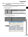
(a) Displaying product number
For the CT input module, "-" is displayed since the product number display is not supported.
● The serial number on the rating plate and front part of the module indicates the management information of the product.
● The serial number displayed on the product information list of a programming tool indicates the function information of the
product. The function information of the product is updated when a new function is added.
25
2.2 How to Check the Function Version and Serial Number
The serial number displayed on the product information list of a programming tool may differ from that on the rating plate and
on the front part of the module.
CHAPTER 3
SPECIFICATIONS
This chapter describes general specifications, performance specifications, I/O conversion characteristics, accuracy,
and functions.
3.1
General Specifications
For the general specifications of the CT input module, refer to the following.
QCPU User's Manual (Hardware Design, Maintenance and Inspection)
26
CHAPTER 3 SPECIFICATIONS
3.2
Performance Specifications
1
This section describes the performance specifications of the CT input module.
3.2.1
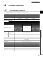
Performance specifications list
3
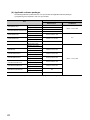
The following table lists the performance specifications of the CT input module.
Item
Specifications
Number of input points
8 points (8 channels)
Operation method
Effective value operation
Input range
0 to 5AAC
0 to 50AAC
0 to 100AAC
0 to 200AAC
0 to 400AAC
0 to 600AAC
Converted
Digital output
0 to 12000
current value
Scaling value
-32768 to 32767
Input frequency
50/60Hz
Excessive input
200% for 1 minute, 150% for continuous time
Input range
I/O characteristics, maximum
resolution
Digital output value
Maximum resolution
0 to 5AAC
0.5mA
0 to 50AAC
5mA
0 to 100AAC
10mA
0 to 10000
0 to 200AAC
20mA
40mA
0 to 600AAC
60mA
3.2 Performance Specifications
3.2.1 Performance specifications list
0 to 400AAC
Ambient
Accuracy
temperature
(accuracy for the
25 ± 5°C
maximum digital
Ambient
output value)*1*2
temperature
Within ± 0.5% (±50 digits)
Within ± 1.0% (±100 digits)
0 to 55°C
Sampling cycle*3
Response time*4
Number of access to the non-volatile
memory
Isolation method
10ms/8CH
20ms/8CH
50ms/8CH
100ms/8CH
0.4s or less
Up to 1012 times
Between input terminals and the programmable controller power supply: Transformer
Between input channels: No isolation
Dielectric withstand voltage
Between I/O terminals and the programmable controller power supply: 1500VACrms for 1 minute
Insulation resistance
Between I/O terminals and the programmable controller power supply: 500VDC 10MΩ or higher
Number of occupied I/O points
External connection system
Applicable wire size
Applicable solderless terminal
16 points (I/O assignment: 16 points for intelligent)
18-point terminal block
0.3 to 0.75mm2
R1.25-3 (Do not use a solderless terminal with an insulation sleeve.)
Internal current consumption (5VDC)
0.35A
Weight
0.19kg
27
*1
*2
*3
*4
Except in case when the CT input module is influenced by noise
The accuracy when a CT is connected is a sum of the CT input module's accuracy and the CT's accuracy.
The following is the formula to calculate accuracy.
(Accuracy) = (Accuracy of the CT input module) + (Accuracy of the CT to be used)
For the accuracy of the CT to be used, contact its manufacturer.
The default value is 10ms/8CH.
Response time complies with IEC 60688.
The larger one of the following
• The time from when the CT input changes from 0 to 90% till when the converted digital value reaches 90% ± 1%
• The time from when the CT input changes from 100 to 10% till when the converted digital value reaches 10% ± 1%
28
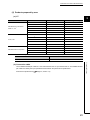
CHAPTER 3 SPECIFICATIONS
3.2.2
I/O conversion characteristics
1
An I/O conversion characteristic is expressed with the slope of the line connecting an offset value and gain value when
a CT input value (current) is converted to a digital value.
(1) Offset value
3
This is the CT input value (current) converted to the digital output value of 0.
(2) Gain value
This is the CT input value (current) converted to the digital output value of 10000.
(3) I/O conversion characteristics
The following graph shows the I/O conversion characteristics.
Practical input range
12000
1)
10000
2)
3)
5)
4)
3.2 Performance Specifications
3.2.2 I/O conversion characteristics
Digital
output
value
6)
0
50
100
200
400
600
CT input value (A)
Digital output value*1
Maximum
No.
Input range setting
Offset value
Gain value
1)
0 to 5AAC
0A
5A
0.5mA
2)
0 to 50AAC
0A
50A
5mA
3)
0 to 100AAC
0A
100A
4)
0 to 200AAC
0A
200A
5)
0 to 400AAC
0A
400A
40mA
6)
0 to 600AAC
0A
600A
60mA
*1
0 to 10000
resolution
10mA
20mA
If an analog value is input exceeding the digital output range, the digital output value is fixed to the maximum (12000) or
minimum (0).
29
● Use the CT input module so that the input and output are within the specified practical ranges. If a value is out of the
range, the maximum resolution and accuracy may not fall within the range described in performance specifications.
(Avoid values on the dotted line region in the graph of I/O conversion characteristics.)
● For each input range, avoid inputting a value that exceeds the one in the following table to the CT. (Avoid inputting the
value that is 150% or more over the maximum input range.) Elements may be damaged.
30
Input range setting
CT input value (primary current value of a CT)
0 to 5AAC
7.5A or more
0 to 50AAC
75A or more
0 to 100AAC
150A or more
0 to 200AAC
300A or more
0 to 400AAC
600A or more
0 to 600AAC
900A or more
CHAPTER 3 SPECIFICATIONS
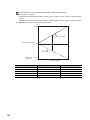
3.2.3
Accuracy
1
The accuracy of the CT input module is measured for the maximum digital output value.
Even if the offset/gain setting or input range was changed to change input characteristics, the accuracy remains the
same, and is kept within the range described in performance specifications.
The following graph shows the fluctuation range of accuracy when the range of 0 to 200AAC is selected.
3
The accuracy is ±0.5% (±50 digits) when the ambient temperature is 25 ± 5°C, and ±1.0% (±100 digits) when the
ambient temperature is 0 to 55°C (excluding the case under noise effect).
10000
Fluctuation
range
Digital
output
value
3.2 Performance Specifications
3.2.3 Accuracy
0
0
200
CT input value (A)
31
3.2.4
Number of parameter settings
Set initial settings and auto refresh settings of the CT input module so that the number of parameters, including those
of other intelligent function modules, does not exceed the number of parameters that can be set in the CPU module.
For the maximum number of parameters that can be set in the CPU module, refer to the following.
QCPU User's Manual (Hardware Design, Maintenance and Inspection)
(1) Number of CT input module parameters
For a CT input module, the following number of parameters can be set.
Model
Initial setting
Auto refresh setting
Q68CT
14
89 (maximum)
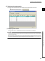
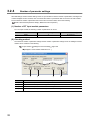
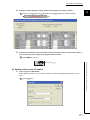
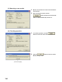
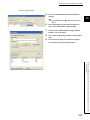
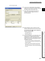
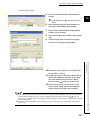
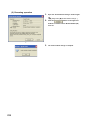
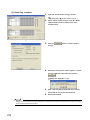
(2) Checking method
The maximum number of parameter settings and the number of parameter settings set for the intelligent function
module can be checked on the following.
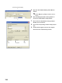
Project window
[Intelligent Function Module]
Right-click
[Intelligent Function Module Parameter List...]
1)
No.
32
2)
3)
4)
Description
1)
The total number of parameters in initial settings checked on the window
2)
The maximum number of parameter settings in initial settings
3)
The total number of parameters in the auto refresh setting checked on the window
4)
The maximum number of parameter settings in the auto refresh setting
CHAPTER 3 SPECIFICATIONS
3.3
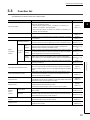
Function list
1
The following is the function list of the CT input module.
Item
Description
Reference
An input range can be selected for each channel depending on a measured
3
target from the following ranges.
• Factory default ranges (0 to 5AAC, 0 to 50AAC, 0 to 100AAC, 0 to
Input range setting
200AAC, 0 to 400AAC, and 0 to 600AAC)
Page 36,
Section 4.2
• User ranges (0 to 5AAC, 0 to 50AAC, 0 to 100AAC, 0 to 200AAC, 0 to
400AAC, and 0 to 600AAC)
Conversion enable/disable function
Sampling cycle switching function
Sampling processing
Time
average
Digital
conversion
method
Averaging
Count
process
average
Digital conversion can be enabled or disabled for each channel.
A sampling cycle can be selected from 10ms/8CH, 20ms/8CH, 50ms/8CH,
or 100ms/8CH.
Page 37,
Section 4.4
CT input values are converted to digital values in each sampling cycle. The
Page 38,
converted values are stored as digital output values in the buffer memory.
Section 4.5.1 (1)
Digital conversion is performed for a set time, and a sum of the converted
values except the maximum and minimum values is averaged. The
averaged values are stored in the buffer memory.
Page 39,
Section 4.5.1 (2)
(a)
Digital conversion is performed the set number of times, and a sum of the
Page 39,
converted values except the maximum and minimum values is averaged.
Section 4.5.1 (2)
The averaged values are stored in the buffer memory.
Moving
Digital output values for the specified number of times are averaged in
average
each sampling cycle. The averaged values are stored in the buffer memory.
Depending on the set time constant, digital output values with smoothed
noise can be obtained.
(b)
Page 40,
Section 4.5.1 (2)
(c)
Page 41,
Section 4.5.1 (3)
Overrange of a CT input value (excess of a peak value) can be detected.
Input signal error detection function
Since a CT input module can detect that a high current out of range flew
Page 44,
through a measured target, an error on the measured target is monitored
Section 4.6
easily.
When digital output values exceed the set peak current detection value
Peak current detection function
consecutively for the duration of the peak current detection time set in
advance, an error can be detected.
When an input current is around 0A, a CT's conversion accuracy is low. To
Dropout function
avoid digital output of such an unstable CT input value, digital output values
within the set value can be dropped to 0 forcibly.
A digital output value can be scaled into a value within the range of the set
Scaling function
scaling upper limit value to lower limit value.
The sequence programming for scale conversion can be omitted.
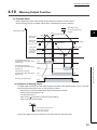
Warning
Process alarm
output
function
When a digital output value enters the alert output range set in advance, an
alert is output.
When a change rate of a digital output value is equal to or more than the
Rate alarm
rate alarm upper limit value (%/s) or that is equal to or less than the rate
alarm lower limit value (%/s), an alert is output.
Maximum value/minimum value hold
The maximum and minimum of digital output values or scaling values are
function
stored to the buffer memory for each channel.
Logging function
A digital output value or scaling value can be logged. 5000 data can be
logged for each channel.
Page 46,
Section 4.7
Page 49,
Section 4.8
Page 50,
Section 4.9
Page 53,
Section 4.10 (1)
Page 55,
Section 4.10 (2)
Page 59,
Section 4.11
Page 60,
Section 4.12
33
3.3 Function list
Primary delay filter
Page 37,
Section 4.3
Item
Description
Reference
Set values in the buffer memory can be backed up into the non-volatile
Set value backup function
memory. Since backup data are restored at the next start-up, programs for
initial settings are not required after the set value backup function was
Page 72,
Section 4.13
executed.
Default setting registration function
Values in the buffer memory can be changed back to the default.
Offset/gain setting
A slope of I/O conversion characteristics can be changed.
Error history function
Module error collection function
Errors and alarms occurred in the CT input module are stored up to the
latest 16 records in the buffer memory.
Errors and alarms occurred in the CT input module can be collected into
the CPU module.
Error clear function
When an error occurs, the error can be cleared on the system monitor.
Online module change
A module can be replaced without stopping the system.
34
Page 73,
Section 4.14
Page 150,
Section 8.5
Page 74,
Section 4.15
Page 77,
Section 4.16
Page 78,
Section 4.17
Page 182,
CHAPTER 10
CHAPTER 4 FUNCTIONS
CHAPTER 4
FUNCTIONS
1
This chapter describes the details of the CT input module's function, and the setting procedures for the functions.
For details on I/O signals and the buffer memory, refer to the following.
• Details of I/O Signals (
Page 80, Section 5.2)
• Details of Buffer Memory Addresses (
4.1
Page 106, Section 6.2)
Processing Each Function
4
A CT input value and digital value are processed in the following order. If multiple functions are enabled, the output of
the first-processed function is used as the input for the next function.
CT input
value
(CH1 to CH8)
Input signal
error detection
function
Peak current
detection
function
Dropout
function
Averaging
process
Warning
output
function
Scaling function
Digital output
value
Minimum value
Scaling value
Maximum value
Logging
function
Logging data
4.1 Processing Each Function
(1) CT input value
This is an alternating current value measured using a CT. This is a primary current which a CT imports.
(2) Digital output value
A digital value after the sampling processing or an averaging process was performed.
(3) Scaling value
This is a digital output value which was performed scale conversion.
(4) Maximum and minimum values
Either of the following are stored.
• The maximum and minimum digital output values (when the scaling function is disabled.)
• The maximum and minimum scaling values (when the scaling function is enabled.)
(5) Logging data
A digital output value or scaling value is collected.
35
4.2
Input Range Setting
An input range can be selected for each channel depending on the CT to be connected.
Select a factory default range normally. If the slope of I/O conversion characteristics is changed, select a user range
and configure the offset/gain setting.
● Select an input range depending on the CT to be connected. In case of excessive input, safety problems such as heat
generation may occur.
● If a set input value is not supported by the CT to be connected, and Operating condition setting request (Y9) is turned on
then off, an input signal error may occur.
If an input signal error occurs, check if the input range setting is supported by the connected CT. If the input range setting
is incorrect, reset the setting.
For details on the input signal error detection function, refer to the following.
• Input Signal Error Detection Function (
Page 44, Section 4.6)
(1) Setting procedure
1.
Set values to CH Input range setting (Un\G150 to Un\G157) depending on the CT to be
connected.
Input range
Factory default range
User range
2.
Setting value
0 to 5AAC
0000H
0 to 50AAC
0001H
0 to 100AAC
0002H
0 to 200AAC
0003H
0 to 400AAC
0004H
0 to 600AAC
0005H
0 to 5AAC
0010H
0 to 50AAC
0011H
0 to 100AAC
0012H
0 to 200AAC
0013H
0 to 400AAC
0014H
0 to 600AAC
0015H
Turn on then off Operating condition setting request (Y9).
(2) When using a user range
• Set 0010H to 0015H to CH Input range setting (Un\G150 to Un\G157) depending on the CT to be
connected.
• Configure the offset/gain setting. For the offset/gain setting, refer to
Page 150, Section 8.5.
• One offset value and one gain value are saved in the CT input value as the user range setting for each
channel. When connecting a new CT to a channel where a user range was set with a different CT before,
configure the offset/gain setting again.
36
CHAPTER 4 FUNCTIONS
4.3
Conversion Enable/Disable Function
1
Set whether to enable or disable the digital conversion for each channel.
(1) Setting procedure
1.
2.
4.4
Set Enable (0) or Disable (1) to Conversion enable/disable setting (Un\G0).
Turn on then off Operating condition setting request (Y9).
4
Sampling Cycle Switching Function
A sampling cycle can be selected from one of the following.
• 10ms/8CH
• 20ms/8CH
• 50ms/8CH
• 100ms/8CH
(1) Setting procedure
1.
Set a sampling cycle to Sampling cycle setting (Un\G26).
Item
Setting
• 10ms/8CH (0)
Sampling cycle setting (Un\G26)
• 20ms/8CH (1)
• 50ms/8CH (2)
2.
4.3 Conversion Enable/Disable Function
• 100ms/8CH (3)
Turn on then off Operating condition setting request (Y9).
Digital conversion is performed in the set sampling cycle regardless of the number of conversion enabled channels.
37
4.5
Digital Conversion Method
One of the following digital conversion methods can be set for each channel.
• Sampling processing
• Averaging process
• Primary delay filter
For the operation of each digital conversion method, refer to the following.
• Operations of digital conversion methods (
Page 38, Section 4.5.1)
For the setting procedure for each digital conversion method, refer to the following.
• Setting procedures for digital conversion methods (
4.5.1
Page 43, Section 4.5.2)
Operations of digital conversion methods
(1) Sampling processing
CT input values are converted to digital values in each set sampling cycle. The converted values are stored as
digital output values in the buffer memory.
(2) Averaging process
Digital output values are averaged for each channel. The averaged values are stored as digital output values in
the buffer memory.
There are three types of averaging process as follows:
• Time average
• Count average
• Moving average
38
CHAPTER 4 FUNCTIONS
(a) Time average
Digital conversion is performed for the duration of the set time, and a sum of the converted values except the
1
maximum and minimum values is averaged. The averaged value is stored in the buffer memory.
The number of processing within the duration of the set time varies depending on the set time and sampling
cycle.
Number of
processing
=
Set time
Sampling cycle
Ex. The number of processing is as follows in case of the settings below.
Item
Setting
Sampling cycle
50ms/8CH
Set time
380ms
380
50
= 7.6 (times)
4
Figures after the decimal point are omit.
Conversion is processed seven times to output the average value.
The valid lower limit setting value for a time average is calculated as: "(Minimum 4 times) × (Sampling cycle)".
Ex. When the sampling cycle is 50ms/8CH:
4 × 50 = 200ms
If the number of processing is less than four due to the set time, the error (error code: 20) occurs and the digital output
value becomes 0.
4.5 Digital Conversion Method
4.5.1 Operations of digital conversion methods
(b) Count average
Digital conversion is performed the set number of times, and a sum of the converted values except the
maximum and minimum values is averaged. The averaged value is stored in the buffer memory.
The processing time that takes to store the averaged value of count average in the buffer memory varies
depending on the sampling cycle.
Processing time = Set number of times
Sampling cycle
Ex. The processing time is as follows in case of the settings below.
Item
Setting
Sampling cycle
50ms/8CH
Set number of times
20 times
20 × 50 = 1000 (ms) → The averaged value is output in each 1000ms.
Since the count average requires a sum of at least two digital conversions besides the maximum and minimum values, the
set number of times must be four or more.
39
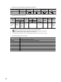
(c) Moving average
Digital output values of the number of specified times are averaged in each sampling cycle. The averaged
values are stored in the buffer memory.
Digital output values to be averaged move one by one in each sampling cycle as below.
Ex. Moving average processing of when the set number of times is four
Sampling cycle
Digital output value
10000
2)
3)
4)
5)
1)
6)
7)
8)
9)
12)
10) 11)
5000
1st storage (a)
2nd storage (b)
3rd storage (c)
0
Time [ms]
CH1 Digital output
value (Un\G11)
Conversion
completed flag
0
(a)
(b)
(c)
ON
OFF
Data transition in buffer memory
40
1st storage (a)
2nd storage (b)
3rd storage (c)
1) + 2) + 3) + 4)
2) + 3) + 4) + 5)
3) + 4) + 5) + 6)
4
4
4
CHAPTER 4 FUNCTIONS
1
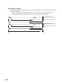
(3) Primary delay filter
Depending on the set time constant, digital output values with smoothed noise can be obtained. A smoothing
degree varies by setting the time constant.
The following are the relational expressions of time constants and digital output values.
[n = 1]*1
Yn = 0
[n = 2]
Yn = yn-1 +
t
t + TA
4
(yn - yn-1)
[n ≥ 3]
Yn = Yn-1 +
*1
*2
t
t + TA
(yn - Yn-1)
Yn
: Present digital output value
yn
: Digital output value before smoothing
Yn-1
: Last digital output value
yn-1
: Last digital output value before smoothing
n
:
Δt
: Sampling cycle
TA
: Time constant*2 (ms)
Number of sampling
processing
When n is 2 or larger, Conversion completed (1) is stored in Conversion completed flag (Un\G10).
Set a value which is equal to or larger than the sampling cycle. If the time constant is smaller than the sampling cycle,
the error (error code: 32) occurs, and the digital output value becomes 0.
4.5 Digital Conversion Method
4.5.1 Operations of digital conversion methods
41
Ex. 1: Change of digital output values under the following conditions
• Input range: 0 to 100AAC
• Sampling cycle: 10ms/8CH
• Time constant setting: 1000ms (1s)
• CT input value: changed from 0A to 100A
When 1000ms passes after the CT input value reaches 100A, the digital output value with a primary delay filter
reaches 63.2% of the digital output value in the sampling process.
CT input value
Digital output value
120
12000
100
10000
8000
80
63.2%
CT input value (A) 60
6000 Digital output value
40
4000
20
2000
0
0
0
1000
Time (ms)
Ex. 2: When CT input values form a ringing waveform, change of digital output values in the following
conditions
• Time constant setting: 2000ms (2s)
• Time constant setting: 1000ms (1s)
• Moving average processing: 16 times
CT input value
Digital output value (Moving
average processing:16 times)
Digital output value (Time constant setting: 1000ms)
Digital output value (Time constant setting: 2000ms)
120
12000
100
10000
80
8000
60
6000
40
4000
20
2000
CT input value (A)
Digital output value
0
42
0
0
Time (ms)
CHAPTER 4 FUNCTIONS
4.5.2
Setting procedures for digital conversion methods
1
(1) Sampling processing
1.
2.
3.
Set Enable (0) to Conversion enable/disable setting (Un\G0).
Set Sampling processing (0) to Averaging process setting (Un\G24, Un\G25).
Turn on then off Operating condition setting request (Y9).
(2) Averaging process and primary delay filter
1.
2.
4
Set Enable (0) to Conversion enable/disable setting (Un\G0).
Set digital conversion methods to Averaging process setting (Un\G24, Un\G25).
Item
Setting
• Time average (1)
Averaging process setting (Un\G24, Un\G25)
• Count average (2)
• Moving average (3)
• Primary delay filter (4)
3.
Set values to CH Average time/Average number of times/Moving average/Time constant settings
(Un\G1 to Un\G8)
Item
Processing
Setting range
Time average
40 to 5000 (ms)*1
CH Average time/Average number of times/Moving
Count average
4 to 500 (times)
average/Time constant settings (Un\G1 to Un\G8)
Moving average
2 to 1000 (times)
Primary delay filter
10 to 10000 (ms)*1
4.
4.5 Digital Conversion Method
4.5.2 Setting procedures for digital conversion methods
*1
Set an integral multiple of the sampling cycle. If not, digital output values are averaged in the maximum cycle that
satisfies both of the following.
• Duration of the set time or less
• Integral multiple of the sampling cycle
In addition, set a value per 10ms unit. A value per 1ms unit is rounded off.
Turn on then off Operating condition setting request (Y9).
43
4.6
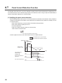
Input Signal Error Detection Function
Overrange of a CT input value (excess of a peak value) can be detected. Since a CT input module can detect that a
high current out of range flew through a measured target, an error on the measured target is monitored easily.
Controlled by the CT input module
Controlled by the sequence program
Alternating
current waveform
Overrange
occurrence
Peak value
Returns to
the measurement
range
Current value from the CT
Measurement range
of an input range
0
Time
Peak value
CH1 Input signal error detection flag
(Un\G49.b0)
ON
Sampling cycle
OFF
OFF
ON
Input signal error detection signal (XC)
OFF
ON
OFF
ON
CH1 Conversion completed
flag (Un\G10.b0)
CH1 Digital output value (Un\G11)
OFF
Value returned to
the measurement range
Value before the
overrange occurrence
ON
Error clear request (YF)
OFF
Latest error code (Un\G19)
OFF
0
0
Error occurrence
(1) Detection level of Input signal errors
The level of current that is detected as an input signal error depends on the input range setting. The current level
is about 125% of the gain value for the input range.
Input range setting
Factory default range 0 to 5AAC
User range 0 to 5AAC
Factory default range 0 to 50AAC
User range 0 to 50AAC
Factory default range 0 to 100AAC
User range 0 to 100AAC
Factory default range 0 to 200AAC
User range 0 to 200AAC
Factory default range 0 to 400AAC
User range 0 to 400AAC
Factory default range 0 to 600AAC
User range 0 to 600AAC
44
Detection level
Approximately 6.25AAC
Approximately 62.5AAC
Approximately 125AAC
Approximately 250AAC
Approximately 500AAC
Approximately 750AAC
CHAPTER 4 FUNCTIONS
1
(2) Notifying an input signal error
When a CT input value exceeds the input range, an input signal error is notified as follows.
• Input signal error (1) is stored in Input signal error detection flag (Un\G49).
• Input signal error detection signal (XC) turns on.
• The ALM LED flashes.
• Alarm code 110 is stored in Latest error code (Un\G19).
Alarm codes are stored as below.
110
Fixed
4
Input signal error channel number
(3) Operation of the input signal error detection function
In addition, Converting or unused (0) is stored in Conversion completed flag (Un\G10) on the corresponding
channel, and Conversion completed flag (XE) turns off.
When the CT input value returns within the input range, the digital conversion resumes regardless of reset of
Input signal error detection flag (Un\G49) and Input signal error detection signal (XC). Conversion completed (1)
is stored in Conversion completed flag (Un\G10) on the corresponding channel after the first update of a digital
output value. (The ALM LED is flashing.)
(4) Detection cycle
This function is executed in each sampling cycle.
(5) Clearing the input signal error detection
4.6 Input Signal Error Detection Function
After the CT input value returns within the input range, turn on then off Error clear request (YF).
When the input signal error is cleared, the CT input module results in the following states:
• Input signal error detection flag (Un\G49) is cleared.
• Input signal error detection signal (XC) turns off.
• The ALM LED turns off.
• The alarm code 110 which is stored in Latest error code (Un\G19) is cleared.
(6) Setting procedure
1.
2.
3.
Set Enable (0) to Conversion enable/disable setting (Un\G0).
Set Enable (0) to Input signal error detection setting (Un\G47).
Turn on then off Operating condition setting request (Y9).
45
4.7
Peak Current Detection Function
An abnormal current value from a CT can be detected. The peak current occurred excessively at a system start-up or
an overload of devices can be detected using the peak current detection function. Doing so improves maintainability of
devices and the failure diagnosis for a measured target.
(1) Notifying the peak current detection
When CH Digital output value (Un\G11 to Un\G18) exceeds set CH Peak current detection value (Un\G326 to
Un\G333) consecutively for the duration of set CH Peak current detection time (Un\G318 to Un\G325), an error
is notified as follows.
• Peak current detected (1) is stored in Peak current detection flag (Un\G301).
• Peak current detection signal (X7) turns on.
• The ALM LED flashes.
• Alarm code 120 is stored in Latest error code (Un\G19).
Alarm codes are stored as below.
120
Fixed
Peak current detection channel number
However, digital conversion on the channel where an error is notified was held.
Controlled by the CT input module
Controlled by the sequence program
Digital output value
Peak current
detection time
Peak current
detection value
Time
ON
CH1 Peak current
detection flag
(Un\G301.b0)
OFF
Peak current detection
signal (X7)
OFF
OFF
ON
OFF
ON
Error clear request (YF)
46
OFF
OFF
CHAPTER 4 FUNCTIONS
1
(2) Counting the peak current detection
• The number of peak current detection is stored in CH Peak current detection count (Un\G334 to Un\G341).
• When a peak current is detected, 1 is added in CH Peak current detection count (Un\G334 to Un\G341).
However, next addition is not performed unless a digital output value falls below the peak current detection
value once.
• CH Peak current detection count (Un\G334 to Un\G341) is saved automatically in the non-volatile memory
in the CT input module. When the module starts up by turning off then on, or resetting the CPU module, the
saved detection count is read in CH Peak current detection count (Un\G334 to Un\G341). Therefore, the
number of peak current detection is not cleared even after the power supply was turned off then on, or the
CPU module was reset.
4
• The count range of CH Peak current detection count (Un\G334 to Un\G341) is 0 to 32767. When the
number of peak current detection exceeds the upper limit of the count range, the number returns to 0.
Digital output value
Peak current Peak current
detection time detection time
Peak current
detection time
Peak current
detection value
Time
CH1 Peak current
detection count
(Un\G334)
0
1
32767
0
(a) Resetting the number of peak current detection
To reset the number of peak current detection, store Reset requested (1) in CH Peak current detection count
reset request (Un\G302 to Un\G309). 0 is stored in CH Peak current detection count (Un\G334 to Un\G341).
After the reset was completed, Reset request completed (1) is stored in CH Peak current detection count
reset complete (Un\G310 to Un\G317).
Controlled by the CT input module
Controlled by the sequence program
CH1 Peak current
detection count
(Un\G334)
CH1 Peak current
detection count reset
complete (Un\G310)
CH1 Peak current
detection count reset
request (Un\G302)
Detection count before reset
0
ON
OFF
OFF
ON
OFF
OFF
47
4.7 Peak Current Detection Function
When a digital output value has exceeded the peak current detection value at power on, the number of peak current
detection is added 1.
(3) Peak current detection time
The setting range of CH Peak current detection time (Un\G318 to Un\G325) is 10 to 10000ms.
Set CH Peak current detection time (Un\G318 to Un\G325) to an integral multiple of the sampling cycle.
When CH Peak current detection time (Un\G318 to Un\G325) is not set as the integral multiple of the sampling
cycle, the peak current is detected in the maximum cycle that satisfy both of the following.
• Peak current detection time or less
• Integral multiple of the sampling cycle
Ex. When the sampling cycle setting and peak current detection time is set to 100ms/8CH and 950ms, the
peak current is detected in 900ms intervals (integral multiple of 100ms).
(4) Clearing the notification of the peak current detection
Check that a digital output value is the peak current detection value or less, and turn on then off Error clear
request (YF).
When the notification of the peak current detection is cleared, the CT input module results in the following states:
• Peak current detection flag (Un\G301) is cleared.
• Peak current detection signal (X7) turns off.
• The ALM LED turns off.
• The alarm code 120 which is stored in Latest error code (Un\G19) is cleared.
When Error clear request (YF) is turned on then off in the condition where a digital output value exceeds the peak current
detection value, the peak current detection is notified again after a lapse of the peak current detection time.
(5) Detection target
CH Digital output value (Un\G11 to Un\G18) is a target regardless of the use of the scaling function.
(6) Setting procedure
1.
2.
3.
Set Enable (0) to Conversion enable/disable setting (Un\G0).
Set Enable (0) to Peak current detection setting (Un\G300).
Set values to CH Peak current detection time (Un\G318 to Un\G325) and CH Peak current
detection value (Un\G326 to Un\G333).
Item
CH Peak current detection time (Un\G318 to Un\G325)
10 to 10000 (ms)*1
CH Peak current detection value (Un\G326 to Un\G333)
0 to 11999
*1
4.
48
Setting range
Set an integral multiple of the sampling cycle. If not, the peak current is detected in the maximum cycle that satisfies
both of the following.
• Peak current detection time or less
• Integral multiple of the sampling cycle
In addition, set a value per 10ms unit. A value per 1ms unit is rounded off.
Turn on then off Operating condition setting request (Y9).
CHAPTER 4 FUNCTIONS
4.8
Dropout Function
1
When an input current is around 0A, a CT's conversion accuracy is low. To avoid digital output of such an unstable CT
input value, digital output values within the set value can be dropped to 0 forcibly.
(1) Operation of the dropout function
When the value in CH Digital output value (Un\G11 to Un\G18) is equal to or less than the set value in CH
Dropout value (Un\G162 to Un\G169) in advance, 0 is stored in CH Digital output value (Un\G11 to Un\G18).
4
(2) Setting procedure
1.
2.
3.
Set Enable (0) to Conversion enable/disable setting (Un\G0).
Set Enable (0) to Dropout detection setting (Un\G160).
Set values to CH Dropout value (Un\G162 to Un\G169).
Item
Setting range
CH Dropout value (Un\G162 to Un\G169)
4.
1 to 10000
Turn on then off Operating condition setting request (Y9).
Remark
To check whether the dropout function is enabled or disabled, refer to the following.
• Dropout status flag (Un\G161) (
Page 121, Section 6.2 (23))
4.8 Dropout Function
49
4.9
Scaling Function
A digital output value can be scaled into a value within the range of the set scaling upper limit value to lower limit value.
The sequence programming for scale conversion can be omitted.
The scale-converted values are stored in CH Scaling value (Un\G54 to Un\G61).
(1) Concept of scaling setting
Set values corresponding to the lower limit value (0) of the input range to CH Scaling lower limit value (Un\G62,
Un\G64, Un\G66, Un\G68, Un\G70, Un\G72, Un\G74, Un\G76).
Set values corresponding to the upper limit value (10000) of the input range to CH Scaling upper limit value
(Un\G63, Un\G65, Un\G67, Un\G69, Un\G71, Un\G73, Un\G75, Un\G77).
(2) Calculation method for a scaling value
A value is performed scale conversion using the following formula. The scaled values after the decimal point are
rounded off.
Scaling value =
DX
(SH - SL)
+ SL
DMax
Item
Description
Dx
Digital output value
DMax
Maximum digital output value for the used input range (10000)
SH
Scaling upper limit value
SL
Scaling lower limit value
(3) Setting procedure
1.
2.
3.
Set Enable (0) to Conversion enable/disable setting (Un\G0).
Set Enable (0) to Scaling enable/disable setting (Un\G53).
Set values to CH1 Scaling lower limit value (Un\G62) to CH8 Scaling upper limit value (Un\G77).
Item
Setting range
CH Scaling lower limit value (Un\G62, Un\G64, Un\G66, Un\G68, Un\G70, Un\G72,
Un\G74, Un\G76)
CH Scaling upper limit value (Un\G63, Un\G65, Un\G67, Un\G69, Un\G71, Un\G73,
-32000 to 32000
Un\G75, Un\G77)
4.
Turn on then off Operating condition setting request (Y9).
● The maximum resolution does not change regardless of the scaling upper limit value and the scaling lower limit value to
be set.
Performance specifications (
Page 27, Section 3.2.1)
● Digital output values can be scaled in a negative slope so that the values become as follows: Scaling lower limit value >
Scaling upper limit value
50
CHAPTER 4 FUNCTIONS
1
(4) Example settings of the scaling
Ex. 1: Setting values as: Scaling upper limit value > Scaling lower limit value
• Input range: 0 to 100AAC
• CH Scaling upper limit value (Un\G63, Un\G65, Un\G67, Un\G69, Un\G71, Un\G73, Un\G75, Un\G77):
20000
• CH Scaling lower limit value (Un\G62, Un\G64, Un\G66, Un\G68, Un\G70, Un\G72, Un\G74, Un\G76): 0
The digital output values and scaling values are as follows:
Scaling upper
limit value
4
20000
10000
Scaling value
Digital output value
4.9 Scaling Function
Scaling lower limit value
0
0
100
CT input value (A)
CT input value (A)
Digital output value
Scaling values
0
0
0
25
2500
5000
50
5000
10000
75
7500
15000
100
10000
20000
51
Ex. 2: Setting values as: Scaling upper limit value lower < Scaling lower limit value
• Input range: 0 to 100AAC
• CH Scaling upper limit value (Un\G63, Un\G65, Un\G67, Un\G69, Un\G71, Un\G73, Un\G75, Un\G77):
-10000
• CH Scaling lower limit value (Un\G62, Un\G64, Un\G66, Un\G68, Un\G70, Un\G72, Un\G74, Un\G76): 0
The digital output values and scaling values are as follows:
10000
Digital output value
Scaling lower limit value
0
Scaling value
Scaling upper
limit value
-10000
0
100
CT input value (A)
52
CT input value (A)
Digital output value
Scaling values
0
0
0
25
2500
-2500
50
5000
-5000
75
7500
-7500
100
10000
-10000
CHAPTER 4 FUNCTIONS
4.10
Warning Output Function
1
(1) Process alarm
When a digital output value enters the alert output range set in advance, an alert is output.
When the scaling function is enabled, scaling values are applied to the warning detection.
Alert output range
Out of alert output range
Digital output value
Included
Alert
4
Alert
Upper upper
limit value
Upper lower
limit value
Alert cleared
Alert cleared
CH1 digital output value
Alert cleared
Lower upper
limit value
CH2 digital output value
Lower lower
limit value
Alert
Time
ON
CH1 Warning output flag
(Process alarm upper limit value)
(Un\G50.b0)
OFF
CH1 Warning output flag
(Process alarm lower limit value)
(Un\G50.b1)
OFF
CH2 Warning output flag
(Process alarm upper limit value)
(Un\G50.b2)
OFF
OFF
ON
4.10 Warning Output Function
OFF
ON
OFF
ON
Warning output signal (X8)
OFF
OFF
(a) Operation of warning output
If a digital output value enters the alert output range (process alarm upper upper limit value or more, or process
alarm lower lower limit value or less), an alert is output as follows.
• Alarm ON (1) is stored in Warning output flag (Process alarm) (Un\G50).
• Warning output signal (X8) turns on.
• The ALM LED turns on.
• Alarm code 10
is stored in Latest error code (Un\G19).
Alarm codes are stored as below.
10
Fixed
Process alarm channel number
0: Process alarm upper limit
1: Process alarm lower limit
However, the digital conversion continues on the channel where an alert was output.
53
(b) Operation after an alert was output
After an alert was output, when a digital output value is less than the process alarm upper lower limit value or
more than process alarm lower upper limit value, Normal (0) is stored in the corresponding bit of Warning
output flag (Process alarm) (Un\G50) for the channel.
When digital output values in all channels are within the setting range, Warning output signal (X8) turns off, and
the ALM LED turns off.
However, the alarm code 10
code 10
which is stored in Latest error code (Un\G19) is not cleared. Clear the alarm
by turning on then off.
(c) Warning detection period
When time average is specified, the function is executed per set average time. When count average is
specified, the function is executed per set average count.
For other digital conversion methods, the function is executed in each sampling cycle.
(d) Warning detection target
When the scaling function is enabled, CH Scaling value (Un\G54 to Un\G61) is applied to the warning
detection.
For CH1 Process alarm lower lower limit value (Un\G86) to CH8 Process alarm upper upper limit value
(Un\G117), set values considering the scale conversion.
(e) Setting procedure
1.
2.
3.
Set Enable (0) to Conversion enable/disable setting (Un\G0).
Set Enable (0) to Warning output setting (Un\G48).
Set values in CH1 Process alarm lower lower limit value (Un\G86) to CH8 Process alarm upper
upper limit value (Un\G117).
Item
Setting range
CH Process alarm upper upper limit value (Un\G89, Un\G93, Un\G97, Un\G101,
Un\G105, Un\G109, Un\G113, Un\G117)
CH Process alarm upper lower limit value (Un\G88, Un\G92, Un\G96, Un\G100,
Un\G104, Un\G108, Un\G112, Un\G116)
CH Process alarm lower upper limit value (Un\G87, Un\G91, Un\G95, Un\G99,
-32768 to 32767
Un\G103, Un\G107, Un\G111, Un\G115)
CH Process alarm lower lower limit value (Un\G86, Un\G90, Un\G94, Un\G98,
Un\G102, Un\G106, Un\G110, Un\G114)
4.
Turn on then off Operating condition setting request (Y9).
Set the warning output setting as follows:
Process alarm upper upper limit value ≥ Process alarm upper lower limit value ≥ Process alarm lower upper limit value ≥
Process alarm lower lower limit value
54
CHAPTER 4 FUNCTIONS
1
(2) Rate alarm
When a change rate of a digital output value is equal to or more than the rate alarm upper limit value (%/s) or that
is equal to or less than the rate alarm lower limit value (%/s), an alert is output.
Digital output
value
Rate alarm
warning
detection
period
CH1 Digital output value
4
Change rate of
digital output
value (%)
Rate alarm
warning
detection
period
Time
Rate alarm
upper limit
value
Change of
CH1 Digital
output value
0
Time Rate alarm
lower limit
value
CH1 Warning output flag
(Rate alarm upper limit
value) (Un\G51.b0)
ON
OFF
OFF
ON
OFF
Warning output signal (X8)
OFF
OFF
ON
ON
OFF
OFF
Executed by the CT input module
(a) Operation of warning output
Digital output values are monitored in each set rate alarm warning detection period. A change rate of the digital
output value compared to the previous value is equal to or more than the rate alarm upper limit value (%/s) or
that equal to or less than the rate alarm lower limit value (%/s), an alert is output as follows.
• Alarm ON (1) is stored in Warning output flag (Rate alarm) (Un\G51).
• Warning output signal (X8) turns on.
• The ALM LED turns on.
• Alarm code 10
is stored in Latest error code (Un\G19).
Alarm codes are stored as below.
10
Fixed
Rate alarm channel number
2: Rate alarm upper limit
3: Rate alarm lower limit
However, the digital conversion continues on the channel where an alert was output.
55
4.10 Warning Output Function
CH1 Warning output flag
(Rate alarm lower limit
value) (Un\G51.b1)
(b) Operation after an alert was output
When a digital output value is less than the rate alarm upper limit value or more than the rate alarm lower limit
value, Normal (0) is stored in the corresponding bit of Warning output flag (Rate alarm) (Un\G51) for the
channel after an alert was output.
When digital output values in all channels are within the setting range, Warning output signal (X8) turns off, and
the ALM LED turns off.
However, the alarm code 10
code 10
which is stored in Latest error code (Un\G19) is not cleared. Clear the alarm
by turning on then off.
(c) Warning detection period
Set a rate alarm warning detection period to CH Rate alarm warning detection period (Un\G118 to Un\G125).
Set an integral multiple of the conversion cycle as the rate alarm warning detection period for each digital
conversion method. If not, change rates are detected in the maximum cycle that satisfies both of the following.
• Rate alarm warning detection period or less
• Integral multiple of the conversion cycle
Ex. Rate alarm warning detection period in case of the following conditions
• Digital conversion method: Count average
• Average times: 10
• Sampling cycle: 100ms/8CH
• Rate alarm warning detection period: 4500ms
The conversion cycle is 1000ms (10 (times) × 100 (ms)), and a digital output value is compared in 4000ms
intervals to check the change rate.
(d) Judgement of rate alarm
A change rate is judged that the rate alarm upper limit value and the rate alarm lower limit value are converted
to digital values per rate alarm warning detection period. Set a rate alarm upper limit value and rate alarm lower
limit value to the following buffer memory areas.
• CH Rate alarm upper limit value (Un\G126, Un\G128, Un\G130, Un\G132, Un\G134, Un\G136,
Un\G138, Un\G140)
• CH Rate alarm lower limit value (Un\G127, Un\G129, Un\G131, Un\G133, Un\G135, Un\G137,
Un\G139, Un\G141)
Conversion formula of judgement value for the rate alarm is as follows:
Judgement value for rate alarm
detection (digit)
Item
56
=
RH or RL
DMax
1000
Description
RH
Rate alarm upper limit value (Unit: 0.1%/s)
RL
Rate alarm lower limit value (Unit: 0.1%/s)
DMax
Maximum digital output value of the input range: 10000
Δt
Rate alarm warning detection period (Unit: ms)
t
1000
CHAPTER 4 FUNCTIONS
1
Ex. Judgement value in case of the following conditions
• Sampling cycle: 10ms/8CH
• Rate alarm warning detection period: 10 (10ms)
• Rate alarm upper limit value: 300 (30%/s)
300
10000
1000
10
1000
=
30 [digit]
The present value is compared to the previous value in 10ms intervals, and is checked if the value increased
by 30 digits (0.3%).
4
(e) Warning detection target
CH Digital output value (Un\G11 to Un\G18) is a target regardless of the use of the scaling function.
(f) Setting procedure
1.
2.
3.
Set Enable (0) to Conversion enable/disable setting (Un\G0).
Set Enable (0) to Warning output setting (Un\G48).
Set values to CH Rate alarm warning detection period (Un\G118 to Un\G125).
Item
CH Rate alarm warning detection period (Un\G118 to Un\G125)
*1
10 to 5000 (ms)*1
Set an integral multiple of the conversion cycle for each digital conversion method. If not, change rates are detected in
the maximum cycle that satisfies both of the following.
• Rate alarm warning detection period or less
• Integral multiple of the conversion cycle
In addition, set a value per 10ms unit. A value per 1ms unit is rounded off.
Set values to CH1 Rate alarm upper limit value (Un\G126) to CH8 Rate alarm lower limit value
(Un\G141).
Item
Setting range
CH Rate alarm upper limit value (Un\G126, Un\G128, Un\G130, Un\G132,
Un\G134, Un\G136, Un\G138, Un\G140)
-32768 to 32767 (-3276.8%/s to
CH Rate alarm lower limit value (Un\G127, Un\G129, Un\G131, Un\G133, Un\G135,
3276.7%/s)
Un\G137, Un\G139, Un\G141)
5.
Turn on then off Operating condition setting request (Y9).
57
4.10 Warning Output Function
4.
Setting range
(g) Examples to use a rate alarm
The change rate of digital output values in a limited range can be monitored easily as follows:
Ex. 1: To monitor that a rising rate of a digital output value is within the specified range
Change rate of digital
output value (%)
Rate alarm upper limit
+30%
+20%
Rate alarm lower limit
0
Time
Ex. 2: To monitor a drop rate of a digital output value is within the specified range
Change rate of digital
output value (%)
0
Rate alarm upper limit
-20%
-30%
Rate alarm lower limit
Time
Ex. 3: To monitor a change rate of a digital output value is within the specified range
Change rate of digital
output value (%)
Rate alarm upper limit
+10%
0
-10%
Rate alarm lower limit
Time
58
CHAPTER 4 FUNCTIONS
4.11
Maximum Value/Minimum Value Hold Function
1
The maximum and minimum of digital output values or scaling values are stored in the buffer memory for each
channel.
When time average or count average is specified as the averaging process, the values are updated in each averaging
process cycle. For other digital conversion methods, the values are updated in each sampling cycle.
For buffer memory addresses where the values are stored, refer to the following.
• List of Buffer Memory Addresses (
Page 91, Section 6.1)
4
(1) Resetting maximum and minimum values
The maximum and minimum values are updated to the present value when Maximum value/minimum value reset
request (YD) or Operating condition setting request (Y9) is turned on then off.
(2) Corresponding maximum and minimum values
When the scaling function is enabled, the maximum and minimum of scaling values are stored.
For details on the scaling function, refer to the following.
• Scaling Function (
Page 50, Section 4.9)
4.11 Maximum Value/Minimum Value Hold Function
59
4.12
Logging Function
Data can be collected consecutively in a set cycle and stored in the buffer memory. Using the data stored in the buffer
memory, debugging can be performed and data variation can be checked periodically.
In addition, the time-series data that are imported as logs can be checked easily.
(1) Logging function
(a) Collectable data
The following types of data can be collected.
• Digital output value
• Scaling value
(b) Number of collectable data
The maximum 5000 logging data can be stored for each channel.
(c) Collection cycle
The data can be collected in 10ms at the minimum and in 3600s at the maximum intervals.
For details on the collection cycle, refer to the following.
• Setting procedure (
Page 62, Section 4.12 (3))
(d) Storing the collected data
Logging data are stored orderly in the logging data storage area of the buffer memory, starting from the head
area.
Buffer memory
Data to be collected
1st data
2nd data
3rd data
4th data
5th data
6th data
4999th data
5000th data
60
When data is stored in the 5000th
data point area, data is overwritten
from the 1st data area.
CHAPTER 4 FUNCTIONS
1
(2) Logging procedure
Start
Set the logging function.
Page 62, Section 4.12 (3)
Start the logging operation.
Page 65, Section 4.12 (4)
Stop the logging operation.
Page 65, Section 4.12 (5)
Check the logging stop in CH
(Un\G1016 to Un\G1023).
Logging hold flag
4
Page 66, Section 4.12 (6)
Check and save the logged data.
Page 67, Section 4.12 (8)
Resume the logging operation.
Page 70, Section 4.12 (9)
End
Logging data can also be checked without stopping logging. For details, refer to the following.
Page 71, Section 4.12 (10))
4.12 Logging Function
• To check logging data without stopping logging (
61
(3) Setting procedure
Follow the procedure below.
1.
2.
3.
Set Enable (0) to Conversion enable/disable setting (Un\G0).
Set Enable (0) to CH Logging enable/disable setting (Un\G1000 to Un\G1007).
Set the type of data to be logged to CH Logging data setting (Un\G1024 to Un\G1031).
Item
Setting value
• Digital output value (0)
CH Logging data setting (Un\G1024 to Un\G1031)
4.
• Scaling value (1)
Set the cycle in which logging data are stored to CH Logging cycle setting value (Un\G1032 to
Un\G1039).
5.
Set the unit of the logging cycle in CH Logging cycle unit setting (Un\G1040 to Un\G1047).
Logging cycle
Setting value of CH Logging cycle
Setting range of CH Logging cycle
unit
unit setting (Un\G1040 to Un\G1047)
setting value (Un\G1032 to Un\G1039)
Update cycle
0
The value is ignored.
ms
1
10 to 32767
s
2
1 to 3600
The actual logging cycle is an integral multiple of the conversion cycle for each conversion method.
The following table lists the conversion cycle for each conversion method.
Conversion
Conversion cycle
method
Sampling
processing
Time average
Sampling cycle
Time set to CH Average time/Average number of times/
Moving average/Time constant settings (Un\G1 to Un\G8)
*1
Sampling cycle
Sampling cycle
Count average
(Setting of CH Average time/Average number of times/Moving average/Time constant settings
(Un\G1 to Un\G8) × Sampling cycle)
Moving average
Sampling cycle
Primary delay filter
Sampling cycle
*1
The value after the decimal point is rounded off.
If the set logging cycle is not an integral multiple of the conversion cycle shown above, the logging
function operates in the maximum cycle of an integral multiple within the set range.
Ex. 1: When setting as below in CH1 to CH8:
• Averaging process setting (Un\G24, Un\G25): Sampling processing (0)
• Sampling cycle setting (Un\G26): 100ms/8CH (3)
• CH Logging data setting (Un\G1024 to Un\G1031): Digital output value (0)
• CH Logging cycle setting value (Un\G1032 to Un\G1039): 1950
• CH Logging cycle unit setting (Un\G1040 to Un\G1047): ms (1)
The conversion cycle is 100ms. The actual logging cycle is 1900ms (an integral multiple of 100ms).
62
CHAPTER 4 FUNCTIONS
6.
In CH Logging points after trigger (Un\G1048 to Un\G1055), set the number of data to be
1
collected from when the logging stop request (hold trigger) occurs until the logging stops.
The setting range of CH Logging points after trigger (Un\G1048 to Un\G1055) is as below.
Item
Setting range
CH Logging points after trigger (Un\G1048 to Un\G1055)
7.
In CH Level trigger condition setting (Un\G1056 to Un\G1063), select any of the following.
Setting value
Disable (0)
1 to 5000
Description
Select this not to set the condition to stop logging. (Logging can be stopped at any time).
The logging stops when "Trigger data < Trigger setting value" changes to "Trigger data >
Trigger setting value".
Trigger data
4
Example When the trigger
setting value is 70
Trigger
occurrence
Above (1)
Trigger
setting value
Time
Trigger data
64
66
67
69
70
71
72
74
...
Trigger occurs
at this point
The logging stops when "Trigger data > Trigger setting value" changes to "Trigger data <
Trigger setting value".
Trigger data
Below (2)
Example When the trigger
setting value is 70
Select this to set the
condition to stop logging.
(When a value in the buffer
Trigger
setting value
Trigger
occurrence
memory areas become the
stops.)
Time
Trigger occurs
at this point
The logging stops when the trigger data passes the trigger setting value. (Either of the
following (1) or (2)).
(1) When "Trigger data < Trigger setting value" changes to "Trigger data > Trigger setting
value"
(2) When "Trigger data > Trigger setting value" changes to "Trigger data < Trigger setting
value"
Pass through
Trigger data
(3)
Trigger
occurrence
(1)
Trigger
setting value
Trigger
occurrence
(2)
Time
63
4.12 Logging Function
set condition, the logging
Trigger data
74
72
71
70
69
67
66
64
...
8.
When a setting value other than Disable (0) is selected in CH Level trigger condition setting
(Un\G1056 to Un\G1063), set a logging stop condition to CH Trigger data (Un\G1064 to Un\G1071)
and CH Trigger setting value (Un\G1082 to Un\G1089).
Item
Description
Set a buffer memory address monitored as an occurrence
CH Trigger data (Un\G1064 to Un\G1071)
condition to stop logging.*1
CH Trigger setting value (Un\G1082 to Un\G1089)
*1
Set a value of the buffer memory to stop logging.
Setting range
0 to 4999
-32768 to 32767
By setting Level data (Un\G1072 to Un\G1081) as a monitoring target, a device value of a CPU module can be set as
trigger data.
For details on the level data, refer to the following.
• Level data (
9.
Page 132, Section 6.2 (41))
Turn on then off Operating condition setting request (Y9).
● If CH Logging cycle setting value (Un\G1032 to Un\G1039) and the logging cycle set in CH Logging cycle unit setting
(Un\G1040 to Un\G1047) is shorter CH Digital output value (Un\G11 to Un\G18) and the conversion cycle of CH
Scaling value (Un\G54 to Un\G61), the error (error code: 202) occurs and the logging cannot be performed.
● When the logging function turns invalid
When any of the following error occurs after the logging function is enabled and Operating condition setting request (Y9)
is turned on then off, the logging function turns disabled.
• Error code (20): Setting error of CH Average time/Average number of times/Moving average/Time constant
settings (Un\G1 to Un\G8)
• Error code (30): Setting error of CH Average time/Average number of times/Moving average/Time constant
settings (Un\G1 to Un\G8)
• Error code (31): Setting error of CH Average time/Average number of times/Moving average/Time constant
settings (Un\G1 to Un\G8)
• Error code (32): Setting error of CH Average time/Average number of times/Moving average/Time constant
settings (Un\G1 to Un\G8)
• Error code (350): Setting error of Sampling cycle setting (Un\G26)
• Error code (200 to 206): Setting error of a parameter setting item for the logging function
64
CHAPTER 4 FUNCTIONS
1
(4) Starting logging
Turn on then off Operating condition setting request (Y9). Data is logged in set logging cycle.
(5) Stopping logging
Use a hold trigger to stop logging. When the hold trigger is detected, the CT input module stops logging after the
number of logging data set in advance were collected.
The logging stopping method is as below.
1.
Set ON (1) to CH Logging hold request (Un\G1008 to Un\G1015).
When Disable (0) is set to CH Level trigger condition setting (Un\G1056 to Un\G1063), the set number
of logging data are collected and the logging stops.
When CH Level trigger condition setting (Un\G1056 to Un\G1063) is set to Above (1), Below (2), or
Pass through (3), the set number of logging data are collected after the conditions of CH Trigger data
(Un\G1064 to Un\G1071) and CH Trigger setting value (Un\G1082 to Un\G1089) are satisfied, and the
logging stops.
4
● When Operating condition setting request (Y9) is turned on, the logging stops regardless of ON or OFF of the hold trigger.
All the logging data stored before Operating condition setting request (Y9) is turned on are cleared.
● Check that CH Logging hold flag (Un\G1016 to Un\G1023) turned ON (1), and set OFF (0) to CH Logging hold
request (Un\G1008 to Un\G1015). If CH Logging hold request (Un\G1008 to Un\G1015) is set OFF (0) before hold, the
logging does not stop.
● After CH Logging hold request (Un\G1008 to Un\G1015) is set ON (1), the following delay occurs at the maximum until
the CT input module receives a hold trigger.
Trigger delay = Logging cycle (Cycle at which the logging is actually performed) + Scan time of CPU module
output value (Un\G11) is logged
CH1 Logging hold request
(Un\G1008)
CH1 Logging data
(Un\G5000 to Un\G9999)
OFF (0)
ON (1)
A Hold trigger is
executed.
The logging is held.
The data stored before the last
5000 data are discarded.
CH1 Logging points after
trigger (Un\G1048)
CH1 Number of logging data
(Un\G1106)
5000 points
Controlled by the CT input module
65
4.12 Logging Function
Ex. When CH Level trigger condition setting (Un\G1056 to Un\G1063) is set to Disable (0) and CH1 Digital
Ex. When CH Level trigger condition setting (Un\G1056 to Un\G1063) is set to a value other than Disable
(0) and CH1 Digital output value (Un\G11) is logged
CH1 Logging hold request
(Un\G1008)
OFF (0)
Trigger condition
Not satisfied
ON (1)
Satisfied
A Hold trigger is
executed.
CH1 Logging data
(Un\G5000 to Un\G9999)
The logging is held.
The data stored before the last
5000 data are discarded.
CH1 Logging points after
trigger (Un\G1048)
CH1 Number of logging data
(Un\G1106)
Controlled by the CT input module
5000 points
(6) Checking the stop of the logging
Check that CH Logging hold flag (Un\G1016 to Un\G1023) turns ON (1).
(7) Checking trigger detection time
The time at that the hold trigger was detected can be checked in the buffer memory.*1
Even when the logging cycle is set as less than 1s, the minimum time unit recorded in CH Trigger detection time
(Un\G1154 to Un\G1185) is second. Use trigger detection time as an indication to refer to the logging data.
*1
When the hold trigger is detected as soon as turning on the programmable controller, the CT input module may not
obtain the time in the CPU module. If the module could not obtain the time, the trigger detection time is recorded "0:0:0
on January 1st, 2000".
Trigger detection time is stored in the following buffer memory areas.
Channel
Address for trigger detection time
CH1
CH1 Trigger detection time (Un\G1154 to Un\G1157)
CH2
CH2 Trigger detection time (Un\G1158 to Un\G1161)
CH3
CH3 Trigger detection time (Un\G1162 to Un\G1165)
CH4
CH4 Trigger detection time (Un\G1166 to Un\G1169)
CH5
CH5 Trigger detection time (Un\G1170 to Un\G1173)
CH6
CH6 Trigger detection time (Un\G1174 to Un\G1177)
CH7
CH7 Trigger detection time (Un\G1178 to Un\G1181)
CH8
CH8 Trigger detection time (Un\G1182 to Un\G1185)
Ex. For CH1 Trigger detection time (Un\G1154 to Un\G1157)
b15
Un\G1154
Un\G1155
Un\G1156
Un\G1157
66
to
First two digits of the year
Month
Hour
Second
b8 b7
b0
to
Last two digits of the year
Day
Minute
Day of the week
CHAPTER 4 FUNCTIONS
Item
Storage
Stored data
example*1
1
First two digits of the
2011H
year/Last two digits of the
year
Stored in BCD code.
Month/Day
329H
Hour/Minute
1035H
Second
40H
The value that corresponds to the day of the week is stored in BCD code.
Day of the week
• Sunday: 00
• Monday: 01
• Tuesday: 02
• Wednesday: 03
• Thursday: 04
• Friday: 05
4
02H
• Saturday: 06
*1
Those are values when a hold trigger was detected at 10:35:40 on Tuesday, March 29th, 2011.
(8) Checking logging data
Logging data are stored in the following buffer memory areas.
Collectable data
Channel
Storage area of logging data
Buffer
Buffer memory name
memory
Buffer memory name
Buffer memory address
address
Un\G11
Un\G5000 to Un\G9999
CH2
Un\G12
Un\G10000 to Un\G14999
CH3
Un\G13
Un\G15000 to Un\G19999
CH4
Un\G14
Un\G20000 to Un\G24999
Un\G15
Un\G25000 to Un\G29999
CH6
Un\G16
Un\G30000 to Un\G34999
CH7
Un\G17
Un\G35000 to Un\G39999
CH5
CH Digital output value
CH8
Un\G18
CH1
Un\G54
CH2
Un\G55
Un\G10000 to Un\G14999
CH3
Un\G56
Un\G15000 to Un\G19999
CH4
Un\G57
Un\G20000 to Un\G24999
Un\G58
Un\G25000 to Un\G29999
CH6
Un\G59
Un\G30000 to Un\G34999
CH7
Un\G60
Un\G35000 to Un\G39999
CH8
Un\G61
Un\G40000 to Un\G44999
CH5
CH Scaling value
CH Logging data
4.12 Logging Function
CH1
Un\G40000 to Un\G44999
Un\G5000 to Un\G9999
67
1.
Check the number of valid logging data with CH Number of logging data (Un\G1106 to Un\G1113).
When data is collected 5000 times or less
1st data
2nd data
3rd data
4th data
5th data
6th data
Valid data
CH
4999th data
5000th data
2.
Logging data = 5
Invalid data
(Data stored in this area is not reliable.)
When data is collected 5001 times or more
1st data
2nd data
3rd data
4th data
5th data
6th data
Valid data
CH
Logging data = 5000
4999th data
5000th data
Check where the latest data and the oldest data are stored.
The places can be checked in the following buffer memory areas.
• CH Head pointer (Un\G1090 to Un\G1097) (
Page 133, Section 6.2 (43))
• CH Latest pointer (Un\G1098 to Un\G1105) (
Page 134, Section 6.2 (44))
Ex. When data was collected 5001 times or more
CH
CH
Latest pointer : 5
1st data
2nd data
3rd data
4th data
5th data
6th data
Head pointer : 6
4999th data
5000th data
68
Latest data
Oldest data
CHAPTER 4 FUNCTIONS
3.
Check the storage place of when the logging stopped in CH Trigger pointer (Un\G1114 to
1
Un\G1121).
Ex. When the logging stopped under the following conditions
CH Logging points after trigger (Un\G1048 to Un\G1055): 1505 points
Logging hold request: At the 3500th data
(The hold place is determined as the 5th data.)
CH
CH
Latest pointer : 5
1st data
2nd data
3rd data
4th data
5th data
6th data
4
Latest data
Oldest data
Head pointer : 6
3499th data
3500th data
3501st data
CH
Trigger pointer : 3500
4999th data
5000th data
4.12 Logging Function
69
(9) Resuming the logging
To resume the logging, set OFF (0) to CH Logging hold request (Un\G1008 to Un\G1015). The logging resumes
from the head of the logging data storage area.
At this time, the head pointer, latest pointer, number of logging data, and trigger pointer are cleared, and OFF (0)
is stored in CH Logging hold flag (Un\G1016 to Un\G1023).
(a) Precautions
• It may take some time from when ON (1) is stored in CH Logging hold request (Un\G1008 to Un\G1015)
till when ON (1) is set to CH Logging hold flag (Un\G1016 to Un\G1023). To resume the logging, set OFF
(0) to CH Logging hold request (Un\G1008 to Un\G1015) after checking ON (1) is stored in CH
Logging hold flag (Un\G1016 to Un\G1023).
CH Logging hold request
(Un\G1008 to Un\G1015)
OFF (0)
CH Logging hold flag
(Un\G1016 to Un\G1023)
Logging status
ON (1)
OFF (0)
Logging
Logging after
trigger execution
OFF (0)
ON (1)
OFF (0)
Logging held
Logging
• When OFF (0) is set to CH Logging hold request (Un\G1008 to Un\G1015) before ON (1) is stored in
CH Logging hold flag (Un\G1016 to Un\G1023), the logging does not stop.
CH Logging hold request
(Un\G1008 to Un\G1015)
OFF (0)
OFF (0)
Not held
CH Logging hold flag
(Un\G1016 to Un\G1023)
Logging status
ON (1)
OFF (0)
Logging
Logging after
trigger execution
Logging
(b) Each buffer memory when logging resumes
When the logging resumes, the value in each buffer memory area is as below.
Buffer memory
Value status
CH Head pointer (Un\G1090 to Un\G1097)
CH Latest pointer (Un\G1098 to Un\G1105)
CH Number of logging data (Un\G1106 to Un\G1113)
Values are initialized (Initial value: 0).
CH Trigger pointer (Un\G1114 to Un\G1121)
CH Logging data (Un\G5000 to Un\G44999)
*1
70
The values before the logging resumption are stored.*1
After the logging resumed, values are stored starting from the head area of the logging data storage area. The values
before the logging resumption are stored in CH Logging data (Un\G5000 to Un\G44999). To refer to the logging data,
check the valid data with CH Number of logging data (Un\G1106 to Un\G1113).
CHAPTER 4 FUNCTIONS
1
(10)To check logging data without stopping logging
Logging data can be checked during the logging. When checking the logging data on a display device, the data
can be checked easily by monitoring the buffer memory without stopping logging on the display device.
To check the logging data, adjust the logging cycle to prevent the logging data from being updated during read.
(a) Checking method
Read the logging data monitoring the storage places of the latest data and the oldest data in the following
buffer memory areas.
Buffer memory
Description
CH Head pointer (Un\G1090 to
Check where the oldest data is stored counting from the head
Un\G1097)
address in the logging data storage area.
CH Latest pointer (Un\G1098 to
Check where the latest data is stored counting from the head
Un\G1105)
address in the logging data storage area.
CH Number of logging data (Un\G1106 to
Check the number of data stored in the logging data storage
Un\G1113)
area.
Reference
Page 133,
4
Section 6.2
(43)
Page 134,
Section 6.2
(44)
Page 134,
Section 6.2
(45)
(b) Precautions
• Set CH Logging cycle setting value (Un\G1032 to Un\G1039) so that the data can be checked and read
before the logging data are updated. If the logging cycle is short, logging data may be updated while the
data are checked or read.
• After the necessary data are logged, monitor the change of the head pointer and the number of logging
data, and obtain logging data after the stored value changes.
scan time of the CPU module, adjust the logging cycle.
• To check data regardless of the logging cycle, use the logging hold.
71
4.12 Logging Function
• If the update of the data and the data being checked do not synchronize due to the logging cycle and the
4.13
Set Value Backup Function
Set values in the buffer memory can be backed up into the non-volatile memory.
The backup data are restored to the buffer memory when the power is turned off then on or when the CPU module is
reset. Therefore, the Initial setting program does not need to be reset.
(1) Condition
Use the set value backup function in a condition where no digital conversion is performed; set Disable (1) to
Conversion enable/disable setting (Un\G0) for all channels.
Check that digital conversion is disabled by confirming Converting or unused (0) is stored in Conversion
completed flag (Un\G10).
If the set value backup function is used when digital conversion is in process in even one channel, the error code
(115) is stored in Latest error code (Un\G19), and Error flag (XF) turns on. In this case, the set values are not
backed up.
(2) Corresponding buffer memory data
Buffer memory areas that correspond to this function are marked with
(
in the list of buffer memory addresses
Page 91, Section 6.1).
(3) How to use
1.
2.
3.
Set Disable (1) to Conversion enable/disable setting (Un\G0) for all channels.
Turn on then off Operating condition setting request (Y9).
Turn on then off Set value backup request (Y6).
For details on Set value backup request (Y6), refer to the following.
• Output signal (
Page 89, Section 5.2.2)
(4) Precautions after executing the set value backup function
After the set value backup function was executed, the data restored to the buffer memory when the power was
turned off then on or when the CPU module was reset, are overwritten if the parameter settings on GX Works2
are changed.
Do not change parameter settings on GX Works2 after executing the set value backup function.
72
CHAPTER 4 FUNCTIONS
4.14
Default Setting Registration Function
1
Values in the buffer memory can be changed back to the default.
(1) Condition
Use the default setting registration function in a condition where no digital conversion is performed; set Disable
(1) to Conversion enable/disable setting (Un\G0) for all channels.
Check that digital conversion is disabled by confirming Converting or unused (0) is stored in Conversion
completed flag (Un\G10).
If the default setting registration function is used when digital conversion is in process in even one channel, the
4
error code (116) is stored in Latest error code (Un\G19), and Error flag (XF) turns on. In this case, the values in
the buffer memory do not change back to the default.
(2) Corresponding buffer memory data and default values
Buffer memory areas that correspond to this function are marked with
(
in the list of buffer memory addresses
Page 91, Section 6.1); the corresponding data are the same as those for the set value backup function.
Also, the default values are listed in the same table.
(3) How to use
1.
2.
3.
Set Disable (1) to Conversion enable/disable setting (Un\G0) for all channels.
Turn on then off Operating condition setting request (Y9).
Turn on then off Default setting request (Y5). (This operation reads default values to the buffer
memory.)
4.14 Default Setting Registration Function
4.
5.
Change values in the buffer memory if necessary.
Activate the set data by turning on then off Operating condition setting request (Y9).
For details on Default setting request (Y5), refer to the following.
• Output signal (
Page 89, Section 5.2.2)
73
4.15
Error History Function
Errors and alarms that occurred in the CT input module are stored in the buffer memory (Un\G1810 to Un\G1969) as a
history.
The maximum of 16 errors and alarms can be stored.
(1) Process of the error history function
The error code and the error time are stored in the buffer memory area, starting from Error history No.1 (start
address: Un\G1810) in order. Error time is stored as follows.
Ex. For error history No. 1
b15
Un\G1810
Un\G1811
Un\G1812
Un\G1813
Un\G1814
Un\G1815
to
b8 b7
Error code
First two digits of the year
Month
Hour
Second
to
b0
Last two digits of the year
Day
Minute
Day of the week
System area
Un\G1819
Item
Stored data
Example*1
First two digits of the
2011H
year/Last two digits of the
year
Month/Day
Stored in BCD code.
329H
Hour/Minute
1035H
Second
40H
The value that corresponds to the day of the week is stored in
BCD code.
Day of the week
• Sunday: 00
• Monday: 01
• Tuesday: 02
• Wednesday: 03
• Thursday: 04
• Friday: 05
02H
• Saturday: 06
*1
This is the example of error occurrence at 10:35:40 on Tuesday, March 29th, 2011.
● The process for an alarm is the same as the one for an error.
● Once the error history storage is full, existing data are overwritten, starting from those in Error history No.1 (Un\G1810 to
Un\G1819) in order; a new error history replaces existing one.
● The stored error history is cleared when the power is turned off or the CPU module is reset.
74
CHAPTER 4 FUNCTIONS
1
(2) Checking the error history
The start address of the latest error history can be checked in Latest address of error history (Un\G1800).
Ex. 1: When the third error occurred
The third error is stored in Error history No.3, and the value "1830" (start address of error history No.3) is
stored in Latest address of error history (Un\G1800).
Latest address of error history
(Un\G1800)
The start address of the error history
where the latest error is stored is stored.
4
Details of error history
Address
1810
An error history consists of the following
data.
1st error
1820
Error code
Error history No.1
First two digits Last two digits
of the year
of the year
Month
Hour
Second
Error history No.2
Day
Minute
Error
time
Day of the week
2nd error
New
1830
Error history No.3
3rd error
(Empty)
4.15 Error History Function
1960
Error history No.16
(Empty)
75
Ex. 2: When the 17th error occurred
The 17th error is stored in Error history No.1, and the value "1810" (start address of error history No.1) is
stored in Latest address of error history (Un\G1800).
Latest address of error history
(Un\G1800)
Address
1810
New
Error history No.1
1st error
1820
Error history No.2
2nd error
1830
Error history No.3
3rd error
1960
Error history No.16
16th error
76
17th error
The 17th error is stored in Error history
No.1 and the 1st error history will be erased.
CHAPTER 4 FUNCTIONS
4.16
Module Error Collection Function
1
Errors and alarms occurred in the CT input module can be collected into the CPU module.
The error information of the CT input module can be held in a CPU module memory as a module error history, even
when the power is turned off or the CPU module is reset.
Error history (CPU module) and error log
(intelligent function module) are displayed on
one screen.
Errors that are detected in the entire base
system can be monitored in chronological order.
CPU
19:33 Error C1 is detected!
Module A
Module B
19:29 Error A1 is detected!
19:36 Error A2 is detected!
19:34 Error B1 is detected!
4
Programming tool
Error history display
Time
Module with error
Error code
19:29
19:33
19:34
19:36
Module A
CPU
Module B
Module A
Error A1
Error C1
Error B1
Error A2
Error history
(CPU module)
19:33 Error C1
Module error log
Time
Module with error
Error code
19:29
19:34
19:36
Module A
Module B
Module A
Error A1
Error B1
Error A2
[Example of screen display]
QnUCPU Module User's Manual (Function Explanation, Program Fundamentals)
(1) Compatible version
The following table lists the versions of CPU modules and GX Works2 compatible with the module error collection
function.
Item
Version
CPU module
Universal model QCPU with a serial number (first five digits) of "11043" or later
GX Works2
Version 1.09K or later
77
4.16 Module Error Collection Function
For details on the module error collection function, refer to the following.
4.17
Error Clear Function
When an error occurs, the error can be cleared on the system monitor.
By clicking the
button in the system monitor, the latest error code stored in Latest error code
(Un\G19) is cleared, and the ERR. LED turns off. This operation is the same as the one that uses Error clear request
(YF).
However, the error history cannot be cleared with the button.
For the error clearing method using Error clear request (YF), refer to the following.
• Error clear request (YF) (
[Diagnostics]
78
Page 90, Section 5.2.2 (7))
[System Monitor...]
Error Module
CHAPTER 5 I/O SIGNALS ASSIGNED TO THE CPU MODULE
CHAPTER 5
I/O SIGNALS ASSIGNED TO THE CPU
1
MODULE
This chapter describes the CT input module I/O signals assigned to the CPU module.
5.1
I/O Signal List
The following shows the list of the CT input module I/O signals.
The device numbers (X/Y) in the following table show the case that the start I/O number of the CT input module is set
to 0.
5
For the details of I/O signals, refer to the following.
• Details of I/O Signals (
Page 80, Section 5.2)
Input signal
Device number
X0
Signal name
Module READY
X1
X2
X3
Output signal
Device number
Signal name
Y0
Y1
Use prohibited
X4
Y2
Use prohibited
Y3
Y4
Default setting completed flag
Y5
Default setting request
X6
Set value backup completed flag
Y6
Set value backup request
X7
Peak current detection signal
Y7
X8
Warning output signal
Y8
X9
Operating condition setting completed flag
Y9
Operating condition setting request
XA
Offset/gain setting mode flag
YA
User range write request
Use prohibited
XB
Channel change completed flag
YB
Channel change request
XC
Input signal error detection signal
YC
Use prohibited
XD
Maximum value/minimum value reset
completed flag
YD
5.1 I/O Signal List
X5
Maximum value/minimum value reset
request
XE
Conversion completed flag
YE
Use prohibited
XF
Error flag
YF
Error clear request
79
5.2
Details of I/O Signals
The following describes the details of the CT input module I/O signals assigned to the CPU modules.
The I/O numbers (X/Y) described below show the case that the start I/O number of the CT input module is set to 0.
5.2.1
Input signal
(1) Module READY (X0)
Module READY (X0) turns on to indicate the preparation for the digital conversion is completed at the power-on or
reset operation of the CPU module.
Module READY (X0) turns off in the following cases.
• When the offset/gain setting mode is set (The digital conversion processing is executed.)
• When a watchdog timer error occurs in the CT input module (The digital conversion processing is not
executed.)
(2) Default setting completed flag (X5)
Use Default setting completed flag (X5) as an interlock condition to turn on then off Default setting request (Y5).
When the buffer memory settings return to the default by turning on Default setting request (Y5), Default setting
completed flag (X5) turns on. When Default setting request (Y5) is turned off, Default setting completed flag (X5)
also turns off.
The buffer memory areas which return to the default value are with
Buffer Memory Addresses (
in the "Set value backup area" in the List of
Page 91, Section 6.1).
Controlled by the CT input module
Controlled by the sequence program
ON
Default setting request (Y5)
Conversion enable/disable setting
(Un\G0)
Values in
the buffer memory areas
Default setting completed
flag (X5)
OFF
OFF
0
(Enable)
1 (Disable)
Data before the default
setting is completed
Default value
Change the default value
depending on a situation.
ON
OFF
OFF
ON
Operating condition
setting request (Y9)
Operating condition
setting completed flag (X9)
OFF
OFF
ON
ON
OFF
The setting of buffer memory areas whose default value is read becomes valid by changing the value as necessary and
turning on then off Operating condition setting request (Y9).
80
CHAPTER 5 I/O SIGNALS ASSIGNED TO THE CPU MODULE
1
(3) Set value backup completed flag (X6)
Use Set value backup completed flag (X6) as an interlock condition to turn on then off Set value backup request
(Y6).
The buffer memory areas whose set values are backed up are with
Buffer Memory Addresses (
in "Set value backup area" in the List of
Page 91, Section 6.1).
(a) When writing succeeded
When the set value of each buffer memory area is written to the non-volatile memory by turning on Set value
backup request (Y6), Set value backup completed flag (X6) turns on. When Set value backup request (Y6) is
turned off, Set value backup completed flag (X6) also turns off.
Controlled by the CT input module
Controlled by the sequence program
5
ON
Set value backup request (Y6)
Conversion enable/disable
setting (Un\G0)
Status of the non-volatile
memory
OFF
OFF
0
(Enable)
1 (Disable)
Before writing
Writing
Latest error code (Un\G19)
Writing succeeded
0
ON
OFF
Error flag (XF)
OFF
OFF
5.2 Details of I/O Signals
5.2.1 Input signal
Set value backup completed
flag (X6)
81
(b) When writing fails
When writing the set value of each buffer memory area failed by turning on Set value backup request (Y6), the
error (error code: 114) occurs and the CT input module operates as follows.
• Set value backup completed flag (X6) turns on.
• Error flag (XF) turns on.
• The ERR. LED turns on.
When Set value backup request (Y6) is turned off, Set value backup completed flag (X6) also turns off.
Controlled by the CT input module
Controlled by the sequence program
ON
Set value backup request (Y6)
OFF
OFF
0
(Enable)
Conversion enable/disable setting
(Un\G0)
Status of the non-volatile
memory
1 (Disable)
Before writing
Latest error code (Un\G19)
Writing failed
Writing
0
Error code: 114
ON
Set value backup completed
flag (X6)
OFF
Error flag (XF)
OFF
OFF
ON
(4) Peak current detection signal (X7)
Peak current detection signal (X7) turns on when a peak current is detected.
A peak current is detected only when the peak current detection function is enabled.
For details on the peak current detection function, refer to the following.
• Peak Current Detection Function (
Page 46, Section 4.7)
(a) Turning on Peak current detection signal (X7)
When digital output values exceed the set peak current detection value consecutively for the duration of the
peak current detection time set in advance, Peak current detection signal (X7) turns on. The ALM LED also
flashes.
(b) Turning off Peak current detection signal (X7)
Peak current detection signal (X7) turns off by turning on then off Error clear request (YF).
In addition, Latest error code (Un\G19) is cleared and the ALM LED turns off.
Controlled by the CT input module
Controlled by the sequence program
Peak current detection
flag (Un\G301)
0 (Normal)
1 (Peak current detected)
0 (Normal)
ON
Peak current detection
signal (X7)
Error clear request (YF)
82
OFF
OFF
ON
OFF
OFF
CHAPTER 5 I/O SIGNALS ASSIGNED TO THE CPU MODULE
1
(5) Warning output signal (X8)
Warning output signal (X8) turns on when the process alarm or rate alarm has been detected.
The process alarm and rate alarm can be detected only when the warning output function is enabled.
For details on the warning output function, refer to the following.
• Warning Output Function (
Page 53, Section 4.10)
(a) Process alarm
• Warning output signal (X8) turns on when a digital output value exceeds the set range for CH1 Process
alarm lower lower limit value (Un\G86) to CH8 Process alarm upper upper limit value (Un\G117). The ALM
LED also turns on along with the on of the signal.
• Warning output signal (X8) turns off when the digital output value falls within the setting range for all the
digital conversion enabled channels. The ALM LED also turns off.
5
(b) Rate alarm
• Warning output signal (X8) turns on when a digital output value exceeds the change rate of CH1 Rate
alarm upper limit value (Un\G126) to CH8 Rate alarm lower limit value (Un\G141). The ALM LED also
turns on.
• Warning output function turns off when the change of the digital output value falls within the setting range
for all the digital conversion enabled channels. The ALM LED also turns off.
Controlled by the CT input module
Warning output flag
(Process alarm) (Un\G50)
Warning output flag
(Rate alarm) (Un\G51)
0 (Normal)
1 (Alert (process alarm or
rate alarm))
0 (Normal)
ON
OFF
5.2 Details of I/O Signals
5.2.1 Input signal
Warning output
signal (X8)
OFF
83
(6) Operating condition setting completed flag (X9)
When changing the following settings, use Operating condition setting completed flag (X9) as an interlock
condition to turn on then off Operating condition setting request (Y9).
• Conversion enable/disable setting (Un\G0)
• CH Average time/Average number of times/Moving average/Time constant settings (Un\G1 to Un\G8)
• Averaging process setting (Un\G24, Un\G25)
• Sampling cycle setting (Un\G26)
• Input signal error detection setting (Un\G47)
• Warning output setting (Un\G48)
• Scaling enable/disable setting (Un\G53)
• CH Scaling lower limit value (Un\G62, Un\G64, Un\G66, Un\G68, Un\G70, Un\G72, Un\G74, Un\G76)
• CH Scaling upper limit value (Un\G63, Un\G65, Un\G67, Un\G69, Un\G71, Un\G73, Un\G75, Un\G77)
• CH Process alarm lower lower limit value (Un\G86, Un\G90, Un\G94, Un\G98, Un\G102, Un\G106,
Un\G110, Un\G114)
• CH Process alarm lower upper limit value (Un\G87, Un\G91, Un\G95, Un\G99, Un\G103, Un\G107,
Un\G111, Un\G115)
• CH Process alarm upper lower limit value (Un\G88, Un\G92, Un\G96, Un\G100, Un\G104, Un\G108,
Un\G112, Un\G116)
• CH Process alarm upper upper limit value (Un\G89, Un\G93, Un\G97, Un\G101, Un\G105, Un\G109,
Un\G113, Un\G117)
• CH Rate alarm warning detection period (Un\G118 to Un\G125)
• CH Rate alarm upper limit value (Un\G126, Un\G128, Un\G130, Un\G132, Un\G134, Un\G136, Un\G138,
Un\G140)
• CH Rate alarm lower limit value (Un\G127, Un\G129, Un\G131, Un\G133, Un\G135, Un\G137, Un\G139,
Un\G141)
• CH Input range setting (Un\G150 to Un\G157)
• Mode switching setting (Un\G158, Un\G159)
• Dropout detection setting (Un\G160)
• CH Dropout value (Un\G162 to Un\G169)
• Peak current detection setting (Un\G300)
• CH Peak current detection time (Un\G318 to Un\G325)
• CH Peak current detection value (Un\G326 to Un\G333)
• CH Logging enable/disable setting (Un\G1000 to Un\G1007)
• CH Logging data setting (Un\G1024 to Un\G1031)
• CH Logging cycle setting value (Un\G1032 to Un\G1039)
• CH Logging cycle unit setting (Un\G1040 to Un\G1047)
• CH Logging points after trigger (Un\G1048 to Un\G1055)
• CH Level trigger condition setting (Un\G1056 to Un\G1063)
• CH Trigger data (Un\G1064 to Un\G1071)
• CH Trigger setting value (Un\G1082 to Un\G1089)
84
CHAPTER 5 I/O SIGNALS ASSIGNED TO THE CPU MODULE
When Operating condition setting completed flag (X9) is off, the digital conversion processing is not executed.
1
Operating condition setting completed flag (X9) turns off in the following status.
• When Operating condition setting request (Y9) is on
Controlled by the CT input module
Controlled by the sequence program
ON
Module READY (X0)
ON
Operating condition setting
completed flag (X9)
OFF
Operating condition setting
request (Y9)
OFF
ON
OFF
ON
OFF
ON
Conversion completed
flag (XE)
ON
OFF
5
OFF
(7) Offset/gain setting mode flag (XA)
(a) Offset/gain setting mode
When registering the value which was adjusted with the offset/gain setting to the module, use Offset/gain
setting mode flag (XA) as an interlock condition to turn on then off User range write request (YA).
For the offset/gain setting, refer to the following.
• Offset/gain Setting (
Page 150, Section 8.5)
Controlled by the CT input module
Controlled by the sequence program
OFF
Module READY (X0)
5.2 Details of I/O Signals
5.2.1 Input signal
ON
ON
Offset/gain setting mode
flag (XA)
OFF
ON
User range write request (YA)
OFF
OFF
(b) Normal mode
At the user range setting restoration, use Offset/gain setting mode flag (XA) as an interlock condition to turn on
then off User range write request (YA).
For the user range setting restoration, refer to the following.
• ONLINE MODULE CHANGE (
Page 182, CHAPTER 10)
Controlled by the CT input module
Controlled by the sequence program
ON
Module READY (X0)
ON
Offset/gain setting mode flag (XA)
OFF
OFF
ON
User range write request (YA)
OFF
OFF
85
(8) Channel change completed flag (XB)
When changing a channel to perform the offset/gain setting, use Channel change completed flag (XB) as an
interlock condition to turn on then off Channel change request (YB).
For the offset/gain setting, refer to the following.
• Offset/gain Setting (
Page 150, Section 8.5)
Controlled by the CT input module
Controlled by the sequence program
Offset/gain setting mode Offset
specification (Un\G22),
Offset/gain setting mode Gain
specification (Un\G23)
86
Channel where offset or gain is specified
ON
Channel change completed
flag (XB)
OFF
Channel change request (YB)
OFF
OFF
ON
OFF
CHAPTER 5 I/O SIGNALS ASSIGNED TO THE CPU MODULE
1
(9) Input signal error detection signal (XC)
Input signal error detection signal (XC) turns on when an input signal error is detected.
An input signal error is detected only when the input signal error detection function is enabled.
For details on the input signal error detection function, refer to the following.
• Input Signal Error Detection Function (
Page 44, Section 4.6)
(a) Turning on Input signal error detection signal (XC)
Input signal error detection signal (XC) turns on when the CT input value exceeds the input range.
The CT input module results in the following states:
• Converting or unused (0) is stored in Conversion completed flag (Un\G10) in the corresponding channel.
• For the error detected channel, the digital output value just before the error detection is held in the buffer
memory.
5
• ALM LED flashes.
(b) Turning off Input signal error detection signal (XC)
When the CT input value falls within the input range, turn on then off Error clear request (YF) to turn off Input
signal error detection signal (XC).
The CT input module results in the following states:
• ALM LED turns off.
• Latest error code (Un\G19) is cleared.
Controlled by the CT input module
Controlled by the sequence program
Input signal error detection
flag (Un\G49)
0 (Normal)
1 (Input signal error)
0 (Normal)
ON
OFF
5.2 Details of I/O Signals
5.2.1 Input signal
Input signal error detection
signal (XC)
OFF
ON
Error clear request (YF)
OFF
OFF
When the CT input value falls within the input range, the digital conversion resumes regardless of the status of Input signal
error detection flag (Un\G49) and Input signal error detection signal (XC). After the first update of the digital output value,
Conversion completed (1) is stored in Conversion completed flag (Un\G10) in the corresponding channel. (ALM LED
remains flashing.)
Averaging processing starts over after the digital conversion resumed.
87
(10)Maximum value/minimum value reset completed flag (XD)
Maximum value/minimum value reset completed flag (XD) turns on after the maximum or minimum values stored
in the following buffer memory areas by turning on then off Maximum value/minimum value reset request (YD).
• CH Maximum value (Un\G30, Un\G32, Un\G34, Un\G36, Un\G38, Un\G40, Un\G42, Un\G44)
• CH Minimum value (Un\G31, Un\G33, Un\G35, Un\G37, Un\G39, Un\G41, Un\G43, Un\G45)
Controlled by the CT input module
Controlled by the sequence program
CH1 Maximum value (Un\G30) to
CH8 Minimum value (Un\G45)
ON
Maximum value/minimum value
reset request (YD)
OFF
OFF
ON
Maximum value/minimum value
reset completed flag (XD)
OFF
OFF
(11)Conversion completed flag (XE)
Conversion completed flag (XE) turns on when the first digital conversion is completed in all conversion enabled
channels.
(12)Error flag (XF)
Error flag (XF) turns on when an error occurs.
Controlled by the CT input module
Controlled by the sequence program
Latest error code (Un\G19)
Error
0
0
ON
Error flag (XF)
OFF
OFF
ON
Error clear request (YF)
OFF
(a) Clearing the latest error code and Error flag (XF)
Turn on then off Error clear request (YF).
88
OFF
CHAPTER 5 I/O SIGNALS ASSIGNED TO THE CPU MODULE
5.2.2
Output signal
1
(1) Default setting request (Y5)
Turn on then off Default setting request (Y5) to return the present set value of buffer memory areas to the default
value.
For the buffer memory areas which return to the default value, refer to the following.
• List of Buffer Memory Addresses (
Page 91, Section 6.1)
For the timing of turning on then off the signal, refer to the following.
• Default setting completed flag (X5) (
Page 80, Section 5.2.1 (2))
When turning off then on Default setting request (Y5), set Disable (1) to the setting values of Conversion
enable/disable setting (Un\G0) in all the channels and confirm that the digital conversion of the CT input module
5
stops in all channels.
At stopping the digital conversion, confirm if Converting or unused (0) is stored in Conversion completed flag
(Un\G10).
If Default setting request (Y5) is turned off then on for any of the channels while the digital conversion is
performed, the error code (116) is stored in Latest error code (Un\G19) and Error flag (XF) turns on. The present
set values of the buffer memory areas do not return to the default value.
(2) Set value backup request (Y6)
Turn on then off Set value backup request (Y6) to backup the present set value of the buffer memory areas to the
non-volatile memory.
For the buffer memory areas in which the set value is backed up, refer to the following.
Page 91, Section 6.1)
For the timing of turning on then off the signal, refer to the following.
• Set value backup completed flag (X6) (
Page 81, Section 5.2.1 (3))
When turning off then on Set value backup request (Y6), set Disable (1) to the setting values of Conversion
enable/disable setting (Un\G0) in all the channels and confirm that the digital conversion of the CT input module
stops in all channels.
At stopping the digital conversion, confirm if Converting or unused (0) is stored in Conversion completed flag
(Un\G10).
If Set value backup request (Y6) is turned off then on for any of the channels while the digital conversion is
performed, the error code (115) is stored in Latest error code (Un\G19) and Error flag (XF) turns on. The set value
is not backed up.
(3) Operating condition setting request (Y9)
To enable the initial settings of the CT input module, turn on then off Operating condition setting request (Y9).
For the contents of the initial settings to be enabled and the timing of turning on then off the signal, refer to the
following.
• Operating condition setting completed flag (X9) (
Page 84, Section 5.2.1 (6))
89
5.2 Details of I/O Signals
5.2.2 Output signal
• List of Buffer Memory Addresses (
(4) User range write request (YA)
(a) Offset/gain setting mode
Turn on then off User range write request (YA) to register the adjusted offset/gain values in the CT input
module.
The data is written to the non-volatile memory at the timing when this signal is turned off then on.
For the timing of turning on then off the signal, refer to the following.
• Offset/gain setting mode flag (XA) (
Page 85, Section 5.2.1 (7))
(b) Normal mode
Turn on then off User range write request (YA) to perform the user range restoration.
For the timing of turning on then off the signal, refer to the following.
• Offset/gain setting mode flag (XA) (
Page 85, Section 5.2.1 (7))
(5) Channel change request (YB)
Turn on then off Channel change request (YB) to change a channel for which the offset/gain setting is set.
For the timing of turning on then off the signal, refer to the following.
• Channel change completed flag (XB) (
Page 86, Section 5.2.1 (8))
(6) Maximum value/minimum value reset request (YD)
Turn on then off Maximum value/minimum value reset request (YD) to clear the values of the following buffer
memory areas.
• CH Maximum value (Un\G30, Un\G32, Un\G34, Un\G36, Un\G38, Un\G40, Un\G42, Un\G44)
• CH Minimum value (Un\G31, Un\G33, Un\G35, Un\G37, Un\G39, Un\G41, Un\G43, Un\G45)
For the timing of turning on then off the signal, refer to the following.
• Maximum value/minimum value reset completed flag (XD) (
Page 88, Section 5.2.1 (10))
(7) Error clear request (YF)
To clear the following contents, turn on then off Error clear request (YF).
• Peak current detection signal (X7)
• Input signal error detection signal (XC)
• Error flag (XF)
• Latest error code (Un\G19)
For the timing to clear the contents, refer to the following.
• Peak current detection signal (X7) (
• Input signal error detection signal (XC) (
• Error flag (XF) (
Page 87, Section 5.2.1 (9))
Page 88, Section 5.2.1 (12))
• Latest error code (Un\G19) (
90
Page 82, Section 5.2.1 (4))
Page 88, Section 5.2.1 (12))
CHAPTER 6 BUFFER MEMORY
CHAPTER 6
BUFFER MEMORY
1
This chapter describes the buffer memory of the CT input module.
6.1
List of Buffer Memory Addresses
The following shows the list of the CT input module buffer memory addresses.
For details of buffer memory addresses, refer to the following.
• Details of Buffer Memory Addresses (
Page 106, Section 6.2)
Do not write data to the system area and the area where the data cannot be written from the sequence program in the buffer
memory.
Writing data to those areas may lead the module to malfunction.
6
(1) Un\G0 to Un\G1799
Set value
Default
Read/Write
value*1
*2
00FFH
R/W
0
R/W
0
R/W
0
R/W
0
R/W
0
R/W
0
R/W
0
R/W
0
R/W
⎯
⎯
⎯
0000H
R
⎯
CH1 Digital output value
0
R
⎯
CH
CH2 Digital output value
0
R
⎯
13
DH
CH3 Digital output value
0
R
⎯
14
EH
CH4 Digital output value
0
R
⎯
15
FH
CH5 Digital output value
0
R
⎯
16
10H
CH6 Digital output value
0
R
⎯
17
11H
CH7 Digital output value
0
R
⎯
Address
(decimal)
(hexadecimal)
0
0H
1
1H
2
2H
3
3H
4
4H
5
5H
6
6H
7
7H
8
8H
9
9H
System area
10
AH
Conversion completed flag
11
BH
12
Name
Conversion enable/disable setting
CH1 Average time/Average number of times/Moving
average/Time constant settings
CH2 Average time/Average number of times/Moving
average/Time constant settings
CH3 Average time/Average number of times/Moving
average/Time constant settings
CH4 Average time/Average number of times/Moving
average/Time constant settings
CH5 Average time/Average number of times/Moving
average/Time constant settings
CH6 Average time/Average number of times/Moving
average/Time constant settings
CH7 Average time/Average number of times/Moving
average/Time constant settings
CH8 Average time/Average number of times/Moving
average/Time constant settings
backup area
*3
⎯
6.1 List of Buffer Memory Addresses
Address
91
Read/Write
value*1
*2
CH8 Digital output value
0
R
⎯
Latest error code
0
R
⎯
System area
⎯
⎯
⎯
Offset/gain setting mode Offset specification
0000H
R/W
⎯
17H
Offset/gain setting mode Gain specification
0000H
R/W
⎯
24
18H
Averaging process setting (CH1 to CH4)
0000H
R/W
25
19H
Averaging process setting (CH5 to CH8)
0000H
R/W
26
1AH
Sampling cycle setting
0000H
R/W
27
1BH
System area
⎯
⎯
⎯
Address
(decimal)
(hexadecimal)
18
12H
19
13H
20
14H
21
15H
22
16H
23
92
Set value
Default
Address
Name
backup area
*3
to
to
29
1DH
30
1EH
CH1 Maximum value
0
R
⎯
31
1FH
CH1 Minimum value
0
R
⎯
32
20H
CH2 Maximum value
0
R
⎯
33
21H
CH2 Minimum value
0
R
⎯
34
22H
CH3 Maximum value
0
R
⎯
35
23H
CH3 Minimum value
0
R
⎯
36
24H
CH4 Maximum value
0
R
⎯
37
25H
CH4 Minimum value
0
R
⎯
38
26H
CH5 Maximum value
0
R
⎯
39
27H
CH5 Minimum value
0
R
⎯
40
28H
CH6 Maximum value
0
R
⎯
41
29H
CH6 Minimum value
0
R
⎯
42
2AH
CH7 Maximum value
0
R
⎯
43
2BH
CH7 Minimum value
0
R
⎯
44
2CH
CH8 Maximum value
0
R
⎯
45
2DH
CH8 Minimum value
0
R
⎯
46
2EH
System area
⎯
⎯
⎯
47
2FH
Input signal error detection setting
00FFH
R/W
48
30H
Warning output setting
FFFFH
R/W
49
31H
Input signal error detection flag
0000H
R
⎯
50
32H
Warning output flag (Process alarm)
0000H
R
⎯
51
33H
Warning output flag (Rate alarm)
0000H
R
⎯
52
34H
System area
⎯
53
35H
Scaling enable/disable setting
54
36H
55
56
⎯
⎯
00FFH
R/W
CH1 Scaling value
0
R
⎯
37H
CH2 Scaling value
0
R
⎯
38H
CH3 Scaling value
0
R
⎯
57
39H
CH4 Scaling value
0
R
⎯
58
3AH
CH5 Scaling value
0
R
⎯
CHAPTER 6 BUFFER MEMORY
Set value
Default
Read/Write
value*1
*2
CH6 Scaling value
0
R
⎯
3CH
CH7 Scaling value
0
R
⎯
61
3DH
CH8 Scaling value
0
R
⎯
62
3EH
CH1 Scaling lower limit value
0
R/W
63
3FH
CH1 Scaling upper limit value
0
R/W
64
40H
CH2 Scaling lower limit value
0
R/W
65
41H
CH2 Scaling upper limit value
0
R/W
66
42H
CH3 Scaling lower limit value
0
R/W
67
43H
CH3 Scaling upper limit value
0
R/W
68
44H
CH4 Scaling lower limit value
0
R/W
69
45H
CH4 Scaling upper limit value
0
R/W
70
46H
CH5 Scaling lower limit value
0
R/W
71
47H
CH5 Scaling upper limit value
0
R/W
72
48H
CH6 Scaling lower limit value
0
R/W
73
49H
CH6 Scaling upper limit value
0
R/W
74
4AH
CH7 Scaling lower limit value
0
R/W
75
4BH
CH7 Scaling upper limit value
0
R/W
76
4CH
CH8 Scaling lower limit value
0
R/W
77
4DH
CH8 Scaling upper limit value
0
R/W
78
4EH
to
to
System area
⎯
⎯
85
55H
86
56H
CH1 Process alarm lower lower limit value
0
R/W
87
57H
CH1 Process alarm lower upper limit value
0
R/W
88
58H
CH1 Process alarm upper lower limit value
0
R/W
89
59H
CH1 Process alarm upper upper limit value
0
R/W
90
5AH
CH2 Process alarm lower lower limit value
0
R/W
91
5BH
CH2 Process alarm lower upper limit value
0
R/W
92
5CH
CH2 Process alarm upper lower limit value
0
R/W
93
5DH
CH2 Process alarm upper upper limit value
0
R/W
94
5EH
CH3 Process alarm lower lower limit value
0
R/W
95
5FH
CH3 Process alarm lower upper limit value
0
R/W
96
60H
CH3 Process alarm upper lower limit value
0
R/W
97
61H
CH3 Process alarm upper upper limit value
0
R/W
98
62H
CH4 Process alarm lower lower limit value
0
R/W
99
63H
CH4 Process alarm lower upper limit value
0
R/W
100
64H
CH4 Process alarm upper lower limit value
0
R/W
101
65H
CH4 Process alarm upper upper limit value
0
R/W
102
66H
CH5 Process alarm lower lower limit value
0
R/W
103
67H
CH5 Process alarm lower upper limit value
0
R/W
104
68H
CH5 Process alarm upper lower limit value
0
R/W
Address
Address
(decimal)
(hexadecimal)
59
3BH
60
Name
backup area
*3
1
6
6.1 List of Buffer Memory Addresses
⎯
93
Default
Read/Write
value*1
*2
CH5 Process alarm upper upper limit value
0
R/W
6AH
CH6 Process alarm lower lower limit value
0
R/W
107
6BH
CH6 Process alarm lower upper limit value
0
R/W
108
6CH
CH6 Process alarm upper lower limit value
0
R/W
109
6DH
CH6 Process alarm upper upper limit value
0
R/W
110
6EH
CH7 Process alarm lower lower limit value
0
R/W
111
6FH
CH7 Process alarm lower upper limit value
0
R/W
112
70H
CH7 Process alarm upper lower limit value
0
R/W
113
71H
CH7 Process alarm upper upper limit value
0
R/W
114
72H
CH8 Process alarm lower lower limit value
0
R/W
115
73H
CH8 Process alarm lower upper limit value
0
R/W
116
74H
CH8 Process alarm upper lower limit value
0
R/W
117
75H
CH8 Process alarm upper upper limit value
0
R/W
118
76H
CH1 Rate alarm warning detection period
0
R/W
119
77H
CH2 Rate alarm warning detection period
0
R/W
120
78H
CH3 Rate alarm warning detection period
0
R/W
121
79H
CH4 Rate alarm warning detection period
0
R/W
122
7AH
CH5 Rate alarm warning detection period
0
R/W
123
7BH
CH6 Rate alarm warning detection period
0
R/W
124
7CH
CH7 Rate alarm warning detection period
0
R/W
125
7DH
CH8 Rate alarm warning detection period
0
R/W
126
7EH
CH1 Rate alarm upper limit value
0
R/W
127
7FH
CH1 Rate alarm lower limit value
0
R/W
128
80H
CH2 Rate alarm upper limit value
0
R/W
129
81H
CH2 Rate alarm lower limit value
0
R/W
130
82H
CH3 Rate alarm upper limit value
0
R/W
131
83H
CH3 Rate alarm lower limit value
0
R/W
132
84H
CH4 Rate alarm upper limit value
0
R/W
133
85H
CH4 Rate alarm lower limit value
0
R/W
134
86H
CH5 Rate alarm upper limit value
0
R/W
135
87H
CH5 Rate alarm lower limit value
0
R/W
136
88H
CH6 Rate alarm upper limit value
0
R/W
137
89H
CH6 Rate alarm lower limit value
0
R/W
138
8AH
CH7 Rate alarm upper limit value
0
R/W
139
8BH
CH7 Rate alarm lower limit value
0
R/W
140
8CH
CH8 Rate alarm upper limit value
0
R/W
141
8DH
CH8 Rate alarm lower limit value
0
R/W
142
8EH
to
to
System area
⎯
⎯
149
95H
150
96H
0000H
R/W
Address
Address
(decimal)
(hexadecimal)
105
69H
106
94
Name
CH1 Input range setting
Set value
backup area
*3
⎯
CHAPTER 6 BUFFER MEMORY
Set value
Default
Read/Write
value*1
*2
CH2 Input range setting
0000H
R/W
98H
CH3 Input range setting
0000H
R/W
153
99H
CH4 Input range setting
0000H
R/W
154
9AH
CH5 Input range setting
0000H
R/W
155
9BH
CH6 Input range setting
0000H
R/W
156
9CH
CH7 Input range setting
0000H
R/W
157
9DH
CH8 Input range setting
0000H
R/W
158
9EH
159
9FH
Mode switching setting
0
R/W
160
A0H
Dropout detection setting
00FFH
R/W
161
A1H
Dropout status flag
0000H
R
162
A2H
CH1 Dropout value
50
R/W
163
A3H
CH2 Dropout value
50
R/W
164
A4H
CH3 Dropout value
50
R/W
165
A5H
CH4 Dropout value
50
R/W
166
A6H
CH5 Dropout value
50
R/W
167
A7H
CH6 Dropout value
50
R/W
168
A8H
CH7 Dropout value
50
R/W
169
A9H
CH8 Dropout value
50
R/W
170
AAH
to
to
System area
⎯
⎯
⎯
201
C9H
202
CAH
CH1 Factory default setting offset value
0
R/W
⎯
203
CBH
CH1 Factory default setting gain value
0
R/W
⎯
204
CCH
CH2 Factory default setting offset value
0
R/W
⎯
205
CDH
CH2 Factory default setting gain value
0
R/W
⎯
206
CEH
CH3 Factory default setting offset value
0
R/W
⎯
207
CFH
CH3 Factory default setting gain value
0
R/W
⎯
208
D0H
CH4 Factory default setting offset value
0
R/W
⎯
209
D1H
CH4 Factory default setting gain value
0
R/W
⎯
210
D2H
CH5 Factory default setting offset value
0
R/W
⎯
211
D3H
CH5 Factory default setting gain value
0
R/W
⎯
212
D4H
CH6 Factory default setting offset value
0
R/W
⎯
213
D5H
CH6 Factory default setting gain value
0
R/W
⎯
214
D6H
CH7 Factory default setting offset value
0
R/W
⎯
215
D7H
CH7 Factory default setting gain value
0
R/W
⎯
216
D8H
CH8 Factory default setting offset value
0
R/W
⎯
217
D9H
CH8 Factory default setting gain value
0
R/W
⎯
218
DAH
CH1 User range setting offset value
0
R/W
⎯
219
DBH
CH1 User range setting gain value
0
R/W
⎯
220
DCH
CH2 User range setting offset value
0
R/W
⎯
Address
Address
(decimal)
(hexadecimal)
151
97H
152
Name
backup area
*3
1
⎯
⎯
6
6.1 List of Buffer Memory Addresses
95
Set value
Default
Read/Write
value*1
*2
CH2 User range setting gain value
0
R/W
⎯
DEH
CH3 User range setting offset value
0
R/W
⎯
223
DFH
CH3 User range setting gain value
0
R/W
⎯
224
E0H
CH4 User range setting offset value
0
R/W
⎯
225
E1H
CH4 User range setting gain value
0
R/W
⎯
226
E2H
CH5 User range setting offset value
0
R/W
⎯
227
E3H
CH5 User range setting gain value
0
R/W
⎯
228
E4H
CH6 User range setting offset value
0
R/W
⎯
229
E5H
CH6 User range setting gain value
0
R/W
⎯
230
E6H
CH7 User range setting offset value
0
R/W
⎯
231
E7H
CH7 User range setting gain value
0
R/W
⎯
232
E8H
CH8 User range setting offset value
0
R/W
⎯
233
E9H
CH8 User range setting gain value
0
R/W
⎯
234
EAH
to
to
System area
⎯
⎯
⎯
299
12BH
300
12CH
Peak current detection setting
00FFH
R/W
301
12DH
Peak current detection flag
0000H
R
⎯
302
12EH
CH1 Peak current detection count reset request
0
R/W
⎯
303
12FH
CH2 Peak current detection count reset request
0
R/W
⎯
304
130H
CH3 Peak current detection count reset request
0
R/W
⎯
305
131H
CH4 Peak current detection count reset request
0
R/W
⎯
306
132H
CH5 Peak current detection count reset request
0
R/W
⎯
307
133H
CH6 Peak current detection count reset request
0
R/W
⎯
308
134H
CH7 Peak current detection count reset request
0
R/W
⎯
309
135H
CH8 Peak current detection count reset request
0
R/W
⎯
310
136H
CH1 Peak current detection count reset complete
0
R
⎯
311
137H
CH2 Peak current detection count reset complete
0
R
⎯
312
138H
CH3 Peak current detection count reset complete
0
R
⎯
313
139H
CH4 Peak current detection count reset complete
0
R
⎯
314
13AH
CH5 Peak current detection count reset complete
0
R
⎯
315
13BH
CH6 Peak current detection count reset complete
0
R
⎯
316
13CH
CH7 Peak current detection count reset complete
0
R
⎯
317
13DH
CH8 Peak current detection count reset complete
0
R
⎯
318
13EH
CH1 Peak current detection time
1000
R/W
319
13FH
CH2 Peak current detection time
1000
R/W
320
140H
CH3 Peak current detection time
1000
R/W
321
141H
CH4 Peak current detection time
1000
R/W
322
142H
CH5 Peak current detection time
1000
R/W
323
143H
CH6 Peak current detection time
1000
R/W
324
144H
CH7 Peak current detection time
1000
R/W
Address
Address
(decimal)
(hexadecimal)
221
DDH
222
96
Name
backup area
*3
CHAPTER 6 BUFFER MEMORY
Set value
Default
Read/Write
value*1
*2
CH8 Peak current detection time
1000
R/W
146H
CH1 Peak current detection value
0
R/W
327
147H
CH2 Peak current detection value
0
R/W
328
148H
CH3 Peak current detection value
0
R/W
329
149H
CH4 Peak current detection value
0
R/W
330
14AH
CH5 Peak current detection value
0
R/W
331
14BH
CH6 Peak current detection value
0
R/W
332
14CH
CH7 Peak current detection value
0
R/W
333
14DH
CH8 Peak current detection value
0
R/W
334
14EH
CH1 Peak current detection count
0
R
⎯
335
14FH
CH2 Peak current detection count
0
R
⎯
336
150H
CH3 Peak current detection count
0
R
⎯
337
151H
CH4 Peak current detection count
0
R
⎯
338
152H
CH5 Peak current detection count
0
R
⎯
339
153H
CH6 Peak current detection count
0
R
⎯
340
154H
CH7 Peak current detection count
0
R
⎯
341
155H
CH8 Peak current detection count
0
R
⎯
342
156H
to
to
System area
⎯
⎯
⎯
999
3E7H
1000
3E8H
CH1 Logging enable/disable setting
1
R/W
1001
3E9H
CH2 Logging enable/disable setting
1
R/W
1002
3EAH
CH3 Logging enable/disable setting
1
R/W
1003
3EBH
CH4 Logging enable/disable setting
1
R/W
1004
3ECH
CH5 Logging enable/disable setting
1
R/W
1005
3EDH
CH6 Logging enable/disable setting
1
R/W
1006
3EEH
CH7 Logging enable/disable setting
1
R/W
1007
3EFH
CH8 Logging enable/disable setting
1
R/W
1008
3F0H
CH1 Logging hold request
0
R/W
⎯
1009
3F1H
CH2 Logging hold request
0
R/W
⎯
1010
3F2H
CH3 Logging hold request
0
R/W
⎯
1011
3F3H
CH4 Logging hold request
0
R/W
⎯
1012
3F4H
CH5 Logging hold request
0
R/W
⎯
1013
3F5H
CH6 Logging hold request
0
R/W
⎯
1014
3F6H
CH7 Logging hold request
0
R/W
⎯
1015
3F7H
CH8 Logging hold request
0
R/W
⎯
1016
3F8H
CH1 Logging hold flag
0
R
⎯
1017
3F9H
CH2 Logging hold flag
0
R
⎯
1018
3FAH
CH3 Logging hold flag
0
R
⎯
1019
3FBH
CH4 Logging hold flag
0
R
⎯
1020
3FCH
CH5 Logging hold flag
0
R
⎯
Address
Address
(decimal)
(hexadecimal)
325
145H
326
Name
backup area
*3
1
6
6.1 List of Buffer Memory Addresses
97
Set value
Default
Read/Write
value*1
*2
CH6 Logging hold flag
0
R
⎯
3FEH
CH7 Logging hold flag
0
R
⎯
1023
3FFH
CH8 Logging hold flag
0
R
⎯
1024
400H
CH1 Logging data setting
1
R/W
1025
401H
CH2 Logging data setting
1
R/W
1026
402H
CH3 Logging data setting
1
R/W
1027
403H
CH4 Logging data setting
1
R/W
1028
404H
CH5 Logging data setting
1
R/W
1029
405H
CH6 Logging data setting
1
R/W
1030
406H
CH7 Logging data setting
1
R/W
1031
407H
CH8 Logging data setting
1
R/W
1032
408H
CH1 Logging cycle setting value
300
R/W
1033
409H
CH2 Logging cycle setting value
300
R/W
1034
40AH
CH3 Logging cycle setting value
300
R/W
1035
40BH
CH4 Logging cycle setting value
300
R/W
1036
40CH
CH5 Logging cycle setting value
300
R/W
1037
40DH
CH6 Logging cycle setting value
300
R/W
1038
40EH
CH7 Logging cycle setting value
300
R/W
1039
40FH
CH8 Logging cycle setting value
300
R/W
1040
410H
CH1 Logging cycle unit setting
0
R/W
1041
411H
CH2 Logging cycle unit setting
0
R/W
1042
412H
CH3 Logging cycle unit setting
0
R/W
1043
413H
CH4 Logging cycle unit setting
0
R/W
1044
414H
CH5 Logging cycle unit setting
0
R/W
1045
415H
CH6 Logging cycle unit setting
0
R/W
1046
416H
CH7 Logging cycle unit setting
0
R/W
1047
417H
CH8 Logging cycle unit setting
0
R/W
1048
418H
CH1 Logging points after trigger
2500
R/W
1049
419H
CH2 Logging points after trigger
2500
R/W
1050
41AH
CH3 Logging points after trigger
2500
R/W
1051
41BH
CH4 Logging points after trigger
2500
R/W
1052
41CH
CH5 Logging points after trigger
2500
R/W
1053
41DH
CH6 Logging points after trigger
2500
R/W
1054
41EH
CH7 Logging points after trigger
2500
R/W
1055
41FH
CH8 Logging points after trigger
2500
R/W
1056
420H
CH1 Level trigger condition setting
0
R/W
1057
421H
CH2 Level trigger condition setting
0
R/W
1058
422H
CH3 Level trigger condition setting
0
R/W
1059
423H
CH4 Level trigger condition setting
0
R/W
1060
424H
CH5 Level trigger condition setting
0
R/W
Address
Address
(decimal)
(hexadecimal)
1021
3FDH
1022
98
Name
backup area
*3
CHAPTER 6 BUFFER MEMORY
Set value
Default
Read/Write
value*1
*2
CH6 Level trigger condition setting
0
R/W
426H
CH7 Level trigger condition setting
0
R/W
1063
427H
CH8 Level trigger condition setting
0
R/W
1064
428H
CH1 Trigger data
54
R/W
1065
429H
CH2 Trigger data
55
R/W
1066
42AH
CH3 Trigger data
56
R/W
1067
42BH
CH4 Trigger data
57
R/W
1068
42CH
CH5 Trigger data
58
R/W
1069
42DH
CH6 Trigger data
59
R/W
1070
42EH
CH7 Trigger data
60
R/W
1071
42FH
CH8 Trigger data
61
R/W
1072
430H
Level data 0
0
R/W
1073
431H
Level data 1
0
R/W
1074
432H
Level data 2
0
R/W
1075
433H
Level data 3
0
R/W
1076
434H
Level data 4
0
R/W
1077
435H
Level data 5
0
R/W
1078
436H
Level data 6
0
R/W
1079
437H
Level data 7
0
R/W
1080
438H
Level data 8
0
R/W
1081
439H
Level data 9
0
R/W
1082
43AH
CH1 Trigger setting value
0
R/W
1083
43BH
CH2 Trigger setting value
0
R/W
1084
43CH
CH3 Trigger setting value
0
R/W
1085
43DH
CH4 Trigger setting value
0
R/W
1086
43EH
CH5 Trigger setting value
0
R/W
1087
43FH
CH6 Trigger setting value
0
R/W
1088
440H
CH7 Trigger setting value
0
R/W
1089
441H
CH8 Trigger setting value
0
R/W
1090
442H
CH1 Head pointer
0
R
⎯
1091
443H
CH2 Head pointer
0
R
⎯
1092
444H
CH3 Head pointer
0
R
⎯
1093
445H
CH4 Head pointer
0
R
⎯
1094
446H
CH5 Head pointer
0
R
⎯
1095
447H
CH6 Head pointer
0
R
⎯
1096
448H
CH7 Head pointer
0
R
⎯
1097
449H
CH8 Head pointer
0
R
⎯
1098
44AH
CH1 Latest pointer
0
R
⎯
1099
44BH
CH2 Latest pointer
0
R
⎯
1100
44CH
CH3 Latest pointer
0
R
⎯
1101
44DH
CH4 Latest pointer
0
R
⎯
Address
Address
(decimal)
(hexadecimal)
1061
425H
1062
Name
backup area
*3
1
6
6.1 List of Buffer Memory Addresses
99
Set value
Default
Read/Write
value*1
*2
CH5 Latest pointer
0
R
⎯
44FH
CH6 Latest pointer
0
R
⎯
1104
450H
CH7 Latest pointer
0
R
⎯
1105
451H
CH8 Latest pointer
0
R
⎯
1106
452H
CH1 Number of logging data
0
R
⎯
1107
453H
CH2 Number of logging data
0
R
⎯
1108
454H
CH3 Number of logging data
0
R
⎯
1109
455H
CH4 Number of logging data
0
R
⎯
1110
456H
CH5 Number of logging data
0
R
⎯
1111
457H
CH6 Number of logging data
0
R
⎯
1112
458H
CH7 Number of logging data
0
R
⎯
1113
459H
CH8 Number of logging data
0
R
⎯
1114
45AH
CH1 Trigger pointer
0
R
⎯
1115
45BH
CH2 Trigger pointer
0
R
⎯
1116
45CH
CH3 Trigger pointer
0
R
⎯
1117
45DH
CH4 Trigger pointer
0
R
⎯
1118
45EH
CH5 Trigger pointer
0
R
⎯
1119
45FH
CH6 Trigger pointer
0
R
⎯
1120
460H
CH7 Trigger pointer
0
R
⎯
1121
461H
CH8 Trigger pointer
0
R
⎯
1122
462H
(s)
0
R
⎯
1123
463H
(ms)
0
R
⎯
1124
464H
(µs)
0
R
⎯
1125
465H
(s)
0
R
⎯
1126
466H
(ms)
0
R
⎯
1127
467H
(µs)
0
R
⎯
1128
468H
(s)
0
R
⎯
1129
469H
(ms)
0
R
⎯
1130
46AH
(µs)
0
R
⎯
1131
46BH
(s)
0
R
⎯
1132
46CH
1133
46DH
1134
46EH
Address
Address
(decimal)
(hexadecimal)
1102
44EH
1103
1135
46FH
1136
470H
1137
471H
1138
472H
1139
473H
1140
474H
1141
475H
1142
476H
100
Name
CH1 Logging cycle monitoring
value
CH2 Logging cycle monitoring
value
CH3 Logging cycle monitoring
value
CH4 Logging cycle monitoring
value
CH5 Logging cycle monitoring
value
CH6 Logging cycle monitoring
value
CH7 Logging cycle monitoring
value
backup area
*3
(ms)
0
R
⎯
(µs)
0
R
⎯
(s)
0
R
⎯
(ms)
0
R
⎯
(µs)
0
R
⎯
(s)
0
R
⎯
(ms)
0
R
⎯
(µs)
0
R
⎯
(s)
0
R
⎯
(ms)
0
R
⎯
(µs)
0
R
⎯
CHAPTER 6 BUFFER MEMORY
Address
Address
(decimal)
(hexadecimal)
1143
477H
1144
478H
1145
479H
1146
47AH
to
to
1153
481H
1154
482H
1155
483H
1156
484H
1157
485H
1158
486H
1159
487H
1160
488H
1161
489H
48AH
1163
48BH
1164
48CH
1165
48DH
1166
48EH
1167
48FH
1168
490H
1169
491H
1170
492H
1171
493H
1172
494H
1173
495H
1174
496H
1175
497H
1176
498H
1177
499H
1178
49AH
1179
49BH
1180
49CH
1181
49DH
value*1
*2
(s)
0
R
⎯
value
(ms)
0
R
⎯
(µs)
0
R
⎯
⎯
⎯
⎯
0
R
⎯
System area
CH1 Trigger
detection time
CH2 Trigger
detection time
CH3 Trigger
detection time
CH4 Trigger
detection time
CH5 Trigger
detection time
CH6 Trigger
detection time
CH7 Trigger
detection time
backup area
*3
First two digits
Last two digits
of the year
of the year
Month
Day
0
R
⎯
Hour
Minute
0
R
⎯
Second
Day of the week
0
R
⎯
First two digits
Last two digits
of the year
of the year
0
R
⎯
Month
Day
0
R
⎯
Hour
Minute
0
R
⎯
Second
Day of the week
0
R
⎯
First two digits
Last two digits
of the year
of the year
0
R
⎯
Month
Day
0
R
⎯
Hour
Minute
0
R
⎯
Second
Day of the week
0
R
⎯
First two digits
Last two digits
of the year
of the year
0
R
⎯
Month
Day
0
R
⎯
Hour
Minute
0
R
⎯
Second
Day of the week
0
R
⎯
First two digits
Last two digits
of the year
of the year
0
R
⎯
Month
Day
0
R
⎯
Hour
Minute
0
R
⎯
Second
Day of the week
0
R
⎯
First two digits
Last two digits
of the year
of the year
0
R
⎯
Month
Day
0
R
⎯
Hour
Minute
0
R
⎯
Second
Day of the week
0
R
⎯
First two digits
Last two digits
of the year
of the year
0
R
⎯
Month
Day
0
R
⎯
Hour
Minute
0
R
⎯
Second
Day of the week
0
R
⎯
1
6
6.1 List of Buffer Memory Addresses
1162
Read/Write
Name
CH8 Logging cycle monitoring
Set value
Default
101
Address
Address
(decimal)
(hexadecimal)
1182
49EH
1183
49FH
1184
4A0H
1185
4A1H
1186
4A2H
to
to
1799
707H
Name
CH8 Trigger
detection time
Read/Write
value*1
*2
0
R
⎯
backup area
*3
First two digits
Last two digits
of the year
of the year
Month
Day
0
R
⎯
Hour
Minute
0
R
⎯
Second
Day of the week
0
R
⎯
⎯
⎯
⎯
System area
*1
*2
Default value set at factory shipment
This shows whether read or write from sequence program is possible.
R: Readable
W: Writable
*3
This shows that whether write to the non-volatile memory by the set value backup function and read by the default
setting registration function is possible.
⎯: Unwritable and unreadable
: Writable and readable
For details on the set value backup function, refer to
Page 72, Section 4.13.
For details on the default setting registration function, refer to
102
Set value
Default
Page 73, Section 4.14.
CHAPTER 6 BUFFER MEMORY
1
(2) Un\G1800 to Un\G4999 (Error history)
Address
Address
(decimal)
(hexadecimal)
1800
708H
1801
709H
to
to
1809
711H
1810
712H
1811
713H
1812
714H
1813
715H
1814
716H
1815
717H
to
71BH
1820
71CH
to
to
1829
725H
1830
726H
to
to
1839
72FH
1840
730H
to
to
1849
739H
1850
73AH
to
to
1859
743H
1860
744H
to
to
1869
74DH
1870
74EH
to
to
1879
757H
1880
758H
to
to
1889
761H
1890
762H
to
to
1899
76BH
Read/Write
value*1
*2
Latest address of error history
0
R
⎯
System area
⎯
⎯
⎯
0
R
⎯
0
R
⎯
Name
Error code
Error time
No. 1
backup area
*3
First two
Last two
digits of the
digits of the
year
year
Month
Day
0
R
⎯
Hour
Minute
0
R
⎯
0
R
⎯
⎯
⎯
⎯
Second
System area
No. 2
Same as No. 1
No. 3
Same as No. 1
No. 4
Same as No. 1
No. 5
Same as No. 1
No. 6
Same as No. 1
No. 7
Same as No. 1
No. 8
Same as No. 1
No. 9
Same as No. 1
Day of the
week
6
6.1 List of Buffer Memory Addresses
to
1819
Set value
Default
103
Address
Address
(decimal)
(hexadecimal)
1900
76CH
to
to
1909
775H
1910
776H
to
to
1919
77FH
1920
780H
to
to
1929
789H
1930
78AH
to
to
1939
793H
1940
794H
to
to
1949
79DH
1950
79EH
to
to
1959
7A7H
1960
7A8H
to
to
1969
7B1H
1970
7B2H
to
to
4999
1387H
Name
No. 10
Same as No. 1
No. 11
Same as No. 1
No. 12
Same as No. 1
No. 13
Same as No. 1
No. 14
Same as No. 1
No. 15
Same as No. 1
No. 16
Same as No. 1
System area
Read/Write
value*1
*2
⎯
⎯
Set value
backup area
*3
⎯
*1
*2
Default value set at factory shipment
This shows whether read or write from sequence program is possible.
R: Readable
W: Writable
*3
This shows that whether write to the non-volatile memory by the set value backup function and read by the default
setting registration function is possible.
⎯: Unwritable and unreadable
: Writable and readable
For details on the set value backup function, refer to
Page 72, Section 4.13.
For details on the default setting registration function, refer to
104
Default
Page 73, Section 4.14.
CHAPTER 6 BUFFER MEMORY
1
(3) Un\G5000 to Un\G44999 (Logging section)
Address
Address
(decimal)
(hexadecimal)
5000
1388H
to
to
9999
270FH
10000
2710H
to
to
14999
3A97H
15000
3A98H
to
to
19999
4E1FH
20000
4E20H
to
to
24999
61A7H
25000
61A8H
to
to
29999
752FH
30000
7530H
to
34999
88B7H
35000
88B8H
to
to
39999
9C3FH
40000
9C40H
to
to
44999
AFC7H
Read/Write
value*1
*2
CH1 Logging data
0
R
⎯
CH2 Logging data
0
R
⎯
CH3 Logging data
0
R
⎯
Name
backup area
*3
6
CH4 Logging data
0
R
⎯
CH5 Logging data
0
R
⎯
CH6 Logging data
0
R
⎯
CH7 Logging data
0
R
⎯
CH8 Logging data
0
R
⎯
*1
*2
Default value set at factory shipment
This shows whether read or write from sequence program is possible.
R: Readable
W: Writable
*3
This shows that whether write to the non-volatile memory by the set value backup function and read by the default
setting registration function is possible.
⎯: Unwritable and unreadable
: Writable and readable
For details on the set value backup function, refer to
Page 72, Section 4.13.
For details on the default setting registration function, refer to
Page 73, Section 4.14.
105
6.1 List of Buffer Memory Addresses
to
Set value
Default
6.2
Details of Buffer Memory Addresses
The following describes the details of buffer memory addresses.
(1) Conversion enable/disable setting (Un\G0)
Set whether to enable or disable the conversion for each channel.
After setting CH Input range setting (Un\G150 to Un\G157) depending on the CT connected, set Enable (0).
For details on the conversion enable/disable function, refer to the following.
• Conversion Enable/Disable Function (
Page 37, Section 4.3)
b15 b14 b13 b12 b11 b10 b9 b8 b7 b6 b5 b4 b3 b2 b1 b0
0
0
0
0
0
0
0
b8 to b15 are fixed to "0".
0
CH8 CH7 CH6 CH5 CH4 CH3 CH2 CH1
0: Enable
1: Disable
(a) Enabling the setting
Turn on then off Operating condition setting request (Y9) to enable the setting.
(b) Default value
All channels are set to Disable (1).
106
CHAPTER 6 BUFFER MEMORY
(2) CH Average time/Average number of times/Moving average/Time constant
settings (Un\G1 to Un\G8)
1
Set the time average, count average, moving average, and time constant of the primary delay filter for each
channel for which the averaging processing is specified.
For details on the digital conversion method, refer to the following.
• Digital Conversion Method (
Page 38, Section 4.5)
• The following shows the setting range.
*1
Digital conversion method
Setting range
Time average
40 to 5000 (ms)*1
Count average
4 to 500 (times)
Moving average
2 to 1000 (times)
Primary delay filter
10 to 10000 (ms)*1
Set an integral multiple of the sampling cycle. If the time average and primary delay filter are not set as the integral
multiple, the time average and Primary delay filter are averaged at the maximum cycle satisfying "the set time or less
and the integral multiple of the sampling cycle". In addition, configure per 10ms unit. A value per 1ms unit is rounded off.
6
• When the value out of the setting range above is written in a channel, an error occurs in the channel. The
error code (20, 30, 31, or 32) corresponding to Latest error code (Un\G19) is stored, and Error flag
(XF) turns on. The conversion processing is performed based on the setting before the error occurs.
• When a value is set to the channel for which the sampling processing is specified, the set value is ignored.
(a) Enabling the setting
6.2 Details of Buffer Memory Addresses
Turn on then off Operating condition setting request (Y9) to enable the setting.
(b) Default value
All channels are set to 0.
Since 0 is set as the default value, change the setting value depending on the digital conversion method.
107
(3) Conversion completed flag (Un\G10)
The conversion status can be checked with this flag for each channel.
b15 b14 b13 b12 b11 b10 b9 b8 b7 b6 b5 b4 b3 b2 b1 b0
0
0
0
0
0
0
0
0
CH8 CH7 CH6 CH5 CH4 CH3 CH2 CH1
0: Converting or unused
1: Conversion completed
b8 to b15 are fixed to "0".
(a) Conversion completion
When the first digital conversion is completed for the channel for which Enable is set, Conversion completed
(1) is stored.
Conversion completed flag (XE) turns on when the digital conversion of all the channels for which Enable is set
is completed.
When Operating condition setting request (Y9) is turned on then off, Converting or unused (0), which is the
default setting, is stored. When the first digital conversion is completed, Conversion completed (1) is stored
again.
Ex. When CH1 and CH2 are set to Enable and the conversion of CH1 and CH2 is completed, 0003H(3) is
stored in Conversion completed flag (Un\G10), as shown below.
b15 b14 b13 b12 b11 b10 b9 b8 b7 b6 b5 b4 b3 b2 b1 b0
0
0
0
0
0
0
0
0
0
0
0
0
0
0
1
1
CH8 CH7 CH6 CH5 CH4 CH3 CH2 CH1
0
0
0
3
(4) CH Digital output value (Un\G11 to Un\G18)
The digital output value after digital conversion is stored in each channel.
(a) Updating cycle
When the average processing is performed, the value is updated in each specified averaging process cycle.
When the average processing is not performed, the value is updated in each sampling cycle.
(5) Latest error code (Un\G19)
The latest error code or alarm code detected by the CT input module is stored.
For details on the error code and alarm code, refer to the following.
• Error Code List (
• Alarm Code List (
Page 228, Section 11.1)
Page 235, Section 11.2)
(a) Clearing an error
Turn on then off Error clear request (YF).
108
CHAPTER 6 BUFFER MEMORY
1
(6) Offset/gain setting mode Offset specification (Un\G22), Offset/gain setting
mode Gain specification (Un\G23)
Specify the channel to adjust the offset/gain setting.
• Offset/gain setting mode Offset specification (Un\G22): channel to adjust the offset
• Offset/gain setting mode Gain specification (Un\G23): channel to adjust the gain
b15 b14 b13 b12 b11 b10 b9 b8 b7 b6 b5 b4 b3 b2 b1 b0
Offset/gain setting mode Offset specification (Un\G22)
Offset/gain setting mode Gain specification (Un\G23)
0
0
0
0
0
0
0
0
CH8 CH7 CH6 CH5 CH4 CH3 CH2 CH1
0
0
0
0
0
0
0
0
CH8 CH7 CH6 CH5 CH4 CH3 CH2 CH1
b8 to b15 are fixed to "0".
0: Not specified
1: Specified channel
(a) Default value
All channels are set to Not specified (0).
6
● Multiple channels can be simultaneously set. In that case, set Not specified (0) to either of Offset/gain setting mode Offset
specification (Un\G22) and Offset/gain setting mode Gain specification (Un\G23). When the settings for both of them are
configured at the same time, the offset/gain setting mode error (error code: 500) occurs.
● If the user range is not used in CH Input range setting (Un\G150 to Un\G157) when the offset/gain setting is set, the
error (error code: 51) occurs.
● For details on the offset/gain setting, refer to the following.
• Offset/gain Setting (
Page 150, Section 8.5)
6.2 Details of Buffer Memory Addresses
109
(7) Averaging process setting (Un\G24, Un\G25)
Set these areas when selecting sampling or averaging processing for each channel.
Averaging processing includes time average, count average, moving average, and primary delay filter.
For details on the digital conversion method, refer to the following.
• Digital Conversion Method (
Averaging process setting
(CH1 to CH4) (Un\G24)
Averaging process setting
(CH5 to CH8) (Un\G25)
Page 38, Section 4.5)
b15
to
b12 b11
to
b8 b7
to
b4 b3
to
CH4
CH3
CH2
CH1
CH8
CH7
CH6
CH5
Digital conversion method
Setting value
Sampling processing
0H
Time average
1H
Count average
2H
Moving average
3H
Primary delay filter
4H
b0
• When the value out of the setting range above is written in a channel, an error occurs in the channel. The
error code (33) is stored in Latest error code (Un\G19), and Error flag (XF) turns on. The conversion
processing is performed based on the setting before the error occurs.
(a) Enabling the setting
Turn on then off Operating condition setting request (Y9) to enable the setting.
(b) Default value
All channels are set to Sampling processing (0).
(8) Sampling cycle setting (Un\G26)
Set the sampling cycle shared by all the channels.
For details on the sampling cycle switching function, refer to the following.
• Sampling Cycle Switching Function (
Page 37, Section 4.4)
Sampling cycle
Setting value
10ms/8CH
0H
20ms/8CH
1H
50ms/8CH
2H
100ms/8CH
3H
• When the value out of the setting range above is written in a channel, an error occurs in the channel. The
error code (350) is stored in Latest error code (Un\G19), and Error flag (XF) turns on. The sampling cycle
performs in the setting before the error occurs.
(a) Enabling the setting
Turn on then off Operating condition setting request (Y9) to enable the setting.
(b) Default value
10ms/8CH (0) is set as the default value.
110
CHAPTER 6 BUFFER MEMORY
1
(9) CH1 Maximum value (Un\G30) to CH8 Minimum value (Un\G45)
The maximum and minimum values of the digital value digital-converted for each channel are stored as signed
16-bit binary.
For details on the maximum and minimum values hold function, refer to the following.
• Maximum Value and Minimum Values Hold Function (
Page 59, Section 4.11)
CH1 Maximum value (Un\G30) to CH8 Minimum value (Un\G45) are updated to the present value when either of
the following operations is performed:
• When the setting is changed after Operating condition setting request (Y9) is turned on then off
• When Maximum value/minimum value reset request (YD) is turned on then off
● When the time average method is specified, the maximum and minimum values are stored in each average time
specified. When the count average method is specified, the maximum and minimum values are stored in each count
average specified. When one of other digital conversion methods is specified, the maximum and minimum values are
stored in each sampling cycle.
● When the scaling function is used, the maximum and minimum values after scale conversion are stored.
6
(10)Input signal error detection setting (Un\G47)
Set whether to enable or disable the input signal error detection for each channel.
For details on the input signal error detection function, refer to the following.
• Input Signal Error Detection Function (
Page 44, Section 4.6)
b15 b14 b13 b12 b11 b10 b9 b8 b7 b6 b5 b4 b3 b2 b1 b0
0
0
0
0
0
0
b8 to b15 are fixed to "0".
0
6.2 Details of Buffer Memory Addresses
0
CH8 CH7 CH6 CH5 CH4 CH3 CH2 CH1
0: Enable
1: Disable
(a) Enabling the setting
Turn on then off Operating condition setting request (Y9) to enable the setting.
(b) Default value
All channels are set to Disable (1).
111
(11)Warning output setting (Un\G48)
Set whether to enable or disable the warning output (process alarm and rate alarm) for each channel.
For details on the warning output function, refer to the following.
• Warning Output Function (
Page 53, Section 4.10)
b15 b14 b13 b12 b11 b10 b9 b8 b7 b6 b5 b4 b3 b2 b1 b0
CH8 CH7 CH6 CH5 CH4 CH3 CH2 CH1 CH8 CH7 CH6 CH5 CH4 CH3 CH2 CH1
Process alarm setting
Rate alarm setting
0: Enable
1: Disable
(a) Enabling the setting
Turn on then off Operating condition setting request (Y9) to enable the setting.
(b) Default value
All channels are set to Disable (1).
(12)Input signal error detection flag (Un\G49)
Input signal status can be checked with this flag for each channel.
For details on the input signal error detection function, refer to the following.
• Input Signal Error Detection Function (
Page 44, Section 4.6)
b15 b14 b13 b12 b11 b10 b9 b8 b7 b6 b5 b4 b3 b2 b1 b0
0
0
0
0
0
0
0
0
CH8 CH7 CH6 CH5 CH4 CH3 CH2 CH1
b8 to b15 are fixed to "0".
0: Normal
1: Input signal error
(a) Input signal error detection flag (Un\G49) status
• When a CT input value out of the input range is detected, Input signal error detection flag (Un\G49)
corresponding to each channel turns to Input signal error (1).
• When an error is detected in any channels in which the digital conversion or input signal error detection is
enabled, Input signal error detection signal (XC) turns on.
(b) Clearing Input signal error detection flag (Un\G49)
To clear Input signal error detection flag (Un\G49), turn on then off Error clear request (YF) when the CT input
value is within the measurement range.
Input signal error detection flag (Un\G49) is also cleared by turning on then off Operating condition setting
request (Y9).
112
CHAPTER 6 BUFFER MEMORY
1
(13)Warning output flag (Process alarm) (Un\G50), Warning output flag (Rate
alarm) (Un\G51)
The process alarm and rate alarm can be checked whether the alarm is the upper limit alarm or lower limit alarm
for each channel.
For details on the warning output function, refer to the following.
b11
b10
b9
b8
b7
b6
b5
b4
b3
b2
Warning output flag
(Process alarm)
(Un\G50)
CH8 Upper
limit value
CH7 Lower
limit value
CH7 Upper
limit value
CH6 Lower
limit value
CH6 Upper
limit value
CH5 Lower
limit value
CH5 Upper
limit value
CH4 Lower
limit value
CH4 Upper
limit value
CH3 Lower
limit value
CH3 Upper
limit value
CH2 Lower
limit value
CH2 Upper
limit value
Warning output flag
(Rate alarm)
(Un\G51)
CH8 Upper
limit value
CH7 Lower
limit value
CH7 Upper
limit value
CH6 Lower
limit value
CH6 Upper
limit value
CH5 Lower
limit value
CH5 Upper
limit value
CH4 Lower
limit value
CH4 Upper
limit value
CH3 Lower
limit value
CH3 Upper
limit value
CH2 Lower
limit value
CH2 Upper
limit value
b1
b0
CH1 Upper
limit value
b12
CH1 Upper
limit value
b13
CH1 Lower
limit value
b14
CH1 Lower
limit value
b15
CH8 Lower
limit value
Page 53, Section 4.10)
CH8 Lower
limit value
• Warning Output Function (
0: Normal
1: Alarm ON
6
(a) Status of Warning output flag (Process alarm) (Un\G50) and Warning output flag
(Rate alarm) (Un\G51)
When an alarm is detected due to any of the following, Alarm ON (1) is stored in Warning output flag
corresponding to each channel.
• The digital output value exceeds the setting range of CH1 Process alarm lower lower limit value (Un\G86)
to CH8 Process alarm upper upper limit value (Un\G117).
• The digital output value exceeds the change rate of CH1 Rate alarm upper limit value (Un\G126) to CH8
enabled, Warning output signal (X8) turns on.
(b) Clearing Warning output flag (Process alarm) (Un\G50) and Warning output flag
(Rate alarm) (Un\G51)
The alarms are cleared by any of the following.
• The digital output value or the change rate of the digital output value returns within the setting range.
• Turn on then off Operating condition setting request (Y9)
113
6.2 Details of Buffer Memory Addresses
Rate alarm lower limit value (Un\G141).
When an error is detected in any channels in which the digital conversion or input signal error detection is
(14)Scaling enable/disable setting (Un\G53)
Set whether the scaling is enabled or disabled for each channel.
For details on scaling function, refer to the following.
• Scaling Function (
Page 50, Section 4.9)
b15 b14 b13 b12 b11 b10 b9 b8 b7 b6 b5 b4 b3 b2 b1 b0
0
0
0
0
0
0
0
0
CH8 CH7 CH6 CH5 CH4 CH3 CH2 CH1
b8 to b15 are fixed to "0".
0: Enable
1: Disable
When Scaling enable/disable setting (Un\G53) is disabled, 0 is stored in CH Scaling value (Un\G54 to Un\G61).
(a) Enabling the setting
Turn on then off Operating condition setting request (Y9) to enable the setting.
(b) Default value
All channels are set to Disable (1).
(15)CH Scaling value (Un\G54 to Un\G61)
The digital output values after scale conversion by the scaling function are stored for each channel.
The scaling values are stored with 16-bit signed binary.
b15 b14 b13 b12 b11 b10 b9 b8 b7 b6 b5 b4 b3 b2 b1 b0
Data section
Sign bit
1: Negative
0: Positive
114
CHAPTER 6 BUFFER MEMORY
1
(16)CH1 Scaling lower limit value (Un\G62) to CH8 Scaling upper limit value
(Un\G77)
Set the range of scale conversion for each channel.
For details on scaling function, refer to the following.
• Scaling Function (
Page 50, Section 4.9)
(a) Setting range
• Setting range: -32000 to 32000
• In the channel where a value other than the above is set, an error occurs. The error code (90) is stored
in Latest error code (Un\G19) and Error flag (XF) turns on. The scaling upper limit value and scaling lower
limit value in the channel for which an error occurred operate in the setting before the error occurs.
• When Disable (1) is set to Scaling enable/disable setting (Un\G53), the setting for CH1 Scaling lower limit
value (Un\G62) to CH8 Scaling upper limit value (Un\G77) is ignored.
• Setting the scaling lower limit value more than the scaling upper limit value allows scale conversion with a
negative slope.
6
(b) Enabling the setting
Turn on then off Operating condition setting request (Y9) to enable the setting.
(c) Default value
All channels are set to 0.
Since 0 is set as the default value, change the set value to use the scaling function.
6.2 Details of Buffer Memory Addresses
115
(17)CH1 Process alarm lower lower limit value (Un\G86) to CH8 Process alarm
upper upper limit value (Un\G117)
Set the alert output range of the digital output value for each channel. Configure the 4-step setting of process
alarm upper upper limit value, process alarm upper lower limit value, process alarm lower upper limit value and
process alarm lower lower limit value.
For details on the warning output function (process alarm), refer to the following.
• Warning Output Function (Process Alarm) (
Page 53, Section 4.10 (1))
(a) Setting range
• Setting range: -32768 to 32767
• The setting must satisfy the following condition: process alarm upper upper limit value ≥ process alarm
upper lower limit value ≥ process alarm lower upper limit value ≥ process alarm lower lower limit value. In
the channel where the condition is not satisfied, an error occurs. The error code (6
) is stored in Latest
error code (Un\G19) and Error flag (XF) turns on. The process alarm operates in the setting before the
error occurs.
• When using the scaling function, set values considering the scale conversion. For details on the scaling
function, refer to the following.
Scaling Function (
Page 50, Section 4.9)
(b) Enabling the setting
Turn on then off Operating condition setting request (Y9) to enable the setting.
(c) Default value
All channels are set to 0.
Since 0 is set as the default value, change the set value to use the process alarm.
116
CHAPTER 6 BUFFER MEMORY
1
(18)CH Rate alarm warning detection period (Un\G118 to Un\G125)
Set the cycle for checking the change rate of digital output values for each channel.
For details on the warning output function (rate alarm), refer to the following.
• Warning Output Function (Rate Alarm) (
Page 55, Section 4.10 (2))
(a) Setting range
• Setting range: 10 to 5000ms
• Configure per 10ms unit. A value per 1ms unit is rounded off.
• In the channel where a setting value other than the above is set, an error occurs. The error code (70) is
stored in Latest error code (Un\G19) and Error flag (XF) turns on. The time average, count average, and
rate alarm operate in the setting before the error occurs.
• Set an integral multiple of the conversion cycle on each digital conversion method. If these areas are not
set as the integral multiple, an alert is output at the maximum cycle satisfying the rate alarm warning
detection period or less and the integral multiple of the conversion cycle.
6
Ex. Rate alarm warning detection period for the following condition
• Digital conversion method: Count average
• Count average: 10 times
• Sampling cycle: 100ms/8CH
The conversion cycle is 1000ms (10 (times) × 100 (ms)). Therefore, set an integral multiple of 1000ms, such as
1000ms or 2000ms for the rate alarm warning detection period.
Remark
(b) Enabling the setting
Turn on then off Operating condition setting request (Y9) to enable the setting.
(c) Default value
All channels are set to 0.
Since 0 is set as the default value, change the set value to use the rate alarm.
117
6.2 Details of Buffer Memory Addresses
When a small value is set for the rate alarm upper limit value or the rate alarm lower limit value, even a slight disturbance
may cause the alert output to turn on. To prevent this, set a long rate alarm warning detection period.
(19)CH1 Rate alarm upper limit value (Un\G126) to CH8 Rate alarm lower limit value
(Un\G141)
Set the change rate range of the digital output value for each channel.
For details on the warning output function (rate alarm), refer to the following.
• Warning Output Function (Rate Alarm) (
Page 55, Section 4.10 (2))
(a) Setting range
• Setting range: -32768 to 32767 (-3276.8 to 3276.7%/s) (Set in 0.1%/s)
Ex. To set the rate alarm upper limit value to 30%/s, store 300 in the buffer memory.
• The range must satisfy the following condition: rate alarm upper limit value ≥ rate alarm lower limit value.
In the channel where the condition is not satisfied, an error occurs. The error code (34) is stored in
Latest error code (Un\G19) and Error flag (XF) turns on. The rate alarm operates in the setting before the
error occurs.
(b) Enabling the setting
Turn on then off Operating condition setting request (Y9) to enable the setting.
(c) Default value
All channels are set to 0.
Since 0 is set as the default value, change the set value to use the rate alarm.
118
CHAPTER 6 BUFFER MEMORY
1
(20)CH Input range setting (Un\G150 to Un\G157)
Set the CT input range for each channel.
For details on the input range setting, refer to the following.
• Input Range Setting (
Page 36, Section 4.2)
Input range
Factory default range
User range
Setting value
0 to 5AAC
0000H
0 to 50AAC
0001H
0 to 100AAC
0002H
0 to 200AAC
0003H
0 to 400AAC
0004H
0 to 600AAC
0005H
0 to 5AAC
0010H
0 to 50AAC
0011H
0 to 100AAC
0012H
0 to 200AAC
0013H
0 to 400AAC
0014H
0 to 600AAC
0015H
6
• In the channel where a setting value other than the above is set, an error occurs. The error code (10) is
stored in Latest error code (Un\G19) and Error flag (XF) turns on. The setting range before the error occurs
is applied.
(a) Enabling the setting
(b) Default value
All channels are set to 0 to 5AAC (factory default range) (0000H).
Since 0 to 5AAC (factory default range) (0000H) is set as the default value, change the setting depending on the connected
CT.
119
6.2 Details of Buffer Memory Addresses
Turn on then off Operating condition setting request (Y9) to enable the setting.
(21)Mode switching setting (Un\G158, Un\G159)
Set the value for the mode to be switched to.
Setting value
Mode
Un\G158
Un\G159
Normal mode
0964H
4144H
Offset/gain setting mode
4144H
0964H
When a value out of the setting range above is written, the mode is not switched and only the operating condition is
changed.
(a) Mode switching
To perform the mode switching, turn off then on Operating condition setting request (Y9).
(b) After the mode is switched
When the mode is switched, these areas are cleared and Operating condition setting completed flag (X9) turns
off.
After checking that Operating condition setting completed flag (X9) is off, turn off Operating condition setting
request (Y9).
(c) Default value
The default value is set to 0.
(22)Dropout detection setting (Un\G160)
Set whether to enable or disable the dropout detection for each channel.
For details on the dropout function, refer to the following.
• Dropout Function (
Page 49, Section 4.8)
b15 b14 b13 b12 b11 b10 b9 b8 b7 b6 b5 b4 b3 b2 b1 b0
0
0
0
0
0
0
0
b8 to b15 are fixed to "0".
0
CH8 CH7 CH6 CH5 CH4 CH3 CH2 CH1
0: Enable
1: Disable
(a) Enabling the setting
Turn on then off Operating condition setting request (Y9) to enable the setting.
(b) Default value
All channels are set to Disable (1).
120
CHAPTER 6 BUFFER MEMORY
1
(23)Dropout status flag (Un\G161)
The setting status of the dropout function can be checked for each channel.
For details on the dropout function, refer to the following.
• Dropout Function (
Page 49, Section 4.8)
b15 b14 b13 b12 b11 b10 b9 b8 b7 b6 b5 b4 b3 b2 b1 b0
0
0
0
0
0
0
0
0
CH8 CH7 CH6 CH5 CH4 CH3 CH2 CH1
b8 to b15 are fixed to "0".
0: Dropout disabled
1: Dropout enabled
(a) Dropout status flag (Un\G161) status
• When the dropout function is enabled, Dropout enabled (1) is stored in Dropout status flag (Un\G161).
• When the dropout function is disabled, Dropout disabled (0) is stored in Dropout status flag (Un\G161).
(24)CH Dropout value (Un\G162 to Un\G169)
6
Set the digital output value which is dropped out for each channel.
For details on the dropout function, refer to the following.
• Dropout Function (
Page 49, Section 4.8)
(a) Setting range
• Setting range: 1 to 10000
• When the value after digital conversion is the dropout value or less, 0 is stored in CH Digital output value
(Un\G11 to Un\G18).
(b) Enabling the setting
6.2 Details of Buffer Memory Addresses
Turn on then off Operating condition setting request (Y9) to enable the setting.
(c) Default value
All channels are set to 50.
121
(25)CH1 Factory default setting offset value (Un\G202) to CH8 User range setting
gain value (Un\G233)
These are the areas for restoring the offset/gain setting value in the user range.
Data for restoring the offset/gain setting value of the user range is stored (saved) at operations below.
• Writing the initial setting by a programming tool
• Turning off then on Operating condition setting request (Y9)*1
• Turning off then on User range write request (YA) (in offset/gain setting mode)
*1
The data is not saved when the setting value is written to Mode switching setting (Un\G158, Un\G159).
When restoring the offset/gain setting value in the user range, set the data saved in these areas to the same area
in the CT input module where the data is restored.
(a) Procedure for saving offset/gain values into the buffer memory area
1.
2.
Turn off then on Operating condition setting request (Y9).
Compare CH1 Factory default setting offset value (Un\G202) to CH8 User range setting gain value
(Un\G233) with the values in the range reference table. For the range reference table, refer to the
following.
• Range Reference Table (
3.
Page 227, Section 10.11)
If the values are proper, save the values in CH1 Factory default setting offset value (Un\G202) to
CH8 User range setting gain value (Un\G233).
For setting procedure of the offset/gain values, refer to the following.
• Offset/gain Setting (
(b) Default value
All channels are set to 0.
122
Page 150, Section 8.5)
CHAPTER 6 BUFFER MEMORY
1
(26)Peak current detection setting (Un\G300)
Set whether to enable or disable the peak current detection for each channel.
For details on the peak current detection function, refer to the following.
Peak Current Detection Function (
Page 46, Section 4.7)
b15 b14 b13 b12 b11 b10 b9 b8 b7 b6 b5 b4 b3 b2 b1 b0
0
0
0
0
0
0
0
0
CH8 CH7 CH6 CH5 CH4 CH3 CH2 CH1
0: Enable
1: Disable
b8 to b15 are fixed to "0".
(a) Enabling the setting
Turn on then off Operating condition setting request (Y9) to enable the setting.
(b) Default value
All channels are set to Disable (1).
6
(27)Peak current detection flag (Un\G301)
The peak current status can be checked with this flag for each channel.
For details on the peak current detection function, refer to the following.
Peak Current Detection Function (
Page 46, Section 4.7)
b15 b14 b13 b12 b11 b10 b9 b8 b7 b6 b5 b4 b3 b2 b1 b0
0
0
0
0
0
0
0
0
CH8 CH7 CH6 CH5 CH4 CH3 CH2 CH1
b8 to b15 are fixed to "0".
(a) Peak current detection flag (Un\G301) status
• When CH Digital output value (Un\G11 to Un\G18) exceeds set CH Peak current detection value
(Un\G326 to Un\G333) consecutively for the duration of CH Peak current detection time (Un\G318 to
Un\G325) set in advance, Peak current detected (1) is stored in Peak current detection flag (Un\G301) of
the corresponding channel.
• When a peak current is detected in even one of the channels for which the digital conversion or peak
current detection are enabled, Peak current detection signal (X7) turns on.
(b) Clearing Peak current detection flag (Un\G301)
To clear Peak current detection flag (Un\G301), turn on then off Error clear request (YF) when the digital output
value is the peak current detection value or less.
Peak current detection flag (Un\G301) is also cleared by turning on then off Operating condition setting request
(Y9).
123
6.2 Details of Buffer Memory Addresses
0: Normal
1: Peak current detected
(28)CH Peak current detection count reset request (Un\G302 to Un\G309)
To set the number of peak current detection to 0, set Reset requested (1) for each channel.
For details on the peak current detection function, refer to the following.
• Peak Current Detection Function (
Page 46, Section 4.7)
Peak current detection count reset request
Setting value
Reset not requested
0
Reset requested
1
(a) Default value
All channels are set to Reset not requested (0).
(29)CH Peak current detection count reset complete (Un\G310 to Un\G317)
The number of peak current detection can be checked for completion for each channel.
For details on the peak current detection function, refer to the following.
• Peak Current Detection Function (
Page 46, Section 4.7)
When Reset requested (1) is set to CH Peak current detection count reset request (Un\G302 to Un\G309) and
Peak current detection count (Un\G334 to Un\G341) is reset, Reset request completed (1) is stored in Peak
current detection count reset complete (Un\G310 to Un\G317).
When Reset not requested (0) is set to CH Peak current detection count reset request (Un\G302 to Un\G309),
Reset not requested (0) is stored in CH Peak current detection count reset complete (Un\G310 to Un\G317).
124
CHAPTER 6 BUFFER MEMORY
1
(30)CH Peak current detection time (Un\G318 to Un\G325)
Set the unit time (in ms) for peak current detection for each channel.
For details on the peak current detection function, refer to the following.
• Peak Current Detection function (
Page 46, Section 4.7)
(a) Setting range
• Setting range: 10 to 10000ms
• Configure per 10ms unit. A value per 1ms unit is rounded off.
• Set an integral multiple of the sampling cycle. If these areas are not set as the integral multiple, the peak
current is detected at the maximum cycle satisfying "the peak current detection time or less and the
integral multiple of the sampling cycle".
Ex. The actual peak current detection time for the following setting is 900ms (integral multiple of
100ms).
• Sampling cycle setting: 100ms/8CH
6
• Peak current detection time: 950ms
• In the channel where a value of the sampling cycle or lower is set, an error occurs. The error code (36)
is stored in Latest error code (Un\G19) and Error flag (XF) turns on. The peak current detection time
before the error occurs is applied.
• When Disable (1) is set to Peak current detection setting (Un\G300), the setting of CH Peak current
detection time (Un\G318 to Un\G325) is ignored.
(b) Enabling the setting
Turn on then off Operating condition setting request (Y9) to enable the setting.
6.2 Details of Buffer Memory Addresses
(c) Default value
All channels are set to 1000 (ms).
(31)CH Peak current detection value (Un\G326 to Un\G333)
Set the digital output value detected as peak current for each channel.
For details on the peak current detection function, refer to the following.
• Peak Current Detection Function (
Page 46, Section 4.7)
(a) Setting range
• Setting range: 0 to 11999
• When Disable (1) is set to Peak current detection setting (Un\G300), the setting of CH Peak current
detection value (Un\G326 to Un\G333) is ignored.
(b) Enabling the setting
Turn on then off Operating condition setting request (Y9) to enable the setting.
(c) Default value
All channels are set to 0.
Since 0 is set as the default value, change the set value to use the peak current detection function.
125
(32)CH Peak current detection count (Un\G334 to Un\G341)
These are the areas for storing the number of peak current detection for each channel.
For details on the peak current detection function, refer to the following.
• Peak Current Detection Function (
Page 46, Section 4.7)
(a) Counting the number of peak current detection
• When a digital output value exceeds set CH Peak current detection value (Un\G326 to Un\G333)
consecutively for the duration of CH Peak current detection time (Un\G318 to Un\G325) set in advance,
1 is added to CH Peak current detection count (Un\G334 to Un\G341). However, after the addition to the
peak current detection count, 1 is not added unless the digital output value becomes less than the peak
current detection value.
• The number of peak current detection is stored automatically in the non-volatile memory in the CT input
module. The number of peak current detection continues to be counted until the reset of the number of the
detection.
(b) Resetting the number of peak current detection
By setting Reset requested (1) to CH Peak current detection count reset request (Un\G302 to Un\G309), 0 is
stored in CH Peak current detection count (Un\G334 to Un\G341).
(c) Measurement range of the number of peak current detection
• Measurement range: 0 to 32767
When the upper limit of the measurement range is exceeded, 0 is set again.
(33)CH Logging enable/disable setting (Un\G1000 to Un\G1007)
Set whether to enable or disable the logging function for each channel.
For details on the logging function, refer to the following.
• Logging Function (
Page 60, Section 4.12)
Logging enable/disable setting
Setting value
Enable
0
Disable
1
In the channel where a setting value other than the above is set, an error occurs. The error code (200) is stored
in Latest error code (Un\G19) and Error flag (XF) turns on. Also, logging cannot be performed.
(a) Enabling the setting
Turn on then off Operating condition setting request (Y9) to enable the setting.
(b) Default value
All channels are set to Disable (1).
126
CHAPTER 6 BUFFER MEMORY
1
(34)CH Logging hold request (Un\G1008 to Un\G1015)
Use Logging hold request (Un\G1008 to Un\G1015) as a trigger to hold (stop) the logging at any timing during the
logging for each channel.
For details on the logging function, refer to the following.
• Logging Function (
Page 60, Section 4.12)
Logging hold request
Setting value
OFF
0
ON
1
• In the channel where a setting value other than the above is set, an error occurs. The error code (207) is
stored in Latest error code (Un\G19) and Error flag (XF) turns on. However, the logging continues.
• When Disable (1) is set to CH Logging enable/disable setting (Un\G1000 to Un\G1007), the setting for
CH Logging hold request (Un\G1008 to Un\G1015) is ignored.
(a) Operation of the logging hold processing
When Disable (0) is set to CH Level trigger condition setting (Un\G1056 to Un\G1063)
• When ON (1) is set to CH Logging hold request (Un\G1008 to Un\G1015), the logging hold processing
6
starts.
When Above (1), Below (2), or Pass through (3) is set to CH Level trigger condition setting (Un\G1056 to
Un\G1063)
• When the trigger condition is satisfied after ON (1) is set to CH Logging hold request (Un\G1008 to
Un\G1015), the logging hold processing starts. When the level trigger is enabled, use Logging hold
request (Un\G1008 to Un\G1015) as an interlock to generate the level trigger.
If CH Logging hold request (Un\G1008 to Un\G1015) is turned OFF (0), the hold status (stop) is cleared.
Also, the logging resumes.
6.2 Details of Buffer Memory Addresses
(b) Default value
All channels are set to OFF (0).
(35)CH Logging hold flag (Un\G1016 to Un\G1023)
Logging hold status can be checked with this flag for each channel.
For details on the logging function, refer to the following.
• Logging Function (
Page 60, Section 4.12)
Logging hold status
Stored value
OFF
0
ON
1
• When the logging status changes to the stop (hold) from the execution, ON (1) is stored.
• When the logging is resumed, OFF (0) is stored.
127
(36)CH Logging data setting (Un\G1024 to Un\G1031)
Set whether the logging target is the digital output value or the scaling value for each channel.
For details on the logging function, refer to the following.
• Logging Function (
Page 60, Section 4.12)
Logging target
Setting value
Digital output value
0
Scaling value
1
• In the channel where a setting value other than the above is set, an error occurs. The error code (203) is
stored in Latest error code (Un\G19) and Error flag (XF) turns on. Also, logging cannot be performed.
• When Disable (1) is set to CH Logging enable/disable setting (Un\G1000 to Un\G1007), the setting for
CH Logging data setting (Un\G1024 to Un\G1031) is ignored.
(a) Enabling the setting
Turn on then off Operating condition setting request (Y9) to enable the setting.
(b) Default value
All channels are set to Scaling value (1).
(37)CH Logging cycle setting value (Un\G1032 to Un\G1039), CH Logging cycle
unit setting (Un\G1040 to Un\G1047)
Set the cycle of storing the logging data for each channel.
Set a value for one cycle in CH Logging cycle setting value (Un\G1032 to Un\G1039).
Set a unit of one cycle in CH Logging cycle unit setting (Un\G1040 to Un\G1047).
For details on the logging function, refer to the following.
• Logging Function (
Page 60, Section 4.12)
(a) Setting range
• The setting range of CH Logging cycle setting value (Un\G1032 to Un\G1039) depends on the setting for
CH Logging cycle unit setting (Un\G1040 to Un\G1047).
Logging cycle
Setting value of CH Logging cycle
Setting range of CH Logging cycle
unit
unit setting (Un\G1040 to Un\G1047)
setting value (Un\G1032 to Un\G1039)
Update cycle
0
The setting is ignored.
ms
1
10 to 32767
s
2
1 to 3600
• If a setting above is outside the setting range, an error occurs. The error code (201) is stored in Latest
error code (Un\G19) and Error flag (XF) turns on. Also, logging cannot be performed.
• If the set logging cycle is shorter than the update cycle of the data to be logged, an error occurs. The error
code (202) is stored in Latest error code (Un\G19) and Error flag (XF) turns on. Also, logging cannot be
performed.
• When Disable (1) is set to CH Logging enable/disable setting (Un\G1000 to Un\G1007), the setting
value is ignored.
128
CHAPTER 6 BUFFER MEMORY
(b) Actual logging cycle
The actual logging cycle is an integral multiple of the conversion cycle of digital output value or scaling value.
1
The conversion cycle of each conversion method is as follows.
Digital
conversion
Conversion cycle
method
Sampling
processing
Time average
Sampling cycle
Time set to CH Average time/Average number of times/
Moving average/Time constant settings (Un\G1 to Un\G8)
*1
Sampling cycle
Sampling cycle
Count average
(Times set in (CH Average time/Average number of times/Moving average/Time constant settings
(Un\G1 to Un\G8)) × Sampling cycle
Moving average
Sampling cycle
Primary delay filter
Sampling cycle
*1
6
The value after the decimal point is rounded off.
If the set logging cycle is not an integral multiple of the conversion cycle, the logging function operates in the
maximum cycle of an integral multiple within the setting range.
Ex. The processing time for the following settings is calculated below:
• Averaging process setting (Un\G24, Un\G25): Sampling processing (0)
• Sampling cycle setting (Un\G26): 100ms/8CH (3)
• CH Logging data setting (Un\G1024 to Un\G1031): Digital output value (0)
• CH Logging cycle unit setting (Un\G1040 to Un\G1047): ms (1)
The conversion cycle is 100ms. The actual logging cycle is 1900ms (an integral multiple of 100ms).
When Update cycle (0) is set to Logging cycle unit setting, the logging is performed in the conversion cycle of the logging
target data. In this case, the setting of CH Logging cycle setting value (Un\G1032 to Un\G1039) is ignored.
(c) Enabling the setting
Turn on then off Operating condition setting request (Y9) to enable the setting.
(d) Default value
• For CH Logging cycle setting value (Un\G1032 to Un\G1039), all channels are set to 300.
• For CH Logging cycle unit setting (Un\G1040 to Un\G1047), all channels are set to Update cycle (0).
129
6.2 Details of Buffer Memory Addresses
• CH Logging cycle setting value (Un\G1032 to Un\G1039): 1950
(38)CH Logging points after trigger (Un\G1048 to Un\G1055)
Set the data points recorded from hold trigger occurs until logging holds (stops) for each channel.
For details on the logging function, refer to the following.
• Logging Function (
Page 60, Section 4.12)
(a) Setting range
• Setting range: 1 to 5000
• In the channel where a setting value out of the above setting range is set, an error occurs. Then the error
code (204) is stored in Latest error code (Un\G19) and Error flag (XF) turns on. Also, logging cannot be
performed.
• When Disable (1) is set to CH Logging enable/disable setting (Un\G1000 to Un\G1007), the setting for
CH Logging points after trigger (Un\G1048 to Un\G1055) is ignored.
(b) Enabling the setting
Turn on then off Operating condition setting request (Y9) to enable the setting.
(c) Default value
All channels are set to 2500.
(39)CH Level trigger condition setting (Un\G1056 to Un\G1063)
When the level trigger is used with the logging function, set the occurrence condition of the hold trigger for each
channel.
For details on the logging function, refer to the following.
• Logging Function (
Page 60, Section 4.12)
Setting
Setting value
Disable
0
Above
1
Below
2
Pass through
3
• In the channel where a setting value other than the above is set, an error occurs. The error code (205) is
stored in Latest error code (Un\G19) and Error flag (XF) turns on. Also, logging cannot be performed.
• When Disable (1) is set to CH Logging enable/disable setting (Un\G1000 to Un\G1007), the setting for
CH Level trigger condition setting (Un\G1056 to Un\G1063) is ignored.
(a) Enabling the setting
Turn on then off Operating condition setting request (Y9) to enable the setting.
(b) Default value
All channels are set to Disable (0).
130
CHAPTER 6 BUFFER MEMORY
1
(40)CH Trigger data (Un\G1064 to Un\G1071)
Set a buffer memory address monitored for the occurrence condition of level trigger.
For details on the logging function, refer to the following.
• Logging Function (
Page 60, Section 4.12)
(a) Setting range
• Setting range: 0 to 4999
• In the channel where a setting value other than the above is set, an error occurs. The error code (206) is
stored in Latest error code (Un\G19) and Error flag (XF) turns on. Also, logging cannot be performed.
Set the following buffer memory addresses in the trigger data.
• CH Digital output value (Un\G11 to Un\G18): 11 to 18
• CH Scaling value (Un\G54 to Un\G61): 54 to 61
• Level data (Un\G1072 to Un\G1081): 1072 to 1081
• Buffer memory address with "R" in List of Buffer Memory Addresses
For details on the buffer memory address, refer to the following.
List of Buffer Memory Addresses (
Page 91, Section 6.1)
Do not set the buffer memory addresses with "R/W" or "W" or system area in List of Buffer Memory Addresses. If they are
set, the normal operation of the CT input module may not be ensured.
6
(b) Enabling the setting
Turn on then off Operating condition setting request (Y9) to enable the setting.
(c) Default value
Default value
CH1
54
CH1 Scaling value (Un\G54)
Buffer memory to be monitored
CH2
55
CH2 Scaling value (Un\G55)
CH3
56
CH3 Scaling value (Un\G56)
CH4
57
CH4 Scaling value (Un\G57)
CH5
58
CH5 Scaling value (Un\G58)
CH6
59
CH6 Scaling value (Un\G59)
CH7
60
CH7 Scaling value (Un\G60)
CH8
61
CH8 Scaling value (Un\G61)
6.2 Details of Buffer Memory Addresses
Channel
131
(41)Level data (Un\G1072 to Un\G1081)
These are the areas for storing the data to be monitored when the level trigger of the logging function is used. 10
types of data are available: Level data 0 (Un\G1072) to Level data 9 (Un\G1081)
Use Level data to monitor device values in other than the CT input module such as the CPU module.
For details on the logging function, refer to the following.
• Logging Function (
Page 60, Section 4.12)
(a) Setting range
Setting range: -32768 to 32767
(b) Default value
All are set to 0.
(c) Example of use
To monitor data register D100 in the CPU module and generate the level trigger in CH1, create a program as
follows.
1.
2.
Set 1073 (Level data 1) to CH1 Trigger data (Un\G1064) (When Level data 1 is used).
Store the storage data of D100 in the program in Level data 1 (Un\G1073) as needed. (The start I/O
number is set to 0H in the following program example.)
(42)CH Trigger setting value (Un\G1082 to Un\G1089)
Set a value where a level trigger is generated for each channel in the logging function.
For details on the logging function, refer to the following.
• Logging Function (
Page 60, Section 4.12)
(a) Setting range
Setting range: -32768 to 32767
(b) Enabling the setting
Turn on then off Operating condition setting request (Y9) to enable the setting.
(c) Default value
All channels are set to 0.
132
CHAPTER 6 BUFFER MEMORY
1
(43)CH Head pointer (Un\G1090 to Un\G1097)
The buffer memory address where the oldest data is stored can be checked in CH Logging data (Un\G5000 to
Un\G44999) for each channel. The difference between the buffer memory address where the oldest data is stored
and the start address in CH Logging data (Un\G5000 to Un\G44999) is stored.
For details on the logging function, refer to the following.
Logging Function (
Page 60, Section 4.12)
Ex. When the value of CH2 Head pointer (Un\G1091) is 3551
CH2 Logging data
Un\G10000
Latest data
Un\G13550
Un\G13551
Oldest data
13550 = 10000 + 3550
6
Un\G14999
● The oldest data is stored in the start address of CH Logging data (Un\G5000 to Un\G44999) while the first 5000 data is
logged from when the logging is started. Therefore, the value in CH Head pointer (Un\G1090 to Un\G1097) is fixed to 0.
After the 5001st data, the place of CH Head pointer (Un\G1090 to Un\G1097) moves one by one.
● When CH Logging hold request (Un\G1008 to Un\G1015) is turned OFF (0), CH Head pointer (Un\G1090 to
Un\G1097) is cleared.
6.2 Details of Buffer Memory Addresses
133
(44)CH Latest pointer (Un\G1098 to Un\G1105)
The buffer memory address where the latest data is stored can be checked in CH Logging data (Un\G5000 to
Un\G44999) for each channel. The difference between the buffer memory address where the latest data is stored
and the start address in CH Logging data (Un\G5000 to Un\G44999) is stored.
For details on the logging function, refer to the following.
Logging Function (
Page 60, Section 4.12)
Ex. When the value of CH2 Latest pointer (Un\G1099) is 3550
CH2 Logging data
Un\G10000
Oldest data
Un\G13550
Un\G13551
Latest data
13550 = 10000 + 3550
Un\G14999
● CH Latest pointer (Un\G1098 to Un\G1105) moves one by one each time data is stored from when the logging starts.
● When CH Logging hold request (Un\G1008 to Un\G1015) is turned OFF (0), CH Latest pointer (Un\G1098 to
Un\G1105) is cleared.
(45)CH Number of logging data (Un\G1106 to Un\G1113)
The number of data stored in the logging data storage area can be checked for each channel during the logging.
For details on the logging function, refer to the following.
Logging Function (
Page 60, Section 4.12)
● The number of logging data is added one by one each time data is stored from when the logging starts.
● When the 5000 data is stored in the logging data storage area, the value is overwritten from the head again. Therefore,
CH Number of logging data (Un\G1106 to Un\G1113) is fixed to 5000.
● When CH Logging hold request (Un\G1008 to Un\G1015) is turned OFF (0), CH Number of logging data (Un\G1106
to Un\G1113) is cleared.
134
CHAPTER 6 BUFFER MEMORY
1
(46)CH Trigger pointer (Un\G1114 to Un\G1121)
The address of buffer memory which stores the data of when a hold trigger was generated can be checked in
CH Logging data (Un\G5000 to Un\G44999) for each channel.
The difference between the address of buffer memory which stores the data of when a hold trigger was executed
and the start address in CH Logging data (Un\G5000 to Un\G44999) is stored.
For details on the logging function, refer to the following.
Logging Function (
Page 60, Section 4.12)
Ex. When the value of CH2 Trigger pointer (Un\G1115) is 3550
CH2 Logging data
Un\G10000
Un\G13550
Data of when a trigger was executed
6
13550 = 10000 + 3550
Un\G14999
When CH Logging hold request (Un\G1008 to Un\G1015) is turned OFF (0), CH Trigger pointer (Un\G1114 to Un\G1121)
is cleared.
These are the areas for storing the actual logging cycle for each channel. The actual logging cycle is calculated
from the update cycle of data to be logged.
When Operating condition setting request (Y9) is turned on then off, the logging cycle is stored in CH Logging
cycle monitoring value (Un\G1122 to Un\G1145) in the corresponding channel where the logging function is
enabled.
For details on the logging function, refer to the following.
• Logging Function (
Page 60, Section 4.12)
b15
Un\G1122
Un\G1123
Un\G1124
to
b0
(s)
(ms)
( s)
Ex. When the calculated value of logging cycle in CH1 is 6960ms
Buffer memory address
Stored value
Un\G1122
6(s)
Un\G1123
960(ms)
Un\G1124
0(µs)
135
6.2 Details of Buffer Memory Addresses
(47)CH Logging cycle monitoring value (Un\G1122 to Un\G1145)
(48)CH Trigger detection time (Un\G1154 to Un\G1185)
The time that the hold trigger occurred is recorded for each channel.
For details on the logging function, refer to the following.
• Logging Function (
b15
Un\G1154
Un\G1155
Un\G1156
Un\G1157
Page 60, Section 4.12)
to
b8 b7
First two digits of the year
Month
Hour
Second
Item
b0
to
Last two digits of the year
Day
Minute
Day of the week
Storage contents
Storage
example*1
First two digits of the
2011H
year/Last two digits of the
year
Month/Day
Stored in BCD code.
329H
Hour/Minute
1035H
Second
40H
One of the following values is stored for each day of the week in BCD code.
Day of the week
• Sunday: 00
• Monday: 01
• Tuesday: 02
• Wednesday: 03
• Thursday: 04
• Friday: 05
02H
• Saturday: 06
*1
Those are values when a hold trigger is detected at 10:35:40 on Tuesday, March 29th, 2011.
● Time units shorter than one second are not recorded.
● When CH Logging hold request (Un\G1008 to Un\G1015) is turned OFF (0), CH Trigger detection time (Un\G1154 to
Un\G1185) is cleared.
136
CHAPTER 6 BUFFER MEMORY
1
(49)Latest address of error history (Un\G1800)
The start address of the latest error history is stored.
For details on the error history function, refer to the following.
• Error History Function (
Page 74, Section 4.15)
(50)Error history No. (Un\G1810 to Un\G1969)
Up to 16 errors occurred in the module are recorded.
For details on the error history function, refer to the following.
• Error History Function (
Page 74, Section 4.15)
to
b15
Un\G1810
Un\G1811
Un\G1812
Un\G1813
Un\G1814
Un\G1815
b8 b7
Error code
First two digits of the year
Month
Hour
Second
to
b0
Last two digits of the year
Day
Minute
Day of the week
6
System area
Un\G1819
Item
Storage contents
Storage
example*1
First two digits of the
2011H
year/Last two digits of the
year
Month/Day
Stored in BCD code.
329H
1035H
Second
40H
6.2 Details of Buffer Memory Addresses
Hour/Minute
One of the following values is stored for each day of the week in BCD
code.
Day of the week
• Sunday: 00
• Monday: 01
• Tuesday: 02
• Wednesday: 03
• Thursday: 04
• Friday: 05
02H
• Saturday: 06
*1
Those are values when an error occurs at 10:35:40 on Tuesday, March 29th, 2011.
(51)CH Logging data (Un\G5000 to Un\G44999)
These are the areas for storing the logged data for each channel. Up to 5000 data can be stored per channel.
After the 5001st data for CH Logging data (Un\G5000 to Un\G44999) for each channel, the logging is continued
with the data overwritten from the head.
For details on the logging function, refer to the following.
• Logging Function (
Page 60, Section 4.12)
● When Operating condition setting request (Y9) is turned on then off, the logging data in all the channels are cleared.
● Even if CH Logging hold request (Un\G1008 to Un\G1015) is turned OFF (0) and the logging resumes, the logged data
is not cleared.
137
CHAPTER 7
SETTINGS AND THE PROCEDURE
BEFORE OPERATION
This chapter describes the procedure prior to a CT input module operation, the name of each part of a CT input
module, and wiring method.
7.1
Handling Precautions
This section describes the handling precautions for a CT input module.
• Do not drop the module case, or do not subject it to strong impact.
• Do not remove the printed-circuit board from the case. Doing so can cause module failure.
• Do not disassemble the module. Doing so can cause module failure.
• Prevent foreign matter such as dust or wire chips from entering the module. Such foreign matter can cause a
fire, failure, or malfunction.
• A protective film is attached to the top of the module to prevent foreign matter, such as wire chips, from
entering the module during wiring. Do not remove the film during wiring. Remove it for heat dissipation
before system operation.
• Tighten the screws such as a module fixing screw within the specified torque range. Undertightening the
screws can cause short circuit or malfunction. Overtightening can damage the screws and/or module,
resulting in short circuit or malfunction.
*1
Screw
Tightening torque range
Module fixing screw (M3 screw)*1
0.36 to 0.48N • m
Terminal block terminal screw (M3)
0.42 to 0.58N • m
Terminal block mounting screw (M3.5)
0.66 to 0.89N • m
The module can be easily fixed onto the base unit using the hook at the top of the module. However, it is recommended
to secure the module with the module fixing screw if the module is subject to significant vibration.
• To mount the module, while pressing the module mounting lever located in the lower part of the module, fully
insert the module fixing projection into the hole in the base unit and press the module until it snaps into
place. Incorrect mounting may cause malfunction, failure or drop of the module.
• Before handling the module, touch a grounded metal object to discharge the static electricity from the human
body. Failure to do so may cause the module to fail or malfunction.
138
CHAPTER 7 SETTINGS AND THE PROCEDURE BEFORE OPERATION
7.2
Settings and the Procedure Before Operation
1
Start
Mounting the module
Mount the CT input module in any desired
configuration.
Page 142, Section 7.4
Wiring
Connect a CT to the CT input module.
NO
Use user range settings?
YES
Offset/gain setting
To use user range settings, set the offset/gain
values.
7
Page 150, Section 8.5
Programming and debugging
Create and check a sequence program.
7.2 Settings and the Procedure Before Operation
139
7.3
Part Names
This section describes the part names of a CT input module.
3)
1)
2)
4)
(1) Part names
The following table lists the part names of a CT input module.
Number
Name
Description
Indicates the operating status of the CT input module.
1)
RUN LED (green)
On:
The module is operating normally.
Flashing:
In the offset/gain setting mode
Off:
The 5V power off or watchdog timer error has occurred, or online
module change enabled.
Indicates the errors and status of the CT input module.
2)
ERR. LED (red)
On:
An error has occurred except for error code: 112*1
Flashing:
Error code: 112 is occurring.*1
Off:
The module is operating normally.
Indicates the alarm status of the CT input module.
3)
4)
140
ALM LED (red)
Serial number display
*1
Error Code List (
*2
Alarm Code List (
On:
Alarm (process alarm/rate alarm) is occurring.*2
Flashing:
Input signal error detection/ peak current detection is occurring.*2
Off:
The module is operating normally.
Displays the serial number printed on the rating plate.
Page 228, Section 11.1)
Page 235, Section 11.2)
CHAPTER 7 SETTINGS AND THE PROCEDURE BEFORE OPERATION
1
(2) Signal names of the terminal block
The following shows signal names of the terminal block.
Pin number
1
CH1
l
CH2
l
CH3
l
CH4
l
CH5
l
CH6
l
CH7
l
CH8
l
CH1
k
CH2
k
CH3
k
CH4
k
CH5
k
CH6
k
CH7
k
CH8
k
3
4
5
6
7
8
9
10
11
12
13
14
15
NC
NC
2
16
Signal name
CH1
CH2
CH3
CH4
CH5
CH6
CH7
CH8
17
NC
18
NC
k
l
k
l
k
l
k
l
k
l
k
l
k
l
7
k
l
7.3 Part Names
141
7.4
Wiring
This section describes the wiring precautions and module connection examples of a CT input module.
7.4.1
Wiring precautions
External wiring that is less likely to be affected by noise is one of the conditions for a highly reliable system that fully
utilizes the CT input module.
This section describes the precautions on external wiring.
• Use separate cables for the AC control circuit and the CT input module's external I/O signals to avoid
influence of AC side surges and induction.
• Do not locate external wires near the main circuit line, high-voltage circuit lines, and load circuit lines of
devices other than programmable controllers. Also, do not bunch external wires with these lines. Otherwise,
the external wires are more likely to be affected by noise, surges, and induction.
• Ground shielded cables at one end.
• A solderless terminal with an insulation sleeve cannot be used on the terminal block. It is recommended to
put a mark tube or an insulation tube on the wire connection part of a solderless terminal.
142
CHAPTER 7 SETTINGS AND THE PROCEDURE BEFORE OPERATION
7.4.2
External wiring
1
The following describes the external wiring.
Power side
Detection line Detection line
8
1
CT input module
Terminal block
CH1
K
k
Protection
element
L
l
CT
CH8
K
k
Protection
element
L
Connection cable
7
l
Load side
● To replace a CT for a channel using a user range, set the offset/gain setting again.
143
7.4 Wiring
7.4.2 External wiring
● Set Disable (1) to Conversion enable/disable setting (Un\G0) for unused channels. If Enable (0) is set to Conversion
enable/disable setting (Un\G0) and the circuit between two terminals is kept open, an undefined digital value may be
output.
CHAPTER 8
VARIOUS SETTINGS
This chapter describes the setting procedures of the CT input module.
After writing the contents of new module, switch settings, parameter settings and auto refresh settings into the CPU module,
reset the CPU module, switch STOP → RUN → STOP → RUN, or switch on the power supply, to validate the setting
contents.
8.1
Adding a Module
Add the model name of the CT input module to use on the project.
(1) Addition procedure
Open the "New Module" window.
Project window
[Intelligent Function Module]
Item
Module Selection
Mount Position
Title Setting
144
Module Type
Right-click
[New Module...]
Description
Set [Analog Module].
Module Name
Set the name of the module to mount.
Base No.
Set the base No. where the module is mounted.
Mounted Slot No.
Set the slot No. where the module is mounted.
Specify start XY
The start I/O number (hexadecimal) of the target module is set, according to
address
the mounted slot No. Any start I/O number can be set.
Title
Set any title.
CHAPTER 8 VARIOUS SETTINGS
8.2
Switch Setting
1
Set the operation mode.
(1) Setting procedure
Open the "Switch Setting" window.
Project window
Item
[Intelligent Function Module]
Description
Module name
[Switch Setting]
8
Setting value
Drive Mode
Set the operation mode of the CT input
• Normal (Digital Conversion) Mode
Setting
module.
• Offset-Gain Setting Mode
8.2 Switch Setting
145
8.3
Parameter Setting
Set the parameters for each channel.
Setting parameters on the screen omits the parameter setting in a program.
(1) Setting procedure
Open the "Parameter" window.
1.
Start "Parameter".
Project window
[Intelligent Function Module]
Module name
[Parameter]
Pull-down list type
Text box type
2.
Double-click the item to change the setting, and input the setting value.
• Items to input from the pull-down list
Double-click the item to set to display the pull-down list. Select the item.
• Items to input from the text box
Double-click the item to set, and input the setting value.
3.
146
For setting CH2 to CH8, follow the operation of the Step 2.
CHAPTER 8 VARIOUS SETTINGS
Item
Conversion enable/disable setting
Setting value
0: Enable
Reference
Page 37,
1: Disable (default value)
1
Section 4.3
0: Sampling Processing (default value)
1: Time Average
Averaging process setting
2: Count Average
3: Moving Average
4: Primary Delay Filter
Time
Average
Basic setting
Average time/Average number of
times/Moving average/Time constant
settings
Count
Average
Moving
Average
Primary
Delay Filter
40 to 5000ms (default value: 0)
Page 38,
Section 4.5
4 to 500 Times (default value: 0)
2 to 1000 Times (default value: 0)
10 to 10000ms (default value: 0)
0: 10ms/8CH (default value)
Sampling cycle setting
1: 20ms/8CH
Page 37,
2: 50ms/8CH
Section 4.4
3: 100ms/8CH
Process alarm warning output setting
Warning output
function
-32768 to 32767 (default value: 0)
Process alarm upper lower limit value
-32768 to 32767 (default value: 0)
Process alarm lower upper limit value
-32768 to 32767 (default value: 0)
Process alarm lower lower limit value
-32768 to 32767 (default value: 0)
Scaling function
1: Disable (default value)
10 to 5000ms (default value: 0)
Rate alarm upper limit value
-3276.8 to 3276.7%/s (default value: 0)
Rate alarm lower limit value
-3276.8 to 3276.7%/s (default value: 0)
Scaling enable/disable setting
(1)
0: Enable
1: Disable (default value)
Page 55,
Section 4.10
(2)
Page 44,
Section 4.6
0: Enable
1: Disable (default value)
Scaling upper limit value
-32000 to 32000 (default value: 0)
Scaling lower limit value
-32000 to 32000 (default value: 0)
Page 50,
Section 4.9
0: Factory Default Range 0 to 5AAC (default value)
1: Factory Default Range 0 to 50AAC
2: Factory Default Range 0 to 100AAC
3: Factory Default Range 0 to 200AAC
4: Factory Default Range 0 to 400AAC
Input range setting
Input range setting
5: Factory Default Range 0 to 600AAC
16: User Range 0 to 5AAC
Page 36,
Section 4.2
17: User Range 0 to 50AAC
18: User Range 0 to 100AAC
19: User Range 0 to 200AAC
20: User Range 0 to 400AAC
21: User Range 0 to 600AAC
Dropout setting
Dropout detection setting
Dropout value
8
0: Enable
Rate alarm warning detection period
Input signal error detection setting
Page 53,
Section 4.10
0: Enable
1: Disable (default value)
1 to 10000 (default value: 50)
Page 49,
Section 4.8
147
8.3 Parameter Setting
detection
1: Disable (default value)
Process alarm upper upper limit value
Rate alarm warning output setting
Input signal error
0: Enable
Item
Peak current
detection setting
Peak current detection setting
Setting value
0: Enable
1: Disable (default value)
Peak current detection time
10 to 10000ms (default value: 1000)
Peak current detection value
0 to 11999 (default value: 0)
Logging enable/disable setting
Logging cycle setting value
Reference
Page 46,
Section 4.7
0: Enable
1: Disable (default value)
ms: 10 to 32767 (default value: 300)
s: 1 to 3600 (default value: 300)
0: Update Cycle (default value)
Logging cycle unit setting
1: ms
2: s
Logging data setting
Logging points after trigger
0: Digital Output Value
1: Scaling Value (default value)
1 to 5000 (default value: 2500)
0: Disable (default value)
Logging function
Level trigger condition setting
1: Above
Page 60,
2: Below
Section 4.12
3: Pass Through
0 to 4999
(CH1 default value: 54)
(CH2 default value: 55)
(CH3 default value: 56)
Trigger data
(CH4 default value: 57)
(CH5 default value: 58)
(CH6 default value: 59)
(CH7 default value: 60)
(CH8 default value: 61)
Trigger setting value
148
-32768 to 32767 (default value: 0)
CHAPTER 8 VARIOUS SETTINGS
8.4
Auto Refresh
1
This function transfers data in the buffer memory to specified devices.
Programming of reading/writing data is unnecessary.
(1) Setting procedure
Open the "Auto_Refresh" window.
1.
Start "Auto_Refresh".
Project window
2.
[Intelligent Function Module]
Module Name
[Auto_Refresh]
Click the item to set, and input the destination device for auto refresh.
8
8.4 Auto Refresh
Available devices are X, Y, M, L, B, T, C, ST, D, W, R, and ZR.
When a bit device X, Y, M, L, or B is used, set a number that is divisible by 16 points (example: X10, Y120, M16).
Data in the buffer memory are stored in 16 points of devices starting from the set device No. (Example: When X10 is set, the
data are stored in X10 to X1F).
149
8.5
Offset/gain Setting
When using a user range, configure the offset/gain setting with the following operations.
When using a factory default range, the offset/gain setting is not required.
The offset/gain setting can be configured from the following two types of operations.
• Setting from "Offset/Gain Setting" of GX Works2
• Setting from a program
8.5.1
Setting from "Offset/Gain Setting" of GX Works2
(1) Setting procedure
Open the "Offset/Gain Setting" window.
[Tool]
[Intelligent Function Module Tool]
1.
[Analog Module]
[Offset/Gain Setting...]
Select the module to configure the offset/gain
setting, and click the
button.
↓
2.
Click the
3.
Select the channel to use the offset/gain setting, and
button.
↓
click the
↓
150
button.
CHAPTER 8 VARIOUS SETTINGS
4.
Select a user range according to the type of the CT
to be connected, and click the
button.
1
To use the input range set at the beginning of
"Offset/Gain Setting", select "Not to Change" and
click the
button.
↓
5.
Input the offset value current to the target channel
terminals, and click the
button.
↓
6.
Check that "Offset Status" changed to "Changed",
and click the
8.5 Offset/gain Setting
8.5.1 Setting from "Offset/Gain Setting" of GX Works2
7.
8
button.
Select "Not to Change", and click the
button.*1
*1 When setting a gain only, set an input range
according to the Step 4.
↓
151
8.
Input the gain value current to the target channel
terminals, and click the
button.
↓
9.
Check that "Gain Status" changed to "Changed",
and click the
button.
↓
10. Click the
button.
↓
End
The same input range must be selected for an offset setting and gain setting for the same channel.
152
CHAPTER 8 VARIOUS SETTINGS
8.5.2
Setting from a program
1
(1) Setting procedure
The following is the procedure to configure the offset/gain setting using a sequence program.
Start
2)
Switch to the offset/gain setting mode.*1
Set the target channels in Offset/gain
setting mode Gain specification
(Un\G23).
More than one channel can be set
simultaneously on the condition that "0"
is set in Offset/gain setting mode Offset
specification (Un\G22).
Check that the module is in the
offset/gain setting mode and the RUN
LED is flashing.
Turn on Channel change request (YB).
Change the input range.
Check that Channel change completed
flag (XB) is on.
1)
Apply the current whose value is the
same as the offset value.
Set the target channels in Offset/gain
setting mode Offset specification
(Un\G22).
More than one channel can be set
simultaneously on the condition that "0"
is set in Offset/gain setting mode Gain
specification (Un\G23).
Turn off Channel change request (YB).
Adjust other channels.
1)
8
NO
Register the offset/gain setting to the
CT input module by turning on User
range write request (YA).
Check that Offset/gain setting mode
flag (XA) is off. Then, turn off User
range write request (YA).
Check that Channel change completed
flag (XB) is on.
Check that Offset/gain setting mode
flag (XA) is on.
Is the ERR. LED on?
YES
8.5 Offset/gain Setting
8.5.2 Setting from a program
Turn on Channel change request (YB).
Turn off Channel change request (YB).
YES
2)
NO
Apply the current whose value is the
same as the gain value.
Switch to the normal mode.*1
End
*1
The following are the methods to switch modes (normal mode → offset/gain setting mode → normal mode).
• Dedicated Instruction (G(P).OFFGAN (
Page 241, Appendix 1.1))
• Setting Mode switching setting (Un\G158, Un\G159) and turning on then off Operating condition setting request (Y9)
(
Page 120, Section 6.2 (21))
• Intelligent Function Module Switch Setting (
Page 145, Section 8.2)
153
● Configure the offset/gain setting in accordance with the actual use situation.
● Offset and gain values are recorded in the non-volatile memory in the CT input module by turning on then off User range
write request (YA). The values are not deleted even after the power is turned off. If the values are written 26 times in
succession, an error (error code: 162) occurs and the error code is stored in Latest error code (Un\G19) to prevent an
improper write to non-volatile memory.
● Configure the offset/gain setting in the range satisfying the condition described in the following section. If a setting is out
of the specified range, the maximum resolution and accuracy of the module may not fall within the range described in the
performance specifications list.
• I/O conversion characteristics (
Page 29, Section 3.2.2)
● The offset/gain setting can be configured for multiple channels at the same time; however, the offset setting and gain
setting must be configured separately. If the settings are configured at the same time, an error (error code: 500) occurs
and the ERR. LED turns on.
● When User range write request (YA) is turned on, the integrity of the offset and gain values are checked. If an error (error
code: 40) occurs in even one channel, the offset and gain values are not written to the module. Check the value in
Latest error code (Un\G19), and take the action described in the following section to start over the offset/gain setting.
• Error Code List (
Page 228, Section 11.1)
● When the mode is switched from the offset/gain setting mode to the normal mode by the setting of the dedicated
instruction (G(P).OFFGAN) or Mode switching setting (Un\G158, Un\G159), Module READY (X0) turns on. Note that
initial settings are processed at this timing if any sequence program is set to configure initial settings when Module
READY (X0) turns on.
● To activate the intelligent function module switch setting after writing the setting to the CPU module, reset the CPU
module or turn off then on the power supply.
● If a user range is not set in CH Input range setting (Un\G150 to Un\G157), an error (error code: 511) occurs.
● When the mode is switched from the offset/gain setting mode to the normal mode, the stored value of the buffer memory
is restored to the status before the switching. The CT input module operates with the restored buffer memory values.
● If a gain setting is configured for input whose digital value exceeds 10000, the accuracy of digital values cannot be
guaranteed. Configure an offset/gain setting so that the digital values are within 0 t0 10000.
● When the mode is switched using the dedicated instruction (G(P).OFFGAN) or Mode switching setting (Un\G158,
Un\G159), the digital conversion stops. To resume the digital conversion, turn on then off Operating condition setting
request (Y9) after switching the mode to the normal mode.
(2) Program example
(a) Device
Ex. The I/O numbers of the CT input module are X/Y00 to 0F.
The following table lists the devices used in the program example.
Device
154
Function
M0
Channel selection
M1
Offset setting
M2
Gain setting
M3
Channel change command
M4
Command to write offset/gain setting values to the module
M5
Mode switching
M10
Input range change command
D0
Channel-specified storage device
D1
Storage device for the setting value of the dedicated instruction (G(P).OFFGAN)
CHAPTER 8 VARIOUS SETTINGS
(b) Switching the mode using the dedicated instruction (G(P).OFFGAN)
1
This sequence program executes the following operations.
• Switching the mode from the normal mode to the offset/gain setting mode using the dedicated instruction
(G(P).OFFGAN)
• Switching the channels for which the offset/gain settings are configured
• Writing the offset/gain values to the CT input module
• Switching the mode from the offset/gain setting mode back to the normal mode using the dedicated
instruction (G(P).OFFGAN)
Store the setting data of the
dedicated instruction (G.OFFGAN)
in D1.
Dedicated instruction (G.OFFGAN)
Store the target channel number
in D0.
Change the input range.*1
Specify the offset target channel.
Set "0" for the gain target
channel.
Specify the gain target channel.
Set "0" for the offset target
channel.
Turn on Channel change request
(YB).
8
Turn off Channel change request
(YB).
Turn off User range write request
(YA).
Store the setting data of the
dedicated instruction (G.OFFGAN)
in D1.
Dedicated instruction (G.OFFGAN)
Processing in normal mode
*1
Set one of the following values (input range) according to the specifications of the CT to be connected.
• 0 to 5AAC (0010H)
• 0 to 50AAC (0011H)
• 0 to 100AAC (0012H)
• 0 to 200AAC (0013H)
• 0 to 400AAC (0014H)
• 0 to 600AAC (0015H)
The program enclosed by the dotted line is the common programs among the following three programs.
• Switching the mode using the dedicated instruction (G(P).OFFGAN)
• Switching the mode by setting Mode switching setting (Un\G158, Un\G159) and using Operating condition setting
request (Y9)
• Switching the mode using the intelligent function module switch setting
155
8.5 Offset/gain Setting
8.5.2 Setting from a program
Turn on User range write request
(YA).
(c) Switching the mode by setting Mode switching setting (Un\G158, Un\G159) and
using Operating condition setting request (Y9)
Set 4144H to Mode switching
setting 1 (Un\G158).
Set 0964H to Mode switching
setting 2 (Un\G159).
Turn on Operating condition
setting request (Y9).
Turn off Operating condition
setting request (Y9).
Common program
Set 0964H to Mode switching
setting 1 (Un\G158).
Set 4144H to Mode switching
setting 2 (Un\G159).
Turn on Operating condition
setting request (Y9).
Turn off Operating condition
setting request (Y9).
Processing in normal mode
(d) Switching the mode using the intelligent function module switch setting
The programs other than the common program are not necessary.
156
CHAPTER 9 PROGRAMMING
CHAPTER 9
PROGRAMMING
9
This chapter describes the programming procedure and basic programs for the CT input module.
9.1
Programming Procedure
Create a program to execute digital conversion, according to the following procedure.
Start
Use the configuration
function?
NO
YES
Switch setting
Page 158, Section 9.2, Page 167, Section 9.3
Switch setting, parameter setting,
Page 158,
9.2, Page
167, Section 9.3
andSection
auto refresh
setting
(1) Initial setting program
Set by using a program.
Page 158, Section 9.2, Page 167, Section 9.3
9.1 Programming Procedure
Initial setting
Input range setting program
Conversion enable/disable setting program
Averaging process setting program
Primary delay filter setting program
Sampling cycle setting program
Scaling function setting program*1
Peak current detection function setting
program*1
Dropout function setting program*1
Logging function program*1
Input signal error detection function program*1
Warning output function program*1
*1 A program that is created according to
the function to be used
Program to read a digital output value,
scaling value, warning output flag, input signal error
detection flag, and peak current detection flag
(2) Auxiliary program*2
Error reset program
*2 A program that is added according to the
control target (Create a program if needed.)
End
157
9.2
When Using the Module in a Standard System
Configuration
This section introduces program examples where the following system configuration and conditions apply.
(1) System configuration
QCPU
QY10 (Y20 to Y2F)
QX10 (X10 to X1F)
CT input module (X/Y0 to X/YF)
(2) Programming condition
Digital output values are read in the following conditions.
• Used channel: CH1 to CH3
• Input range: Factory default range 0 to 5AAC
• Digital conversion method in CH1: Sampling processing
• Digital conversion method in CH2: Count average processing (50 times)
• Digital conversion method in CH3: Primary delay filter (Time constant: 100ms)
• If an error occurs in the module, an error code is displayed in BCD notation
(3) Switch setting
Set the operation mode.
Project window
158
[Intelligent Function Module]
[Q68CT]
[Switch Setting]
CHAPTER 9 PROGRAMMING
9
(4) Initial setting
(a) Channel setting
Setting
Item
Conversion enable/disable setting
Averaging process setting
CH1
Enable
Sampling
Processing
CH2
Enable
CH3
CH4 to CH8
Enable
Disable
Primary Delay
Sampling
Filter
Processing
50 Times
100ms
0
Count Average
Average time/Average number of
times/Moving average/Time constant
0
settings
10ms/8CH
Process alarm warning output setting
Disable
Enable
Disable
Disable
0
7000
0
0
0
6000
0
0
0
1500
0
0
Process alarm lower lower limit value
0
1000
0
0
Rate alarm warning output setting
Disable
Disable
Enable
Disable
Rate alarm warning detection period
0
0
50ms
0
Rate alarm upper limit value
0
0
0.3%/s
0
Rate alarm lower limit value
0
0
0.1%/s
0
Input signal error detection setting
Enable
Disable
Disable
Disable
Factory Default
Factory Default
Factory Default
Factory Default
Range 0 to 5AAC
Range 0 to 5AAC
Range 0 to 5AAC
Range 0 to 5AAC
Peak current detection setting
Enable
Disable
Disable
Disable
Peak current detection time
1000ms
1000ms
1000ms
1000ms
Peak current detection value
7000
0
0
0
Process alarm upper upper limit
value
Process alarm upper lower limit
value
Process alarm lower upper limit
value
Input range setting
159
9.2 When Using the Module in a Standard System Configuration
Sampling cycle setting
9.2.1
Program example when using parameters of the intelligent
function module
(1) Device for user
Device
160
Description
D0
Conversion completed flag
D1 (D11)
CH1 Digital output value
D2 (D12)
CH2 Digital output value
D3 (D13)
CH3 Digital output value
D6
Warning output flag (Process alarm)
D7
Warning output flag (Rate alarm)
D8
Input signal error detection flag
D9
Peak current detection flag
D10
Latest error code
M0
CH1 Conversion completed flag
M1
CH2 Conversion completed flag
M2
CH3 Conversion completed flag
M10 to M25
Warning output flag (Process alarm)
M30 to M45
Warning output flag (Rate alarm)
M50 to M57
Input signal error detection flag
M70 to M77
Peak current detection flag
X0
Module READY
XC
Input signal error detection signal
XE
Conversion completed flag
CT input module (X/Y0 to
XF
Error flag
X/YF)
Y9
Operating condition setting request
YF
Error clear request
X10
Digital output value read command input signal
X13
Input signal error detection reset signal
X14
Error reset signal
Y20 to Y2F
Error code display (BCD 4 digits)
QX10 (X10 to X1F)
QY10 (Y20 to Y2F)
CHAPTER 9 PROGRAMMING
9
(2) Parameter setting
Set the contents of initial settings to the parameters.
Project window
[Intelligent Function Module]
[Q68CT]
[Parameter]
9.2 When Using the Module in a Standard System Configuration
9.2.1 Program example when using parameters of the intelligent function module
161
(3) Auto refresh setting
Project window
[Intelligent Function Module]
[Q68CT]
[Auto_Refresh]
(4) Writing the parameters of intelligent function module
Write the set parameters to the CPU module, and reset the CPU module or turn off then on the programmable
controller power supply.
[Online]
[Write to PLC...]
RESET
162
or Power OFF
ON
CHAPTER 9 PROGRAMMING
9
(5) Program example
Read Conversion completed flag.
Read CH1 Digital output value.
Read CH2 Digital output value.
Read CH3 Digital output value.
Read Peak current detection flag.
Processing when a peak current is detected
Processing when a peak current
is detected for CH1 Peak current
detection
Read Warning output flag
(Process alarm).
Read Warning output flag
(Rate alarm).
Processing when an alert occurs
Processing when an alert occurs for
CH2 Process alarm upper limit value
Processing when an alert occurs
Processing when an alert occurs for
CH2 Process alarm lower limit value
Processing when an alert occurs
Processing when an alert occurs for
CH3 Rate alarm upper limit value
Processing when an alert occurs
Processing when an alert occurs for
CH3 Rate alarm lower limit value
Processing when an input signal error
is detected
Read Input signal error detection
flag.
Processing when CH1 Input signal
error
Output the error code in BCD.
Turn on Error clear request.
Turn off Error clear request.
163
9.2 When Using the Module in a Standard System Configuration
9.2.1 Program example when using parameters of the intelligent function module
Turn on input signal error reset
signal.
9.2.2
Program example when not using parameters of the
intelligent function module
(1) Device for user
Device
164
Description
D11
CH1 Digital output value
D12
CH2 Digital output value
D13
CH3 Digital output value
M0
CH1 Conversion completed flag
M1
CH2 Conversion completed flag
M2
CH3 Conversion completed flag
M10 to M25
Warning output flag (Process alarm)
M30 to M45
Warning output flag (Rate alarm)
M50 to M57
Input signal error detection flag
M70 to M77
Peak current detection flag
M100
Module READY check flag
X0
Module READY
X9
Operating condition setting completed flag
XC
Input signal error detection signal
XE
Conversion completed flag
XF
Error flag
Y9
Operating condition setting request
YF
Error clear request
X10
Digital output value read command input signal
X13
Input signal error detection reset signal
X14
Error reset signal
Y20 to Y2F
Error code display (BCD 4 digits)
CT input module (X/Y0 to
X/YF)
QX10 (X10 to X1F)
QY10 (Y20 to Y2F)
CHAPTER 9 PROGRAMMING
9
(2) Program example
Turn on Module READY check flag.
Set CH1 Input range setting.
Set CH2 Input range setting.
Set CH3 Input range setting.
Enable CH1 to CH3 Digital
conversion.
CH2 Average time/Average number
of times/Moving average/Time
constant settings
CH3 Average time/Average number
of times/Moving average/Time
constant settings
Set CH1 to CH3 averaging
process setting.
Set conversion speed.
Activate CH1 Input signal error
detection.
Set CH2 and CH3 Warning output.
Set CH2 Process alarm lower lower
limit value.
Set CH2 Process alarm lower upper
limit value.
Set CH2 Process alarm upper lower
limit value.
Set CH3 Rate alarm warning
detection period.
Set CH3 Rate alarm upper limit
value.
Set CH3 Rate alarm lower limit
value.
Set CH1 Peak current detection
setting.
Set CH1 Peak current detection
time.
Set CH1 Peak current detection
value.
Turn on Operating condition setting
request.
Turn off Module READY check flag.
Turn off Operating condition setting
request.
165
9.2 When Using the Module in a Standard System Configuration
9.2.2 Program example when not using parameters of the intelligent function module
Set CH2 Process alarm upper upper
limit value.
Read Conversion completed flag.
Read CH1 Digital output value.
Read CH2 Digital output value.
Read CH3 Digital output value.
Read Peak current detection flag.
Processing when a peak current is detected
Processing when a peak current is
detected for CH1 Peak current
detection
Read Warning output flag
(Process alarm).
Read Warning output flag
(Rate alarm).
Processing when an alert occurs
Processing when an alert occurs for
CH2 Process alarm upper limit value
Processing when an alert occurs for
CH2 Process alarm lower limit value
Processing when an alert occurs
Processing when an alert occurs for
CH3 Rate alarm upper limit value
Processing when an alert occurs
Processing when an alert occurs for
CH3 Rate alarm lower limit value
Processing when an alert occurs
Read Input signal error detection
flag.
Processing when an input signal
error is detected
Processing when CH1 Input signal
error
Turn on input signal error reset
signal.
Output the error code in BCD.
Turn on Error clear request.
Turn off Error clear request.
166
CHAPTER 9 PROGRAMMING
9.3
When Using the Module on the Remote I/O Network
9
This section describes the system configuration and program examples of when the CT input module is used on a
remote I/O network.
For details on the MELSECNET/H remote I/O network, refer to the following.
Q Corresponding MELSECNET/H Network System Reference Manual (Remote I/O network)
(1) System configuration
Remote master station
(Station No.0)
Remote I/O station
(Station No.1)
QJ71LP21-25 (XY0 to XY1F)
QX10 (X20 to X2F)
QY10 (Y30 to Y3F)
CT input module (X/Y1000 to X/Y100F)
QJ72LP25-25
Network No.1
9.3 When Using the Module on the Remote I/O Network
(2) Programming condition
Digital output values are read in the following conditions.
• Used channel: CH1 to CH3
• Input range: Factory default range 0 to 5AAC
• Digital conversion method in CH1: Sampling processing
• Digital conversion method in CH2: Count average processing (50 times)
• Digital conversion method in CH3: Primary delay filter (Time constant: 100ms)
• If an error occurs in the module, an error code is displayed in BCD notation
167
(3) Switch setting
For the switch setting, refer to the procedure described in the following section.
Page 171, Section 9.3 (6)
(4) Initial setting
(a) Channel setting
Setting
Item
Conversion enable/disable setting
Averaging process setting
CH1
Enable
Sampling
Processing
CH2
Enable
CH3
CH4 to CH8
Enable
Disable
Primary Delay
Sampling
Filter
Processing
50 Times
100ms
0
Count Average
Average time/Average number of
times/Moving average/Time constant
0
settings
Sampling cycle setting
10ms/8CH
Process alarm warning output setting
Disable
Enable
Disable
Disable
0
7000
0
0
0
6000
0
0
0
1500
0
0
Process alarm lower lower limit value
0
1000
0
0
Rate alarm warning output setting
Disable
Disable
Enable
Disable
Process alarm upper upper limit
value
Process alarm upper lower limit
value
Process alarm lower upper limit
value
Rate alarm warning detection period
0
0
50ms
0
Rate alarm upper limit value
0
0
0.3%/s
0
Rate alarm lower limit value
0
0
0.1%/s
0
Input signal error detection setting
Enable
Disable
Disable
Disable
Factory Default
Factory Default
Factory Default
Factory Default
Range 0 to 5AAC
Range 0 to 5AAC
Range 0 to 5AAC
Range 0 to 5AAC
Peak current detection setting
Enable
Disable
Disable
Disable
Peak current detection time
1000ms
1000ms
1000ms
1000ms
Peak current detection value
7000
0
0
0
Input range setting
168
CHAPTER 9 PROGRAMMING
9
(5) Setting on the master station
1.
Create a project on GX Works2.
Select "QCPU (Q mode)" for "PLC Series", and select the CPU module used for "PLC Type".
[Project]
2.
[New...]
Display the network parameter setting window, and configure the setting as follows.
Project window
[Parameter]
[Network Parameter]
[Ethernet/CC IE/MELSECNET]
9.3 When Using the Module on the Remote I/O Network
169
3.
Display the network range assignment setting window, and configure the setting as follows.
Project window
[Parameter]
[Network Parameter]
[Ethernet/CC IE/MELSECNET]
button
Project window
[Parameter]
[Network Parameter]
button
170
[Ethernet/CC IE/MELSECNET]
"Switch Screens"
"XY Setting"
CHAPTER 9 PROGRAMMING
4.
Display the refresh parameter setting window, and configure the setting as follows.
Project window
[Parameter]
[Network Parameter]
9
[Ethernet/CC IE/MELSECNET]
button
5.
Write the set parameters to the CPU module on the master station. Then reset the CPU module or
turn off and on the power supply of the programmable controller.
[Online]
[Write to PLC...]
or Power OFF
ON
(6) Setting on the remote I/O station
1.
Create a project on GX Works2.
Select "QCPU (Q mode)" for "PLC Series", and select "QJ72LP25/QJ72BR15(RemoteI/O)" for "PLC
Type".
[Project]
[New...]
171
9.3 When Using the Module on the Remote I/O Network
RESET
2.
Add the Q68CT to the project on GX Works2.
Project window
3.
Right-click
[New Module...]
Display the Q68CT "Switch Setting" window, and configure the setting as follows.
Project window
172
[Intelligent Function Module]
[Intelligent Function Module]
[Q68CT]
[Switch Setting]
CHAPTER 9 PROGRAMMING
4.
Display the Q68CT initial setting window, and configure the setting as follows. When creating a
program without using parameters of an intelligent function module, skip this procedure.
Project window
[Intelligent Function Module]
[Q68CT]
9
[Parameter]
9.3 When Using the Module on the Remote I/O Network
173
5.
Display the Q68CT auto refresh setting window, and configure the setting as follows. When
creating a program without using parameters of an intelligent function module, skip this
procedure.
Project window
[Intelligent Function Module]
[Q68CT]
[Auto_Refresh]
6.
Write the set parameters to the remote I/O module, and reset the remote I/O module.
[Online]
[Write to PLC...]
RESET
MODE
174
Press the switch
for a while.
CHAPTER 9 PROGRAMMING
9.3.1
Program example when using parameters of the intelligent
function module
9
(1) Device for user
Device
Description
W1000
Conversion completed flag
W1001 (D11)
CH1 Digital output value
W1002 (D12)
CH2 Digital output value
W1003 (D13)
CH3 Digital output value
W1006
Warning output flag (Process alarm)
W1007
Warning output flag (Rate alarm)
W1008
Input signal error detection flag
W1009
Peak current detection flag
W1010
Latest error code
M0
CH1 Conversion completed flag
M1
CH2 Conversion completed flag
M2
CH3 Conversion completed flag
M10 to M25
Warning output flag (Process alarm)
M30 to M45
Warning output flag (Rate alarm)
M50 to M57
Input signal error detection flag
M70 to M77
Peak current detection flag
Module READY
X100C
Input signal error detection signal
X100E
Conversion completed flag
CT input module
X100F
Error flag
(X/Y1000 to X/Y100F)
Y1009
Operating condition setting request
Y100F
Error clear request
X20
Digital output value read command input signal
X23
Input signal error detection reset signal
X24
Error reset signal
Y30 to Y3F
Error code display (BCD 4 digits)
QX10 (X20 to X2F)
QY10 (Y30 to Y3F)
175
9.3 When Using the Module on the Remote I/O Network
9.3.1 Program example when using parameters of the intelligent function module
X1000
(2) Program example
Read Conversion completed flag.
Read CH1 Digital output value.
Read CH2 Digital output value.
Read CH3 Digital output value.
Read Peak current detection flag.
Processing when a peak current is detected
Processing when a peak current is
detected for CH1 Peak current
detection
Read Warning output flag
(Process alarm).
Read Warning output flag
(Rate alarm).
Processing when an alert occurs
Processing when an alert occurs for
CH2 Process alarm upper limit value
Processing when an alert occurs
Processing when an alert occurs for
CH2 Process alarm lower limit value
Processing when an alert occurs
Processing when an alert occurs for
CH3 Rate alarm upper limit value
Processing when an alert occurs
Processing when an alert occurs for
CH3 Rate alarm lower limit value
Read Input signal error detection
flag.
Processing when an input signal
error is detected
Processing when CH1 Input signal
error
Turn on input signal error reset
signal.
Output the error code in BCD.
Turn on Error clear request.
Turn off Error clear request.
176
CHAPTER 9 PROGRAMMING
9.3.2
Program example when not using parameters of the
intelligent function module
9
(1) Device for user
Device
Description
D1000 to D1326
Device for initial value setting
D2010
Conversion completed flag
D2011 (D11)
CH1 Digital output value
D2012 (D12)
CH2 Digital output value
D2013 (D13)
CH3 Digital output value
D2019
Latest error code
D2049
Input signal error detection flag
D2050
Warning output flag (Process alarm)
D2051
Warning output flag (Rate alarm)
D2301
Peak current detection flag
M10 to M25
Warning output flag (Process alarm)
M30 to M45
Warning output flag (Rate alarm)
M50 to M57
Input signal error detection flag
M70 to M77
Peak current detection flag
M100
Master station status check flag
M101
Initial setting start trigger
Initial setting start flag
M103
During initial setting flag
M104
Initial setting completed flag
M200 to M219
M300, M301
M310, M311
M320, M321
Z(P).REMTO and Z(P).REMFR instructions completion/result device
M330, M331
M340, M341
X1000
Module READY
X1009
Operating condition setting completed flag
X100C
Input signal error detection signal
X100E
Conversion completed flag
X100F
Error flag
Y1009
Operating condition setting request
Y100F
Error clear request
X20
Digital output value read command input signal
X23
Input signal error detection reset signal
X24
Error reset signal
Y30 to Y3F
Error code display (BCD 4 digits)
SB20
Module status
SB47
Baton pass status of own station
SB49
Data link status (own station)
SW70
Baton pass status of each station
SW74
Cyclic transmission status of each station
CT input module
(X/Y1000 to X/Y100F)
QX10 (X20 to X2F)
QY10 (Y30 to Y3F)
177
9.3 When Using the Module on the Remote I/O Network
9.3.2 Program example when not using parameters of the intelligent function module
M102
Device
Description
SW78
Parameter communication status of each station
T100 to T104
Interlock for own station and other stations
(2) Program example
Check master station
baton pass status.
Check master station
data link status.
Check remote I/O station
baton pass status.
Check remote I/O station
data link status.
Check remote I/O station
parameter communications
status.
Check master module status.
178
CHAPTER 9 PROGRAMMING
9
Set CH1 Input range setting.
Set CH2 Input range setting.
Set CH3 Input range setting.
Enable CH1 to CH3 Digital
conversion.
CH2 Average time/Average number of
times/Moving average/Time constant
settings
CH3 Average time/Average number of
times/Moving average/Time constant
settings
Set CH1 to CH3 averaging
process setting.
Set conversion speed.
Activate CH1 Input signal error
detection.
Set CH2 and CH3 Warning output.
Set CH2 Process alarm lower
lower limit value.
Set CH2 Process alarm lower
upper limit value.
Set CH2 Process alarm upper
lower limit value.
Set CH2 Process alarm upper
upper limit value.
Set CH3 Rate alarm warning
detection period.
Set CH1 Peak current detection
setting.
Set CH1 Peak current detection
time.
Set CH1 Peak current detection
value.
Write to the buffer memory.
179
9.3 When Using the Module on the Remote I/O Network
9.3.2 Program example when not using parameters of the intelligent function module
Set CH3 Rate alarm upper limit
value.
Set CH3 Rate alarm lower limit
value.
Write to the buffer memory.
Turn on Operating condition setting
request.
Turn off Operating condition setting
request.
Read CH1 Digital output value.
Read CH2 Digital output value.
Read CH3 Digital output value.
Read Conversion completed flag.
Read Peak current detection flag.
Processing when a peak current is detected
Processing when a peak current is
detected for CH1 Peak current
detection
Read Warning output flag (Process
alarm).
Read Warning output flag (Rate
alarm).
180
Processing when an alert occurs
Processing when an alert occurs for
CH2 Process alarm upper limit value
Processing when an alert occurs
Processing when an alert occurs for
CH2 Process alarm lower limit value
Processing when an alert occurs
Processing when an alert occurs for
CH3 Rate alarm upper limit value
CHAPTER 9 PROGRAMMING
Processing when an alert occurs
Processing when an alert occurs for
CH3 Rate alarm lower limit value
9
Read Input signal error detection
flag.
Processing when an input signal
error is detected
Processing when CH1 Input signal
error
Turn on input signal error reset
signal.
Output the error code in BCD.
Turn on Error clear request.
Turn off Error clear request.
9.3 When Using the Module on the Remote I/O Network
9.3.2 Program example when not using parameters of the intelligent function module
181
CHAPTER 10 ONLINE MODULE CHANGE
This chapter describes the online module change procedure using GX Works2.
The online module change procedure with GX Works2 is applicable only when the CT input module is used on a
MELSECNET/H remote I/O network. When the CT input module is not used on the MELSECNET/H remote I/O
network, perform the online module change using GX Developer (
Page 253, Appendix 3).
When performing an online module change, carefully read the following.
•
10.1
QCPU User's Manual (Hardware Design, Maintenance and Inspection)
Precautions on Online Module Change
This section lists precautions on an online module change.
• Always perform an online module change in the correct procedure (
Page 185, Section 10.4). A failure
to do so can cause a malfunction or failure.
• Perform an online module change after making sure that the system outside the programmable controller will
not malfunction.
• Provide means such as switches for powering off each of the external power supply and external devices
connected to the module to be replaced online. Failure to do so may cause an electric shock and
malfunction of operating modules.
• After the module has failed, the buffer memory data may not be saved properly. Prerecord the data to be
saved.
• It is recommended to perform an online module change in the actual system in advance to ensure that it
would not affect the other modules. For the operational verification, check the following:
• Means of cutting off the connection to external devices and its configuration are correct.
• Switching on/off does not bring any undesirable effect.
• After the first use of the product, do not mount/remove the module to/from the base unit, and the terminal
block to/from the module more than 50 times (IEC 61131-2 compliant) respectively. Exceeding the limit may
cause malfunction.
182
CHAPTER 10 ONLINE MODULE CHANGE
10.2
Conditions for Online Module Change
1
To perform an online module change, satisfy the following conditions.
10
Remark
The function version of the first released CT input module is C, and the CT input module supports the online module change.
(1) Function version of MELSECNET/H remote I/O module
A module of function version D or later is necessary.
(2) Compatible version of GX Works2
GX Works2 of Version 1.40S or later is necessary.
(3) Restrictions of base unit
When the module is mounted on any of the following base units, an online module change cannot be performed.
• Slim type main base unit (Q3SB)
• Extension base unit (Q5B) which does not require the power supply module (An online module change
cannot be performed for all modules on the base unit.)
10.2 Conditions for Online Module Change
183
10.3
Online Module Change Operations
The following table explains the operations for an online module change.
: Executed ×: Not executed
Operation of the CPU module
User operation
Operation of
the CT input module
X/Y
refresh
FROM/TO Dedicated
instructions*1 instruction
Operation of the
remote I/O module
Device Parameter Device
test
setting
test
(1) Stop the operation.
Turn off all of the Y signals
turned on using the sequence
program.
(2) Remove the module.
Start the online module change
using GX Works2.
The module is operating
normally.
The operation of the module
stops.
The RUN LED turns off.
Conversion disabled.
Click the
button on
GX Works2 to enable the module
to be removed.
Remove the module.
(3) Mount a new module.
Mount a new module.
After mounting the module, click
the
button on GX Works2.
The X/Y refresh restarts and
the module starts up.
The RUN LED turns on.
Default operation starts.
(Module READY (X0)
remains off.)
When there are initial
setting parameters, the
module starts to operate
based on the initial setting
parameters at this point.
Check the operation before the control starts.
(4) Check the operation.
Click the
button on
GX Works2 to turn off
the online mode.
On "Device test" on GX Works2,
test the operation of the module.
Restore the user range settings
by writing of buffer memory
addresses at this point.
The module operates based
on the test operation.*2
Operation check is completed.
(5) Resume the control.
Restart the online module change
using GX Works2.
Click the
the control.
*1
*2
184
button to resume
Module READY (X0) turns on.
The module operates based on
the initial setting sequence
program which runs when
Module READY (X0) turns on.*2
An access to Intelligent function module device (U\G) is included.
In the absence of the operation marked *2, the operation of the intelligent function module is the operation performed
prior to that.
CHAPTER 10 ONLINE MODULE CHANGE
10.4
Online Module Change Procedure
1
Perform an online module change using GX Works2 connected to a remote I/O module.
This section describes two online module change procedures: setting parameters using GX Works2 and setting
10
parameters using a sequence program.
Range setting
Factory default range
Parameter setting
Another system
Reference
Configuration function
⎯
Page 187, Section 10.5
Sequence program
⎯
Page 193, Section 10.6
Present
Page 200, Section 10.7
Configuration function
User range
Sequence program
Absent
Page 213, Section 10.9
Present
Page 206, Section 10.8
Absent
Page 220, Section 10.10
(1) System configuration
The following system configuration is used to explain the online module change procedure.
Remote master station (Station No.0) Remote I/O station (Station No.1)
QCPU
QJ71LP21-25 (X/Y00 to X/Y1F)
QJ72LP25-25
CT input module (X/Y1000 to X/Y100F)
10.4 Online Module Change Procedure
GX Works2
Network No.1
185
(2) Procedure
The following flow shows the online module change procedure.
Start
Stop the operation.
Remove the module.
Mount a new module.
Check the operation.
Resume the control.
End
186
CHAPTER 10 ONLINE MODULE CHANGE
10.5
When a Factory Default Range Is Used and Parameters
Are Set Using the Configuration Function
1
10
(1) Stopping operation
1.
Create a new project.
[Project]
2.
[New...]
Select "QJ72LP25/QJ72BR15(RemoteI/O)" in "PLC
Type" and click the
button.
↓
3.
Open the "Transfer Setup" window.
Navigation window
view
Connection Destination
(Connection destination data name)
4.
Configure the settings to access the module on the
remote I/O station and click the
button.
↓
(To the next page)
187
10.5 When a Factory Default Range Is Used and Parameters Are Set Using the Configuration Function
↓
(From the previous page)
↓
5.
Open the "Device/Buffer Memory Batch Monitor"
window.
[Online]
[Monitor]
[Device/Buffer Memory
Batch]
6.
Enter and display the buffer memory address of
Conversion enable/disable setting (Un\G0).
↓
7.
Set Conversion enable/disable setting (Un\G0) to
Disable (1) for all channels.
8.
Turn on then off Operating condition setting request
(Y9).
9.
Confirm that the digital conversion has stopped
with Conversion completed flag (Un\G10).
188
CHAPTER 10 ONLINE MODULE CHANGE
1
(2) Removing a module
1.
Open the "System Monitor" window.
[Diagnostics]
2.
10
[Online Module Change...]
Select "Online module change" under the "Mode"
field and double-click the module name to be
changed online.
↓
3.
Click the
button to enable a module
change.
When the following error window appears, click the
button and perform the operation
described in
5.
Page 190, Section 10.5 (3).
After confirming that the RUN LED of the module
has turned off, remove the terminal block.
6.
Remove the module.
Always remove the module. If mounting confirmation is made without the module being removed, the module will not start
properly and the RUN LED will not be lit.
189
10.5 When a Factory Default Range Is Used and Parameters Are Set Using the Configuration Function
4.
(3) Mounting a new module
1.
Mount a new module in the same slot and install the
terminal block.
2.
After mounting the module, click the
button and make sure that the RUN
LED is lit. Module READY (X0) remains off.
(4) Checking operation
1.
To check the operation, click the
button to cancel the control start.
↓
2.
Click the
Module Change" mode.
↓
(To the next page)
190
button to leave the "Online
CHAPTER 10 ONLINE MODULE CHANGE
(From the previous page)
1
↓
3.
Click the
button to close the
10
"System Monitor" window.
↓
4.
Open the "Device/Buffer Memory Batch Monitor"
window.
[Online]
[Monitor]
[Device/Buffer Memory
Batch]
5.
Monitor Conversion enable/disable setting (Un\G0)
to check if the channel to be used is set to Enable
(0).
6.
Monitor CH Digital output value (Un\G11 to
Un\G18) to check if the digital conversion is
performed properly.
Before starting the control, check the CT input
module for the following. If an error occurs, refer to
TROUBLESHOOTING (
Page 228, CHAPTER 11)
and take a corrective action.
• If the RUN LED is on.
• If the ERR. LED is off.
• If Error flag (XF) is off.
191
10.5 When a Factory Default Range Is Used and Parameters Are Set Using the Configuration Function
7.
(5) Resuming operation
1.
Open the "Online Module Change" window again.
[Diagnostics]
2.
Click the
[Online Module Change...]
button on the appeared
window to resume control. Module READY (X0)
turns on.
↓
3.
192
The online module change is complete.
CHAPTER 10 ONLINE MODULE CHANGE
10.6
When a Factory Default Range Is Used and Parameters
Are Set Using a Sequence Program
1
10
(1) Stopping operation
1.
Create a new project.
[Project]
2.
[New...]
Select "QJ72LP25/QJ72BR15(RemoteI/O)" in "PLC
Type" and click the
button.
↓
3.
Open the "Transfer Setup" window.
Navigation window
view
Connection Destination
(Connection destination data name)
4.
Configure the settings to access the module on the
remote I/O station and click the
button.
↓
(To the next page)
193
10.6 When a Factory Default Range Is Used and Parameters Are Set Using a Sequence Program
↓
(From the previous page)
↓
5.
Open the "Device/Buffer Memory Batch Monitor"
window.
[Online]
[Monitor]
[Device/Buffer Memory
Batch]
6.
Enter and display the buffer memory address of
Conversion enable/disable setting (Un\G0).
↓
7.
Set Conversion enable/disable setting (Un\G0) to
Disable (1) for all channels.
8.
Turn on then off Operating condition setting request
(Y9).
9.
Confirm that the digital conversion has stopped
with Conversion completed flag (Un\G10).
194
CHAPTER 10 ONLINE MODULE CHANGE
1
(2) Removing a module
1.
Open the "System Monitor" window of the remote
I/O module.
10
[Diagnostics]
2.
[Online Module Change...]
Select "Online Module Change" under the "Mode"
field and double-click the module name to be
changed online.
↓
3.
Click the
button to enable a module
change.
When the following error window appears, click the
button and perform the operation
described in
5.
Page 196, Section 10.6 (3).
After confirming that the RUN LED of the module
has turned off, remove the terminal block.
6.
Remove the module.
Always remove the module. If mounting confirmation is made without the module being removed, the module will not start
properly and the RUN LED will not be lit.
195
10.6 When a Factory Default Range Is Used and Parameters Are Set Using a Sequence Program
4.
(3) Mounting a new module
1.
Mount a new module in the same slot and install the
terminal block.
2.
After mounting the module, click the
button and make sure that the RUN LED is lit.
Module READY (X0) remains off.
(4) Checking operation
1.
To check the operation, click the
button to cancel the control start.
↓
2.
Click the
button to leave the "Online
Module Change" mode.
↓
(To the next page)
196
CHAPTER 10 ONLINE MODULE CHANGE
(From the previous page)
1
↓
3.
Click the
button to close the "System
Monitor" window.
10
↓
4.
Open the "Device/Buffer Memory Batch Monitor"
window.
[Online]
[Monitor]
[Device/Buffer Memory
Batch]
5.
Enter and display the buffer memory address of
Conversion enable/disable setting (Un\G0).
↓
(To the next page)
10.6 When a Factory Default Range Is Used and Parameters Are Set Using a Sequence Program
197
(From the previous page)
↓
6.
Set Conversion enable/disable setting (Un\G0) to
Enable (0) for the channel used, and turn on then off
Operating condition setting request (Y9).
7.
Monitor CH Digital output value (Un\G11 to
Un\G18) to check if the digital conversion is
performed properly.
8.
Before starting the control, check the CT input
module for the following. If an error occurs, refer to
TROUBLESHOOTING (
Page 228, CHAPTER 11)
and take a corrective action.
• If the RUN LED is on.
• If the ERR. LED is off.
• If Error flag (XF) is off.
9.
Since the new module is in the default status, initial
settings must be configured using a sequence
program after the control resumed. Before the initial
setting, check if the initial setting program is proper,
satisfying the following.
• Insert a user device where the initial setting will be
set at any timing (initial setting request signal) into the
sequence program.
• Do not create a sequence program which sets the
initial setting only one scan after a data link start of
the remote I/O network. In this case, the initial setting
is not set.
198
CHAPTER 10 ONLINE MODULE CHANGE
1
(5) Resuming operation
1.
Open the "Online Module Change" window again.
[Diagnostics]
2.
Click the
10
[Online Module Change...]
button on the appeared
window to resume control. Module READY (X0)
turns on.
↓
3.
The online module change is complete.
10.6 When a Factory Default Range Is Used and Parameters Are Set Using a Sequence Program
199
10.7
When a User Range Is Used and Parameters Are Set
Using the Configuration Function (with Another System)
(1) Stopping operation
1.
Create a new project.
[Project]
2.
[New...]
Select "QJ72LP25/QJ72BR15(RemoteI/O)" in "PLC
Type" and click the
button.
↓
3.
Open the "Transfer Setup" window.
Navigation window
view
Connection Destination
(Connection destination data name)
↓
4.
Configure the settings to access the module on the
remote I/O station and click the
button.
↓
(To the next page)
200
CHAPTER 10 ONLINE MODULE CHANGE
(From the previous page)
1
↓
5.
Open the "Device/Buffer Memory Batch Monitor"
window.
[Online]
[Monitor]
[Device/Buffer Memory
10
Batch]
6.
Enter and display the buffer memory address of
Conversion enable/disable setting (Un\G0).
↓
7.
Set Conversion enable/disable setting (Un\G0) to
Disable (1) for all channels.
8.
Turn on then off Operating condition setting request
(Y9).
9.
Confirm that the digital conversion has stopped
with Conversion completed flag (Un\G10).
10.7 When a User Range Is Used and Parameters Are Set Using the Configuration Function (with
Another System)
201
(2) Removing a module
1.
Open the "System Monitor" window of the remote
I/O module.
[Diagnostics]
2.
[Online Module Change...]
Select "Online Module Change" under the "Mode"
field and double-click the module name to be
changed online.
↓
3.
Click the
button to enable a module
change.
4.
When the following error window appears, click the
button and perform the operation
described in
5.
Page 203, Section 10.7 (3).
After confirming that the RUN LED of the module
has turned off, remove the terminal block.
6.
Remove the module.
Always remove the module. If mounting confirmation is made without the module being removed, the module will not start
properly and the RUN LED will not be lit.
202
CHAPTER 10 ONLINE MODULE CHANGE
1
(3) Mounting a new module
1.
Mount the removed module and new module to the
other system.
2.
10
Using the G(P).OGLOAD instruction, save the
offset/gain setting values in the user range from the
removed module to the CPU device. Refer to
Page 243, Appendix 1.2 for the G(P).OGLOAD
instruction.
3.
Using the G(P).OGSTOR instruction, restore the
offset/gain setting values in the user range to a new
module. Refer to
Page 247, Appendix 1.3 for
the G(P).OGSTOR instruction.
4.
Remove the new module from the other system,
mount it to the slot from where the old module was
removed in the original system, and install the
terminal block.
5.
After mounting the module, click the
button and make sure that the RUN LED is lit.
Module READY (X0) remains off.
10.7 When a User Range Is Used and Parameters Are Set Using the Configuration Function (with
Another System)
(4) Checking operation
1.
To check the operation, click the
button to cancel the control start.
↓
(To the next page)
203
(From the previous page)
↓
2.
Click the
button to leave the "Online
Module Change" mode.
↓
3.
Click the
button to close the "System
Monitor" window.
4.
Open the "Device/Buffer Memory Batch Monitor"
window.
[Online]
[Monitor]
[Device/Buffer Memory
Batch]
5.
Monitor the buffer memory address of Conversion
enable/disable setting (Un\G0) to check if the
channel to be used is set to Enable (0).
6.
Monitor CH Digital output value (Un\G11 to
Un\G18) to check if the digital conversion is
performed properly.
7.
Before starting the control, check the CT input
module for the following. If an error occurs, refer to
TROUBLESHOOTING (
Page 228, CHAPTER 11)
and take a corrective action.
• If the RUN LED is on.
• If the ERR. LED is off.
• If Error flag (XF) is off.
204
CHAPTER 10 ONLINE MODULE CHANGE
1
(5) Resuming operation
1.
Open the "Online Module Change" window again.
[Diagnostics]
2.
Click the
10
[Online Module Change...]
button on the appeared
window to resume control. Module READY (X0)
turns on.
↓
3.
The online module change is complete.
10.7 When a User Range Is Used and Parameters Are Set Using the Configuration Function (with
Another System)
205
10.8
When a User Range Is Used and Parameters Are Set
Using a Sequence Program (with Another System)
(1) Stopping operation
1.
Create a new project.
[Project]
2.
[New...]
Select "QJ72LP25/QJ72BR15(RemoteI/O)" in "PLC
Type" and click the
button.
↓
3.
Open the "Transfer Setup" window.
Navigation window
view
Connection Destination
(Connection destination data name)
↓
4.
Configure the settings to access the module on the
remote I/O station and click the
button.
↓
(To the next page)
206
CHAPTER 10 ONLINE MODULE CHANGE
(From the previous page)
1
↓
5.
Open the "Device/Buffer Memory Batch Monitor"
window.
[Online]
[Monitor]
[Device/Buffer Memory
10
Batch]
6.
Enter and display the buffer memory address of
Conversion enable/disable setting (Un\G0).
↓
7.
Set Conversion enable/disable setting (Un\G0) to
Disable (1) for all channels.
8.
Turn on then off Operating condition setting request
(Y9).
9.
Confirm that the digital conversion has stopped
with Conversion completed flag (Un\G10).
10.8 When a User Range Is Used and Parameters Are Set Using a Sequence Program (with Another
System)
207
(2) Removing a module
1.
Open the "System Monitor" window of the remote
I/O module.
[Diagnostics]
2.
[Online Module Change...]
Select "Online Module Change" under the "Mode"
field and double-click the module name to be
changed online.
↓
3.
Click the
button to enable a module
change.
4.
When the following error window appears, click the
button and perform the operation
described in
5.
Page 209, Section 10.8 (3).
After confirming that the RUN LED of the module
has turned off, remove the terminal block.
6.
Remove the module.
Always remove the module. If mounting confirmation is made without the module being removed, the module will not start
properly and the RUN LED will not be lit.
208
CHAPTER 10 ONLINE MODULE CHANGE
1
(3) Mounting a new module
1.
Mount the removed module and new module to the
other system.
2.
10
Using the G(P).OGLOAD instruction, save the
offset/gain setting values in the user range from the
removed module to the CPU device. Refer to
Page 243, Appendix 1.2 for the G(P).OGLOAD
instruction.
3.
Using the G(P).OGSTOR instruction, restore the
offset/gain setting values in the user range to a new
module. Refer to
Page 247, Appendix 1.3 for
the G(P).OGSTOR instruction.
4.
Remove the new module from the other system,
mount it to the slot from where the old module was
removed in the original system, and install the
terminal block.
5.
After mounting the module, click the
button and make sure that the RUN LED is lit.
Module READY (X0) remains off.
10.8 When a User Range Is Used and Parameters Are Set Using a Sequence Program (with Another
System)
(4) Checking operation
1.
To check the operation, click the
button to cancel the control start.
↓
(To the next page)
209
(From the previous page)
↓
2.
Click the
button to leave the "Online
Module Change" mode.
↓
3.
Click the
button to close the "System
Monitor" window.
↓
4.
Open the "Device/Buffer Memory Batch Monitor"
window.
[Online]
[Monitor]
[Device/Buffer Memory
Batch]
5.
Enter and display the buffer memory address of
Conversion enable/disable setting (Un\G0).
↓
(To the next page)
210
CHAPTER 10 ONLINE MODULE CHANGE
(From the previous page)
1
↓
6.
Set Conversion enable/disable setting (Un\G0) to
Enable (0) for the channel used, and turn on then off
Operating condition setting request (Y9).
7.
10
Monitor CH Digital output value (Un\G11 to
Un\G18) to check if the digital conversion is
performed properly.
8.
Before starting the control, check the CT input
module for the following. If an error occurs, refer to
TROUBLESHOOTING (
Page 228, CHAPTER 11)
• If the ERR. LED is off.
• If Error flag (XF) is off.
9.
Since the new module is in the default status, initial
settings must be configured using a sequence
program after the control resumed. Before the initial
setting, check if the initial setting program is proper,
satisfying the following.
• Insert a user device where the initial setting will be
set at any timing (initial setting request signal) into the
sequence program.
• Do not create a sequence program which sets the
initial setting only one scan after a data link start of
the remote I/O network. In this case, the initial setting
is not set.
211
10.8 When a User Range Is Used and Parameters Are Set Using a Sequence Program (with Another
System)
and take a corrective action.
• If the RUN LED is on.
(5) Resuming operation
1.
Open the "Online Module Change" window again.
[Diagnostics]
2.
Click the
[Online Module Change...]
button on the appeared
window to resume control. Module READY (X0)
turns on.
↓
3.
212
The online module change is complete.
CHAPTER 10 ONLINE MODULE CHANGE
10.9
When a User Range Is Used and Parameters Are Set
Using the Configuration Function (without Another
System)
1
10
(1) Stopping operation
1.
Create a new project.
[Project]
2.
[New...]
Select "QJ72LP25/QJ72BR15(RemoteI/O)" in "PLC
Type" and click the
button.
↓
3.
Open the "Transfer Setup" window.
Navigation window
view
Connection Destination
(Connection destination data name)
4.
Configure the settings to access the module on the
remote I/O station and click the
button.
↓
(To the next page)
213
10.9 When a User Range Is Used and Parameters Are Set Using the Configuration Function (without
Another System)
↓
(From the previous page)
↓
5.
Open the "Device/Buffer Memory Batch Monitor"
window.
[Online]
[Monitor]
[Device/Buffer Memory
Batch]
6.
Enter and display the buffer memory address of
Conversion enable/disable setting (Un\G0).
↓
7.
Set Conversion enable/disable setting (Un\G0) to
Disable (1) for all channels.
8.
Turn on then off Operating condition setting request
(Y9).
9.
Confirm that the digital conversion has stopped
with Conversion completed flag (Un\G10).
10. If the buffer memory data are not recorded, follow
the procedures 11 and 12.
11. Compare the values in CH1 Factory default setting
offset value (Un\G202) to CH8 User range setting
gain value (Un\G233) with the values in Range
Reference Table (
Page 227, Section 10.11).
12. If the values are proper, save the values in CH1
Factory default setting offset value (Un\G202) to
CH8 User range setting gain value (Un\G233).
● If the buffer memory values are improper compared to the reference table, the offset/gain values cannot be saved and
restored. Before resuming the control, configure an offset/gain setting according to the flowchart (
Page 153,
Section 8.5.2). Note that if module control is resumed without offset/gain setting being made, operation will be performed
with the default values.
● Switch the mode by setting Mode switching setting (Un\G158, Un\G159) and turning on Operating condition setting
request (Y9).
214
CHAPTER 10 ONLINE MODULE CHANGE
1
(2) Removing a module
1.
Open the "System Monitor" window.
[Diagnostics]
2.
10
[Online Module Change...]
Select "Online Module Change" under the "Mode"
field and double-click the module name to be
changed online.
↓
3.
Click the
button to enable a module
change.
When the following error window appears, click the
button and perform the operation
described in
5.
Page 216, Section 10.9 (3).
After confirming that the RUN LED of the module
has turned off, remove the terminal block.
6.
Remove the module.
Always remove the module. If mounting confirmation is made without the module being removed, the module will not start
properly and the RUN LED will not be lit.
215
10.9 When a User Range Is Used and Parameters Are Set Using the Configuration Function (without
Another System)
4.
(3) Mounting a new module
1.
Mount a new module in the same slot and install the
terminal block.
2.
After mounting the module, click the
button and make sure that the RUN LED is lit.
Module READY (X0) remains off.
(4) Checking operation
1.
To check the operation, click the
button to cancel the control start.
↓
2.
Click the
button to leave the "Online
Module Change" mode.
↓
(To the next page)
216
CHAPTER 10 ONLINE MODULE CHANGE
(From the previous page)
1
↓
3.
Click the
button to close the "System
Monitor" window.
10
↓
4.
Open the "Device/Buffer Memory Batch Monitor"
window.
[Online] [Monitor]
[Device/Buffer Memory
Batch]
5.
Display the address of the prerecorded buffer
memory area and select it. Then click the
button.
↓
(To the next page)
10.9 When a User Range Is Used and Parameters Are Set Using the Configuration Function (without
Another System)
217
(From the previous page)
↓
6.
7.
Set the prerecorded data to the buffer memory.
Turn User range write request (YA) from off to on to
restore the offset/gain setting value in the user
range to the module.
8.
After confirming that Offset/gain setting mode flag
(XA) is on, turn off User range write request (YA).
9.
Monitor CH Digital output value (Un\G11 to
Un\G18) to check if the digital conversion is
performed properly.
10. Before starting the control, check the CT input
module for the following. If an error occurs, refer to
TROUBLESHOOTING (
Page 228, CHAPTER 11)
and take a corrective action.
• If the RUN LED is on.
• If the ERR. LED is off.
• If Error flag (XF) is off.
218
CHAPTER 10 ONLINE MODULE CHANGE
1
(5) Resuming operation
1.
Open the "Online Module Change" window again.
[Diagnostics]
2.
Click the
10
[Online Module Change...]
button on the appeared
window to resume control. Module READY (X0)
turns on.
↓
3.
The online module change is complete.
10.9 When a User Range Is Used and Parameters Are Set Using the Configuration Function (without
Another System)
219
10.10
When a User Range Is Used and Parameters Are Set
Using a Sequence Program (without Another System)
(1) Stopping operation
1.
Create a new project.
[Project]
2.
[New...]
Select "QJ72LP25/QJ72BR15(RemoteI/O)" in "PLC
Type" and click the
button.
↓
3.
Open the "Transfer Setup" window.
Navigation window
view
Connection Destination
(Connection destination data name)
↓
4.
Configure the settings to access the module on the
remote I/O station and click the
button.
↓
(To the next page)
220
CHAPTER 10 ONLINE MODULE CHANGE
(From the previous page)
1
↓
5.
Open the "Device/Buffer Memory Batch Monitor"
window.
[Online]
[Monitor]
[Device/Buffer Memory
10
Batch]
6.
Enter and display the buffer memory address of
Conversion enable/disable setting (Un\G0).
↓
7.
Set Conversion enable/disable setting (Un\G0) to
Disable (1) for all channels.
8.
Turn on then off Operating condition setting request
(Y9).
9.
Confirm that the digital conversion has stopped
with Conversion completed flag (Un\G10).
the procedures 11 and 12.
11. Compare the values in CH1 Factory default setting
offset value (Un\G202) to CH8 User range setting
gain value (Un\G233) with the values in Range
Reference Table (
Page 227, Section 10.11).
12. If the values are proper, save the values in CH1
Factory default setting offset value (Un\G202) to
CH8 User range setting gain value (Un\G233).
● If the buffer memory values are improper compared to the reference table, the offset/gain values cannot be saved and
restored. Before resuming the control, configure an offset/gain setting according to the flowchart (
Page 153,
Section 8.5.2). Note that if module control is resumed without offset/gain setting being made, operation will be performed
with the default values.
● Switch the mode by setting Mode switching setting (Un\G158, Un\G159) and turning on Operating condition setting
request (Y9).
221
10.10 When a User Range Is Used and Parameters Are Set Using a Sequence Program (without
Another System)
10. If the buffer memory data are not recorded, follow
(2) Removing a module
1.
Open the "System Monitor" window.
[Diagnostics]
2.
[Online Module Change...]
Select "Online Module Change" under the "Mode"
field and double-click the module name to be
changed online.
↓
3.
Click the
button to enable a module
change.
4.
When the following error window appears, click the
button and perform the operation
described in
5.
Page 223, Section 10.10 (3).
After confirming that the RUN LED of the module
has turned off, remove the terminal block.
6.
Remove the module.
Always remove the module. If mounting confirmation is made without the module being removed, the module will not start
properly and the RUN LED will not be lit.
222
CHAPTER 10 ONLINE MODULE CHANGE
1
(3) Mounting a new module
1.
Mount a new module in the same slot and install the
terminal block.
2.
10
After mounting the module, click the
button and make sure that the RUN LED is lit.
Module READY (X0) remains off.
(4) Checking operation
1.
To check the operation, click the
button to cancel the control start.
2.
Click the
button to leave the "Online
Module Change" mode.
↓
(To the next page)
223
10.10 When a User Range Is Used and Parameters Are Set Using a Sequence Program (without
Another System)
↓
(From the previous page)
↓
3.
Click the
button to close the "System
Monitor" window.
↓
4.
Open the "Device/Buffer Memory Batch Monitor"
window.
[Online]
[Monitor]
[Device/Buffer Memory
Batch]
5.
Display the address of the prerecorded buffer
memory area and select it. Then click the
button.
↓
(To the next page)
224
CHAPTER 10 ONLINE MODULE CHANGE
(From the previous page)
1
↓
6.
7.
Set the prerecorded data to the buffer memory.
Turn User range write request (YA) from off to on to
restore the offset/gain setting value in the user
10
range to the module.
8.
After confirming that Offset/gain setting mode flag
(XA) is on, turn off User range write request (YA).
9.
Set Conversion enable/disable setting (Un\G0) to
Enable (0) for the channel used.
10. Turn on then off Operating condition setting request
(Y9).
11. Monitor CH Digital output value (Un\G11 to
Un\G18) to check if the digital conversion is
performed properly.
12. Before starting the control, check the CT input
module for the following. If an error occurs, refer to
TROUBLESHOOTING (
Page 228, CHAPTER 11)
• If the ERR. LED is off.
• If Error flag (XF) is off.
13. Since the new module is in the default status, initial
settings must be configured using a sequence
program after the control resumed. Before the initial
setting, check if the initial setting program is proper,
satisfying the following.
• Insert a user device where the initial setting will be
set at any timing (initial setting request signal) into the
sequence program.
• Do not create a sequence program which sets the
initial setting only one scan after a data link start of
the remote I/O network. In this case, the initial setting
is not set.
225
10.10 When a User Range Is Used and Parameters Are Set Using a Sequence Program (without
Another System)
and take a corrective action.
• If the RUN LED is on.
(5) Resuming operation
1.
Open the "Online Module Change" window again.
[Diagnostics]
2.
Click the
[Online Module Change...]
button on the appeared
window to resume control. Module READY (X0)
turns on.
↓
3.
226
The online module change is complete.
CHAPTER 10 ONLINE MODULE CHANGE
10.11
Range Reference Table
1
This section lists range reference used for an online module change.
10
(1) CH1 Factory default setting offset value (Un\G202) to CH8 User range setting
gain value (Un\G233)
Address (Decimal)
Reference
Description
value
CH1
CH2
CH3
CH4
CH5
CH6
CH7
CH8
202
204
206
208
210
212
214
216
Factory default setting offset value
00000000H
203
205
207
209
211
213
215
217
Factory default setting gain value
00002710H
218
220
222
224
226
228
230
232
User range setting offset value
00000000H
219
221
223
225
227
229
231
233
User range setting gain value
00002710H
(Hexadecimal)
10.11 Range Reference Table
227
CHAPTER 11
TROUBLESHOOTING
This chapter describes errors that may occur in a CT input module and troubleshooting for them.
11.1
Error Code List
This section describes error codes that occur in a CT input module.
(1) Error code checking method
The error codes that occur in a CT input module can be checked by the following.
Choose a method depending on the purpose and application.
• Checking on the "Module's Detailed Information" window (
• Checking in Latest error code (Un\G19) (
Page 229, Section 11.1 (1) (b))
• Checking through the module error collection function (
228
Page 229, Section 11.1 (1) (a))
Page 230, Section 11.1 (1) (c))
CHAPTER 11 TROUBLESHOOTING
(a) Checking on the "Module's Detailed Information" window
1
Follow the following procedure.
[Diagnostics]
[System Monitor...]
1.
Select the CT input module in "Main
Base", and click the
11
button.
↓
2.
"Module's Detailed Information" of the CT
input module is displayed.
11.1 Error Code List
(b) Checking in Latest error code (Un\G19)
Follow the following procedure.
[Online]
[Monitor]
[Device/Buffer Memory Batch]
229
(c) Checking through the module error collection function
The errors occurred in a CT input module are saved in the CPU module through the module error collection
function.
Therefore, the error details are kept unerased even if the power is turned off or the CPU module is reset.
• Checking procedure
The CT input module's errors that were collected by the CPU module can be checked on the "Error
History" window.
[Diagnostics]
[System Monitor...]
Click the
button.
• Errors to be collected
The contents under Error code list (
230
Page 231, Section 11.1 (2)) are reported to the CPU module.
CHAPTER 11 TROUBLESHOOTING
1
(2) Error code list
If the following errors occur on the CT input module while data is written to or read from the CPU module, the
corresponding error code below is stored in Latest error code (Un\G19).
The error is reported to the CPU module also.
Error code
Description and the error cause
(decimal)
10
*1
Action
11
CH Input range setting (Un\G150 to Un\G157) is set to a
Set CH Input range setting (Un\G150 to Un\G157)
value outside the range of 0000H to 0005H or 0010H to 0015H.
to a value within the range of 0000H to 0005H or
The channel where the error has occurred fits in .
0010H to 0015H.
Turn the power off then on.
If the error occurs again, a failure might have occurred
111
A hardware failure has occurred on the module.
on the module. Please consult your local Mitsubishi
system service, service center, or representative,
explaining a detailed description of the problem.
112
A value other than 0 is set to Switch 5 on the intelligent function
Set 0 to Switch 5 on the intelligent function module
module switch setting.
switch setting in the parameter setting.
Check the digital output value.
If there is a problem of the digital output value, please
113*1
The backup data has a problem.
consult your local Mitsubishi system service, service
center, or representative, explaining a detailed
description of the problem.
Write the backup data.
If the error occurs again, a failure might have occurred
114
*1
The writing of backup data went wrong.
on the module. Please consult your local Mitsubishi
system service, service center, or representative,
115*1
Since Conversion enable/disable setting (Un\G0) has a channel
of conversion enable, the backup data cannot be written.
Since Conversion enable/disable setting (Un\G0) has a channel
116*1
Set Conversion enable/disable setting (Un\G0) to
Disable (1) for all channels, then write the backup
data.
Set Conversion enable/disable setting (Un\G0) to
of conversion enable, the values of buffer memories cannot be
Disable (1) for all channels, then execute the default
restored to default settings.
setting registration function.
Start over the offset/gain setting of all channels where
the user range setting is used.
120*1
An invalid value is set to the offset/gain setting.
If the error occurs again, a failure might have occurred
The channel where the error has occurred cannot be identified.
on the module. Please consult your local Mitsubishi
system service, service center, or representative,
explaining a detailed description of the problem.
Start over the offset/gain setting of the channel where
the error has occurred.
12*1
An invalid value is set to offset/gain setting.
If the error occurs again, a failure might have occurred
The channel where the error has occurred fits in .
on the module. Please consult your local Mitsubishi
system service, service center, or representative,
explaining a detailed description of the problem.
161*1*2
The G(P).OGSTOR instruction was executed in the offset/gain
Do not execute the G(P).OGSTOR instruction in the
setting mode.
offset/gain setting mode.
• The G(P).OGSTOR instruction has been consecutively
executed.
162*1
• For the offset/gain setting, a setting value has been
consecutively written to the non-volatile memory more than
25 times.
• Execute the G(P).OGSTOR instruction only once
per module.
• Write the setting value into the non-volatile memory
only once for each offset/gain setting.
231
11.1 Error Code List
explaining a detailed description of the problem.
Error code
(decimal)
Description and the error cause
• The G(P).OGSTOR instruction has been executed toward a
module different from the one on which the G(P).OGLOAD
163*1
instruction was executed.
• The G(P).OGSTOR instruction has been executed ahead of
the G(P).OGLOAD instruction.
Action
• Execute the G(P).OGLOAD and G(P).OGSTOR
instructions to the same module.
• After executing the G(P).OGLOAD instruction on
the module from where data is restored, execute
the G(P).OGSTOR instruction on the module to
where the data is restored.
• The averaging time value set in CH Average time/Average
number of times/Moving average/Time constant settings
(Un\G1 to Un\G8) is outside the range of 40 to 5000ms.
20*1
• The averaging time value set in CH Average time/Average
number of times/Moving average/Time constant settings
(Un\G1 to Un\G8) is less than "4 × sampling cycle" (ms).
• Set the averaging time to a value in the range of 40
to 5000ms.
• Set the averaging time to a value equal to or more
than "4 × sampling cycle" (ms).
The channel where the error has occurred fits in .
The averaging count value set in CH Average time/Average
30*1
number of times/Moving average/Time constant settings
Set the averaging count to a value in the range of 4 to
(Un\G1 to Un\G8) is outside the range of 4 to 500.
500.
The channel where the error has occurred fits in .
The moving average count value set in CH Average
31*1
time/Average number of times/Moving average/Time constant
Set the moving average count to a value in the range
settings (Un\G1 to Un\G8) is outside the range of 2 to 1000.
of 2 to 1000.
The channel where the error has occurred fits in .
• The time constant value set in CH Average time/Average
number of times/Moving average/Time constant settings
(Un\G1 to Un\G8) is outside the range of 10 to 10000ms.
32
*1
• The time constant value set in CH Average time/Average
number of times/Moving average/Time constant settings
(Un\G1 to Un\G8) is less than sampling cycle (ms).
• Set the time constant to a value in the range of 10
to 10000ms.
• Set the time constant to a value equal to or more
than sampling cycle (ms).
The channel where the error has occurred fits in .
Averaging process setting (Un\G24, Un\G25) is set to a value
33*1
outside the range of 0 to 4.
The channel where the error has occurred fits in .
34*1
Set a value within the range of 0 to 4 in Averaging
process setting (Un\G24, Un\G25).
In CH1 Rate alarm upper limit value (Un\G126) to CH8 Rate
Set CH1 Rate alarm upper limit value (Un\G126) to
alarm lower limit value (Un\G141), the lower limit is equal to or
CH8 Rate alarm lower limit value (Un\G141) so that
greater than the upper limit.
the lower limit value is smaller than the upper limit
The channel where the error has occurred fits in .
value.
Set one of the following values in Sampling cycle
setting (Un\G26).
350*1
The value set in Sampling cycle setting (Un\G26) is outside the
• 10ms/8CH (0)
range of 0 to 3.
• 20ms/8CH (1)
• 50ms/8CH (2)
• 100ms/8CH (3)
• CH Peak current detection time (Un\G318 to Un\G325) is
outside the range of 10 to 10000ms.
36*1
• CH Peak current detection time (Un\G318 to Un\G325) is
less than sampling cycle(ms).
The channel where the error has occurred fits in .
CH Peak current detection value (Un\G326 to Un\G333) is
37*1
outside the range of 0 to 11999.
The channel where the error has occurred fits in .
CH Peak current detection count reset request (Un\G302 to
38*1
Un\G309) is set to a value other than 0 and 1.
The channel where the error has occurred fits in .
232
• Set CH Peak current detection time (Un\G318 to
Un\G325) in the range of 10 to 10000ms.
• Set CH Peak current detection time (Un\G318 to
Un\G325) to a value equal to or more than sampling
cycle(ms).
Set CH Peak current detection value in the range of
0 to 11999ms.
Set Enable (0) or Disable (1) in CH Peak current
detection count reset request (Un\G302 to Un\G309).
CHAPTER 11 TROUBLESHOOTING
Error code
(decimal)
Description and the error cause
CH Dropout value (Un\G162 to Un\G169) is outside the range
39*1
of 1 to 10000.
The channel where the error has occurred fits in .
When a user range is set or restored, the offset value is equal to
40*1
or greater than the gain value.
The channel where the error has occurred fits in .
When the offset/gain setting is configured, channels or 0s are
500*1
set simultaneously in both Offset/gain setting mode Offset
specification (Un\G22) and Offset/gain setting mode Gain
specification (Un\G23).
Action
1
Set CH Dropout value (Un\G162 to Un\G169) in the
range of 1 to 10000.
Set values so that they meet the following condition:
Offset value < Gain value
Correct the settings in Offset/gain setting mode Offset
11
specification (Un\G22) and Offset/gain setting mode
Gain specification (Un\G23).
Set one of the following values in CH Input range
setting (Un\G150 to Un\G157).
51*1
When the offset/gain setting is configured, CH Input range
• User range 0 to 5AAC (0010H)
setting (Un\G150 to Un\G157) is set to a value outside the
• User range 0 to 50AAC (0011H)
range of 0010H to 0015H.
• User range 0 to 100AAC (0012H)
The channel where the error has occurred fits in .
• User range 0 to 200AAC (0013H)
• User range 0 to 400AAC (0014H)
• User range 0 to 600AAC (0015H)
The settings in CH1 Process alarm lower lower limit value
(Un\G86) to CH8 Process alarm upper upper limit value
(Un\G117) are invalid.
The channel where the error has occurred fits in .
A value fits in
6
*1
indicates that the alarm status is as follows:
Correct the settings in CH1 Process alarm lower lower
2: Process alarm lower lower limit value > Process alarm lower
limit value (Un\G86) to CH8 Process alarm upper
upper limit value
upper limit value (Un\G117).
3: Process alarm lower upper limit value > Process alarm upper
4: Process alarm upper lower limit value > Process alarm upper
upper limit value
• CH Rate alarm warning detection period (Un\G118 to
Un\G125) is outside the range of 10 to 5000ms.
70*1
• CH Rate alarm warning detection period (Un\G118 to
Un\G125) is less than conversion cycle of CH digital output
value (ms).
The channel where the error has occurred fits in .
The values set in CH1 Scaling lower limit value (Un\G62) to
90
*1
CH8 Scaling upper limit value (Un\G77) are outside the range of
-32000 to 32000.
The channel where the error has occurred fits in .
CH Logging enable/disable setting (Un\G1000 to Un\G1007)
200
*1
is set to a value other than 0 and 1.
The channel where the error has occurred fits in .
• Set CH Rate alarm warning detection period
(Un\G118 to Un\G125) to within 10 to 5000ms.
• Set CH Rate alarm warning detection period
(Un\G118 to Un\G125) to a value equal to or
multiple of conversion cycle of CH digital output
value (ms).
Set a value within the range of -32000 to 32000 in
CH1 Scaling lower limit value (Un\G62) to CH8
Scaling upper limit value (Un\G77).
Set Enable (0) or Disable (1) in CH Logging
enable/disable setting (Un\G1000 to Un\G1007).
Set a value within the setting range in one or both of
A value outside the setting range is set in one or both of CH
201
*1
Logging cycle setting value (Un\G1032 to Un\G1039) or/and
CH Logging cycle unit setting (Un\G1040 to Un\G1047).
The channel where the error has occurred fits in .
CH Logging cycle setting value (Un\G1032 to
Un\G1039) or/and CH Logging cycle unit setting
(Un\G1040 to Un\G1047).
For the setting procedure of a logging cycle, refer to
the following.
• Logging Function (
Page 60, Section 4.12)
233
11.1 Error Code List
lower limit value
Error code
Description and the error cause
(decimal)
Action
Set CH Logging cycle setting value (Un\G1032 to
Un\G1039) and CH Logging cycle unit setting
The set logging cycle is shorter than the update cycle of the
202*1
logged value (digital output value or scaling value).
The channel where the error has occurred fits in .
(Un\G1040 to Un\G1047) so that the logging cycle is
equal to or longer than the update cycle of the logged
value.
For the setting procedure of a logging cycle, refer to
the following.
• Logging Function (
CH Logging data setting (Un\G1024 to Un\G1031) is set to a
203*1
value other than 0 and 1.
The channel where the error has occurred fits in .
CH Logging points after trigger (Un\G1048 to Un\G1055) is
204
*1
set to a value outside the range of 1 to 5000.
The channel where the error has occurred fits in .
Page 60, Section 4.12)
Set Digital output value (0) or Scaling value (1) in
CH Logging data setting (Un\G1024 to Un\G1031).
Set a value within the range of 1 to 5000 in CH
Logging points after trigger (Un\G1048 to Un\G1055).
Set one of the following values in CH Level trigger
CH Level trigger condition setting (Un\G1056 to Un\G1063) is
205*1
set to a value outside the range of 0 to 3.
The channel where the error has occurred fits in .
condition setting (Un\G1056 to Un\G1063).
• Disable (0)
• Above (1)
• Below (2)
• Pass through (3)
CH Trigger data (Un\G1064 to Un\G1071) is set to a value
206*1
outside the range of 0 to 4999.
The channel where the error has occurred fits in .
CH Logging hold request (Un\G1008 to Un\G1015) is set to a
207
*1
value other than 0 and 1.
The channel where the error has occurred fits in .
*1
*2
Trigger data (Un\G1064 to Un\G1071).
Set OFF (0) or ON (1) in CH Logging hold request
(Un\G1008 to Un\G1015).
These error codes can be cleared by turning on then off Error clear request (YF).
This error code is not stored in Latest error code (Un\G19) but in the completion status of the G(P).OGSTOR instruction
(
234
Set a value within the range of 0 to 4999 in CH
S
+ 1).
CHAPTER 11 TROUBLESHOOTING
11.2
Alarm Code List
1
This section describes alarm codes that occur in a CT input module.
(1) Alarm code checking method
Alarms occurred in the CT input module can be checked by the same methods as those for errors. (
Page
228, Section 11.1 (1))
11
(2) Alarm code list
The following table lists alarm codes.
Alarm code
Description and the alarm cause
(decimal)
Action
When the digital output value returns to the one
A process alarm or a rate alarm is occurring.
The channel where a process alarm or rate alarm has occurred
fits in .
10
A value fits in
indicates that the alarm status is as follows:
0: Process alarm upper limit
1: Process alarm lower limit
2: Rate alarm upper limit
3: Rate alarm lower limit
within the setting range, the following turns off.
• The corresponding bit of Warning output flag
(Process alarm) (Un\G50)
• The corresponding bit of Warning output flag
(Rate alarm) (Un\G51)
• Warning output signal (X8)
The alarm code can be cleared by turning off, on,
and off Error clear request (YF) after the digital
output value returns to the one within the setting
range.
The corresponding bit of Input signal error
An input signal error is occurring.
The channel where an input signal error has occurred fits in .
detection flag (Un\G49) and Input signal error
detection signal (XC) turn off by turning off, on,
and off Error clear request (YF) after the CT input
value returns to the one within the setting range.
The corresponding bit of Peak current detection
120
A peak current was detected.
The channel where the peak current has been detected fits in .
flag (Un\G301) and Peak current detection signal
(X7) turn off by turning off, on, and off Error clear
request (YF) after the CT input value returns to
the one within the setting range.
235
11.2 Alarm Code List
110
11.3
Troubleshooting
11.3.1
When the RUN LED flashes or turns off
(1) When flashing
Check item
Action
• Set the operation mode in the intelligent function module switch
setting to the normal mode. Or reset the switch 4 in the intelligent
Is the operation in the offset/gain setting mode?
function module switch setting to the normal mode.
• Set the operation mode to the normal mode by setting Mode
switching setting (Un\G158, Un\G159); set Un\G158 to 0964H,
and Un\G159 to 4144H.
(2) When off
Check item
Action
Check that the supply voltage of the power supply module is within
Is the power supplied?
the rated range.
Calculate the current consumption of the modules mounted on the
Is the capacity of the power supply module sufficient?
base unit, such as the CPU module, I/O module, and intelligent
function module, and check that the power supply capacity is
sufficient.
Reset the CPU module, and check if the RUN LED turns on.
Is there any watchdog timer error?
If the RUN LED remains off, the CT input module might fail. Please
consult a local Mitsubishi representative.
Is the module mounted on the base unit properly?
Is a module change enabled during an online module change?
11.3.2
Check the mounting condition of the module.
Refer to the following and take the corrective action.
• ONLINE MODULE CHANGE (
Page 182, CHAPTER 10)
When the ERR. LED turns on or flashes
(1) When on
Check item
Action
Check the error code, and take the action described in the error
code list.
Is there any error?
• Error code list (
Page 231, Section 11.1 (2))
(2) When flashing
Check item
Is a value other than 0 set to Switch 5 of the intelligent function
module switch setting?
236
Action
Set 0 to Switch 5 of the intelligent function module switch setting.
CHAPTER 11 TROUBLESHOOTING
11.3.3
When the ALM LED turns on or flashes
1
(1) When on
Check item
Action
Check Warning output flag (Process alarm) (Un\G50) or Warning
Is there any alarm output?
output flag (Rate alarm) (Un\G51).
11
(2) When flashing
Check item
Action
Is there any input signal error?
Check Input signal error detection flag (Un\G49).
Is there any peak current detection?
Check Peak current detection flag (Un\G301).
11.3.4
When a digital output value cannot be read
Check item
• Are the k terminal and l terminal wired properly?
• Is the secondary side of the CT short-circuited?
Is a connection cable disconnected?
Is the CPU module in the STOP status?
Action
Refer to the following, and wire the k terminal and l terminal
properly.
• Wiring (
Page 142, Section 7.4)
Confirm the faulty part by checking them visually or conducting
electricity.
Change the status of the CPU module to RUN.
When a user range is selected, change the input range to a factory
Is the offset/gain setting correct?
default range and check if digital conversion is performed.
If the digital conversion is performed properly, configure the
offset/gain setting again.
Is the input range setting correct?
Is Conversion enable/disable setting (Un\G0) set to Disable (1) for
the channel to be used?
Check CH Input range setting (Un\G150 to Un\G157). If the input
range setting is incorrect, start over the setting.
Check Conversion enable/disable setting (Un\G0), and enable the
digital conversion in the sequence program or intelligent function
module parameter.
Turn on then off Operating condition setting request (Y9), and check
if digital output values are stored in CH Digital output value
Is Operating condition setting request (Y9) performed?
(Un\G11 to Un\G18).
If the values are stored properly, review the sequence program so
that Operating condition setting request (Y9) is turned on in the
program.
When time average is selected, satisfy the following condition.
Is the set value correct when an averaging process is specified?
• Set value ≥ "4 (times) × Sampling cycle"
If the condition above is not satisfied, 0 is stored in CH Digital
output value (Un\G11 to Un\G18).
If digital output values cannot be read even after taking the above actions, the module might fail. Please consult a local
Mitsubishi representative.
237
11.3 Troubleshooting
11.3.3 When the ALM LED turns on or flashes
Check if the offset/gain setting is correct.
11.3.5
When Conversion completed flag does not turn on in the
normal mode
Check item
Is there any input signal error?
238
Action
Check Input signal error detection flag (Un\G49).
CHAPTER 11 TROUBLESHOOTING
11.4
Checking the CT Input Module Status on GX Works2
System Monitor
1
To check the LED status or the setting status of the intelligent function module switch setting, select the H/W
information of the CT input module on the system monitor of GX Works2.
11
(1) Hardware LED information
The LED status is displayed.
No.
LED name
1)
RUN LED
2)
ERR. LED
3)
ALM LED
Status
0000H: Indicates that the LED is off.
0001H: Indicates that the LED is on.
Alternating indication of 0000H and 0001H: Indicates that the LED is flashing.
(When the CT input module in communication, the LED status is displayed on GX
Works2. The values0000H and 0001H are not always displayed evenly.)
(2) Hardware switch information
The setting status of the intelligent function module switch setting is displayed.
For details on the setting status, refer to the following.
• Switch Setting (
Item
Intelligent function module switch
⎯
Switch1
⎯
Switch2
⎯
Switch3
MODE
Switch4
⎯
Switch5
11.4 Checking the CT Input Module Status on GX Works2 System Monitor
1)
2)
Page 145, Section 8.2)
3)
239
APPENDICES
Appendix 1
Dedicated Instruction
(1) Dedicated instruction
The following table lists dedicated instructions that can be used in a CT input module.
Instruction
G(P).OFFGAN
G(P).OGLOAD
G(P).OGSTOR
Description
• This instruction switches the operation mode to the offset/gain setting mode.
• This instruction switches the operation mode to the normal mode.
This instruction reads out the offset/gain set values in a user range setting to the CPU module.
This instruction restores the offset/gain set values in a user range setting to the CT input
module.
When the module is mounted on a MELSECNET/H remote I/O station, the dedicated instructions cannot be used.
240
APPENDICES
Appendix 1.1
G(P).OFFGAN
A
Command
G.OFFGAN
G.OFFGAN
Un
S
GP.OFFGAN
Un
S
Command
GP.OFFGAN
Setting
Internal device
data
Bit
S
⎯
Word
R, ZR
J\
Bit
Word
U\G
A
Constant
Zn
K, H, $
Others
⎯
(1) Setting data
Device
Un
Description
Start I/O number of the module
Setting range
Data type
0 to FEH
BIN 16 bits
0, 1
BIN 16 bits
Mode change
0: changed to the normal mode
S
1: changed to the offset/gain setting mode
When a value other than above is set, the mode is changed to the offset/gain setting
Appendix 1 Dedicated Instruction
Appendix 1.1 G(P).OFFGAN
mode.
(2) Functions
This instruction switches the operation mode of the CT input module.
• Normal mode → offset/gain setting mode (Offset/gain setting mode flag (XA) is on)
• Offset/gain setting mode → normal mode (Offset/gain setting mode flag (XA) is off)
● When the mode is switched from the offset/gain setting mode to the normal mode, Module READY (X0) turns on.
Note that if a sequence program includes the initial settings to be executed at ON of Module READY (X0), this instruction
performs the initial setting process.
● When the mode is switched, the digital conversion stops. To resume the digital conversion, turn on then off Operating
condition setting request (Y9) after switching the mode to the normal mode.
(3) Errors
The instruction has no errors.
241
(4) Program example
The following shows the sequence program of the CT input module, installed in I/O number X/Y00 to X/Y0F, with
the following conditions.
• Turning on M10 switches the operation mode of the CT input module to the offset/gain setting mode
• Turning off M10 restores the operation mode of the CT input module to the normal mode
Store the setting data of the
dedicated instruction (G.OFFGAN)
in D1.
Dedicated instruction (G.OFFGAN)
Processing in offset/gain setting mode
Store the setting data of the
dedicated instruction (G.OFFGAN)
in D1.
Dedicated instruction (G.OFFGAN)
Processing in normal mode
242
APPENDICES
Appendix 1.2
G(P).OGLOAD
A
Command
G.OGLOAD
G.OGLOAD
Un
S
D
GP.OGLOAD
Un
S
D
Command
GP.OGLOAD
Setting
Internal device
data
Bit
S
⎯
R, ZR
Word
J\
Bit
Word
U\G
A
Constant
Zn
K, H, $
Others
⎯
⎯
D
(1) Setting data
Device
Un
Description
Start I/O number of the module
Setting range
Data type
0 to FEH
BIN 16 bits
Within the range
S
Start number of the device where control data is stored
of the specified
Device name
D
Device which turns on for one scan at the processing completion of the dedicated
Within the range
instruction.
of the specified
In error completion,
D
+1 also turns on.
Bit
device
243
Appendix 1 Dedicated Instruction
Appendix 1.2 G(P).OGLOAD
device
(2) Control data*1
Device
S
Item
System area
Setting data
Setting range
Set by
⎯
⎯
⎯
⎯
System
The status on instruction completion is
stored.
+1
S
Completion status
0: normal completion
Other than 0: error completion (error
code)
S
+2
System area
⎯
⎯
⎯
S
+3
System area
⎯
⎯
⎯
S
+4
CH1 Factory default setting offset value
⎯
⎯
System
S
+5
CH1 Factory default setting gain value
⎯
⎯
System
S
+6
CH2 Factory default setting offset value
⎯
⎯
System
S
+7
CH2 Factory default setting gain value
⎯
⎯
System
S
+8
CH3 Factory default setting offset value
⎯
⎯
System
S
+9
CH3 Factory default setting gain value
⎯
⎯
System
S
+10
CH4 Factory default setting offset value
⎯
⎯
System
S
+11
CH4 Factory default setting gain value
⎯
⎯
System
S
+12
CH5 Factory default setting offset value
⎯
⎯
System
S
+13
CH5 Factory default setting gain value
⎯
⎯
System
S
+14
CH6 Factory default setting offset value
⎯
⎯
System
S
+15
CH6 Factory default setting gain value
⎯
⎯
System
S
+16
CH7 Factory default setting offset value
⎯
⎯
System
S
+17
CH7 Factory default setting gain value
⎯
⎯
System
S
+18
CH8 Factory default setting offset value
⎯
⎯
System
S
+19
CH8 Factory default setting gain value
⎯
⎯
System
S
+20
CH1 User range setting offset value
⎯
⎯
System
S
+21
CH1 User range setting gain value
⎯
⎯
System
S
+22
CH2 User range setting offset value
⎯
⎯
System
S
+23
CH2 User range setting gain value
⎯
⎯
System
S
+24
CH3 User range setting offset value
⎯
⎯
System
S
+25
CH3 User range setting gain value
⎯
⎯
System
S
+26
CH4 User range setting offset value
⎯
⎯
System
S
+27
CH4 User range setting gain value
⎯
⎯
System
S
+28
CH5 User range setting offset value
⎯
⎯
System
S
+29
CH5 User range setting gain value
⎯
⎯
System
S
+30
CH6 User range setting offset value
⎯
⎯
System
S
+31
CH6 User range setting gain value
⎯
⎯
System
S
+32
CH7 User range setting offset value
⎯
⎯
System
S
+33
CH7 User range setting gain value
⎯
⎯
System
244
APPENDICES
Device
Item
Setting data
Setting range
Set by
S
+34
CH8 User range setting offset value
⎯
⎯
System
S
+35
CH8 User range setting gain value
⎯
⎯
System
*1
These control data are unnecessary to be set. When they are set, offset/gain setting values are not correctly read out.
A
(3) Functions
• This instruction reads out the offset/gain set values in a user range setting of the CT input module to the
CPU module.
• The interlock signal of G(P).OGLOAD includes a completion device
device
D
D
and a completion status indication
+1.
A
(a) Completion device
The device turns on at the END processing for the scan where the G(P).OGLOAD instruction is completed, and
turns off at the next END processing.
(b) Completion status indication device
This device turns on or off depending on the status of the G(P).OGLOAD instruction completion.
• Normal completion: the device remains off.
• Error completion: the device turns on at the END processing for the scan where the G(P).OGLOAD
instruction is completed, and turns off at the next END processing.
END
processing
END
processing
END
processing
END
processing
Sequence program
Execution completion of
the G(P).OGLOAD instruction
ON
G(P).OGLOAD
instruction
OFF
ON
OFF
Appendix 1 Dedicated Instruction
Appendix 1.2 G(P).OGLOAD
Completion device D
OFF
OFF
ON: Execution failed
Completion status
indication device D +1
OFF
OFF: Execution succeeded
1 scan
(4) Errors
The instruction has no errors.
245
(5) Program example
The following shows the sequence program of the CT input module, installed in I/O number X/Y00 to X/Y0F, with
the following conditions.
• Turning on M11 reads out the offset/gain setting value of the CT input module.
Dedicated instruction
(GP.OGLOAD)
Processing when an instruction execution is failed
246
APPENDICES
Appendix 1.3
G(P).OGSTOR
A
Command
G.OGSTOR
G.OGSTOR
Un
S
D
GP.OGSTOR
Un
S
D
Command
GP.OGSTOR
Internal device
Setting
data
Bit
S
⎯
R, ZR
Word
J\
Bit
Word
U\G
A
Constant
Zn
K, H, $
Others
⎯
⎯
D
(1) Setting data
Device
Un
Description
Start I/O number of the module
Setting range
Data type
0 to FEH
BIN 16 bits
Within the range
S *1
Start number of the device where control data is stored
of the specified
Device name
D
Device which turns on for one scan at the processing completion of the dedicated
Within the range
instruction
of the specified
In error completion,
*1
D
+1 also turns on.
Bit
device
Specify the device specified to S on execution of the G(P).OGLOAD instruction.
Do not change the data which was read out by the G(P).OGLOAD instruction. If the data is changed, the normal
operation may not be ensured.
247
Appendix 1 Dedicated Instruction
Appendix 1.3 G(P).OGSTOR
device
(2) Control data
Device
S
Item
System area
Setting data
Setting range
Set by
⎯
⎯
⎯
⎯
System
The status on instruction completion is
stored.
+1
S
Completion status
0: normal completion
Other than 0: error completion (error
code)
S
+2
System area
⎯
⎯
⎯
S
+3
System area
⎯
⎯
⎯
S
+4
CH1 Factory default setting offset value
⎯
⎯
System
S
+5
CH1 Factory default setting gain value
⎯
⎯
System
S
+6
CH2 Factory default setting offset value
⎯
⎯
System
S
+7
CH2 Factory default setting gain value
⎯
⎯
System
S
+8
CH3 Factory default setting offset value
⎯
⎯
System
S
+9
CH3 Factory default setting gain value
⎯
⎯
System
S
+10
CH4 Factory default setting offset value
⎯
⎯
System
S
+11
CH4 Factory default setting gain value
⎯
⎯
System
S
+12
CH5 Factory default setting offset value
⎯
⎯
System
S
+13
CH5 Factory default setting gain value
⎯
⎯
System
S
+14
CH6 Factory default setting offset value
⎯
⎯
System
S
+15
CH6 Factory default setting gain value
⎯
⎯
System
S
+16
CH7 Factory default setting offset value
⎯
⎯
System
S
+17
CH7 Factory default setting gain value
⎯
⎯
System
S
+18
CH8 Factory default setting offset value
⎯
⎯
System
S
+19
CH8 Factory default setting gain value
⎯
⎯
System
S
+20
CH1 User range setting offset value
⎯
⎯
System
S
+21
CH1 User range setting gain value
⎯
⎯
System
S
+22
CH2 User range setting offset value
⎯
⎯
System
S
+23
CH2 User range setting gain value
⎯
⎯
System
S
+24
CH3 User range setting offset value
⎯
⎯
System
S
+25
CH3 User range setting gain value
⎯
⎯
System
S
+26
CH4 User range setting offset value
⎯
⎯
System
S
+27
CH4 User range setting gain value
⎯
⎯
System
S
+28
CH5 User range setting offset value
⎯
⎯
System
S
+29
CH5 User range setting gain value
⎯
⎯
System
S
+30
CH6 User range setting offset value
⎯
⎯
System
S
+31
CH6 User range setting gain value
⎯
⎯
System
S
+32
CH7 User range setting offset value
⎯
⎯
System
S
+33
CH7 User range setting gain value
⎯
⎯
System
248
APPENDICES
Device
Item
Setting data
Setting range
Set by
S
+34
CH8 User range setting offset value
⎯
⎯
System
S
+35
CH8 User range setting gain value
⎯
⎯
System
A
(3) Functions
• This instruction restores the offset/gain set values in a user range setting to the CT input module.
• There are two interlock signals of G(P).OGSTOR: a completion device
device
D
D
and a completion status indication
+1.
• The accuracy on restoration of the offset/gain setting values (when the ambient temperature is 25±5°C) is
within ±1.5% (within ±150 digit).
A
(a) Completion device
The device turns on at the END processing for the scan where the G(P).OGSTOR instruction is completed, and
turns off at the next END processing.
(b) Completion status indication device
This device turns on or off depending on the status of the G(P).OGSTOR instruction completion.
• Normal completion: the device remains off.
• Error completion: the device turns on at the END processing for the scan where the G(P).OGSTOR
instruction is completed, and turns off at the next END processing.
END
processing
Sequence program
END
processing
ON
G(P).OGSTOR
instruction
OFF
END
processing
Execution completion of
the G(P).OGSTOR instruction
ON
OFF
OFF
Appendix 1 Dedicated Instruction
Appendix 1.3 G(P).OGSTOR
Completion device D
OFF
END
processing
ON: Execution failed
Completion status
indication device D +1
OFF: Execution succeeded
OFF
1 scan
(4) Errors
In the following cases, an error occurs and error code is stored in completion status
Error code
S
+1.
Description of operation error
161
G(P).OGSTOR instruction is executed in the offset/gain setting mode.
162
G(P).OGSTOR instruction is continuously executed.
• G(P).OGSTOR instruction is executed to the different model from the one to which G(P).OGLOAD
163
instruction is executed.
• G(P).OGSTOR instruction has been executed before the execution of G(P).OGLOAD instruction.
249
(5) Program example
The following shows the sequence program of the CT input module, installed in I/O number X/Y00 to X/Y0F, with
the following conditions.
• Turning off M11 writes the offset/gain setting value to the CT input module.
Dedicated instruction
(GP.OGSTOR)
Processing when an instruction execution
is failed
250
APPENDICES
Appendix 2
When Using GX Developer
This chapter describes the operating procedure of GX Developer.
A
(1) Applicable software packages
For the applicable software version, refer to the following.
Page 22, Section 2.1 (4)
Appendix 2.1
A
Operation of GX Developer
Configure the following settings when using GX Developer.
Window name
Application
Reference
I/O assignment
Set the type of the module to be mounted and the I/O signal range.
Page 251, Appendix 2.1 (1)
Switch setting
Configure the switch setting of an intelligent function module.
Page 252, Appendix 2.1 (2)
Configure the setting when using a user range setting for the input
Offset/gain setting
range.
Page 153, Section 8.5.2
(1) I/O assignment
Configure the setting on "I/O assignment" in "PLC parameter".
Parameter
[PLC parameter]
[I/O assignment]
Appendix 2 When Using GX Developer
Appendix 2.1 Operation of GX Developer
Item
Type
Model name
Points
StartXY
Description
Select "Intelli.".
Enter the model name of the module.
Select "16points".
Enter a desired start I/O number of the CT input module.
251
(2) Intelligent function module switch setting
Configure the setting on "Switch setting" in "PLC parameter".
Parameter
[PLC parameter]
[I/O assignment]
Click the
button.
Select "HEX.".
Item
Setting range
(blank)*1
Switch 1
0: Fixed
Switch 2
0: Fixed (blank)*1
Switch 3
0: Fixed (blank)*1
H
Fixed to 000H*1
Switch 4
0H
: Normal (digital conversion processing) mode
1H to FH (A value other than 0H)*2 : Offset/gain setting mode
Switch 5
*1
*2
252
0: Fixed
When a value is set, the set value is ignored.
The operation is the same for all values in the setting range.
APPENDICES
Appendix 3
Online Module Change Procedure (When
Using GX Developer)
A
This appendix describes the online module change procedure using GX Developer.
When performing an online module change, carefully read the following.
•
QCPU User's Manual (Hardware Design, Maintenance and Inspection)
Appendix 3.1
A
Precautions on online module change
This section lists precautions on an online module change.
• Always perform an online module change in the correct procedure. (
Page 256, Appendix 3.4)
A failure to do so can cause a malfunction or failure.
• Perform an online module change after making sure that the system outside the programmable controller will
not malfunction.
• Provide means such as switches for powering off each of the external power supply and external devices
connected to the module to be replaced online. Failure to do so may cause an electric shock and
malfunction of operating modules.
• After the module has failed, the buffer memory data may not be saved properly. Prerecord the data to be
saved.
• It is recommended to perform an online module change in the actual system in advance to ensure that it
would not affect the other modules.
For the operational verification, check the following:
• Switching on/off does not bring any undesirable effect.
• After the first use of the product, do not mount/remove the module to/from the base unit, and the terminal
block to/from the module more than 50 times (IEC 61131-2 compliant) respectively. Exceeding the limit may
cause malfunction.
Dedicated instructions cannot be executed during an online module change. Save and restore the offset/gain setting values
in the user range using a dedicated instruction in another system.
Precautions for using another system are as follows:
• To change a module mounted on the remote I/O station online, save and restore the offset/gain setting values in
the user range using a dedicated instruction, in another system mounted on the main base unit.
• The offset/gain setting values cannot be saved and restored using a dedicated instruction in another system
mounted on the remote I/O station.
If there is no other system, restore the values by writing them to the buffer memory.
253
Appendix 3 Online Module Change Procedure (When Using GX Developer)
Appendix 3.1 Precautions on online module change
• Means of cutting off the connection to external devices and its configuration are correct.
Appendix 3.2
Conditions for online module change
To perform an online module change, satisfy the following conditions.
Remark
The function version of the first released CT input module is C, and the CT input module supports the online module change.
(1) CPU module
A Process CPU or Redundant CPU is necessary.
For the precautions on the multiple CPU system configuration, refer to the following.
•
QCPU User's Manual (Multiple CPU System)
For the precautions on the redundant system configuration, refer to the following.
•
QnPRHCPU User's Manual (Redundant System)
(2) Function version of MELSECNET/H remote I/O module
A module of function version D or later is necessary.
(3) Compatible version of GX Developer
GX Developer of Version 7.10L or later is necessary.
To perform an online change on a remote I/O station, GX Developer of Version 8.17T or later is necessary.
The CT input module does not support GX Configurator-AD; therefore, configure initial settings in a sequence
program.
(4) Restrictions of base unit
When the module is mounted on any of the following base units, an online module change cannot be performed.
• Slim type main base unit (Q3SB)
• Extension base unit (Q5B) which does not require the power supply module (An online module change
cannot be performed for all modules on the base unit.)
254
APPENDICES
Appendix 3.3
Online module change operations
The following table explains the operations for an online module change.
: Executed ×: Not executed
A
Operation of the CPU module
User operation
Operation of
the CT input module
X/Y
refresh
FROM/TO
instructions*1
Dedicated
instruction
Device
test
A
(1) Stop the operation.
Turn off all of the Y signals
turned on using the sequence
program.
(2) Remove the module.
Start the online module change
using GX Developer.
The module is operating
normally.
The operation of the module
stops.
The RUN LED turns off.
Conversion disabled.
Click the
button on
GX Developer to enable the
module to be removed.
Remove the module.
(3) Mount a new module.
Mount a new module.
After mounting the module, click
the
button on GX Works2.
The X/Y refresh restarts and
the module starts up.
The RUN LED turns on.
Default operation starts.
(Module READY (X0)
remains off.)
Check the operation before the control starts.
(4) Check the operation.
Click the
button on
GX Developer to turn off
the online mode.
On "Device test" on GX Developer,
test the operation of the module.
Restore the user range settings
by writing of buffer memory
addresses at this point.
The module operates based
on the test operation.*2
Operation check is completed.
(5) Resume the control.
Restart the online module change
using GX Developer.
Click the
the control.
*1
*2
button to resume
Module READY (X0) turns on.
The module operates based on
the initial setting sequence
program which runs when
Module READY (X0) turns on.*2
An access to Intelligent function module device (U\G) is included.
In the absence of the operation marked *2, the operation of the intelligent function module is the operation performed
prior to that.
255
Appendix 3 Online Module Change Procedure (When Using GX Developer)
Appendix 3.3 Online module change operations
When there are initial
setting parameters, the
module starts to operate
based on the initial setting
parameters at this point.
Appendix 3.4
Online module change procedure
This section describes three online module change procedures: factory default setting, user range setting with another
system, and user range setting without another system.
Range setting
Initial setting
Factory default range
Sequence program
User range
Sequence program
Another system
Page 257, Appendix 3.5
Present
Page 263, Appendix 3.6
Absent
Page 269, Appendix 3.7
(1) System configuration
The following system is used to explain the online module change procedure.
CPU module
CT input module (X/Y0 to X/YF)
(2) Procedure
The following flow shows the online module change procedure.
Start
Stop the operation.
Remove the module.
Mount a new module.
Check the operation.
Resume the control.
End
256
Reference
⎯
APPENDICES
Appendix 3.5
When a factory default range is used and initial
settings are configured using a sequence program
A
(1) Stopping operation
1.
Open the "Device test" window.
[Online]
2.
[Debug]
[Device test...]
Set Conversion enable/disable setting (Un\G0) to
Disable (1) for all channels.
3.
Turn on then off Operating condition setting request
A
(Y9).
4.
Confirm that the digital conversion has stopped
with Conversion completed flag (Un\G10).
Appendix 3 Online Module Change Procedure (When Using GX Developer)
Appendix 3.5 When a factory default range is used and initial settings are configured using a sequence
program
257
(2) Removing a module
1.
Open the "Online module change" window.
[Diagnostics]
2.
[Online Module Change...]
Select "Online module change" under the "Mode"
field and double-click the module name to be
changed online.
↓
3.
Click the
button to enable a module
change.
4.
When the following error window appears, click the
button and perform the operation
described in
Page 259, Appendix 3.5 (3).
5.
After confirming that the RUN LED of the module
has turned off, remove the terminal block.
6.
Remove the module.
Always remove the module. If mounting confirmation is made without the module being removed, the module will not start
properly and the RUN LED will not be lit.
258
APPENDICES
(3) Mounting a new module
1.
Mount a new module in the same slot and install the
terminal block.
2.
A
After mounting the module, click the
button and make sure that the RUN LED is lit.
Module READY (X0) remains off.
A
Appendix 3 Online Module Change Procedure (When Using GX Developer)
Appendix 3.5 When a factory default range is used and initial settings are configured using a sequence
program
259
(4) Checking operation
1.
To check the operation, click the
button
to cancel the control start.
↓
2.
Click the
button to leave the "Online
module change" mode.
↓
3.
Click the
the "System Monitor" window.
↓
(To the next page)
260
button to close
APPENDICES
(From the previous page)
↓
4.
Open the "Device test" window.
[Online]
5.
[Debug]
A
[Device test...]
Set Conversion enable/disable setting (Un\G0) to
Enable (0) for the channel used.
6.
Turn on then off Operating condition setting request
(Y9).
7.
Monitor CH Digital output value (Un\G11 to Un\G18)
to check if the digital conversion is performed
A
properly.
8.
Before starting the control, check the CT input
module for the following. If an error occurs, refer to
TROUBLESHOOTING (
Page 228, CHAPTER 11)
and take a corrective action.
• If the RUN LED is on.
• If Error flag (XF) is off.
9.
Since the new module is in the default status, initial
settings must be configured using a sequence
program after the control resumed. Before the initial
setting, check if the initial setting program is proper,
satisfying the following.
Normal system configuration
• The sequence program should set the initial setting on
the leading edge of Module READY (X0) of the CT
input module.
• Do not create a sequence program which sets the
initial setting only one scan after RUN. In this case, the
initial setting is not set.
When used on remote I/O network
• Insert a user device where the initial setting will be set
at any timing (initial setting request signal) into the
sequence program.
• Do not create a sequence program which sets the
initial setting only one scan after a data link start of the
remote I/O network. In this case, the initial setting is not
set.
261
Appendix 3 Online Module Change Procedure (When Using GX Developer)
Appendix 3.5 When a factory default range is used and initial settings are configured using a sequence
program
• If the ERR. LED is off.
(5) Resuming operation
1.
Open the "Online module change" window again.
[Diagnostics]
2.
Click the
[Online Module Change...]
button on the appeared
window to resume control. Module READY (X0)
turns on.
↓
3.
262
The online module change is complete.
APPENDICES
Appendix 3.6
When a user range is used and initial settings are
configured using a sequence program (with
another system)
A
(1) Stopping operation
1.
Open the "Device test" window.
[Online]
2.
[Debug]
[Device test...]
Set Conversion enable/disable setting (Un\G0) to
Disable (1) for all channels.
3.
A
Turn on then off Operating condition setting request
(Y9).
4.
Confirm that the digital conversion has stopped
with Conversion completed flag (Un\G10).
Appendix 3 Online Module Change Procedure (When Using GX Developer)
Appendix 3.6 When a user range is used and initial settings are configured using a sequence program
(with another system)
263
(2) Removing a module
1.
Open the "Online module change" window.
[Diagnostics]
2.
[Online Module Change...]
Select "Online module change" under the "Mode"
field and double-click the module name to be
changed online.
↓
3.
Click the
button to enable a module
change.
4.
When the following error window appears, click the
button and perform the operation
described in
Page 265, Appendix 3.6 (3).
5.
After confirming that the RUN LED of the module
has turned off, remove the terminal block.
6.
Remove the module.
Always remove the module. If mounting confirmation is made without the module being removed, the module will not start
properly and the RUN LED will not be lit.
264
APPENDICES
(3) Mounting a new module
1.
Mount the removed module and new module to the
other system.
2.
A
Using the G(P).OGLOAD instruction, save the
offset/gain setting values in the user range from the
removed module to the CPU device. Refer to
Page 243, Appendix 1.2 for the G(P).OGLOAD
instruction.
3.
Using the G(P).OGSTOR instruction, restore the
A
offset/gain setting values in the user range to a new
module. Refer to
Page 247, Appendix 1.3 for
the G(P).OGSTOR instruction.
4.
Remove the new module from the other system,
mount it to the slot from where the old module was
removed in the original system, and install the
terminal block.
5.
After mounting the module, click the
button and make sure that the RUN LED is lit.
Module READY (X0) remains off.
Appendix 3 Online Module Change Procedure (When Using GX Developer)
Appendix 3.6 When a user range is used and initial settings are configured using a sequence program
(with another system)
265
(4) Checking operation
1.
To check the operation, click the
button
to cancel the control start.
↓
2.
Click the
button to leave the "Online
module change" mode.
↓
3.
Click the
the "System Monitor" window.
↓
(To the next page)
266
button to close
APPENDICES
(From the previous page)
↓
4.
Open the "Device test" window.
[Online]
5.
[Debug]
A
[Device test...]
Set Conversion enable/disable setting (Un\G0) to
Enable (0) for the channel used.
6.
Turn on then off Operating condition setting request
(Y9).
7.
Monitor CH Digital output value (Un\G11 to Un\G18)
to check if the digital conversion is performed
A
properly.
8.
Before starting the control, check the CT input
module for the following. If an error occurs, refer to
TROUBLESHOOTING (
Page 228, CHAPTER 11)
and take a corrective action.
• If the RUN LED is on.
• If Error flag (XF) is off.
9.
Since the new module is in the default status, initial
settings must be configured using a sequence
program after the control resumed. Before the initial
setting, check if the initial setting program is proper,
satisfying the following.
Normal system configuration
• The sequence program should set the initial setting on
the leading edge of Module READY (X0) of the CT
input module.
• Do not create a sequence program which sets the
initial setting only one scan after RUN. In this case, the
initial setting is not set.
When used on remote I/O network
• Insert a user device where the initial setting will be set
at any timing (initial setting request signal) into the
sequence program.
• Do not create a sequence program which sets the
initial setting only one scan after a data link start of the
remote I/O network. In this case, the initial setting is not
set.
267
Appendix 3 Online Module Change Procedure (When Using GX Developer)
Appendix 3.6 When a user range is used and initial settings are configured using a sequence program
(with another system)
• If the ERR. LED is off.
(5) Resuming operation
1.
Open the "Online module change" window again.
2.
Click the
button on the appeared
window to resume control. Module READY (X0)
turns on.
↓
3.
268
The online module change is complete.
APPENDICES
Appendix 3.7
When a user range is used and initial settings are
configured using a sequence program (without
another system)
A
(1) Stopping operation
1.
Open the "Device test" window.
[Online]
2.
[Debug]
[Device test...]
Set Conversion enable/disable setting (Un\G0) to
Disable (1) for all channels.
3.
A
Turn on then off Operating condition setting request
(Y9).
4.
Confirm that the digital conversion has stopped
with Conversion completed flag (Un\G10).
If the buffer memory data are not recorded yet,
follow the procedures 6 and 7.
6.
Compare the values in CH1 Factory default setting
offset value (Un\G202) to CH8 User range setting
gain value (Un\G233) with the values in Range
Reference Table (
7.
Page 227, Section 10.11).
If the values are proper, save the values in CH1
Factory default setting offset value (Un\G202) to
CH8 User range setting gain value (Un\G233).
● If the buffer memory values are improper compared to the reference table, the offset/gain values cannot be saved and
restored. Before resuming the control, configure an offset/gain setting according to the flowchart (
Page 153,
Section 8.5.2).
Note that if module control is resumed without offset/gain setting being made, operation will be performed with the default
values.
● Switch the mode by setting Mode switching setting (Un\G158, Un\G159) and turning on Operating condition setting
request (Y9).
269
Appendix 3 Online Module Change Procedure (When Using GX Developer)
Appendix 3.7 When a user range is used and initial settings are configured using a sequence program
(without another system)
5.
(2) Removing a module
1.
Open the "Online module change" window.
[Diagnostics]
2.
[Online Module Change...]
Select "Online module change" under the "Mode"
field and double-click the module name to be
changed online.
↓
3.
Click the
button to enable a module
change.
4.
When the following error window appears, click the
button and perform the operation
described in
Page 271, Appendix 3.7 (3).
5.
After confirming that the RUN LED of the module
has turned off, remove the terminal block.
6.
Remove the module.
Always remove the module. If mounting confirmation is made without the module being removed, the module will not start
properly and the RUN LED will not be lit.
270
APPENDICES
(3) Mounting a new module
1.
Mount a new module in the same slot and install the
terminal block.
2.
A
After mounting the module, click the
button and make sure that the RUN LED is lit.
Module READY (X0) remains off.
A
Appendix 3 Online Module Change Procedure (When Using GX Developer)
Appendix 3.7 When a user range is used and initial settings are configured using a sequence program
(without another system)
271
(4) Checking operation
1.
To check the operation, click the
button
to cancel the control start.
↓
2.
Click the
button to leave the "Online
module change" mode.
↓
3.
Click the
close the "System Monitor" window.
↓
(To the next page)
272
button to
APPENDICES
(From the previous page)
↓
4.
In "Device test", set the prerecorded data to the
buffer memory.
[Online]
5.
[Debug]
A
[Device test...]
Turn User range write request (YA) from off to on to
restore the user settings to the module.
6.
Set Conversion enable/disable setting (Un\G0) to
Enable (0) for the channel used.
7.
Turn on then off Operating condition setting request
A
(Y9).
8.
Monitor CH Digital output value (Un\G11 to Un\G18)
to check if the digital conversion is performed
properly.
9.
Before starting the control, check the CT input
module for the following. If an error occurs, refer to
TROUBLESHOOTING (
Page 228, CHAPTER 11)
and take a corrective action.
• If the RUN LED is on.
• If Error flag (XF) is off.
10. Since the new module is in the default status, initial
settings must be configured using a sequence
program after the control resumed. Before the initial
setting, check if the initial setting program is proper,
satisfying the following.
Normal system configuration
• The sequence program should set the initial setting on
the leading edge of Module READY (X0) of the CT
input module.
• Do not create a sequence program which sets the
initial setting only one scan after RUN. In this case, the
initial setting is not set.
When used on remote I/O network
• Insert a user device where the initial setting will be set
at any timing (initial setting request signal) into the
sequence program.
• Do not create a sequence program which sets the
initial setting only one scan after a data link start of the
remote I/O network. In this case, the initial setting is not
set.
273
Appendix 3 Online Module Change Procedure (When Using GX Developer)
Appendix 3.7 When a user range is used and initial settings are configured using a sequence program
(without another system)
• If the ERR. LED is off.
(5) Resuming operation
1.
Open the "Online module change" window again.
2.
Click the
button on the appeared
window to resume control. Module READY (X0)
turns on.
↓
3.
274
The online module change is complete.
APPENDICES
Appendix 4
External Dimensions
The following figure shows the external dimensions of a CT input module.
A
98
A
4
90
112
23
27.4
Appendix 4 External Dimensions
(Unit: mm)
275
INDEX
A
Accuracy . . . . . . . . . . . . . . . . . . . . . . . . . . . . . .
Adding a Module . . . . . . . . . . . . . . . . . . . . . . . .
Auto refresh . . . . . . . . . . . . . . . . . . . . . . . . . . .
Averaging process setting (UnG24, UnG25) . . . . .
CH Process alarm lower lower limit value (Un\G86,
Un\G90, Un\G94, Un\G98, Un\G102, Un\G106,
Un\G110, Un\G114) . . . . . . . . . . . . . . . . . . . . . . 116
CH Process alarm lower upper limit value (Un\G87,
Un\G91, Un\G95, Un\G99, Un\G103, Un\G107,
Un\G111, Un\G115) . . . . . . . . . . . . . . . . . . . . . . 116
CH Process alarm upper lower limit value (Un\G88,
Un\G92, Un\G96, Un\G100, Un\G104, Un\G108,
Un\G112, Un\G116) . . . . . . . . . . . . . . . . . . . . . . 116
CH Process alarm upper upper limit value (Un\G89,
Un\G93, Un\G97, Un\G101, Un\G105, Un\G109,
Un\G113, Un\G117) . . . . . . . . . . . . . . . . . . . . . . 116
CH Rate alarm lower limit value (Un\G127, Un\G129,
Un\G131, Un\G133, Un\G135, Un\G137, Un\G139,
Un\G141) . . . . . . . . . . . . . . . . . . . . . . . . . . . . . 118
CH Rate alarm upper limit value (Un\G126, Un\G128,
Un\G130, Un\G132, Un\G134, Un\G136, Un\G138,
Un\G140) . . . . . . . . . . . . . . . . . . . . . . . . . . . . . 118
CH Rate alarm warning detection period (Un\G118 to
Un\G125) . . . . . . . . . . . . . . . . . . . . . . . . . . . . . 117
CH Scaling lower limit value (Un\G62, Un\G64,
Un\G66, Un\G68, Un\G70, Un\G72, Un\G74, Un\G76)
. 31
144
149
110
C
CH1 Factory default setting offset value (Un\G202) to
CH8 Factory default setting gain value (Un\G217)
. . . . . . . . . . . . . . . . . . . . . . . . . . . . . . . . . . . . 122
CH1 User range setting offset value (Un\G218) to CH8
User range setting gain value (Un\G233) . . . . . . . 122
Channel change completed flag (XB) . . . . . . . . . . . 86
Channel change request (YB) . . . . . . . . . . . . . . . . 90
CH Average time/Average number of times/Moving
average/Time constant settings (Un\G1 to Un\G8)
. . . . . . . . . . . . . . . . . . . . . . . . . . . . . . . . . . . . 107
CH Digital output value (Un\G11 to Un\G18) . . . 108
CH Dropout value (Un\G162 to Un\G169) . . . . . 121
CH Head pointer (Un\G1090 to Un\G1097) . . . . 133
CH Input range setting (Un\G150 to Un\G157) . . 119
CH Latest pointer (Un\G1098 to Un\G1105) . . . . 134
CH Level trigger condition setting (Un\G1056 to
Un\G1063) . . . . . . . . . . . . . . . . . . . . . . . . . . . . 130
CH Logging cycle monitoring value (Un\G1122 to
Un\G1145) . . . . . . . . . . . . . . . . . . . . . . . . . . . . 135
CH Logging cycle setting value (Un\G1032 to
Un\G1039) . . . . . . . . . . . . . . . . . . . . . . . . . . . . 128
CH Logging cycle unit setting (Un\G1040 to Un\G1047)
. . . . . . . . . . . . . . . . . . . . . . . . . . . . . . . . . . . . 115
CH Scaling upper limit value (Un\G63, Un\G65,
Un\G67, Un\G69, Un\G71, Un\G73, Un\G75, Un\G77)
. . . . . . . . . . . . . . . . . . . . . . . . . . . . . . . . . . . . 115
CH Scaling value (Un\G54 to Un\G61) . . . . . . . 114
CH Trigger data (Un\G1064 to Un\G1071) . . . . . 131
CH Trigger detection time (Un\G1154 to Un\G1185)
. . . . . . . . . . . . . . . . . . . . . . . . . . . . . . . . . . . . 136
CH Trigger pointer (Un\G1114 to Un\G1121) . . . 135
CH Trigger setting value (Un\G1082 to Un\G1089)
. . . . . . . . . . . . . . . . . . . . . . . . . . . . . . . . . . . . 128
. . . . . . . . . . . . . . . . . . . . . . . . . . . . . . . . . . . . 132
. . . . . 108
. . . . . . 88
. . . . . . 37
. . . . . 106
. . . . . . 39
. . . . . . 35
CH Logging data (Un\G5000 to Un\G44999) . . . 137
CH Logging data setting (Un\G1024 to Un\G1031)
Conversion completed flag (Un\G10) . . . . .
Conversion completed flag (XE) . . . . . . . .
Conversion enable/disable function . . . . . .
Conversion enable/disable setting (Un\G0) .
Count average. . . . . . . . . . . . . . . . . . . . .
CT input value . . . . . . . . . . . . . . . . . . . . .
. . . . . . . . . . . . . . . . . . . . . . . . . . . . . . . . . . . . 128
CH Logging enable/disable setting (Un\G1000 to
Un\G1007) . . . . . . . . . . . . . . . . . . . . . . . . . . . . 126
CH Logging hold flag (Un\G1016 to Un\G1023)
. . . . . . . . . . . . . . . . . . . . . . . . . . . . . . . . . . . . 127
CH Logging hold request (Un\G1008 to Un\G1015)
. . . . . . . . . . . . . . . . . . . . . . . . . . . . . . . . . . . . 127
CH Logging points after trigger (Un\G1048 to
Un\G1055) . . . . . . . . . . . . . . . . . . . . . . . . . . . . 130
CH Maximum value (Un\G30, Un\G32, Un\G34,
Un\G36, Un\G38, Un\G40, Un\G42, Un\G44) . . . . 111
CH Minimum value (Un\G31, Un\G33, Un\G35,
Un\G37, Un\G39, Un\G41, Un\G43, Un\G45) . . . . 111
CH Number of logging data (Un\G1106 to Un\G1113)
D
Default setting completed flag (X5) .
Default setting registration function .
Default setting request (Y5) . . . . . .
Digital Conversion Method
Averaging process . . . . . . . . . . .
Primary delay filter . . . . . . . . . . .
Sampling processing . . . . . . . . . .
Digital conversion method. . . . . . . .
Digital output value . . . . . . . . . . . .
Dropout detection setting (Un\G160)
Dropout function . . . . . . . . . . . . . .
Dropout status flag (Un\G161) . . . . .
. . . . . . . . . . . . . . . . . . . . . . . . . . . . . . . . . . . . 134
CH Peak current detection count (Un\G334 to
Un\G341) . . . . . . . . . . . . . . . . . . . . . . . . . . . . . 126
CH Peak current detection count reset complete
(Un\G310 to Un\G317) . . . . . . . . . . . . . . . . . . . . 124
CH Peak current detection count reset request
(Un\G302 to Un\G309) . . . . . . . . . . . . . . . . . . . . 124
CH Peak current detection time (Un\G318 to Un\G325)
. . . . . . . . . . . . . . . . . . . . . . . . . . . . . . . . . . . . 125
CH Peak current detection value (Un\G326 to
Un\G333) . . . . . . . . . . . . . . . . . . . . . . . . . . . . . 125
276
. . . . . . . . . . . 80
. . . . . . . . . . . 73
. . . . . . . . . . . 89
. . . . . . . . . . . 38
. . . . . . . . . . . 41
. . . . . . . . . . . 38
. . . . . . . . . . . 38
. . . . . . . . . . . 35
. . . . . . . . . . 120
. . . . . . . . . . . 49
. . . . . . . . . . 121
E
Error clear function . . . . . . . . . . . . . . . . . . . . . . . 78
Error clear request (YF) . . . . . . . . . . . . . . . . . . . . 90
Error flag (XF). . . . . . . . . . . . . . . . . . . . . . .
Error history function . . . . . . . . . . . . . . . . . .
Error history No. (Un\G1810 to Un\G1969) .
External wiring . . . . . . . . . . . . . . . . . . . . . .
. . . . . 88
. . . . . 74
. . . . 137
. . . . 143
Operating condition setting request (Y9) . . . . . . . . . 89
P
Parameter setting . . . . . . . . . . . . . . . . .
Peak current detection flag (Un\G301) . .
Peak current detection function . . . . . . .
Peak current detection setting (Un\G300)
Peak current detection signal (X7) . . . . .
G
G(P).OFFGAN .
G(P).OGLOAD .
G(P).OGSTOR .
Gain value . . . .
. . . . . . . . . . . . . . . . . . . . . . . . . 241
. . . . . . . . . . . . . . . . . . . . . . . . . 243
. . . . . . . . . . . . . . . . . . . . . . . . . 247
. . . . . . . . . . . . . . . . . . . . . . . . . . 29
. . . . . . . 146
. . . . . . . 123
. . . . . . . . 46
. . . . . . . 123
. . . . . . . . 82
I
R
Range reference table . . . . . . . . . . . . . . . . . . . . . 227
H
Hardware LED information . . . . . . . . . . . . . . . . . . 239
Hardware switch information . . . . . . . . . . . . . . . . 239
4
S
Sampling cycle setting (Un\G26) . . . . .
Sampling cycle switching function. . . . .
Scaling enable/disable setting (Un\G53)
Scaling function . . . . . . . . . . . . . . . . .
Scaling value . . . . . . . . . . . . . . . . . . .
Set value backup completed flag (X6) . .
Set value backup function . . . . . . . . . .
Set value backup request (Y6) . . . . . . .
Switch setting . . . . . . . . . . . . . . . . . . .
I
I/O assignment . . . . . . . . . . . . . . . . . . . . . . . . . . 251
I/O conversion characteristics . . . . . . . . . . . . . . . . . 29
Input signal error detection flag (Un\G49) . . . . . . . 112
Input signal error detection function. . . . . . . . . . . . . 44
Input signal error detection setting (Un\G47) . . . . . 111
Input signal error detection signal (XC) . . . . . . . . . . 87
L
2
. . . . . . . . 110
. . . . . . . . . 37
. . . . . . . . 114
. . . . . . . . . 50
. . . . . . . . . 35
. . . . . . . . . 81
. . . . . . . . . 72
. . . . . . . . . 89
. . . . . . . . 145
I
7
T
Latest address of error history (Un\G1800)
Latest error code (Un\G19) . . . . . . . . . . .
Level data (Un\G1072 to Un\G1081) . . .
Logging data . . . . . . . . . . . . . . . . . . . . .
Logging function . . . . . . . . . . . . . . . . . . .
. . . . . . 137
. . . . . . 108
. . . . . . 132
. . . . . . . 35
. . . . . . . 60
M
Time average . . . . . . . . . . . . . . . . . . . . . . . . . . . . 39
U
User range write request (YA) . . . . . . . . . . . . . . . . 90
W
Maximum and minimum values. . . . . . . . . . . . . . .
Maximum value/minimum value hold function. . . . .
Maximum value/minimum value reset completed
(XD) . . . . . . . . . . . . . . . . . . . . . . . . . . . . . . . . .
Maximum value/minimum value reset request (YD)
. 35
. 59
flag
. 88
. . . . . . . . . . . . . . . . . . . . . . . . . . . . . . . . . . . . . . 90
. . . . 120
. . . . . 77
. . . . . 80
. . . . . 40
Warning output flag (Process alarm) (Un\G50) . . . . 113
Warning output flag (Rate alarm) (Un\G51) . . . . . . 113
Warning output function. . . . . . . . . . . . . . . . . . . . . 53
Warning output setting (Un\G48) . . . . . . . . . . . . . 112
Warning output signal (X8) . . . . . . . . . . . . . . . . . . 83
Mode switching setting (Un\G158, Un\G159) .
Module error collection function . . . . . . . . . .
Module READY (X0) . . . . . . . . . . . . . . . . . .
Moving average . . . . . . . . . . . . . . . . . . . . .
O
Offset value . . . . . . . . . . . . . . . . . . . . . . . . . . . . . 29
Offset/gain setting . . . . . . . . . . . . . . . . . . . . . . . . 150
Setting from "Offset/Gain Setting" of GX Works2
. . . . . . . . . . . . . . . . . . . . . . . . . . . . . . . . . . . 150
Setting from a program . . . . . . . . . . . . . . . . . . . 153
Offset/gain setting mode flag (XA). . . . . . . . . . . . . . 85
Offset/gain setting mode Gain specification (Un\G23)
. . . . . . . . . . . . . . . . . . . . . . . . . . . . . . . . . . . . . 109
Offset/gain setting mode Offset specification (Un\G22)
. . . . . . . . . . . . . . . . . . . . . . . . . . . . . . . . . . . . . 109
Online module change . . . . . . . . . . . . . . . . . . . . . 182
Online module change procedure (When using GX
Developer) . . . . . . . . . . . . . . . . . . . . . . . . . . . . . 253
Operating condition setting completed flag (X9) . . . . 84
277
8
REVISIONS
*The manual number is given on the bottom left of the back cover.
Print date
*Manual number
March 2012
SH(NA)-081033ENG-A
Revision
First edition
Japanese manual version SH-081032-A
This manual confers no industrial property rights or any rights of any other kind, nor does it confer any patent licenses. Mitsubishi Electric
Corporation cannot be held responsible for any problems involving industrial property rights which may occur as a result of using the
contents noted in this manual.
© 2012 MITSUBISHI ELECTRIC CORPORATION
278
WARRANTY
Please confirm the following product warranty details before using this product.
1. Gratis Warranty Term and Gratis Warranty Range
If any faults or defects (hereinafter "Failure") found to be the responsibility of Mitsubishi occurs during use of the
product within the gratis warranty term, the product shall be repaired at no cost via the sales representative or
Mitsubishi Service Company.
However, if repairs are required onsite at domestic or overseas location, expenses to send an engineer will be
solely at the customer's discretion. Mitsubishi shall not be held responsible for any re-commissioning,
maintenance, or testing on-site that involves replacement of the failed module.
[Gratis Warranty Term]
The gratis warranty term of the product shall be for one year after the date of purchase or delivery to a designated
place.
Note that after manufacture and shipment from Mitsubishi, the maximum distribution period shall be six (6) months,
and the longest gratis warranty term after manufacturing shall be eighteen (18) months. The gratis warranty term of
repair parts shall not exceed the gratis warranty term before repairs.
[Gratis Warranty Range]
(1) The range shall be limited to normal use within the usage state, usage methods and usage environment, etc.,
which follow the conditions and precautions, etc., given in the instruction manual, user's manual and caution
labels on the product.
(2) Even within the gratis warranty term, repairs shall be charged for in the following cases.
1. Failure occurring from inappropriate storage or handling, carelessness or negligence by the user. Failure
caused by the user's hardware or software design.
2. Failure caused by unapproved modifications, etc., to the product by the user.
3. When the Mitsubishi product is assembled into a user's device, Failure that could have been avoided if
functions or structures, judged as necessary in the legal safety measures the user's device is subject to or
as necessary by industry standards, had been provided.
4. Failure that could have been avoided if consumable parts (battery, backlight, fuse, etc.) designated in the
instruction manual had been correctly serviced or replaced.
5. Failure caused by external irresistible forces such as fires or abnormal voltages, and Failure caused by
force majeure such as earthquakes, lightning, wind and water damage.
6. Failure caused by reasons unpredictable by scientific technology standards at time of shipment from
Mitsubishi.
7. Any other failure found not to be the responsibility of Mitsubishi or that admitted not to be so by the user.
2. Onerous repair term after discontinuation of production
(1) Mitsubishi shall accept onerous product repairs for seven (7) years after production of the product is
discontinued.
Discontinuation of production shall be notified with Mitsubishi Technical Bulletins, etc.
(2) Product supply (including repair parts) is not available after production is discontinued.
3. Overseas service
Overseas, repairs shall be accepted by Mitsubishi's local overseas FA Center. Note that the repair conditions at
each FA Center may differ.
4. Exclusion of loss in opportunity and secondary loss from warranty liability
Regardless of the gratis warranty term, Mitsubishi shall not be liable for compensation of damages caused by any
cause found not to be the responsibility of Mitsubishi, loss in opportunity, lost profits incurred to the user by Failures
of Mitsubishi products, special damages and secondary damages whether foreseeable or not, compensation for
accidents, and compensation for damages to products other than Mitsubishi products, replacement by the user,
maintenance of on-site equipment, start-up test run and other tasks.
5. Changes in product specifications
The specifications given in the catalogs, manuals or technical documents are subject to change without prior notice.
279
Microsoft, Windows, Windows NT, and Windows Vista are registered trademarks of Microsoft Corporation in the United
States and other countries.
Pentium is a trademark of Intel Corporation in the United States and other countries.
Ethernet is a trademark of Xerox Corporation.
All other company names and product names used in this manual are trademarks or
registered trademarks of their respective companies.
280
SH(NA)-081033ENG-A
SH(NA)-081033ENG-A(1203)MEE
MODEL:
Q68CT-U-E
MODEL CODE: 13JZ66
HEAD OFFICE : TOKYO BUILDING, 2-7-3 MARUNOUCHI, CHIYODA-KU, TOKYO 100-8310, JAPAN
NAGOYA WORKS : 1-14 , YADA-MINAMI 5-CHOME , HIGASHI-KU, NAGOYA , JAPAN
When exported from Japan, this manual does not require application to the
Ministry of Economy, Trade and Industry for service transaction permission.
Specifications subject to change without notice.