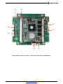
1
PCI/104-Express QSeven™ BASED SINGLE
BOARD COMPUTER
PCI/104-Express SBC with AMD Fusion G-T40E
and Integrated Data Acquisition
Rev A: July 2014
Revision
Date
A
07/16/2014
Comment
Initial Release
FOR TECHNICAL SUPPORT
PLEASE CONTACT:
[email protected]
Copyright 2014
Diamond Systems Corporation
555 Ellis Street
Mountain View, CA 94043 USA
Tel 1-650-810-2500
Fax 1-650-810-2525
www.diamondsystems.com
CONTENTS
1.
2.
3.
4.
5.
Important Safe Handling Information .............................................................................................................4
Introduction .......................................................................................................................................................6
Functional Block Diagram ...............................................................................................................................8
Board Diagram ..................................................................................................................................................9
Connector and Jumper Lists ........................................................................................................................ 11
5.1 I/O Connectors............................................................................................................................................ 11
5.2 Configuration Jumpers ............................................................................................................................... 11
6. I/O Connectors ............................................................................................................................................... 12
6.1 External Battery (J1) ................................................................................................................................... 12
6.2 PCI Bus (J2) ............................................................................................................................................... 12
6.3 Input Power (J4) ......................................................................................................................................... 13
6.4 Display Port (J5) ......................................................................................................................................... 13
6.5 HDMI (J6) ................................................................................................................................................... 14
6.6 VGA (J9) ..................................................................................................................................................... 14
6.7 SATA (J10) ................................................................................................................................................. 15
6.8 mSATA / PCIe MiniCard (J11) .................................................................................................................... 15
6.9 LVDS LCD Interface (J12, J13) .................................................................................................................. 16
6.10 LCD Backlight (J3, J24) .............................................................................................................................. 17
6.11 Data Acquisition (J14) ................................................................................................................................ 17
6.12 Ethernet (J15) ............................................................................................................................................. 18
6.13 Audio (J17) ................................................................................................................................................. 18
6.14 PCIe/104 (J20)............................................................................................................................................ 19
6.15 PS/2 Mouse and Keyboard (J21) ............................................................................................................... 20
6.16 USB Host/Client Port (J7) ........................................................................................................................... 20
6.17 USB (J25, J27) ........................................................................................................................................... 21
6.18 Serial Ports (J26, J29) ................................................................................................................................ 21
6.19 Utility Connector (J30) ................................................................................................................................ 22
6.20 Fan Connector (J31) ................................................................................................................................... 22
7. Configuration Jumpers ................................................................................................................................. 23
7.1 Battery configuration (JP1) ......................................................................................................................... 24
7.2 PCI voltage configuration (JP2) .................................................................................................................. 24
7.3 LCD Backlight Power (JP3) ........................................................................................................................ 24
7.4 RS-232/422/485 Configuration (JP4) ......................................................................................................... 25
7.5 RS-422/485 Termination configuration for COM1/2 (JP6) ......................................................................... 25
7.6 LCD Power (JP7) ........................................................................................................................................ 26
8. System Resources ......................................................................................................................................... 27
9. Video Features ............................................................................................................................................... 28
9.1 VGA CRT (J9)............................................................................................................................................. 28
9.2 Display Port (J5) ......................................................................................................................................... 29
9.3 HDMI (J6) ................................................................................................................................................... 29
9.4 LVDS (J12, J13) ......................................................................................................................................... 29
10. Updating the BIOS ......................................................................................................................................... 30
11. Installation and Configuration ...................................................................................................................... 30
11.1 Quick Setup ................................................................................................................................................ 30
11.2 Boot Device Options ................................................................................................................................... 30
12. BIOS Functions .............................................................................................................................................. 31
12.1 Access BIOS Setup: ................................................................................................................................... 31
12.2 Key Commands .......................................................................................................................................... 32
12.3 The Menus .................................................................................................................................................. 32
12.3.1 Main ................................................................................................................................................... 33
12.3.2 Advanced ........................................................................................................................................... 34
12.3.3 Chipset ............................................................................................................................................... 38
12.3.4 Boot .................................................................................................................................................... 43
12.3.5 Security .............................................................................................................................................. 44
12.3.6 Save & Exit ........................................................................................................................................ 45
13. PIC Microcontroller ........................................................................................................................................ 46
13.1 Are you there .............................................................................................................................................. 47
Quantum SBC User Manual Rev A
www.diamondsystems.com
Page 2
13.2 Configure DIO Port Command ................................................................................................................... 47
13.3 DIO Read .................................................................................................................................................... 48
13.4 DIO Output.................................................................................................................................................. 48
13.5 EEPROM Read........................................................................................................................................... 49
13.6 EEPROM WRITE........................................................................................................................................ 49
13.7 MTBF POWER CYCLE .............................................................................................................................. 50
13.8 Watchdog Timeout Set ............................................................................................................................... 51
13.9 Watchdog Trigger ....................................................................................................................................... 52
13.10 Watchdog Read .......................................................................................................................................... 52
13.11 MTBF Power Data: ..................................................................................................................................... 53
13.12 RTC Read ................................................................................................................................................... 54
13.13 RTC Write ................................................................................................................................................... 55
13.14 Set COM Mode ........................................................................................................................................... 56
13.15 Get COM Mode........................................................................................................................................... 56
13.16 READ ANALOG DATA ............................................................................................................................... 57
13.17 BOARD VOLTAGES .................................................................................................................................. 58
13.18 PWM CONTROL ........................................................................................................................................ 59
13.19 READ DIO CONFIG ................................................................................................................................... 60
13.20 CALENDAR WAKEUP ............................................................................................................................... 60
14. System Reset ................................................................................................................................................. 61
15. Data Acquisition Circuit ................................................................................................................................ 61
15.1 Protocol selection ....................................................................................................................................... 61
15.2 Application Navigation ................................................................................................................................ 62
15.3 Are You There ............................................................................................................................................ 63
15.4 Digital I/O .................................................................................................................................................... 64
15.5 EEPROM Access........................................................................................................................................ 65
15.6 Analog Data ................................................................................................................................................ 66
15.7 MTBF Data ................................................................................................................................................. 67
15.8 Watchdog.................................................................................................................................................... 68
15.9 PWM ........................................................................................................................................................... 69
15.10 RTC/Calendar ............................................................................................................................................. 70
15.11 Communication Mode ................................................................................................................................. 71
15.12 Board Voltages ........................................................................................................................................... 72
16. I/O Cables ....................................................................................................................................................... 73
17. Specifications................................................................................................................................................. 74
17.1 Processor Section (All Models) .................................................................................................................. 74
17.2 Data Acquisition Section ............................................................................................................................. 75
Quantum SBC User Manual Rev A
www.diamondsystems.com
Page 3
1. IMPORTANT SAFE HANDLING INFORMATION
WARNING!
ESD-Sensitive Electronic Equipment
Observe ESD-safe handling procedures when working with this product.
Always use this product in a properly grounded work area and wear appropriate
ESD-preventive clothing and/or accessories.
Always store this product in ESD-protective packaging when not in use.
Safe Handling Precautions
The Quantum SBC contains a high number of I/O connectors with connection to sensitive electronic components.
This creates many opportunities for accidental damage during handling, installation and connection to other
equipment. The list here describes common causes of failure found on boards returned to Diamond Systems for
repair. This information is provided as a source of advice to help you prevent damaging your Diamond Systems
(or any vendor’s) embedded computer boards.
ESD damage – This type of damage is usually almost impossible to detect, because there is no visual sign of
failure or damage. The symptom is that the board eventually simply stops working, because some component
becomes defective. Usually the failure can be identified and the chip can be replaced.
To prevent ESD damage, always follow proper ESD-prevention practices when handling computer boards.
Damage during handling or storage – On some boards we have noticed physical damage from mishandling. A
common observation is that a screwdriver slipped while installing the board, causing a gouge in the PCB surface
and cutting signal traces or damaging components.
Another common observation is damaged board corners, indicating the board was dropped. This may or may not
cause damage to the circuitry, depending on what is near the corner. Most of our boards are designed with at
least 25 mils clearance between the board edge and any component pad, and ground / power planes are at least
20 mils from the edge to avoid possible shorting from this type of damage. However these design rules are not
sufficient to prevent damage in all situations.
A third cause of failure is when a metal screwdriver tip slips, or a screw drops onto the board while it is powered
on, causing a short between a power pin and a signal pin on a component. This can cause overvoltage / power
supply problems described below. To avoid this type of failure, only perform assembly operations when the
system is powered off.
Sometimes boards are stored in racks with slots that grip the edge of the board. This is a common practice for
board manufacturers. However our boards are generally very dense, and if the board has components very close
to the board edge, they can be damaged or even knocked off the board when the board tilts back in the rack.
Diamond Systems recommends that all our boards be stored only in individual ESD-safe packaging. If multiple
boards are stored together, they should be contained in bins with dividers between boards. Do not pile boards on
top of each other or cram too many boards into a small location. This can cause damage to connector pins or
fragile components.
Power supply wired backwards – Our power supplies and boards are not designed to withstand a reverse
power supply connection. This will destroy each IC that is connected to the power supply (i.e. almost all ICs). In
this case the board will most likely will be irreparable and must be replaced. A chip destroyed by reverse power or
by excessive power will often have a visible hole on the top or show some deformation on the top surface due to
vaporization inside the package. Check twice before applying power!
Board not installed properly in PC/104 stack – A common error is to install a PC/104 board accidentally shifted
by 1 row or 1 column. If the board is installed incorrectly, it is possible for power and ground signals on the bus to
make contact with the wrong pins on the board, which can damage the board. For example, this can damage
components attached to the data bus, because it puts the 12V power supply lines directly on data bus lines.
Quantum SBC User Manual Rev A
www.diamondsystems.com
Page 4
Overvoltage on analog input – If a voltage applied to an analog input exceeds the design specification of the
board, the input multiplexor and/or parts behind it can be damaged. Most of our boards will withstand an
erroneous connection of up to 35V on the analog inputs, even when the board is powered off, but not all boards,
and not in all conditions.
Overvoltage on analog output – If an analog output is accidentally connected to another output signal or a
power supply voltage, the output can be damaged. On most of our boards, a short circuit to ground on an analog
output will not cause trouble.
Overvoltage on digital I/O line – If a digital I/O signal is connected to a voltage above the maximum specified
voltage, the digital circuitry can be damaged. On most of our boards the acceptable range of voltages connected
to digital I/O signals is 0-5V, and they can withstand about 0.5V beyond that (-0.5 to 5.5V) before being damaged.
However logic signals at 12V and even 24V are common, and if one of these is connected to a 5V logic chip, the
chip will be damaged, and the damage could even extend past that chip to others in the circuit.
Bent connector pins – This type of problem is often only a cosmetic issue and is easily fixed by bending the pins
back to their proper shape one at a time with needle-nose pliers. The most common cause of bent connector pins
is when a PC/104 board is pulled off the stack by rocking it back and forth left to right, from one end of the
connector to the other. As the board is rocked back and forth it pulls out suddenly, and the pins at the end get
bent significantly. The same situation can occur when pulling a ribbon cable off of a pin header. If the pins are
bent too severely, bending them back can cause them to weaken unacceptably or even break, and the connector
must be replaced.
Quantum SBC User Manual Rev A
www.diamondsystems.com
Page 5
2. INTRODUCTION
The Quantum SBC family integrates a QSeven™ CPU computer-on-module (COM) plus a full analog and digital
data acquisition circuit into a PCI/104-Express small form factor single board computer (SBC). It is available in the
following model:
Processor Speed
Model
CPU
QUA-GT40E-2GE
AMD G-T40E
Memory
Operating
Temperature
2GB
-20 C to +71 C
1.0GHz
o
o
The SBC includes the following key system and data acquisition features:
Processor and Memory
1GHz AMD Fusion G-T40E processor
2GB 1,333MHz 64-bit DDR3L SDRAM system memory
4GB MLC flash memory (on most models)
AMI PnP Flash BIOS (AMD models only)
Video Features
Integrated AMD Radeon HD 6250 Graphics Chipset
Display port with resolution up to 1920 x 1080
18/24-bit LVDS LCD interface with resolution up to 1920 x 1080 supports dual independent displays
VGA CRT with resolution up to 1920 x 1080
Ethernet
10/100/1000Mbps Ethernet circuit integrated in the QSeven™ CPU Module using Realtek RTL8111E
PCIe Gigabit Ethernet controller
On-board transformer and termination network for direct connection to Ethernet cabling
Standard Peripheral Interfaces
3 16550-compatible RS-232 ports (2 have RS-422/485 capability)
5 USB 2.0 ports
PS/2 keyboard and mouse ports
The BIOS supports a USB keyboard during BIOS initialization, and it also supports legacy keyboard
emulation via USB for DOS. The USB ports can be used for keyboard and mouse at the same time that
the PS/2 keyboard and mouse are connected.
HD Audio Codec from Realtek ALC262
Mass Storage
1 x Serial ATA port w/ 600MB/s HDD transfer rate on standard SATA connector
1 x Serial ATA ports w/ 600MB/s HDD transfer rate on PCIe MiniCard socket
Analog I/O
4 single-ended channels, 12-bit resolution
0-3.3V input ranges
Unipolar input ranges
Digital I/O
Up to 10 programmable digital I/O lines
Enhanced output current capability: +24mA maximum
Quantum SBC User Manual Rev A
www.diamondsystems.com
Page 6
PWM
Up to 4 programmable PWM output lines
Enhanced output current capability: +24mA maximum
Bus Interfaces
PCI-104 stackable I/O
PCIe/104 stackable I/O
1 PCIe MiniCard socket
Battery Backup
Quantum contains a backup battery for the real-time clock and BIOS settings. The battery is directly soldered to
the board and provides a minimum 7 year backup lifetime at 25°C. For longer lifetime an external battery of 3.3V
+/-10% may be attached to the board.
Power Supply
Quantum uses a wide-range input DC/DC power supply. This circuit accepts input voltages in the range of +632VDC and produces 5.0VDC +2/-0% over the full range of its expected load (7A maximum). The input power
connector provides connections for provision of +12V for LCD backlight, cooling fan, and PCI-104 connector.
Quantum SBC User Manual Rev A
www.diamondsystems.com
Page 7
3. FUNCTIONAL BLOCK DIAGRAM
Functional Block Diagram
Quantum SBC User Manual Rev A
www.diamondsystems.com
Page 8
4. BOARD DIAGRAM
The diagram below shows the board layout, including connectors and mounting holes.
J1
J2
J11
J3
J4
J5/J6
J7
J9
J10
J12
J14
J13
J15
J17
J20
J21
Quantum SBC Connector Location -- Top View
Quantum SBC User Manual Rev A
www.diamondsystems.com
Page 9
J24
J28
J25
J26
J27
J29
J30
J31
Quantum SBC Connector Location -- Bottom View with QSeven COM Attached
Quantum SBC User Manual Rev A
www.diamondsystems.com
Page 10
5. CONNECTOR AND JUMPER LISTS
5.1
I/O Connectors
Connector
5.2
Function
J1
External battery
J2
PCI bus
J3
LCD backlight A
J4
Input power
J5
Display port
J6
HDMI port
J7
USB1 host/client port
J9
VGA
J10
SATA
J11
PCIe MiniCard / mSATA
J12
LCD interface channel B (LVDS format)
J13
LCD interface channel A (LVDS format)
J14
Data acquisition I/O
J15
Ethernet
J17
Audio
J20
PCIe/104 (Port 2 and Port 3)
J21
PS/2 keyboard & mouse
J24
LCD backlight B
J25
USB 4/5
J26
Serial COM ports 1/2
J27
USB 0/2
J28
QSeven computer-on-module
J29
Serial COM port 3
J30
Utility
J31
Fan
Configuration Jumpers
Jumper
Description
JP1
Battery
JP2
PCI/104 VIN voltage configuration
JP3
LVDS display backlight voltage selection
JP4
COM 1/2 RS-422/485 configuration
JP6
COM1/2 RS-422/485 termination
JP7
LCD supply channel A & B
Quantum SBC User Manual Rev A
www.diamondsystems.com
Page 11
6. I/O CONNECTORS
Note: Pins marked as “key” are cut away or removed.
6.1
External Battery (J1)
Connector J1 is used to connect an optional external battery to replace the on-board backup battery. The onboard battery provides about 7 years of lifetime at an ambient temperature of 25⁰C. For longer lifetime an external
battery of 3.3V 10% may be connected to this connector. Diamond Systems’ cable part number 6980511 mates
with this connector.
1
2
Battery+
Ground
Connector type: Standard .1” single row straight friction lock pin header
Connector: DF13C-2P-1.25V
6.2
PCI Bus (J2)
The PCI bus connector is a solder-pin non-stack through (short pin) connector installed on the top side.
Expansion modules may be mounted only on the top side of the board due to the presence of the QSeven module
on the bottom side.
Pin
1
2
3
4
5
6
7
8
9
10
11
12
13
14
15
16
17
18
19
20
21
22
23
24
25
26
27
28
29
30
A
GND/5.0V KEY
VI/O
AD05
C/BE0*
GND
AD11
AD14
+3.3V
SERR*
GND
STOP*
+3.3V
FRAME*
GND
AD18
AD21
+3.3V
IDSEL0
AD24
GND
AD29
+5V
REQ0*
GND
GNT1*
+5V
CLK2
GND
+12V
-12V
Quantum SBC User Manual Rev A
2
B
C
D
Reserved
AD02
GND
AD07
AD09
VI/O
AD13
C/BE1*
GND
PERR*
+3.3V
TRDY*
GND
AD16
+3.3V
AD20
AD23
GND
C/BE3*
AD26
+5V
AD30
GND
REQ2*
VI/O
CLK0
+5V
INTD*
INTA*
Reserved
+5V
AD01
AD04
GND
AD08
AD10
GND
AD15
SB0*
+3.3V
LOCK*
GND
IRDY*
+3.3V
AD17
GND
AD22
IDSEL1
VI/O
AD25
AD28
GND
REQ1*
+5V
GNT2*
GND
CLK3
+5V
INTB*
Reserved
AD0
+5V
AD03
AD06
GND
M66EN
AD12
+3.3V
PAR
PME#
GND
DEVSEL#
+3.3V
CBE2#
GND
AD19
+3.3V
IDSEL2
IDSEL3
GND
AD27
AD31
VI/O
GNT0*
GND
CLK1
GND
RST*
INTC*
GND
www.diamondsystems.com
Page 12
Connector:
PCI-104 non-stack-through with solder pins; bottom side shroud and shroud mounting holes not
required
Mating connector:
6.3
Any PCI-104 stack-through connector
Input Power (J4)
Quantum SBCs accept a wide-range input DC/DC power supply. This circuit accepts input voltages in the range
of +6-32VDC. All other required voltages are generated on board. Each pin is rated at 3A max. Diamond Systems’
cable part number 6980510 mates with this connector.
Additional 12V power rails required by for LCD backlight, cooling fan, and PCI-104 connector (if needed) is
provided on connector J4.
1
2
3
4
5
+6-34VDC
+6-34VDC
Ground
Ground
+12V In
Connector type: Standard .1” single row, 5 positions, straight pin header with gold flash plating
Connector: IPL1-105-01-L-S-K
6.4
Display Port (J5)
The Quantum SBC provides a standard display port on connector J5. The resolution of the display port output
matches the resolution configured in the display port. An attached monitor should be able to automatically adapt
for many of the available resolutions.
Display Port Connector J5
Lane 0+
Lane 0Ground
Lane 2+
Lane 2Ground
Ground
Aux+
AuxPower return
1
3
5
7
9
11
13
15
17
19
Signal Name
Lane 0+/- to Lane 3+/Ground
AUX +/Hot Plug Detect
3.3V
2
4
6
8
10
12
14
16
18
20
Ground
Lane 1+
Lane 1Ground
Lane 3+
Lane 3Ground
Ground
Hot Plug Detect
3.3V
Definition
Main link
Ground return
Auxiliary channel
Hot Plug Detect
Power
Connector type: Standard Display Port connector, PC mount right angle
Quantum SBC User Manual Rev A
www.diamondsystems.com
Page 13
6.5
HDMI (J6)
Freescale A9 i.MX6 Quantum SBC models provide a standard HDMI on connector J6. The resolution of the HDMI
output matches the resolution configured in the HDMI monitor. An attached monitor should be able to
automatically adapt for many of the available resolutions.
HDMI connector J6
Data 2+
Data 2Ground
Data 0+
Data 0Ground
CEC (NC)
DDC Clock
Ground
Hot Plug Detect
1
3
5
7
9
11
13
15
17
19
Signal Name
Data 0+/- to Data 3+/Ground
Clock +/DDC-CLOCK/DATA
Hot Plug Detect
+5V
2
4
6
8
10
12
14
16
18
Ground
Data 1+
Data 1Ground
Clock+
ClockReserved
DDC Data
+5V
Definition
TDMS data pair
Ground return
TDMS data pair
Signals used for monitor detection (DDC1 specification)
Hot Plug Detect
Power
Connector type: Standard HDMI type A connector, PC mount right angle
6.6
VGA (J9)
Connector J9 is used to connect a VGA monitor. Although the DDC serial detection pins are present, a 5V power
supply is not provided, and the legacy “Monitor ID” pins are also not used. Diamond Systems’ cable part number
6980507 mates with this connector.
RED
Ground
GREEN
Ground
BLUE
Ground
HSYNC
VSYNC
Ground
DDC-Data
DDC-Clock
Ground
1
2
3
4
5
6
7
8
9
10
11
12
Signal Name
RED
Ground
GREEN
BLUE
DDC-CLOCK/DATA
Quantum SBC User Manual Rev A
Definition
RED signal (positive, 0.7Vpp into 75 Ohm load)
Ground return for RED, GREEN, and BLUE signals
GREEN signal (positive, 0.7Vpp into 75 Ohm load)
BLUE signal (positive, 0.7Vpp into 75 Ohm load)
Signals used for monitor detection (DDC1 specification)
www.diamondsystems.com
Page 14
Connector type: Standard 2mm single row straight pin header with gold flash plating.
Connector: JST BM12B-GHS-TBT 1x12 vertical SMT
6.7
SATA (J10)
This connector avails the SATA connection on the carrier boards.
1
2
3
4
5
6
7
Ground
SATA 1 TX+
SATA 1 TXGround
SATA 1 RXSATA 1 RX+
Ground
Connector type: Standard 7-pin SATA connector, right angle
Connector: Molex 470804005
6.8
mSATA / PCIe MiniCard (J11)
This socket can be configured for either PCIe MiniCard or mSATA disk module use. The configuration is done
with 0 ohm resistors where a conflict occurs between the two configurations as shown in bold.
PCIe MiniCard
ClkreqGnd
PCIe ClkPCIe Clk+
Gnd
mSATA
Gnd
PCIe 1 ClkPCIe 1 Clk+
Gnd
Gnd
Gnd
PCIe 0 RXPCIe 0RX+
SATA 1 RXSATA 1 RX+
Gnd
Gnd
Gnd
Gnd
PCIe 0 TXPCIe 0 TX+
SATA 1 TXSATA 1 TX+
Gnd
Gnd
+3.3V
+3.3V
Ground
Gnd
Gnd
+3.3V
+3.3V
Ground
Pull-up to +3.3V
Pull-up to +3.3V
Quantum SBC User Manual Rev A
mSATA / PCIe MiniCard
1
2
3
4
5
6
7
8
9
10
11
12
13
14
15
16
KEY
17
18
19
20
21
22
+3.3V
Gnd
+1.5V
23
24
+3.3V
25
27
29
26
28
30
Gnd
+1.5V
SMB Clk
31
32
SMB Data
33
35
37
39
41
43
45
47
49
51
34
36
38
40
42
44
46
48
50
52
Gnd
USB 4USB 4+
Gnd
WWAN LED#WLAN LED#
WPAN LED#
+1.5V
Gnd
+3.3V
Gnd
W_Disable#
PCIe Reset#-
www.diamondsystems.com
Page 15
Note: For mSATA mode, the PCIe clock signal is not active because CLKREQ- pin is not driven low by the
module.
Connector: JAE MM60-52B1-E1-R650 mSATA / PCIe MiniCard socket
JAE NT4R1600 3.55mm high M2 x 0.4 threaded mounting spacers qty 2 built into baseboard for fullsize module
6.9
LVDS LCD Interface (J12, J13)
Connector J13 is used to connect LVDS LCD Channel A. Connector J12 is used to connect LVDS LCD Channel
B. Voltage selection for LCD can be configured on JP7. If needed, the LCD backlight can be connected to
connector JP3. Diamond Systems’ cable part number 6981211 mates with these connectors for LCD connection.
J13, LCD Channel A
A3+
A3Signal Ground
A1+
A1Signal Ground
Channel A Clk+
Channel A ClkSignal Ground
DID_DAT
1
3
5
7
9
11
13
15
17
19
2
4
6
8
10
12
14
16
18
20
A2+
A2Signal Ground
A0+
A0Signal Ground
Vcc 3.3V / 5V (jumper configured)
Vcc 3.3V / 5V (jumper configured)
Signal Ground
DID_CLK
J12, LCD Channel B
B3+
B3Signal Ground
B1+
B1Signal Ground
Channel A Clk+
Channel A ClkSignal Ground
DID_DAT
1
3
5
7
9
11
13
15
17
19
2
4
6
8
10
12
14
16
18
20
B2+
B2Signal Ground
B0+
B0Signal Ground
Vcc 3.3V / 5V (jumper configured)
Vcc 3.3V / 5V (jumper configured)
Signal Ground
DID_CLK
Connector type: Standard 2mm dual row straight pin header with gold flash plating.
Connector: Channel A: JST BM20B-GHDS-G-TF 2x10 straight 1.25mm pitch gold
Channel B: JST BM20B-GHDS-G-TF 2x10 straight 1.25mm pitch gold
Mating connector: JST GHDR-20V-S
Crimp terminal: JST SGHD-002GA-P0.2
Quantum SBC User Manual Rev A
www.diamondsystems.com
Page 16
6.10 LCD Backlight (J3, J24)
Connector J3 provides the backlight power for LCD Channel A Connector. J24 provides the backlight power for
LCD Channel B and control for an optional LCD panel. Diamond Systems’ cable part number 6981210 mates with
this connector.
J3, LCD Backlight Channel A
1
2
3
4
5
6
LCD A Power
LCD A Power
Ground
Ground
Enable (GPIO output), 0 = off, open circuit = on
Brightness, 0-5VDC variable; 0V = max, 5V = min
J24, LCD Backlight Channel B
1
2
3
4
5
6
LCD B Power
LCD B Power
Ground
Ground
Enable (GPIO output), 0 = off, open circuit = on
Brightness, 0-5VDC variable; 0V = max, 5V = min
The LCD power is jumper selectable for +5V or +12V. See the description for JP3.
The enable signal controls power to the backlight. It is controlled by digital I/O signal.
Connector Part Numbers: Molex 53398-0671
6.11 Data Acquisition (J14)
Connector J14 provides 10 digital I/O lines from PIC controller. These lines have ESD protection to protect the
SBC from potential damage. The connector also provides four analog input channels and four pulse width
modulator outputs. Diamond Systems’ cable part number 6980501 mates with this connector.
DIO 0
DIO 2
DIO 4
DIO 6
DIO 8
PWM 1A
PWM 1C
Ground
AN0
AN2
Signal
DIO 0-9
PWM 1A:1D
AN 0:3
Ground
Agnd
1
3
5
7
9
11
13
15
17
19
2
4
6
8
10
12
14
16
18
20
DIO 1
DIO 3
DIO 5
DIO 7
DIO 9
PWM 1B
PWM 1D
Agnd
AN1
AN3
Definition
Digital I/Os
PWM outs
Analog inputs
Digital ground
Analog ground
Connector type: Standard 2mm dual row straight pin header with gold flash plating
Connector: JST BM20B-GHDS-G-TF 2x10 straight 1.25mm pitch gold
Quantum SBC User Manual Rev A
www.diamondsystems.com
Page 17
6.12 Ethernet (J15)
The 10/100/1000 Base-T, full-duplex Ethernet interface is provided by connector J15. Diamond Systems’ cable
part number 6980502 mates with this connector.
MX1+
MX1MX2+
MX2MX3+
MX3MX4+
MX4NC
Ground
1
2
3
4
5
6
7
8
9
10
Signal
TX+, TXRX+, RXGround
Definition
Transmit data from Q7 connector
Receive data by Q7 connector
System ground
Connector type: Standard 2mm single row straight pin header with gold flash plating
Connector: JST BM10B-GHS-TBT 1x10 vertical SMT
6.13 Audio (J17)
Quantum provides an HDA audio circuit based on the Realtek ALC262 audio chip. The circuit offers stereo line in,
stereo line out, and mono mic in connections. Diamond Systems’ cable part number 6980508 provides the 3.5
mm output and input jacks for Lineout, Mic and Line in connection.
1
2
3
4
5
6
7
8
LineOut – L
LineOut – R
GND_Audio
LineIn – L
LineIn – R
GND_Audio
MIC IN
GND_Audio
Connector: JST BM08B-GHS-TBT 1x8 vertical SMT
Quantum SBC User Manual Rev A
www.diamondsystems.com
Page 18
6.14 PCIe/104 (J20)
The PCIe/104 (J20) connector is a 1-bank version of the PCIe/104 connector, providing only the first bank of pins
numbered 1-52. It offers up to two PCIe x1 lanes from ports 2 and 3 of the QSeven module (third and fourth
lanes) plus up to two USB ports from ports 6 and 7 of the QSeven module (seventh and eighth ports). It also
provides connections for SMB signals from the QSeven module.
PCIe/104 SpecificationCarrier
USB-OC+3.3V
USB 1+
USB 1Gnd
PCIe 1 T+
PCIe 1 TGnd
PCIe 2 T+
PCIe 2 TGnd
PCIe 1 R+
PCIe 1 RGnd
PCIe 2 R+
PCIe 2 RGnd
PCIe 1 Clk+
PCIe 1 Clk+5V_STBY
PCIe 2 Clk+
PCIe 2 ClkDir
SMB Data
SMB Clk
SMB Alert-
Carrier
USB-OC+3.3V
USB 7+
USB 7Gnd
PCIe 3 T+
PCIe 3 TGnd
Gnd
PCIe 3 R+
PCIe 3 RGnd
Gnd
PCIe 3 Clk+
PCIe 3 Clk+5V_STBY
Dir
SMB Data
SMB Clk
SMB Alert-
PCIe/104 Specification
1
3
5
7
9
11
13
15
17
19
21
23
25
27
29
31
33
35
37
39
41
43
45
47
49
51
+
5
V
T
A
B
2
4
6
8
10
12
14
16
18
20
22
24
26
28
30
32
34
36
38
40
42
44
46
48
50
52
PCIe Reset+3.3V
USB 6+
USB 6Gnd
PCIe 2 T+
PCIe 2 TGnd
Gnd
PCIe 2 R+
PCIe 2 RGnd
Gnd
PCIe 2 Clk+
PCIe 2 Clk+5V_STBY
PU to 3.3V
PCIe Reset+3.3V
USB 0+
USB 0Gnd
PCIe 0 T+
PCIe 0 TGnd
PCIe 3 T+
PCIe 3 TGnd
PCIe 0 R+
PCIe 0 RGnd
PCIe 3 R+
PCIe 3 RGnd
PCIe 0 Clk+
PCIe 0 Clk+5V_STBY
PCIe 3 Clk+
PCIe 3 ClkPwr Good
PCIe x16 Clk+
PCIe x16 ClkPSON-
Connector: Samtec ASP-129637-08 QMS series 15.24mm stacking height single bank
Mating connector: Samtec ASP-129646-18 QFS series 15.24mm stacking height single bank or ASP-129646-03
QFS series 15.24mm stacking height 3-bank connector
Quantum SBC User Manual Rev A
www.diamondsystems.com
Page 19
6.15 PS/2 Mouse and Keyboard (J21)
Connector J21 provides the standard PS/2 keyboard and mouse signals. Diamond Systems’ cable part number
6980506 mates with this connector and provides standard connections for PS/2 keyboard and mouse.
+5V
KB Data
KB Clk
Ground
+5V
MS Data
MS Clk
Ground
Signal
+5V
KB Data
KB Clk
MS Data
MS Clk
Ground
Key
1
2
3
4
5
6
7
8
Definition
System +5V power
Keyboard data
Keyboard clock
Mouse data
Mouse clock
System ground
Key pin (missing on pin header, plugged on mating cable)
Connector type: Standard 2mm single row right angled pin header with gold flash plating
6.16 USB Host/Client Port (J7)
Quantum features one USB Host / Client port on connector J7. Port 1 may be a client port on some of the Q7
modules. J7 interfaces to USB port 1. USB 2.0 provides a 480Mbps maximum data transfer rate. The shield pin
on each connector is tied to system ground. Diamond Systems’ cable part number 6980504 mates with these
connectors for Host. Diamond Systems’ cable part number 6980505 mates with these connectors for Client.
1
2
3
4
5
USB0 Power
USB0 DataUSB0 Data+
Ground
Device ID
Connector: JST BM05B-GHS-TBT 1x5 vertical SMT (ports 1), top side of PCB
Mating connector: JST GHR-5V-S
Quantum SBC User Manual Rev A
www.diamondsystems.com
Page 20
6.17 USB (J25, J27)
Quantum features four USB 2.0 ports on 2 pin headers. Connector J25 interfaces to USB port 4/5 and connector
J27 interfaces to USB ports 0/2. USB 2.0 provides a 480Mbps maximum data transfer rate. The shield pin on
each connector is tied to system ground. Diamond Systems’ cable number 6980503 mates with these connectors.
J27, USB ports 0 and 2
USB0 Pwr
USB0 DataUSB0 Data+
Ground
Shield
USB2 Pwr
USB2 DataUSB2 Data+
Ground
Shield
1
2
3
4
5
6
7
8
9
10
J25, USB ports 4 and 5
USB4 Pwr
USB4 Data+
USB4 DataGround
Shield
USB5 Pwr
USB5 Data+
USB5 DataGround
Shield
1
2
3
4
5
6
7
8
9
10
Connector type: Standard 2mm single row right angled pin header with gold flash plating
Connector: JST SM10 B-GHS-TBT 1x10 right angled SMT
6.18 Serial Ports (J26, J29)
There are two serial port connectors with identical pin outs. Ports 1-2 are on J26 connector and port 3 is on the
bottom side right angled J29 connector. RS-422 and RS-485 pin outs apply only to ports 1 and 2. Diamond
Systems’ cable number 6980500 provides two DB9 connectors.
Pin RS-232
RS-422
RS-485
1
2
3
4
5
6
7
8
9
10
TX1+
TX1RX1+
RX1Ground
TX2+
TX2RX2+
RX2Ground
TX/RX 1+
TX/RX 1NC
NC
Ground
TX/RX 2+
TX/RX 2NC
NC
Ground
TX1
RTS1
RX1
CTS1
Ground
TX2
RTS2
RX2
CTS2
Ground
Port 3 only provides RS-232 protocol. Ports 1 and 2 also provide RS-422/485 capability.
Connector: JST SM10B-GHS-TB 1x10 right angle SMT, located on bottom side of PCB
Quantum SBC User Manual Rev A
www.diamondsystems.com
Page 21
6.19 Utility Connector (J30)
The pin out of the utility connector is shown below along with the corresponding QSeven module connector pin.
Diamond Systems’ cable number 6980509 mates with these connectors.
QSeven Pin
20
21
13
8
Signal
Gnd
Pwr SwitchSleepGBE LinkGBE Link1000-
Signal
1
3
5
7
9
2
4
6
8
10
QSeven Pin
ResetWDT TriggerBattery LowGBE Link100+3.3V (fused)
28
70
27
7
Connector: 2mm pitch 2x5 vertical pin header, 4mm posts, gold plating
Mating connector: 2mm pitch 2x5 IDC or crimp terminal socket
6.20 Fan Connector (J31)
The pin out of the fan connector is shown below. The fan is powered by +5VDC.
PWMOUT
Tacho_In
Power 5V
Ground
1
2
3
4
Connector: Molex 0532610471
Connector type: Standard .1” single row straight pin header with gold flash plating
Quantum SBC User Manual Rev A
www.diamondsystems.com
Page 22
7. CONFIGURATION JUMPERS
The Quantum SBC contains the following configuration jumper blocks. The diagram below shows the default
jumper settings.
Jumper
Description
JP1
Battery
JP2
PCI voltage configuration
JP3
LCD backlight power
JP4
COM 1/2 RS-232/422/485 configuration
JP6
COM 1/2 RS-422/485 termination configuration
JP7
LCD supply channel A & B
JP1
JP2
JP3
JP4
JP6
JP7
Quantum SBC User Manual Rev A
www.diamondsystems.com
Page 23
7.1
Battery configuration (JP1)
Jumper block JP1 configures the battery voltage supply.
Battery Jumper JP1
VBAT_IN
VCC_RTC
7.2
1
2
Pins 1-2
Function
Jumper
VIO_RTC = 3V
No jumper
VCC_RTC = 0V
PCI voltage configuration (JP2)
Jumper block JP2 configures the voltage supply for PCI/104 add on modules.
VIO_PCI Jumper JP2
5V
VIO_PCI
3.3V
7.3
1
2
3
JP2
Function
1-2
VIO_PCI = 5V
2-3
VIO_PCI = 3.3V
LCD Backlight Power (JP3)
Jumper block JP3 configures the voltage supply for the LCD backlight. There are labels on the board representing
the jumper configurations. Available options are +5V input or +12V.
LCD Backlight Power JP3
12V
VLCD_BKLT A
5V
5V
VLCD_ BKLT B
12V
1
2
3
4
5
6
JP3
Function
1-2
VLCD_BKLT A = 12V
2-3
VLCD_BKLT A = 5V (Default)
4-5
VLCD_BKLT B = 5V (Default)
5-6
VLCD_BKLT B = 12V
Quantum SBC User Manual Rev A
www.diamondsystems.com
Page 24
7.4
RS-232/422/485 Configuration (JP4)
Use JP4 to set COM1 and COM 2 in RS-232/422/485 modes.
RS-232/422/485 Jumper JP4
1
2
3
4
5
6
7
8
W_DISABLE
GROUND
MODE 0
GROUND
MODE 2
GROUND
PIC_MCLR_RESET
PIC_MCLR_RC
MODE 0
7.5
MODE 2
Function
3-4 jumper (Default)
5-6 Open - No jumper
(Default)
RS-232 Mode ( Default)
3-4 Open - No jumper
5-6 Open - No jumper
2T/2R RS-422
3-4 Open - No jumper
5-6 jumper
2T/2R RS-485 & 2R RS-232
3-4 jumper
5-6 jumper
Loop Back Mode (TX in to RX out )
RS-422/485 Termination configuration for COM1/2 (JP6)
Use JP6 to select the COM1 RS-422/485 termination and COM2 RS-422/485 termination. Any port configured for
RS-232 should not have any jumpers installed.
For RS-422: Installing two jumpers in the 422 TERM positions connects a 120 ohm termination resistor across
the RX + and – lines and connects 1K ohm bias resistors to the RX lines. The + line is biased toward ground, and
the – line is biased toward +5V. This sets the receiver to an inactive state when the receiver is unconnected. Both
jumpers should be installed if termination / biasing is desired. Installing only one jumper will create unpredictable
behavior by the receiver.
For RS-485: Installing a jumper in the 485 TERM position connects a 120 ohm resistor across the differential
driver/receiver pair. The RS-485 network should have a termination resistor installed at each end of the circuit but
not at intermediate nodes.
RS-422/485 Termination JP6
RX1+
RX1RX2+
RX2-
1
2
3
4
JP6
Function
1-2 jumper
120 ohm on Port1
1-2 Open - No jumper
No Termination - Default
3-4 jumper
120 ohm on Port2
3-4 Open - No jumper
No Termination - Default
Quantum SBC User Manual Rev A
www.diamondsystems.com
Page 25
7.6
LCD Power (JP7)
Jumper block JP7 configures the voltage supply for the LCD. There are labels on the board representing the
jumper configurations. Available options are +3.3V input or +5V.
LCD Power JP7
5V
VLCD_ A
3.3V
3.3V
VLCD_ B
5V
1
2
3
4
5
6
JP3
Function
1-2
VLCD_ A = 5V
2-3
VLCD_ A =3.3 (Default)
4-5
VLCD_ B = 3.3V (Default)
5-6
VLCD_ B = 5V
Quantum SBC User Manual Rev A
www.diamondsystems.com
Page 26
8. SYSTEM RESOURCES
The table below lists the default system resources utilized by the circuits on Quantuam SBC.
Device
I/O Address
ISA IRQ
ISA DMA
Serial Port COM1
0x3F8 – 0x3FF
4
–
Serial Port COM2
0x2F8 – 0x2FF
3
–
Serial Port COM3
0x3E8 – 0x3EF
10
–
Serial Port COM4
0x2E8 – 0x2EF
11
–
Ethernet
OS-dependent
OS-dependent
–
USB
OS-dependent
OS-dependent
–
Sound
OS-dependent
OS-dependent
–
Video
OS-dependent
OS-dependent
–
PC/104-Plus
OS-dependent
OS-dependent
–
PCIe/104
OS-dependent
OS-dependent
–
mini PCIe
OS-dependent
OS-dependent
–
Most of these resources are configurable and, in many cases, the operating system alters these settings. The
main devices that are subject to this dynamic configuration are on-board Ethernet, sound, video, USB, and any
PC/104-Plus cards, PCIe/104, and PCIe MiniCards that are in the system. These settings may also vary
depending on what other devices are present in the system. For example, aDisplay Port ng on a PC/104-Plus
card may change the on-board Ethernet resources.
Quantum SBC User Manual Rev A
www.diamondsystems.com
Page 27
9. VIDEO FEATURES
The Quantum SBC includes a video subsystem that provides Display Port, HDMI, CRT and 2 LVDS output with
several choices of resolution. The resolution is can be changed in the BIOS.
LVDS Resolution
CRT Auto-Adapt
640 x 480 18Bit Single
Yes
800 x 600 18Bit Single
Yes
Note
1024x 600 18Bit Single
1024 x 768 18Bit Single
Yes
Default resolution
1280 x 720 18Bit Single
1280 x 800 18Bit Single
1366 x 768 18Bit Single
1440 x 900 18Bit Single
1366 x 768 24Bit Single
1440 x 900 24Bit Single
1280 x 1024 24Bit Dual
1440 x 1050 24Bit Dual
1600 x 900 24Bit Dual
1680 x 1050 24Bit Dual
1600 x 1200 24Bit Dual
1920 x 1080 24Bit Dual
9.1
VGA CRT (J9)
The Quantum SBC provides a standard CRT port on connector J8. The resolution of the CRT output matches the
resolution configured in the BIOS for the LVDS/CRT. An attached monitor should be able to automatically adapt
for many of the available resolutions. If the monitor does not adapt properly, either adjust the monitor settings,
change the LVDS/CRT resolution in the BIOS (see BIOS section), or use a different monitor.
Note: The BIOS setup screens and DOS display are always configured for 640x480 resolutions, regardless of the
display resolution selected in the BIOS. If you configure the BIOS for a different resolution, the display may not
look correct when you are in the BIOS setup screens or in DOS. For example, if the screen is set for 1024x768,
the BIOS and DOS screens will appear smaller than full screen and will generally be centered in the screen with a
blank border around them. If you are using DOS, the optimum CRT resolution is 640x480. This same advice may
apply for a text-based Linux environment as well.
Diamond Systems cable number 6980507 is used to connect a monitor to connector J9. It provides a standard
DB15 female connector for a CRT.
Quantum SBC User Manual Rev A
www.diamondsystems.com
Page 28
9.2
Display Port (J5)
The Quantum SBC provides a standard display port on connector J5. The resolution of the display port output
matches the resolution configured in the display port. An attached monitor should be able to automatically adapt
for many of the available resolutions.
9.3
HDMI (J6)
Quantum provides a standard HDMI on connector J6. The resolution of the HDMI output matches the resolution
configured in the HDMI monitor. An attached monitor should be able to automatically adapt for many of the
available resolutions.
9.4
LVDS (J12, J13)
The LCD used with the Quantum SBC must match the programmed resolution and scan rate in the BIOS. These
settings can be changed in BIOS. Quantum provides 18-bit/24 bit LVDS output, so the LCD selected must work
with 18-bit /24 bit data.
As opposed to CRTs, there is no standard LCD connector type or format. Each LCD manufacturer has its own
standards, and there are also different specifications such as the number of data bits used in the video signal.
You may need to create your own LCD cable to connect from the LCD connector on Quantum to the input
connector on your LCD. For assistance with signal definitions or wiring requirements, contact the LCD maker or
Diamond Systems technical support. Diamond Systems offers cable part number 6981211 with the correct
connector type and pinout to match the LCD connector on the Quantum SBC. The other end may need to be
changed to work with your LCD.
Connector J13 is used to connect LVDS LCD Channel A. Connector J12 is used to connect LVDS LCD Channel
B. Voltage selection for LCD can be configured on JP7. If needed, the LCD backlight can be connected to
connector JP3.
The backlight power is jumper-selectable between +5V and +12V using jumper block JP3. If 12VDC is needed for
the LCD, it must be provided either on one of the input power connectors or on the 12V pin (J1, B9) of the PC/104
connector. Quantum does not generate 12V internally.
WARNING: Be sure the proper voltage is configured BEFORE connecting the cable to your backlight inverter, or
it could be damaged.
The brightness control for the LCD backlight has a weak pull-down resistor to ensure maximum brightness when it
is not connected externally.
Diamond Systems offers cable part number 6981210 with the correct connector type and pin out to match the
backlight power connector on Quantum SBC. The other end may need to be changed to work with your LCD
backlight inverter.
Quantum SBC User Manual Rev A
www.diamondsystems.com
Page 29
10. UPDATING THE BIOS
The BIOS image is programmed into the Quantum SBC by using the SPIFLASH utility program.
1. Create a DOS bootable mass storage device such as a USB memory stick.
2. Copy the desired BIOS image file to the boot device.
3. Install the boot device on the Quantum SBC and power it up.
4. At the DOS prompt, type the following command. <filename.bat> is the name of the BIOS image file. The
filename must conform to the DOS 8-character naming convention.
Run <filename.bat>
5. SPIFLASH will automatically reprogram the SBC’s BIOS image and provide a progress indicator. The
program will indicate successful completion of the process, which should take about 10 seconds.
6. Restart the system and press the DEL key to enter the BIOS SETUP utility.
7. Hit the left arrow key once to go to the tab labeled “Exit.” Select “Load optimal defaults” using the up/down
arrow keys, and hit Enter to confirm. Then select “Save and Exit,” and hit Enter to confirm.
8. This completes the BIOS process. Reboot the system with the LCD attached to verify proper performance.
11. INSTALLATION AND CONFIGURATION
This section describes the steps needed to get your Quantum SBC up and running, and assumes that you have
the Quantum Development Kit or Quantum Cable Kit. The Cable Kit includes all cables needed for the I/O. The
Development Kit includes the SBC, Cable Kit, and AC adapter to power the SBC.
11.1 Quick Setup
1. Attach VGA cable 6980507, PS/2 keyboard / mouse cable 6980508, and USB cables 6980503 as
needed.
2. Attach display, keyboard, and mouse (if needed) to the cables.
3. Connect power to power input connector J4 using AC adapter X or your own power supply with power
cable 6980510. The input connector and cable keyed to prevent incorrect connection. However ensure
that the red wire +5V are on pin 1 of the board connector J4.
WARNING: Attaching the power connector incorrectly will destroy the QUANTUM SBC!
4. For a quick verification that the system is set up and working properly, if no boot device is attached, the
system will boot to BIOS screen.
11.2 Boot Device Options
Quantum can boot from a SATA, mSATA, or USB device. The boot device selection and priority are configured in
the BIOS Boot menu. See Chapter 12 for detailed BIOS instructions. Only devices which are currently attached to
the SBC will appear in the list of options. Therefore if you want to select a hard drive or USB device as the boot
device, you must connect it to the SBC first, then boot up and enter the BIOS, then select it as a boot device.
The following are a few example boot scenarios.
Install an SATA hard disk directly on the SATA connector.
Attach a bootable USB device to one of the USB ports with USB cable part number 6980503.
Quantum SBC User Manual Rev A
www.diamondsystems.com
Page 30
12. BIOS FUNCTIONS
The BIOS on the Quantum SBC provides access to many valuable features. These instructions show how to
enter the BIOS, set up features, and restore the BIOS to its default settings.
The BIOS Setup utility controls BIOS settings and configures various system features. The system settings are
stored in the system’s BIOS ROM. And the BIOS is activated once the computer powers on.
12.1 Access BIOS Setup:
To access the BIOS Setup, follow the steps below:
1. Connect the Quantum SBC to a monitor.
2. Turn on the monitor.
3. Supply power to the Quantum SBC.
4. Continuously press the Delete key once the computer powers on until the BIOS Setup utility opens.
Whatever menu or submenu is selected thereafter, the menu or submenu is presented in two panes onscreen.
The left pane displays all the settings that are accessible to users while the right pane shows the setting direction.
Each menu offers a set of appropriate settings. When a setting is selected on the left pane, it becomes highlighted
in white. Available settings are enclosed in brackets while the non-settings are presented in dark gray.
Quantum SBC User Manual Rev A
www.diamondsystems.com
Page 31
12.2 Key Commands
The BIOS Setup utility relies on a keyboard to receive user’s instructions. Use the following keys to use the utility.
Note a “WARNING” shows in the left pane onscreen when making any change to the BIOS settings.
12.3 The Menus
The Quantum SBC features the BIOS Setup with six menus, which are explained hereafter in this chapter.
Quantum SBC User Manual Rev A
www.diamondsystems.com
Page 32
12.3.1 Main
The Main menu displays some important BIOS and memory information and features the settings of System Date
and System Time.
The displayed info is:
The featured settings are:
Quantum SBC User Manual Rev A
www.diamondsystems.com
Page 33
12.3.2 Advanced
Use the Advanced menu to control the system’s PCI, ACPI, IDE, USB and Super I/O.
The featured settings and submenus are:
Quantum SBC User Manual Rev A
www.diamondsystems.com
Page 34
PCI Subsystem Settings
This submenu configures PCI, PCI-X and PCI Express. The featured settings and submenus are:
ACPI Settings
ACPI Settings configure the system’s ACPI (Advanced Configuration and Power Interface). The featured settings
are:
Quantum SBC User Manual Rev A
www.diamondsystems.com
Page 35
IDE Configuration
Select IDE Configuration to view the system’s status of IDE, i.e. the integrated device interface, a type of diskdrive interface in which the controller electronics reside on the drive itself to eliminate the need for a separate
adapter card.
USB Configuration
USB Configuration displays the info of the connected USB devices and configures USB parameters. The featured
settings are:
Quantum SBC User Manual Rev A
www.diamondsystems.com
Page 36
SCH3114 Super I/O Configuration
SCH3114 Super I/O Configuration is a submenu to configure the system’s Super IO chip SMSC SCH3114 to
optimize the serial ports on the system. The featured submenus are:
Quantum SBC User Manual Rev A
www.diamondsystems.com
Page 37
12.3.3 Chipset
This menu configures the system’s chipset features including bus speed management, graphics and the access
to the system memory. The chipset also coordinates the communications with the PCI bus.
The featured submenus are North Bridge, North Bridge LVDS Config Select, and South Bridge which are
explained in the following of this section.
North Bridge
This submenu configures the system’s north bridge features including graphics, memory and socket 0. This
submenu also presents some important memory information. The featured settings and submenus are:
Quantum SBC User Manual Rev A
www.diamondsystems.com
Page 38
GFX Configuration
This submenu features the following settings to configure the system’s graphics:
Quantum SBC User Manual Rev A
www.diamondsystems.com
Page 39
Memory Configuration
This submenu features the following settings to configure the system’s memory:
Socket 0 Information
Socket 0 Information enables viewing the CPU’s Socket 0 information such as the starting/ending address and
the presence or absence of memory modules in the DIMM slots.
Quantum SBC User Manual Rev A
www.diamondsystems.com
Page 40
North Bridge LVDS configuration Select
This submenu features the following settings to configure the INT15 options for the LVDS:
South Bridge
Select this submenu to view the south bridge’s CIM version and to configure its features.
Quantum SBC User Manual Rev A
www.diamondsystems.com
Page 41
SB SATA Configuration
Use this submenu to configure the system’s SATA feature by the following settings:
SB USB Configuration
Use this submenu to configure the system’s USB features:
Quantum SBC User Manual Rev A
www.diamondsystems.com
Page 42
12.3.4 Boot
The Boot menu configures how to boot the system by defining boot device priority.
The settings are:
Quantum SBC User Manual Rev A
www.diamondsystems.com
Page 43
12.3.5 Security
The Security menu sets up an administrator password to limit access to the BIOS Setup utility. Users will be
asked for the password each time he/she tries to access the BIOS Setup utilities.
The setting is:
Quantum SBC User Manual Rev A
www.diamondsystems.com
Page 44
12.3.6 Save & Exit
The Save & Exit menu features a handful of commands to launch actions from the BIOS Setup utility regarding
saving changes, quitting the utility and recovering defaults.
The settings are:
Quantum SBC User Manual Rev A
www.diamondsystems.com
Page 45
13.
PIC MICROCONTROLLER
The Quantum SBC contains a PIC microcontroller that is used to provide various functions including serial port
configuration, general purpose I/O lines, A/D lines, pulse width modulators, generate wake events, and others.
This section describes the command sets that can be used to communicate with the PIC controller.
The list below describes the constants that have been used in this section.
MESSAGE_SIG
0x3232
COMMAND_AREYOU
0x01
COMMAND_WRITE_EPROM
0x03
COMMAND_READ_EPROM
0x05
COMMAND_CONFIG_DIOPORT
0x07
COMMAND_DIO_OUTPUT
0x09
COMMAND_DIO_READ
0x0B
COMMAND_ANALOG_READ
0x0D
COMMAND_CONFIG_PWM
0x0F
COMMAND_WATCHDOG_SET
0x17
COMMAND_WATCHDOG_READ
0x19
COMMAND_WATCHDOG_TRIGGER
0x1B
COMMAND_CALENDAR_WAKEUP
0x1D
COMMAND_MTBF_DATA
0x1F
COMMAND_MTBF_POWER
0x21
COMMAND_RTC_READ
0x23
COMMAND_RTC_WRITE
0x25
COMMAND_SET_COM_MODE
0x27
COMMAND_GET_COM_MODE
0x29
COMMAND_BOARD_VOLTAGE
0X2B
COMMAND_CONFIG_READ_DIOPORT
0x2F
COMMAND_RECEIVER_AREYOUTHERE
0x02
COMMAND_RECEIVER_EPROMDATA
0x04
COMMAND_RECEIVER_DIODATA
0x0C
COMMAND_RECEIVER_ANALOG_DATA
0x0E
COMMAND_RECEIVER_WATCHDOG_SETTINGS 0x1A
COMMAND_RECEIVER_ACK
0x1C
COMMAND_RECEIVER_MTBF_DATA
0x1E
COMMAND_RECEIVER_MTBF_POWER
0x20
COMMAND_RECEIVER_RTC_DATA
0x22
COMMAND_RECEIVER_GET_COM_MODE
0x24
COMMAND_RECEIVER_BOARD_VOLTAGE
0X26
COMMAND_RECEIVER_CONFIG_READ_DIOPORT
0x2A
Quantum SBC User Manual Rev A
www.diamondsystems.com
Page 46
13.1
Are you there
Command Description:
Byte
Length
Value and Description
0
2
MESSAGE_SIG: Message signature
2
1
COMMAND_AREYOU: Command id for the “are you there command”
3
1
0: No extra data sent
Response:
Byte
Length
Value and Description
0
2
MESSAGE_SIG: Message signature
2
1
COMMAND_RECEIVER_AREYOUTHERE
3
1
Specifies the length of the buffer as 1 byte long
4
1
Version Number of the firmware
Comments:
This command is used to retrieve the firmware version running on the target system. If the firmware version is 2,
then the message sent is 3232010 and the received message is 3232020102.
13.2
Configure DIO Port Command
Command:
Byte
Length
Value and Description
0
2
MESSAGE_SIG: Message signature
2
1
COMMAND_CONFIG_DIOPORT: Command id for the message
3
1
1
4
1
Pin number
Response:
Byte
Length
Value and Description
0
2
MESSAGE_SIG: Message signature
2
1
COMMAND_RECEIVER_ACK: Command id for the message
3
1
1
4
1
Return
status
for
the
0:
Operation
completed
1: Some problem in the operation
command
successfully
Comments:
This command is used to toggle the configuration direction of a digital IO pin. The value of the pin number must
be between 0 and 9.
Quantum SBC User Manual Rev A
www.diamondsystems.com
Page 47
13.3
DIO Read
Command:
Byte
Length
Value and Description
0
2
MESSAGE_SIG: Message signature
2
1
COMMAND_DIO_READ: Command id for the message
3
1
0
Response:
Byte
Length
Value and Description
0
2
MESSAGE_SIG: Message signature
2
1
COMMAND_RECEIVER_DIODATA: Command id for the message
3
1
2: Indicating 2 bytes data
4
2
The state of all the DIO pins from 0 to 9
Comments:
This command reads the data from all the pins starting from 0 and ending with 9. The response contains the data
for all the pins encoded in 2 bytes of data. Bit 0 to 7 for the first data byte will contain the data for DIO 0 to 7 and
bit 0 and 1 of second data byte will contain the data for DIO 8 and 9.
13.4
DIO Output
Command:
Byte
Length
Value and Description
0
2
MESSAGE_SIG: Message signature
2
1
COMMAND_DIO_OUTPUT: Command id for the message
3
1
1
4
1
Pin number
Response:
Byte
Length
Value and Description
0
2
MESSAGE_SIG: Message signature
2
1
COMMAND_RECEIVER_ACK: Command id for the message
3
1
1
4
1
Return
status
for
the
0:
Operation
completed
1: Some problem in the operation
command
successfully
Comments:
This command toggles the current state of the selected pin from LOW to HIGH, or HIGH to LOW. The response is
an acknowledgement for the successful completion of the command.
Quantum SBC User Manual Rev A
www.diamondsystems.com
Page 48
13.5
EEPROM Read
Command:
Byte
Length
Value and Description
0
2
MESSAGE_SIG: Message signature
2
1
COMMAND_READ_EPROM: Command id of the message
3
1
2: Indicating the 2 byte address to be read from the EEPROM
4
2
Contains the address to be read
Response:
Byte
Length
Value and Description
0
2
MESSAGE_SIG: Message signature
2
1
COMMAND_RECEIVER_EPROMDATA: Indicating the following data is from reading EEPROM data
3
1
1: Indicating one byte of data to be read
4
1
The data that is requested by the read request
Comments:
The command will be 6 bytes long in which the first two bytes is the command signature, the third byte is the
command id, the fourth byte is the length of the data buffer, and the fifth byte is the data which contains the
address location. For example, to read location 0x0130 the message will look like this [0x3232] [0x05] [0x02]
[0x0130].
13.6
EEPROM WRITE
Command:
Byte
Length
Value and Description
0
2
MESSAGE_SIG: Message signature
2
1
COMMAND_WRITE_EPROM: Command id for the message
3
1
3: Indicating 3 bytes of data is sent
4
2
Contains the address location where the data is to be written
6
1
The 1 byte of data that is to be written to the EEPROM section
Response:
Byte
Length
Value and Description
0
2
MESSAGE_SIG: Message signature
2
1
COMMAND_RECEIVER_ACK: Command id for the message
3
1
1
4
1
Return
status
for
the
0:
Operation
completed
1: Some problem in the operation
Quantum SBC User Manual Rev A
www.diamondsystems.com
command
successfully
Page 49
Comments:
This command is used to write data to the EEPROM. The first four bytes will contain the data, just like other
commands, only the command id and length will be different. The firmware has to know the address of the
memory location where data will be written and the data itself. Hence for specifying the address, two bytes are
used. One byte for the data is filled in the data section. For writing multiple bytes or bulk data, this command can
be issued multiple times.
13.7
MTBF POWER CYCLE
Command:
Byte
Length
Value and Description
0
2
MESSAGE_SIG: Message signature
2
1
COMMAND_MTBF_POWER: Command id
3
1
0: Indicating no data is sent
Response:
Byte
Length
Value and Description
0
2
MESSAGE_SIG: Message signature
2
1
COMMAND_RECEIVER_MTBF_POWER: Indicating the command to process
3
1
4: Indicating 4 bytes of data to follow
4
4
4 byte long counter to be returned as response to this command
Comments:
MTBF data gives the count of the number of power restarts that have occurred in the system. The first two bytes
contains the same meaning as the previous commands. The third byte contains the command id for the operation.
This command does not need any parameter; hence its data length is zero. To retrieve MTBF data, the message
will look like [0x3232] [0x1F] [0x00].
Quantum SBC User Manual Rev A
www.diamondsystems.com
Page 50
13.8
Watchdog Timeout Set
Command:
Byte
Length
Value and Description
0
2
MESSAGE_SIG: Message signature
2
1
COMMAND_WATCHDOG_SET: Sets the watchdog timeout to predefined values
3
1
1: Indicating 1 byte of data follows
4
1
The time value set depending on the following set of values:
Value
0:
1 sec
Time interval
1:
2:
4 sec
3:
4:
16 sec
5:
32 sec
6:
1 min.
7:
8:
4 min.
9:
9 min.
10:
17 min.
11:
35 min.
12:
70 min.
13:
Disable
2 sec
8 sec
2 min.
Response:
Byte
Length
Value and Description
0
2
MESSAGE_SIG: Message signature
2
1
COMMAND_RECEIVER_ACK: Command id for the message
3
1
1
4
1
Return
status
for
the
0:
Operation
completed
1: Some problem in the operation
command
successfully
Comments:
This command is used to set the time out value for the microcontroller. This feature is useful to reset the
microcontroller from a non-responsive state, or when the master system has lost connectivity with the firmware.
The first four bytes are organized just like the previous messages and interpreted in the same way in the
firmware. The fifth byte contains data specifying the timeout length. For example, to set a 16 second time out
value, the message will looks like [0x3232] [0x17] [0x01] [0x04].
Quantum SBC User Manual Rev A
www.diamondsystems.com
Page 51
13.9
Watchdog Trigger
Command:
Byte
Length
Value and Description
0
2
MESSAGE_SIG: Message signature
2
1
COMMAND_WATCHDOG_TRIGGER
3
1
0: Indicating no data is sent
Response:
Byte
Length
Value and Description
0
2
MESSAGE_SIG: Message signature
2
1
COMMAND_RECEIVER_ACK: Command id for the message
3
1
1
4
1
Return
status
for
the
0:
Operation
completed
1: Some problem in the operation
command
successfully
Comments:
The first three bytes contains data just like the previous commands. There is no extra data required to execute the
command, so the fourth byte is 0. The message for a watchdog trigger will look like [0x3232] [0x1B] [0x00].
13.10 Watchdog Read
Command:
Byte
Length
Value and Description
0
2
MESSAGE_SIG: Message signature
2
1
COMMAND_WATCHDOG_READ
3
1
1: Indicating 1 byte of data to be read
Quantum SBC User Manual Rev A
www.diamondsystems.com
Page 52
Response:
Byte
Length
Value and Description
0
2
MESSAGE_SIG: Message signature
2
1
COMMAND_RECEIVER_WATCHDOG_SETTINGS: Response ID
3
1
0: Indicating no data is sent
4
1
The time value set depending on the following set of values:
Value
Time interval
0:
1 sec
1:
2:
4 sec
2 sec
3:
4:
16 sec
5:
32 sec
6:
1 min.
7:
8:
4 min.
9:
9 min.
10:
17 min.
11:
35 min.
12:
70 min.
13:
Disable.
8 sec
2 min.
Comments:
The command returns an integer as its response, which represents a timeout value depending on the value-time
interval chart given above.
13.11 MTBF Power Data:
Command:
Byte
Length
Value and Description
0
2
MESSAGE_SIG: Message signature
2
1
COMMAND_MTBF_DATA: Indicating the command to process
3
1
0: Indicating no data is sent
Response:
Byte
Length
Value and Description
0
2
MESSAGE_SIG: Message signature
2
1
COMMAND_RECEIVER_MTBF_DATA: Indicating the command to process
3
1
4: Indicating 4 bytes of data
Comments:
This command is similar to the watchdog timeout read command described earlier. It is also 4 bytes long. Only
the command id is different. The response of this command returns the boot up time in seconds.
Quantum SBC User Manual Rev A
www.diamondsystems.com
Page 53
13.12 RTC Read
Command:
Byte
Length
Value and Description
0
2
MESSAGE_SIG: Message signature
2
1
COMMAND_RTC_READ
3
1
0: Indicating no data is sent
Response:
Byte
Length
Value and Description
0
2
MESSAGE_SIG: Message signature
2
1
COMMAND_RECEIVER_RTC_DATA: Indicating the command to process
3
1
7: Specifying 7 bytes following
4
1
0 – 99 specifying the year’s last two digits
5
1
1 – 12 specifying Month: 1 for January, 3 for March, 11 for November, and so on
6
1
1 – 31 Date
7
1
1 – 7 Day of week. 1 for Sunday, 3 for Tuesday, 7 for Saturday, and so on
8
1
0 – 23 Hours
9
1
0 – 59 Minutes
10
1
0 – 59 Seconds
Comments:
This command reads the RTC timer on the microcontroller. Before reading the data, the RTC must be configured
with some starting time or else it will give incorrect data. The command structure and description is similar to the
watch dog read command or the MTBF power data retrieval command. The command looks like [3232] [19] [00].
Quantum SBC User Manual Rev A
www.diamondsystems.com
Page 54
13.13 RTC Write
Command:
Byte
Length
Value and Description
0
2
MESSAGE_SIG: Message signature
2
1
COMMAND_RTC_WRITE
3
1
7: Specifying 7 bytes following this
4
1
0 – 99 specifying the year’s last two digits
5
1
1 – 12 specifying Month: 1 for January, 3 for March, 11 for November, and so on
6
1
1 – 31 Date
7
1
1 – 7 Day of week. 1 for Sunday, 3 for Tuesday, 7 for Saturday, and so on
8
1
0 – 23 Hours
9
1
0 – 59 Minutes
10
1
0 – 59 Seconds
Response:
Byte
Length
Value and Description
0
2
MESSAGE_SIG: Message signature
2
1
COMMAND_RECEIVER_ACK: Command id for the message
3
1
1
4
1
Return
status
for
the
0:
Operation
completed
1: Some problem in the operation
command
successfully
Comments:
This command is always ten bytes long. The first four bytes contain information just like other commands. The
next seven bytes of information contain data regarding date information as described in the table above. This
command configures and starts the RTC module in the firmware. For example to set 29th Feb 2012 5:00:17 PM
(Wednesday is day of the week), the command is [0x3232] [0x25] [0x07] [12] [02] [04] [17] [00] [17]. While reading
the RTC data, the time information will appear in this format.
Quantum SBC User Manual Rev A
www.diamondsystems.com
Page 55
13.14 Set COM Mode
Command:
Byte
Length
Value and Description
0
2
MESSAGE_SIG: Message signature
2
1
COMMAND_SET_COM_MODE
3
1
1: Indicating 1 more byte to be read
4
1
1:
Indicates
RS-232
protocol
to
be
used
2:
Indicates
RS-485
protocol
to
be
used
3: SPI (Serial Peripheral Interface) protocol to be used
Response:
Byte
Length
Value and Description
0
2
MESSAGE_SIG: Message signature
2
1
COMMAND_RECEIVER_ACK: Command id for the message
3
1
1
4
1
Return
status
for
the
0:
Operation
completed
1: Some problem in the operations
command
successfully
Comments:
This command is used to specify what protocol is used by the firmware. This won’t be immediately reflected in the
firmware; the protocol will be updated after the device is reset. The default protocol is set as SPI communication
(The host windows application is uses the SPI protocol). To set the protocol to RS-232, the message looks like
[0x3232] [0x27] [0x01] [0x01].
13.15 Get COM Mode
Command:
Byte
Length
Value and Description
0
2
MESSAGE_SIG: Message signature
2
1
COMMAND_GET_COM_MODE
3
1
0: Indicating no data is sent
Response:
Byte
Length
Value and Description
0
2
MESSAGE_SIG: Message signature
2
1
COMMAND_RECEIVER_GET_COM_MODE: Indicating the command to process
3
1
1: Indicating 1 byte of data to be read
4
1
1:
Indicates
RS-232
protocol
to
2:
Indicates
RS-485
protocol
to
3: SPI (Serial Peripheral Interface) protocol to be used
be
be
used
used
Comments:
This command is used to retrieve the protocol used for sending data, or getting data from firmware. The default
communication mode is the SPI. The firmware will use the last used protocol (the protocol used for before the last
rest) when initializing the firmware
Quantum SBC User Manual Rev A
www.diamondsystems.com
Page 56
13.16 READ ANALOG DATA
Command:
Byte
Length
Value and Description
0
2
MESSAGE_SIG: Message signature
2
1
COMMAND_ANALOG_READ: Command ID
3
1
0: Indicating no data
Response:
Byte
Length
Value and Description
0
2
MESSAGE_SIG: Message signature
2
1
COMMAND_RECEIVER_ANALOG_DATA: Response ID
3
1
8: Indicating 8 bytes of data
4
8
8 bytes of data buffer containing the analog values for channels 0 to 3
Comments:
This command retrieves the analog voltage values of channels 0 to 3. The response consists of eight bytes of
data which contain the analog voltage for channels 0 to 3 in hex. The data consists of the following values:
1st byte: Lower byte of the voltage value of channel 0
2nd byte: Higher byte of the voltage value of channel 0
3rd byte: Lower byte of the voltage value of channel 1
4th byte: Higher byte of the voltage value of channel 1
5th byte: Lower byte of the voltage value of channel 2
6th byte: Higher byte of the voltage value of channel 2
7th byte: Lower byte of the voltage value of channel 3
8th byte: Higher byte of the voltage value of channel 3
Quantum SBC User Manual Rev A
www.diamondsystems.com
Page 57
13.17 BOARD VOLTAGES
Command:
Byte
Length
Value and Description
0
2
MESSAGE_SIG: Message signature
2
1
COMMAND_BOARD_VOLTAGE: Command ID
3
1
0: Indicating no data
Response:
Byte
Length
Value and Description
0
2
MESSAGE_SIG: Message signature
2
1
COMMAND_RECEIVER_BOARD_VOLTAGE: Command ID
3
1
10: Indicating 10 bytes of data
Comments:
This command retrieves the analog voltage values of channels 6 to 10. The response consists of eight bytes of
data which contain the analog voltage for channels 6 to 10 in hex. The data consists of the following values:
1st byte: Lower byte of the voltage value of channel 6
2nd byte: Higher byte of the voltage value of channel 6
3rd byte: Lower byte of the voltage value of channel 7
4th byte: Higher byte of the voltage value of channel 7
5th byte: Lower byte of the voltage value of channel 8
6th byte: Higher byte of the voltage value of channel 8
7th byte: Lower byte of the voltage value of channel 9
8th byte: Higher byte of the voltage value of channel 9
9th byte: Lower byte of the voltage value of channel 10
10th byte: Higher byte of the voltage value of channel 10
Quantum SBC User Manual Rev A
www.diamondsystems.com
Page 58
13.18 PWM CONTROL
Command:
Byte
Length
Value and Description
0
2
MESSAGE_SIG: Message signature
2
1
COMMAND_CONFIG_PWM: Command ID
3
1
4: Indicating 4 bytes of data
4
4
4 bytes of data: channel number, 2 bytes of frequency, duty cycle percentage between 0 to 100
Response:
Byte
Length
Value and Description
0
2
MESSAGE_SIG: Message signature
2
1
COMMAND_RECEIVER_ACK: Command id for the message
3
1
1
4
1
Return
status
for
the
0:
Operation
completed
1 or non-zero: Some problem in the operations
command
successfully
Comments:
This command enables PWM channels to generate PWM signals of certain frequency and duty cycle. The output
pins for different channels are as follows:
Channel #1: P1A/RC2 pin
Channel #2: P1B/RE6 pin
Channel #3: P1C/RE5 pin
Channel #4: P1D/REG4 pin
The response is a status message for successful completion of the command.
Quantum SBC User Manual Rev A
www.diamondsystems.com
Page 59
13.19 READ DIO CONFIG
Command:
Byte
Length
Value and Description
0
2
MESSAGE_SIG: Message signature
2
1
COMMAND_CONFIG_READ_DIOPORT: Command ID
3
1
0: Indicating no data
Response:
Byte
Length
Value and Description
0
2
MESSAGE_SIG: Message signature
2
1
COMMAND_RECEIVER_CONFIG_READ_DIOPORT: Command ID
3
1
2: Indicating 2 bytes of data
Comments:
This command reads the configuration direction for all the pins starting from pin 0 and going to pin 9. The
response contains the data for all the pins encoded in 2 bytes of data. Bit 0 to 7 for the first data byte contains the
data for DIO 0 to 7, and bit 0 and 1 of second data byte contains the data for DIO 8 and 9.
13.20 CALENDAR WAKEUP
Command:
Byte
Length
Value and Description
0
2
MESSAGE_SIG: Message signature
2
1
COMMAND_CALENDAR_WAKEUP: Command ID
3
1
6: Indicating 6 bytes of data
4
6
6 bytes of data containing hour, minute, second, day, month and day of week respectively
Response:
Byte
Length
Value and Description
0
2
MESSAGE_SIG: Message signature
2
1
COMMAND_RECEIVER_ACK: Command id for the message
3
1
1
4
1
Return
status
for
the
0:
Operation
completed
1 or non-zero: Some problem in the operations
command
successfully
Comments:
This command configures the RTC module to generate an alarm on the date and time set in the six bytes of data
in the command. An alarm pulse is generated at pin RG4 at the specified time and date. The response is a status
response signaling successful completion of command processing.
Quantum SBC User Manual Rev A
www.diamondsystems.com
Page 60
14. SYSTEM RESET
The Quantum SBC contains a soft reset switch, SW1, and hard reset switch, SW2, to reset the system under
defined conditions. Reset occurs when any of the following occurs.
User causes reset with SW1 or SW 2
Input voltage drops below 4.75V
A system reset will also cause a reset to any installed add on modules.
15. DATA ACQUISITION CIRCUIT
The Quantum SBC contains a data acquisition subsystem consisting of A/D, digital I/O, pulse width modulators,
and counter/timer features.
15.1 Protocol selection
Figure 1: Protocol selection dialog box
This is the first window that appears when the application is started. The user must select a protocol to
communicate with the PIC microcontroller. The user may select one of the two options: Serial or SPI.
Initially, the COM Ports box will be enabled. If the user selects serial protocol, then he must select the proper
COM port from the COM Port box. If the user selects SPI protocol then the COM Ports box is disabled.
When done, click the “OK” button. After clicking the “OK” button, the main application will start and the application
will communicate with the microcontroller depending on the choice selected.
Quantum SBC User Manual Rev A
www.diamondsystems.com
Page 61
15.2 Application Navigation
Figure 2: Main UI
The application is created as a tabbed dialog based user interface. Each page in the application performs related
task of a particular module. For sequential navigation between the pages the Previous and Next button can be
used. Pages can be accessed randomly. To exit the application, click on Close button. The application will close
after a confirmation from the user.
Every page is described in the following sections with information about the functionality of the module. A
message section which logs actions and return status of a particular operation. A separate log is maintained for
every module. Every module has one or more operation section where the user provides required data. Some of
the fields work as both user inputs and outputs. If invalid data is provided; the corresponding message will be
shown at the logging section. An error of any operation will be logged in the message logging section.
Quantum SBC User Manual Rev A
www.diamondsystems.com
Page 62
15.3 Are You There
Figure 3: Are You There screen
The “Are You There” page gives information regarding the version of the firmware which is built into the target
system. To get the information click on the “Are you there” button and the corresponding message will be
displayed on the bottom section of the window. If the target system is not connected to the system the program
will report in 2 seconds that no target system is found. If a target system is connected it will show its firmware
version number. The section can be used for testing the firmware version and target system attachment status.
Please note that the protocol used cannot be changed when the application is running. To change the protocol,
the application must be restarted and appropriate protocol must be selected at the beginning.
Quantum SBC User Manual Rev A
www.diamondsystems.com
Page 63
15.4 Digital I/O
Figure 4: Digital I/O screen
This section deals with digital input and output of the target system. There are two main operations can be
performed on the digital I/O port; configure, and toggling a pin state from HIGH to LOW or LOW to HIGH. There
are two columns:
The first column consists of buttons to configure the corresponding DIO pin as IN/OUT direction. The current
configuration for a pin will be shown as IN/OUT above the button.
The second column consists of buttons to toggle the state of pins from HIGH to LOW and LOW to HIGH. The red
and green circles above the buttons denote the current state of the pin: green circle denotes HIGH and red circles
denote LOW.
Quantum SBC User Manual Rev A
www.diamondsystems.com
Page 64
15.5 EEPROM Access
Figure 5: EEPROM Access screen
This module performs operations on the EEPROM of the target system. EEPROM is the non-volatile memory
module of the target system. If the user wants to store data that persists after power off of the system then this
module should be used. Using this section the user can read and write to the EEPROM present in the system.
The addressing is 0 index based addressing mode. The user can read any location of the memory but can only
write to address upper to 512. Data and address are both specified in hexadecimal format. Both upper case and
lower case data are supported. While providing hex data, invalid hex characters are ignored. For example
0xHHA0 will be evaluated as 0xA0. If an error occurs then the corresponding message is displayed in the logging
section.
For reading data from a memory address, enter the address in hex in the text box named “Address” and click the
“Read EEPROM” button. If the operation is successful then the following message will be displayed in the
“Acknowledgement Message” area:
Reading Data…
Data Read.
For writing data to a memory address, enter the address in hex in the text box named “Address” and enter the
data in hex in the text box named “Data”, then click the “Write EEPROM” button. If the operation is successful
then the following message will be displayed in the “Acknowledgement Message” area:
Writing to EEPROM…
Done.
Please note that data can only be written to memory locations in the range 129 to 1024 in decimal value. Any
write operation outside this range will not be permitted.
Quantum SBC User Manual Rev A
www.diamondsystems.com
Page 65
15.6 Analog Data
Figure 6: Analog Data section
This section reads data from an analog channel at regular intervals and displays the data in Voltage in the
“Voltage” column and in hex value in the “Data” column. The interval for successive readings can be set using the
“Enter delay” textbox. To set the delay, enter the delay in seconds and then click on the “Insert Delay” button.
An average can be done over a number of samples. Enter the number of samples in the “Select number of
samples” textbox and then click “Average” button. The average will be displayed in the “Average” column
corresponding to the channels. If the system does not have enough samples to calculate the average, then it will
show the following message in the “Messages” text area: “Minimum number of samples is not collected”.
Quantum SBC User Manual Rev A
www.diamondsystems.com
Page 66
15.7 MTBF Data
Figure 7: MTBF Data Section
This section contains information regarding start up information. The power cycle data box shows the number of
times a reset of the watchdog timer occurred. To get the data click on the “Read Data” the counter data will be
displayed in the counter field. The MTBF data section describes time duration to initialize the hardware. Time
duration is shown is seconds. For each operation, status will be logged in the bottom section of the window. The
user is not allowed to modify the data. The counter cannot be cleared by the user.
For a successful read operation of the MTBF data section, the following message will be displayed in the
“Messages” area:
Reading Data…
Done!
For a successful read operation of the Power Cycle Data section, the following message will be displayed in the
“Messages” area:
Reading counter data…
Done!
When the firmware is flashed for the first time and there is no watchdog reset and the Power Cycle Data will show
an initialization value such as “0xFFFFFFFF”. After the first watchdog timer reset it will show “0x000001” and then
it will increment by one for each subsequent watchdog reset.
Quantum SBC User Manual Rev A
www.diamondsystems.com
Page 67
15.8 Watchdog
Figure 8: Watchdog section
The watchdog module is used for recovering from firmware errors, for example if the firmware gets stuck while
performing an operation. If the watchdog is enabled, it will restart the device after there is a watchdog time out
and the device will again start to function. To stop the watchdog restart, the firmware has to clear a flag within a
span of time. This operation is called triggering the watchdog. To trigger the watchdog automatically, check the
“Auto Trigger” checkbox.
The watchdog timeout value can be set using a value in the Timeout Value drop down menua and then clicking
the “Enable/Disable Watchdog” button.
For a successful enable operation, the following message will be displayed in the “Acknowledgement Message”
area:
Configuring watchdog...
Done.
If the “Auto Trigger” checkbox is disabled and the watchdog is enabled, then the timeout value for reset will be
shown in the “Time to reset” text box. When it reaches “0”, the board will reset.
To read the present watchdog interval value, click the “Read Settings” button. On a successful read operation, the
current timeout interval is displayed on the “Acknowledgement Message” area:
Read successful
Watchdog Interval: <interval> seconds
Please note that for each watchdog reset, an output pulse will be generated at the RE4 pin.
Quantum SBC User Manual Rev A
www.diamondsystems.com
Page 68
15.9 PWM
Figure 9: PWM section
The pulse width modulator module (PWM) is used to generate signals with various time periods and frequency.
There are four channels each of which has a textbox for frequency and a track bar for setting the duty cycle. The
duty cycle can be changed dynamically by sliding the track bar when the pulse width modulator is enabled. After
entering the frequency (in Hz) and duty cycle, click the “ON/OFF” button corresponding to the channel to enable
the PWM. If the PWM is already enabled, then clicking the button will disable the PWM. There are four LEDs, one
corresponding to each PWM channel, which indicates whether it is enabled or disabled. Green indicates enabled
and red indicates disabled. If the PWM cannot be enabled properly due to out of range input values, then it will
show the following message:
“Cannot generate PWM at this duty cycle and frequency.”
Output pins for different channels are as follows:
Channel #1: P1A/RC2 pin.
Channel #2: P1B/RE6 pin.
Channel #3: P1C/RE5 pin.
Channel #4: P1D/RG4 pin.
Please note that the input frequency must be greater than or equal to 608 Hz. Any frequency input less than this
is not permitted.
Quantum SBC User Manual Rev A
www.diamondsystems.com
Page 69
15.10 RTC/Calendar
Figure 10: RTC/Calendar section
This module can be used for setting the real time clock of the CPU and also to generate an alarm pulse at a
particular time.
The “RTC Data” section consists of Date and Time setting options. The date format is mm/dd/yy and the time
format is “hour:min:sec”. Enter a valid date and time and click the “Start Timer” button. This will start the timer. To
see the current date and time click the “Current Time” button.
The “Wake Up Time” module consists of setting a time for generating an alarm pulse. The time format is same as
mentioned above. Enter a valid time and click “Set Time” button. It will set the alarm and will generate an alarm
pulse at the RG4 pin at the specified time. The alarm pulse will be generated only once. For another alarm pulse it
should be set again.
Quantum SBC User Manual Rev A
www.diamondsystems.com
Page 70
15.11 Communication Mode
Figure 11: Communication Mode section
This section is used to set a particular communication protocol. Select the mode from the “Communication Mode”
combo box and then click on “Set Mode” button to set the communication mode. On a successful operation, the
following message will be displayed in the “Acknowledgement messages” area:
Setting mode…
Done.
To get the current mode, click on the “Get Mode” button. It will display the current mode in the “Communication
Protocol” drop down box and the following message will be displayed in the “ Acknowledgement messages” area:
Reading Communication Mode…
Data Read.
.
Quantum SBC User Manual Rev A
www.diamondsystems.com
Page 71
15.12 Board Voltages
Figure 12: Board Voltages section
This module reads and displays voltages from channel AN6 to AN10 at a regular interval of 2 seconds.
Channel
Voltage
AN6
5V
AN7
Vin ( +6 to 32VDC)
AN8
2.5V
AN9
1.5V
AN10
12V
Quantum SBC User Manual Rev A
www.diamondsystems.com
Page 72
16. I/O CABLES
Diamond Systems offers Cable Kit CK-QUA-01 with cables for all I/O connectors on the board except the LCD
and backlight. Some cables are also available separately.
Quantum SBC Cable Kit, CK-QUA-01
Photo
Number
Quantity
Cable Part
Number
Description
Quantum SBC
Connector
1
2
6980500
Dual serial cable
J26, J29
2
1
6980501
Data acquisition cable
J14
3
1
6980502
Gigabit Ethernet cable
J15
4
2
6980503
Dual USB cable
J25, J27
5
1
6980504
USB cable
J19
6
1
6980505
USB client cable
J7
7
1
6980506
Keyboard / mouse cable
J21
8
1
6980507
VGA cable
J9
9
1
6980508
HD audio cable
J17
10
1
6980509
Utility connector
J30
11
1
6980510
Power input cable
J4
12
1
6980511
Battery cable
J1
13
1
6981314
CAN cable
J23
Quantum SBC User Manual Rev A
www.diamondsystems.com
Page 73
17. SPECIFICATIONS
17.1 Processor Section (All Models)
SBC
QSeven COM
1GHz AMD Fusion G-T40E
On-board flash
4GB MLC flash
BIOS
AMI PnP Flash BIOS
Cooling
Heat sink
SDRAM memory
2GB 1.3MHz DDR3L SDRAM soldered on board
Display type
18 or /24-bit dual-channel LVDS LCD
VGA CRT
Display Port
Display resolution
1920 x 1080 maximum
USB ports
5 USB 2.0
Serial ports
COM1 & 2: 2 RS-232/422/485
COM 3: RS-232 fixed
Networking
10/100/1000Mbps Ethernet circuit integrated in the QSeven™ CPU
module using Realtek RTL8111E PCIe Gigabit Ethernet controller
Mass storage
1 x Serial ATA port with 600MB/s HDD transfer rate on standard
SATA connector
mSATA flashdisk socket with 600MB/s HDD transfer rate
Keyboard / mouse
PS/2
Watchdog timer
Programmable
Audio
HD audio CODEC from Realtek ALC262
Stereo line-out, line-in and microphone
Expansion buses
PCI-104 and PCIe/104 stackable expansion
1 PCIe MiniCard socket
Mechanical/Environmental
System input voltage
+6 to 32VDC ±5%
+5VDC ±5%
Power consumption
7.53W idle
Dimensions
4.550” x 3.775” (116 x 96mm)
Weight
7.6oz (215.5g) with heatspreader
MTBF
tbd
Operating temperature
-20ºC to +71ºC (-4ºF to +160ºF) (G-T40E model
Operating humidity
0-90% non-condensing
RoHS
Compliant
Quantum SBC User Manual Rev A
www.diamondsystems.com
Page 74
17.2 Data Acquisition Section
Analog Inputs
Number of channels
4 single-ended
Resolution
12-bit
Input ranges
Unipolar: 0-3.3V
Maximum input voltage
+3.3V for linear operation
Digital I/O
Number of I/O lines
10
Compatibility
3.3V
Input voltage
Low:
High:
Input current
+/-10μA max
Output voltage
Low:
High:
0.0V min, 0.4V max
2.9V min, 3.3V max
Output current
Low:
High:
24mA max
-24mA max
0V min, 0.8V max
2.0V min, 4.25V max
PWM & Counters
Number of PWM
4
frequency
608-1200Hz
Counter / timers
2 programmable
Quantum SBC User Manual Rev A
www.diamondsystems.com
Page 75