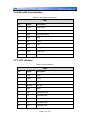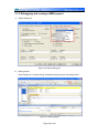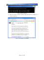
1
SBC1788 User Manual Release: 2012-08-06 SBC1788 User Manual Embest Technology Co., LTD Rev 1.0 SBC1788 Single Board Computer 120MHz LPC1788FBD208 NXP 32-bit ARM Cortex-M3 Microcontroller CPU Internal 512KB of Flash, 96KB of SRAM and 4KB of EEPROM Onboard 128MB Nand Flash, 32MB SDRAM USB2.0 Host Full-speed Port and 1 USB2.0 OTG Full-speed Port UARTs, RS485, Ethernet, CAN2.0B, LCD & Touchscreen, TF, Buzzer… Supports uC/OSⅡ_v2.86 & uC/GUI_v3.90a Supports FatFs_vR0.08a File System Supports LwIP_v1.4.0 Protocol Stack Page 1 of 129 COPYRIGHT SBC1788 is trademarks of Embest Technology Co., LTD. LPC1788 are trademarks of NXP. Microsoft, MS-DOS, Windows XP are trademarks of Microsoft Corporation. Important Notice Embest has ownership and rights to the use of this document. Information in the document is within the protection of copyright. Unless specifically allowed, any part of this Document should not be modified, issued or copied in any manner or form without prior written approval of Embest Technology Co., LTD. Page 2 of 129 Version of update records: Rev Date Description V1.0 2012-8-06 Initial version V1.1 2012-11-29 Removed “If 7 inch LCD be used, make sure that jumper JP1 is fitted.” in 4.1.1 LCD_Display,4.1.2 LCD_Touch,4.18 SSP,5.1 SBC1788-emWin512,and 5.3 SBC1788-uCOSII-uCGUI. Page 3 of 129 Contact: If you want to order products from Embest, please contact Marketing Department: Tel: +86-755-25635656 / 25636285 Fax: +86-755-25616057 E-mail: [email protected] If you want to get technical assistance from Embest, please contact Technical Assistance Department: Tel: +86-755-25503401 E-mail: [email protected] URL: http://www.armkits.com Address: Room 509, Luohu Science &Technology Building, #85 Taining Road, Shenzhen, Guangdong, China (518020) Page 4 of 129 Contents SBC1788 User Manual ........................................................................................................ 1 Charter 1 Overview ............................................................................................................ 10 1.1 Product introduction ............................................................................................. 10 1.2 Feature ................................................................................................................. 12 Charter 2 Hardware sysytem ............................................................................................. 15 2.1 Hardware Interface Diagram ................................................................................ 15 2.2 Hardware Interface ............................................................................................... 15 2.2.1 Power Input Jack........................................................................................ 15 2.2.2 Serial Port................................................................................................... 16 2.2.3 Ethernet Interface....................................................................................... 16 2.2.4 USB Host Connector .................................................................................. 17 2.2.5 USB Device Connector .............................................................................. 17 2.2.6 MicroSD Card Interface ............................................................................. 18 2.2.7 LCD Interface ............................................................................................. 18 2.2.8 JTAG Interface ........................................................................................... 20 2.2.9 PWM&SPI Interface ................................................................................... 21 2.2.10 UART&ADC/DAC Interface ...................................................................... 21 2.2.11 GPIO&I2C Interface ................................................................................. 22 2.2.12 CAN&485 Interface .................................................................................. 23 2.2.13 Key ........................................................................................................... 24 2.2.14 LED .......................................................................................................... 24 2.2.15 Jumper ..................................................................................................... 24 2.3 Hardware Dimension ............................................................................................ 25 Charter 3 Software Development ...................................................................................... 26 3.1 Keil MDK ............................................................................................................... 26 3.1.1 Building an existing MDK Project ............................................................... 26 3.1.2 Downloading program ................................................................................ 27 3.1.3 Debugging and running a MDK project...................................................... 29 Page 5 of 129 3.1.4 Creating a New MDK Project ..................................................................... 30 3.2 IAR EWARM ......................................................................................................... 34 3.2.1 Building an existing EWARM Project ......................................................... 34 3.2.2 Downloading and Debugging a EWARM project ....................................... 35 3.2.4 Creating a New EWARM Project ............................................................... 37 3.3 PC settings ........................................................................................................... 41 3.3.1 HyperTerminal connection ......................................................................... 41 3.3.2 PC network settings ................................................................................... 45 3.4 Flash magic .......................................................................................................... 48 Charter 4 Peripheral examples.......................................................................................... 52 4.1 LCD example ........................................................................................................ 53 4.1.1 LCD_Display .............................................................................................. 53 4.1.2 LCD_Touch................................................................................................. 55 4.2 USB-Device .......................................................................................................... 57 4.2.1 USB_MassStorage ..................................................................................... 57 4.2.2 USB_VirtualCom ........................................................................................ 58 4.3 USBHostLite ......................................................................................................... 62 4.4 Ethernet ................................................................................................................ 64 4.5 UART .................................................................................................................... 67 4.5.1 UART_Autobaud ........................................................................................ 67 4.5.2 UART_RS485............................................................................................. 69 4.6 EMC ...................................................................................................................... 71 4.6.1 Emc_NandFlashDemo ............................................................................... 71 4.6.2 Emc_SdramDemo ...................................................................................... 73 4.7 RTC ...................................................................................................................... 75 4.8 CAN ...................................................................................................................... 77 4.9 DMA ...................................................................................................................... 81 4.10 WDT.................................................................................................................... 83 4.11 TIMER ................................................................................................................. 86 Page 6 of 129 4.12 SYSTICK ............................................................................................................ 89 4.13 NVIC ................................................................................................................... 91 4.14 PWR ................................................................................................................... 93 4.15 GPIO ................................................................................................................... 95 4.16 PWM ................................................................................................................... 96 4.17 MCI ..................................................................................................................... 98 4.18 SSP................................................................................................................... 101 4.19 ADC .................................................................................................................. 103 4.20 DAC .................................................................................................................. 106 4.21 BOD .................................................................................................................. 108 4.22 CRC .................................................................................................................. 110 4.23 IAP .................................................................................................................... 113 Charter 5 Application Demonstration .............................................................................. 115 5.1 SBC1788-emWin512.......................................................................................... 115 5.2 SBC1788-Lwip-v1.4.0 ........................................................................................ 117 5.2.1 httpraw_sa ................................................................................................ 117 5.2.2 tcpecho_sa ............................................................................................... 119 5.3 SBC1788-uCOSII-uCGUI ................................................................................... 121 5.4 SBC1788-uCOS-II-v2.86 .................................................................................... 123 Charter 6 Various Other Tests Scenario .......................................................................... 124 6.1 LCD & Touch Screen .......................................................................................... 124 6.2 USB Device ........................................................................................................ 124 6.3 USB Host ............................................................................................................ 124 6.4 Ethernet .............................................................................................................. 124 6.5 UART .................................................................................................................. 124 6.6 RS485 ................................................................................................................. 124 6.7 NAND FLASH ..................................................................................................... 124 6.8 SDRAM ............................................................................................................... 124 6.9 RTC .................................................................................................................... 124 Page 7 of 129 6.10 CAN .................................................................................................................. 125 6.11 LED & Buzzer ................................................................................................... 125 6.12 MicroSD ............................................................................................................ 125 6.13 ADC .................................................................................................................. 125 6.14 DAC .................................................................................................................. 125 Charter 7 What’s in the BOX ........................................................................................... 126 Technical support & Warranty Service............................................................................. 127 Technical support service ......................................................................................... 127 Maintenance service clause ..................................................................................... 128 Basic notice to protect and maintenance LCD ......................................................... 129 Value Added Services............................................................................................... 129 Page 8 of 129 Charter 1 Overview 1.1 Product introduction Embest SBC1788 Single Board Computer is an compact industrial controller board based on NXP’s LPC1788FBD208 ARM Cortex-M3 microcontroller which is running on up to 120MHz with 512KB of internal Flash memory, 96KB of internal SRAM, 4KB of internal EEPROM, a 10/100 Ethernet Media Access Controller (MAC), a USB full speed device/host/OTG controller, four UARTs, two CAN channels and a collection of serial communications interfaces. The SBC1788 board also has external 128MB Nand Flash and 32MB SDRAM. It takes full features of the LPC1788 microcontroller and has exposed many hardware features through headers or connectors including UARTs, USB, Ethernet, CAN, LCD, I2C, SPI, PWM, ADC and DAC to meet various applications. Embest has ported uC/OS-II to support their Cortex-M3 SBC1788 board and the software also features the GUI support on uC/OS-II and LwIP_v1.4.0 protocol support. Embest provides the uC/OS-II BSP and plenty of software examples, board schematic and user manual to help customer better understanding this board and develop your own applications. Note: You are required to purchase a license for using uC/OS-II and uC/GUI in any commercial application Page 9 of 129 SBC1788 can be used in the following applications: Industrial Control Medical Equipment Home Automation Human Interface Consumer Electronics Test and Measurement SBC1788 Function Block Diagram LEGEND CPU internal module Onboard IC or reserved chip Onboard Interfaces or Connectors Page 10 of 129 1.2 Feature The LPC1788 is a Cortex-M3 microcontroller for embedded applications featuring a high level of integration and low power consumption at frequencies of 120 MHz Features include 512 KB of flash memory, 96 KB of data memory, Ethernet, USB 2.0 Host/OTG/ Device, 8-channel DMA controller, 5 UARTs, 2 CAN channels, 3 SSP/SPI, 3 I2C, I2S, 8-channel 12-bit ADC, 10-bit DAC, QEI, LCD controller, SD/MMC interface, motor control PWM, 4 general purpose timers, 6-output general purpose PWM, ultra-low power Real-Time Clock with separate battery supply, and up to 165 general purpose I/O pins. The SBC1788 Single Board Computer exposes many of these features to the user in support of developing specific solutions. This board is characterized as follows: Processor NXP LPC1788FBD208 Microcontroller ARM 32-bit Cortex-M3 CPU, frequency up to 120MHz On chip 512KBytes Flash,96KBytes SRAM,4KBytes EEPROM Flexible static memory controller that supports Compact Flash, SRAM, PSRAM, Nor and Nand memories LCD controller, supporting up to 24-bit true color mode and 1024*768 pixels resolution USB 2.0 FS Device/Host/OTG 10/100 Ethernet MAC with MII/RMII interface and associated DMA controller 2 CAN 2.0B interfaces, 5 USARTs and 1 I2S, 3 I2C and 3 SSP 4 x 32-bit timers, 2 x standard PWM and 1 motor control PWM with support for Three-phase motor control 1 x 12-bit A/D converter, 1 x 10-bit D/A converter Up to 165 general purpose I/O pins External Memory and Storage 128Mbytes Nand Flash 32Mbytes SDRAM 4MBytes SPI Flash and 2kBytes EEPROM (Reserved for soldering) Page 11 of 129 Micro SD card slot LCD/Touch Screen 4.3 inch (480 x 272-pixel RGB resolution) and 7 inch (800 x 480-pixel RGB resolution) TFT color LCDs for selections 4-wire resistive touch screen 16-bit RGB565 color format Data Transfer Interfaces 1-channel 3-wire RS232 Serial Port (UART0, DB9) 1-channel 5-wire Serial port, TTL voltage (UART1, RS232 is designable) 1-channel 3-wire RS232 Serial port (UART3, TTL is designable) 1-channel 3-wire Serial port, TTL voltage (UART4, RS232 is designable) 1-channel RS485 Serial port (brought out by Phoenix Connector) 1 x USB2.0 Host, Full-speed, 12Mbps 1 x USB2.0 OTG/Device/Host, Full-speed, 12Mbps 10/100 Ethernet interface 1 x CAN2.0B interface Input Interface and Other Facilities 2 x USER buttons 1 x RESET button 1 x ISP button 20-pin standard JTAG interface 1 x Buzzer RTC battery socket (User needs to prepare battery, CR1220 model is recommended) Windowed watchdog timer (WWDT) Supports onboard watchdog reset through hardware (reserved function) 1 x LED for Power indicator 1 x LED for USB Host FS indicator 1 x LED for USB OTG FS indicator Page 12 of 129 4 x User LEDs 3 x Extension Interfaces (2.54mm pitch 2*10-pin connector) Up to 18 independent GPIO pins are all brought out 5*5 matrix keypad interface channel general purpose PWM with 6 outputs One 3-channel ADC One DAC One SPI One I2C Mechanical Parameters Dimensions: 120 mm x 87 mm (6-layer PCB design) Power consumption: 120mA@12V (working without LCD) Working Temp.: -40 ℃ ~ 85 ℃ Humidity Range: 0% ~ 90 Page 13 of 129 Charter 2 Hardware sysytem 2.1 Hardware Interface Diagram The hardware interface diagram of SBC1788: 2.2 Hardware Interface 2.2.1 Power Input Jack Table 2-1 Power Input Jack J1 Pin Signal Description 1 +12V Power supply(+12V) 1.25A (Type) Page 14 of 129 2 GND GND 3 GND GND 2.2.2 Serial Port Table 2-2 Serial Port Interface COM1 Pin Signal Description 1 NC NC 2 RXD Receive data 3 TXD Transit data 4 NC NC 5 GND GND 6 NC NC 7 NC NC 8 NC NC 9 NC NC 2.2.3 Ethernet Interface Table 2-3 Ethernet Interface CON10 Pin Signal Description 1 TX+ TX+ output 2 TX- TX- output 3 RX+ RX+ input 4 CT CT 5 CT CT 6 RX- RX- input 7 NC NC 8 SHIELD Shield Page 15 of 129 9 LED1 LINK LED 10 VDD3V3 3.3V Power for LED 11 LED2 SPEED LED 12 VDD3V3 3.3V Power for LED 13 4&5 Connect to shield 14 7&8 Connect to shield 15 NC NC 16 NC NC 2.2.4 USB Host Connector Table 2-4 USB Host connector CON2 Pin Signal Description 1 VBUS +5V 2 D- USB Data- 3 D+ USB Data+ 4 GND GND 2.2.5 USB Device Connector Table 2-5 USB Device Connector CON1 Pin Signal Description 1 VBUS +5V 2 D- USB Data- 3 D+ USB Data+ 4 ID USB ID 5 GND GND Page 16 of 129 2.2.6 MicroSD Card Interface Table 2-6 MicroSD Card Interface CON3 Pin Signal Description 1 DAT2 Card data 2 2 DAT3 Card data 3 3 CMD Command Signal 4 VDD VDD 5 CLK Clock 6 VSS VSS 7 DAT0 Card data 0 8 DAT1 Card data 1 9 CD Card detect 2.2.7 LCD Interface Table 2-7 LCD Interface CON9 Pin Signal Description 1 GND GND 2 DCLK DCLK 3 HSYNC HSYNC 4 VSYNC VSYNC 5 GND GND 6 RST RST(Reserved) 7 R3 Red data input 8 R4 Red data input 9 R5 Red data input 10 R6 Red data input Page 17 of 129 11 R7 Red data input 12 GND GND 13 G2 Green data input 14 G3 Green data input 15 G4 Green data input 16 G5 Green data input 17 G6 Green data input 18 G7 Green data input 19 GND GND 20 GPIO_0 GPIO(Reserved) 21 B3 Blue data input 22 B4 Blue data input 23 B5 Blue data input 24 B6 Blue data input 25 B7 Blue data input 26 GND GND 27 DEN Display enable 28 VDD3V3 +3.3V power supply 29 VDD3V3 +3.3V power supply 30 GPIO_1 I2C_SCL(Reserved) 31 GPIO_2 I2C_SDA(Reserved) 32 Y+ Terminal of touch panel 33 X- Terminal of touch panel 34 Y- Terminal of touch panel 35 X+ Terminal of touch panel 36 PWREN LCD power enable 37 VDD5V +5V power supply 38 PWM LED Dimming Control by PWM Signal 39 VDD5V +5V power supply Page 18 of 129 40 VDD12V +12V power supply 2.2.8 JTAG Interface Table 2-8 JTAG Interface CON5 Pin Signal Description 1 VTREF +3.3V power supply 2 VSUPPLY +3.3V power supply 3 NTRST Test system reset 4 GND GND 5 TDI Test data input 6 GND GND 7 TMS Test mode select 8 GND GND 9 TCK Test clock 10 GND GND 11 RTCK GND 12 GND GND 13 TDO Test data output 14 GND GND 15 NSRST Test system reset 16 GND GND 17 DBGRQ Connect to GND 18 GND GND 19 DBGACK Connect to GND 20 GND GND Note: Connect JTAG tool (ULink, JLink etc.) to SBC1788 JTAG interface CON5 through IDC20 cable. Red line onside indicates the first pin of IDC20 cable. Triangle onside indicates the first pin of JTAG interface. Page 19 of 129 2.2.9 PWM&SPI Interface Table 2-9 PWM & SPI Interface CON6 Pin Signal Description 1 VDD3V3 +3.3V power supply 2 GND GND 3 P3_19 P3[19] 4 PWM1_1 PWM1[1] 5 P3_20 P3[20] 6 PWM1_2 PWM1[2] 7 P3_21 P3[21] 8 PWM1_3 PWM1[3] 9 P3_22 P3[22] 10 PWM1_4 PWM1[4] 11 P3_23 P3[23] 12 PWM1_5 PWM1[5] 13 GND GND 14 PWM1_6 PWM1[6] 15 SPI0_SCK SPI0_SCK 16 SPI0_SSEL SPI0_SSEL 17 SPI0_MOSI SPI0_MOSI 18 SPI0_MISO SPI0_MISO 19 GND GND 20 VDD5V +5V power supply 2.2.10 UART&ADC/DAC Interface Page 20 of 129 Table 2-10 UART&ADC/DAC Interface CON7 Pin Signal Description 1 VDD3V3 +3.3V power supply 2 GND GND 3 ADC0_IN0 ADC0_IN0 4 ADC0_IN2 ADC0_IN2 5 ADC0_IN1 ADC0_IN0 6 DAC_OUT DAC_OUT 7 P1_05 P1[5] 8 GND GND 9 TXD3 UART3_ TXD 10 TXD1 UART1_ TXD 11 RXD3 UART3_ RXD 12 RXD1 UART1_ RXD 13 P1_13 P1[13] 14 P0_14 P0[14] 15 TXD4 UART4_ TXD 16 CTS1 UART1_CTS1 17 RXD4 UART4_ RXD 18 RTS1 UART1_RTS1 19 GND GND 20 VDD5V +5V power supply 2.2.11 GPIO&I2C Interface Table 2-11 GPIO&I2C Interface CON6 Pin Signal Description 1 VDD3V3 +3.3V power supply Page 21 of 129 2 GND GND 3 VDD3V3 +3.3V power supply 4 GND GND 5 P4_21 P4[21] 6 I2C2_SCL I2C2_SCL 7 P4_22 P4[22] 8 I2C2_SDA I2C2_SDA 9 P4_23 P4[23] 10 P0_04 P0[04] 11 P4_26 P4[26] 12 P0_05 P0[05] 13 P4_27 P4[27] 14 P0_18 P0[18] 15 P4_28 P4[28] 16 P2_25 P2[25] 17 GND GND 18 VDD5V +5V power supply 19 GND GND 20 VDD5V +5V power supply 2.2.12 CAN&485 Interface Table 2-12 CAN&485 Interface J1 Pin Signal Description 1 +12V Power supply(+12V) 1.25A (Type) 2 GND_IN GND for Input +12V 3 CAN1H CAN1 H 4 CAN1_L CAN1 L 5 485A RS485 A Page 22 of 129 6 485B RS485 B 2.2.13 Key Table 2-13 KEY S1 & SW1~SW2 Pin Signal Description S1 RESET System reset key SW1 USER1 User-defined key 1 SW2 USER2 User-defined key 2 SW3 ISP ISP Function key 2.2.14 LED Table 2-14 LEDs LED 1~4 Pin Signal Description LED 1 P4[15] User-defined LED 1 LED 2 P4[16] User-defined LED 2 LED 3 P4[17] User-defined LED 3 LED 4 P4[18] User-defined LED 4 2.2.15 Jumper Table 2-15 Jumper JP1 Jumper State Description ON Power 描述 3.3V to LCD OFF Don’t power 3.3V to LCD (default) JP1 Page 23 of 129 2.3 Hardware Dimension The hardware dimension of SBC1788 (Unit: mm): Top Layer Component HeightMAX = 13 mm Bottom Layer Component HeightMAX = 3 mm Board Thick =1.6mm Page 24 of 129 Charter 3 Software Development There are mainly two software development environments for LPC177x8x series MCU, Keil MDK-ARM and IAR EWARM. The following sections will give a short description of these softwares and show how to use them. 3.1 Keil MDK The LPC177x_8x series MCUs require MDK4.20 and newer versions. All MDK projects under folder \MDK-ARM in the CD-ROM are built with MDK4.22a. The sections give a short description of how to use the Keil MDK to develop application software. For more detail, please reference at the related documentation. 3.1.1 Building an existing MDK Project 1) Open a project. Open MDK-ARM μVision4 -> File -> Open and select a project to open. Figure 3-1 Open a MDK project 2) Rebuild the project. Click “Rebuild” to build or rebuild the project. If the project is successfully compiled, the following window is displayed as the figure shown below. Page 25 of 129 Figure 3-2 Rebuild the project 3.1.2 Downloading program 1) Select your download tool. Select Target Options->Utilities and select your driver for you download tool. Figure 3-3 Select your download tool 2) Select Flash programming algorithm. Page 26 of 129 Figure 3-4 Select Flash programming algorithm 3) Download program. Click Load icon or select Flash->Download to download program into flash. Figure 3-5 Download program Page 27 of 129 3.1.3 Debugging and running a MDK project 1) Select debug tool Figure 3-6 Select debug tool 2) Debug project. Click Debug icon or select Debug->Start/Stop debug session into debug mode. Figure 3-7 Debug project Page 28 of 129 3.1.4 Creating a New MDK Project 1) Create a new project. Open MDK µVision4 then Click Project->New uVision Project. Save the project. Figure 3-8 Select debug tool 2) Select CPU for new project. Figure 3-9 Select CPU for new project 3) A dialogue box pops up to ask if you want to add Startup code to project. You can select “Yes”, uVision will add it for you, or “No” then you need to add it by yourself. The source file of Startup code is located in the folder: \core\Device\NXP\LPC177x_8x\Source\Templates\ARM Page 29 of 129 Figure 3-10 Add Start code 4) Now add file groups to project. Right click on “Target”, select “Add Group…” and name the file group. Figure 3-11 Now add file group 5) Add files to group. Right click on group name and seclect Add Files to Group… In order to organize the source files in an order, please add files to the related group. Page 30 of 129 Figure 3-12 Add files to group 6) Setup Target options. Click the icon “Target Options”.Select ‘C/C++’ tab to and add Include files path. Figure 3-13 Add include file path 7) Rebuild the project. Please reference at 3.1.1 Building an existing MDK Project. 8) Download the program. Page 31 of 129 Please reference at 3.1.2 Downloading program. 9) Debug the project. Please reference at 3.1.3 Debugging and running a MDK project. Page 32 of 129 3.2 IAR EWARM The LPC177x_8x series MCUs require IAR EWARM 6.20 and later versions. All IAR projects under folder \EWARM in the CD-ROM are built with IAR EWARM 6.30. User can download the evaluation edition for free from www.iar.com. The sections 3.2.1 Building an existing EWARM Project and 3.2.4 Creating a New EWARM Project give a short description of how to use the IAR EWARM to develop application software. For more detail, please reference at the related documentation. 3.2.1 Building an existing EWARM Project 1) Open a project. Open IAR Embedded Workbench and select File -> Open to open a project. Figure 3-14 Open a project 2) Rebuild the project. Click icon Make or select Project-> Make / Rebuild All to rebuild the project. Page 33 of 129 Figure 3-15 Rebuild the project 3.2.2 Downloading and Debugging a EWARM project 1) Select debug and download tool. Right click on project name in workspace, select Project -> Options -> Debugger and select driver for debug and download tool. Figure 3-16 Select debug and download tool Page 34 of 129 2) Select Verify download. Select Debug->Download tab, and then select Verify download. Figure 3-17 Select Verify download 3) Download and debug the project Click on Download and debug icon into debug mode. Figure 3-18 Download program Debug interface display like this: Page 35 of 129 Figure 3-19 Debug interface 3.2.4 Creating a New EWARM Project 1) Create a new project. Open IAR EWARM then Click Project->Create new project. A dialogue box pops up to ask what kind of project template you want to create. Please select Empty Project and save the project. Figure 3-20 Create a new project Page 36 of 129 2) Add Files Group. Right click on project name in workspace, select Add->Add Group. Figure 3-21 Add group 3) Add source file. Right click on project name in workspace, select Add->Add file. Figure 3-22 Add source file 4) Select CPU for new project. Right click on project name in workspace, select Options->General options->Target. Page 37 of 129 Then select NXP LPC1788 for project. Figure 3-23 Select CPU for new project 5) Setup Target options. Select C/C++ Compiler->Preprocessor tab, then add include file path in Additional include directories. Figure 3-24 Setup Target options 6) Add path of icf (linker configuration file) as shown below: Page 38 of 129 \code\LPC177x_8x_StdPeriph_Demo\makesection\makerule\linker Figure 3-25 Add path of icf file 7) Build the project Please reference at 3.2.1 Building an existing EWARM Project. 8) Download and debug the project Please reference at 3.2.2 Downloading and Debugging a EWARM project. Page 39 of 129 3.3 PC settings In order to run and test Ethernet and other examples that need print massage via HyperTerminal, PC should do some settings, HyperTerminal connection and network settings.All the settings shown in this article are based on Windows XP OS. 3.3.1 HyperTerminal connection 1) Select Start -> All Programs -> Accessories -> Communication -> Hyper Terminal. Find the HyperTerminal, as shown below: Figure 3-26 Create a new HyperTerminal 2) Create a new HyperTerminal connection, enter a name and choose an icon. Page 40 of 129 Figure 3-27 Description for new connection 3) Select the specific serial port from the list as per your computer COM port configuration: Figure 3-28 Select a COM port for connection 4) Set parameters for serial port connection as follows: Page 41 of 129 Figure 3-29 Settings for the selected port 5) A Hyper Terminal connection with PC serial port have been established as shown below: Page 42 of 129 Figure 3-30 Hyper Terminal successfully built Page 43 of 129 3.3.2 PC network settings In order to test Ethernet examples, please set up the PC network environment. Make sure that the PC's IP address and the MB407 board's IP address are on the same network. 1) On PC, select Start-> Control Panel-> Network connections-> Local Area Connection-> Properties, as shown below: Figure 3-31 Local Area Connection 2) Click ‘Properties’, this will open the window of Local Area Connection Properties, as shown below: Figure 3-32 Local Area Connection Properties Page 44 of 129 3) Double click ‘TCP / IP Options’, opens a window for TCP / IP Properties, as shown below: Figure 3-33 TCP / IP Options 4) Click the ‘Advanced’ option, open a window for “Advanced TCP / IP settings”, as shown below: Figure 3-34 Advanced TCP / IP settings 5) Click the ‘Add’ option; open a window for "Add TCP / IP". Enter the IP address (must not be 192.168.0.100, because it is default IP address for SBC1788) and subnet mask, then click "Add”, as shown below: Page 45 of 129 Figure 3-35 Add TCP/IP address 6) Click “OK” to finish network setup. Figure 3-36 TCP/IP address successfully setup Page 46 of 129 3.4 Flash magic LPC1788 supports ISP over UART for program download. ISP is short for In-System Programming. The LPC1788 contains a bootloader in ROM that can be enabled by pulling pin P2.10 low during reset. The application can then be downloaded over UART#0 (serial channel). In order to run ISP, please follow steps as below: 1) Connect a null-modem female/female RS232 cable between the DB9 connector COM1 (USART0) and PC serial port. 2) Plug in +12V power supply. 3) Create HEX file with MDK-ARM. Open MDK-ARM project, configure Target Option and select Create HEX file. Rebuild the Project, generate HEX file. The hex file is located in \Keil\Flash subfolder of the project directory. Figure 3-37 Configure MDK output option 4) Create HEX file with IAR EWARM. Open EWARM project, configure Options and select output format. Select Intel extended for output .Rebuild the Project, generate hex file. Page 47 of 129 The hex file is located in \EWARM\Flash\Exe subfolder of the project directory. Figure 3-38 Configure EWARM output option 5) Install Flash Magic software. The software is located in the folder of \Flash Magic. 6) Open Flash magic software, and then select Options->Advanced Options. Figure 3-39 Flash Magic Advance Options Page 48 of 129 7) Then select the Hardware Config tab end set checkboxes and T1/T2 numbers according to figure below. Figure 3-40 Flash Magic Hardware Config 8) Flash magic settings. Figure 3-41 Flash Magic settings Page 49 of 129 Communications Select Device: LPC1788 COM Port: According to your PC serial port Baud Rate: Shall be set to 57600 or lower Interface: None (ISP) Oscillator (MHz): Shall be set to 12.000 Hex File Select the hex/binary file to be downloaded. 9) Download hex file ISP (SW3) button maintained pressed. Press RESET button and cilk Start icon to start downloading the hex file. After download finish, release ISP (SW3) button. Press RESET button. After reset, the MCU start to run. Page 50 of 129 Charter 4 Peripheral examples Embest provides plenty of peripheral examples. All the peripheral examples are based on the peripheral driver library. The structure of peripherals examples is shown in figure below. Figure 4-1 Peripherals examples structure Description of \code\LPC177x_8x_StdPeriph_Demo folder 1) BoardSupport subfolder This folder contains source of SDRAM, Nand Flash, LCD and Phylan drivers. 2) Core subfolder This folder contains the CMSIS files and startcode for Keil and IAR. 3) Drivers subfolder This subfolder contains sources of LPC1788 peripheral drivers. Each peripheral has a source code file, lpc177x_8x_ppp.c, and a header file, lpc177x_8x_ppp.h. 4) Examples subfolder This subfolder contains a set of examples for some peripherals with preconfigured projects for EWARM, MDK-ARM toolchains. The sections in this charter give a description of some peripheral examples. User can learn about the feature of LPC1788 peripherals and how to use them by reading these sections. Some examples may require additional hardware such as an oscilloscope. For further information on the required hardware, please reference at the Readme file provided within each example folder. Page 51 of 129 4.1 LCD example The LCD folder contains two examples: LCD_Display LCD_Touch 4.1.1 LCD_Display 1. Purpose LCD_Touch example describes how to test touch screen and do calibration on SBC1788. 2. Description In this example, four points on the corner of touch screen need to be touch to complete calibration. 3. Hardware configuration SBC1788 supports two kinds of LCD & Touch Screen module: LCD6000-43T, 4.3 inch, resolution: 480*272 LCD6000-70T, 7 inch, resolution: 800*480 Mount LCD module onto SBC1788 CON9 through LCD cable. Red line onside indicates the first pin of LCD cable. Triangle onside indicates the first pin of LCD connector. Note: Make sure that LCD module mount onto SBC1788 correctly. 4. Software configuration Do the change in the file lcd_driver.h according to LCD module: If 4.3 inch LCD module be used: Page 52 of 129 Figure 4-2 Change macro for 4.3 inch LCD module If 7 inch LCD module be used Figure 4-3 Change macro for 7 inch LCD module 5. Steps to run 1) Mount LCD module onto SBC1788 CON9 through LCD cable. 2) Plug in +12V adaptor and power the board. 3) Rebuild the example, and then download the program into SBC1788 Flash. 4) Reset SBC1788 and run the example on the board. 5) Testing actions and results: The LCD displays 4 color bars, red, green, blue and yellow. A blue cursor moves from one side to another side on the red bar. Page 53 of 129 4.1.2 LCD_Touch 1. Purpose LCD_Touch example describes how to test LCD module on SBC1788. 2. Description The LCD displays 4 color bars, red, green, blue and yellow. A blue cursor moves from one side to another side on the red bar. 3. Hardware configuration SBC1788 supports two kinds of LCD module: LCD6000-43T, 4.3 inch, resolution: 480*272 LCD6000-70T, 7 inch, resolution: 800*480 Mount LCD module onto SBC1788 CON9 through LCD cable. Red line onside indicates the first pin of LCD cable. Triangle onside indicates the first pin of LCD connector. Note1: Make sure that LCD module mount onto SBC1788 correctly. If 4.3 inch LCD be used, please remove C3, C5, C6 and C7 from the board. C3, C5, C6 and C7 are designed for improving EMC performance, while they may degrade touch screen performance. 4. Software configuration Do the change in the file lcd_driver.h according to LCD module: If 4.3 inch LCD module be used: Page 54 of 129 Figure 4-4 Change macro for 4.3 inch LCD module If 7 inch LCD module be used Figure 4-5 Change macro for 7 inch LCD module 5. Steps to run 1) Mount LCD module onto SBC1788 CON9 through LCD cable. 2) Plug in +12V adaptor and power the board. 3) Rebuild the example, and then download the program into SBC1788 Flash. 4) Reset SBC1788 and run the example on the board. 5) Testing actions and results: Click calibration points accurately using a touch pen. LCD will give massage whether calibration is OK. If calibration is OK, then MCU will enter into Calibration_Test_Dispose function. In this function LCD will display the value of points touched by the pen. Both ADC values and coordinate values are displayed. Page 55 of 129 4.2 USB-Device The USB folder contains two examples: USB_MassStorage USB_VirtualCom 4.2.1 USB_MassStorage 1. Purpose This example describes how to write a simple USB Mass Storage application on LPC177x_8x. 2. Description The MassStorage project is a Mass Storage simple demo run on LPC177x_8x. It demonstrates an USB Memory based on USB Mass Storage Class. The USB Memory is automatically recognized by the host PC running Windows which will load a generic Mass Storage driver. 3. Software configuration HyperTerminal is used in this example. Please reference at 3.3.1 HyperTerminal connection for more details. 4. Steps to run 1) Connect SBC1788 to a PC with a 'USB type A to Mini-B' cable through USB connector CON1. 2) Connect SBC1788 to PC serial port with a null-modem female/female RS232 cable through the DB9 connector COM1 (USART0). 3) Plug in +12V adaptor and power the board. 4) Rebuild the example, and then download the program into SBC1788 Flash. 5) Reset SBC1788 and run the example on the board. 6) Testing actions and results: Page 56 of 129 After reset, see UGL (USB Good Link), then open “My Computer” on PC to check “LPC177x_8x” disk drive.LED6 turn on. Open the disk, “Readme.txt” file will shown with read-only attribute. Figure 4-6 Readme.txt file in LPC178x disk Try handling data inside (as create, copy, delete...)->They are all ok. 4.2.2 USB_VirtualCom 1. Purpose This example describes how to configure USB Device of as a virtual COM port. 2. Description The PC will install a virtual COM port on the PC (see Driver Installation). After installation an additional port "LPC177x_8x USB VCom Port(COMx)" can be found under System/Hardware/Device Manager/Ports(COM&LPT). Number "x" is not fixed as different PC configuration may have different "x" displayed on the device manager. The USB host driver assigns "x" dynamically based on the existing COM port configuration of the system. To test the virtual COM Port that just linked, it should: Page 57 of 129 Use one more standard UART connection between the board and the PC Checking if data transmitting from PC through standard COM to the board then back to PC through virtual COM is correct or not And oppositely checking if data transmitting from PC through virtual COM to the board then back to PC through standard COM is correct or not The data can be monitored by 2 separate serial terminal programs. Notes: To use standard UART Port on the board, it should consider #define PORT_NUM in serial.h for the UART number will be use directly with PC. 3. Driver Installation "Welcome to the Found New Hardware Wizard" appears select 'No, not this time' press 'Next' select 'Install from a list or specific location (Advanced)' press 'Next' select 'Search for the best driver in these locations' check 'include this location in the search' set to <project folder> press 'Next' Note: The driver, lpc17x_8x-vcom.inf or lpc17xx-vcom.inf, is located in the project folder. "Hardware Installation Guidance" appears select the driver and press 'Next' Note: In this step, if there is any requirement about "usbser.sys", please download the file from the Ethernet. "Completing the Found New Hardware Wizard" appears press 'Finish' Page 58 of 129 4. Software configuration HyperTerminal is used in this example. Please reference at 3.3.1 HyperTerminal connection for more details. 5. Steps to run 1) Connect SBC1788 to a PC with a 'USB type A to Mini-B' cable through USB connector CON1. LED6 turn on. 2) Connect SBC1788 to PC serial port with a null-modem female/female RS232 cable through the DB9 connector COM1 (USART0). 3) Plug in +12V adaptor and power the board. 4) Rebuild the example, and then download the program into SBC1788 Flash. 5) Reset SBC1788 and run the example on the board (install driver if required). 6) Testing actions and results: If UGL (USB Good Link) LED on the board is turned ON, open “Device Manager > Ports (COM & LPT)” to check for the appearance of “LPC178x USB VCOM Port (COMx)” device. Figure 4-7 LPC178x USB VCOM Port Open one HyperTerminal for COM3 and other for COMx with configuration in Page 59 of 129 Section 3.3.1 HyperTerminal connection. Type any character on one HyperTerminal screen and see this character will be echoed in other screen and vice versa. Figure 4-8 Communication between Standard COM and USB virtual COM Page 60 of 129 4.3 USBHostLite 1. Purpose This example describes how to write a simple USB Host Controller on LPC177x_8x. 2. Description This sample demonstrates how to access the files on "USB Flash drive" connected to USB Host port on evaluation board using NXP Semiconductors LPC177x_8x MCU. When a USB Mass Storage device is connected, it enumerates the device, mounts the file system on "USB Flash drive" and then executes a file copy. 3. Hardware configuration A U disk is needed in this example. Kingston 1GB/2GB or SanDisk 2GB U Disk is recommended. 4. Software configuration HyperTerminal is used in this example. Please reference at 3.3.1 HyperTerminal connection for more details. 5. Steps to run 1) Copy FILENAME_R.txt and Folder1 in the project folder to U Disk. 2) Insert U Disk into SBC1788 CON2. 3) Connect SBC1788 to PC serial port with a null-modem female/female RS232 cable through the DB9 connector COM1 (USART0). 4) Plug in +12V adaptor and power the board. 5) Rebuild the example, and then download the program into SBC1788 Flash. 6) Reset SBC1788 and run the example on the board (install driver if required). 7) Testing actions and results: The content on serial terminal should be like this: ******************************************************************************** Page 61 of 129 Hello NXP Semiconductors UART Host Lite example - MCU: LPC177x_8x - Core: ARM CORTEX-M3 - UART Communication: 115200 bps This example used to test USB Host function. ******************************************************************************** Host Initialized Connect a Mass Storage device Mass Storage device connected Copying file... Copy completed Remove U disk from SBC1788 and then insert into PC. A FILENAME_W.txt is created in Folder1 and the content of the FILENAME_R.txt have been copy to FILENAME_W.txt. Page 62 of 129 4.4 Ethernet The Ethernet folder contains three examples: Emac_EasyWeb Emac_Raw Emac_uIP Emac_EasyWeb example describes how to implement an simple web application. Emac_Raw example describes how to test EMAC driver with raw packet frame format that is not related with any upper-layer (i.e. TCP/IP...). Emac_uIP example describes how to handle a single network interface and contains the IP, ICMP, UDP and TCP protocols. Emac_EasyWeb 1. Description This tiny web server was taken from the 'Design & Elektronik' extra issue 'Embedded Internet'. It can be downloaded from the following web site: www.elektroniknet.de/extraheft. The web page shows the values of two analog inputs (AN0 and AN1). This tiny webserver needs very little resources and therefore has some restrictions: only one active TCP session at any one time no support for fragmented IP datagrams no buffer for TCP datagrams received in wrong order only one web page. No GIF/JPG graphics possible. The IP address can be modified in the module tcpip.h to fit into your existing LAN (see MYIP_x). The default IP address is: 192.168.0.100 2. Hardware configuration Try to make an external 10K, 3 pins vary-resistor, 1 terminal connects to 3.3V or Page 63 of 129 VREFP, the other connects to GND, and the rest (middle pin) connects to ADC0_IN2 (P0.25, CON7.4). 3. Software configuration HyperTerminal and Ethernet are used in this example. Please reference at 3.3.1 HyperTerminal connection and 3.3.2 PC network settings for more details. 4. Steps to run 1) Connect the external 10K, 3 pins vary-resistor following the above instructions. 2) Connect the SBC1788 to a PC with a crossover Ethernet cable through RJ45 connector CON10. 3) Connect SBC1788 to PC serial port with a null-modem female/female RS232 cable through the DB9 connector COM1 (USART0). 4) Plug in +12V adaptor and power the board. 5) Rebuild the example, and then download the program into SBC1788 Flash. 6) Reset SBC1788 and run the example on the board (install driver if required). 7) Testing actions and results: After the evaluation board initialization, open command prompt on window PC and execute “ping 192.168.0.100” command. Figure 4-9 ‘ping’ command Open web browser, access to address "http://192.168.0.100" to display the content of webserver: Page 64 of 129 Figure 4-10 The content of the Emac_EasyWeb Turn potentiometer and see the update ADC value on this web. Figure 4-11 The content change after turning potentiometer Page 65 of 129 4.5 UART The UART folder contains six examples: UART_Autobaud UART_Dma UART_Interrupt UART_Polling Uart_Rs485Master Uart_Rs485Slave UART_Autobaud example is a simple UART example using auto baudrate mode. UART_Dma, UART_Interrupt, UART_Polling example scribes how to use UART in DMA, interrupt, polling polling mode Uart_Rs485Master and Uart_Rs485Slave example describes how to use RS485 functionality on UART2 of LPC1788 in master mode and slave mode. 4.5.1 UART_Autobaud 1. Description UART is configured as the default settings: Baudrate set to auto mode 8 data bit 1 Stop bit None parity After reset, firstly, type 'A' or 'a' character to start Auto baud rate mode. Once Auto baud rate mode completed, print welcome screen, then press any key to have it read in from the terminal and returned back to the terminal. 2. Software configuration HyperTerminal is used in this example. Please reference at 3.3.1 HyperTerminal connection for more details. Page 66 of 129 3. Steps to run 1) Connect SBC1788 to PC serial port with a null-modem female/female RS232 cable through the DB9 connector COM1 (USART0). 2) Plug in +12V adaptor and power the board. 3) Rebuild the example, and then download the program into SBC1788 Flash. 4) Reset SBC1788 and run the example on the board. 5) Testing actions and results: Press ‘A’ or ‘a’ character on the PC terminal to send back to the board. After receiving the above character, the IC will print the welcome screen on PC terminal. If typing any character on PC terminal, this character will be echo The content on serial terminal should be like this: AutoBaudrate Status: Synchronous! ******************************************************************************** Hello NXP Semiconductors UART Auto-Baudrate example - MCU: LPC177x_8x - Core: ARM CORTEX-M3 - UART Communication: 115200 bps This example used to test UART component with autobaudrate function. It will adjust its rate to synchronize with the sending data + Please press any key to be echoed + Press 'r' to re-show the welcome string + Press ESC to terminate ******************************************************************************** a Hello!Rr ******************************************************************************** Hello NXP Semiconductors UART Auto-Baudrate example Page 67 of 129 - MCU: LPC177x_8x - Core: ARM CORTEX-M3 - UART Communication: 115200 bps This example used to test UART component with autobaudrate function. It will adjust its rate to synchronize with the sending data + Please press any key to be echoed + Press 'r' to re-show the welcome string + Press ESC to terminate ******************************************************************************** UART Auto-Baudrate demo terminated! 4.5.2 UART_RS485 1. Description RS485 function on UART2 acts as Master mode on RS485 bus. Master device will send a specified slave device address value first, then master device will send data frames. After sending completed, master device wait for response from slave device (example RS485_slave). 2. Hardware configuration This example need two SBC1788 boards and do connection as follow: Figure 4-12 RS485 connection 3. Software configuration HyperTerminal is used in this example. Please reference at 3.3.1 HyperTerminal connection for more details. Page 68 of 129 Download Uart_Rs485Master program into SBC1788 #1(RS485 Master), Uart_Rs485Slave program into SBC1788 #2(RS485 Slave). 4. Steps to run 1) Connect SBC1788 #1(RS485 Master) to SBC1788 #2(RS485 Slave) through CON4 following above instructions. 2) Connect SBC1788 #1(RS485 Master) to PC serial port with a null-modem female/female RS232 cable through the DB9 connector COM1 (USART0). 3) Plug in +12V adaptor and power the two SBC1788 boards. 4) Rebuild the two examples, and then download the program into SBC1788 boards following above instructions. 5) Reset the two boards. After reset, the two boards run. 6) Testing actions and results: After reset, then see the serial terminal, it should be like this: Hello NXP Semiconductors RS485 demo in Master mode Sending to A... Receive: ACK Sending to B... Receive: No Dev Reply …… Sending to A... Receive: ACK Sending to B... Receive: No Dev Reply Page 69 of 129 4.6 EMC The EMC folder contains two examples: Emc_NandFlashDemo Emc_SdramDemo Emc_NandFlashDemo example describe how to use EMC connects with On-board NAND FLASH on SBC1788. Emc_SdramDemo example describes how to use EMC connects with On-board SDRAM on SBC1788. 4.6.1 Emc_NandFlashDemo 1. Description NAND flash use this case is Samsung K9F1G08U0B (or K9F1G08U0D). NAND flash memory range will be mounted at address: 0x8000 0000 - 0x800FF FFFF. First, EMC will be initialized and set up timer compatible with this NAND flash chip. Then check Device ID. If not correct, process will be entering into infinite loop and display error via UART. If ID device checking is ok, entire Flash memory will be erased, 2K block data will be written and read back for verify. Verify process result will be display on terminal screen. 2. Software configuration HyperTerminal is used in this example. Please reference at 3.3.1 HyperTerminal connection for more details. 3. Steps to run 1) Connect SBC1788 to PC serial port with a null-modem female/female RS232 cable through the DB9 connector COM1 (USART0). Page 70 of 129 2) Plug in +12V adaptor and power the board. 3) Rebuild the example, and then download the program into SBC1788 Flash. 4) Reset SBC1788 and run the example on the board. 5) Testing actions and results: After reset, then see the serial terminal, it should be like this: ******************************************************************************** Hello NXP Semiconductors # NANDFLASH K9F1G08U0B testing - MCU: LPC177x_8x - Core: Cortex-M3 - UART Comunication: 115200 bps Write and verify data with on-board NAND FLASH ******************************************************************************** Init NAND Flash... Read NAND Flash ID: ECF19500 Checking valid block... Erase entire NAND Flash... Write a block of 2K data to NAND Flash... Read back a block of 2K data from NAND Flash... Verify data... Verifying complete! Testing terminated! Page 71 of 129 4.6.2 Emc_SdramDemo 1. Description NOR flash use this case is 256Mbit SDRAM Micron MT48LC8M16A2P_75IT. NOR flash memory range will be mounted at address: 0xA000 0000 - 0xAFFF FFFF. First, EMC will be initialized and set up timer compatible with this SDRAM chip.Entire SDRAM will be cleared. Then continue write data into SDRAM in 8-bits mode and 16-bits mode sequentially. After each mode writing, data in sdram will be verify. If verify process fail, program will enter into infinite loop. Please observe terminal screen for more information. 2. Software configuration HyperTerminal is used in this example. Please reference at 3.3.1 HyperTerminal connection for more details. 3. Steps to run 1) Connect SBC1788 to PC serial port with a null-modem female/female RS232 cable through the DB9 connector COM1 (USART0). 2) Plug in +12V adaptor and power the board. 3) Rebuild the example, and then download the program into SBC1788 Flash. 4) Reset SBC1788 and run the example on the board. 5) Testing actions and results: After reset, then see the serial terminal, it should be like this: ******************************************************************************** Hello NXP Semiconductors Test SDRAM mt48lc16m16A2P with LPC1788 EMC - MCU: LPC177x_8x - Core: Cortex-M3 Page 72 of 129 - UART Comunication: 115200 kbps Write and verify data with on-board SDRAM ******************************************************************************** Init SDRAM... Clear content of SDRAM... Writing in 8 bits format... Verifying data... Continue writing in 16 bits format... Clear content of SRAM... Writing in 16 bits format... Verifying complete, testing terminated! Page 73 of 129 4.7 RTC The RTC folder contains three examples: Rtc_Alarm Rtc_Calendar Rtc_Calibration Rtc_Alarm example describes how to generate interrupt in Second Counter Increment Interrupt (1s) and generate Alarm interrupt at 10s. Rtc_Calendar example describes how to configure RTC calendar. Rtc_Calibration example describes how to calibrate real-time clock. Rtc_Calendar 1. Description As an application example, it demonstrates how to setup the RTC peripheral and to be used to keep time. 2. Hardware configuration A button cell battery is needed and type model CR1220 is recommended. Install the battery into SBC1788 BAT1. 3. Software configuration HyperTerminal is used in this example. Please reference at 3.3.1 HyperTerminal connection for more details. 4. Steps to run 1) Install the button cell battery into SBC1788 BAT1. 2) Connect SBC1788 to PC serial port with a null-modem female/female RS232 cable through the DB9 connector COM1 (USART0). 3) Plug in +12V adaptor and power the board. 4) Rebuild the example, and then download the program into SBC1788 Flash. 5) Reset SBC1788 and run the example on the board. Page 74 of 129 6) Testing actions and results: After reset, then see the serial terminal, it should be like this: Restart the SBC1788 board, RTC calendar keeps the time. ******************************************************************************** Hello NXP Semiconductors RTC Set Example: - MCU: LPC177x_8x - Core: ARM CORTEX-M3 - UART Communication: 115200 bps A simple RTC Calendar example. To generate interrupt in Second Counter Increment Interrupt (1s) ******************************************************************************** Current time set to: 02012/003/013 016:015:030 02012/003/013 016:015:031 02012/003/013 016:015:032 02012/003/013 016:015:033 ******************************************************************************** Hello NXP Semiconductors RTC Set Example: - MCU: LPC177x_8x - Core: ARM CORTEX-M3 - UART Communication: 115200 bps A simple RTC Calendar example. To generate interrupt in Second Counter Increment Interrupt (1s) ******************************************************************************** Current time is availability 02012/003/013 016:015:034 02012/003/013 016:015:035 Page 75 of 129 02012/003/013 016:015:036 02012/003/013 016:015:037 02012/003/013 016:015:038 4.8 CAN The CAN folder contains two examples: Can_Aflut Can_Selftest Can_Aflut example describes how to use CAN driver functions for setup and change AFLUT table dynamically. Can_Selftest example describes how to test CAN self-test mode. Can_Aflut 1. Description Using 2 pcs SBC1788 baord to test CAN operation. This example supports all kind of identifier: FullCAN, explicit or group format. The CANs are set baudrate at 125KHz. First, settup AF look-up table with 5 sections: 6 entries for FullCAN section 6 entries for Standard Frame Format (SFF) section 6 entries for Group Standard Frame Format (SFF_GRP) section 6 entries for Extended Frame Format (EFF) section 6 entries for Group Extended Frame Format (EFF_GRP) section Initialize 10 messages: 1st message with 11-bit ID which exit in AF Look-up Table in FullCAN Section 2nd message with 11-bit ID which not exit in AF Look-up Table 3th message with 11-bit ID which exit in AF Look-up Table in SFF Section 4th message with 11-bit ID which not exit in AF Look-up Table 5th message with 11-bit ID which exit in AF Look-up Table in Group SFF Section Page 76 of 129 6th message with 11-bit ID which not exit in AF Look-up Table 7th message with 29-bit ID which exit in AF Look-up Table in EFF Section 8th message with 29-bit ID which not exit in AF Look-up Table 9th message with 29-bit ID which exit in AF Look-up Table in Group of EFF Section 10th message with 29-bit ID which not exit in AF Look-up Table Then, send 10 messages from CAN on the board1 to CAN on the board2, whenever receive message that has ID exit in its AFLUT, CAN receive interrupt occurs, CAN interrupt service routine "CAN_IRQHandler" will be invoked to receive message and save it in array "AFRxMsg[]". In this case, message 1,3,5,7,9 will be received. Re-send 10 messages and re-received messages to check if AFLUT operation correct or not. Open serial display window to observe CAN transfer processing. 2. Hardware configuration This example need two SBC1788 boards and do connection as follow: Figure 4-13 CAN connection 3. Software configuration HyperTerminal is used in this example. Please reference at 3.3.1 HyperTerminal connection for more details. Page 77 of 129 4. Steps to run 1) Connect SBC1788 #1 to SBC1788 #2 through CON4 following above instructions. 2) Connect either one SBC1788 board to PC serial port with a null-modem female/female RS232 cable through the DB9 connector COM1 (USART0). 3) Rebuild the example, and then download the program into the two SBC1788 boards . 4) Reset the boards. After reset, the two boards run. 5) Testing actions and results: After reset, then see the serial terminal, it should be like this: ******************************************************************************** Hello NXP Semiconductors CAN AFLUT example: - MCU: LPC17xx - Core: ARM CORTEX-M3 - UART Communication: 115200 bps Use 2 CAN peripherals: CAN1&CAN2 to transfer data This example tests full Acceptance Filter operation and load/remove AFLUT entry dynamically functions ******************************************************************************** Test Acceptance Filter function... Init message finished!!! Setup AF: SUCCESSFUL!!! Message ID: 0x00000001 Message length: 0x00000008 BYTES Message type: DATA FRAME Message format: STANDARD ID FRAME FORMAT Message dataA: 0x78787878 Message dataB: 0x21212121 Page 78 of 129 Message ID: 0x00000008 Message length: 0x00000008 BYTES Message type: DATA FRAME Message format: STANDARD ID FRAME FORMAT Message dataA: 0x15151515 Message dataB: 0x36363636 …… Sending finished !!! display received messages... Message ID: 0x00000001 Message length: 0x00000008 BYTES Message type: DATA FRAME Message format: STANDARD ID FRAME FORMAT Message dataA: 0x78787878 Message dataB: 0x21212121 …… messages Check OK... Page 79 of 129 4.9 DMA The DMA folder contains one example: DMA_Flash2Ram 1. Purpose DMA_Flash2Ram example describes how to test GPDMA function by transferring data from Flash to Ram memory 2. Description This example will transfer a block of data from Flash memory to Ram memory. Transferred block is initialized by defining const array 'DMAScr_Buffer'. This buffer will be burned into flash when compile. Received block data is 'DMADest_Buffer' will be stored in ram when compiling. Transfer size is 16 words. After transferring completed, "Buffer_Verify()" will be called to compare data block in memory source and destination. If not similar, program will enter infinite loop. Open serial display to see DMA transfer result. 3. Software configuration HyperTerminal is used in this example. Please reference at 3.3.1 HyperTerminal connection for more details. 4. Steps to run 1) Connect SBC1788 to PC serial port with a null-modem female/female RS232 cable through the DB9 connector COM1 (USART0). 2) Plug in +12V adaptor and power the board. 3) Rebuild the example, and then download the program into SBC1788 Flash. 4) Reset SBC1788 and run the example on the board. 5) Testing actions and results: Page 80 of 129 After reset, then see the serial terminal, it should be like this: ******************************************************************************** Hello NXP Semiconductors GPDMA FLASH to RAM example - MCU: LPC177x_8x - Core: ARM CORTEX-M3 - UART Communication: 115200 bps This example used to test GPDMA function by transfer data from Flash to RAM memory ******************************************************************************** Start transfer on channel 000 Buffer Check success! Demo terminated! Page 81 of 129 4.10 WDT The WDT folder contains three examples: Wdt_Interrupt Wdt_Reset Wdt_WindowMode Wdt_Interrupt example describes how to use WDT to generate interrupt after a specific time. Wdt_Reset example describes how to use WDT to generate a reset event after a specific time. Wdt_WindowMode example describes how to use WDT in Window Mode to generate interrupt or reset event. Wdt_Reset 1. Description WDT setting: generate reset chip when WDT times out. time-out = 5s clock source: IRC (Internal RC oscillator) After start, WDT counter decrease until underflow (5s) to generate a chip reset. If between 5s, RESET button is pressed, chip force an external reset. If not, WDT will reset chip after 5s automatically. After reset, the program will determine what cause of last reset time (external reset or WDT Timeout reset) 2. Software configuration HyperTerminal is used in this example. Please reference at 3.3.1 HyperTerminal connection for more details. Page 82 of 129 3. Steps to run 1) Connect SBC1788 to PC serial port with a null-modem female/female RS232 cable through the DB9 connector COM1 (USART0). 2) Plug in +12V adaptor and power the board. 3) Rebuild the example, and then download the program into SBC1788 Flash. 4) Reset SBC1788 and run the example on the board. 5) Testing actions and results: If in between 5s, hit RESET button, after reset, we will have the notice: “Last MCU reset caused by External!” Unless, WDT cause chip reset and after reset, we will have the notice: “Last MCU reset caused by WDT TimeOut!” See the content on serial terminal, it should be like this: ******************************************************************************** This Welcome Screen below will executive after reset event Hello NXP Semiconductors Watch dog timer reset when timeout demo - MCU: LPC177x_8x - Core: ARM CORTEX-M3 - UART Communication: 115200 bps Use WDT with Internal RC OSC, reset mode, timeout = 5 seconds To reset MCU when time out. After reset, program will determine what cause of last reset time (external reset or WDT time-out) The program is currently working in FLASH mode ******************************************************************************** Last MCU reset caused by External! ******************************************************************************** This Welcome Screen below will executive after reset event Page 83 of 129 Hello NXP Semiconductors Watch dog timer reset when timeout demo - MCU: LPC177x_8x - Core: ARM CORTEX-M3 - UART Communication: 115200 bps Use WDT with Internal RC OSC, reset mode, timeout = 5 seconds To reset MCU when time out. After reset, program will determine what cause of last reset time (external reset or WDT time-out) The program is currently working in FLASH mode ******************************************************************************** Last MCU reset caused by WDT TimeOut! Page 84 of 129 4.11 TIMER The TIMER folder contains three examples: TIMER_Capture Timer_FreqMeasure TIMER_MatchInterrupt TIMER_Capture example describes how to use Capture Timer function. Timer_FreqMeasure example describes how to use Timer to measure a signal's frequency. TIMER_MatchInterrupt example describes how to use Timer Match to generate specific time in interrupt mode. TIMER_MatchInterrupt 1. Description In this case, the specific time generated is 1s. Timer configuration: Timer channel: 0 Prescaler in microsecond value prescaler value = 100us Match configuration: Use channel 0, MR0 Match value = 10000 Because timer tick = prescaler = 100us So match time = 100 * 10000 = 1000000us = 1s Timer reset after match Not stop MR0 when match Toggle MR0.0 when match Because match time = 1s So MAT0.0 will be toggled at frequency = 1Hz Page 85 of 129 Generate match interrupt Whenever MR0 matches the value in TC register, match interrupt is occurs, TIMER0 will invoke interrupt service routine to handle interrupt, in this case, it will print a notice sentence into serial display. MAT0.0 (P3.25) toggle and timer will be reseted. Pin map: P3.25 <---------->CON6.pin6 Note: print data via UART can cause delay when match time set is too small. 2. Software configuration HyperTerminal is used in this example. Please reference at 3.3.1 HyperTerminal connection for more details. 3. Steps to run 1) Connect SBC1788 to PC serial port with a null-modem female/female RS232 cable through the DB9 connector COM1 (USART0). 2) Plug in +12V adaptor and power the board. 3) Rebuild the example, and then download the program into SBC1788 Flash. 4) Reset SBC1788 and run the example on the board. 5) Testing actions and results: See the wave form on the oscilloscope from pin P3.25 (CON6.6). Check the below content on a PC serial terminal ******************************************************************************** Hello NXP Semiconductors Timer Match Interrupt demo - MCU: LPC177x_8x - Core: ARM CORTEX-M3 - UART Communication: 115200 bps Use timer x toggle MATx.0 at frequency 1Hz ******************************************************************************** Match interrupt occur... Page 86 of 129 Match interrupt occur... Match interrupt occur... Match interrupt occur... Match interrupt occur... Page 87 of 129 4.12 SYSTICK The SYSTICK folder contains three examples: Systick_10msBase Systick_Stclk Systick_10msBase example describes how to configure System Tick timer to generate interrupt each 10ms Systick_Stclk example describes how to configure System Tick timer use external clock source STCLK Systick_10msBase 1. Description In this example, System Tick timer is clocked internal by the CPU clock In this case, CPU clock = cclk = 120MHz System Tick timer configure: time interval = 10ms Enable System Tick interrupt After each 10ms, System Tick will generate interrupt, interrupt service routine 'SysTick_Handler()' will be invoke and toggle P3.19 pin. Use oscilloscope to observe signal on P3.19 and measure time between falling and rising edge, it would be: 10ms. 2. Steps to run 1) Plug in +12V adaptor and power the board. 2) Rebuild the example, and then download the program into SBC1788 Flash. 3) Reset SBC1788 and run the example on the board. 4) Testing actions and results: See the wave form on the oscilloscope from pin P3.25 (CON6.6). Page 88 of 129 Figure 4-14 Measurement the time of the pulses Page 89 of 129 4.13 NVIC The NVIC folder contains two examples: Nvic_Priorities Nvic_VectorTableRelocation Nvic_Priorities example describes how to configure NVIC priority grouping for testing tail-chaining/Late-arriving interrupt mode. Nvic_VectorTableRelocation example describes how to relocation vetor table. Nvic_Priorities 1. Description This example uses external interrupt 0 as IRQ channel. Setting "INT_MODE" macro to choose interrupt mode test. INT_MODE = 0: Tail-chainning interrupt testing EINT0 interrupt is assigned group-priority = 0, sub-priority = 2 ADC interrupt is assigned group-priority = 0, sub-priority = 1 Two IRQ channels has same group. So, new ISR cannot pre-empt previous interrupt when it's executing even if new ISR has higher priority than current ISR INT_MODE = 1: Late-arriving interrupt testing. EINT0 interrupt is assigned group-priority = 0, sub-priority = 0 ADC interrupt is assigned group-priority = 1, sub-priority = 0 EINT0 interrupt has higher group-priority than ADC interrupt, so EINT0 interrupt can pre-empt ADC interrupt when it's executing In this example, EINT0 interrupt occurs when pressing button SW3. EINT0 interrupt will blink LED1 10 times. ADC interrupt occurs period to take the ADC samples from the ADC potentiometer ADC interrupt will blink LED2 10 times 2. Software configuration Page 90 of 129 Setting the example for expected purpose: Testing purposes: it needs some pre-setting here in file Nvic_Priorities.c: If going to test TAIL CHAIN interrupt, define “#define INT_MODE 0” If going to test LATE – ARRIVING interrupt, define “#define INT_MODE 1”. Figure 4-15 setting define for testing purposes 3. Steps to run 1) Plug in +12V adaptor and power the board. 2) Rebuild the example, and then download the program into SBC1788 Flash. 3) Reset SBC1788 and run the example on the board. 4) Testing actions and results: At the beginning, the ADC interrupt will normally happen and blink LED2 in 10 times per an interrupt occurrence. If EXT0 interrupt is occurred (by hitting INT0 button), LED1 will blink 10 times. Depending on the test, the phenomenon will be different. It is: Test tail-chaining interrupt mode: When LED2 is blinking (because of ADC interrupt), if external interrupt 0 occurs, its interrupt will blink LED1 10 times right after an ADC interrupt is finished. It means EINT0 interrupt must wait for completion of ADC interrupt in order to start itself. Test late-arriving interrupt mode: When LED2 is blinking (because of ADC interrupt), if external interrupt 0 occurs, it immediately forces ADC interrupt stop to start blinking LED1 10 times. It‟s without caring about the completion of the ADC interrupt. In this case, the INT0 interrupt does Page 91 of 129 pre-empt the ADC interrupt After this INT0 is completed, the ADC interrupt will re-start to blink the LED2 continuously because its interrupt occurrence. 4.14 PWR The PWR folder contains four examples: PWR_DeepPowerDown PWR_DeepSleep PWR_PowerDown PWR_Sleep PWR_DeepPowerDown example describes how to enter system in Deep PowerDown mode and wake-up by using RTC (Real-time clock) interrupt. PWR_DeepSleep example describes how to enter system in deep sleep mode and wake-up by using external interrupt. PWR_PowerDown example describes how to enter system in PowerDown mode and wake-up it by using NMI (Non-Maskable Interrupt). PWR_Sleep example describes how to enter system in Sleep mode and wake up it by using WWDT (Windowed Watchdog Timer) Interrupt. PWR_DeepSleep 1. Description First the program is in normal mode. And when receive '1' character from serial display, the system call 'CLKPWR_DeepSleep()' function to enter deep sleep mode. Then, when press SW3 button to to generate external interrupt, it will wake-up system and display a notice on serial display screen. 2. Software configuration HyperTerminal is used in this example. Please reference at 3.3.1 HyperTerminal connection for more details. Page 92 of 129 3. Steps to run 1) Connect SBC1788 to PC serial port with a null-modem female/female RS232 cable through the DB9 connector COM1 (USART0). 2) Plug in +12V adaptor and power the board. 3) Rebuild the example, and then download the program into SBC1788 Flash. 4) Reset SBC1788 and run the example on the board. 5) Testing actions and results: Press '1' to enter deep sleep mode Press SW3 button to wake up See the serial terminal, it should be like this: ******************************************************************************** Hello NXP Semiconductors Power - Deep Sleep example - MCU: LPC177x_8x - Core: ARM CORTEX-M3 - UART Communication115200 bps This example used to enter system in deep sleep mode and wake up it by using external interrupt ******************************************************************************** Press '1' to enter system in deep sleep mode. If you want to wake-up the system, press ISP button. -------- I'm wake up! -------- Page 93 of 129 4.15 GPIO The GPIO folder contains two examples: GPIO_Interrupt GPIO_LedBlinky GPIO_Interrupt example describes how to use GPIO interrupt function. GPIO_LedBlinky example is used to test the functionality of key SW1,SW2 and test GPIO interrupt functionality to drive LED and Buzzer. GPIO_LedBlinky 1. Description After reset, the Buzzer will bells three times and LEDs will be blinking as what we set in the Gpio_LedBlinky.c. 2. Steps to run 1) Plug in +12V adaptor and power the board. 2) Rebuild the example, and then download the program into SBC1788 Flash. 3) Reset SBC1788 and run the example on the board. 4) Testing actions and results: The Buzzer will bells three times then the LEDs are blinking Long press on key SW1, then the blinking speed of the LEDS will be faster than what we saw at the beginning. Long press on key SW2, then the blinking speed of the LEDS will be slower than what we saw on step before. Page 94 of 129 4.16 PWM The PWM folder contains three examples: Pwm_DualEdge Pwm_MatchInterrupt Pwm_SingleEdge Pwm_DualEdge example describes how to generate PWM signal on 3 Channels in both edge mode and single mode. Pwm_MatchInterrupt example describes how to use PWM Match function in interrupt mode. Pwm_SingleEdge example describes how to use PWM signal on 6 Channels in single edge mode. Pwm_SingleEdge 1. Description This program illustrates the PWM signal on 6 Channels in single edge mode Peripheral clock for PWM: PWM_PCLK = CCLK / 2 = 120MHz/2 = 60MHz and there is no prescale for PWM. The PWM timer/counter clock is at 60MHz. The base rate is set to 256. The base PWM frequency is at 60MHz/256 = 234.4 KHz (Period = ~4.27 microsecond) Each PWM channel (1 to 6) will be configured as following: PWMx.1 = (10/256) (period = 0.17 microsecond) PWMx.2 = (40/256) (period = 0.67 microsecond) PWMx.3 = (70/256) (period = 1.17 microsecond) PWMx.4 = (100/256) (period = 1.67 microsecond) PWMx.5 = (130/256) (period = 2.17 microsecond) PWMx.6 = (160/256) (period = 2.67 microsecond) Page 95 of 129 2. Steps to run 1) Plug in +12V adaptor and power the board. 2) Rebuild the example, and then download the program into SBC1788 Flash. 3) Reset SBC1788 and run the example on the board. 4) Testing actions and results: Using Oscilloscope to observe the PWM1 signals PWM1.1 (channel 1): P2.0 CON6.4 PWM1.2 (channel 2): P2.1 CON6.6 PWM1.3 (channel 3): P2.2 CON6.8 PWM1.4 (channel 4): P2.3 CON6.1 PWM1.5 (channel 5): P2.4 CON6.12 PWM1.6 (channel 6): P2.5 CON6.14 Page 96 of 129 4.17 MCI The MCI (MULTIMEDIA CARD INTERFACE) folder contains three examples: Mci_CidCard Mci_Fatfs_v008a Mci_ReadWrite Mci_CidCard example describes how to use Multimedia Card Interface (MCI) on SBC1788. Mci_Fatfs_v008a example describes how to operate on an SD card with a file system. Mci_ReadWrite example describes how to use Multimedia Card Interface (MCI) on LPC177x_8x on reading and writing operations Mci_Fatfs_v008a 1. Description Plug the card to the slot, SBC1788 provides many commands for user. They include commands used to operate on physical disk. Commands used to operate on buffer. Command used to operate on file system. Commands list: fs --Show logical drive status fl --Directory listing fk <name> --Create a directory fr <name> --Read file fw <len> <val> --Write file Note: <len> means the file name which you want to write the contents into; <val> means the contents that you want to write into <len>. e.g. "fw me.txt HELLOWORD! ",it will writes "HELLOWORD!" into me.txt, Page 97 of 129 it needs a space to be end after "HELLOWORD!" fc <src_name> <dst_name> --Copy file Note: <src_name> means the source file name; <dst_name> means the destination file name 2. Hardware configuration A MicroSD card is needed in this example and Kingston 1GB/2GB or SanDisk 2GB MicroSD Card is recommended. The card should be formatted before used. Note: Kingston 1GB/2GB or SanDisk 2GB MicroSD Card have been tested on SBC1788. It’s not guaranteed that all kind of MicroSD card work well on the board. 3. Software configuration HyperTerminal is used in this example. Please reference at 3.3.1 HyperTerminal connection for more details. 4. Steps to run 1) Insert a MicroSD card into SBC1788 card slot CON3. 2) Connect SBC1788 to PC serial port with a null-modem female/female RS232 cable through the DB9 connector COM1 (USART0). 3) Plug in +12V adaptor and power the board. 4) Rebuild the example, and then download the program into SBC1788 Flash. 5) Reset SBC1788 and run the example on the board. 6) Testing actions and results: See the serial terminal, it should be like this: >******************************************************************************** Hello NXP Semiconductors MCI File System Example - MCU: LPC177x_8x - Core: ARM CORTEX-M3 Page 98 of 129 - UART Communicationi: 115200 bps This example is used to demonstrate how to implement a filesystem using MCI. FatFs,a generic FAT file system module for small embedded systems, is used in ver = R0.08a ******************************************************************************** Type the message.txt content Hello NXP Semiconductors MCI File System Example Close the file Create a new file (hello.txt) Write a text data. (hello.txt) 14 bytes written Close the file read the file (hello.txt) Type the file content(hello.txt) Hello world! Close the file (hello.txt) Open root directory Directory listing... 65 message.txt 14 hello.txt Test completed > Page 99 of 129 4.18 SSP The SSP (SYNCHRONOUS SERIAL PORT) folder contains two examples: SSP_Dma SSP_LCD_Touch SSP_Dma example describes how to use SSP peripheral with DMA support. SSP_LCD_Touch example describes how to test touch screen use SSP peripheral. SSP_LCD_Touch 1. Description In this example, serial screen will display the ADC values of point that touch pen point at. 2. Hardware configuration SBC1788 supports two kinds of LCD & Touch Screen module: LCD6000-43T, 4.3 inch, resolution: 480*272 LCD6000-70T, 7 inch, resolution: 800*480 Mount LCD module onto SBC1788 CON9 through LCD cable. Red line onside indicates the first pin of LCD cable. Triangle onside indicates the first pin of LCD connector. Note1: Make sure that LCD module mount onto SBC1788 correctly. If 4.3 inch LCD be used, please remove C3, C5, C6 and C7 from the board. C3, C5, C6 and C7 are designed for improving EMC performance, while they may degrade touch screen performance. 3. Software configuration Do the change in the file lcd_driver.h according to LCD module: If 4.3 inch LCD module be used: Page 100 of 129 Figure 4-16 Change macro for 4.3 inch LCD module If 7 inch LCD module be used Figure 4-17 Change macro for 7 inch LCD module 4. Steps to run 1) Mount LCD module onto SBC1788 CON9 through LCD cable. 2) Plug in +12V adaptor and power the board. 3) Rebuild the example, and then download the program into SBC1788 Flash. 4) Reset SBC1788 and run the example on the board. 5) Testing actions and results: Page 101 of 129 4.19 ADC The ADC folder contains four examples: ADC_Burst ADC_Dma ADC_Interrupt ADC_Polling ADC_Burst example describes how to use ADC conversion in burst mode with single or multiple inputs and how to inject an ADC conversion channel while the others are running. ADC_Dma example describes how to use ADC conversions and transfer converted data by using DMA. ADC_Interrupt example describes how to use ADC conversion in interrupt mode. ADC_Polling example describes how to use ADC conversion in polling mode. ADC_Polling 1. Description ADC is configured to convert signal on channel 2. The ADC conversion rate is 400KHz. A fully accurate conversion requires 31 of these clocks. So ADC clock = 400KHz * 31 = 12.4MHz. After starting ADC operation, polling "DONE" bit. If "DONE" bit is set, store ADC converted data in "adc_value" and display this data via UART0 and re-start ADC for next conversion. Turn potentiometer to change ADC signal input. 2. Hardware configuration Try to make an external 10K, 3 pins vary-resistor, 1 terminal connects to 3.3V or VREFP, the other connects to GND, and the rest (middle pin) connects to ADC0_IN2 (P0.25, CON7.4). Page 102 of 129 3. Software configuration HyperTerminal is used in this example. Please reference at 3.3.1 HyperTerminal connection for more details. 4. Steps to run 1) Connect the external 10K, 3 pins vary-resistor following the above instructions. 2) Connect SBC1788 to PC serial port with a null-modem female/female RS232 cable through the DB9 connector COM1 (USART0). 3) Plug in +12V adaptor and power the board. 4) Rebuild the example, and then download the program into SBC1788 Flash. 5) Reset SBC1788 and run the example on the board (install driver if required). 6) Testing actions and results: Turn the potentiometer left or right and the content on PC serial terminal should be like this: *********************************************************************** Hello NXP Semiconductors ADC POLLING example: - MCU: LPC177x_8x - Core: ARM CORTEX-M3 - Communicate via: UART0 - 115200 bps Use ADC with 12-bit resolution rate of 400KHz, read in POLLING mode To get ADC value and display via UART interface Turn the potentiometer to see ADC value changes Press q to stop the demo *********************************************************************** ADC value on channel 002 is: 0000003889 ADC value on channel 002 is: 0000003853 ADC value on channel 002 is: 0000003640 ADC value on channel 002 is: 0000003459 Page 103 of 129 ADC value on channel 002 is: 0000003270 ADC value on channel 002 is: 0000003146 ADC value on channel 002 is: 0000003002 ADC value on channel 002 is: 0000002847 ADC value on channel 002 is: 0000002730 ADC value on channel 002 is: 0000002604 ADC value on channel 002 is: 0000002594 ADC value on channel 002 is: 0000002596 ADC value on channel 002 is: 0000002611 Page 104 of 129 4.20 DAC The DAC folder contains two examples: Dac_Dma Dac_SineWave Dac_Dma example describes how to use DMA to transfer data to DAC peripheral. Dac_SineWave example describes how to use DMA to generate a sine wave signal. Dac_SineWave 1. Description DAC will be initialized with maximum current is 700uA. This allows a maximum update rate of 1 MHz. Formula for output voltage on AOUT is: VAOUT = VALUE x ((VREFP - VREFN)/1024) +VREFN In which: VREFP: tied to VDD(3.3V) VREFN: tied to Vss VALUE: a number (in Digital form) that expected to convert to Analog form of voltage at output VAOUT: Analog voltage at output pin (AOUT) DAC will generate a sine wave with peak to peak is within VREFP and VREFN. We need to prepare a look up table with 60 items, each item is the value to update AOUT voltage, and it's correspondent to a sample point of 1 circle sine wave signal. The formula is below: for(i=0;i<NUM_SINE_SAMPLE;i++) //NUM_SINE_SAMPLE = 60 { dac_sine_lut[i] = 512 + 512*sin(i); dac_sine_lut[i] = (dac_sine_lut[i]<<6); } Page 105 of 129 GPDMA channel 0 is configured in this example and used to transfer dac_sine_lut[i] to DAC peripheral.When the last item of dac_sine_lut is transfered, GPDMA will roll back to transfer the first item. DAC is configured to use time out for each DAC value update and trigger GPDMA to fill DAC value register. This time out value can also be used to calculate the sinewave frequency: Time out = (PCLK_DAC_IN_MHZ*1000000)/ (SINE_FREQ_IN_HZ*NUM_SINE_SAMPLE); Where: SINE_FREQ_IN_HZ = 60 NUM_SINE_SAMPLE = 60 Observe AOUT (P0.26) signal by oscilloscope. 2. Steps to run 1) Plug in +12V adaptor and power the board. 2) Rebuild the example, and then download the program into SBC1788 Flash. 3) Reset SBC1788 and run the example on the board (install driver if required). 4) Testing actions and results: Observe AOUT (P0.26, CON7.6) signal by oscilloscope. After reset, the output is in sine wave form as below: Figure 4-18 The sinewave signal from AOUT (P0.26) of DAC Sinewave example Page 106 of 129 4.21 BOD The BOD (Brown-Out Detector) folder contains one example: BOD_Demo BOD_Demo 1. Purpose This example describes how to use BOD. 2. Description The Brown-Out Detector (BOD) is used to monitor the voltage on VDD (REG) 3V3pins. If this voltage falls below the BOD interrupt trip level (typically 2.2 V), the BOD asserts an interrupt signal to the NVIC. When the voltage falls below the BOD reset trip level (typically 1.85 V), it asserts Reset to inactivate the LPC178x/177x. This example uses 2 LEDS which are LED1 and LED2 on SBC1788 to notify the time that an interrupt is generated or the board is reset by BOD. If the board is reset by BOD, the LED1 blinks. If not, LED2 are ON. When the interrupt occurs, the LED1 blinks 5 times. 3. Hardware configuration A DC regulated power supply is needed in this example to regulate the input voltage of SBC1788. 4. Steps to run 1) Power the board with DC regulated power supply. 2) Rebuild the example, and then download the program into SBC1788 Flash. 3) Reset SBC1788 and run the example on the board (install driver if required). 4) Testing actions and results: Monitor VDD3V3 by oscilloscope or multimeter. Regulate the input voltage of SBC178, Page 107 of 129 When 1.85V < VDD3V3 <2.2V, the BOD asserts an interrupt signal to the NVIC, LED1 blink 5 times. When VDD3V3 < 1.85V, it asserts Reset to inactivate the LPC178x/177x, LED1 keep blinking. Page 108 of 129 4.22 CRC The CRC folder contains two examples: Crc_Demo Crc_Dma Crc_Demo example describes how to use CRC engine on LPC177x_8x. Crc_Dma example describes how to use CRC engine with DMA support. Crc_Demo 1. Description CRC can use one of three polynomial, include: CRC-CCITT CRC-16 CRC-32 After initialize, CRC engine will calculate CRC-checksum for a block data with "BLOCK_SIZE" bytes and display result via UART0 2. Software configuration HyperTerminal is used in this example. Please reference at 3.3.1 HyperTerminal connection for more details. 3. Steps to run 1) Connect SBC1788 to PC serial port with a null-modem female/female RS232 cable through the DB9 connector COM1 (USART0). 2) Plug in +12V adaptor and power the board. 3) Rebuild the example, and then download the program into SBC1788 Flash. 4) Reset SBC1788 and run the example on the board (install driver if required). 5) Testing actions and results: After reset, then see the serial terminal, it should be like this: Page 109 of 129 ******************************************************************************** Hello NXP Semiconductors CRC Demo example: - MCU: LPC177x_8x - Core: ARM CORTEX-M3 - UART Communication: 115200 bps Use CRC engine on LPC177x_8x to calculate CRC for a 8-bit block data You can choose one of three polynomial type: - CRC-CCITT - CRC-16 - CRC-32 ******************************************************************************** Block data: 0x00000000 0x00000001 0x00000002 0x00000003 0x00000004 0x00000005 0x00000006 0x00000007 0x00000008 0x00000009 0x0000000A 0x0000000B 0x0000000C 0x0000000D 0x0000000E 0x0000000F 0x00000010 0x00000011 0x00000012 0x00000013 0x00000014 0x00000015 0x00000016 0x00000017 0x00000018 0x00000019 0x0000001A 0x0000001B 0x0000001C 0x0000001D 0x0000001E 0x0000001F 0x00000020 0x00000021 0x00000022 0x00000023 0x00000024 0x00000025 0x00000026 0x00000027 0x00000028 0x00000029 0x0000002A 0x0000002B 0x0000002C 0x0000002D 0x0000002E 0x0000002F 0x00000030 0x00000031 0x00000032 0x00000033 0x00000034 0x00000035 0x00000036 0x00000037 0x00000038 0x00000039 0x0000003A 0x0000003B 0x0000003C 0x0000003D 0x0000003E 0x0000003F Page 110 of 129 Choose what polynomial that you want to use, type: - '1': CRC-CCITT - '2': CRC-16 - '3': CRC-32 - 'Q': Quit CRC-CCITT Result: 0x0000FD2F Choose what polynomial that you want to use, type: - '1': CRC-CCITT - '2': CRC-16 - '3': CRC-32 - 'Q': Quit CRC-16 Result: 0x00002799 Choose what polynomial that you want to use, type: - '1': CRC-CCITT - '2': CRC-16 - '3': CRC-32 - 'Q': Quit CRC-32 Result: 0x100ECE8C Page 111 of 129 4.23 IAP The IAP folder contains one example: IAP demo 1. Purpose IAP_Demo is an example for IAP 2. Description This sample describes how to update on-chip flash memory in the end user application code. Besides, it also read the information about the chip, including part id, boot code version and serial number, and then shows them on the terminal. 3. Software configuration HyperTerminal is used in this example. Please reference at 3.3.1 HyperTerminal connection for more details. 4. Steps to run 1) Connect SBC1788 to PC serial port with a null-modem female/female RS232 cable through the DB9 connector COM1 (USART0). 2) Plug in +12V adaptor and power the board. 3) Rebuild the example, and then download the program into SBC1788 Flash. 4) Reset SBC1788 and run the example on the board (install driver if required). 5) Testing actions and results: After reset, then see the serial terminal, it should be like this: ******************************************************************************** Hello NXP Semiconductors IAP Demotrastion - MCU: LPC177x_8x - Core: ARM CORTEX-M3 - UART Communication: 115200 bps Page 112 of 129 ******************************************************************************** PartID: 0x281D3F47 Boot Code Version: 008.001 UID: 0185272594-1397563950-1319636093-4110417927 Erase chip: Success Program chip: Success Demo termination Page 113 of 129 Charter 5 Application Demonstration 5.1 SBC1788-emWin512 1. Purpose This example describes how to test emWin on SBC1788 single board computer. 2. Description emWin is designed to provide an efficient, processor- and display controllerindependent graphical user interface for any application that operates with a graphical display. It is compatible with single-task and multitask environments, with a proprietary operating system or with any commercial RTOS. It may be adapted to any size physical and virtual display with any display controller and CPU. 3. Hardware configuration SBC1788 supports two kinds of LCD & Touch Screen module: LCD6000-43T, 4.3 inch, resolution: 480*272 LCD6000-70T, 7 inch, resolution: 800*480 Mount LCD module onto SBC1788 CON9 through LCD cable. Red line onside indicates the first pin of LCD cable. Triangle onside indicates the first pin of LCD connector. Note: Make sure that LCD module mount onto SBC1788 correctly. 4. Software configuration The MDK project is located in following folder: \code\SBC1788-emWin512\MDK-ARM\Start Do the change in the file lcd_driver.h according to LCD module: Page 114 of 129 If 4.3 inch LCD module be used: #define LCD_480272 If 7 inch LCD module be used #define LCD_800*480 Figure 5-1 define for LCD module 5. Steps to run 1) Mount LCD module onto SBC1788 CON9 through LCD cable. 2) Plug in +12V adaptor and power the board. 3) Rebuild the example, and then download the program into SBC1788 Flash. 4) Reset SBC1788 and run the example on the board. 5) Testing actions and results: LCD displays the emWin demonstration. LED1 and LED3, LED2 and LED4 keep blinking Page 115 of 129 5.2 SBC1788-Lwip-v1.4.0 The SBC1788-Lwip-v1.4.0 folder contains two examples: httpraw_sa tcpecho_sa httpraw_sa directory contains a set of sources files that implement a web server application for LPC177x_8x devices. tcpecho_sa directory contains a set of sources files that implement a TCP echo server demonstration for LPC177x_8x devices. 5.2.1 httpraw_sa 1. Description The MDK project of this example is located in following folder: \code\SBC1788-Lwip-v1.4.0\lwip_lpc\nxpcommon\examples\SBC1788\httpraw_sa 2. Hardware configuration Ethernet is used in this example. Please reference at 3.3.2 PC network settings for more details. 3. Steps to run 1) Connect the SBC1788 to a PC with a crossover Ethernet cable through RJ45 connector CON10. 2) Plug in +12V adaptor and power the board. 3) Rebuild the example, and then download the program into SBC1788 Flash. 4) Reset SBC1788 and run the example on the board (install driver if required). 5) Testing actions and results: If crossover Ethernet cable good link, LED1 turn on. Open command prompt on window PC and execute “ping 192.168.0.232” command. Page 116 of 129 Figure 5-2 ‘ping’ command Open web browser, access to address "http://192.168.0.232" to display the content of webserver: Figure 5-3 LwIP httpraw_sa web page Page 117 of 129 5.2.2 tcpecho_sa 1. Description The MDK project of this example is located in following folder: \code\SBC1788-Lwip-v1.4.0\lwip_lpc\nxpcommon\examples\SBC1788\tcpecho_sa 2. Software configuration Ethernet is used in this example. Please reference at 3.3.2 PC network settings for more details. A software, echotool.exe, is needed in this example. Please copy it from CD-ROM\ code\SBC1788-Lwip-v1.4.0\Utilities\PC_Software to your PC C:\. 3. Steps to run 1) Connect the SBC1788 to a PC with a crossover Ethernet cable through RJ45 connector CON10. 2) Plug in +12V adaptor and power the board. 3) Rebuild the example, and then download the program into SBC1788 Flash. 4) Reset SBC1788 and run the example on the board (install driver if required). 5) Testing actions and results: If crossover Ethernet cable good link, LED1 turn on. Open command prompt on window PC and execute “ping 192.168.0.232” command. Figure 5-4 ‘ping’ command At the command prompt, enter: C:\>echotool.exe IP_address /p tcp /r 7 /n 15 /t 2 /d Testing LwIP TCP echo Page 118 of 129 server where; – IP_address is the actual board’s IP address; By default the following static IP address is used: 192.168.0.232 – /p tcp is the protocol (TCP protocol) – /r is the actual remote port on the echo server (echo port) – /n is the number of echo requests – /t is the connection timeout in seconds – /d is the message to be sent for echo The below screenshot shows an example of this command string and the module’s response. Figure 5-5 TCP echo server demo Page 119 of 129 5.3 SBC1788-uCOSII-uCGUI 1. Purpose This example describes how to test uC/OS-II and uC/GUI on SBC1788 single board computer. 2. Description The MDK project of this example is located in following folder: \code\SBC1788-uCOSII-uCGUI\MDK-ARM 3. Hardware configuration SBC1788 supports two kinds of LCD & Touch Screen module: LCD6000-43T, 4.3 inch, resolution: 480*272 LCD6000-70T, 7 inch, resolution: 800*480 Mount LCD module onto SBC1788 CON9 through LCD cable. Red line onside indicates the first pin of LCD cable. Triangle onside indicates the first pin of LCD connector. Note: Make sure that LCD module mount onto SBC1788 correctly. 4. Software configuration Do the change in the file lcd_driver.h according to LCD module: If 4.3 inch LCD module be used: #define LCD_480272 If 7 inch LCD module be used #define LCD_800*480 Page 120 of 129 Figure 5-6 define for LCD module 5. Steps to run 1) Mount LCD module onto SBC1788 CON9 through LCD cable. 2) Plug in +12V adaptor and power the board. 3) Rebuild the example, and then download the program into SBC1788 Flash. 4) Reset SBC1788 and run the example on the board. 5) Testing actions and results: LCD displays the uC/OS-II and uC/GUI demonstration. LED1 and LED3, LED2 and LED4 keep blinking Page 121 of 129 5.4 SBC1788-uCOS-II-v2.86 1. Purpose This example describes how to test uC/OS-II on SBC1788 single board computer. 2. Description The MDK project of this example is located in following folder: \code\SBC1788-uCOS-II-v2.86\MDK-ARM 3. Steps to run 1) Plug in +12V adaptor and power the board. 2) Rebuild the example, and then download the program into SBC1788 Flash. 3) Reset SBC1788 and run the example on the board. 4) Testing actions and results: LED1 and LED3, LED2 and LED4 keep blinking Long press on key SW1,then the blinking speed of the LEDS will be faster than what we saw at the beginning Long press on key SW2,then the blinking speed of the LEDS will be lower than what we saw at the beginning Page 122 of 129 Charter 6 Various Other Tests Scenario This charter gives a short description about how to test the SBC1788 peripheral 6.1 LCD & Touch Screen Please reference at 4.1 LCD example. 6.2 USB Device Please reference at 4.2 USB-Device. 6.3 USB Host Please reference at 4.3 USBHostLite. 6.4 Ethernet Please reference at 4.4 Ethernet. 6.5 UART Please reference at 4.5.1 UART_Autobaud. 6.6 RS485 Please reference at 4.5.2 UART_RS485. 6.7 NAND FLASH Please reference at 4.6.1 Emc_NandFlashDemo. 6.8 SDRAM Please reference at 4.6.2 Emc_SdramDemo 6.9 RTC Please reference at 4.7 RTC. Page 123 of 129 6.10 CAN Please reference at 4.8 CAN 6.11 LED & Buzzer Please reference at 4.15 GPIO. 6.12 MicroSD Please reference at 4.17 MCI. 6.13 ADC Please reference at 4.19 ADC 6.14 DAC Please reference at 4.20 DAC Page 124 of 129 Charter 7 What’s in the BOX Order No. T6010184 Item Deliveries SBC1788 Single Board Computer 1) One SBC1788 board 2) One 12V Power adapter 3) One cross serial cable (DB9 to DB9) 4) One cross net cable 5) One USB cable (Type A Male to Type Mini-B Male) 6) One Product CD (including user manual, schematic in PDF format, datasheet, software examples) Order No. T6010184B T6010184D SBC1788 Single Board Computer SBC1788 Single Board Computer with 4.3” LCD with 7” LCD Item Deliveries 1) One Embest SBC1788 Single Board Computer 2) One 4.3" LCD or 7" LCD (With touch screen) Remark: 4.3”LCD (resolution: 480*272), 7"LCD (resolution: 800*480) Page 125 of 129 Technical support & Warranty Service Embest Technology Co.,LTD., established in March of 2000, is a global provider of embedded hardware and software. Embest aims to help customers to reduce time to market with improved quality by providing the most effective total solutions for the embedded industry. In the rapidly growing market of high end embedded systems, Embest provides comprehensive services to specify develop and produce products and help customers to implement innovative technology and product features. Progressing from prototyping to the final product within a short time frame and thus shorten the time to market, and to achieve the lowest production costs possible. Embest insists on a simple business model to offer customers high-performance, low-cost products with best quality and service. The content below is the matters need attention for our products technical support and warranty service: Technical support service Embest provides one year free technical support service for all products. Technical support service covers: Embest embedded platform products software/hardware materials Assist customers compile and run the source code we offer. Solve the problems occurs on embedded software/hardware platform if users follow the instructions in the documentation we offer. Judge whether the product failure exists. Special explanation, the situations listed below are not included in the range of our free technical support service, and Embest will handle the situation with discretion: Software/Hardware issues user meet during the self-develop process Issues happen when users compile/run the embedded OS which is tailored by users themselves. Page 126 of 129 User’s own applications. Problems happen during the modification of our software source code Maintenance service clause 1) The products except LCD, which are not used properly, will take the warranty since the day of the sale: PCB: Provide 12 months free maintenance service. 2) The situations listed below are not included in the range of our free maintenance service, Embest will charge the service fees with discretion: a) Can’t provide valid Proof-of-Purchase, the identification label is torn up or illegible, the identification label is altered or doesn’t accord with the actual products; b) Don’t follow the instruction of the manual in order to damage the product; c) Due to the natural disasters ( unexpected matters ), or natural attrition of the components, or unexpected matters leads to the defects of appearance/function; d) Due to the power supply, bump, leaking of the roof, pets, moist, impurities into the boards, all those reasons which lead the defects of appearance/function; e) User unauthorized weld or dismantle parts leads the product’s bad condition, or let other people or institution which are not authorized by Embest to dismantle, repair, change the product leads the product bad connection or defects of appearance/function; f) User unauthorized install the software, system or incorrect configuration or computer virus leads the defects; g) Purchase the products through unauthorized channel; h) Those commitments which is committed by other institutions should be responsible by the institutions, Embest has nothing to do with that; Page 127 of 129 3) During the warranty period, the delivery fee which delivery to Embest should be covered by user, Embest will pay for the return delivery fee to users when the product is repaired. If the warranty period is expired, all the delivery fees will be charged by users. 4) When the board needs repair, please contact technical support department. Note: Those products are returned without the permission of our technician, we will not take any responsibility for them. Basic notice to protect and maintenance LCD 1) Do not use finger nails or hard sharp object to touch the surface of the LCD, otherwise user can’t enjoy the above service. 2) Embest recommend user to purchase a piece of special wiper to wipe the LCD after long time use, please avoid clean the surface with fingers or hands to leave fingerprint. 3) Do not clean the surface of the screen with chemicals, otherwise user can not enjoy above service. Note: Embest do not supply maintenance service to LCD. We suggest the customer first check the LCD after getting the goods. In case the LCD can not run or show no display, customer should inform Embest within 7 business days from the moment of getting the goods. Value Added Services We will provide following value added services: Page 128 of 129 Provided services of driver develop based on Embest embedded platform, like serial port, USB interface devices, LCD screen. Provided the services of control system transplant, BSP drivers development, API software development. Other value added services like power adapter, LCD parts. Other OEM/ODM services. Technically training. Please contact Embest to get technical support: Support Tel:+86-755-25503401 Fax:+86-755-25616057 Pre-Sale consultation: [email protected] After-Sale consultation: [email protected] Page 129 of 129