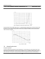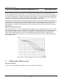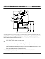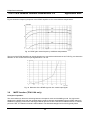
1
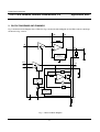
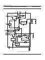
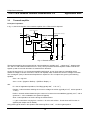
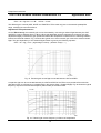
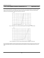
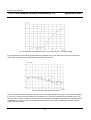
APPLICATION NOTE
Application of the TEA1118
and TEA1118A versatile
cordless transmission circuits
AN96071
Philips
Semiconductors
Philips Semiconductors
TEA1118/A versatile cordless transmission ICs
Application Note
Abstract
The TEA1118 and TEA1118A are bipolar transmission circuits for use in cordless telephone sets or answering
machines. They are part of TEA111x family.
A detailed description of the circuit blocks of the TEA1118 and TEA1118A and advices on adjustments are
contained in this report.
2
Philips Semiconductors
TEA1118/A versatile cordless transmission ICs
Application Note
APPLICATION NOTE
Application of the TEA1118
and TEA1118A versatile
cordless transmission circuits
AN96071
Author:
JM Malaurie
Technical Marketing, Telecom Products
Caen, France
Keywords
Telecom
Demonstration Board
TEA1118
TEA1118A
Transmit
DTMF
Receive
Date: July 31st, 1996
3
Philips Semiconductors
TEA1118/A versatile cordless transmission ICs
Application Note
Summary
A detailed description of the blocks of both ICs TEA1118 and TEA1118A is given. The possible settings to
adjust the DC and transmission characteristics are explained.
The TEA1118 and the TEA1118A incorporate a transmit amplifier and a receive amplifier, the TEA1118A
incorporates also a DTMF amplifier.
An evaluation board for the TEA1118A, which can be used for the TEA1118, is available.
The general notation in this report for both ICs is TEA1118/A.
Note:
The information presented in this document does not form part of any quotation or contract, is believed to be
accurate and reliable and may be changed without notice. No liability will be accepted by the publisher for any
consequence of its use. Publication thereof does not convey nor imply any licence under patent or other
industrial property rights.
4
Philips Semiconductors
TEA1118/A versatile cordless transmission ICs
Application Note
CONTENTS
1. INTRODUCTION ...........................................................................................................................................7
2. BLOCK DIAGRAMS AND PINNINGS ...........................................................................................................8
3. DESCRIPTION OF THE TEA1118/A...........................................................................................................12
3.1 DC characteristics and supply block ......................................................................................................13
3.1.1 DC characteristics .......................................................................................................................13
3.1.2 Supply for peripherals .................................................................................................................16
3.2 Set impedance......................................................................................................................................17
3.3 Transmit amplifier .................................................................................................................................18
3.4 TMUTE function (TEA1118A only) ........................................................................................................22
3.5 Receive amplifier ..................................................................................................................................23
3.6 Automatic gain control...........................................................................................................................26
3.7 DTMF amplifier (TEA1118A only)..........................................................................................................27
3.8 MUTE function (TEA1118A only) ..........................................................................................................29
3.9 Anti-sidetone network............................................................................................................................31
3.9.1 TEA106x or TEA111x family bridge.............................................................................................31
3.9.2 Wheatstone bridge ......................................................................................................................32
4. APPLICATION COOKBOOK ......................................................................................................................33
5. EXAMPLE OF APPLICATION ....................................................................................................................35
6. ELECTROMAGNETIC COMPATIBILITY ....................................................................................................37
7. REFERENCES ............................................................................................................................................38
5
Philips Semiconductors
TEA1118/A versatile cordless transmission ICs
Application Note
LIST OF FIGURES
FIG. 1 TEA1118 BLOCK DIAGRAM .................................................................................................................................... 8
FIG. 2 TEA1118A BLOCK DIAGRAM ................................................................................................................................. 9
FIG. 3 TEA1118 PINNINGS..............................................................................................................................................10
FIG. 4 TEA1118A PINNINGS............................................................................................................................................11
FIG. 5 BASIC APPLICATION FOR MEASUREMENTS ...............................................................................................................12
FIG. 6 DC CHARACTERISTICS CONFIGURATION ..................................................................................................................13
FIG. 7 ICC VERSUS VCC.................................................................................................................................................14
FIG. 8 MAIN VOLTAGES VERSUS LINE CURRENT ................................................................................................................14
FIG. 9 LOW VOLTAGE BEHAVIOR IN LINE POWERED CONDITIONS ........................................................................................15
FIG. 10 LOW VOLTAGE BEHAVIOR WITH EXTERNAL POWER SUPPLY....................................................................................15
FIG. 11 INFLUENCE OF AN RVA RESISTOR BETWEEN REG AND SLPE ON VLN AT 15MA .....................................................16
FIG. 12 INFLUENCE OF RSLPE ON THE DC CHARACTERISTICS ............................................................................................16
FIG. 13 EQUIVALENT SET IMPEDANCE ...............................................................................................................................17
FIG. 14 TRANSMIT CHANNEL ............................................................................................................................................18
FIG. 15 TRANSMIT GAIN VERSUS RGAT CONNECTED BETWEEN GAT AND REG ..................................................................19
FIG. 16 TRANSMIT GAIN VERSUS FREQUENCY: INFLUENCE OF TEMPERATURE......................................................................19
FIG. 17 DISTORTION ON LINE VERSUS TRANSMIT SIGNAL AT NOMINAL GAIN ON TEA1118/A ..............................................20
FIG. 18 DISTORTION ON THE LINE VERSUS TRANSMIT SIGNAL AT 5 DB GAIN ON TEA1118..................................................20
FIG. 19 DISTORTION OF LINE SIGNAL AT ILINE = 4 MA WITH EXTERNAL 3.3 V POWER SUPPLY .............................................21
FIG. 20 TRANSMIT NOISE VERSUS LINE CURRENT ...............................................................................................................21
FIG. 21 COMMUN MODE REJECTION RATIO ON TRANSMIT ..................................................................................................22
FIG. 22 TRANSMIT GAIN AND TMUTE INPUT CURRENT VERSUS TMUTE INPUT VOLTAGE ..................................................22
FIG. 23 TRANSMIT GAIN REDUCTION IN TMUTE CONDITION ............................................................................................23
FIG. 24 RECEIVE CHANNEL...............................................................................................................................................23
FIG. 25 RECEIVE GAIN VERSUS RGAR CONNECTED BETWEEN GAR AND QR .......................................................................24
FIG. 26 RECEIVE GAIN VERSUS FREQUENCY AND TEMPERATURE ........................................................................................25
FIG. 27 DISTORTION ON QR VERSUS INPUT SIGNAL ON IR .................................................................................................25
FIG. 28 DISTORTION ON QR VERSUS LEVEL WITH 450 Ω LOAD..........................................................................................26
FIG. 29 NOISE ON QR .....................................................................................................................................................26
FIG. 30 AGC ON THE TRANSMIT GAIN VERSUS LINE CURRENT AND RAGC............................................................................27
FIG. 31 DTMF CHANNEL OF THE TEA1118A ..................................................................................................................28
FIG. 32 DTMF GAIN VERSUS FREQUENCY AT DIFFERENT TEMPERATURES ..........................................................................29
FIG. 33 DISTORTION OF THE DTMF SIGNAL ON LINE VERSUS INPUT SIGNAL .......................................................................29
FIG. 34 TRANSMIT GAIN AND MUTE INPUT CURRENT VERSUS MUTE INPUT VOLTAGE.......................................................30
FIG. 35 TRANSMIT AND RECEIVE GAIN REDUCTION IN MUTE CONDITION ON THE TEA1118A............................................30
FIG. 36 TEA106X ORTEA111X FAMILY ANTI-SIDETONE BRIDGE (LEFT) AND WHEATSTONE BRIDGE (RIGHT) ......................31
FIG. 37 EQUIVALENT AVERAGE LINE IMPEDANCE ..............................................................................................................32
FIG. 38 BASIC APPLICATION OF THE TEA1118A ...............................................................................................................36
6
Philips Semiconductors
TEA1118/A versatile cordless transmission ICs
Application Note
1. INTRODUCTION
The TEA1118/A offer all the transmit, receive and line interface functions required in cordless telephone sets or
in answering machines. They perform the interface between the line and the RF interface of a cordless
telephone set or between the line and the codecs of a digital answering machine.
Furthermore, the TEA1118A includes a DTMF amplifier for dialling. The selection between the transmit
amplifier and the DTMF amplifier is made with a MUTE or a TMUTE function. The MUTE function switches-off
both the transmit and the receive amplifiers while the TMUTE switches-off only the transmit amplifier, both
switch-on the DTMF amplifier.
The TEA1118 is mainly dedicated to applications where DTMF is not necessary (eg: answering machine
application) or where DTMF is provided by some other part (eg: DECT application). The TEA1118A is mainly
dedicated to CTO base stations.
The report is divided into two parts: the first part, up to chapter 3, gives a detailed description of the different
circuit blocks of the TEA1118/A including operating principles, settings of DC and transmission characteristics
and performances of the different functions; the second part describes the consecutive steps to design and
adjust applications using the TEA1118/A and introduces the demoboard.
Note: the values of parameters given in this application note are as accurate as possible, but please, refer to
the last product specification for final ones.
7
Philips Semiconductors
TEA1118/A versatile cordless transmission ICs
Application Note
2. BLOCK DIAGRAMS AND PINNINGS
Fig. 1 shows the block diagram of the TEA1118, fig. 2 shows the block diagram of the TEA1118A, the pinnings
are shown in fig. 3 and 4.
QR
GAR
IR
V
-
I
VCC
+
+
current
management
LN
TX+
TX-
V
GAT
I
REG
+
+
AGC
circuit
+
low voltage
circuit
VEE
SLPE
AGC
Fig. 1 TEA1118 block diagram
8
Philips Semiconductors
TEA1118/A versatile cordless transmission ICs
MUTE
IR
V
Application Note
QR
GAR
I
VCC
+
V
DTMF
+
I
current
management
LN
Att.
V
I
TMUTE Transmit mute
TX+
TX-
REG
V
I
+
+
AGC
circuit
+
low voltage
circuit
VEE
SLPE
AGC
Fig. 2 TEA1118A block diagram
9
Philips Semiconductors
TEA1118/A versatile cordless transmission ICs
LN
SLPE
REG
GAT
nc
nc
nc
nc
16
1
15
2
14
3
4 TEA1118M 13
12
5
11
6
10
7
9
8
VCC
GAR
QR
VEE
TX+
TXAGC
IR
LN
SLPE
REG
GAT
nc
nc
IR
Application Note
14
1
13
2
12
3
4 TEA1118T 11
10
5
6
9
7
8
Fig. 3 TEA1118 pinnings
TEA1118M PIN
TEA1118T PIN
NAME
DESCRIPTION
1
1
LN
Positive line terminal
2
2
SLPE
Slope adjustment
3
3
REG
Line voltage regulator decoupling
4
4
GAT
Transmit gain reduction adjustment
5
5
nc
Not connected
6
6
nc
Not connected
7
nc
Not connected
8
nc
Not connected
9
7
IR
Receive amplifier input
10
8
AGC
Automatic gain control
11
9
TX-
Inverting transmit input
12
10
TX+
Non inverting transmit input
13
11
VEE
Negative line terminal
14
12
QR
Receive amplifier output
15
13
GAR
Receive gain reduction adjustment
16
14
VCC
Supply voltage for speech and peripherals
10
VCC
GAR
QR
VEE
TX+
TXAGC
Philips Semiconductors
TEA1118/A versatile cordless transmission ICs
LN
SLPE
REG
nc
TMUTE
DTMF
nc
MUTE
VCC
GAR
QR
VEE
TX+
TXAGC
IR
1
16
2
15
3
14
4 TEA1118AM13
5
12
6
11
7
10
8
9
LN
SLPE
REG
TMUTE
DTMF
MUTE
IR
Application Note
1
14
2
13
3
12
4 TEA1118AT 11
5
10
6
9
7
8
Fig. 4 TEA1118A pinnings
TEA1118AM PIN
TEA1118AT PIN
NAME
DESCRIPTION
1
1
LN
Positive line terminal
2
2
SLPE
Slope adjustment
3
3
REG
Line voltage regulator decoupling
nc
Not connected
4
5
4
TMUTE
Transmit mute input
6
5
DTMF
Dual-tone multifrequency input
nc
Not connected
7
8
6
MUTE
Mute input
9
7
IR
Receive amplifier input
10
8
AGC
Automatic gain control
11
9
TX-
Inverting transmit input
12
10
TX+
Non inverting transmit input
13
11
VEE
Negative line terminal
14
12
QR
Receive amplifier output
15
13
GAR
Receive gain reduction adjustment
16
14
VCC
Supply voltage for speech and peripherals
11
VCC
GAR
QR
VEE
TX+
TXAGC
Philips Semiconductors
TEA1118/A versatile cordless transmission ICs
Application Note
3. DESCRIPTION OF THE TEA1118/A
All the curves shown in this section result from measurement of typical samples. All the component names refer
to the basic application of the ICs shown in fig. 5.
+Vcc
Cz
Peripheral
supply
Rcc
Rz
620 Ω
GND
+
0Ω
Cvcc
100 µF
VCC
1 LN
TX+
Rprot
10 Ω
Rast1
D2
A
D3
TX-
Dz
1N4004
Ctx1
TXA
Rtx3
Ctx2
TXB
Rtx1
130 kΩ
D1
Rtx2
10 V
D4
TEA1118/A
B
Cgar
Cgars
Cir
IR
1 nF
100 nF
GAR
100 pF
Rgar
Cear
∝
Ragc
AGC
REC
QR
0Ω
MUTE
MUTE
TMUTE
GAT/TMUTE 4
Rast2
3.92 kΩ
Cmf
DTMF
SLPE
Rast3
Rbal1
VEE
3
100 nF
Cgat
Rgat
∝
392 Ω
Rslpe
20 Ω
Cbal
REG
2
+ Creg
4.7 µF
Rbal2
Fig. 5 Basic application for measurements
12
DTMF
Philips Semiconductors
TEA1118/A versatile cordless transmission ICs
3.1
Application Note
DC characteristics and supply block
Without influence on the DC characteristics (except a slight difference at very low line current), the TEA1118/A
can be used in two different supply configurations: they can provide supply to peripheral circuits like any IC from
the TEA111x family of line interfaces or they can be externally supplied if an external power supply is available.
3.1.1
DC characteristics
Principle of operation
The ICs generate a stabilized voltage (called Vref) between pins LN and SLPE. This reference voltage, typically
3.35 V, is temperature compensated. The voltage at pin REG is used by the internal regulator to generate the
stabilized Vref voltage and is decoupled by a capacitor Creg connected to VEE.
For effective operation of the apparatus, the TEA1118/A must have a low resistance to the DC current and a
high impedance to speech signals. The Creg capacitor, converted into an equivalent inductance (see “set
impedance” section), realizes this impedance conversion from its DC value (Rslpe) to its AC value (Rcc
+Rz//Cz in the audio frequency range). The DC voltage at pin SLPE is proportional to the line current.
This general configuration is shown in fig. 6.
Rline
Rcc
VCC
LN
Rp
from preamp
Ip
Iline
Icc
Rexch
Rgasint
Iln
+
Vexch
Vd
+
Rd
+
Cvcc
VEE
REG
SLPE
+ Creg
Islpe
Rslpe
Fig. 6 DC characteristics configuration
The ICs regulate the line voltage between pins LN and SLPE. the voltage on pin LN can be calculated as:
Vln = Vref + Rslpe × Islpe
Islpe = Iline - Icc - Ip - Iln
Iline = line current
Icc = current consumption of the IC
Ip = supply current for peripherals
Iln = Current consumption between LN and VEE
13
Philips Semiconductors
TEA1118/A versatile cordless transmission ICs
Application Note
The DC line current Iline flowing into the apparatus is determined by the exchange supply voltage Vexch, the
feeding bridge resistance Rexch, the DC resistance of the telephone line Rline and the voltage across the
apparatus including diode bridge.
Below a threshold line current Ith (typically equal to 7.5 mA) the internal reference voltage (generating Vref) is
automatically adjusted to a lower value (down to an absolute minimum voltage of 1.6 V). In this range, the
shape of the curve giving Vref versus line current is slightly different if VCC is used to supply peripheral circuits
or if the TEA1118/A are supplied from external supply. This means that more sets can operate in parallel or that
for very low voltage feeding bridge the line current has a higher value. For line currents below this threshold
current, the TEA1118/A has reduced sending and receiving performances. This is called the low voltage area.
The internal circuitry of the TEA1118/A is supplied from pin VCC. In line powered application, this voltage is
derived from the line voltage by means of a resistor (Rcc) and must be decoupled by a capacitor (Cvcc). Fig. 7
shows the IC current consumption (Icc) as a function of the VCC supply voltage.
Fig. 7 Icc versus VCC
Fig. 8 shows the main voltages as a function of the line current.
Fig. 8 Main voltages versus line current
14
Philips Semiconductors
TEA1118/A versatile cordless transmission ICs
Application Note
Fig. 9 shows the behavior in the low voltage area in line powered condition while fig. 10 shows this behavior
when the ICs are externally powered.
Fig. 9 Low voltage behavior in line powered conditions
Fig. 10 Low voltage behavior with external 3.3 V power supply
Adjustments and performances
The reference voltage, Vref, can be adjusted by means of an external resistor Rva. It can be increased by
connecting the Rva resistor between pins REG and SLPE (see fig; 11), or decreased by connecting the Rva
resistor between pins REG and LN. In case of line powered application, it is not recommended to use the
voltage reduction because it reduces the peripheral supply capability. To ensure correct operation, it is not
advised to adjust Vref at a value lower than 3 V or higher than 7 V (the maximum operating voltage of 12 V
must be guaranteed by the application). These adjustments will slightly affect a few parameters: there will be a
small change in the temperature coefficient of Vref and a slight increase in the spread of this voltage reference
due to matching between internal and external resistors. Furthermore, the Rva resistor connected between
REG and LN will slightly affect the apparatus impedance(see section “set impedance”).
15
Philips Semiconductors
TEA1118/A versatile cordless transmission ICs
Application Note
Fig. 11 Influence of an Rva resistor between REG and SLPE on Vln at 15mA
The DC slope of the voltage on pin LN is influenced by the Rslpe resistor as shown in fig. 12. The preferred
value for Rslpe is 20 Ω, changing this value will affect more than the DC characteristics, it also influences the
gains, the AGC characteristics, the maximum output swing on the line and the low voltage threshold Ith.
Fig. 12 Influence of Rslpe on the DC characteristics
3.1.2
Supply for peripherals
This sub-chapter concerns line powered applications which may not be usual for these ICs.
Principle of operation
The supply voltage at pin VCC is normally used to supply the internal circuitry of the TEA1118/A. However, a
small current can be drawn to supply peripheral circuits having VEE as ground reference. The VCC supply
voltage depends on the current consumed by the IC and the peripheral circuits as shown by the following
formula:
VCC = VCC0 - Rccint × (Iqr + Ip)
VCC0 = VLN - Rcc × Icc
Iqr = internal current necessary to supply the receive output amplifier when there is AC signal
Rccint = Rcc // internal equivalent impedance between VCC and VEE
16
Philips Semiconductors
TEA1118/A versatile cordless transmission ICs
Application Note
Rccint is the output impedance of the voltage supply point. As can be seen from fig. 7, the internal supply
current Icc depends on the voltage on the pin VCC, it means that the impedance of the internal circuitry
connected between VCC and VEE is not infinite. While supplying a peripheral circuit on VCC, the Ip supply
current flowing through the Rcc resistor decreases the value of the voltage on the pin VCC and then reduces
the Icc consumption. So, the impedance to use in combination with Ip and Iqr is not Rcc but Rccint which
include in parallel the impedance of the internal circuitry connected between VCC and VEE. For a line current
equal to 15 mA and Rcc equal to 620 Ω, this Rccint impedance is 550 Ω.
As VCC is limited to a minimum value to ensure correct operation, Ip will be limited to a maximum value.
Adjustments and performances
As the impedance connected between LN and VCC also determines the set impedance, the easiest way to
increase the current capability of the supply point VCC is to increase the reference voltage Vref by connecting a
resistor Rva between pins REG and SLPE (see 3.1.1).
3.2
Set impedance
Principle of operation
The ICs behave like an equivalent inductance that presents a low impedance to DC (Rslpe) and a high
impedance (Rp) to speech signals. Rp is an integrated resistance in the order of 15.5 kΩ +/-15%. It is in parallel
with the external RC realized by Rcc and Cvcc. Thus, in the audio frequency range, the apparatus impedance
(called set impedance) is mainly determined by the Rcc resistor. Fig. 13 shows an equivalent schematic for the
set impedance.
LN
Leq
Vref
Rp
Rcc
REG
VCC
Leq = Creg x Rslpe x Rp
Rp = internal resistor
SLPE
+
Rslpe
20 Ω
Creg
4.7 µF
+
Cvcc
100 µF
VEE
Fig. 13 Equivalent set impedance
Adjustments and performances
When decreasing the reference voltage Vref, a resistor is connected between LN and REG in parallel of Rp
(see fig. 13) so, slightly modifying the impedance.
If complex set impedance is required, the Rcc resistor resistor is replaced by a complex network (see fig. 5 :Rcc
+ Rz // Cz). The DC resistance which influences the value of VCC becomes Rcc + Rz.
17
Philips Semiconductors
TEA1118/A versatile cordless transmission ICs
3.3
Application Note
Transmit amplifier
Principle of operation
In fig. 14, the block diagram of the transmit amplifier of the TEA1118/A is depicted.
from DTMF
(TEA1118A only)
GAT (TEA1118 only)
TX+
TX-
V
I
LN
Rp
AGC
circuit
+
Rgasint
-
Rcc
Rexch
+
Rd
SLPE
REG
+ Creg
Rslpe
+ Cvcc
+ Cexch
Fig. 14 Transmit channel
The transmit amplifier has symmetrical high input impedances (typically 64 kΩ -2 times 32 kΩ- between pins
TX+ and TX- with maximum tolerances of +/- 15%). The input of this transmit amplifier is able to handle AC
signals up 900 mVrms with less than 2% total harmonic distortion.
As can be seen from fig. 14, the transmit amplifier itself is built up out of two parts: a preamplifier which
realizes a voltage to current conversion, and an end-amplifier which realizes the current to voltage conversion.
The overall gain (Gvtx) of the transmit amplifier from inputs TX+/TX- to output LN is given by the following
equation:
Gvtx = 20 × log Avtx
Avtx = 0.016 × (Rgasint / Rrefint) × (Ri//Zline / Rslpe) × α
with:
Ri = the AC apparatus impedance, Rcc//Rp (typically 620 Ω // 15.5 kΩ)
Rgasint = internal resistor realizing the current to voltage conversion (typically 27.6 kΩ with a spread of
+/-15%)
Rrefint = internal resistor determining the current of an internal current stabilizer (typically 3.4 kΩ with a
spread of +/- 15% correlated to the spread of Rgasint)
Zline = load impedance of the line during the measurement
α = gain control factor varying from 1 at Iline = 15 mA to 0.5 at Iline = 75 mA when AGC function is
applied (see chapter 3.6 for details)
Using these typical values in the equation and assuming Zline = 600 Ω, we find a gain equal to:
18
Philips Semiconductors
TEA1118/A versatile cordless transmission ICs
Gvtx = 20 × log Avtx = 11 dB
Application Note
at Iline = 15 mA
The different gain controls (AGC; MUTE and TMUTE for TEA1118A only) act on the transmit preamplifier
stage, modifying its transconductance.
Adjustments and performances
On the TEA1118 only, the transmit gain can be decreased by connecting a resistor Rgat between pins GAT
and REG. It can be adjusted from 11 dB to 5 dB to suit application specific requirements, however, this gain
adjustment slightly increases the gain spread and affects the temperature coefficient due to matching between
internal and external resistors. Fig. 15 shows the typicall curve of the transmit gain versus the external resistor
Rgat. The gain dependancy to this external Rgat resistor is given by the following equation:
Gvtx = 20 × log [ 0.016 × (Rgasint//Rgat / Rrefint) × (Ri//Zline / Rslpe) × α ]
Fig. 15 Transmit gain versus Rgat connected between GAT and REG
A capacitor Cgat can be connected between pins GAT and REG of the TEA1118 to provide a first order lowpass filter which cut-off frequency is determined by the product Cgat × (Rgasint//Rgat). Fig 16 shows the typical
frequency response of the transmit amplifier (without filter) of the TEA1118/A.
Fig. 16 Transmit gain versus frequency: influence of temperature
19
Philips Semiconductors
TEA1118/A versatile cordless transmission ICs
Application Note
Fig 17 shows the distortion of the signal on the line as a function of the transmit signal at nominal DC settings
and for a line current of 15 mA for TEA1118/A, while fig. 18 shows this distortion versus the input transmit
signal when the transmit gain is reduced to 5 dB on the TEA1118.
Fig. 17 Distortion on line versus transmit signal at nominal gain on TEA1118/A
Fig. 18 Distortion on the line versus transmit signal at 5 dB gain on TEA1118
Fig. 19 shows the distortion of the line signal versus the input transmit signal on the line at line current of 4 mA
and nominal gain when the TEA1118/A are powered from an external 3.3 V power supply between VCC and
VEE.
20
Philips Semiconductors
TEA1118/A versatile cordless transmission ICs
Application Note
Fig. 19 Distortion of line signal at Iline = 4 mA with external 3.3 V power supply
Fig. 20 shows the transmit noise (psophometrically weighted: P53 curve) versus line current at nominal gain
when a 200 Ω resistor is connected between the inputs TX+ and TX-.
Fig. 20 Transmit noise versus line current
Fig. 21 shows the common mode rejection ratio at 15 mA and at nominal transmit gain. Two curves are present
in this fig. 21, the first one is the spectrum of the signal on pin LN when a transmit signal is applied on pin TXwhile pin TX+ is shorted to VEE, the second one is the spectrum of the signal on pin LN when a transmit signal
is applied on pins TX- and TX+ shorted together. Both signals are at 1 kHz, the difference between the two
curves gives the CMRR.
21
Philips Semiconductors
TEA1118/A versatile cordless transmission ICs
Application Note
Fig. 21 Common mode rejection ratio on transmit
3.4
TMUTE function (TEA1118A only)
Principle of operation
The transmit mute function realizes an electronic switching between the transmit amplifier and the sending
DTMF amplifier. This function disables the transmit channel to provide a kind of privacy function and at the
same time enables the DTMF channel if needed for some specific applications; this function has no effect on
the receive channel. If a high level is applied to the TMUTE input, the transmit channel is disabled while the
DTMF channel is enabled, by applying a low level or leaving pin TMUTE open (if MUTE pin level is low) the
transmit channel is enabled. The threshold voltage level is 0.68 V typically with a temperature coefficient of -2
mV/°C. Fig. 22 shows the transmit gain reduction and TMUTE input current versus TMUTE input voltage.
Fig. 22 Transmit gain and TMUTE input current versus TMUTE input voltage
Adjustment and performances
Fig. 23 shows the transmit amplifier gain reduction at Iline = 15 mA for an input signal of 1 kHz. Two curves are
present on this fig. 23, the first one shows the spectrum of the signal on the line when a signal is applied on the
transmit inputs and when TMUTE is at a low level, the second one shows the same signal when pin TMUTE is
at a high level. The difference between the two curves at this frequency gives the gain reduction.
22
Philips Semiconductors
TEA1118/A versatile cordless transmission ICs
Application Note
Fig. 23 Transmit gain reduction in TMUTE condition
The TMUTE function works down to a voltage on VCC equal to 1.6 V, below this threshold, the transmit
amplifier stays always enabled independently of the TMUTE input level. The maximum voltage allowed at pin
TMUTE is VCC +0.4 V.
3.5
Receive amplifier
Principle of operation
In fig. 24, the block diagram of the receive amplifier is depicted.
MUTE
(TEA1118A only)
GAR
Rgarint
IR
V
I
+
AGC
V
DTMF
(TEA1118A only)
Vcc/2
I
Att.
Fig. 24 Receive channel
23
QR
Philips Semiconductors
TEA1118/A versatile cordless transmission ICs
Application Note
The receive amplifier has an a-symmetrical high input impedance between pins IR and VEE. It is equal to 20 kΩ
with a maximum tolerance of +/-15%. The ICs are able to drive loads down to an impedance of 150 Ω. As can
be seen from fig. 24, the receive amplifier itself is built up out of two parts: a preamplifier which realizes a
voltage to current conversion and an end-amplifier which realizes the current to voltage conversion. The overall
gain Gvrx of the receive amplifier from input IR to output QR is given by the equation:
Gvrx = 20 × log Avrx
Avrx = α × 1.21 × Rgarint/Rrefint
with:
Rgarint = internal resistor realizing the current to voltage conversion (typically 100 kΩ with a spread of
+/-15%)
Rrefint = internal resistor determining the current of an internal current stabilizer (typically 3.4 kΩ with a
spread of +/- 15% correlated to the spread of Rgasint)
α = gain control factor varying from 1 at Iline = 15 mA to 0.5 at Iline = 75 mA when AGC function is
applied (see chapter 3.6 for details)
Using these typical values in the equation, we find a gain equal to:
Gvrx = 20 × log Avrx = 31 dB
at Iline = 15 mA
The different gain controls (AGC; MUTE for TEA1118A only) act on the receive preamplifier stage, modifying its
transconductance.
Adjustments and performances
The receive gain can be decreased on the TEA1118/A by connecting a resistor Rgar between pins GAR and
QR. It can be decreased from 31 dB down to 19 dB to suit application specific requirements, however, this gain
adjustment slightly increases the gain spread and affects the temperature coefficient due to matching between
internal and external resistors. 31 dB of receive gain compensate almost typically the attenuation provided by
the antisidetone network. Fig. 25 shows the typicall curve of the receive gain versus the external resistor Rgar.
The gain dependancy to this external Rgar resistor is given by the following equation:
Gvrx = 20 × log [ 1.21 × (Rgarint//Rgar / Rrefint) × α ]
Fig. 25 Receive gain versus Rgar connected between GAR and QR
24
Philips Semiconductors
TEA1118/A versatile cordless transmission ICs
Application Note
Two external capacitors Cgar (connected between GAR and QR) and Cgars (connected between GAR and
VEE) ensure stability when the relationship Cgars ≥ 10 × Cgar is fulfilled. The Cgar capacitor provides a first
order low pass filter, which cut-off frequency is determined with Rgarint//Rgar. Fig. 26 shows the frequency
response of the receive amplifier at different temperatures (Cgar = 100 pF, Cgars = 1 nF).
Fig. 26 Receive gain versus frequency and temperature
The maximum output swing on QR depends on the DC line voltage, the Rcc resistor, the Icc current
consumption of the circuit, the Ip current consumption of the peripheral circuits and the load impedance on QR.
The receiving input IR can handle signals up to 18 mVrms with less than 2% THD. Fig. 27 shows the distortion
on QR when the limitation is related to the input voltage for a line current equal to 75 mA. Fig. 28 shows the
distortion of the signal on QR as a function of the rms signal on QR with a load of 450 Ω and a line current of 15
mA.
Fig. 27 Distortion on QR versus input signal on IR
25
Philips Semiconductors
TEA1118/A versatile cordless transmission ICs
Application Note
Fig. 28 Distortion on QR versus level with 450 Ω load
Fig. 29 shows the noise on QR loaded with 150 Ω (psophometrically weighted: P53 curve) as a function of the
line current. This curve has been done with an open input IR. With the antisidetone network connected to the
input IR, part of the transmit noise generated on the line will be added but, thanks to the low transmit noise
value, the effect is negligible.
Fig. 29 Noise on QR
3.6
Automatic gain control
Principle of operation
The TEA1118/A perform automatic line loss compensation. The automatic gain control varies the gain of the
transmit and receive amplifiers in accordance with the DC line current. To enable this AGC function, the pin
AGC must be connected to the pin VEE. For line currents below a current threshold, Istart (typically 25 mA), the
gain control factor α is equal to 1, giving the maximum value to the gains Gvtx and Gvrx. If this threshold
26
Philips Semiconductors
TEA1118/A versatile cordless transmission ICs
Application Note
current is exceeded, the gain control factor α is reduced and then the gains of the controlled transmit and
receive amplifiers are also reduced. When the line current reaches an other threshold current, Istop (typically 63
mA), the gain control factor α is limited to its minimum value equal to 0.5, giving the lower value to the transmit
and receive controlled gains. The gain control range of both amplifiers is typically 5.8 dB, which corresponds to
a line length of 5 km (0.5 mm twisted pair copper) with an attenuation of 1.2 dB/km.
The attenuation is correlated to the current Iagc sunk at pin AGC: when this current is lower than typically 5 µA
the gains are maximum, when this current is higher than typically 13 µA the gains are minimum. This current is
proportional to the voltage between pins SLPE and VEE. There is an internal resistor which sets Istart and
Istop, adding one externally in series (between pins AGC and VEE) reduces Iagc and increases the values of
Istart and Istop.
Adjustments and performances
The ICs are optimized for use with an exchange supply voltage of 48 V, a feeding bridge of 2 × 300 Ω and the
line previously described. In order to fit with other configurations, a resistor Ragc, can be inserted between pins
AGC and VEE. This Ragc resistor increases the two threshold currents Istart and Istop. Fig. 30 shows the
control of the transmit gain versus the line current for different values of Ragc. When no AGC function is
required, the AGC pin must be left open, then the control factor α equals to 1 and both controlled gains are at
their maximum values.
Fig. 30 AGC on the transmit gain versus line current and Ragc
3.7
DTMF amplifier (TEA1118A only)
principle of operation
In fig. 31, the block diagram of the DTMF channel of the TEA1118A is depicted.
27
Philips Semiconductors
TEA1118/A versatile cordless transmission ICs
MUTE
GAR
from transmit
preamp
Application Note
QR
Rgarint
-
Att.
24 dB
V
I
+
VCC/2
DTMF
TMUTE
Att.
20 dB
V
I
from receive
preamp
LN
Transmit mute
Rp
Rgasint
+
Rcc
-
Rexch
+
Rd
REG
+
SLPE
Cvcc
Rslpe +
+ Cexch
Fig. 31 DTMF channel of the TEA1118A
The DTMF amplifier has an a-symmetrical high input impedance of 20 kΩ between pins DTMF and VEE with a
maximum spread of +/-15%. The DTMF amplifier is built up out of three parts: an attenuator by a factor of 10, a
preamplifier which realizes the voltage to current conversion and the same end-amplifier as the transmit
amplifier. No AGC is applied to the DTMF channel. The overall gain (Gvmf) of the DTMF amplifier from input
DTMF to output LN is given by the following equation:
Gvmf = 20 × log Avmf
Avmf = 0.032 × (Rgasint / Rrefint) × (Ri//Zline / Rslpe)
with:
Ri = the AC apparatus impedance, Rcc//Rp (typically 620 Ω // 15.5 kΩ)
Rgasint = internal resistor realizing the current to voltage conversion (typically 27.6 kΩ with a spread of
+/-15%)
Rrefint = internal resistor determining the current of an internal current stabilizer (typically 3.4 kΩ with a
spread of +/- 15% correlated to the spread of Rgasint)
Zline = load impedance of the line during the measurement
Using these typical values in the equation and assuming Zline = 600 Ω, we find a gain equal to:
Gvmf = 20 × log Avmf = 17.4 dB
28
Philips Semiconductors
TEA1118/A versatile cordless transmission ICs
Application Note
Fig. 32 shows the frequency response of the DTMF amplifier at 15 mA and different temperatures.
Fig. 32 DTMF gain versus frequency at different temperatures
The input of the DTMF amplifier can handle signals up to 180 mVrms with less than 2% THD. Fig. 33 shows the
distortion on line versus the rms input signal at Iline = 15 mA.
Fig. 33 Distortion of the DTMF signal on line versus input signal
3.8
MUTE function (TEA1118A only)
Principle of operation
The mute realizes an electronic switching between the speech mode and the dialling mode. If a high level is
applied to the MUTE input, both the transmit and the receive channels are disabled while the DTMF channel is
enabled. By applying a low level or leaving pin MUTE open the receive channel is enabled moreover, if TMUTE
pin level is low, the transmit channel is also enabled. The threshold voltage level is 0.68 V typically with a
29
Philips Semiconductors
TEA1118/A versatile cordless transmission ICs
Application Note
temperature coefficient of -2 mV/°C. Fig. 34 shows the transmit gain reduction and MUTE input current versus
MUTE input voltage.
Fig. 34 Transmit gain and MUTE input current versus MUTE input voltage
Adjustments and performances
Fig. 35 shows the transmit and receive amplifier gain reduction at Iline = 15 mA for an input signal of 1 kHz.
Two curves are present on these graphics, the first one shows the spectrum of the signal on the line ( or on
QR) when a signal is applied on the transmit inputs (or respectively on IR) and when MUTE is at a low level, the
second one shows the same signal when pin MUTE is at a high level. The difference between the two curves
at this frequency gives the gain reduction.
Fig. 35 Transmit and receive gain reduction in MUTE condition on the TEA1118A
The MUTE function works down to a voltage on VCC equal to 1.6 V, below this threshold, the transmit and
receive amplifiers stays always enabled independently of the MUTE input level. The maximum voltage allowed
at the MUTE input is VCC + 0.4 V.
30
Philips Semiconductors
TEA1118/A versatile cordless transmission ICs
3.9
Application Note
Anti-sidetone network
Principle of operation
To avoid the transmit signal to come back with a too high level in the receive channel, the anti-sidetone circuit
uses the transmit signal from pin SLPE (which is in opposite phase) to cancel the transmit signal at the IR input
of the receive amplifier. The anti-sidetone bridge already used for the TEA106x or the TEA111x families or a
conventional Wheatstone bridge as shown in fig. 36 may be used for the design of the anti-sidetone network.
LN
LN
Rcc
Zline
Zbal
VEE
VEE
IR
Itr
Zir
Rslpe
Rast1
Rast1
Rcc
Zline
Itr
IR
QR
Zir
QR
Rast2
Ra
Rslpe
Rast3
SLPE
SLPE
Zbal
Fig. 36 Wheatstone bridge (left) and TEA106x orTEA111x family anti-sidetone bridge (right)
The TEA106x or TEA111x family anti-sidetone bridge has the advantage of a relative flat transfer function in the
audio frequency range between the input IR and the output QR, both with real and complex set impedances.
Furthermore, the attenuation of the bridge for the receive signal (between pins LN and IR) is independent of the
value chosen for Zbal after the set impedance has been fixed and the condition shown in equation (6) is fulfilled.
Therefore, readjustment of the overall receive gain is not necessary in many cases.
Compare to the previous one the Wheatstone bridge has the advantages of needing one resistor less and a
smaller capacitor in Zbal. But the disadvantages include the dependence of the attenuation of the bridge on the
value chosen for Zbal and the frequency dependence of that attenuation. This requires some readjustment of
the overall receive gain.
3.9.1
TEA106x or TEA111x family bridge
The anti-sidetone circuit is composed of: Rcc//Zline, Rast1, Rast2, Rast3, Rslpe and Zbal. Maximum
compensation is obtained when the following conditions are fulfilled:
Rslpe × Rast1 = Rcc × ( Rast2 + Rast3 )
(6)
k = [Rast2 × ( Rast3 + Rslpe )] / ( Rast1 × Rslpe )
Zbal = k × Zline
The scale factor k is chosen to meet the compatibility with a standard value of capacitor for Zbal.
In practice, Zline varies strongly with line lenght and line type. Consequently, the value for Zbal has to be
chosen to fit with an average line length giving acceptable sidetone suppression with short and long lines. The
suppression further depends on the accuracy with which Zbal equals this average line impedance.
Example
Let’s optimize for a theorical equivalent average line impedance shown in Fig. 37.
31
Philips Semiconductors
TEA1118/A versatile cordless transmission ICs
Application Note
1265 Ω
210 Ω
140 nF
Fig. 37 Equivalent average line impedance
For compatibility of the capacitor value in Zbal with a standard capacitor value from the E6 series (220 nF):
k = 140 / 220 = 0.636
For Rast2, a value of 3.92 kΩ has been chosen. So, using the previous equations, we can calculate Zbal,
Rast1, Rast3. We find Rast1 = 130 kΩ, Rast3 = 390 Ω, and for Zbal 130 Ω in series with 220 nF // 820 Ω.
The attenuation of the receive line signal between LN and IR can be derivated from the following equation:
Vir / Vln = ( Zir // Rast2 ) / [ Rast1 + ( Zir // Rast2 )]
If Rast2 >> ( Rast3 // Zbal ).
With the values used in this example, it gives 32 dB at 1 kHz.
Zir is the receive amplifier input impedance, typically 20 kΩ.
3.9.2
Wheatstone bridge
The conditions for optimum suppression are given by:
Zbal = ( Rast1 / Rslpe ) × ( Rcc // Zline)
Also, for this bridge type, a value for Zbal has to be chosen that corresponds with an average line length.
The attenuation of the received line signal between LN and IR is given by:
Vir / Vln = ( Zir // Rast1 // Ra ) / [ Zbal + ( Zir // Rast1 // Ra )]
Ra is used to adjust the bridge attenuation; its value has no influence on the balance of the bridge.
32
Philips Semiconductors
TEA1118/A versatile cordless transmission ICs
Application Note
4. APPLICATION COOKBOOK
In this chapter, the procedure for making a basic application is given. Reffering to fig. 38, the design flow is
given as a number of steps which should be made. As far as possible for every step, the components involved
and their influence on every step are given.
Step
Adjustment
DC setting :
Adjust the DC setting of the TEA1118/A to the local PTT requirements.
Voltage LN-VEE
This voltage can be adjusted by changing Vref: increased up to 7 V with a
resistor between pins REG and SLPE or decreased down to 3 V with a
resistor between REG and LN.
DC slope
The DC slope might be modified by changing the value of Rslpe (this is not
advised: all gains are modified, AGC characteristic is modified).
Supply point VCC
In line powered applications, depends on the values of Vref and the resistive
part of the impedance network (Rcc + Rz).
External power supply can be applied.
Artificial inductor
Its value can be adjusted by changing the value of Creg: a smaller value
speeds-up the DC current shape during transients but decreases the value of
the inductance and then affects the BRL.
Impedance and sidetone :
After setting the required set impedance, the sidetone has to be optimized using the sidetone network in
order to minimize the loop gain in all line conditions. AGC can be adjusted at that step.
Application impedance
The BRL is adjusted with the impedance network connected between LN and
VCC (Rcc + Rz//Cz).
Sidetone
Adjust Zbal (Rbal1, Rbal2, Cbal) according to the line characteristics.
AGC
Internally defined, the characteristics (Istart and Istop) can be shiftted to
higher line currents with an external Ragc resistor connected between AGC
and VEE.
33
Philips Semiconductors
TEA1118/A versatile cordless transmission ICs
Step
Application Note
Adjustment
TEA1118/A transmit and receive gains
Transmit gain
The transmit gain of the application has to be adjusted preferably before
entering pins TX+/TX- for the TEA1118/A.
For the TEA1118 only, it is also possible to reduce the transmit gain with the
resistor Rgat.
Ctx1, Ctx2 and TX+/TX- input impedance form a high-pass filter.
A capacitor Cgat in parallel with the transmit gain resistor (between TEA1118
pins REG and GAT) form a low-pass filter.
Receive gain
The receive gain of the application has to be adjusted preferably after the
output QR, nevertheless, it is possible to reduce the receive gain with the
resistor Rgar.
A capacitor in parallel with the receive gain resistor (between TEA1118/A
pins QR and GAR) form a low-pass filter, stability is ensured with capacitor
Cgars (>10 × Cgar) between pins GAR and VEE.
TEA1118A only DTMF gain
DTMF
The DTMF level on line must be adjusted before entering pin DTMF. It is
selected with a high level either on pin TMUTE or on pin MUTE.
34
Philips Semiconductors
TEA1118/A versatile cordless transmission ICs
Application Note
5. EXAMPLE OF APPLICATION
A demo board (OM4789) is available, as the TEA1118/A may be used in various applications, this demo board
includes only the TEA1118A with its basic environment. Replacing the TEA1118A by a TEA1118 may make it
usable also for the evaluation of the TEA1118 which offers the possibility to reduce the transmit gain.
Fig. 38 gives the basic application of the TEA1118/A. On this schematic, the capacitors connected with doted
lines and the resistors drawn with dotted lines are indicated for RFI immunity purpose.
35
Philips Semiconductors
TEA1118/A versatile cordless transmission ICs
Application Note
Cz
+VCC
Rcc
Cvcc
+
Rz
0Ω
619 Ω
100 µF
C13
14
VCC
1 LN
2.2 nF
C1
Rprot
LNP
10 Ω
Rast1
C12
Dz
TX+
10
1 nF
10 V
D1
D3
A
D2
Ctx2
1 kΩ
100 nF
Rtx1
Ctx1
1 kΩ
100 nF
1 nF
TXP
Rtx3
∝
130 kΩ
C11
TX-
4.7 nF
1N4004
Rtx2
9
U1
D4
B
C10
7
(TEA1118T)
Cgar
Cgars
IR
100 pF
1 nF
Rgar
GAR 13
100 nF
Ragc
C2
1 nF
TEA1118AT
1 nF
Cir
TXM
8 AGC
+
∝
QR 12
Cear
10 µF
0Ω
RX
C6
1 nF
LNM
MUTE
TMUTE
Rast2
MUTE
6
3.92 kΩ
STR2
DTMF 5
SLPE
Rast3
Rbal1
330 Ω
VEE
2
REG
11
100 nF
3
Cmf
MF
100 nF
Cgat
Rgat
392 Ω
Rslpe
20 Ω
Cbal
TMUTE
STR1
4
(GAT)
Rbal2
+ Creg
C9
4.7 µF
1 nF
1.5 kΩ
GND
Fig. 38 Basic application of the TEA1118A
36
Philips Semiconductors
TEA1118/A versatile cordless transmission ICs
Application Note
6. ELECTROMAGNETIC COMPATIBILITY
As no common international specification exists for RFI immunity, and as different assembly methods may lead
to different solutions, only some advices can be provided.
It is advisable to take care of the impedance of the GND, the smallest is always the best. This means that the
GND (VEE) trace must always be as large as possible, the best is to have a second layer dedicated to this
purpose.
TX+/TX- inputs may also be sensitive (RF signals entering these pins would be amplified). Care has to be taken
with the lay-out of the transmit amplifier, which is also helpfull for the noise, providing a good decoupling to
GND. A low-pass RC filter may be added at the input of the amplifier.
Low impedance capacitors in parallel with the electrolythic one between VCC and GND as well as in parallel
with the Creg capacitor may help.
Usually a low impedance capacitor connected between LN and GND helps for the conducted interferences, but
this capacitor is in parallel with the impedance network of the apparatus, so, its value must be small enough.
In general when connections are coming from external environment (e.g. TXP, TXM, A, B on the demoboard), it
is better to filter the RFI signal before it influences the close environment of the TEA1118/A (e.g. action of
C1,C2,C11 on the demoboard).
37
Philips Semiconductors
TEA1118/A versatile cordless transmission ICs
7. REFERENCES
[1] TEA1118/A Versatile cordless transmission circuit
Device specification
[2] TEA1118/A Line Interface Demonstration Board
USER MANUAL of OM4789 (report n°: CTT96001)
[3] Philips Semiconductors
SEMICONDUCTORS FOR TELECOM SYSTEMS -IC03-
38
Application Note
Philips Semiconductors
TEA1118/A versatile cordless transmission ICs
Application Note
APPENDIX LIST OF ABBREVIATIONS AND DEFINITIONS
A-B
Line terminals of application example
AGC
Automatic Gain Control: line loss compensation
BRL
Balance Return Loss: matching between the apparatus impedance and a reference
DTMF
Dual Tone Multi Frequency
EMC
ElectroMagnetic Compatibility
GAR
Receive gain adjustment pin of the TEA1118/A
GAT
Transmit gain adjustment pin of the TEA1118
GND
Ground
Gvmf
DTMF amplifier gain
Gvrx
Receive gain
Gvtx
Transmit gain
IC
Integrated circuit
Icc
Current consumption of the TEA1118/A
Iline
Line current
Ip
Current consumption of the peripherals
Iqr
Internal current consumption (fromVCC) of the receive amplifier
IR
Receive amplifier input pin of the TEA1118/A
Islpe
Part of the line current flowing through SLPE pin
Istart
Start current of the AGC function
Istop
Stop current of the AGC function
Ith
Threshold current of the low voltage part
k
Scale factor of anti-sidetone network
Leq
Artificial inductor of the voltage stabilizer
MUTE
MUTE input of the TEA1118A
TMUTE
TMUTE input of the TEA1118A (transmit channel)
OM4789
Demoboard of the TEA1118A
QR
Receive amplifier output pin of the TEA1118/A
Ra
Resistor to adjust the sidetone bridge attenuation
Rast
Antisidetone resistor
REG
Filter capacitor of the equivalent inductor connection pin of the TEA1118/A
Rexch
Bridge resistance of exchange
RFI
Radio Frequency Interference
39
Philips Semiconductors
TEA1118/A versatile cordless transmission ICs
Rgar
External resistance to reduce receive gain of TEA1118/A
Rgarint
Internal resistance (100 kΩ) which sets the receive gain
Rgasint
Internal resistance (27 kΩ) which sets the transmit gain
Rgat
External resistance to reduce transmit gain of TEA1118
Rp
Internal resistance between LN and REG
SLPE
Slope input pin of the TEA1118/A
THD
Total Harmonic Distortion (%)
TX+/TX-
Transmit amplifier input pins of the TEA1118/A
VCC
Positive supply of the TEA1118/A
VEE
Ground reference of the TEA1118/A
Vln
DC voltage between LN and VEE
Vref
Stabilized reference voltage between LN and SLPE
Vslpe
DC voltage level between SLPE and VEE
Zir
Input impedance of the receive amplifier of the TEA1118/A
Zbal
Anti-sidetone network
α
Gain control factor of the AGC
40
Application Note