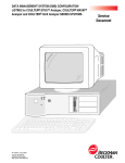
1
Intel® Xeon® Processor with 800
MHz System Bus, Intel® E7520
Chipset, and Intel® 6300ESB ICH
Development Kit
User’s Manual
March 2007
Order Number: 300281-006US
INFORMATION IN THIS DOCUMENT IS PROVIDED IN CONNECTION WITH INTEL® PRODUCTS. NO LICENSE, EXPRESS OR IMPLIED, BY ESTOPPEL OR
OTHERWISE, TO ANY INTELLECTUAL PROPERTY RIGHTS IS GRANTED BY THIS DOCUMENT. EXCEPT AS PROVIDED IN INTEL'S TERMS AND CONDITIONS
OF SALE FOR SUCH PRODUCTS, INTEL ASSUMES NO LIABILITY WHATSOEVER, AND INTEL DISCLAIMS ANY EXPRESS OR IMPLIED WARRANTY, RELATING
TO SALE AND/OR USE OF INTEL PRODUCTS INCLUDING LIABILITY OR WARRANTIES RELATING TO FITNESS FOR A PARTICULAR PURPOSE,
MERCHANTABILITY, OR INFRINGEMENT OF ANY PATENT, COPYRIGHT OR OTHER INTELLECTUAL PROPERTY RIGHT. Intel products are not intended for
use in medical, life saving, life sustaining, critical control or safety systems, or in nuclear facility applications.
Leg al Li nes and Dis clai mers
Intel may make changes to specifications and product descriptions at any time, without notice.
Intel Corporation may have patents or pending patent applications, trademarks, copyrights, or other intellectual property rights that relate to the
presented subject matter. The furnishing of documents and other materials and information does not provide any license, express or implied, by estoppel
or otherwise, to any such patents, trademarks, copyrights, or other intellectual property rights.
Designers must not rely on the absence or characteristics of any features or instructions marked “reserved” or “undefined.” Intel reserves these for
future definition and shall have no responsibility whatsoever for conflicts or incompatibilities arising from future changes to them.
Intel processor numbers are not a measure of performance. Processor numbers differentiate features within each processor family, not across different
processor families. See http://www.intel.com/products/processor_number for details.
The Intel® Xeon™ Processor, Intel® E7520 Chipset, Intel® 6300ESB ICH Development Kit may contain design defects or errors known as errata which
may cause the product to deviate from published specifications. Current characterized errata are available on request.
Hyper-Threading Technology requires a computer system with an Intel® Pentium® 4 processor supporting HT Technology and a HT Technology enabled
chipset, BIOS and operating system. Performance will vary depending on the specific hardware and software you use. See http://www.intel.com/
products/ht/Hyperthreading_more.htm for additional information.
Contact your local Intel sales office or your distributor to obtain the latest specifications and before placing your product order.
Copies of documents which have an order number and are referenced in this document, or other Intel literature may be obtained by calling
1-800-548-4725 or by visiting Intel's website at http://www.intel.com.
BunnyPeople, Celeron, Celeron Inside, Centrino, Centrino logo, Core Inside, Dialogic, FlashFile, i960, InstantIP, Intel, Intel logo, Intel386, Intel486,
Intel740, IntelDX2, IntelDX4, IntelSX2, Intel Core, Intel Inside, Intel Inside logo, Intel. Leap ahead., Intel. Leap ahead. logo, Intel NetBurst, Intel
NetMerge, Intel NetStructure, Intel SingleDriver, Intel SpeedStep, Intel StrataFlash, Intel Viiv, Intel vPro, Intel XScale, IPLink, Itanium, Itanium Inside,
MCS, MMX, Oplus, OverDrive, PDCharm, Pentium, Pentium Inside, skoool, Sound Mark, The Journey Inside, VTune, Xeon, and Xeon Inside are
trademarks or registered trademarks of Intel Corporation or its subsidiaries in the United States and other countries.
*Other names and brands may be claimed as the property of others.
Copyright © 2007, Intel Corporation. All Rights Reserved.
Intel® Xeon® Processor with 800 MHz System Bus, Intel® E7520 Chipset, and Intel® 6300ESB ICH Development Kit
UG
March 2007
2
Order Number: 300281-006US
Contents—Intel® Xeon™ Processor with 800 MHz System Bus, Intel® E7520 Chipset, and Intel ®
6300ESB ICH Development Kit
Contents
1.0
Product Overview ...................................................................................................... 6
1.1
Related Documents ............................................................................................. 6
1.2
Product Contents.................................................................................................6
1.3
Products Feature List ........................................................................................... 7
1.4
Block Diagram .................................................................................................... 8
1.4.1 Memory Subsystem ................................................................................ 10
1.4.2 DIMM Placement DDR2-400 ..................................................................... 10
1.5
Memory Population Rules and Configurations ........................................................ 11
2.0
Platform Management ............................................................................................. 12
2.1
Power Button.................................................................................................... 12
2.2
Soft Off............................................................................................................ 12
2.3
Sleep States Supported...................................................................................... 12
2.3.1 S0 State ............................................................................................... 12
2.3.2 S1 State ............................................................................................... 12
2.3.3 S2 State ............................................................................................... 13
2.3.4 S3 State ............................................................................................... 13
2.3.5 S4 State ............................................................................................... 13
2.3.6 S5 State ............................................................................................... 13
2.3.7 Wake-Up Events .................................................................................... 14
2.3.8 Wake-Up from S1 Sleep State .................................................................. 14
2.3.9 Wake-Up from S4 and S5 States .............................................................. 14
2.4
PCI PM Support................................................................................................. 14
2.5
Platform Management ........................................................................................ 14
2.5.1 Processor Thermal Management ............................................................... 14
2.6
System Fan Operation........................................................................................ 14
3.0
Equipment Required for CRB Usage ......................................................................... 16
3.1
Precautions ...................................................................................................... 16
3.2
Driver and OS Requirements............................................................................... 17
3.2.1 Drivers Included on CD ........................................................................... 17
4.0
Jumpers and Headers .............................................................................................. 21
4.1
Jumpers........................................................................................................... 21
5.0
System Overview..................................................................................................... 25
5.1
Power Diagrams ................................................................................................ 25
5.2
Platform Clocking .............................................................................................. 26
5.3
Platform Resets................................................................................................. 27
5.4
SMBus ............................................................................................................. 28
5.5
Platform IRQ Routing ......................................................................................... 29
5.6
VRD VID Headers .............................................................................................. 30
5.7
Miscellaneous Buttons ........................................................................................ 32
6.0
Debug Procedure ..................................................................................................... 33
6.1
Level 1 Debug (Port 80/BIOS)............................................................................. 33
6.2
Level 2 Debug (Power Sequence) ........................................................................ 34
6.3
Level 3 Debug (Voltage References)..................................................................... 34
7.0
Heatsink Assembly .................................................................................................. 35
7.1
Processor Heat Sink Installation Instructions ......................................................... 36
Intel® Xeon® Processor with 800 MHz System Bus, Intel® E7520 Chipset, and Intel ® 6300ESB ICH Development Kit
March 2007
UG
Order Number: 300281-006US
3
Intel ® Xeon™ Processor with 800 MHz System Bus, Intel® E7520 Chipset, and Intel® 6300ESB
ICH Development Kit—Contents
Figures
1
2
3
4
5
6
7
8
9
10
11
12
13
14
15
16
Customer Reference Board Block Diagram .................................................................... 8
Placement—Top View ................................................................................................. 9
DDR2-400 Memory - DIMM Ordering ...........................................................................11
Intel® Xeon® Processor with 800 MHz System Bus and Intel® E7520 and Intel®
6300ESB Customer Reference Board Jumper ................................................................21
Power Distribution Block Diagram ...............................................................................25
Clock Block Diagram .................................................................................................26
Platform Reset Diagram.............................................................................................27
SMBus Block Diagram ...............................................................................................28
IRQ Routing Diagram ................................................................................................29
Power Buttons..........................................................................................................32
Components Requiring Heat Sink Assembly..................................................................35
Inserting Processor in Socket .....................................................................................36
Cleaning the Processor Surface ..................................................................................37
Installing the Processor Backplate...............................................................................37
Removing the Protective Covers .................................................................................38
Installing the Heatsink ..............................................................................................38
Tables
1
2
3
4
5
6
7
8
9
Related Documents.................................................................................................... 6
Supported DIMM Module Types ..................................................................................10
DIMM Placement DDR2-400 .......................................................................................10
Jumper Settings .......................................................................................................22
Processor VRD Settings .............................................................................................30
Level 1 Debug (Port 80/BIOS) ....................................................................................33
Level 2 Debug (Power Sequence) ...............................................................................34
Level 3 Debug (Voltage References)............................................................................34
Components Requiring Heat Sink Assembly..................................................................35
Intel® Xeon® Processor with 800 MHz System Bus, Intel® E7520 Chipset, and Intel® 6300ESB ICH Development Kit
UG
March 2007
4
Order Number: 300281-006US
Revision History—Intel® Xeon™ Processor with 800 MHz System Bus, Intel® E7520 Chipset, and
Intel ® 6300ESB ICH Development Kit
Revision History
Date
Revision
Description
March 2007
006
January 2007
005
Added new photos to Figure 12, Figure 13, Figure 14, Figure 15 and Figure 16.
January 2005
004
Added notice of Low Voltage Intel® Xeon® processor support.
August 2004
003
Changed figures that referenced PCI-X to PCI-X 133 MHz; changed jumpers on Figure 4; made
other miscellaneous changes.
July 2004
002
Changed code names to public names; clarified illustrations.
December 2003
001
Initial release of this document.
Updated parts list in Section 1.2 and Chapter 3.0.
Updated safety information in Section 3.1.
Intel® Xeon® Processor with 800 MHz System Bus, Intel® E7520 Chipset, and Intel ® 6300ESB ICH Development Kit
March 2007
UG
Order Number: 300281-006US
5
Intel ® Xeon™ Processor with 800 MHz System Bus, Intel® E7520 Chipset, and Intel® 6300ESB
ICH Development Kit—Product Overview
1.0
Product Overview
The Intel® Xeon® Processor with 800 MHz System Bus, Intel® E7520 Chipset, and
Intel® 6300ESB ICH Development Kit comprise an IA-32 based dual-processor
platform. This platform serves as a reference for OEMs development platform. This and
other development kits from Intel provide a fully working product with range of
performance options which can be modified or used immediately for product
development.
1.1
Related Documents
Table 1.
Related Documents
Document/Reference Title
Source/Document Number
®
Intel E7520 Memory Controller Hub (MCH) Datasheet
Intel ® E7520 Memory Controller Hub (MCH) Specification Update
Intel ® Xeon® Processor with 800 MHz System Bus Datasheet
Intel 6300ESB I/O Controller Datasheet
Intel
®
Xeon
®
Contact your Intel sales
representative for access.
Processor Debug Port Design Guide
Extended Debug Port Design Guide: for UP and DP platforms
Schematics file
Visit http://www.intel.com/platforms/applied/eiacomm/reference_configs.htm for the
latest updates.
1.2
Product Contents
The Development Kit is shipped with the following components and features:
• Two Intel® Xeon® 3.2 GHz processors capable of 800 MT/s
• One 460 W SSI EPS12 V power supply
• Two heat sinks for the two processors
• Two pieces of DDR2-400 [1 GBytes]
• Blank hard drive
• Intel Ethernet NIC
• CD with necessary drivers
— Red Hat* 8.0 Compatible Driver Package Contents
— Red-Hat Advanced Server 2.1 Compatible Driver Package Contents
— Windows* Compatible Driver Package Contents
— ATI Rage* Mobility-M* Graphics Accelerator
Intel® Xeon® Processor with 800 MHz System Bus, Intel® E7520 Chipset, and Intel® 6300ESB ICH Development Kit
UG
March 2007
6
Order Number: 300281-006US
Product Overview—Intel® Xeon™ Processor with 800 MHz System Bus, Intel® E7520 Chipset,
and Intel® 6300ESB ICH Development Kit
1.3
Products Feature List
• Processor Support
— Dual Intel® Xeon® processors with 800 MHz system bus (Note: The
Development Kit is also drop-in compatible with Low Voltage Intel® Xeon®
processors with 800 MHz system bus. These processors must be purchased
separately from the Development Kit.)
— On-board processor voltage regulators compatible with VRM/EVRD 10.1 Design
Guide
• Clocking
— CK409B clock synthesizer that generates all host clock and the PCI Express*
interface clock for the MCH PHY Layer
— DB800 generates the PCI Express differential pair clocks to the onboard PCI
Express components and the dedicated PCI Express slots
• Memory Support
— Registered, ECC, DDR2-400
— Each of the two memory channels on the Intel® E7520 in this CRB supports a
maximum of two DDR2-400 DIMMs per channel
— The maximum supported DDR2-400 memory configuration is 8 Gbyte using
different combinations of single and dual ranked, x4, 1 Gbyte technology
DIMMs (limit of up to four ranks per channel)
— 3.2 Gbytes/s bus per channel bandwidth with DDR2-400
• I/O slot support
— One PCI-X 133 MHz slot from PXH
— Two PCI-X 100 MHz slots from PXH
— One PCI Express x8 slot
— One PCI Express x4 slot
— One 5 V PCI-32/33 slot connected through the Intel® 6300ESB I/O Controller
— Two 3.3 V PCI-X 64/66 slots connected through the Intel® 6300ESB I/O
Controller
• Low Pin Count Bus
— National* LPC 47M172 Super I/O residing on LPC bus
— LPC card header for debug purposes only
— Firmware hub
• IDE ATA 100 support
— Two ATA-100 IDE connectors supported
• S-ATA support
— Two S-ATA connectors
• USB Support (Four Channels)
— Two USB 2.0 connectors
— Two USB 2.0 headers
• Back Panel I/O
— Two RS-232 serial ports from the Intel® 6300ESB I/O Controller
— Two PS/2 connectors for mouse and keyboard
Intel® Xeon® Processor with 800 MHz System Bus, Intel® E7520 Chipset, and Intel ® 6300ESB ICH Development Kit
March 2007
UG
Order Number: 300281-006US
7
Intel ® Xeon™ Processor with 800 MHz System Bus, Intel® E7520 Chipset, and Intel® 6300ESB
ICH Development Kit—Product Overview
— On-board VGA Video, ATI Rage Mobility* video controller
— Parallel port
• Dual Watchdog Timer
• Miscellaneous
— National LM93* for fan control and temperature/voltage monitoring
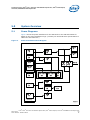
Refer to Figure 1 for complete detailed features of the Intel® Xeon® Processor with 800
MHz system bus and Intel® E7520 and Intel® 6300ESB Customer Reference Board
(CRB).
1.4
Block Diagram
Figure 1.
Customer Reference Board Block Diagram
®
®
ITP
Intel
Xeon
Intel
Xeon
PCI-X
133 MHz
PCI-E
PXH
DDR2 400
®
P CI-X 100M Hz
PCI-E
Intel
E7520
M CH
DDR
DDR2
266
400
PCI-E x4
CK409B
PCI-X 66MHz
PCI-E x8
DB800
LM 93
HI 1.5
IDE
PCI-X
®
Intel
6300ESB
ICH
PCI
PCI 33M Hz
IDE
S-ATA
VG A
S-ATA
UART 1
USB 2.0
UART 2
USB 2.0
Floppy
USB 2.0
SIO
USB 2.0
P arallel
FW H
P S2
LPC Debug
UART 3
Intel® Xeon® Processor with 800 MHz System Bus, Intel® E7520 Chipset, and Intel® 6300ESB ICH Development Kit
UG
March 2007
8
Order Number: 300281-006US
Product Overview—Intel® Xeon™ Processor with 800 MHz System Bus, Intel® E7520 Chipset,
and Intel® 6300ESB ICH Development Kit
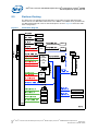
Figure 2.
Placement—Top View
2' ( 2 '1
PXH
!%
!
3
2' 2 '1
2' 2 '1
!("(
&'
!("(
. /+! 0% 2 // '1
. /+! 0% 2 // '1
+,-- ,
Intel®
6300ESB
I/O
Controller
!! $
+,-- ,
)*
. /+! 0%
'1
4
MCH
!! # +
+
!
!0
!
"2
""
+
3"
Intel® Xeon® Processor with 800 MHz System Bus, Intel® E7520 Chipset, and Intel ® 6300ESB ICH Development Kit
March 2007
UG
Order Number: 300281-006US
9
Intel ® Xeon™ Processor with 800 MHz System Bus, Intel® E7520 Chipset, and Intel® 6300ESB
ICH Development Kit—Product Overview
1.4.1
Memory Subsystem
The memory subsystem is designed to support Double Data Rate2(DDR2) Synchronous
Dynamic Random Access Memory (SDRAM) using the Intel(R) E7520 MCH. The MCH
provides two independent DDR channels, which support DDR2-400 DIMMs. The peak
bandwidth of each DDR2 branch channel is 3.2 Gbyte/s (8 bytes x 400 MT/s) with
DDR2-400. The two DDR2 channels from the MCH operate in lock step; the effective
overall peak bandwidth of the DDR2 memory subsystem is 6.4 Gbyte/s for DDR2-400.
Table 2 shows all DIMM technology supported by the CRB. Other DIMM types are not
supported.
Table 2.
Supported DIMM Module Types
Technology
256 Mbit
512 Mbit
1 Gbit
Organization
SDRAM Chips/DIMM
8 Mbytes x 8 x 4 banks
8
16 Mbytes x 4 x 4 banks
16
16 Mbytes x 8 x 4 banks
8
32 Mbytes x 4 x 4 banks
16
32 Mbytes x 8 x 4 banks
8
64 Mbytes x 4 x 4 banks
16
1.4.2
DIMM Placement DDR2-400
Table 3.
DIMM Placement DDR2-400
DIMM Configuration
DIMM1
DIMM2
1 Single Rank
Empty
Single Rank
1 Dual Rank
Empty
Dual Rank
2 Single Rank
Single Rank
Single Rank
1 Dual Rank, 1 Single Rank
Single Rank
Dual Rank
2 Dual Rank
Dual Rank
Dual Rank
Notes:
1.
Populate DIMMs starting with the sockets farthest away from the MCH (DIMM slots A2 and B2).
2.
When populating both channels, always place identical DIMMs in sockets that have the same
position on channel A and channel B (i.e., DIMM A2 should be identical to DIMM B2).
Intel® Xeon® Processor with 800 MHz System Bus, Intel® E7520 Chipset, and Intel® 6300ESB ICH Development Kit
UG
March 2007
10
Order Number: 300281-006US
Product Overview—Intel® Xeon™ Processor with 800 MHz System Bus, Intel® E7520 Chipset,
and Intel® 6300ESB ICH Development Kit
1.5
Memory Population Rules and Configurations
The system supports two DDR2-400 DIMM slots for Channel A and two DDR2-400
DIMM slots for Channel B. The four slots are interleaved and placed in a row in the
following order: A1, B1, A2, B2, with A1 being closest to the MCH. This design supports
only registered ECC-enabled DIMMs.
When populating both channels, always place identical DIMMs in sockets that have the
same position on Channel A and Channel B (i.e., DIMM A2 should be identical to DIMM
B2).
In addition, single-rank DIMMs should be populated furthest when a combination of
single-rank and double-rank DIMMs are used. This recommendation is based on the
signal integrity requirements of the DDR2 interface.
Figure 3.
DDR2-400 Memory - DIMM Ordering
+
DIMM B2
+
DIMM A2
DIMM B1
DIMM A1
+
MCH
B3519-01
Intel® Xeon® Processor with 800 MHz System Bus, Intel® E7520 Chipset, and Intel ® 6300ESB ICH Development Kit
March 2007
UG
Order Number: 300281-006US
11
Intel ® Xeon™ Processor with 800 MHz System Bus, Intel® E7520 Chipset, and Intel® 6300ESB
ICH Development Kit—Platform Management
2.0
Platform Management
The following sections describe how the system power management operates and how
the different ACPI states are implemented. Platform management involves:
• ACPI implementation specific details
• System monitoring, control and response to thermal, voltage and intrusion events
• BIOS security
2.1
Power Button
The system power button is connected to the I/O controller component. When the
button is pressed, the I/O controller receives the signal and transitions the system to
the proper sleep state as determined by the operating system and software. If the
power button is pressed and held for four seconds, the system powers off (S5 state).
This feature is called power button override and is particularly helpful in case of system
hang and system lock.
2.2
Soft Off
The I/O controller incorporates a SLP_S4 output signal which routes to the power
supply. This signal has register access that allows software to deactivate the power
supply. When SLP_S4 goes active, the power supply cuts main power but keeps 5 V
auxiliary power rails available. 5 V auxiliary voltage is active while the power supply
receives AC power.
2.3
Sleep States Supported
The I/O controller controls the system sleep states. States S0, S1, S3, S4, and S5 are
supported. The platform enters sleep states in response to BIOS, operating system or
user actions. Normally the operating system determines which sleep state to transition
into. However, a four-second power button override event places the system
immediately into S5. When transitioning into a software-invoked sleep state, the I/O
controller attempts to gracefully put the system to sleep by first going into the
processor C2 state.
2.3.1
S0 State
This is the normal operating state, even though there are some power savings modes
in this state using processor Halt and Stop Clock (processor C1 and C2 states). S0
affords the fastest wake-up response time of any sleep state because the system
remains fully powered and memory is intact.
2.3.2
S1 State
This state is entered via a processor Sleep signal from the I/O controller (processor C3
state). The system remains fully powered with memory contents intact but the
processors enter their lowest power state. The operating system disables bus masters
Intel® Xeon® Processor with 800 MHz System Bus, Intel® E7520 Chipset, and Intel® 6300ESB ICH Development Kit
UG
March 2007
12
Order Number: 300281-006US
Platform Management—Intel® Xeon™ Processor with 800 MHz System Bus, Intel® E7520
Chipset, and Intel® 6300ESB ICH Development Kit
for uniprocessor configurations while flushing and invalidating caches before entering
this state in multiprocessor configurations. Wake-up latency is slightly longer in this
state than in S0; however, power savings are improved from S0.
2.3.3
S2 State
This state is not supported.
2.3.4
S3 State
This state is called Suspend to RAM (STR). The system context is maintained in system
DRAM, but power is shut off to non-critical circuits. Memory is retained, and refreshes
continue. All clocks stop except the RTC. S3 is entered when the I/O controller asserts
the SLP_S3# signal to downstream circuitry to control 1.8 V power plane switching.
Power must be switched from the normal 1.8 V rail to standby 1.8 V, because the EPS12V 550 W power supply does not directly supply a standby 1.8 V rail. The sequence to
enter Suspend to RAM is as follows:
1. The OS and BIOS prepare for S3 sleep state.
2. The OS sets the appropriate sleep bits in the I/O controller.
3. The I/O controller drives STPCLK to the processors.
4. The processors respond with a Stop-Grant cycle, passed over hub interface by
MCH.
5. The I/O controller indicates an S3 (STR) sleep mode to the MCH via Hub Interface
A.
6. The MCH puts DDR memory into the self-refresh mode.
7. The MCH drives DDR CMDCLK differential pairs and all DDR outputs low.
8. The MCH drives a completion message via Hub Interface A to the I/O controller.
9. The I/O controller turns off all voltage rails (except Standby 5V) from the main
power supply by asserting the SLP_S3_N signal.
— When in the S3 state, only the Standby 5 V rail is available from the power
supply. The board uses this standby source to generate 1.8 V standby rail to
power the DIMMs.
— The asserted SLP_S3_N signal also controls the logic to switch the DIMM power
source from main 1.8 V to standby 1.8 V.
2.3.5
S4 State
This state is called Suspend to Disk. From a hardware perspective, it is equivalent to an
S5 state. The operating system is responsible for saving the system context in a special
partition on the hard drive. Although the system must power up and fully boot, boot
time to an application is reduced because the platform is returned to the same system
state as when the preceding power off occurred.
2.3.6
S5 State
This state is the normal off state whether entered through the Power Button or Soft Off.
All power is shut off except for the logic required to restart. The system remains in the
S5 State only while the power supply is plugged into the electrical outlet. If the power
supply is unplugged, this is considered a Mechanical OFF or G3.
Intel® Xeon® Processor with 800 MHz System Bus, Intel® E7520 Chipset, and Intel ® 6300ESB ICH Development Kit
March 2007
UG
Order Number: 300281-006US
13
Intel ® Xeon™ Processor with 800 MHz System Bus, Intel® E7520 Chipset, and Intel® 6300ESB
ICH Development Kit—Platform Management
2.3.7
Wake-Up Events
The types of wake-up events and wake-up latencies are related to the actual power
rails available to the system in a particular sleep state, as well as to the location in
which the system context is stored. Regardless of the Sleep State, Wake on the Power
Button is always supported except in a mechanical off situation. When in a Sleep State,
the system complies with the PCI specification by supplying the optional 3.3 V standby
voltage to each PCI slot as well as the PME# signal. This enables any compliant PCI
card to wake up the system from supported sleep states except Mechanical Off.
Note:
Wake on USB, Wake on PS/2, and Wake on LAN are not supported.
2.3.8
Wake-Up from S1 Sleep State
During S1, the system is fully powered, permitting support for PCI Express* Wake and
Wake on PCI PME#.
2.3.9
Wake-Up from S4 and S5 States
The power button is used to wake from S4 and S5.
2.4
PCI PM Support
This design holds the system reset signal low when in a sleep state. The system
supports the PCI PME# signal and provides 3.3 V standby to the PCI and PCI Express
slots. This support allows any compliant PCI or PCI Express card to wake up the system
from any sleep state except mechanical off. The user and the operating system must
configure the system carefully following the PCI power management interface
specification because of the limited amount of power available on 3.3 V standby.
2.5
Platform Management
The LM 93 monitors the majority of the system voltages. The VID signals from the
processors are also monitored by LM 93. All voltage levels can be read via the SMBus.
2.5.1
Processor Thermal Management
Each processor monitors its own core temperature and thermally manages itself when
it reaches a certain temperature. The system also uses the internal processor diode to
monitor the die temperature. The diode pins are routed to the diode input pins in the
LM 93. The LM 93 can be programmed to force the processor fans to full speed
operation when it senses the processor core temperature exceeding a specific value. In
addition, the LM 93 has an on chip thermal monitor which allows it to monitor the
incoming ambient temperature. Additional processor thermal management requires the
system to communicate to the processors when the VRD reaches a critical
temperature. The VR thermal monitor asserts FORCEPR_N signal to the processor. The
thermal monitor, an LM26, is a ±3° C precision thermostat used to sense high
temperature conditions and drive a digital output active low. This circuit works as an
external PROCHOT event to further protect the processor during high current/
temperature conditions. This forces the processor to activate a thermal protection
circuit that reduces the current consumption of the processor.
2.6
System Fan Operation
The system uses both the LM 93 and the National* 87427 Super I/O to monitor and
control the fans in the system.The LM93 uses pulse width modulated (PWM) outputs
that can modulate the voltage across the fans, providing a variable duty cycle to effect
Intel® Xeon® Processor with 800 MHz System Bus, Intel® E7520 Chipset, and Intel® 6300ESB ICH Development Kit
UG
March 2007
14
Order Number: 300281-006US
Platform Management—Intel® Xeon™ Processor with 800 MHz System Bus, Intel® E7520
Chipset, and Intel® 6300ESB ICH Development Kit
a reduced DC voltage from nominal 12 VDC. The fan headers are the standard 12V,
three-pin type, used in previous Servers, which support tachometer out. The LM 93
also has four tachometer inputs that it can use to monitor the fans that it is controlling.
All fan tachometer data can be extracted from the controllers via the SMBus. The
system fan speed control circuit does not control the power supply fan. Each PWM
output has a bypass jumper that causes all fans to run at full speed and ignore the
PWM control. Each processor fan has its own dedicated PWM output and tachometer
input, so each fan is controlled and monitored independently, depending on the core
temperature. The LM 93 is dedicated to processor fan speed control and monitor, and
can be programmed with temperature limit values that allow it to speed up or idle the
processor fans, depending upon the input temperature.
Intel® Xeon® Processor with 800 MHz System Bus, Intel® E7520 Chipset, and Intel ® 6300ESB ICH Development Kit
March 2007
UG
Order Number: 300281-006US
15
Intel ® Xeon™ Processor with 800 MHz System Bus, Intel® E7520 Chipset, and Intel® 6300ESB
ICH Development Kit—Equipment Required for CRB Usage
3.0
Equipment Required for CRB Usage
The following components are required for the Intel® Xeon® Processor with 800 MHz
System Bus and Intel® E7520 and Intel® 6300ESB Customer Reference Board (CRB)
usage:
• A 460 W SSI EPS 12 V power supply. The CRB is shipped with the power supply.
• At least two modules of DDR2-400 DIMM. The CRB is shipped with two 1 GBytes of
DDR2 400.
• Hard drive loaded with Operating System1
• Monitor
• PS/2 mouse and keyboard
Visually inspect the board and ensure that the MCH, Intel® 6300ESB I/O Controller,
PXH, and other components did not shake loose during shipment. If the board has any
loose or missing components, contact your Intel representative.
Caution:
Powering up without all components installed correctly could lead to a power-up failure
that could damage the board. Do not power up the board until the source of any loose
component is determined and the component has been replaced on the board.
3.1
Precautions
Warning:
Do not install the power supply until all other installation steps have been completed.
Measures must be taken to protect the unused DC connectors of the power supply from
accidental contact to objects in the work area.
Note:
Review the document provided with the Development Kit titled “Important Safety and
Regulatory Information”. This document contains addition safety warnings and cautions
that must be observed when using this development kit.
The following precautions will reduce the chances of damaging the board:
• Ensure that a 460 W SSI EPV 12 V power supply is used to power up the CRB. Refer
to Section 5.1, “Power Diagrams” on page 25 for details on the SSI power supply
interface on the CRB.
• This platform supports DDR2-400 DIMMs; ensure that the same speed DIMM is
plugged in all slots of the platform.
• Ensure that each processor has heat sinks attached before powering up the board.
• Ensure that the heat sink is attached to the MCH and PXH before powering up the
board. Never attach a heat sink while the board is powered.
• Use Table 4 to verify that all jumpers are in their default positions.
1. Note The hard disk provided with the development kit is not pre-loaded with any software.
Intel® Xeon® Processor with 800 MHz System Bus, Intel® E7520 Chipset, and Intel® 6300ESB ICH Development Kit
UG
March 2007
16
Order Number: 300281-006US
Equipment Required for CRB Usage—Intel® Xeon™ Processor with 800 MHz System Bus, Intel®
E7520 Chipset, and Intel® 6300ESB ICH Development Kit
3.2
Driver and OS Requirements
The required INF driver for the CRB supports the functionality of the Intel® 6300ESB I/
O Controller and PXH. The INF file will be included with Red Hat* compatible drivers on
the CD shipped with the kit.
The CRB supports these operating systems:
• Microsoft* Windows* XP, Windows Embedded XP, 2000 Pro, 2000 Server, 2000
Advanced Server, 2003 Standard Edition
• Red Hat Linux Advanced Server 2.1, Red Hat 8.0 on kernel 2.4.x
• Wind River* VxWorks* real-time operating system
• QNX Neutrino* real-time operating system
• Customer operating systems when applicable
3.2.1
Drivers Included on CD
3.2.1.1
Red Hat 8.0 Compatible Driver Package Contents
This operating system compatible driver package is available from:
http://downloadfinder.intel.com/scripts-df/
Detail_Desc.asp?agr=Y&ProductID=1706&DwnldID=7249
Package Contents
esb_rh8.txt — release notes
sources/ac97/alsa-driver-0.9.0rc5.bz2— alsa-driver sources
sources/ac97/alsa-lib-0.9.0rc5.bz2— alsa-lib sources
sources/ac97/alsa-util-0.9.0rc5.bz2— alsa-util sources
sources/ac97/alsa-xmms-0.9.9b.tar.gz— alsa plugin for xmms
sources/ac97/xmms-mpg123-1.2.7-13.i386.rpm— mpeg plugin for xmms
sources/kernel/linux-2.4.20.tar.gz— 2.4.20 kernel sources
sources/kernel/config-2.4.20-p4-upapic-i2c-apm-nooss— UP Kernel Config
File
sources/kernel/config-2.4.20-p4-upapic-i2c-acpi-nooss— UP Kernel Config
File
sources/kernel/config-2.4.20-p4-smp-i2c-apm-nooss— MP Kernel Config
File
sources/smbus/i2c-2.7.0.tar.gz— latest I2C-core driver sources
sources/smbus/lm_sensors-2.7.0.tar.gz— latest smbus adapter/sensor
sources
sources/esbwdt/LICENSE— license for Intel WDT driver
sources/esbwdt/esbwdt-doc.txt— Linux WDT Driver release notes
sources/esbwdt/driver/esbwdt.c— Linux WDT Driver source file
sources/esbwdt/driver/esbwdt.h— Linux WDT Driver header file
sources/esbwdt/driver/Makefile— Linux WDT Driver Makefile
sources/esbwdt/demoapp/esbwdt-demo.c— WDT driver demo application
patches/COPYING— GPL-v2 license for Intel patches
patches/ac97/alsa-hr.patch— enables ESB AC97 AC in ALSA
patches/ac97/alsa-hr-ich5.patch— enables ICH5 AC97 AC in ALSA
patches/ide-sata/pci_ids-hr.patch— enables ICH5 AC97 AC in ALSA
patches/ide-sata/pci_ids-hr-ich5.patch— patches to 2.4.20 IDE driver
Intel® Xeon® Processor with 800 MHz System Bus, Intel® E7520 Chipset, and Intel ® 6300ESB ICH Development Kit
March 2007
UG
Order Number: 300281-006US
17
Intel ® Xeon™ Processor with 800 MHz System Bus, Intel® E7520 Chipset, and Intel® 6300ESB
ICH Development Kit—Equipment Required for CRB Usage
patches/ide-sata/piix.c-hr.patch— enables PATA & SATA storage interface
support
patches/ide-sata/piix.c-hr-ich5.patch— enables PATA & SATA storage interface
support
patches/ide-sata/ide_pci-hr.patch— integrated into the ESB & ICH5
Southbridges
patches/ide-sata/ide_pci-hr-ich5.patch— integrated into the ESB & ICH5
Southbridges
patches/ide-sata/pci_irq-hr.patch— integrated into the ESB & ICH5
Southbridges
patches/ide-sata/pci_irq-hr-ich5.patch— integrated into the ESB & ICH5
Southbridges
patches/lspci/pciids-112202.patch— patch to update 2.4.20 pci.ids file
patches/lspci/pciids-112202-hr.patch— patch to add ESB dev IDs to pci.ids
patches/lspci/pciids-112202-hr-ich5.patch— patch to add ICH5 dev IDs to
pci.ids
patches/ioapic/irqbalance-2.4.20-MRC.patch— patch for use with P4 HyperThreading
patches/smbus/i2c-hr.patch— enables ESB SMBUS dev in I2C driver
patches/smbus/i2c-hr-ich5.patch — enables ICH5 SMBUS dev in I2C driver
patches/smbus/i2c-2.7.0-Makefile.patch — customizations for I2C-2.7.0
Makefile
patches/smbus/lm_sensors-2.7.0-Makefile.patch — customizations for
lm_sensors Makefile
patches/smbus/readme.txt— build/install instruction for lm_sensors
binaries/binaries.tar.gz — pre-build kernel and modules
utils/ks.cfg-raid015-hd-acd — raid0, 1, & 5 enabled kickstart file
utils/ks.cfg-noraid-hda — non-RAID kickstart file
utils/debug/readme-up.txt — instructions on using UP install scripts
ks.cfg-noraid-hda-cdrom-text-interactive— interactive kickstart file
install-bin.pl— script to automate UP pkg install
bldsrcs.pl — script to automate UP pkg install
readme-smp.txt— instructions on using SMP install scripts
bldsmpkernel.pl— script to automate SMP kernel bld/install
bldsmpdrivers.pl— script to automate SMP driver modules bld
3.2.1.2
Red Hat Advanced Server 2.1 Compatible Driver Package Contents
This operating system compatible driver package is available from:
http://downloadfinder.intel.com/scripts-df/
Detail_Desc.asp?agr=Y&ProductID=1706&DwnldID=7248
Package Contents
esb_rhas.txt— release notes
sources/ac97/alsa-driver-0.9.0rc5.bz2— alsa-driver sources
sources/ac97/alsa-lib-0.9.0rc5.bz2— alsa-lib sources
sources/ac97/alsa-util-0.9.0rc5.bz2— alsa-util sources
sources/ac97/alsa-xmms-0.9.9b.tar.gz— alsa plugin for xmms
sources/ac97/README— build/install instructions for ac97
sources/kernel/config-2.4.9-e.24-p4-smp-i2c— Optimized MP Kernel Config
File
sources/kernel/config-2.4.9-e.24-p4-upapic-i2c— Optimized UP Kernel
Config File
Intel® Xeon® Processor with 800 MHz System Bus, Intel® E7520 Chipset, and Intel® 6300ESB ICH Development Kit
UG
March 2007
18
Order Number: 300281-006US
Equipment Required for CRB Usage—Intel® Xeon™ Processor with 800 MHz System Bus, Intel®
E7520 Chipset, and Intel® 6300ESB ICH Development Kit
sources/kernel/install-2.4.9-e.24esb-grub.conf.patch— Patch to install UP
kernel
sources/kernel/install-2.4.9-e.24esbsmp.patch— Patch to install SMP kernel
sources/kernel/rhas21-q2u-gold-iso— origin of RHAS Q2-03 updates
sources/smbus/i2c-2.7.0.tar.gz— latest i2c-core driver sources
sources/smbus/lm_sensors-2.7.0.tar.gz— latest smbus adapter/sensor
sources
sources/esbwdt/LICENSE — license for Intel WDT driver
sources/esbwdt/esbwdt-doc.txt— esbwdt driver/demoapp release notes
sources/esbwdt/driver/esbwdt.c— esbwdt driver sources
sources/esbwdt/driver/esbwdt.h— esbwdt driver header file
sources/esbwdt/driver/Makefile— esbwdt driver Makefile
sources/esbwdt/demoapp/esbwdt-demo.c— esbwdt driver demo app
patches/COPYING— GPL-v2 license for Intel patches
patches/ac97/alsa-hr.patch— enables ESB AC97 AC in alsa
patches/ac97/alsa-hr-ich5.patch— enables ICH5 AC97 AC in alsa
patches/ide-sata/pci_ids-hr.patch— patches to 2.4.9-e.24 ide driver
patches/ide-sata/pci_ids-hr-ich5.patch— patches to 2.4.9-e.24 ide driver
patches/ide-sata/piix.c-hr.patch— to enable support for pata & sata storage
interfaces
patches/ide-sata/piix.c-hr-ich5.patch— to enable support for pata & sata
storage interfaces
patches/ide-sata/ide_pci-hr.patch— integrated into the esb6300 & ich5
southbridges
patches/ide-sata/ide_pci-hr-ich5.patch— integrated into the esb6300 & ich5
southbridges
patches/ide-sata/pci_irq-hr.patch— integrated into the esb6300 & ich5
southbridges
patches/ide-sata/pci_irq-hr-ich5.patch— integrated into the esb6300 & ich5
southbridges
patches/lspci/pci.ids-hr.patch— adds esb dev ids to 2.4.9-e.24 pci.ids
patches/lspci/pci.ids-hr-ich5.patch— adds ich5 dev ids to 2.4.9-e.24 pci.ids
patches/smbus/i2c-hr.patch— enables esb smbus dev in i2c driver
patches/smbus/i2c-hr-ich5.patch— enables ich5 smbus dev in i2c driver
patches/smbus/i2c-2.7.0-Makefile.patch— customizations for i2c-2.7.0
Makefile
patches/smbus/lm_sensors-2.7.0-Makefile.patch— customizations for
lm_sensors Makefile
sources/smbus/lm_sensors-2.7.0-Module.mk-patch— patch to fix bld errs
on rhas v21
patches/smbus/readme.txt — build/install instructions for smbus
utils/debug/ks.cfg-yyyy— basic kickstart file to install from ftp to hda
utils/debug/bldkernel.pl— script to build/install esb enabled UP kernel
utils/debug/bldsrcs.pl— script to build/install esb enabled UP drivers
utils/debug/readme.txt— BKM (aka EASIEST) way to install UP kernel & drivers
utils/debug/bldsmpkern.pl— script to build/install esb enabled SMP kernel
utils/debug/bldsmpdrivers.pl— script to build/install esb enabled SMP drivers
utils/debug/readme-smp.txt— BKM (aka EASIEST) way to install SMP kernel &
drivers
3.2.1.3
Windows Compatible Driver Package Contents
This operating system compatible driver package is available from:
Intel® Xeon® Processor with 800 MHz System Bus, Intel® E7520 Chipset, and Intel ® 6300ESB ICH Development Kit
March 2007
UG
Order Number: 300281-006US
19
Intel ® Xeon™ Processor with 800 MHz System Bus, Intel® E7520 Chipset, and Intel® 6300ESB
ICH Development Kit—Equipment Required for CRB Usage
http://downloadfinder.intel.com/scripts-df/
Detail_Desc.asp?agr=Y&ProductID=1706&DwnldID=7246
Package Contents
ESB_windows_Relnotes.txt— Release notes for Windows* compatible drivers
SMB.SYS— SMBus Driver
SMB.INF— Install file for SMBus driver
SMB.CAT— SMBus driver security catalog file
STAC97.SYS— AC'97 audio code driver provided by SigmaTel*
SLAoemisv1.doc— Single-user and OEM license for SigmaTel STA97 driver
WDTDRVR.SYS— Watchdog Timer driver
WDTDRVR.INF— Install file for Watchdog Timer driver
WDT_LICENSE.TXT— Generic Alpha license for Watchdog Timer components
WDTDEMO.EXE— Demo program for exercising Watchdog Timer features
Mfc42.dll— Microsoft C++ runtime library
Mfco42.dll— Microsoft C++ runtime library
Msvcrtd.dll— Microsoft C++ runtime library
wdtdemoAppSpec.pdf— WdtDemo App user documentation
wdtdriverspec.pdf— Overview of Watchdog Timer driver
Intelwdtapi.pdf— Watchdog Timer driver interface API document
IWDTLIB.DLL— Watchdog Timer Interface Dynamic Link Library
CWESB.slx eXP— Configuration file
WESB.log— log of OS build for eXP
eXP-README.DOC— readme of eXP build
infinst_enu.exe— Intel INF update utility
3.2.1.4
Third Party Drivers
Included on the CD is software compatible with the ATI Rage* Mobility-M Graphics
Accelerator 021112a-006561C-ATI.zip.
Intel® Xeon® Processor with 800 MHz System Bus, Intel® E7520 Chipset, and Intel® 6300ESB ICH Development Kit
UG
March 2007
20
Order Number: 300281-006US
Jumpers and Headers—Intel® Xeon™ Processor with 800 MHz System Bus, Intel® E7520
Chipset, and Intel® 6300ESB ICH Development Kit
4.0
Jumpers and Headers
This section describes the platform component placement as well as configuration, test
and debug features of the Intel® Xeon® Processor with 800 MHz System Bus and
Intel® E7520 and Intel® 6300ESB Customer Reference Board.
4.1
Jumpers
Figure 4 depicts all jumpers on the CRB. Table 4 illustrates the settings and usage of
the jumpers. Review Table 4 and Figure 4 before changing default setting of the
jumpers on the CRB.
Figure 4.
Intel® Xeon® Processor with 800 MHz System Bus and Intel® E7520 and
Intel®
6300ESB Customer Reference Board Jumper
+
+
+
MCH
PXH
Intel®
6300ESB
I/O
Controller
+
Intel® Xeon® Processor with 800 MHz System Bus, Intel® E7520 Chipset, and Intel ® 6300ESB ICH Development Kit
March 2007
UG
Order Number: 300281-006US
21
Intel ® Xeon™ Processor with 800 MHz System Bus, Intel® E7520 Chipset, and Intel® 6300ESB
ICH Development Kit—Jumpers and Headers
Table 4.
Jumper Settings (Sheet 1 of 3)
Ref Des
3.3V Aux Enable
J1A1
Enables 3.3 V AUX
1-2: Enable 3.3 V AUX for wake events
Open: 3.3 V Operation Only
1-2
Enable PXH
J2G2
Enable PXH
1-2: Enable
Open: Disable
1-2
No Reboot
J2G3
Prevents the system from rebooting following
a reset from Intel 6300ESB I/O Controller
1-2: No Reboot
Open: Normal
Enable Super I/O Chip
J2J1
Enable on SIO
1-2: Enable
Open: Disable
1-2
5V Aux Enable
J3A1
Enables 5 V AUX
1-2: Enable 5 V VAUX for wake events
Open: 3.3 V Operation Only
1-2
CPU0 Present Override
J2H114
Enable Video
J4A1
Enable on Board video
1-2: Enable
Open: Disable
J3J1
LED Control
1-2 : Illuminate LED CR4J1 when EDT expires
1-2
J3J2
Reset Control
1-2 : Reset board when WDT Expires
1-2
ICH VSWING Header
J4G5
Access to ICH VSWING pin
Do not Install Jumper
Open
ICH VREF Header
J4G6
Access to ICH VREF pin
Do not Install Jumper
Open
J4H1
Access to PCI SMbus
Do not install Jumper
1: PCI _SMBDAT
2. Ground
3. PCI_SMBCLK
Open
J4H3
Access to DDR SMbus
Do not install Jumper
1: DIMM _SMBDAT
2. Ground
3. DIMM_SMBCLK
Open
ICH WDT Output
PCI SMBus Header
DDR SMBus Header
Description/Settings
Default
Position
Jumper Name
Override VRM disable if no CPU0 installed
1-2 Override
Open : Normal
BSEL0
FSB Clock Frequency Override
(Host Clock Jumpers)
BSEL1: J4H4
BSEL0: J4J3
BSEL1
Open
Open
1-2
(not
populated)
SPEED
1-2
1-2
Normal
2-3
2-3
RSVD
2-3
Open
133 MHz
Open
Open
167 MHz
Open
1-2
200 MHz
BSEL0: 1-2
BSEL1: 1-2
Intel® Xeon® Processor with 800 MHz System Bus, Intel® E7520 Chipset, and Intel® 6300ESB ICH Development Kit
UG
March 2007
22
Order Number: 300281-006US
Jumpers and Headers—Intel® Xeon™ Processor with 800 MHz System Bus, Intel® E7520
Chipset, and Intel® 6300ESB ICH Development Kit
Table 4.
Jumper Settings (Sheet 2 of 3)
Ref Des
SMI Inject
J4H5
Inject SMI Signal
Do Not Install Jumper
Open
FORCEPR0 inject
J4H6
Inject FORCEPR0 Signal
Do Not Install Jumper
Open
STPCLK Inject
J4J1
Inject STPCLK Signal
Do Not Install Jumper
Open
FORCEPR1 inject
J4J2
Inject FORCEPR1 Signal
Do Not Install Jumper
Open
CPU1 Present Override
J4J5
Override VRM disable if CPU1 is not present
1-2: Override
Open: Normal
Open
BSEL Match Override
J4J7
Override VRM disable if BSELs do not match
1-2: Override
Open: Normal
Open
CPU1 VID
J4K1
1-2: VID[5]
3-4: VID[4]
5-6: VID[3]
7-8: VID[2]
9-10: VID[1]
11-12: VID[0]
CPU1 VID Override
J4K2
Manual VID select
1-2: Manual select
Open: CPU select
Open
MCH SMBus Header
J5D3
Access to MCH SMbus
Do not install Jumper
1: MCH _SMBDAT
2. Ground
3. MCH_SMBCLK
Open
PLLS0
J5E112
See MCH Documentation for alternative Gear
Ratios for MCH FSB/Memory
Short
Intel 6300ESB I/O
Controller Top Swap (FWH
Memory Swap)
J5F1
Intel 6300ESB I/O Controller Top Swap
1-2: Top Swap
Open: Normal
Open
PLLS1
J5F113
See MCH Documentation for alternative Gear
Ratios for MCH FSB/Memory
Short
Intel 6300ESB I/O Controller
Safe Mode
J5F3
Intel 6300ESB I/O Controller Safe Mode
1-2: Safe Mode
Open: Normal Mode
Open
CMOS Clear
J5H1
Clears CMOS
1-2: Normal
2-3: Configure
Validation Only
J5H2
Validation only
Do Not Install Jumper
Open
ICH SMBUS header
J5H3
Access to ICH SMBus
Do not Install Jumper
1: ICH_SMBDAT
2. Ground
3. ICH_SMBCLK
Open
S3 Enable
J7F1
1-2: S3 Enable
Open S3 Disable
®
Description/Settings
Default
Position
Jumper Name
As Required
1-2
1-2
Intel® Xeon® Processor with 800 MHz System Bus, Intel® E7520 Chipset, and Intel ® 6300ESB ICH Development Kit
March 2007
UG
Order Number: 300281-006US
23
Intel ® Xeon™ Processor with 800 MHz System Bus, Intel® E7520 Chipset, and Intel® 6300ESB
ICH Development Kit—Jumpers and Headers
Table 4.
Jumper Settings (Sheet 3 of 3)
Ref Des
CPU1 Fan Override
J7K1
1-2: Full Speed
Open: LM93 Controlled
1-2
CPU0 Fan Override
J8J1
1-2: Full Speed
Open: LM93 Controlled
1-2
ITP Configuration
J9 G4
J9G3
2-2: Uniprocessor
1-2: Dual Processor
1-2
1-2
CPU0 Boot Select
J9H2
1-2: Other processor support (RSVD)
Open: Intel Xeon support
Open
CPU0 VID Override
J9K1
Manual VID select
1-2: Manual select
Open: CPU select
Open
J9K2
1-2: VID[5]
3-4: VID[4]
5-6: VID[3]
7-8: VID[2]
9-10: VID[1]
11-12: VID[0]
CPU0 VID
Description/Settings
Default
Position
Jumper Name
As Required
Intel® Xeon® Processor with 800 MHz System Bus, Intel® E7520 Chipset, and Intel® 6300ESB ICH Development Kit
UG
March 2007
24
Order Number: 300281-006US
System Overview—Intel® Xeon™ Processor with 800 MHz System Bus, Intel® E7520 Chipset,
and Intel® 6300ESB ICH Development Kit
5.0
System Overview
5.1
Power Diagrams
Figure 5 shows the power distribution for the CRB. Refer to the CRB schematics for
details on the power distribution logic. (Contact your Intel field sales representative to
obtain the schematics file.)
Figure 5.
Power Distribution Block Diagram
!!"#
!!"#
May be Shared
VRM 10.1
650WSI
(EPS12V)
Intel® Xeon® Processor with 800 MHz System Bus, Intel® E7520 Chipset, and Intel ® 6300ESB ICH Development Kit
March 2007
UG
Order Number: 300281-006US
25
Intel ® Xeon™ Processor with 800 MHz System Bus, Intel® E7520 Chipset, and Intel® 6300ESB
ICH Development Kit—System Overview
5.2
Platform Clocking
The CRB uses one CK409B Clock Synthesizer to generate the host differential pair
clocks and the 100 MHz differential clock to the DB800. The DB800 then generates the
100 MHz differential pair clock for the PCI Express* devices. Figure 6 shows the CRB
clock configuration.
Clock Block Diagram
CPU0
CPU1
ITP
SMA
MCH
DDRA
DDRB
! %
%
SIO
!!
!"
%
!
PCI-X
"
!
PCI-X
"
Intel
6300ESB
I/O
Controller
Hub
!
% PCI-X
Figure 6.
PXH
HI LAI
!
% #$"
Video
&'
FWH
"
Port 80
!"
PCI 2.2
$
!"(
$
!"
PCI Express Slot
PCI Express Slot
DB800
CK-409
Intel® Xeon® Processor with 800 MHz System Bus, Intel® E7520 Chipset, and Intel® 6300ESB ICH Development Kit
UG
March 2007
26
Order Number: 300281-006US
System Overview—Intel® Xeon™ Processor with 800 MHz System Bus, Intel® E7520 Chipset,
and Intel® 6300ESB ICH Development Kit
5.3
Platform Resets
Figure 7 depicts the reset logic for the CRB. The Intel 6300ESB I/O Controller provides
most of the reset following assertion of power good and system reset. However, the
glue logic within the SIO is also used to buffer reset to PXH, MCH, FWH, and IDE.
Platform Reset Diagram
PCI 32
PCI-X
VRM_PWRGD
PCI-X
FWH
Port 80
MCH
Intel®
6300ESB
I/O
Controller
Hub
IDE
CPU 0
CPURST#
PCIRST_N
SYS_RESET#
IDERST#
PCIRST2#
PCIRST1#
SIO
SYS_PWRGD_3V3
CPU 1
ITP-700
PXH_PBPCIRST_N
PXH
PCI-E
PXH_PAPCIRST_N
Figure 7.
PCI-X
PCI-X
PCI-X
B2938-03
Intel® Xeon® Processor with 800 MHz System Bus, Intel® E7520 Chipset, and Intel ® 6300ESB ICH Development Kit
March 2007
UG
Order Number: 300281-006US
27
Intel ® Xeon™ Processor with 800 MHz System Bus, Intel® E7520 Chipset, and Intel® 6300ESB
ICH Development Kit—System Overview
5.4
SMBus
Figure 8 below illustrates the routing of the SMBus signal among the components.
Figure 8.
SMBus Block Diagram
Intel 6300ESB I/O
Controller Hub
LM 93
SMBus
Repeater
ITP-XDP
SMBus
Master Only
9
CK409B
DB800
PCI-X 100 MHz
Slot (Slot #2)
PCI Express
Slot (Slot #4)
PCI Express
Slot (Slot #5)
SMBus
Repeater
PXH-D
PCI-X 133 MHz
Slot (Slot #1)
PCI-X 100 MHz
Slot (Slot #3)
9
Intel E7520
Chipset
9
DIMM #A1
Addr 0xA0
DIMM #B1
Addr 0xA8
PCI-X 66 MHz
Slot (Slot #6)
PCI-X 66 MHz
Slot (Slot #7)
DIMM #A2
Addr 0xA2
DIMM #B2
Addr 0xAA
DDR CH A
DDR CH B
PCI 32-bit /
33 MHz (Slot #8)
Intel® Xeon® Processor with 800 MHz System Bus, Intel® E7520 Chipset, and Intel® 6300ESB ICH Development Kit
UG
March 2007
28
Order Number: 300281-006US
System Overview—Intel® Xeon™ Processor with 800 MHz System Bus, Intel® E7520 Chipset,
and Intel® 6300ESB ICH Development Kit
5.5
Platform IRQ Routing
Figure 9 shows that the Intel 6300ESB I/O Controller uses these segments:
• IRQ14 and 15 for IDE segment
• SERIRQ for SIOPIXRQ segment
• PCRIRQ for the PCI-X segment
• PIRQ for the PCI 32/33 segment
A Message Signalled Interrupt (MSI) scheme is used between the MCH and PXH over
the PCI Express bus. The PXH uses PAIRQ for the Channel A interface to PCI-X 64-bit/
100 MHz peripherals and PBIRQ for the Channel B interface to PCI-X 64/133. MSI and
Non Maskable Interrupt (NMI) are connected from the Intel 6300ESB I/O Controller to
CPU0 and CPU1. The platform also supports MSI for maskable and non-maskable
interrupts.
IRQ Routing Diagram
PCI-E
8x
MSI
MSI
PCI-X 64/133
PCI-X SLOT
REQ/GNT: 1
IDSEL: AD18
A B C D
PCI-E
HI
PCI-X SLOT
REQ/GNT: 0
IDSEL: AD16
A B C D
SERIRQ
A
B
C
D
E
F
G
H
PCI-X 32/33
PXIRQ
NMI
Intel®
6300ESB
I/O
Controller
Hub
PIRQ
MSI
IRQ14/15
A
B
C
D
PCI-X 64/66
IDE
SMI
SMI
PCI-X SLOT
REQ/GNT: 0
IDSEL: AD17
A B C D
PCI-X 64/100
PCI-E
NMI
CPU0
0
1
2
3
4
5
6
7
PXH
PCI-E
MSI
HI
MSI
MSI
MCH
PCI-E
MSI
MSI
SMI
PAIRQ
MSI
NMI
0
1
2
3
PBIRQ
FSB
FSB
SMI
PCI-X SLOT
REQ/GNT: 0
IDSEL: AD17
A B C D
PCI-X 2.0
PCI-E
4x
MSI
CPU0
NMI
MSI
Figure 9.
Video
REQ/GNT: 1
IDSEL: AD17
A
PCI-X SLOT
REQ/GNT: 0
IDSEL: AD17
A B C D
PCI-X SLOT
REQ/GNT: 1
IDSEL: AD18
A B C D
SIO
B2940-02
Intel® Xeon® Processor with 800 MHz System Bus, Intel® E7520 Chipset, and Intel ® 6300ESB ICH Development Kit
March 2007
UG
Order Number: 300281-006US
29
Intel ® Xeon™ Processor with 800 MHz System Bus, Intel® E7520 Chipset, and Intel® 6300ESB
ICH Development Kit—System Overview
5.6
VRD VID Headers
Provides for manual control of the processor core voltage regulator output level(s).
Normally, the processor should be run at its default VID (voltage identification) value as
set during manufacturing. However, in the event the user needs to set a different VID
value from the default value, it can be accomplished through a jumper block found on
the board. Note that these headers are not populated by default.
The CPU 0 VID header is located at J9K2. CPU 1 VID header is located at J4K1. Table 5
provides the VID settings available via the VID headers.
Table 5.
Processor VRD Settings (Sheet 1 of 2)
VID5
VID4
VID3
VID2
VID1
VID0
VCC_MAX
(V)
VID5
VID4
VID3
VID2
VID1
VID0
VCC_MAX
(V)
0
0
1
0
1
0
0.8375
0
1
1
0
1
0
1.2125
1
0
1
0
0
1
0.8500
1
1
1
0
0
1
1.2250
0
0
1
0
0
1
0.8625
0
1
1
0
0
1
1.2375
1
0
1
0
0
0
0.8750
1
1
1
0
0
0
1.2500
0
0
1
0
0
0
0.8875
0
1
1
0
0
0
1.2625
1
0
0
1
1
1
0.9000
1
1
0
1
1
1
1.2750
0
0
0
1
1
1
0.9125
0
1
0
1
1
1
1.2875
1
0
0
1
1
0
0.9250
1
1
0
1
1
0
1.3000
0
0
0
1
1
0
0.9375
0
1
0
1
1
0
1.3125
1
0
0
1
0
1
0.9500
1
1
0
1
0
1
1.3250
0
0
0
1
0
1
0.9625
0
1
0
1
0
1
1.3375
1
0
0
1
0
0
0.9750
1
1
0
1
0
0
1.3500
0
0
0
1
0
0
0.9875
0
1
0
1
0
0
1.3625
1
0
0
0
1
1
1.0000
1
1
0
0
1
1
1.3750
0
0
0
0
1
1
1.0125
0
1
0
0
1
1
1.3875
1
0
0
0
1
0
1.0250
1
1
0
0
1
0
1.400
0
0
0
0
1
0
1.0375
0
1
0
0
1
0
1.4125
1
0
0
0
0
1
1.0500
1
1
0
0
0
1
1.4250
0
0
0
0
0
1
1.0625
0
1
0
0
0
1
1.4375
1
0
0
0
0
0
1.0750
1
1
0
0
0
0
1.4500
0
0
0
0
0
0
1.0875
0
1
0
0
0
0
1.4625
1
1
1
1
1
1
OFF
1
0
1
1
1
1
1.4750
0
1
1
1
1
1
OFF
0
0
1
1
1
1
1.4875
1
1
1
1
1
0
1.1000
1
0
1
1
1
0
1.5000
0
1
1
1
1
0
1.1125
0
0
1
1
1
0
1.5125
Intel® Xeon® Processor with 800 MHz System Bus, Intel® E7520 Chipset, and Intel® 6300ESB ICH Development Kit
UG
March 2007
30
Order Number: 300281-006US
System Overview—Intel® Xeon™ Processor with 800 MHz System Bus, Intel® E7520 Chipset,
and Intel® 6300ESB ICH Development Kit
Table 5.
Processor VRD Settings (Sheet 2 of 2)
1
1
1
1
0
1
1.1250
1
0
1
1
0
1
1.5250
0
1
1
1
0
1
1.1375
0
0
1
1
0
1
1.5375
1
1
1
1
0
0
1.1500
1
0
1
1
0
0
1.5500
0
1
1
1
0
0
1.1625
0
0
1
1
0
0
1.5625
1
1
1
0
1
1
1.1750
1
0
1
0
1
1
1.5750
0
1
1
0
1
1
1.1875
0
0
1
0
1
1
1.5875
1
1
1
0
1
0
1.2000
1
0
1
0
1
0
1.6000
Intel® Xeon® Processor with 800 MHz System Bus, Intel® E7520 Chipset, and Intel ® 6300ESB ICH Development Kit
March 2007
UG
Order Number: 300281-006US
31
Intel ® Xeon™ Processor with 800 MHz System Bus, Intel® E7520 Chipset, and Intel® 6300ESB
ICH Development Kit—System Overview
5.7
Miscellaneous Buttons
Figure 10 below shows the location of the power buttons within the platform.
Figure 10.
Power Buttons
+
+
"
+
#
MCH
Intel
6300ESB
I/O
Controller
®
PXH
!
+
Intel® Xeon® Processor with 800 MHz System Bus, Intel® E7520 Chipset, and Intel® 6300ESB ICH Development Kit
UG
March 2007
32
Order Number: 300281-006US
Debug Procedure—Intel® Xeon™ Processor with 800 MHz System Bus, Intel ® E7520 Chipset,
and Intel® 6300ESB ICH Development Kit
6.0
Debug Procedure
The debug procedures in this section are used to determine baseline functionality for
the Intel® Xeon® Processor with 800 MHz System Bus, Intel® E7520 Chipset, and
Intel® 6300ESB ICH Development Kit. This is a cursory set of tests designed to provide
a level of confidence in the platform operation.
6.1
Level 1 Debug (Port 80/BIOS)
Refer to the steps in Table 6 when debugging a board that does not boot.
Table 6.
Item
Level 1 Debug (Port 80/BIOS)
Test
Pass/Fail Criteria
Cause of Failure
1
Verify “SYSTEM PWRGD” LED
CR2H1: Green
Power Sequence Failure—go immediately to Level 2
debug
2
Is “PCI Reset” LED (decimal on
DS1J2) illuminated?
Decimal on Port 80 display
Red
PCI Reset Stuck—go to Level 3 debug
3
Verify CPURST LED is off
CR7K3: Off
CPU Reset Stuck—go to Level 3 debug
4
Verify Port 80 Posting
Port 80 LEDs are posting
boot codes and stopping
System Hang—Check BIOS go to level 3 debug. Refer to
AMI* BIOS documentation for details. Also refer to
Schematic Page 68, Coord. D5.
5
Check BIOS revision
Latest BIOS installed
Contact your Intel Representative for the latest BIOS
image.
6
Verify default Jumper settings
See default settings
Improper Jumper settings
Intel® Xeon® Processor with 800 MHz System Bus, Intel® E7520 Chipset, and Intel ® 6300ESB ICH Development Kit
March 2007
UG
Order Number: 300281-006US
33
Intel ® Xeon™ Processor with 800 MHz System Bus, Intel® E7520 Chipset, and Intel® 6300ESB
ICH Development Kit—Debug Procedure
6.2
Level 2 Debug (Power Sequence)
Check the items in Table 7 below if “SYSTEM PWRGD” is not illuminated.
Table 7.
Level 2 Debug (Power Sequence)
Item
Test
Pass/Fail Criteria
Cause of Failure
1
Primary power supply voltages
Measure voltage across:
• C3K2: 3.3 V
• C3K1: -12 V
• C4K3: 5 V
• C4K2: 5 V
• C4K5: 12 V
2
1.8 V
C9E14: 1.8 V
DDR2 power supply failure
3
1.5 V
C5C5: 1.5 V
MCH/PXH/ICH core power supply failure
4
1.8 VSBY
C9G5: 1.8 V
DDR2 standby power supply failure
5
CPU VTT power supply
C9H10: 1.2 V
CPU_VTT power supply failure
6
CPU0 VRD
L9J2: 1.2 V - 1.4 V
CPU0 VRD Failure
7
CPU1 VRD
L5J1: 1.2 V – 1.4 V
CPU1 VRD Failure
8
Verify “SYSTEM PWRGD” LED
CR2H1: Green
Power Sequence Failure
6.3
External power supply failure
Level 3 Debug (Voltage References)
Table 8 includes the first items to look at when debugging a board that does not boot.
Table 8.
Level 3 Debug (Voltage References)
Item
Test
Pass/Fail Criteria
R6D4: 0.9 V
Cause of Failure
1
MCH DDR2 Channel A Vref
Vref incorrect: check resistor values
2
MCHDDR2 Channel B Vref
R6B3: 0.9 V
Vref incorrect: check resistor values
3
MCH Hublink Vref
R5F11: 0.354 V
Vref incorrect: check resistor values
4
MCH Hublink Vswing
R5F8: 0.804 V
Vswing incorrect: check resistor values
5
ICH Hublink Vref
R4G7: 0.347 V
Vref incorrect: check resistor values
6
ICH Hublink Vswing
R4G4: 0.696 V
Vswing incorrect: check resistor values
7
CPU0 VTT Vref
(Back side of board)
R2U5: 0.775 V
R2V2: 0.775 V
Vref incorrect: check resistor values
8
CPU1 VTT Vref
(Back side of board)
R4U5: 0.754
R5V1: 0.754
Vref incorrect: check resistor values
9
MCH VTT Vref
R6F2: 0.775 V
Vref incorrect: check resistor values
10
DIMM A DDR2 Vref
R3M1: 0.9 V
Vref incorrect: check resistor values
11
DIMM B DDR2 Vref
R2M1: 0.9 V
Vref incorrect: check resistor values
Intel® Xeon® Processor with 800 MHz System Bus, Intel® E7520 Chipset, and Intel® 6300ESB ICH Development Kit
UG
March 2007
34
Order Number: 300281-006US
Heatsink Assembly—Intel ® Xeon™ Processor with 800 MHz System Bus, Intel® E7520 Chipset,
and Intel® 6300ESB ICH Development Kit
7.0
Heatsink Assembly
This section provides heatsink assembly instructions for the Intel® Xeon® Processor
with 800 MHz System Bus, Intel® E7520 Chipset, and Intel® 6300ESB ICH
Development Kit:
Components requiring post-secondary heat sink assembly are listed in Table 9.
Table 9.
Components Requiring Heat Sink Assembly
Component
Processors
(See Figure 11.)
Figure 11.
Quantity
per Board
Up to 2
Heat Sink
Manufacturer
Cooler Master
Part Number
Comments
E3W-N73CS-I1
Active heat sink + back plate.
Components Requiring Heat Sink Assembly
Processors
(2)
Intel® Xeon® Processor with 800 MHz System Bus, Intel® E7520 Chipset, and Intel ® 6300ESB ICH Development Kit
March 2007
UG
Order Number: 300281-006US
35
Intel ® Xeon™ Processor with 800 MHz System Bus, Intel® E7520 Chipset, and Intel® 6300ESB
ICH Development Kit—Heatsink Assembly
7.1
Processor Heat Sink Installation Instructions
Note:
Tools/items needed include Phillips screwdriver, disposable towels, and isopropyl
alcohol.
1. Ensure the processor is firmly seated in the socket and the socket latch is closed.
(See Figure 12.)
Figure 12.
Inserting Processor in Socket
2. Clean the processor’s top surface with a clean towel and isopropyl alcohol. (See
Figure 13.)
Intel® Xeon® Processor with 800 MHz System Bus, Intel® E7520 Chipset, and Intel® 6300ESB ICH Development Kit
UG
March 2007
36
Order Number: 300281-006US
Heatsink Assembly—Intel ® Xeon™ Processor with 800 MHz System Bus, Intel® E7520 Chipset,
and Intel® 6300ESB ICH Development Kit
Figure 13.
Cleaning the Processor Surface
3. Insert the processor heat sink back plate into the four mounting holes near the
processor. The back plate is assembled to the back side of the PCB. (See
Figure 14.)
Figure 14.
Installing the Processor Backplate
Intel® Xeon® Processor with 800 MHz System Bus, Intel® E7520 Chipset, and Intel ® 6300ESB ICH Development Kit
March 2007
UG
Order Number: 300281-006US
37
Intel ® Xeon™ Processor with 800 MHz System Bus, Intel® E7520 Chipset, and Intel® 6300ESB
ICH Development Kit—Heatsink Assembly
4. Remove the protective covers from the processor heat sink. There is a cover that
protects the fan, and another that protects the preapplied thermal interface
material on the bottom of the heat sink base. (See Figure 15.)
Figure 15.
Removing the Protective Covers
Remove
plastic
5. Place the heat sink on top of the CPU and align the four screws to the threads of
the backplate.
Figure 16.
Installing the Heatsink
Tighten screw 1
Tighten screw 4
Tighten screw 2
Tighten screw 3
Intel® Xeon® Processor with 800 MHz System Bus, Intel® E7520 Chipset, and Intel® 6300ESB ICH Development Kit
UG
March 2007
38
Order Number: 300281-006US
Heatsink Assembly—Intel ® Xeon™ Processor with 800 MHz System Bus, Intel® E7520 Chipset,
and Intel® 6300ESB ICH Development Kit
6. Using a Phillips screwdriver, tighten the screws in the pattern indicated in
Figure 16. The screws are shoulder screws and will stop threading once completely
tightened.
7. Plug the fan connector into the nearest fan connector on the PCB.
8. If applicable, repeat this process for the second processor.
Intel® Xeon® Processor with 800 MHz System Bus, Intel® E7520 Chipset, and Intel ® 6300ESB ICH Development Kit
March 2007
UG
Order Number: 300281-006US
39