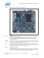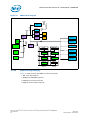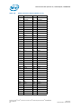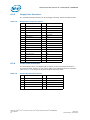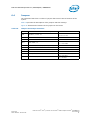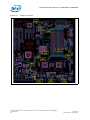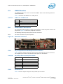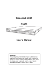
1
Dual-Core Intel® Xeon® processor LV
with Intel® E7520 Chipset and Intel®
6300ESB ICH Development Kit
User’s Manual
April 2007
Order Number: 311274-009
INFORMATION IN THIS DOCUMENT IS PROVIDED IN CONNECTION WITH INTEL® PRODUCTS. NO LICENSE, EXPRESS OR IMPLIED, BY ESTOPPEL OR
OTHERWISE, TO ANY INTELLECTUAL PROPERTY RIGHTS IS GRANTED BY THIS DOCUMENT. EXCEPT AS PROVIDED IN INTEL'S TERMS AND CONDITIONS
OF SALE FOR SUCH PRODUCTS, INTEL ASSUMES NO LIABILITY WHATSOEVER, AND INTEL DISCLAIMS ANY EXPRESS OR IMPLIED WARRANTY, RELATING
TO SALE AND/OR USE OF INTEL PRODUCTS INCLUDING LIABILITY OR WARRANTIES RELATING TO FITNESS FOR A PARTICULAR PURPOSE,
MERCHANTABILITY, OR INFRINGEMENT OF ANY PATENT, COPYRIGHT OR OTHER INTELLECTUAL PROPERTY RIGHT. Intel products are not intended for
use in medical, life saving, life sustaining, critical control or safety systems, or in nuclear facility applications.
Leg al Li nes and Dis clai mers
Intel may make changes to specifications and product descriptions at any time, without notice.
Intel Corporation may have patents or pending patent applications, trademarks, copyrights, or other intellectual property rights that relate to the
presented subject matter. The furnishing of documents and other materials and information does not provide any license, express or implied, by estoppel
or otherwise, to any such patents, trademarks, copyrights, or other intellectual property rights.
Designers must not rely on the absence or characteristics of any features or instructions marked “reserved” or “undefined.” Intel reserves these for
future definition and shall have no responsibility whatsoever for conflicts or incompatibilities arising from future changes to them.
Intel processor numbers are not a measure of performance. Processor numbers differentiate features within each processor family, not across different
processor families. See http://www.intel.com/products/processor_number for details.
The Dual-Core Intel® Xeon® processor LV with Intel® E7520 Chipset and Intel® 6300ESB ICH may contain design defects or errors known as errata
which may cause the product to deviate from published specifications. Current characterized errata are available on request.
Hyper-Threading Technology requires a computer system with an Intel® Pentium® 4 processor supporting HT Technology and a HT Technology enabled
chipset, BIOS and operating system. Performance will vary depending on the specific hardware and software you use. See http://www.intel.com/
products/ht/Hyperthreading_more.htm for additional information.
This User’s Manual as well as the software described in it is furnished under license and may only be used or copied in accordance with the terms of the
license. The information in this manual is furnished for informational use only, is subject to change without notice, and should not be construed as a
commitment by Intel Corporation. Intel Corporation assumes no responsibility or liability for any errors or inaccuracies that may appear in this document
or any software that may be provided in association with this document.
Except as permitted by such license, no part of this document may be reproduced, stored in a retrieval system, or transmitted in any form or by any
means without the express written consent of Intel Corporation.
Contact your local Intel sales office or your distributor to obtain the latest specifications and before placing your product order.
Copies of documents which have an order number and are referenced in this document, or other Intel literature may be obtained by calling
1-800-548-4725 or by visiting Intel's website at http://www.intel.com.
Celeron, Intel, Intel Centrino, Intel logo, Intel NetBurst, Intel NetStructure, Intel Xeon, Intel XScale, Pentium, Pentium II Xeon, Pentium III Xeon and
VTune are trademarks or registered trademarks of Intel Corporation or its subsidiaries in the United States and other countries.
*Other names and brands may be claimed as the property of others.
Copyright © 2007, Intel Corporation. All Rights Reserved.
Dual-Core Intel® Xeon® processor LV with Intel® E7520 Chipset and Intel® 6300ESB ICH
User’s Manual
2
April 2007
Order Number: 311274-009
Dual-Core Intel Xeon processor LV / E7520 Chipset / 6300ESB ICH
Contents
1.0
About This Manual ..................................................................................................... 7
1.1
Content Overview................................................................................................ 7
1.2
Text Conventions ................................................................................................ 7
1.3
Technical Support................................................................................................ 9
1.3.1 Electronic Support Systems ....................................................................... 9
1.3.2 Online Documents .................................................................................... 9
1.3.3 Additional Technical Support ......................................................................9
1.4
Product Literature ............................................................................................. 10
1.5
Related Documents ........................................................................................... 10
2.0
Getting Started ........................................................................................................ 11
2.1
Overview ......................................................................................................... 11
2.2
Evaluation Board Features .................................................................................. 12
2.3
Included Hardware ............................................................................................ 12
2.4
Software Key Features ....................................................................................... 12
2.4.1 AMIBIOS* for the Development Kit ........................................................... 13
2.5
Before You Begin............................................................................................... 13
2.6
Setting up the Evaluation Board .......................................................................... 13
2.6.1 Safety .................................................................................................. 14
2.6.2 Package Contents................................................................................... 14
2.6.3 Installed Hardware ................................................................................. 15
2.6.4 Installing the Heatsinks for CPU(s) and MCH .............................................. 15
2.6.5 CPU Heatsink Installation ........................................................................ 16
2.6.6 MCH Heatsink Installation........................................................................ 20
2.6.7 Installing Memory .................................................................................. 22
2.6.8 Installing Storage Devices ....................................................................... 22
2.6.9 Connect the Video Card and Monitor ......................................................... 23
2.6.10 Connect the Keyboard and Mouse ............................................................. 24
2.6.11 Connect the Power Supply ....................................................................... 24
2.6.12 Power up the System .............................................................................. 24
2.7
Configuring the BIOS ......................................................................................... 24
3.0
Theory of Operation................................................................................................. 25
3.1
Block Diagram .................................................................................................. 25
3.2
Thermal Management ........................................................................................ 25
3.3
System Features ............................................................................................... 26
3.3.1 Dual-Core Intel® Xeon® processor LV ....................................................... 27
3.3.2 Intel® E7520 MCH and Intel® 6300ESB ICH Chipset ................................... 27
3.3.3 Memory Subsystem ................................................................................ 28
3.3.4 Supported DIMM Module Types ................................................................ 28
3.3.5 Memory Population Rules and Configurations ............................................. 28
3.3.6 Intel® 82802AC Firmware Hub (FWH) ....................................................... 29
3.3.7 Boot ROM.............................................................................................. 29
3.3.8 In-Target Probe (ITP) ............................................................................. 29
3.3.9 Power Diagram ...................................................................................... 30
3.3.10 Clock Generation .................................................................................... 31
3.3.11 Platform Resets...................................................................................... 32
3.3.12 SMBus .................................................................................................. 33
3.3.13 Platform IRQ Routing .............................................................................. 34
3.3.14 VRD VID Headers ................................................................................... 35
3.4
Battery Requirements ........................................................................................ 36
4.0
Platform Management ............................................................................................. 37
April 2007
Order Number: 311274-009
Dual-Core Intel® Xeon® processor LV with Intel® E7520 Chipset and Intel® 6300ESB ICH
User’s Manual
3
Dual-Core Intel Xeon processor LV / E7520 Chipset / 6300ESB ICH
4.1
4.2
4.3
4.4
4.5
Power Button ....................................................................................................37
Sleep States Supported ......................................................................................37
4.2.1 S0 State ................................................................................................37
4.2.2 S1 State ................................................................................................37
4.2.3 S2 State ................................................................................................37
4.2.4 S3 State ................................................................................................37
4.2.5 S4 State ................................................................................................38
4.2.6 S5 State ................................................................................................38
4.2.7 Wake-Up Events .....................................................................................38
4.2.8 Wake from S1 Sleep State .......................................................................38
4.2.9 Wake from S3 State ................................................................................38
4.2.10 Wake from S5 State ................................................................................39
PCI PM Support .................................................................................................39
Platform Management ........................................................................................39
4.4.1 Processor Thermal Management ...............................................................39
System Fan Operation ........................................................................................39
5.0
Driver and OS Support .............................................................................................40
6.0
Hardware Reference ................................................................................................41
6.1
Chipset Components ..........................................................................................42
6.2
Expansion Slots and Sockets ...............................................................................42
6.2.1 PCI Express* Connector...........................................................................42
6.2.2 32-Bit PCI Connector...............................................................................44
6.2.3 PCI-X Connector .....................................................................................45
6.2.4 Processor Sockets...................................................................................48
6.2.5 Firmware Hub (FWH) BIOS Socket ............................................................48
6.2.6 Battery..................................................................................................48
6.3
On-Board Connectors .........................................................................................48
6.3.1 SATA Connector .....................................................................................49
6.3.2 IDE Connector........................................................................................49
6.3.3 Floppy Drive Connector ...........................................................................50
6.3.4 Front Panel Connector .............................................................................50
6.4
Jumpers ...........................................................................................................51
6.5
SMBUS Headers.................................................................................................53
6.6
Back Panel Connectors .......................................................................................53
6.6.1 PS/2-Style Mouse and Keyboard Connectors...............................................53
6.6.2 Parallel Port ...........................................................................................53
6.6.3 Serial Ports ............................................................................................54
6.6.4 Dual Stacked USB Connectors ..................................................................54
6.6.5 Video Port..............................................................................................55
7.0
Board Setup Checklist ..............................................................................................56
8.0
Debug Procedure .....................................................................................................57
8.1
Level 1 Debug (Port80/BIOS) ..............................................................................57
8.2
Level 2 Debug (Power Sequence).........................................................................57
8.3
Level 3 Debug (Voltage References) .....................................................................58
Figures
1
2
3
4
5
Board before Installing Additional Hardware .................................................................14
Location for the CPU and MCH for Heatsink Installation..................................................16
CPU Heatsink Top and Bottom View ............................................................................17
Processor in Socket and Package Secured ....................................................................17
Clean Top of Processor Die ........................................................................................18
Dual-Core Intel® Xeon® processor LV with Intel® E7520 Chipset and Intel® 6300ESB ICH
User’s Manual
4
April 2007
Order Number: 311274-009
Dual-Core Intel Xeon processor LV / E7520 Chipset / 6300ESB ICH
6
7
8
9
10
11
12
13
14
15
16
17
18
19
20
21
22
23
Back Plate in Place ................................................................................................... 19
Heatsink Mounted on CPU ......................................................................................... 19
Screw Tightening Order ............................................................................................ 20
MCH Heatsink Top View ............................................................................................ 20
Clean Top of MCH Die ............................................................................................... 21
Hook Heatsink Clip to First Anchor.............................................................................. 21
Hook Heatsink Clip to Second Anchor.......................................................................... 22
Block Diagram of Layout ........................................................................................... 25
DDR2-400 Memory—DIMM Ordering ........................................................................... 29
ITP location ............................................................................................................. 30
Power Distribution Block Diagram............................................................................... 31
Clock Block Diagram................................................................................................. 32
Platform Reset Diagram ............................................................................................ 33
SMBus Block Diagram ............................................................................................... 34
IRQ Routing Diagram................................................................................................ 35
Evaluation Board...................................................................................................... 41
Jumper Locations ..................................................................................................... 52
Back Panel Connectors.............................................................................................. 53
Tables
1
2
3
4
5
6
7
8
9
10
11
12
13
14
15
16
17
18
19
20
21
22
23
24
25
Related Documents .................................................................................................. 10
Additional Hardware ................................................................................................. 13
Heatsink Information ................................................................................................ 15
Supported DIMM Module Types .................................................................................. 28
Processor VRD Settings............................................................................................. 36
Chipset Components................................................................................................. 42
Expansion Slots and Socket ....................................................................................... 42
PCI Express* Connector Pinout .................................................................................. 42
32-Bit 5 V PCI Connector Pinout................................................................................. 44
PCI-X Connector Pinout............................................................................................. 45
On-Board Connector ................................................................................................. 48
SATA Connector Pinout ............................................................................................. 49
IDE Connector Pinout ............................................................................................... 49
Floppy Drive Connector Pinout ................................................................................... 50
Front Panel Connector Pinout ..................................................................................... 50
Jumpers and Jumper Functions .................................................................................. 51
SMBUS 3.3 V STBY Pinout ......................................................................................... 53
PS/2-Style Mouse and Keyboard Pinout ....................................................................... 53
Parallel Port Connector Pinout .................................................................................... 54
Serial Port Connector Pinout ...................................................................................... 54
USB Connector Pinout............................................................................................... 54
Video Port Connector Pinout ...................................................................................... 55
Level 1 Debug (Port80/BIOS) .................................................................................... 57
Level 2 Debug (Power Sequence) ............................................................................... 57
Level 3 Debug (Voltage Reference)............................................................................. 58
April 2007
Order Number: 311274-009
Dual-Core Intel® Xeon® processor LV with Intel® E7520 Chipset and Intel® 6300ESB ICH
User’s Manual
5
Dual-Core Intel Xeon processor LV / E7520 Chipset / 6300ESB ICH
Revision History
Date
Revision
Description
April 2007
009
Section
Section
Section
Section
2.6.9 updated to clarify that video card is not included in the kit.
2.3 updated to remove the reference to the Blue stand and add the standoffs.
2.6.11 added safety warning.
3 updated with correct part number for CPU heat sink fan.
March 2007
008
Updates to Chapter 2.0, “Getting Started” to include safety warnings.
February 2007
007
Minor updates.
December 2006
006
Update for Intel® Celeron® 1.83 GHz processor launch.
December 2006
005
Update for Dual-Core Intel® Xeon® processor LV 2.16 GHz (dual-processor capable) launch.
October 2006
004
Update for product launch.
May 2006
003
Chapter 6: changed jumper descriptions/comments
March 2006
001
Initial public release.
Dual-Core Intel® Xeon® processor LV with Intel® E7520 Chipset and Intel® 6300ESB ICH
User’s Manual
6
April 2007
Order Number: 311274-009
Dual-Core Intel Xeon processor LV / E7520 Chipset / 6300ESB ICH
1.0
About This Manual
This manual describes how to set up and use the evaluation board and other
components included in your Dual-Core Intel® Xeon® processor LV with Intel® E7520
Chipset and Intel® 6300ESB ICH Development Kit.
1.1
Content Overview
Chapter 1.0, “About This Manual” – Description of conventions used in this manual and
instructions for obtaining literature and contacting customer support.
Chapter 2.0, “Getting Started” – Complete instructions on how to configure the
evaluation board and processor assembly by setting jumpers, connecting peripherals,
providing power, and configuring the BIOS.
Chapter 3.0, “Theory of Operation” – Information on the system design.
Chapter 4.0, “Platform Management” – Description of jumper settings and functions,
and pinout information for each connector.
Chapter 5.0, “Driver and OS Support” – List of supported drivers and operating
systems.
Chapter 6.0, “Hardware Reference” – Reference information on the hardware, including
locations of evaluation board components, connector pinout information, and jumper
settings.
Chapter 7.0, “Board Setup Checklist” – Checklist of items to ensure proper functionality
of the evaluation board.
Chapter 8.0, “Debug Procedure” – Debug procedure to determine baseline functionality
for the Development Kit.
1.2
Text Conventions
The following notations may be used throughout this manual:
# - The pound symbol (#) appended to a signal name indicates that the signal is active
low.
Variables - Variables are shown in italics. Variables must be replaced with correct
values.
Instructions - Instruction mnemonics are shown in uppercase. When you are
programming, instructions are not case-sensitive. You may use either upper- or
lowercase.
Numbers - Hexadecimal numbers are represented by a string of hexadecimal digits
followed by the character “h”. A zero prefix is added to numbers that begin with A
through F. For example, FF is shown as 0FFh. Decimal and binary numbers are
represented by their customary notations. That is, 255 is a decimal number and 1111
1111 is a binary number. In some cases, the character “b” is added for clarity.
Signal Names - Signal names are shown in uppercase. When several signals share a
common name, an individual signal is represented by the signal name followed by a
number, while the group is represented by the signal name followed by a variable (n).
For example, the lower chip-select signals are named CS0#, CS1#, CS2#, and so on;
April 2007
Order Number: 311274-009
Dual-Core Intel® Xeon® processor LV with Intel® E7520 Chipset and Intel® 6300ESB ICH
User’s Manual
7
Dual-Core Intel Xeon processor LV / E7520 Chipset / 6300ESB ICH
they are collectively called CSn#. A pound symbol (#) appended to a signal name
identifies an active-low signal. Port pins are represented by the port abbreviation, a
period, and the pin number (e.g., P1.0).
Dual-Core Intel® Xeon® processor LV with Intel® E7520 Chipset and Intel® 6300ESB ICH
User’s Manual
8
April 2007
Order Number: 311274-009
Dual-Core Intel Xeon processor LV / E7520 Chipset / 6300ESB ICH
Units of Measure The following abbreviations are used to represent units of measure:
1.3
A
amps, amperes
GB
GByte, gigabytes
GHz
gigahertz
KB
KByte, kilobytes
ΚΩ
kilo-ohms
mA
milliamps, milliamperes
MB
MByte, megabytes
MHz
megahertz
ms
milliseconds
mW
milliwatts
ns
nanoseconds
pF
picofarads
W
watts
V
volts
μA
microamps, microamperes
μF
microfarads
μs
microseconds
μW
microwatts
Technical Support
Support Services for your hardware and software are provided through the secure
Intel® Premier Support Web site at https://premier.intel.com. After you log on, you can
obtain technical support, review “What’s New,” and download any items required to
maintain the platform.
1.3.1
Electronic Support Systems
Intel’s site on the World Wide Web (http://www.intel.com/) provides up-to-date
technical information and product support.
1.3.2
Online Documents
Product documentation is provided online in a variety of web-friendly formats at:
http://www.intel.com/hardwaredesign/solutions/index.htm
1.3.3
Additional Technical Support
If you require additional technical support, please contact your field sales
representative or local distributor.
April 2007
Order Number: 311274-009
Dual-Core Intel® Xeon® processor LV with Intel® E7520 Chipset and Intel® 6300ESB ICH
User’s Manual
9
Dual-Core Intel Xeon processor LV / E7520 Chipset / 6300ESB ICH
1.4
Product Literature
You can order product literature from the following Intel literature centers.
1.5
U.S. and Canada
1-800-548-4725
U.S. (from overseas)
708-296-9333
Europe (U.K.)
44(0)1793-431155
Germany
44(0)1793-421333
France
44(0)1793-421777
Japan (fax only)
81(0)120-47-88-32
Related Documents
Table 1 is a partial list of the available collateral. For the full lists, contact your local
Intel representative.
Table 1.
Related Documents
Document
Intel
®
Document Number
6300ESB I/O Controller Hub (ICH) Datasheet
Intel® E7520 Memory Controller Hub (MCH) Datasheet
Dual-Core Intel® Xeon® Processor LV and ULV Datasheet
Intel® E7520 Memory Controller Hub (MCH) Specification
Intel®
E7520 Memory Controller Hub (MCH) Specifications Addendum
Contact your Intel field
representative for access.
Intel® E7520 Memory Controller Hub (MCH) Specifications Embedded
Addendum
Embedded Voltage Regulator-Down (EmVRD) 11.0
Dual-Core Intel® Xeon® processor LV with Intel® E7520 Chipset and Intel® 6300ESB ICH
User’s Manual
10
April 2007
Order Number: 311274-009
Dual-Core Intel Xeon processor LV / E7520 Chipset / 6300ESB ICH
2.0
Getting Started
This chapter identifies the Dual-Core Intel® Xeon® processor LV with Intel® E7520
Chipset and Intel® 6300ESB ICH Development Kit’s key components, features and
specifications. It also describes how to set up the board for operation.
Note:
This manual assumes you are familiar with basic concepts involved with installing and
configuring hardware for a PC or server system.
2.1
Overview
The Development Kit contains a baseboard with two Dual-Core Intel Xeon processors
LV, Intel® E7520 MCH, 6300ESB, and other system board components and peripheral
connectors. Various software and documentation are also included in the kit.
In addition to the included Dual-Core Intel® Xeon® processors LV 2.0 GHz processors,
the following processors are also supported with this Development Kit:
• Dual-Core Intel® Xeon® processor LV 1.66 GHz (dual-processor capable)
• Dual-Core Intel® Xeon® processor ULV 1.66 GHz (dual-processor capable)
• Celeron® processor 1.66 GHz (uni-processor only)
• Celeron® processor 1.83 GHz (uni-processor only)
If you wish to use one of these options instead of the included processors, please
contact your Intel sales representative. You will be sent new processor(s) and will need
to download the latest microcode updates and BIOS revision specific to your new
processor(s). There are currently two versions of BIOS. One version supports the LV
and ULV versions, while the other version supports Celeron version.
Note:
The evaluation board is shipped as an open system with standoffs allowing for
maximum flexibility in changing hardware configuration and peripherals in a lab
environment. Since the board is not in a protective chassis, the user is required to
observe extra precautions when handling and operating the system. Some assembly is
required before use.
April 2007
Order Number: 311274-009
Dual-Core Intel® Xeon® processor LV with Intel® E7520 Chipset and Intel® 6300ESB ICH
User’s Manual
11
Dual-Core Intel Xeon processor LV / E7520 Chipset / 6300ESB ICH
2.2
Evaluation Board Features
The evaluation board features are summarized below:
• CPU
— Two Dual-Core Intel Xeon processors LV capable of 667 MHz Front Side Bus
— On-board processor voltage regulators compatible with EmVRM11 Design Guide
• Intel® E7520 MCH and Intel® 6300ESB ICH
— Supports three PCI Express x8 slots
— Four DDR2–400 DIMMs on two channels (8 slots total)
• System I/O
— From 6300ESB
1 PCI 2.2 32/33 Slot
2 PCI-X 66 MHz slots
1 IDE connector
2 Serial ATA connectors
2 Serial ports
4 USB 2.0 ports
— Super I/O via LPC bus from the 6300ESB
1 Floppy port
1 Parallel port
1 Serial port
1 PS/2 port
• ITP-XDP debug port
• Port 80 7-segment LEDs
• Board Form Factor - 13.3” x 14” for benchtop use
2.3
Included Hardware
The following hardware is included in the Development Kit:
• Two Dual-Core Intel Xeon processors LV capable of 667 MHz Front Side Bus
• Two CPU heatsinks (pre-installed)
• One ATX Power Supply
• Pre-installed jumpers
• Two 512 Mbytes DDR2-400 DIMMs
• Unformatted SATA Hard Drive
• SATA cable
• Intel Network Interface Card
• Standoffs for board
• FWH mounted and flashed with the BIOS
2.4
Software Key Features
The software in the Development Kit was chosen to facilitate development of real-time
applications based on the components used in the evaluation board. The software tools
included are described in this section.
Dual-Core Intel® Xeon® processor LV with Intel® E7520 Chipset and Intel® 6300ESB ICH
User’s Manual
12
April 2007
Order Number: 311274-009
Dual-Core Intel Xeon processor LV / E7520 Chipset / 6300ESB ICH
Drivers included:
Windows
Chipset INF Install Utility version 7.0.0.1019
Optional Intel 6300ESB ICH chipset driver updates
Linux Driver Packages
RedHat* Enterprise Linux 3.0 Server driver updates
Note:
Software in the kit is provided free by the vendor and is only licensed for evaluation
purposes.
Refer to the documentation in your Development Kit for further details on any terms
and conditions that may be applicable to the granted licenses. Customers using tools
that work with other third party products must have licensed those products. Any
targets created by those tools should also have appropriate licenses. Software included
in the kit is subject to change.
Refer to http://developer.intel.com/design/intarch/devkits for details on additional
software from other third party vendors.
2.4.1
AMIBIOS* for the Development Kit
The evaluation board is pre-installed and licensed with a copy of AMIBIOS* from
American Megatrends*.
2.5
Before You Begin
Table 2 presents the additional hardware you may need for your Development Kit.
Warning:
Do not install the power supply until all other installation steps have been completed.
Table 2.
Additional Hardware
2.6
VGA Card and Monitor
You can use any standard VGA or greater resolution monitor using a VGA card.
Keyboard
You can use a keyboard with a PS/2 style connector or adapter as well as USB.
Mouse
You can use a mouse with a PS/2 style connector or adapter as well as USB.
Hard Drives
You can connect up to two IDE and two SATA devices to the evaluation board.
Floppy Drive
(optional)
You can connect a floppy drive to the connector on the evaluation board. No floppy
drives or cables are included in the Development Kit.
Other Devices and
Adapters
The evaluation board behaves much like a standard PC motherboard. Many PCcompatible peripherals can be attached and configured to work with the evaluation
board. For example, you may want to install a sound card or additional network
adapters. You are responsible for procuring and installing any drivers required for
additional devices.
Setting up the Evaluation Board
Once you have gathered the hardware described in Section 2.5, follow the steps below
to set up your Development Kit. This manual assumes you are familiar with basic
concepts involved with installing and configuring hardware for a PC or server system.
April 2007
Order Number: 311274-009
Dual-Core Intel® Xeon® processor LV with Intel® E7520 Chipset and Intel® 6300ESB ICH
User’s Manual
13
Dual-Core Intel Xeon processor LV / E7520 Chipset / 6300ESB ICH
Figure 1.
Board before Installing Additional Hardware
2.6.1
Safety
Ensure a safe work environment. Make sure you are in a static-free environment
before removing any components from their anti-static packaging. The evaluation
board is susceptible to electrostatic discharge, which may cause product failure or
unpredictable operation.
Caution:
Connecting the wrong cable or reversing a cable may damage the evaluation board and
may damage the device being connected. Since the board is not in a protective chassis,
use caution when connecting cables to this product.
Note:
Review the document provided with the Development Kit titled “Important Safety and
Regulatory Information”. This document contains addition safety warnings and cautions
that must be observed when using this development kit.
2.6.2
Package Contents
Verify kit contents. Inspect the contents of your kit, and ensure that everything listed
in Section 2.3 is included. Check for damage that may have occurred during shipment.
Contact your sales representative if any items are missing or damaged.
Dual-Core Intel® Xeon® processor LV with Intel® E7520 Chipset and Intel® 6300ESB ICH
User’s Manual
14
April 2007
Order Number: 311274-009
Dual-Core Intel Xeon processor LV / E7520 Chipset / 6300ESB ICH
Check jumper settings. Verify that the jumpers are set in their default state. Refer to
Section 6.4 for detailed descriptions of all jumpers and their default settings indicated
in bold.
2.6.3
Installed Hardware
Verify installed hardware. Make sure the following hardware is populated on your
evaluation board:
• Two Dual-Core Intel Xeon processors LV with heatsinks
• BIOS FWH
• Battery in holder
Note:
The CPU sockets have a screw locking mechanism. The socket has an indication to
show if the CPU is locked in place.
Caution:
The above hardware should have been correctly installed at the factory. If components
are not installed correctly, DO NOT power on the board. Correctly re-install the
components before proceeding. If you suspect that any of the kit components have
been damaged, contact your Intel field sales representative or local distributor for
assistance.
2.6.4
Installing the Heatsinks for CPU(s) and MCH
Heatsink Installation: In order for the board to operate properly, a heatsink must be
installed on the processors and on the E7520 MCH. DO NOT power on board without a
CPU thermal solution. Heatsinks may already come pre-installed on both CPU(s) and
MCH. Please refer to this section if you need to remove or re-install the heatsinks.
Tools Needed: Flat head screwdriver and Phillips head screwdriver
Consumable Items Needed: Disposable towels and isopropyl alcohol
Note:
CPU heatsinks may be silver or copper in color.
Table 3.
Heatsink Information
Component
Quantity Per
Board
Heatsink
Manufacturer
Part Number
Comments
Dual-Core Intel®
Xeon® processor LV
2
Cooler Master*
P/N EEP-N41CS-I1-GP
Active heatsink +
back plate
E7520 MCH
1
Cooler Master
ECB-000208-01
Active heatsink
April 2007
Order Number: 311274-009
Dual-Core Intel® Xeon® processor LV with Intel® E7520 Chipset and Intel® 6300ESB ICH
User’s Manual
15
Dual-Core Intel Xeon processor LV / E7520 Chipset / 6300ESB ICH
Figure 2.
Location for the CPU and MCH for Heatsink Installation
Caution:
Applying excess pressure may cause damage to the CPU.
Note:
Do not turn power on until the CPU thermal solution has been installed.
2.6.5
CPU Heatsink Installation
This section details how to install the CPU heatsink. This section may not apply if the
CPU heatsink is pre-installed on the board.
Note:
If the Thermal Interface Material (TIM) is scratched, scrape it off and replace with new
material. If a replacement is needed, use a TIM with high thermal conductivity such as
thermal grease or a phase change material. The gasket ensures the heatsink is sitting
flat on the package.
Dual-Core Intel® Xeon® processor LV with Intel® E7520 Chipset and Intel® 6300ESB ICH
User’s Manual
16
April 2007
Order Number: 311274-009
Dual-Core Intel Xeon processor LV / E7520 Chipset / 6300ESB ICH
Figure 3.
CPU Heatsink Top and Bottom View
1. Make certain that the processor is firmly seated in the socket, and the package is
secured using a flathead screwdriver. Note: This shows CPU1 populated. However
for single CPU operation socket 0 should be populated.
Figure 4.
Processor in Socket and Package Secured
z
April 2007
Order Number: 311274-009
Dual-Core Intel® Xeon® processor LV with Intel® E7520 Chipset and Intel® 6300ESB ICH
User’s Manual
17
Dual-Core Intel Xeon processor LV / E7520 Chipset / 6300ESB ICH
2. Clean the top surface of the processor die with a clean towel and isopropyl alcohol
(IPA).
Figure 5.
Clean Top of Processor Die
Dual-Core Intel® Xeon® processor LV with Intel® E7520 Chipset and Intel® 6300ESB ICH
User’s Manual
18
April 2007
Order Number: 311274-009
Dual-Core Intel Xeon processor LV / E7520 Chipset / 6300ESB ICH
3. Install the back plate to the bottom side of the PCB at the CPU location. Align the
standoffs to the four mounting holes in the board.
Note:
There is a non-electrically conductive tape to hold the back plate in place until the
heatsink is completely installed.
Figure 6.
Back Plate in Place
4. Mount the heatsink to the CPU. Ensure the TIM and die have contact.
Figure 7.
Heatsink Mounted on CPU
April 2007
Order Number: 311274-009
Dual-Core Intel® Xeon® processor LV with Intel® E7520 Chipset and Intel® 6300ESB ICH
User’s Manual
19
Dual-Core Intel Xeon processor LV / E7520 Chipset / 6300ESB ICH
5. Align the screws (4x at corners) to the threaded holes of the standoffs on the back
plate. Using the Phillips head screwdriver, tighten the four screws in a diagonal
manner (as shown in the diagram). Tighten each screw half of the screw length for
A to B and follow by ¼ for C to D. Then tighten A to B until the screw hard stops
and repeat for C to D. The screws are designed to compress the springs a
predetermined amount.
Figure 8.
Screw Tightening Order
6. Plug the fan connector to the fan pin header on the board.
7. Repeat steps 1-6 for the second CPU heatsink (if applicable).
Note:
The heatsink removal process is the reverse of the installation procedure.
2.6.6
MCH Heatsink Installation
This section may not apply if the MCH heatsink is pre-installed on the board. However,
you may want to briefly look over the procedure to verify that the heatsink is properly
installed and it has not been damaged in the packaging.
Note:
If the Thermal Interface Material (TIM) is scratched, scrape it off and replace with new
material. Use a TIM with high thermal conductivity, such as thermal grease or phase
change material.
Figure 9.
MCH Heatsink Top View
Dual-Core Intel® Xeon® processor LV with Intel® E7520 Chipset and Intel® 6300ESB ICH
User’s Manual
20
April 2007
Order Number: 311274-009
Dual-Core Intel Xeon processor LV / E7520 Chipset / 6300ESB ICH
1. Clean the top surface of the MCH die with a clean towel and isopropyl alcohol (IPA).
Figure 10.
Clean Top of MCH Die
2. Hook one end of the heatsink clip to one of the anchors located near the corner of
the MCH. Securely hold the other end of the heatsink clip.
Figure 11.
Hook Heatsink Clip to First Anchor
April 2007
Order Number: 311274-009
Dual-Core Intel® Xeon® processor LV with Intel® E7520 Chipset and Intel® 6300ESB ICH
User’s Manual
21
Dual-Core Intel Xeon processor LV / E7520 Chipset / 6300ESB ICH
3. Hold the clip firmly to the anchor to prevent the heatsink from moving. Attach the
other end of the clip to the other anchor. Ensure that the heatsink is level with the
MCH package.
Figure 12.
Hook Heatsink Clip to Second Anchor
4. Plug the fan connector to the fan pin header on the board.
Note:
The heatsink removal process is the reverse of the installation procedure.
2.6.7
Installing Memory
Your kit includes two 512 MByte registered ECC DIMMs. To install, ensure the tabs on
the slot are open, or rotated outward from the slot. Line up the DIMM above the slot
(the DIMM is keyed so that it only fits in the slot in one orientation). Firmly but carefully
insert the DIMM into the slot until the tabs close. Repeat for all other DIMM and slots.
Note:
When populating both channels, always place identical DIMMs in sockets that have the
same position on channel A and channel B (i.e., DIMM A2 should be identical to DIMM
B2).
Note:
Populate DIMMs starting with the sockets farthest away from the MCH (DIMM slots A4
and B4).
Caution:
Do NOT bend the board when installing memory. There are a large number of
components near the memory slots and excessive board flex can lead to solder joint
failure.
Note:
Refer to Section 3.3.3.
2.6.8
Installing Storage Devices
There is one IDE connector on the evaluation board, which supports an IDE device. For
a correct boot-up of the system, ensure that a hard drive is installed as the primary
master. (Master/slave settings are determined by a jumper on each IDE device. Consult
the device label/documentation to verify that the jumper is set correctly for any
Dual-Core Intel® Xeon® processor LV with Intel® E7520 Chipset and Intel® 6300ESB ICH
User’s Manual
22
April 2007
Order Number: 311274-009
Dual-Core Intel Xeon processor LV / E7520 Chipset / 6300ESB ICH
configuration you choose.) A CD-ROM drive or additional hard drive may be installed as
a primary slave device. Follow this procedure to install a hard drive on the evaluation
board:
1. Verify that the jumper on the hard drive is set correctly for single or master,
depending on your configuration.
2. Install the hard drive. This can be done using either the IDE or SATA.
IDE Installation:
Note:
a.
Connect the short end of the IDE cable to the IDE connector J1K2 on the board.
Ensure that the red line (pin one on the cable) is aligned with pin one of the
connector indicated by an arrow.
b.
Connect the middle connector of the cable to the hard drive. Again, ensure that
the red line, pin one on the cable, is aligned with pin one on the hard drive.
Failure to properly align the IDE cable may damage the evaluation board and/or the
hard drive.
SATA Installation:
a.
Connect one end of the SATA cable to the hard drive connection. Connect the
other end to the SATA1 or SATA2 connector (J1F4 or J1G1, respectively) on the
board.
3. Connect a power connector from the power supply to the hard drive. The power
connector on the SATA drive may have a plastic cover that will need to be removed.
(Old style power connector is supported.)
4. Install the CD-ROM drive (optional). A CD-ROM drive is not included in the kit and
is not required, but you may find it useful in loading additional software. To install it
on the evaluation board:
a.
Verify that the jumper on the CD-ROM drive is set for slave.
b.
Connect the unused end of the IDE cable to the CD-ROM drive. Ensure that the
red line, pin one on the cable, is aligned with pin one of the CD-ROM drive
connector, indicated by an arrow.
c.
Connect a large 4-pin power connector from the power supply to the CD-ROM
drive.
5. Install the floppy drive (optional). A floppy disk drive is not included in your kit and
is not required, but you may find it useful in loading additional software. To install a
floppy drive on the evaluation board:
2.6.9
a.
Connect the floppy cable to the floppy connector J1K1. Ensure that the red line
(pin one on the cable) is aligned with pin one of the connector, indicated by an
arrow.
b.
Connect the other end of the floppy cable to the floppy drive.
c.
Connect a power cable to the floppy drive. Ensure that the red line (pin one on
the cable) is aligned with pin one on the floppy drive.
Connect the Video Card and Monitor
Insert a video card into the appropriate slot. Connect the monitor cable and power to
the video card port.
Note:
Monitor and video card are not included in this Development Kit.
April 2007
Order Number: 311274-009
Dual-Core Intel® Xeon® processor LV with Intel® E7520 Chipset and Intel® 6300ESB ICH
User’s Manual
23
Dual-Core Intel Xeon processor LV / E7520 Chipset / 6300ESB ICH
2.6.10
Connect the Keyboard and Mouse
Connect a PS/2 mouse and keyboard to the stacked PS/2 connector on the evaluation
board. The bottom connector, often purple, is the keyboard connector and the top,
often green, is the mouse connector. Alternatively, you may plug a USB keyboard and a
USB mouse into the USB connectors on the evaluation board.
Note:
Keyboard and mouse are not included in this Development Kit.
2.6.11
Connect the Power Supply
Caution:
Measures must be taken to protect the unused DC connectors of the power supply from
accidental contact to objects in the work area.
Make sure the power supply is turned off and unplugged. Connect the two ATX power
supply cables to connectors J2K2 and J6K2 on the evaluation board. Next, plug the
power cord into the power supply and the wall. Then turn on the switch on the back of
the power supply.
2.6.12
Power up the System
Turn on the monitor and then turn on the evaluation board.
Note:
Do not turn power on until both CPU thermal solutions have been installed.
Caution:
Ensure that fan heatsink on the both processors are operational. If not, turn off the
power immediately and verify that both fan heatsinks are connected to the board
correctly (see Section 2.6.4). If the fan heatsink is not operating, contact your Intel
field sales representative or local distributor.
2.7
Configuring the BIOS
An AMI* BIOS is pre-loaded on the evaluation board. You may need to make changes
to the BIOS to enable hard disks, floppy disks and other supported features. You may
use the setup program to modify BIOS settings and control the special features of the
system. Setup options are configured through a menu-driven user interface.
On first boot-up of the system, you may want to use the BIOS setup program to verify
the date/time and boot device. BIOS updates may periodically be posted to the Intel
Developer web site at http://developer.intel.com/design/intarch. Pressing the Delete
key during boot causes the system to enter into the BIOS setup program.
Dual-Core Intel® Xeon® processor LV with Intel® E7520 Chipset and Intel® 6300ESB ICH
User’s Manual
24
April 2007
Order Number: 311274-009
Dual-Core Intel Xeon processor LV / E7520 Chipset / 6300ESB ICH
3.0
Theory of Operation
3.1
Block Diagram
Figure 13.
Block Diagram of Layout
Dual-Core
®
®
Intel Xeon
processor LV
Dual-Core
®
Intel Xeon®
processor LV
167 MHz/667 MT/s
X8 PCIe
C
X8 PCIe
B
X8 PCIe
Intel®
E7520
DDR2 400
Single or dual
channel support
(MCH)
}A
HL 1.5 Interface
Two SATA
Four USB (2.0) Ports
PCI-X 66 MHz
Intel®
6300ESB
R
R
PCI 32/33
Two IDE
LPC Bus
SIO
TPM
R
VGA
FWH
3.2
Thermal Management
The objective of thermal management is to ensure that the temperature of each
component is maintained within specified functional limits. The functional temperature
limit is the range within which the electrical circuits may be expected to meet their
specified performance requirements. Operation outside the functional limit may
degrade system performance and cause reliability problems. The Development Kit is
shipped with heatsink thermal solutions to be installed on the processor. This thermal
solution has been tested in an open air environment at room temperature and is
sufficient for evaluation purposes. The designer must ensure that adequate thermal
management is provided for any customer-derived designs.
April 2007
Order Number: 311274-009
Dual-Core Intel® Xeon® processor LV with Intel® E7520 Chipset and Intel® 6300ESB ICH
User’s Manual
25
Dual-Core Intel Xeon processor LV / E7520 Chipset / 6300ESB ICH
3.3
System Features
Processor
• Supports two Dual-Core Intel Xeon processors LV
• On-board processor voltage regulators compatible with EmVRD11 Design Guide.
Chipset
• Intel® E7520 MCH
• Intel® 6300ESB ICH
Clocking
• CK409B clock synthesizer that generates all host clock and the PCI Express
interface clock for the MCH PHY layer
• DB800 generates the PCI Express differential pair clocks to the onboard PCI
Express components and the dedicated PCI Express slots
Memory
• Registered ECC DDR2-400 DIMMs
• Each of the two memory channels on the Intel® E7520 MCH on this CRB supports a
maximum of four DDR2-400 DIMMs per channel
• 3.2 Gbytes/s bus per channel bandwidth with DDR2-400
Graphics
• ATI Sapphire PCI Radeon* 700 64 MB graphics card
I/O
• From Intel® 6300ESB ICH
— One PCI 2.2 32/33 Slot
— Two PCI-X 66 MHz slots
— One IDE connector
— Two Serial ATA connectors
— Two Serial ports
— Four USB 2.0 ports
Two on rear panel I/O
Two on front panel header
— Super I/O via LPC bus from the 6300ESB
One Floppy port
One Parallel port
One Serial port (10-pin header)
Two PS2 port
Low Pin Count Bus
• National LPC 47M172 Super I/O residing on LPC bus
• Firmware hub
Board Form Factor
• 13.3” x 14” for bench top use
• Common ATX 12V Power supply
Dual-Core Intel® Xeon® processor LV with Intel® E7520 Chipset and Intel® 6300ESB ICH
User’s Manual
26
April 2007
Order Number: 311274-009
Dual-Core Intel Xeon processor LV / E7520 Chipset / 6300ESB ICH
3.3.1
Dual-Core Intel® Xeon® processor LV
• 667 MHz FSB
3.3.2
Intel® E7520 MCH and Intel® 6300ESB ICH Chipset
The features of the chipsets are detailed below.
3.3.2.1
Intel® E7520 MCH Memory Controller Hub (MCH)
The architecture of the MCH provides the performance and feature set required for dual
processor-based volume to performance servers. Configuration options facilitate
optimization of the platform for workloads characteristic of communication,
presentation, storage, performance computation, or database applications. Coverage
includes the MCH interface units (system bus, system memory, PCI Express, Hub
Interface (HI), SMBus, power management, MCH clocking, MCH system reset and
power sequencing) as well as RASUM (Reliability, Availability, Serviceability, Usability,
and Manageability) features.
Features:
• Registered ECC DIMM support
• Integrated four-channel DMA engine with IOxAPIC functionality
• High speed serial PCI Express interface
• Hub interface to 6300ESB ICH
3.3.2.2
Intel® 6300ESB I/O Controller Hub (ICH)
The Intel® 6300ESB ICH is designed for a variety of processors/memory controller
hubs. The 6300ESB provides the data buffering and interface arbitration required to
ensure that system interfaces operate efficiently and provide the bandwidth necessary
to enable the system to obtain peak performance.
Features:
• Upstream HI for access to the MCH
• Two port Serial ATA controllers
• IDE connector
• PCI-X 1.0 Interface
• PCI 2.2 Interface
• Two serial I/O ports
• Two-stage WDT (Watch Dog Timer)
• LPC Interface
• EPLD for Port 80 decode and display
• FWH Interface
• SMBus 2.0 controller
• I/O APIC
• Four USB 2.0 Ports
April 2007
Order Number: 311274-009
Dual-Core Intel® Xeon® processor LV with Intel® E7520 Chipset and Intel® 6300ESB ICH
User’s Manual
27
Dual-Core Intel Xeon processor LV / E7520 Chipset / 6300ESB ICH
3.3.3
Memory Subsystem
The memory subsystem is designed to support Double Data Rate 2 (DDR2)
Synchronous Dynamic Random Access Memory (SDRAM) using the Intel® E7520 MCH.
The MCH provides two independent DDR channels, which support DDR2-400 DIMMs.
The peak bandwidth of each DDR2 branch channel is 3.2 GByte/s (8 bytes x 400 MT/s)
with DDR2-400. The two DDR2 channels from the MCH operate in lock step; the
effective overall peak bandwidth of the DDR2 memory subsystem is 6.4 GByte/s for
DDR2-400.
3.3.4
Supported DIMM Module Types
Table 4 shows all DIMM technology validated by Intel on the CRB.
Table 4.
Supported DIMM Module Types
A1
512M
SR
A2
512M
SR
1G
SR
1G
SR
1G
SR
512M
SR
1G
SR
1G
SR
2G
DR
2G
SR
1G
SR
4G
DR
2G
SR
1G
SR
512M
SR
512M
DR
1G
SR
2G
DR
2G
SR
1G
SR
4G
DR
2G
SR
A3
1G
SR
A4
1G
SR
2G
SR
1G
SR
2G
SR
B1
1G
SR
512M
SR
B2
1G
SR
512M
SR
1G
SR
1G
SR
1G
SR
1G
SR
512M
SR
1G
SR
1G
SR
2G
DR
2G
SR
1G
SR
4G
DR
2G
SR
B3
1G
SR
2G
SR
1G
SR
2G
SR
B4
512M
SR
512M
DR
1G
SR
1G
SR
1G
SR
512M
SR
512M
DR
1G
SR
2G
DR
2G
SR
1G
SR
4G
DR
2G
SR
Size
512M
512M
2G
4G
4G
4G
5G
6G
8G
8G
8G
16G
16G
Single
Single
Dual
Dual
Single
Dual
Dual
Dual
Dual
Dual
Dual
Dual
Dual
Channels
Note:
3.3.5
SR = Single Rank; DR = Dual Rank
Memory Population Rules and Configurations
The system supports four DDR2-400 DIMM slots for Channel A and four DDR2-400
DIMM slots for Channel B. The eight slots are interleaved and placed in a row in the
following order: A1, B1, A2, B2, A3, B3, A4, B4 with A1 being closest to the MCH. This
design supports only registered ECC-enabled DIMMs.
When populating both channels, always place identical DIMMs in sockets that have the
same position on Channel A and Channel B (i.e., DIMM A2 should be identical to DIMM
B2).
In addition, single-rank DIMMs should be populated furthest from the MCH when a
combination of single-rank and double-rank DIMMs are used. This recommendation is
based on the signal integrity requirements of the DDR2 interface.
Dual-Core Intel® Xeon® processor LV with Intel® E7520 Chipset and Intel® 6300ESB ICH
User’s Manual
28
April 2007
Order Number: 311274-009
Dual-Core Intel Xeon processor LV / E7520 Chipset / 6300ESB ICH
Figure 14.
DDR2-400 Memory—DIMM Ordering
3.3.6
Intel® 82802AC Firmware Hub (FWH)
A socketed FLASH device is used to store system BIOS as well as an Intel® Random
Number Generator (RNG). A bootblock locking jumper is provided to allow a mechanical
means of protecting the bootblock BIOS firmware. All BIOS programming is controlled
via software.
FWH Features:
• 32-pin PLCC package
• Symmetrically-blocked flash memory array (64 Kbyte)
• Pin and register-based block locking
• Integrated hardware RNG
• Single-byte read/write
• Five GPIs
3.3.7
Boot ROM
The system boot ROM is installed on the Intel 82802AC FWH device. The FWH is
addressable on the LPC bus off the Intel® 6300ESB ICH.
3.3.8
In-Target Probe (ITP)
The evaluation board contains an in-target probe (ITP) connector for an ITP-XDP
connector. You must use an ITPFlex specific to the Dual-Core Intel Xeon processor LV.
Other ITPs will not work and if installed, could damage the platform and/or the ITP.
Figure 15 shows the ITP connector which is located between the DIMM B4 connector
and the edge of the board. For more information refer to ITP700 Debug Port Design
Guide (http://www.intel.com/design/Xeon/guides/249679.htm).
April 2007
Order Number: 311274-009
Dual-Core Intel® Xeon® processor LV with Intel® E7520 Chipset and Intel® 6300ESB ICH
User’s Manual
29
Dual-Core Intel Xeon processor LV / E7520 Chipset / 6300ESB ICH
Figure 15.
ITP location
3.3.9
Power Diagram
Figure 16 shows the power distribution for the CRB. Refer to the CRB schematics for
details on the power distribution logic (contact your Intel field sales representative to
obtain the schematics).
Dual-Core Intel® Xeon® processor LV with Intel® E7520 Chipset and Intel® 6300ESB ICH
User’s Manual
30
April 2007
Order Number: 311274-009
Dual-Core Intel Xeon processor LV / E7520 Chipset / 6300ESB ICH
Figure 16.
Power Distribution Block Diagram
DDR
DIMMS
1.8 V
50 A
12 V
18A
DDR
S3
S3_ CNTRL
Switch
-12 V
VCCP 0
VCCP 1
1A
0.8375 - 1.6000 V
50 A
0.8375 - 1.6000 V
50 A
VRM 11
5. 0V
50A
1. 5 V
13 A
VCCP
1.05 V
6.0 A
-5 . 0V
0.5 A
1 .8VDDRSB
3A
5 . 0VSTBY
2.5 A
3. 3V
3 . 3VSTBY
1. 5VSTBY
3.0 A
0.8 A
3 .3 AUX
28A
1.7 A
450 W ATX
3.3.10
Clock Generation
The CRB uses one CK409B Clock Synthesizer to generate the host differential pair
clocks and the 100MHz differential clock to the DB800. The DB800 then generates the
100 MHz differential pair clock for the PCI Express devices. Figure 17 shows the CRB
clock configuration.
April 2007
Order Number: 311274-009
Dual-Core Intel® Xeon® processor LV with Intel® E7520 Chipset and Intel® 6300ESB ICH
User’s Manual
31
Dual-Core Intel Xeon processor LV / E7520 Chipset / 6300ESB ICH
Figure 17.
Clock Block Diagram
CPU0_BCLK
CPU0
CPU1_BCLK
CPU1
ITP_BCLK
ITP
DDRA_CMDCLK[0..3]
DDRA
DDRB_CMDCLK[0.3]
DDRB
MCH_BCLK
MCH_66MHZ_CLK
MCH
SMA
LPC_14MHZ_CLK
ICH_33MHZ_CLK
ICH_PX_PCLK0[0..1]
PCI-X
ICH
ICH_HI66MHZ_CLK
14.318 MHz
LPC_14MHZ_CLK
SIO
ICH_SUSCLK
32.786 kHz
SIO_33MHZ_CLK
ICH_SRC_100MHZ_CLK
ICH_PX66MHZ_CLK
MCH_SRC_100MHZ_CLK
ICH_USB_48MHZ_CLK
MIDBUS_100MHZ_CLK
PCI Express
Midbus Probe
29.499 MHz
EXP_SLOT3_100MHZ_CLK
PCI Express
Slot
Video
EXP_SLOT4_100MHZ_CLK
PCI Express
Slot
EXP_SLOT5_100MHZ_CLK
PCI Express
Slot
LAI_HI66MHZ_CLK
HI LAI
DB800_SRC_100MHZ_CLK
VIDEO_33MHZ_CLK
FWH_33MHZ_CLK
FWH
PORT80_33MHZ_CLK
Port 80
PCI_SLOT6_33MHZ_CLK
DB800
PCI 2.2
CK-409B
3.3.11
TPM_33MHZ_CLK
TPM
Platform Resets
Figure 18 depicts the reset logic for the CRB. The 6300ESB provides most of the reset,
following assertion of power good and system reset.
Dual-Core Intel® Xeon® processor LV with Intel® E7520 Chipset and Intel® 6300ESB ICH
User’s Manual
32
April 2007
Order Number: 311274-009
Dual-Core Intel Xeon processor LV / E7520 Chipset / 6300ESB ICH
Figure 18.
Platform Reset Diagram
FWH
TPM
PCI 32
PCIRST2#
VGA
IDERST#
IDE
SIO
Port 80
PCIRST1#
PCI-X
LPC
Debug
SYS_RESET#
PCIRST_N
PCI-X
ICH
CPU 0
CPURST#
MCH
CPU 1
VRM_PWRGD
ITP
SYS_PWRGD_3V3
3.3.12
PCI-E
PCI-E
PCI-E
Slots
SMBus
Figure 19 below illustrates the routing of the SMBus signal among the components.
April 2007
Order Number: 311274-009
Dual-Core Intel® Xeon® processor LV with Intel® E7520 Chipset and Intel® 6300ESB ICH
User’s Manual
33
Dual-Core Intel Xeon processor LV / E7520 Chipset / 6300ESB ICH
SMBus Block Diagram
Allagash SMBus
3.3VSBY
3.3VSBY
ICH_SMB
ICH-S
SMBus
Repeater
ITP XDP
SMBus
Repeater
TPM
SMBus
Repeater
ID
EEPROM
3.3V
3.3V
PCI Express Slot
(Slot # 3)
PCI Express Slot
(Slot # 4)
0-ohm
SMBus
Repeater
MCH_SMB
Intel® E7520PF
DB800
3.3.13
0-ohm
0-ohm
SMBus
Master Only
CK409B
HECETA
7
SMBALERT_N
Figure 19.
PCI Express Slot
(Slot #5)
DIMM #A1
Addr 0xA0
DIMM #B1
Addr 0xA8
PCI 32-bit/33MHz
(Slot #6)
DIMM #A2
Addr 0xA2
DIMM #B2
Addr 0xAA
DIMM #A3
Addr 0xA4
DIMM #B3
Addr 0xAC
DIMM #A4
Addr 0xA6
DIMM #B4
Addr 0xAE
DDR CH A
DDR CH B
PCI-X 66MHz Slot
(Slot #7)
PCI-X 66MHz Slot
(Slot #8)
Platform IRQ Routing
Figure 20 shows how the 6300ESB uses these segments:
• IRQ 14 for IDE segment
• SERIRQ for SIOPIXRQ segment
• PCRIRQ for the PCI-X segment
• PIRQ for the PCI 32/33 segment
Dual-Core Intel® Xeon® processor LV with Intel® E7520 Chipset and Intel® 6300ESB ICH
User’s Manual
34
April 2007
Order Number: 311274-009
Dual-Core Intel Xeon processor LV / E7520 Chipset / 6300ESB ICH
PCI-E
8x
MSI
PCI-E
PCI-E
8x
MSI
PCI-E
PCI-E
8x
MSI
PCI-E
IRQ Routing Diagram
MSI
MSI MSI MSI
PCI-E
HI
MCH
PCI Slot
REQ/GNT: 0
IDSEL: AD16
A B C D
MSI
FSB
SMI
NMI
FSB
SMI
CPU0
NMI
MSI
Figure 20.
MSI
NMI
SMI
SERIRQ
PCI 32/33
PXIRQ
A
B
C
D
ICH
PCI-X Slot
REQ/GNT: 0
IDSEL: AD17
A B C D
PCI-X Slot
REQ/GNT: 1
IDSEL: AD18
A B C D
PCI-X 64/66
PIRQ
A
B
C
D
E
F
G
H
IRQ14/15
SMI
CPU0
NMI
HI
IDE
Video
REQ/GNT: 1
IDSEL: AD17
A
SIO
3.3.14
VRD VID Headers
VID headers provide for manual control of the processor core voltage regulator output
level(s). Normally, the processor should be run at its default VID (voltage
identification) value as set during manufacturing. However, in the event the user needs
to set a different VID value from the default value, it can be accomplished through a
jumper block found on the board.
Note:
These headers are not populated by default. EmVRD11 Controller VID input 0 and 7 are
tied low. Initial boards will not have the VID Header populated, CPU1 must have VID
override enabled for the initial Dual-Core Intel Xeon processor LV samples. The, VID
April 2007
Order Number: 311274-009
Dual-Core Intel® Xeon® processor LV with Intel® E7520 Chipset and Intel® 6300ESB ICH
User’s Manual
35
Dual-Core Intel Xeon processor LV / E7520 Chipset / 6300ESB ICH
override enable, jumper controls whether or not the VID header jumpers control the
VID to the regulator or not. 1
Table 5.
3.4
Processor VRD Settings
VR6
VR5
VR4
VR3
VR2
VR1
Vccmax
VR6
VR5
VR4
VR3
VR2
VR1
Vccmax
0
0
0
0
0
1
1.60000
1
0
0
0
1
0
1.18750
0
0
0
0
1
0
1.58750
1
0
0
0
1
1
1.17500
0
0
0
0
1
1
1.57500
1
0
0
1
0
0
1.16250
0
0
0
1
0
0
1.56250
1
0
0
1
0
1
1.15000
0
0
0
1
0
1
1.55000
1
0
0
1
1
0
1.13750
0
0
0
1
1
0
1.53750
1
0
0
1
1
1
1.12500
0
0
0
1
1
1
1.52500
1
0
1
0
0
0
1.11250
0
0
1
0
0
0
1.51250
1
0
1
0
0
1
1.10000
0
0
1
0
0
1
1.50000
1
0
1
0
1
0
1.08750
0
0
1
0
1
0
1.48750
1
0
1
0
1
1
1.07500
0
0
1
0
1
1
1.47500
1
0
1
1
0
0
1.06250
0
0
1
1
0
0
1.46250
1
0
1
1
0
1
1.05000
0
0
1
1
0
1
1.45000
1
0
1
1
1
0
1.03750
0
0
1
1
1
0
1.43750
1
0
1
1
1
1
1.02500
0
0
1
1
1
1
1.42500
1
1
0
0
0
0
1.01250
0
1
0
0
0
0
1.41250
1
1
0
0
0
1
1.00000
0
1
0
0
0
1
1.40000
1
1
0
0
1
0
0.98750
0
1
0
0
1
0
1.38750
1
1
0
0
1
1
0.97500
0
1
0
0
1
1
1.37500
1
1
0
1
0
0
0.96250
0
1
0
1
0
0
1.36250
1
1
0
1
0
1
0.95000
0
1
0
1
0
1
1.35000
1
1
0
1
1
0
0.93750
0
1
0
1
1
0
1.33750
1
1
0
1
1
1
0.92500
0
1
0
1
1
1
1.32500
1
1
1
0
0
0
0.91250
0
1
1
0
0
0
1.31250
1
1
1
0
0
1
0.90000
0
1
1
0
0
1
1.30000
1
1
1
0
1
0
0.88750
0
1
1
0
1
0
1.28750
1
1
1
0
1
1
0.87500
0
1
1
0
1
1
1.27500
1
1
1
1
0
0
0.86250
0
1
1
1
0
0
1.26250
1
1
1
1
0
1
0.85000
0
1
1
1
0
1
1.25000
1
1
1
1
1
0
0.83750
0
1
1
1
1
0
1.23750
1
1
1
1
1
1
0.82500
0
1
1
1
1
1
1.22500
1
0
0
0
0
0
1.21250
1
0
0
0
0
1
1.20000
Battery Requirements
A type 2032 3 V lithium coin cell battery is required and included in the evaluation
board kit.
1. For the table above 1 means the jumper is installed.
Dual-Core Intel® Xeon® processor LV with Intel® E7520 Chipset and Intel® 6300ESB ICH
User’s Manual
36
April 2007
Order Number: 311274-009
Dual-Core Intel Xeon processor LV / E7520 Chipset / 6300ESB ICH
4.0
Platform Management
The following sections describe how the system power management operates, and how
the different ACPI states are implemented. Platform management involves:
• ACPI implementation-specific details
• System monitoring, control, and response to thermal, voltage, and intrusion events
• BIOS security
4.1
Power Button
The system power button is connected to the I/O controller component. When the
button is pressed, the I/O controller receives the signal and transitions the system to
the proper sleep state as determined by the operating system and software. If the
power button is pressed and held for four seconds, the system powers off (S5 state).
This feature is called power button override and is particularly helpful in case of system
hang and system lock. The power button is located next to the SATA connectors on the
board.
4.2
Sleep States Supported
The I/O controller controls the system sleep states. States S0, S1, S3, and S5 are
supported. The platform enters sleep states in response to BIOS, operating system, or
user actions. Normally the operating system determines which sleep state to transition
into. However, a four second power button override event places the system
immediately into S5. When transitioning into a software-invoked sleep state, the I/O
controller attempts to gracefully put the system to sleep by first going into the
processor C2 state.
4.2.1
S0 State
This is the normal operating state, even though there are some power savings modes
in this state using processor Halt and Stop Clock (processor C1 and C2 states). S0
affords the fastest wake-up response time of any sleep state because the system
remains fully powered and memory is intact.
4.2.2
S1 State
This state is entered via a processor Sleep signal from the I/O controller (processor C3
state). The system remains fully powered with memory contents intact but the
processors enter their lowest power state. The operating system disables bus masters
for uniprocessor configurations while flushing and invalidating caches before entering
this state in multiprocessor configurations. Wake-up latency is slightly longer in this
state than in S0; however, power savings are improved from S0.
4.2.3
S2 State
This state is not supported.
4.2.4
S3 State
This state is called Suspend to RAM (STR). The system context is maintained in system
DRAM, but power is shut off to non-critical circuits. Memory is retained, and refreshes
continue. All clocks stop except the RTC. S3 is entered when the I/O controller asserts
the SLP_S3# signal to downstream circuitry to control 1.8 V power plane switching.
April 2007
Order Number: 311274-009
Dual-Core Intel® Xeon® processor LV with Intel® E7520 Chipset and Intel® 6300ESB ICH
User’s Manual
37
Dual-Core Intel Xeon processor LV / E7520 Chipset / 6300ESB ICH
Power must be switched from the normal 1.8 V rail to standby 1.8 V, because the ATX
12v 450 W power supply does not directly supply a standby 1.8 V rail. The sequence to
enter Suspend to RAM is as follows:
1. The OS and BIOS prepare for S3 sleep state.
2. The OS sets the appropriate sleep bits in the I/O controller.
3. The I/O controller drives STPCLK to the processors.
4. The processors respond with a Stop-Grant cycle, passed over hub interface by
MCH.
5. The I/O controller indicates an S3 (STR) sleep mode to the MCH via Hub Interface
A.
6. The MCH puts DDR memory into the self-refresh mode.
7. The MCH drives DDR CMDCLK differential pairs and all DDR outputs low.
8. The MCH drives a completion message via Hub Interface A to the I/O controller.
9. The I/O controller turns off all voltage rails (except Standby 5V) from the main
power supply by asserting the SLP_S3_N signal.
When in the S3 state, only the standby 5 V rail is available from the power supply. The
board uses this standby source to generate 1.8 V standby rail to power the DIMMs.
The asserted SLP_S3_N signal also controls the logic to switch the DIMM power source
from main 1.8 V to standby 1.8 V.
4.2.5
S4 State
This state is not supported.
4.2.6
S5 State
This state is the normal off state whether entered through the power button or soft off.
All power is shut off except for the logic required to restart. The system remains in the
S5 state only while the power supply is plugged into the electrical outlet. If the power
supply is unplugged, this is considered a mechanical off or G3.
4.2.7
Wake-Up Events
The types of wake-up events and wake-up latencies are related to the actual power
rails available to the system in a particular sleep state, as well as to the location in
which the system context is stored. Regardless of the sleep state, wake on the power
button is always supported except in a mechanical off situation. When in a sleep state,
the system complies with the PCI specification by supplying the optional 3.3 V standby
voltage to each PCI slot as well as the PME# signal. This enables any compliant PCI
card to wake up the system from any supported sleep state except mechanical off.
4.2.8
Wake from S1 Sleep State
During S1 the system is fully powered, permitting support for PCI Express Wake and
Wake on PCI PME#.
4.2.9
Wake from S3 State
Keyboard press or mouse movement is used to wake from S3.
Dual-Core Intel® Xeon® processor LV with Intel® E7520 Chipset and Intel® 6300ESB ICH
User’s Manual
38
April 2007
Order Number: 311274-009
Dual-Core Intel Xeon processor LV / E7520 Chipset / 6300ESB ICH
4.2.10
Wake from S5 State
The power button is used to wake from S5.
4.3
PCI PM Support
This design holds the system reset signal low when in a sleep state. The system
supports the PCI PME# signal and provides 3.3 V standby to the PCI and PCI Express
slots. This support allows any compliant PCI or PCI Express card to wake up the system
from any sleep state except mechanical off. Because of the limited amount of power
available on 3.3 V standby, the user and the operating system must configure the
system carefully following the PCI power management interface specification.
4.4
Platform Management
The LM 93 monitors the majority of the system voltages. The VID signals from the
processors are also monitored by LM 93. All voltage levels can be read via the SMBus.
4.4.1
Processor Thermal Management
Each processor monitors its own core temperature and thermally manages itself when
it reaches a certain temperature. The system also uses the internal processor diode to
monitor the die temperature. The diode pins are routed to the diode input pins in the
LM 93. The LM 93 can be programmed to force the processor fans to full speed
operation when it senses the processor core temperature exceeding a specific value. In
addition, the LM 93 has an on-chip thermal monitor which allows it to monitor the
incoming ambient temperature. Additional processor thermal management requires the
system to communicate to the processors when the VRD reaches a critical
temperature. The VR thermal monitor asserts FORCEPR_N signal to the processor.
4.5
System Fan Operation
The system uses both the LM 93 and SMSC LPC47M172 to monitor and control the fans
in the system.The LM93 uses pulse width modulated (PWM) outputs that can modulate
the voltage across the fans, providing a variable duty cycle to effect a reduced DC
voltage from nominal 12V DC.
By default, the CPU fans are jumpered to run at full speed all the time. The fan
headers are the standard 12 V, three-pin type used in previous servers, which support
tachometer out. The LM 93 also has four tachometer inputs that it can use to monitor
the fans it controls. All fan tachometer data can be extracted from the controllers via
the SMBus. The system fan speed control circuit does not control the power supply fan.
Each PWM output has a bypass jumper that causes all fans to run at full speed and
ignore the PWM control. Each processor fan has its own dedicated PWM output and
tachometer input, so each fan is controlled and monitored independently, depending on
the core temperature.
The LM 93 is dedicated to processor fan speed control and monitor, and can be
programmed with temperature limit values that allow it to speed up or idle the
processor fans, depending upon the input temperature.
April 2007
Order Number: 311274-009
Dual-Core Intel® Xeon® processor LV with Intel® E7520 Chipset and Intel® 6300ESB ICH
User’s Manual
39
Dual-Core Intel Xeon processor LV / E7520 Chipset / 6300ESB ICH
5.0
Driver and OS Support
The CRB supports the following operating systems:
• Red Hat* EL 3.0 AS and WS
• QNX Neutrino*
• Windows* Server 2003
• Microsoft* Windows XP and embedded XP
Note:
Operating systems are not included in the Development Kit.
Dual-Core Intel® Xeon® processor LV with Intel® E7520 Chipset and Intel® 6300ESB ICH
User’s Manual
40
April 2007
Order Number: 311274-009
Dual-Core Intel Xeon processor LV / E7520 Chipset / 6300ESB ICH
6.0
Hardware Reference
This section provides reference information on the hardware, including locations of
evaluation board components, connector pinout information, and jumper settings.
Figure 21 shows the evaluation board.
Figure 21.
Evaluation Board
April 2007
Order Number: 311274-009
Dual-Core Intel® Xeon® processor LV with Intel® E7520 Chipset and Intel® 6300ESB ICH
User’s Manual
41
Dual-Core Intel Xeon processor LV / E7520 Chipset / 6300ESB ICH
6.1
Chipset Components
Table 6 lists the chipset and other major components on the evaluation board.
Table 6.
Chipset Components
Component Designator
6.2
Component Description
®
U5E1
Intel
U3F1
Intel® 6300ESB I/O Controller Hub (ICH)
U1H1
Intel® 82802AC Firmware Hub (FWH)
E7520 Memory Controller Hub (MCH)
Expansion Slots and Sockets
Table 7 lists the expansion slots and sockets on the evaluation board.
Table 7.
Expansion Slots and Socket
Slot/Socket Reference Designator
6.2.1
Slot/Socket Description
J2B2
PCI Express Port A
J3B2
PCI Express Port B
J3B1
PCI Express Port C
J2B1
PCI Slot
J1B1
PCI-X Slot 1
J1B2
PCI-X Slot 2
U5H1
CPU1
U7H1
CPU0
U1H1
Firmware Hub (FWH) BIOS Socket
XB4G1
Battery
PCI Express* Connector
Table 8 lists the signals assigned to the PCI Express* port A, B, and C slot connectors
found at J2B2, J3B2, and J3B1 respectively.
Table 8.
PCI Express* Connector Pinout (Sheet 1 of 2)
Pin
Signal
Pin
Signal
A1
PRSNT1#
B1
12 V
A2
12 V
B2
12 V
A3
12 V
B3
12 V
A4
GND
B4
GND
A5
JTAG2
B5
SMCLK
A6
JTAG3
B6
SMDAT
A7
JTAG4
B7
GND
A8
JTAG5
B8
3.3 V
A9
3.3 V
B9
JTAG1
A10
3.3 V
B10
3.3 VAUX
A11
PWRGD
B11
WAKE#
Dual-Core Intel® Xeon® processor LV with Intel® E7520 Chipset and Intel® 6300ESB ICH
User’s Manual
42
April 2007
Order Number: 311274-009
Dual-Core Intel Xeon processor LV / E7520 Chipset / 6300ESB ICH
Table 8.
PCI Express* Connector Pinout (Sheet 2 of 2)
Pin
Signal
Pin
Signal
A12
GND
B12
Reserved
A13
Refclk+
B13
GND
A14
Refclk -
B14
HSOP_0
A15
GND
B15
HSON_0
A16
HSIP_0
B16
GND
A17
HSIN_0
B17
PRSNT2_1#
A18
GND
B18
GND
A19
Reserved
B19
HSOP_1
A20
GND
B20
HSON_1
A21
HSIP_1
B21
GND
A22
HSIN_1
B22
GND
A23
GND
B23
HSOP_2
A24
GND
B24
HSON_2
A25
HSIP_2
B25
GND
A26
HSIN_2
B26
GND
A27
GND
B27
HSOP_3
A28
GND
B28
HSON_3
A29
HSIP_3
B29
GND
A30
HSIN_3
B30
Reserved
A31
GND
B31
PRSNT2_2#
A32
Reserved
B32
Reserved
A33
Reserved
B33
HSOP_4
A34
GND
B34
HSON_4
A35
HSIP_4
B35
GND
A36
HSIN_4
B36
GND
A37
GND
B37
HSOP_5
A38
GND
B38
HSON_5
A39
HSIP_5
B39
GND
A40
HSIN_5
B40
GND
A41
GND
B41
HSOP_6
A42
GND
B42
HSON_6
A43
HSIP_6
B43
GND
A44
HSIN_6
B44
GND
A45
GND
B45
HSOP_7
A46
GND
B46
HSON_7
A47
HSIP_7
B47
GND
A48
HSIN_7
B48
PRSNT2_3#
A49
GND
B49
GND
April 2007
Order Number: 311274-009
Dual-Core Intel® Xeon® processor LV with Intel® E7520 Chipset and Intel® 6300ESB ICH
User’s Manual
43
Dual-Core Intel Xeon processor LV / E7520 Chipset / 6300ESB ICH
6.2.2
32-Bit PCI Connector
Table 9 presents the signals assigned to the 32-bit PCI slot connector found at J2B1.
Table 9.
32-Bit 5 V PCI Connector Pinout (Sheet 1 of 2)
Pin
Signal
Pin
Signal
A1
TRST#
B1
-12 V
A2
+12 V
B2
TCK
A3
TMS
B3
GND
A4
TDI
B4
TDO
A5
5V
B5
5V
A6
INTA#
B6
5V
A7
INTC#
B7
INTB#
A8
5V
B8
INTD#
A9
RSVD1
B9
PRSNT1#
A10
5V
B10
Reserved
A11
RSVD3
B11
PRSNT2#
A12
GND
B12
GND
A13
GND
B13
GND
A14
3.3 VAUX
B14
Reserved
A15
RST#
B15
GND
A16
5V
B16
CLK
A17
GNT#
B17
GND
A18
GND
B18
REQ#
A19
PME#
B19
5V
A20
AD30
B20
AD31
A21
3.3 V
B21
AD29
A22
AD28
B22
GND
A23
AD26
B23
AD27
A24
GND
B24
AD25
A25
AD24
B25
3.3 V
A26
IDSEL
B26
C/BE3#
A27
3.3 V
B27
AD23
A28
AD22
B28
GND
A29
AD20
B29
AD21
A30
GND
B30
AD19
A31
AD18
B31
3.3 V
A32
AD16
B32
AD17
A33
3.3 V
B33
C/BE2#
A34
FRAME#
B34
GND
A35
GND
B35
IRDY#
A36
TRDY#
B36
3.3 V
A37
GND
B37
DEVSEL#
Dual-Core Intel® Xeon® processor LV with Intel® E7520 Chipset and Intel® 6300ESB ICH
User’s Manual
44
April 2007
Order Number: 311274-009
Dual-Core Intel Xeon processor LV / E7520 Chipset / 6300ESB ICH
Table 9.
32-Bit 5 V PCI Connector Pinout (Sheet 2 of 2)
Pin
6.2.3
Signal
Pin
Signal
A38
STOP#
B38
GND
A39
3.3 V
B39
LOCK#
A40
SDONE
B40
PERR#
A41
SBO#
B41
3.3 V
A42
GND
B42
SERR#
A43
PAR
B43
3.3 V
A44
AD15
B44
C/BE1#
A45
3.3 V
B45
AD14
A46
AD13
B46
GND
A47
AD11
B47
AD12
A48
GND
B48
AD10
A49
AD9
B49
GND
A50
KEY
B50
KEY
A51
KEY
B51
KEY
A52
CBEO#
B52
AD8
A53
3.3 V
B53
AD7
A54
AD6
B54
3.3 V
A55
AD4
B55
AD5
A56
GND
B56
AD3
A57
AD2
B57
GND
A58
AD0
B58
AD1
A59
5V
B59
5V
A60
REQ64#
B60
ACK64#
A61
5V
B61
5V
A62
5V
B62
5V
PCI-X Connector
Table 10 presents the PCI-X connector pinout for J1B1 and J1B2.
Table 10.
PCI-X Connector Pinout (Sheet 1 of 4)
Pin
A1
Signal
Pin
Signal
TRST#
B1
-12 V
A2
+12 V
B2
TCK
A3
TMS
B3
GND
A4
TDI
B4
TDO
A5
5V
B5
5V
A6
INTA#
B6
5V
A7
INTC#
B7
INTB#
A8
5V
B8
INTD#
A9
Reserved
B9
PRSNT1#
April 2007
Order Number: 311274-009
Dual-Core Intel® Xeon® processor LV with Intel® E7520 Chipset and Intel® 6300ESB ICH
User’s Manual
45
Dual-Core Intel Xeon processor LV / E7520 Chipset / 6300ESB ICH
Table 10.
PCI-X Connector Pinout (Sheet 2 of 4)
Pin
Signal
Pin
Signal
A10
3.3 V
B10
Reserved
A11
Reserved
B11
PRSNT2#
A12
KEY
B12
KEY
A13
KEY
B13
KEY
A14
3.3 VAUX
B14
Reserved
A15
RST#
B15
GND
A16
3.3 V
B16
CLK
A17
GNT#
B17
GND
A18
GND
B18
REQ#
A19
PME#
B19
3.3 V
A20
AD30
B20
AD31
A21
3.3 V
B21
AD29
A22
AD28
B22
GND
A23
AD26
B23
AD27
A24
GND
B24
AD25
A25
AD24
B25
3.3 V
A26
IDSEL
B26
C/BE3#
A27
3.3 V
B27
AD23
A28
AD22
B28
GND
A29
AD20
B29
AD21
A30
GND
B30
AD19
A31
AD18
B31
3.3 V
A32
AD16
B32
AD17
A33
3.3 V
B33
C/BE2#
A34
FRAME#
B34
GND
A35
GND
B35
IRDY#
A36
TRDY#
B36
3.3 V
A37
GND
B37
DEVSEL#
A38
STOP#
B38
PCIXCAP
A39
3.3 V
B39
LOCK#
A40
SDONE
B40
PERR#
A41
SBO#
B41
3.3 V
A42
GND
B42
SERR#
A43
PAR
B43
3.3 V
A44
AD15
B44
CBE1#
A45
3.3 V
B45
AD14
A46
AD13
B46
GND
A47
AD11
B47
AD12
A48
GND
B48
AD10
A49
AD9
B49
M66EN
Dual-Core Intel® Xeon® processor LV with Intel® E7520 Chipset and Intel® 6300ESB ICH
User’s Manual
46
April 2007
Order Number: 311274-009
Dual-Core Intel Xeon processor LV / E7520 Chipset / 6300ESB ICH
Table 10.
PCI-X Connector Pinout (Sheet 3 of 4)
Pin
Signal
Pin
Signal
A50
GND
B50
GND
A51
GND
B51
GND
A52
CBEO#
B52
AD8
A53
3.3 V
B53
AD7
A54
AD6
B54
3.3 V
A55
AD4
B55
AD5
A56
GND
B56
AD3
A57
AD2
B57
GND
A58
AD0
B58
AD1
A59
3.3 V
B59
3.3 V
A60
REQ64#
B60
ACK64#
A61
5V
B61
5V
A62
5V
B62
5V
A63
GND
B63
Reserved
A64
C/BE7#
B64
GND
A65
C/BE5#
B65
C/BE6#
A66
3.3 V
B66
C/BE4#
A67
PAR64
B67
GND
A68
AD62
B68
AD63
A69
GND
B69
AD61
A70
AD60
B70
3.3 V
A71
AD58
B71
AD59
A72
GND
B72
AD57
A73
AD56
B73
GND
A74
AD54
B74
AD55
A75
3.3 V
B75
AD53
A76
AD52
B76
GND
A77
AD50
B77
AD51
A78
GND
B78
AD49
A79
AD48
B79
3.3 V
A80
AD46
B80
AD47
A81
GND
B81
AD45
A82
AD44
B82
GND
A83
AD42
B83
AD43
A84
3.3 V
B84
AD41
A85
AD40
B85
GND
A86
AD38
B86
AD39
A87
GND
B87
AD37
A88
AD36
B88
3.3V
A89
AD34
B89
AD35
April 2007
Order Number: 311274-009
Dual-Core Intel® Xeon® processor LV with Intel® E7520 Chipset and Intel® 6300ESB ICH
User’s Manual
47
Dual-Core Intel Xeon processor LV / E7520 Chipset / 6300ESB ICH
Table 10.
PCI-X Connector Pinout (Sheet 4 of 4)
Pin
6.2.4
Signal
Pin
Signal
A90
GND
B90
AD33
A91
AD32
B91
GND
A92
Reserved
B92
Reserved
A93
GND
B93
Reserved
A94
Reserved
B94
GND
Processor Sockets
The processor is keyed so that it fits into the socket in one particular orientation.
6.2.5
Firmware Hub (FWH) BIOS Socket
The system boot ROM is installed on the Intel® 82802AC Firmware Hub. The FWH is
addressable on the LPC bus off the Intel® 6300ESB ICH.
The FWH or BIOS flash memory fits into the 32-pin socket U1H1, giving you the option
to remove and reprogram it without the use of soldering equipment. There is also a
flash utility that is supplied with the BIOS that can be used to program the FWH. This is
the recommended way to program the FWH.
There is only one correct orientation for the FWH to be placed into its socket. Line up
the circular marking on the FWH, denoting pin one, with the arrow marking on the
evaluation board socket.
6.2.6
Battery
A type 2032, 3 V lithium coin cell battery is used in socket XB4G1 on the evaluation
board. The battery is held in place by a metal arm. To remove the battery, gently push
the metal arm and remove the battery.
6.3
On-Board Connectors
Table 11.
On-Board Connector
Connector Reference Designator
Connector Description
J1G1, J1F4
SATA Connector
J1K2
IDE Connector
JJ1K1
Floppy Connector
J9F4
ITP Connector
J2G1
Front Panel Connector
Dual-Core Intel® Xeon® processor LV with Intel® E7520 Chipset and Intel® 6300ESB ICH
User’s Manual
48
April 2007
Order Number: 311274-009
Dual-Core Intel Xeon processor LV / E7520 Chipset / 6300ESB ICH
6.3.1
SATA Connector
Table 12.
SATA Connector Pinout
Pin
6.3.2
Connector Description
1
GND
2
A+
3
A-
4
GND
5
B-
6
B+
7
GND
IDE Connector
The evaluation board has a 40-pin connector for the IDE controller present in the Intel®
6300ESB ICH. Table 13 lists the signals assigned to the IDE connector.
Table 13.
IDE Connector Pinout
Pin
1
Connector Description
Pin
Connector Description
Reset IDE
21
PDDREQ
2
GND
22
GND
3
Host Data
23
I/O Write#
4
Host Data
24
GND
5
Host Data
25
I/O Read#
6
Host Data
26
GND
7
Host Data
27
I/O CHRDY
8
Host Data
28
GND
9
Host Data
29
DACK#
10
Host Data
30
GND
11
Host Data
31
IRQ14
12
Host Data
32
Reserved
13
Host Data
33
Addr1
14
Host Data
34
Primary IDE Cable Detect
15
Host Data
35
Addr0
16
Host Data
36
Addr2
17
Host Data
37
Chip Select 1#
18
Host Data
38
Chip Select 3#
19
GND
39
Activity
20
Key
40
GND
April 2007
Order Number: 311274-009
Dual-Core Intel® Xeon® processor LV with Intel® E7520 Chipset and Intel® 6300ESB ICH
User’s Manual
49
Dual-Core Intel Xeon processor LV / E7520 Chipset / 6300ESB ICH
6.3.3
Floppy Drive Connector
The evaluation board provides one 34-pin floppy connector, which is located at J1K1.
Table 14.
Floppy Drive Connector Pinout
Pin
6.3.4
Signal
Pin
Signal
1
GND
18
DIR#
2
Drive Enable 0
19
GND
3
GND
20
STEP#
4
Reserved
21
GND
5
Key
22
Write Data#
6
Drive Enable 1
23
GND
7
GND
24
Write Gate#
8
Index
25
GND
9
GND
26
Track 00#
10
Motor Enable A#
27
GND
11
GND
28
Write Protect#
12
Reserved
29
GND
13
GND
30
Read Data#
14
Drive Select 0#
31
GND
15
GND
32
Side 1 Select#
16
Reserved
33
GND
17
GND
34
Diskette Change#
Front Panel Connector
The development kit is not shipped with a chassis, so the front panel connector is
unused by default. However, if you want to place your evaluation board in a chassis,
refer to Table 15 for the pinout of the front panel connector J2G1.
Table 15.
Front Panel Connector Pinout
Pin
Connector Description
Pin
Connector Description
1
VCC
2
HD_ACT_LED_N
3
VCC
4
FPNTPNL_PWR_LED
5
GND
6
FP_PWR_BTN_N
7
FP_RST_BTN_N
8
GND
9
GND
10
No Pin
Dual-Core Intel® Xeon® processor LV with Intel® E7520 Chipset and Intel® 6300ESB ICH
User’s Manual
50
April 2007
Order Number: 311274-009
Dual-Core Intel Xeon processor LV / E7520 Chipset / 6300ESB ICH
6.4
Jumpers
The evaluation board has a number of jumpers that control various functions of the
system.
Table 16 presents the descriptions of the jumpers and their settings.
Figure 22 illustrates the locations of the jumpers on the board.
Table 16.
Jumpers and Jumper Functions
Jumper
Function / Default Setting
J9E2
ITP Mode / 1-2 and 3-4
J7K2
CPU 0 Fan Override / 1-2
J6K1
CPU 1 Fan Override / 1-2
J4G1
Clear CMOS / 1-2
J3K1
CPU1 VIDs / 1.325 V (one jumper on position 5)
J4A1
5 VAUX enable / 1-2
Comments
2-4 = UP
1-2 and 3-4 = DP
1-2 = Normal use
2-3 = Clear CMOS
J4B1
3.3 VAUX Enable / 1-2
J8E1
S3 Enable / 1-2
J4F6
Memory PLL0 / 1-2
Valid for both FSB speeds
CPU BSEL 0 / Open
Open = 667 MT/s
2-3 = 533 MT/s
J3J1
April 2007
Order Number: 311274-009
Dual-Core Intel® Xeon® processor LV with Intel® E7520 Chipset and Intel® 6300ESB ICH
User’s Manual
51
Dual-Core Intel Xeon processor LV / E7520 Chipset / 6300ESB ICH
Figure 22.
Jumper Locations
Dual-Core Intel® Xeon® processor LV with Intel® E7520 Chipset and Intel® 6300ESB ICH
User’s Manual
52
April 2007
Order Number: 311274-009
Dual-Core Intel Xeon processor LV / E7520 Chipset / 6300ESB ICH
6.5
SMBUS Headers
The SMBUS headers are used to connect the SMBUS. Refer to the following tables for
pinout information.
Table 17 describes the SMBUS 3.3 V STBY pinout.
Table 17.
SMBUS 3.3 V STBY Pinout
Pin
6.6
Connector Description
1
SMBDAT
2
GND
3
SMB CLK
Back Panel Connectors
The evaluation board contains a number of connectors for external system devices and
peripherals. Figure 23 shows the peripheral connectors.
The following sections provide pinouts for each connector.
Note:
The video connector may not be present.
Figure 23.
Back Panel Connectors
6.6.1
PS/2-Style Mouse and Keyboard Connectors
Table 18 lists the signals assigned to the PS/2-style keyboard and mouse connectors.
The keyboard port is on the top and the mouse port is on the bottom.
Table 18.
PS/2-Style Mouse and Keyboard Pinout
Pin
6.6.2
Connector Description
1,7
Data
2,8
Reserved
3,9, 13-17
Ground
4,10
+5 V (fused)
5,11
Clock
6, 12
Reserved
Parallel Port
Table 19 lists the signals assigned to the parallel port connector.
April 2007
Order Number: 311274-009
Dual-Core Intel® Xeon® processor LV with Intel® E7520 Chipset and Intel® 6300ESB ICH
User’s Manual
53
Dual-Core Intel Xeon processor LV / E7520 Chipset / 6300ESB ICH
Table 19.
Parallel Port Connector Pinout
Pin
6.6.3
Connector Description
Pin
Connector Description
1
Strobe#
14
Auto Feed#
2
Data Bit 0
15
Fault#
3
Data Bit 1
16
INIT#
4
Data Bit 2
17
SLC IN#
5
Data Bit 3
18
Ground
6
Data Bit 4
19
Ground
7
Data Bit 5
20
Ground
8
Data Bit 6
21
Ground
9
Data Bit 7
22
Ground
10
ACK#
23
Ground
11
Busy
24
Ground
12
Paper end
25
Ground
13
SLCT
Serial Ports
Table 20 lists the signals assigned to the serial port connector.
Table 20.
Serial Port Connector Pinout
Pin
6.6.4
Connector Description
1
DCD
2
Serial In - RXD
3
Serial Out - TXD
4
DTR
5
Ground
6
DSR
7
RTS
8
CTS
9
RI
Dual Stacked USB Connectors
Table 21 lists the signals assigned to the dual stacked USB connector.
Table 21.
USB Connector Pinout
Pin
1,5
Connector Description
Power (fused)
2,6
USBP1 # [USBP2#]
3,7
USBP1
4,8
Ground
[USBP2]
Dual-Core Intel® Xeon® processor LV with Intel® E7520 Chipset and Intel® 6300ESB ICH
User’s Manual
54
April 2007
Order Number: 311274-009
Dual-Core Intel Xeon processor LV / E7520 Chipset / 6300ESB ICH
6.6.5
Video Port
Note:
This section may not apply if video connector is not present on the board.
Table 22 lists the signals assigned to the video port connector.
Table 22.
Video Port Connector Pinout
Pin
Connector Description
1
VGA Red
2
VGA Green
3
VGA Blue
4
Monitor ID
5
GND
6
GND
7
GND
8
GND
9
GND
10
GND
11
Monitor ID
12
DDCDA
13
HSYNC
14
YSYNC
15
DDCLK
April 2007
Order Number: 311274-009
Dual-Core Intel® Xeon® processor LV with Intel® E7520 Chipset and Intel® 6300ESB ICH
User’s Manual
55
Dual-Core Intel Xeon processor LV / E7520 Chipset / 6300ESB ICH
7.0
Board Setup Checklist
The following is a checklist of items to ensure proper functionality of the CRB.
• All cables are properly plugged in:
— Hard drives
— SATA and/or IDE
— Monitor, keyboard, mouse
— Additional peripherals such as CD, DVD, floppy, etc.
— Power
• Fans are securely in place and plugged into the appropriate jumpers.
• Memory, PCI, and PCI Express cards are secured in slots.
• RTC battery is installed.
• Jumpers are configured correctly (refer to Section 6.4, “Jumpers” on page 51).
• Proper standoffs or mounting for board (if applicable).
Dual-Core Intel® Xeon® processor LV with Intel® E7520 Chipset and Intel® 6300ESB ICH
User’s Manual
56
April 2007
Order Number: 311274-009
Dual-Core Intel Xeon processor LV / E7520 Chipset / 6300ESB ICH
8.0
Debug Procedure
The debug procedure in this section is used to determine baseline functionality for the
Dual-Core Intel® Xeon® processor LV with Intel® E7520 Chipset and Intel® 6300ESB
ICH Development Kit. This is a cursory set of tests designed to provide a level of
confidence in the platform operation.
8.1
Level 1 Debug (Port80/BIOS)
Refer to the steps in Table 23 when debugging a board that does not boot.
Table 23.
Level 1 Debug (Port80/BIOS)
Step
Test
Pass/Fail Criteria
Cause of Failure
1
Verify “SYSTEM PWRGD” LED
Green
Power sequence failure – go
immediately to Level 2 debug
2
Is “PCI Reset” LED illuminated?
Decimal on Port 80 display
RED
PCI reset stuck – go to Level 3 debug
3
Verify CPURST LED is off
Off
CPU reset stuck – go to Level 3
debug
4
Verify Port 80 posting
Port 80 LEDs are posting
boot codes and stopping
System Hang – Check BIOS go to
level 3 debug. Refer to AMI* BIOS
documentation for details.
5
Verify BIOS settings
Latest BIOS installed
Contact Intel representative for the
latest BIOS image
6
Verify default jumper settings
See default settings
Improper jumper settings
8.2
Level 2 Debug (Power Sequence)
Table 24.
Level 2 Debug (Power Sequence)
Step
Test
Pass/Fail Criteria
Cause of Failure
1
Primary power supply voltages
Measure voltages across:
3.3V
-12V
5V
5V
12V
2
1.8V
1.8V
DDR2 power supply failure
3
1.5V
1.5V
MCH/ICH core power supply failure
External power supply failure
4
1.8V VSBY
1.8V
DDR2 standby power supply failure
5
CPU VTT Power Supply
1.05V
CPU_VTT power supply failure
6
CPU0 VRD
1.2V – 1.4V
CPU0 VRD failure
7
CPU1 VRD
1.2V – 1.4V
CPU1 VRD failure
8
Verify “SYSTEM PWRGD” LED
Green
Power sequence failure
April 2007
Order Number: 311274-009
Dual-Core Intel® Xeon® processor LV with Intel® E7520 Chipset and Intel® 6300ESB ICH
User’s Manual
57
Dual-Core Intel Xeon processor LV / E7520 Chipset / 6300ESB ICH
8.3
Level 3 Debug (Voltage References)
Table 25 includes the first items to look at when debugging a board that is not booting.
Table 25.
Level 3 Debug (Voltage Reference)
Step
Test
Pass/Fail Criteria
Cause of Failure
1
MCH DDR2 Channel A Vref
0.9 V
Vref incorrect: check resistor values
2
MCH DDR2 Channel B Vref
0.9 V
Vref incorrect: check resistor values
3
MCH Hublink Vref
0.354V
Vref incorrect: check resistor values
4
MCH Hublink Vswing
0.804V
Vswing incorrect: check resistor values
5
ICH Hublink Vref
0.347V
Vref incorrect: check resistor values
6
ICH Hublink Vswing
0.696V
Vswing incorrect: check resistor values
7
CPU0 VTT Vref
(back side of board)
0.775V
Vref incorrect: check resistor values
8
CPU1 VTT Vref
(back side of board)
0.754V
Vref incorrect: check resistor values
9
MCH VTT Vref
0.775V
Vref incorrect: check resistor values
Dual-Core Intel® Xeon® processor LV with Intel® E7520 Chipset and Intel® 6300ESB ICH
User’s Manual
58
April 2007
Order Number: 311274-009