1
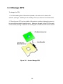
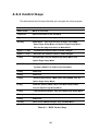
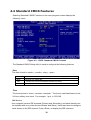
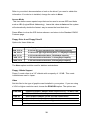
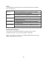
www.nexcom.com The Digital Infrastructure Single Board Computer PEAK 715-HT User's Manual PEAK715-HT Single Board Computer is compatible with multi-segmented backplanes and power supplies 2003-08 Edition Preface Copyright This document contains information protected by copyright. No part of this manual may be reproduced, copied, translated or transmitted in any form or by any means without the prior written consent from NEXCOM International Co., LTD. Disclaimer The information in this document is subject to change without prior notice and does not represent commitment from NEXCOM International Co., LTD. However, users may update their knowledge of any product in use by constantly checking its manual posted on our website: http://www.nexcom.com. NEXCOM shall not be liable for direct, indirect, special, incidental, or consequential damages arising out of the use of any product, nor for any infringements upon the rights of third parties which may result from such use. Any implied warranties of merchantability or fitness for any particular purpose is also disclaimed. Acknowledgements PEAK 715VL(2/2G/HT) is a trademark of NEXCOM International Co., LTD. All other product names mentioned herein are registered trademarks of their respective owners. Regulatory Compliance Statements This section provides the FCC compliance statement for Class A devices and describes how to keep the system CE compliant. FCC Compliance Statement for Class A Devices The product(s) described in this user’s guide has been tested and proved to comply with the limits for a Class A digital device, pursuant to Part 15 of FCC Rules. These limits are designed to provide reasonable protection against harmful interference when the equipment is operated in a commercial environment. This equipment generates, uses, and can radiate radio frequency energy and, if not installed and used in accordance with the user’s guide, may cause harmful interference to radio communications. Operation of this equipment in a residential area (domestic environment) is likely to cause harmful interference, in which case the user will be required to correct the interference (take adequate measures) at their own expense. CE Certification The product(s) described in this user’s guide complies with all applicable European Union (CE) directives if it has a CE marking. 1 Contents Chapter 1 General Information............................................. 5 1.1 Features..................................................................................6 1.2 Specifications.........................................................................6 1.3 PEAK 715HT Series Models ....................................................9 1.4 Checklist ................................................................................10 Chapter 2 Jumper Setting.....................................................11 2.1 Functions of Jumpers.............................................................12 2.2 Setting Jumpers.....................................................................13 2.3 Locating Jumpers...................................................................14 2.4 Setting CMOS CLEAR (JP2)....................................................15 2.5 Setting CPU Type (JP3).........................................................15 2.6 Setting Compact Flash Type (J15)........................................15 2.7 Setting Power Mode (J28, J17).............................................15 Chapter 3 Capability Expanding............................................16 3.1 System Memory......................................................................17 3.2 Installing DIMM......................................................................18 3.3 Change CPU............................................................................20 3.4 Installing the Fan Heatsink...................................................21 Chapter 4 Award BIOS Setup...............................................24 4.1 Entering Setup........................................................................25 4.2 The Main Menu .....................................................................26 4.3.1 Getting Help........................................................................28 4.3.2 Control Keys........................................................................29 4.4 Standard CMOS Features.......................................................30 4.5 Advanced BIOS Features........................................................34 4.6 Advanced Chipset Features....................................................38 4.7 Integrated Peripherals...........................................................41 4.8 Power Management Setup.....................................................44 4.9 PnP/PCI Configurations.........................................................47 4.10 PC Health Status..................................................................49 4.11 Frequency/Voltage Control..................................................50 4.12 Load Fail-Safe Defaults........................................................51 4.13 Load Optimized Defaults......................................................51 4.14 Set Supervisor/User Password............................................51 4.15 Save & Exit Setup................................................................52 4.16 Exit Without Saving.............................................................52 2 Chapter 5 Driver Installation ..............................................53 5.1 Find the Main Menu of Driver CD...........................................54 5.2 Installing VGA Driver.............................................................55 5.3 Installing INF.........................................................................58 5.4 Installing IAA.........................................................................60 Appendix A : Pin Assignments of Connectors.................................63 Appendix B : Watchdog Timer Setting............................................66 B.1 Watchdog Timer Working Procedure.....................................66 B.2 Watchdog Timer Control Register..........................................67 B.3 Watchdog Timer Programming Procedure.............................67 B.3.1 Power On or Reset the System...............................................67 B.3.2 Clear the WDT.........................................................................68 B.3.3 WDT Control Register.............................................................68 Tables Table 1-1 : Table 2-1 : Table 3-1 : Table 4-1 : Table B-1 : Table B-2 : Table B-3 : PEAK 715-HT Series Models..........................................9 Functions of Jumpers.................................................12 PEAK 715-HT Series DIMM Configurations..................18 BIOS Control Keys.....................................................29 Watchdog Timer Character and Function....................66 WDT Control Register Bit Definition............................67 WDT Control Register Initial Value.............................67 Figures Figure 1-1 : PEAK 715VL2G-HT Board Layout...............................10 Figure 2-1 : How to Set Jumpers..................................................13 Figure 2-2 : Jumper Locations......................................................14 Figure 3-1 : How to Install DIMM (1)...........................................18 Figure 3-2 : How to Install DIMM (2)...........................................18 Figure 3-3 : How to Install DIMM (3)...........................................19 Figure 3-4 : How to Install DIMM (4)...........................................19 Figure 3-5 : How to Change CPU ..................................................20 Figure 3-6 : Installing the Fan Heatsink (1)..................................22 Figure 3-7 : Installing the Fan Heatsink (2)..................................22 Figure 3-8 : Installing the Fan Heatsink (3)..................................22 Figure 3-9a : Installing the Fan Heatsink (4)................................23 Figure 3-9b : Installing the Fan Heatsink (5)................................23 Figure 3-9c : Installing the Fan Heatsink (6)................................23 Figure 3-10 : Installing the Fan Heatsink (7)................................23 3 Figure 4-1 : BIOS Main Menu........................................................26 Figure 4-2 : BIOS- Standard CMOS Features................................30 Figure 4-3 : BIOS- IDE Primary Master.........................................31 Figure 4-4 : BIOS- Advanced BIOS Features.................................34 Figure 4-5 : BIOS- Advanced Chipset Features.............................38 Figure 4-6 : BIOS- Integrated Peripherals...................................41 Figure 4-7 : BIOS- Power Management Setup..............................44 Figure 4-8 : BIOS- PnP/PCI Configurations..................................47 Figure 4-9 : BIOS- PC Health Status.............................................49 Figure 4-10 : BIOS- Frequency/ Voltage Control..........................50 4 Chapter 1 General Information 5 1.1 Features PEAK 715-HT Series is a memeber of NEXCOM’s P4-based SBC (single board computer) family. The features of this series are as follows: o o o o o o o o Socket 478 Intel® Pentium® 4 processor with 400/533MHz system bus up to 3.06 GHz or above, support Hyper-ThreadingTM technology Socket 478 Intel® Celeron® processor with 400 MHz system bus up to 2.0 GHz or above Intel® Pentium® 4-M processor with 400 MHz system bus up to 2.2 GHz or above Intel® 845GV Chipsets (B stepping) Max. 2GB DDR 333 SDRAM, DDR DIMM x 2 Intel® 82845GV chipset integrated Graphics controller with 64MB system memory Intel® 82551QM Ethernet controller x 1 for PEAK 715VL-HT; Dual Intel® 82551QM Ethernet controllers for PEAK 715 VL2-HT; Intel® 82551QM x 1 and Intel®82540EM Gigabit Ethernet controller x1 for PEAK 715VL2G-HT USB 2.0 port (480 Mbps) x 4 1.2 Specification System Architecture - Full size SBC with PCI/ISA gold-plated DIMMs - PCI V2.2 compliant - PICMG 1.0 (Rev.2.0) compliant CPU Support - Intel® Pentium® 4/Celeron® processor with 256K/512K L2 cache on-die; Intel® Pentium® 4-M processor with 512 KB L2 cache on-die - Support 400/533MHz system bus, CPU speed up to 3.06GHz or above - Support Hyper-ThreadingTM technology Main Memory - DDR DIMM x2 support maximum 2GB (DDR 200/266/333) of memory - Support single-sided/double-sided (Does not support double-sided x16 DDR DIMMs) - Support unbuffered non-ECC DIMMs only BIOS - Award System BIOS - Plug & Play support - Advanced power management support - ACPI 1.0b compliant - 4M bits flash ROM 6 Chipsets - Intel® 845GV (GMCH) chipsets (B stepping) - Intel® 82801DB x 1 I/O Controller Hub (ICH4) - Firmware Hub (FWH) 4M bits flash ROM x1 - PCI V2.2 compliant On Board LAN - Intel® 82551QM 10/100 Ethernet controller x1 for PEAK 715VL-HT - Dual Intel® 82551QM 10/100 Ethernet controllers for PEAK 715VL2-HT - Intel® 82551QM controller x1 and Intel® 82540EM Gigabit Ethernet controller x1 for PEAK 715VL2G-HT - Compliant with PCI V2.1/V2.2, IEEE802.3, IEEE 802.3u, IEEE802.3x, IEEE802.3y, IEEE802. 3ab - WfM 2.0 compliant - Drivers support: DOS/Windows®, Windows® 95/98/2000, Windows® NT, Netware 5.0, Linux - RJ45 with LED connector x 2 On Board VGA - Intel 82845GV (GMCH) chipset integrated with Graphics controller - Hardware motion compensation assist for software MPEG/DVD decode - 64MB VGA share Memory - Fully PC 98 and PC 99 Compliant - 15-pin CRT connector x1 On Chip I/O (ICH4) - On-board USB port (480 Mbps) x 4 (via NEXCOM’s proprietary USB cable) - Ultra ATA100/66/33 support, 40-pin connector x 2. On Board I/O - ITE 8712F-A Super I/O - SIO x 2, with 2 x 16C550 UARTs, 10-pin header x 2 - PIO x 1, bi-directional, EPP/ECP support, 26-pin connector x 1 - Floppy Disk controller: 34-pin connector x 1 - 6-pin mini DIN connector x1, for PS/2 keyboard/mouse, 5-pin connector x 1 (for external keyboard) - Optional on-board compact flash socket - On-board buzzer x1 - GPIO (4-in/4-out) 7 - On-board 2-pin header for I2C - On-board 2-pin header for reset SW / 2-pin for IDE active LED / 2 pin ATX power SW - One 3-pin power header for 3-pin power cable to connect to Backplane board and support ATX power-on function - On-board 4-pin additional power source input - AC97 output, 10-pin header x 1 - Optional Compact Flash Socket x 1 System Monitor - Derived from Super IO ITE 8712F-A to support system monitor - 8 voltage (For +1.5V, +3.3V, +5V, -5V, +12V, -12V, Vcore and Vcc5V Stand-By) - Monitoring CPU fan speed - Monitoring CPU & system temperatures ACPI Function ( Only when 3-pin power cable is connected to backplane and thus connected to ATX power source. ) - Soft power-off - Power-on by LAN - Power-on by Keyboard - Power-on by Ring Real Time Clock - On-chip RTC with one back-up external Li battery Watchdog Timer - Watchdog timeout programmable from 1, 2, 4, 8, …to 128 seconds PCI to ISA Bridge & ISAMAX Support - ITE 8888F x1 PCI to ISA Bridge - Provide 64mA driving capability to maximize expansion of ISA cards up to 20 ISA slots Dimensions - 338.58mm(L) x 122mm(W) Power Requirements Voltage Maximum +5V 12A +12V 8A 8 Environments - Operating temperature: 0°C to 60°C - Storage temperature: -20°C to 80°C - Relative humidity: 10% to 90% (Non-condensing) Certification - CE approval - FCC Class A 1.3 PEAK 715-HT Series Models The PEAK 715-HT single board computer series come in 3 models. The following table compares their main features: C hipsets Memory C hipsets Intergrated VGA Intel 82551QM 10/100 Ethernet Intel 82540EM Gigabit Ethernet PEAK 715VL2GHT Intel 845GV (B Steppi ng) D D R 333 Yes 1 port 1 port PEAK 715VL2-H T Intel 845GV (B Steppi ng) D D R 333 Yes 2 ports - PEAK 715VL-H T Intel 845GV (B Steppi ng) D D R 333 Yes 1 port - Table 1-1 : PEAK 715-HT Series Models 9 1.4 Checklist After opening the package of PEAK 715-HT Series, please check and make sure you have all of the following items: One PEAK 715-HT series SBC (An example of PEAK 715VL2G-HT is given below; please carefully examine every component of the board in case it lacks any.) One PEAK 715-HT Quick Reference Guide (the sticker printed with jumper info attached on the white box which packs the mainboard) One 50CM Cable JST 2.5mm 3 pin to 3 pin (5V standby ATX Power-on Cable) One Y Cable for Keyboard and Mouse One 180 mm AUX Power Cable (for J2) One Cable Set (FDD x1, SIO+PIO x1, SIO x1/Keyboard x1/IDE66 x1) One USB Cable with Bracket One Driver / Manual CD Figure 1-1 : PEAK 715VL2G-HT Board Layout 10 Chapter 2 Jumper Setting 11 2.1 Functions of Jumpers You can use jumpers to set configuration options. The table below defines function of each jumper: Connector Function JP 1 AC'97 JP 2 CMOS CLEAR JP 3 CPU Type Switch J1 FAN Connector J2 AUX +12V Power Connector J4 IDE Active LED J5 FAN Connector J6 GAL JTEC Connector J7 S p e a ke r J8 ATX Push button J9 SMBUS Connector J11 Hardware Reset J12 COM2 J13 COM1 J14 USB Connector J15 Compact Flash Type J16 ATX Power Connector J17 Power Mode J18 GPI/O Port (Super IO) J19 Keylock J20 IR Connector J21 Floppy Connector J22 PIO Port J23 External Keyboard Connector J24 Keyboard/Mouse Connector J25 LAN1 Connector J26 LAN2 Connector J27 (Optional) Cmpact Flash Socket J28 Power Mode J29 USB Connector IDE1 Secondary IDE Connector IDE2 Primary IDE Connector VGA1 VGA Connector Table 2-1: Functions of Jumpers 12 2.2 Setting Jumpers A jumper is the simplest kind of electric switch. It consists of two metal pins and a cap. When setting the jumpers, ensure that the jumper caps are placed on the correct pins. When the jumper cap is placed on both pins, the jumper is SHORT. If you remove the jumper cap, or place the jumper cap on just one pin, the jumpr is OPEN. Please see the following illustrations: The illustrations on the right show a 2-pin jumper. When the jumper cap is placed on both pins, the jumper is SHORT. If you remove the jumper cap, or place the jumper cap on just one pin, the jumper is OPEN. Open (Off) Short (On) These illustrations show a 3-pin jumper. Pins 1 and 2 are SHORT. Figure 2-1 : How to Set Jumpers 13 2.3 Locating Jumpers The illustration below shows the location of the mainboard jumpers: * = Pin 1 Figure 2-2 : Jumper Locations 14 2.4 Setting CMOS CLEAR (JP2) PIN NO. Description *1-2 Normal 2-3 Clear * Default Note: Clear CMOS procedure: 1. Turn off the power. 2. Short pin 2 and pin 3 of Jumper JP2. Wait 1~2 seconds. 3. Put the jumper cap back to pin 1 and pin 2. 4. After turning on the power, clear procedure is completed. 2.5 Setting CPU Type (JP3) PIN No. Description *N.C. P4/Celeron 1-2 P4-M * Default Note: Please turn off the power and change CPU before setting this jumper. 2.6 Setting Compact Flash Type (J15) PIN No. Description *1-2 Slave 2-3 Master * Default 2.7 Setting Power Mode (J28, J17) PIN No. Description *1-2 AT Power (Short) 2-3 ATX Power (Open) * Default 15 Chapter 3 Capability Expanding 16 3.1 System Memory Your system memory is provided by DIMM’s (Dual In-line Memory Modules) on the CPU board. The CPU board contains two memory banks: Bank 0 and 1, corresponds to connector DIMM1, DIMM2. The table below shows possible DIMM configurations for the memory banks. Please be noted that the PEAK 715-HT Series support Double Data (DDR333) SDRAM. Configurations using different brands of memory modules are not recommended. DIMM 1 DIMM2 Total Memory 128MB Empty 128MB Empty 128MB 128MB 128MB 128MB 256MB 256MB Empty 256MB Empty 256MB 256MB 256MB 256MB 512MB 512MB Empty 512MB Empty 512MB 512MB 512MB 512MB 1024MB 1024MB Empty 1024MB Empty 1024MB 1024MB 1024MB 1024MB 2048MB Table 3-1 : PEAK 715-HT Series DIMM Configurations 17 3.2 Installing DIMM To install DIMM: 1. Make sure the two handles of the DIMM sockets are in the “open” position, i.e. the handles stay outward. Figure 3-1 : How to Install DIMM (1) 2. Slowly slide the DIMM modules along the plastic guides in the both ends of the socket. Figure 3-2 : How to Install DIMM (2) 18 3. Then press the DIMM module down right into the socket, until a click is heard. That means the two handles automatically locked the memory modules into the right position of the DIMM socket. Figure 3-3 : How to Install DIMM (3) 4. To take away the memory module, just push the both handles outward, the memory module will be ejected by the mechanism in the socket. Figure 3-4 : How to Install DIMM (4) 19 3.3 Change CPU To change the CPU: 1. Pull the handling bar of the socket upward to the other end to loosen the socket’s openings. Carefully lift the existing CPU up to remove it from the socket. 2. Place the new CPU on the middle of the socket, orienting its beveled corner to line up with the socket’s beveled corner. Make sure the pins of the CPU fit evenly to the socket openings. Replace the handling bar to fasten the CPU to the socket. Figure 3-5 : How to Change CPU 20 3.4 Installing the Fan Heatsink Use the following instructions for installing the fan heatsink: 1. The heatsink has thermal interface material attached to the bottom, shown in Figure 3-7. Be careful not to damage the thermal interface material. 2. Align the fan heatsink and clip assembly (A in Figure 3-6) with the retention mechanism (the fan heatsink is symmetrical) and place it on the processor (as shown in Figure 3-7). Allow the heatsink base to compress (without rotating or twisting) the thermal interface material over the surface of the processor's integrated heat spreader. 3. With the clip levers (C in Figure 3-6) in the upward position, push down on all four clip frame corners (D in Figure 3-6) to secure the clip frame latches (E in Figure 3-6) to the retention mechanism hooks (F in Figure 3-6), as shown in Figure 3-8. Note: Make sure the processor fan cable is free from any obstruction and is not trapped under clip frame (B in Figure 3-6). 4. Note: It is important to not allow the heatsink to rotate or twist on the processor's integrated heat spreader. Securing the fan heatsink while closing the clip levers will ensure the thermal interface material is not damaged and the processor will operate correctly. Follow these steps, for closing the clip levers and ensuring the thermal interface material is not damaged: a. ) Make sure to close the clips levers in opposing directions, one at a time (levers require force to be completely closed), as shown in Figure 3-9a. First, close the clip lever (1 in Figure 3-9b), while holding the topside of the fan heatsink with your other hand (A in Figure 3-9b). b. ) Then, close the clip lever (2 in Figure 3-9c), while holding the topside of the fan heatsink with your other hand (B in Figure 3-9c). 5. Once the clip levers are closed, verify that the heatsink is securely retained and that the clip frame latches are properly engaged with the retention mechanism hooks. Note: When installed, the fan heatsink and clip assembly may cause the motherboard to slightly bend or flex. This provides the proper mechanical support for the processor (with attached fan heatsink and clip assembly) and helps prevent against damage during system shipment. 21 6. Lastly, connect the processor fan cable to the motherboard fan power header (Figure 3-10). Consult the motherboard manual to determine the correct fan header to use. Figure 3-6: Installing the Fan Heatsink (1) Fan Heatsink and Clip Assembly Terminology Figure 3-8: Installing the Fan Heatsink (3) Push Down Clip Frame Corners to Secure to Retention Mechanism Hooks Figure 3-7: Installing the Fan Heatsink (2) Align Fan Heatsink and Clip Assembly 22 Figure 3-9a: Installing the Fan Heatsink (4) Close Clip Levers, One at a Time Figure 3-9b: Installing the Fan Heatsink (5) Close Clip Lever (1), While Holding the Topside of Fan Heatsink (A) Figure 3-9c: Installing the Fan Heatsink (6) Close Clip Lever (2), While Holding the Topside of Fan Heatsink (B) Figure 3-10: Installing the Fan Heatsink (7) Connect Fan Cable to Motherboard 23 Chapter 4 Award BIOS Setup 24 Award’s BIOS ROM has a built-in Setup program that allows users to modify the basic system configuration. This type of information is stored in battery-backed RAM (CMOS RAM) so that it retains the Setup information when the power is turned off. 4.1 Entering setup Power on the computer and press <Del> immediately will allow you to enter Setup.The other way to enter Setup is to power on the computer. When the below message appears briefly at the bottom of the screen during the POST(Power On Self Test), press <Del> key or simultaneously press <Ctrl>, <Alt>, and <Esc> keys. TO ENTER SETUP BEFORE BOOT PRESS <CTRL-ALT-ESC> OR <DEL> KEY If the message disappears before you respond and you still wish to enter Setup, restart the system to try again by turning it Off then On or pressing the “RESET” button on the system case. You may also restart by simultaneously pressing <Ctrl>, <Alt>, and <Delete> keys. If you do not press the keys at the correct time and the system does not boot, an error message will be displayed and you will again be asked to: PRESS <F1> TO CONTINUE, <CTRL-ALT-ESC> OR <DEL> TO ENTER SETUP 25 4.2 The Main Menu Once you enter Award BIOS CMOS Setup Utility, the Main Menu (Figure 1) will appear on the screen. The main menu allows you to select from ten setup functions and two exit choices. Use arrow keys to select among the items and press <Enter> to accept or enter the sub-menu. Figure 4-1 : BIOS Main Menu Standard CMOS Features Use this menu for basic system configuration. Advanced BIOS Features Use this menu to set the Advanced Features available on the system. Advanced Chipset Features Use this menu to change the values in the chipset registers and optimize the system’s performance. Integrated Peripherals Use this menu to specify your settings for integrated peripherals. 26 Power Management Setup Use this menu to specify your settings for power management. PnP/PCI Configurations This entry appears if your system supports Plug and Play and PCI Configuration. PC Health Status Displays CPU, System Temperature, Fan Speed, and System Volt-ages Value. Frequency/Voltage Control Use this menu to specify CPU and memory frequency, and voltage control settings. Load Fail-Safe Defaults Use this menu to load the BIOS default values for the minimal/stable performance for your system to operate. Load Optimized Defaults Use this menu to load the BIOS default values, i.e., factory settings for optimal performance system operations. While Award has de-signed the custom BIOS to maximize performance, the factory has the option to change these defaults to meet their needs. Set Supervisor/User Password Enables you to change, set, or disable the supervisor or user pass-word. Save & Exit Setup Saves CMOS value changes to CMOS and exits setup. Exit Without Saving Ignores all CMOS value changes and exits setup. 27 4.3.1 Getting Help Main Menu The on-line description of the highlighted setup function is displayed at the bottom of the screen. Status Page Setup Menu/ Option Page Setup Menu Press F1 to pop up a small help window that describes the appropriate keys to use and the possible selections for the highlighted item. To exit the Help Window press <F1> or <Esc>. 28 4.3.2 Control Keys The table below lists the keys that help you navigate the setup program. Up arrow Move to previous item Down arrow Move to next item Left arrow Move to the item in the left hand Right arrow Move to the item in the right hand Esc key Main Menu -- Quit and not save changes into CMOS Status Page Setup Menu and Option Page Setup Menu -Exit current page and return to Main Menu PgUp / “+” key Increase the numeric value or make changes PgDn / “-“ key Decrease the numeric value or make changes F1 key General help, only for Status Page Setup Menu and Option Page Setup Menu (Shift) F2 key Change color from total 16 colors. F2 to select color forward, (Shift) F2 to select color backward F3 key Reserved F4 key Reserved F5 key Restore the previous CMOS value from CMOS, only for Option Page Setup Menu F6 key Load the default CMOS value from BIOS default table, only for Option Page Setup Menu F7 key Load the Setup default , only for Option Page Setup Menu F8 key Reserved F9 key Reserved F10 key Save all the CMOS changes, only for Main Menu Table 4-1 : BIOS Control Keys 29 4.4 Standard CMOS Features Selecting Standard CMOS Features on the main program screen displays the following menu: Figure 4-2 : BIOS- Standard CMOS Features The Standard CMOS Setup utility is used to configure the following features: Date The date format is <week>, <month>, <day>, <year>. Day Month Date Year The week, from Sun to Sat, determined by the BIOS and is display only The month, Jan. through Dec. The day, from 1 to 31 (or the maximum allowed in the month) The year, depend on the year of BIOS Time The times format in <hour> <minute> <second>. The time is calculated base on the 24-hour military-time clock. For example, 1 p.m. is 13:00:00. IDE Devices Your computer has two IDE channels (Primary and Secondary) and each channel can be installed with one or two devices (Master and Slave). Use these items to configure each device on the IDE channel. Press <Enter> to display the IDE submenu: 30 Figure 4-3 : BIOS- IDE Primary Master IDD HDD Auto-Detection If you want the Setup Utility to automatically detect and configure a hard disk drive on the IDE channel, press <Enter> while this item is highlighted. If your system has an IDE hard drive, you can use this utility to detect its parameters and enter them into the Standard CMOS Setup automatically. If the auto-detected parameters displayed do not match the ones that should be used for your hard drive, do not accept them. Press the <N> key to reject the values and enter the correct ones manually in the Standard CMOS Setup screen. (Note: If you are setting up a new hard disk drive that supports LBA mode, more than one line will appear in the parameter box. Choose the line that lists LBA for an LBA drive.) Do not choose Large or Normal if the hard disk drive is already fully formatted when you installed it. Select the mode that was used to format it. IDE Primary/Secondary Master/Slave If you leave this item at Auto, the system will automatically detect and configure any IDE devices it finds. If it fails to find a hard disk, change the value to Manual and then manually configure the drive by entering the characteristics of the drive in the items below: Capacity approximate hard disk drive capacity Cylinder number of cylinders Head number of heads Precomp write precompensation cylinder Landing Zone Sector landing zone number of sectors 31 Refer to your drive’s documentation or look on the drive if you need to obtain this information. If no device is installed, change the value to None. Access Mode This item defines some special ways that can be used to access IDE hard disks such as LBA (Logical Block Addressing). Leave this value at Auto and the system will automatically decide the fastest way to access the hard disk drive. Press <Esc> to close the IDE device submenu and return to the Standard CMOS Features page. Floppy Drive A and Floppy Drive B Options for these fields are: None No floppy drive installed 360K, 5.25 in 5-1/4 inch PC-type standard drive; 360 kilobyte capacity 1.2M, 5.25 in 5-1/4 inch AT-type high-density drive; 1.2 megabyte capacity 720K, 3.5 in 3-1/2 inch double-sided drive; 720 kilobyte capacity 1.44M, 3.5 in 3-1/2 inch double-sided drive; 1.44 megabyte capacity 2.88M, 3.5 in 3-1/2 inch double-sided drive; 2.88 megabyte capacity The None option could be used for diskless workstations. Floppy 3 Mode Support Floppy 3 mode refers to a 3.5" diskette with a capacity of 1.2 MB. This mode is sometimes used in Japan. Video Set this field to the type of graphics card installed in your system. If you are using a VGA or higher resolution card, choose the EGA/VGA option. The options are: EGA/VGA CGA 40 CGA 80 Mono Enhanced Graphics Adapter/Video Graphics Array. For EGA, VGA, SEGA, or PGA monitor adapters. Color Graphics Adapter, power up in 40 column mode Color Graphics Adapter, power up in 40 column mode Monochrome adapter, includes high resolution monochrome adapters 32 Halt On This setting determines which type of errors will cause the system to halt during boot. The options are: All Errors Whenever the BIOS detects a non-fatal error, the system will be stopped and you will be prompted. No Errors The system boot will not be stopped for any error that may be detected. All, But Keyboard The system boot will not stop for a keyboard error; it will stop for all other errors. All, But Diskette The system boot will not stop for a disk error; it will stop for all other errors. All, But Disk/Key The system boot will not stop for a keyboard or disk error; it will stop for all other errors. Base/Extended/Total Memory These items are automatically detected by the system at start up. These are display-only fields. You cannot make changes to these fields. After you have made your selections in the Standard CMOS Setup screen, press <ESC> to go back to the main screen. 33 4.5 Advanced BIOS Features Selecting Advanced BIOS Features on the main program screen displays this menu, which allows you to define advanced information about your system. You can make modifications to most of these items without causing fatal errors to your system. Figure 4-4 : BIOS- Advanced BIOS Features The following explains the options for each feature: Virus Warning Allows you to choose the Virus Warning feature for IDE Hard Disk boot sector protection. If this function is enabled and someone attempts to write data into this area, BIOS will show a warning message on screen and an alarm will beep. · Enabled: Activates automatically when the system boots up causing the following warning message to appear when anything attempts to access the boot sector or hard disk partition table: ! WARNING! Disk boot sector is to be modified Type “Y” to accept write or “N” to abort write Award Software, Inc. · Disabled: No warning message will appear when an attempt is made to access the boot sector or hard disk partition table. 34 CPU L1 & L2 Cache The choices are: Enabled, Disabled. Pentium 4 M CPU Speed This item allows user to choose the CPU speed to Low or High. The default is High. Hyper Threading Technology The Intel Hyper-Threading Technology allows a single processor to execute two or more separate threads concurrently. When hyper-threading is enabled, multithreaded software applications can execute their threads in parallel, thereby improving the processor’s performance. Quick Power On Self Test This item speeds up the Power On Self Test (POST) when you turn on the computer. If it is set to Enabled, BIOS will shorten or skip some check items during the POST. First/Second/Third Boot Device BIOS attempts to load the operating system from the devices in the sequence selected in these items. The available choices are Floppy, LS120, HDD-0, SCSI, CDROM, HDD-1, HDD-2, HDD-3, ZIP100, USB-FDD, USB-ZIP, USB-CDROM, USB-HDD, LAN, Disabled. Boot Other Device If the selected boot devices fail to boot, selecting Enabled for this item allows the BIOS to boot from other boot devices (in a predefined sequence) which are present but not selected as boot devices in the setup. Swap Floppy drive If the system has two floppy drives, use this item to swap the logical drive name assignments. Boot Up Floppy Seek Enable this to allow the system to search for floppy drives during the POST. Disable this item to boot faster. Boot Up NumLock Status Selects the power on state for NumLock. The available choices are Off and On. 35 Gate A20 Option Enables you to select whether the chipset or the keyboard controller should control Gate A20. The options are: · Normal: A pin in the keyboard controller controls Gate A20. · Fast: Lets chipset control Gate A20. Typematic Rate Setting If set to Enabled, enables you to set the Typematic Rate and Typematic Delay. Typematic Rate (Chars/Sec) This setting controls the speed at which the system registers held-down keystrokes. The choices range from 6 to 30 Chars/Sec. Typematic Delay (Msec) This setting controls the time between the display of the first character and successive characters. There are four delay choices: 250ms, 500ms, 750ms and 1000ms. Security Option Enables you to select whether the password is required every time the system boots or only when you enter Setup. System: The system will not boot and access to Setup will be denied if the correct password is not entered at the prompt. Setup: The system will boot, but access to Setup will be denied if the correct password is not entered at setup. APIC Mode The APIC Mode BIOS feature is used to enable or disable the motherboard’s APIC (Advanced Programmable Interrupt Controller). If your single-processor motherboard supports APIC and you are using a Win32 operating system (Windows NT, 2000 and XP), it’s recommended that you enable this feature to allow faster and better IRQ handling. If you are using a multiprocessor motherboard, you must enable this feature because it’s required for IRQ handling in multiprocessor systems. 36 MPS Version Control for OS This feature is only applicable to multiprocessor motherboards as it specifies the version of the Multi-Processor Specification (MPS) that the motherboard will use. The MPS is a specification by which PC manufacturers design and build Intel architecture systems with two or more processors. MPS version 1.4 is required for a motherboard to support a bridgeless secondary PCI bus. OS Select for DRAM > 64MB Set to OS2 if the system memory size is greater than 64 MB and the operating system is OS/2. HDD S.M.A.R.T Capability Built in problem-detection capability (Self-Monitoring Analysis and Reporting Technology) of hard disk drives signals warning of any foreseen problem. The choices are: Enabled, Disabled. 37 4.6 Advanced Chipset Features Figure 4-5 : BIOS- Advanced Chipset Features DRAM Timing Selectable The Choices are: Manual, By SPD. Set the latter to enable the system to automatically set the SDRAM timing by SPD (Serial Presence Detect). SPD is an EEPROM chip on the DIMM module that stores information about the memory chips it contains, including size, speed, voltage, row and column addresses, and manufacturer. CAS Latency Time When synchronous DRAM is installed, the number of clock cycles of CAS latency depends on the DRAM timing. Do not reset this field from the default value specified by the system designer. Active to Precharge Delay The choices: 5,6,7 DRAM RAS# to CAS# Delay The choices: 2, 3. DRAM RAS# Percharge The choices are 2 and 3. 38 Turbo Mode This item allows you to enable or disable the memory turbo mode. The choices : Enabled and Disabled. Memory Frequency For The choices are DDR266, DDR333, and Auto. System BIOS Cacheable Selecting Enabled allows caching of the system BIOS ROM at F0000h-FFFFFh, resulting in better system performance. However, if any program writes to this memory area, a system error may result. The available choices are Enabled, Disabled. Video BIOS Cacheable Selecting Enabled allows caching of the video BIOS ROM at C0000h, resulting in better video performance. However, if any program writes to this memory area, a system error may result. The choices : Enabled, Disabled. Memory Hole At 15M-16M In order to improve performance, certain space in memory is reserved for ISA cards. This memory must be mapped into the memory. The choices : Enabled, Disabled. Delayed Transaction The chipset has an embedded 32-bit posted write buffer to support delay transactions cycles. Select Enabled to support compliance with PCI specification version 2.1. Delay Prior to Thermal The choices: 4,8,16,32 Mins. AGP Aperture Size(MB) Select the size of Accelerated Graphics Port (AGP) aperture. The aperture is a portion of the PCI memory address range dedicated for graphics memory address space. Host cycles that hit the aperture range are forwarded to the AGP without any translation. The choices are from 4 in doubles up to 256. 39 On-Chip VGA Setting includes: On-chip VGA The choices are Enabled, Disabled. On-chip Frame Buffer Size The choices are 1MB, 8 MB. Boot Display The choices are Auto, CRT, TV, EFP. 40 4.7 Integrated Peripherals Figure 4-6 : BIOS- Integrated Peripherals Onboard LAN Boot ROM Decides whether to invoke the boot ROM of the onboard LAN chip. The available choices are LAN1, LAN2, and Disabled. On-Chip Primary/Secondary PCI IDE The system chipset contains a PCI IDE interface with support for two IDE channels. Select Enabled to activate the primary and/or secondary IDE interface. Select Disabled to deactivate this interface, if you install a primary and/or secondary add-in IDE interface. IDE Primary/Secondary Master/Slave PIO The four IDE PIO (Programmable Input/Output) fields let you set a PIO mode (0-1) for each of the four IDE devices that the onboard IDE interface supports. Modes 0 through 4 provide successively increased performance. In Auto mode, the system automatically determines the best mode for each device. The choices are: Auto, Mode 0, Mode 1, Mode 2, Mode 3, Mode 4. IDE Primary/Secondary Master/Slave UDMA Ultra DMA/33 implementation is possible only if your IDE hard drive supports it and the operating environment includes a DMA driver (Windows 95 OSR2 or a thirdparty IDE bus master driver). If your hard drive and your system software both support Ultra DMA/33, select Auto to enable BIOS support. The choices are: Auto, Disabled. 41 USB Controller Select Enabled if your system contains a Universal Serial Bus controller and you have USB peripherals. USB 2.0 Connector Select Enable if your system contains a Universal Serial Bus 2.0 controller and you have USB peripherals. USB Keyboard Support Select Enabled if your USB controller is enabled and it needs USB keyboard support in legacy (old) OS operating systems such as DOS. AC97 Audio Selecting Auto will enable the AC97 audio if it is detected onboard. AC97 Modem Selecting Auto will enable the AC97 modem, if it is detected onboard. Init Display First This item allows you to active PCI slot or onboard display first. The choices are: PCI slot, Onboard/AGP. IDE HDD Block Mode Block Mode transfers can improve the access to IDE devices. Enable this item if your IDE devices support block mode transfers. Power ON Function Select the different manners for powering on the system. The choices: Keyboard 98, Password, Any KEY, Hot KEY, BUTTON ONLY, Mouse Click, Mouse Move. KB Power ON Password The system will ask for a password. After entering the correct password, the keyboard starts running. Hot Key Power ON The choices are: Ctrl+F1,Ctrl+F2,......Ctrl+F12. 42 Onboard FDC Controller Select Enabled if your system has a floppy disk controller (FDC) installed on the system board and you wish to use it. If you install an add-in FDC or the system has no floppy drive, select Disabled in this field. Onboard Serial Ports (1, 2) Select an address and corresponding interrupt for the first and second serial ports. The choices: Auto, 3F8/IRQ4, 3E8/IRQ4, 2F8/IRQ3, 2E8/IRQ3, Disabled. UART Mode Select This item allows you to select UART mode. The choices: Normal, IrDA, ASKIR, SCR. UR2 Duplex Mode The choices: Half, Full. Onboard Parallel Port This item allows you to determine access On-Board parallel port controller with which I/O address. The choices: 378/IRQ7, 278/IRQ5, 3BC/IRQ7, Disabled. Parallel Port Mode Select an operating mode for the On-Board parallel (printer) port. Select Normal, Compatible, or SPP unless you are certain your hardware and software both support one of the other available modes. The choices: SPP, ECP, EPP, ECP + EPP. ECP Mode Use DMA Select a DMA channel for the port. The choices: 1, 3. 43 4.8 Power Management Setup Figure 4-7 : BIOS- Power Management Setup Power Supply Type The choices: AT, ATX. Soft-Off by PWRBTN (Power Button) Pressing the power button for more than 4 seconds forces the system to enter the Soft-Off state when the system “hangs”. The available choices are Delay 4 Seconds, Instant-Off PWRON After PWR-Fail This setting specifies whether your system reboots after a power failure. There are three selections: Off: The system will remain off when power comes back after a power failure. On: The system will switch on when power comes back after a power failure. Former-Sts: The system will return to the last state before the power failure when power returns. ACPI Function This item allows you to Enable/Disable the Advanced Configuration and Power Interface (ACPI). The Choice: Enabled, Disabled. 44 Power Management This category allows you to select the type (or degree) of power saving and is directly related to the following modes: 1. HDD Power Down 2. Suspend Mode There are three selections for Power Management; three of them have fixed mode settings. Min. Power Saving: Minimum power management. Suspend Mode = 1 hr., and HDD Power Down = 15 min. Max. Power Saving: Suspend Mode = 1 min., and HDD Power Down = 1 min. User Define: Allows you to set each mode individually. When not disabled, each of the ranges are from 1 min. to 1 hr. except for HDD Power Down which ranges from 1 min. to 15 min. and Disabled. Video Off Method This determines the manner in which the monitor is blanked. There are three choices: 1. V/H SYNC+Blank: This selection will cause the system to turn off the vertical and horizontalsynchronization ports and write blanks to the video buffer. 2. Blank Screen: This option only writes blanks to the video buffer. 3. DPMS: Initial display power management signaling. Video Off In Suspend This determines the manner in which the monitor is blanked. The Choices: Yes, No. Suspend Type Select the Suspend Type. The Choices: PwrON Suspend, Stop Grant. MODEM Use IRQ This determines the IRQ in which the MODEM can use. The Choice: 3, 4, 5, 7, 9, 10, 11, NA. Suspend Mode When enabled and after the set time of system inactivity, all devices except the CPU will be shut off. The choices are: 1~2 min, 2~3 min,... up to 1 hour. 45 HDD Power Down When enabled and after the set time of system inactivity, the hard disk drive will be powered down while all other devices remain active. Wake-Up by Ring/LAN The choices: Enabled, Disabled. Resume by Alarm When Enabled, your can set the date and time at which the RTC (real-time clock) alarm awakens the system from Suspend mode. The choice: Enabled, Disabled. Reload Global Timer Events Primary IDE 0 Primary IDE 1 Secondary IDE 0 Secondary IDE 1 FDD, COM, LPT Port PCI PIRQ[A-D] # The events are I/O events whose occurrence can prevent the system from entering a power saving mode or can awaken the system from such a mode. In effect, the system remains alert for anything which occurs to a device which is configured as Enabled, even when the system is in a power down mode. The choices: Enabled, Disabled. 46 4.9 PnP/PCI Configurations Figure 4-8 : BIOS- PnP/PCI Configurations PNP OS Installed Select Yes if the system operating environment is Plug-and-Play aware (e.g. Windows 95). The Choices: Yes, No. Reset Configuration Data Normally, you leave this field Disabled. Select Enabled to reset Extended System Configuration Data (ESCD) when you exit Setup if you have installed a new add-on Card and the system reconfiguration has caused such a serious conflict that the operating system can not boot. The choices: Enabled, Disabled . Resources Controlled By The Award Plug and Play BIOS has the capacity to automatically configure all of the boot and Plug and Play compatible devices. However, this capability means absolutely nothing unless you are using a Plug and Play operating system such as Windows95. If you set this field to Manual, then choose specific resources by going into each of the submenus that follows this field. The Choice: Auto (ESCD), Manual. 47 PCI/VGA Palette Snoop Leave this field at Disabled. The Choices: Enabled, Disabled. Assign IRQ for VGA Assign an IRQ for VGA. The Choices: Enabled, Disabled. Assign IRQ for USB Assign an IRQ for USB. The Choices: Enabled, Disabled. PCI Latency Timer (CLK) This item controls how long each PCI device can hold the bus before another takes over. INT Pin 1~4 Assignment Name the interrupt request (IRQ) line assigned to PCI 1 through PCI 4 on your system. Activity of the selected PCI slot awakens the system. The choices: Auto, 3, 4, 5, 7, 9, 10, 11 Onboard LAN 1, 2 INT Assign The choices: Auto, 3, 4, 5, 7, 9, 10, 11 48 4.10 PC Health Status Figure 4-9 : BIOS- PC Health Status System Monitor Device Default is Enabled. Select Disabled can release IO range 294h to 297h for other device. The choices: Enabled, Disabled. Shutdown Temperature This item allows you to set up the CPU shutdown temperature. This item is only effective under Windows 98 ACPI mode. The Choices: Disabled, 60 0C/140 0F, 65 0C/149 0F, 70 0C/158 0F. 49 4.11 Frequency/Voltage Control Figure 4-10 : BIOS- Frequency/Voltage Control CPU Clock Ratio This item allows you to set up the CPU clock ratio, but this function depends on different CPU performance. It is only effective for those clock ratio that have not been locked. Auto Detect PCI Clk When enabled, this item will auto detect if the PCI sockets have devices and will send clock signal to PCI devices. When disabled, it will send the clock signal to all PCI sockets. The choices: Enabled, Disabled. Spread Spectrum Modulated This item allows you to enable/disable the spread spectrum modulate to reduce EMI. The choices: Enabled, Disabled. 50 4.12 Load Fail-Safe Defaults This option opens a dialog box that lets you install fail-safe defaults for all appropriate items in the whole setup utility. Use this option if you have changed your system and it does not operate correctly or does not power up. 4.13 Load Optimized Defaults This option opens a dialog box that lets you install optimized defaults for all appropriate items in the whole Setup Utility. Press the <Y> key and then <Enter> to install the defaults. Press the <N> key and then <Enter> to not install the defaults. The optimized defaults place demands on the system that may be greater than the performance level of the components, such as the CPU and the memory. You can cause fatal errors or instability if you install the optimized defaults when your hardware does not support them. If you only want to install setup defaults for a specific option, select and display that option, and then press the <F7> key. 4.14 Set Supervisor/User Password The Supervisor/User Password utility sets the password. The mainboard is shipped with the password disabled. If you want to change the password, you must first enter the current password, then at the prompt enter your new password. The password is case sensitive. You can use up to eight alphanumeric characters. Press <Enter> after entering the password. At the next prompt, confirm the new password by retyping it and pressing <Enter> again. To disable the password, press <Enter> instead of entering a new password when the Enter Password dialog box appears. A message appears confirming that the password has been disabled. If you have set supervisor and user passwords, only the supervisor password allows you to enter the BIOS Setup Program. Note: If you forget your password, the only way to solve this problem is to discharge the CMOS memory by turning power off and placing a shunt (jumper cap) on jumper JP2 to short pin 2 and pin 3 for five seconds, then putting the shunt back to pin 1 and pin 2 of JP2. 51 4.15 Save & Exit Setup Selecting this option and pressing <Enter> will save the new setting information in the CMOS memory and continue with the booting process. 4.16 Exit Without Saving Selecting this option and pressing <Enter> will exit the Setup Utility without recording any new values or changing old ones. 52 Chapter 5 Driver Installation 53 PEAK 715-HT Series come with a driver installation CD-ROM that enables you to install VGA driver software, INF(Intel Chipset Software Installation Utility) and IAA (Intel Application Accelerator). 5.1 Find the Main Menu of Driver CD Please follow the following steps to find VGA driver, INF and IAA in the driver CDROM to implement installation. Note: In this manual, Windows 2000 is the model for OS operation system. Step 5.1.1 Place the driver installation CD-ROM in your CD-ROM driver. Then cick My Computer on your desktop items. Step 5.1.2 The menu of My Computer will display. Find your drive which supports CD-ROM and click that item. Step 5.1.3 Select DRIVER folder. 54 Step 5.1.4 The menu of the driver installation CD will display. You can see the folders of VGA, INF and IAA installation driver. 5.2 Installing VGA Driver Step 5.2.1 Double click the folder of VGA. The menu will display. Select the folder of WIN2K_XP for Windows 2000 operating system. Step 5.2.2 After the menu displays, select the folder of GRAPHICS. 55 Step 5.2.3 After this screen displays, double click the blue sign SETUP. Step 5.2.4 After a sequence of system processing, you will see a static screen instructing the installation process. Click Next to continue setup. Step 5.2.5 If you accept License Agreement, click Yes to continue. 56 Step 5.2.6 Select Yes to continue. Step 5.2.7 Click Yes. Step 5.2.8 An installation wizard will inform successful completion of driver software installation and ask you to restart your computer. Select “Yes, I want to restart my computer now,” and then click Finish. After your computer reboots, VGA driver is already setup in your computer. 57 5.3 Installing INF After installing VGA driver, go back to 5.1. Go through step 5.11 to step 5.14 again, and open the folder of INF to start installing INF. Step 5.3.1 Open the folder of 98_ME_2K_XP. Step 5.3.2 Double click the blue sign INFINST_AUT OL. Step 5.3.3 Click Next to install INF. 58 Step 5.3.4 Click Yes to continue. Step 5.3.5 Click Yes. Step 5.3.6 Select Yes, I want to restart my computer now. Then click Finish. INF is installed. 59 5.4 Installing IAA After installing INF, go back to 5.1. Go through step 5.11 to step 5.14 again, and open the folder of IAA to start installing INF. Step 5.4.1 After the folder of ALL_OS displays, click it.. Step 5.4.2 Double click the blue sign IATA_CD. Step 5.4.3 Click Next to install. 60 Step 5.4.4 Click Yes. Step 5.4.5 Click Next. Step 5.4.6 Select Next. 61 Step 5.4.7 Click Yes. Step 5.4.8 Select Yes, I want to restart my computer now, then click Finish. Your computer is installed with IAA. 62 Appendix A : Pin Assignments of Connectors JP1 : AC97’ PIN No. Description PIN No. Description 1 AC_SDOUT 2 VCC3 3 AC_RST# 4 GND 5 AC_SYNC 6 +12V 7 AC_SDIN0 8 AC_SDIN1 9 AC_BTCLK 10 AC_SDIN2 J14 : USB Connector PIN No. J19 : Keylock Description PIN No. Description 1 VCC5 1 VCC5 2 USBP0N 2 N.C 3 USBP0P 3 GND 4 USBP1N 4 Keylock 5 USBP1P 5 GND 6 GND J18 : GPIO PORT (Super IO) PIN No. Description PIN No. Description 1 GP20 (PIN27) 2 GP24 (PIN23) 3 GP21 (PIN26) 4 GP25 (PIN22) 5 GP22 (PIN25) 6 GP26 (PIN21) 7 GP23 (PIN24) 8 GP27 (PIN20) 9 GND 10 GND 63 J 20 : IR Connector PIN No. J 23 : External Keyboard Connector Description PIN No. Description 1 VCC5 1 Keyclk 2 CIRRX 2 Keydata 3 IRRX 3 N.C 4 GND 4 GND 5 IRTX 5 VCC5 J 9 : SMBUS Connector J 8 : ATX Push Button PIN No. PIN No. Description Description 1 SMBDATA 1 GND 2 SMBCLK 2 Plus Signal J 11 : Hardware Reset PIN No. J 16 : ATX Power Connector Description PIN No. Description 1 GND 1 5VSBY 2 Reset # 2 GND 3 64 PSON # J 7 : Speaker PIN No. J 4 : IDE Active LED Description PIN No. Description 1 Speaker Out 1 VCC5 2 GND 2 IDE_ACT# 3 GND 4 VCC5 J 2 : AUX +12 V Power Connector PIN No. Description 1 GND 2 GND 3 +12V 4 +12V 65 Appendix B : Watchdog Timer Setting B.1 Watchdog Timer Working Procedure Watchdog Timer (WDT) is a special hardware device that monitors the computer system during normal operation. WDT has a clock circuit that times down from a set number to zero. If a monitored item occurs before the timer reaches zero, WDT resets and counts down again. If for some reason the monitored item doesn’t occur before the timer reaches zero, WDT performs an action, such as a diagnostic operation (rebooting the computer). You must enter timer values into WDT Configuration Register (Write the control value to the Configuration Port), and clear WDT counter (read the Configuration Port). WDT Configuration port Watch Dog Timer WDT Active Time F2 Default at F2 Disabled 1. Default at disabled Enabled 2. Enabled for user’s programming 1 sec Default at 64 sec 2 sec 4 sec 8 sec 16 sec 32 sec 64 sec 128 sec Table B-1 : Watchdog Timer Character and Function 66 B.2 Watchdog Timer Control Register The Watchdog Timer Control Register controls the WDT working mode. Write the value to the WDT Configuration Port. The following table describes the Control Register bit definition: Table B-2 : WDT Control Register Bit Definition B.3 Watchdog Timer Programming Procedure · B.3.1 Power On or Reset the System The initial value of WDT Control Register (D3~D0) is zero (0), when power is on or the system has been reset. The following table indicates the initial value of WDT ( 00000000b ) : Bit Value Mean 3 0 Disable Watchdog Timer 2, 1, 0 000 Select 64 second Table B-3 : WDT Control Register Initial Value 67 B.3.2 Clear the WDT WDT counter interval cannot be longer than the preset time, otherwise, WDT sends a reset signal to the system. The following is an example of clearing the WDT program in Intel 8086 assembly language. ; ( Clear the WDT) Mov dx, F2h ;Setting the WDT configuration port In al, dx Note: Before running WDT, you must clear WDT to ensure that the initial value is zero. B.3.3 WDT Control Register Note: This register writes to WDT configuration port. Set WDT Control Register to control the WDT working mode. The initial value of WDT Control Register is shown as follows: ; (Setting the WDT Control Register as AL) Mov al, 0h ; Setting initial value = 0 for the WDT Control Register Follow these instructions to set the register: 1. Select the time-out intervals of WDT (decide the values of D2, D1, D0 in F2 ) Example: If D2~D0 = 0, the time-out interval is 64 seconds. AND 2. al, 11111000b ; Setting the time-out interval as 64 sec. Enable or Disable WDT ( decide D3 value in F2) i.e. D3=0, Disables WDT AND al, 11110111b ; Disable the WDT 68 i.e. D3=1, Enables WDT OR al, 00001000b ; Enable the WDT After finishing the above settings, you must output the Control Register’s value to WDT Configuration Port. Then WDT will start according to the above settings. MOV OUT dx, F2h dx, al ; Setting WDT Configuration Port ; Output the Control Register Value 69 The Digital Infrastructure C Copyright 2003 NEXCOM International Co., Ltd. Version 1.0