1
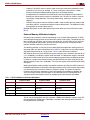
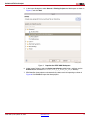
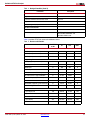
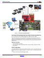
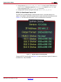
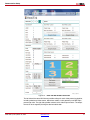
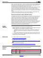
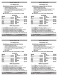
Application Note: Kintex-7 Family
Real Time Video Engine 2.0 Implementation in
Kintex-7 FPGAs
XAPP1091 (v1.0.1) March 18, 2014
Summary
Author: Bob Feng and Kavoos Hedayati
In the broadcast video landscape, video content with various formats flows across acquisition,
contribution, distribution, and consumption sectors. To properly archive, distribute, and display
the content, the video signal often needs to be properly processed with the appropriate format
conversion. For example, to correctly display NTSC/PAL signals on a FHD LCD screen, a
series of deinterlacing, scaling, chroma upsampling, and color correction operations must be
performed, as well as alpha blending.
This application note leverages the latest Xilinx® Kintex™-7 FPGA architecture to provide a
truly scalable video processor reference design to serve multi-stream/multi-pipeline video
processing needs. It is targeted for applications like multi-viewer display, video switches, and
multichannel video routers, as well as multi-stream up-down converters.
Introduction
This broadcast-quality video processing reference design is targeted to a wide range of video
applications. The Real Time Video Engine Reference Design version 2.0 (RTVE 2.0) primarily
performs video de-interlacing and scaling, and includes other features such as a triple-rate SDI
interface, DVI interface, on-screen display (OSD), video frame buffer control, chroma
resampler, and color space conversion. The video processing function in this design is
scalable, support for 2x, 4x, and up to 8x parallel video pipelines.
RTVE 2.0 includes the following features:
•
On-the-fly switchable video sources: HDMI and Triple Rate SDI
•
Support for progressive or interlaced format video
•
Multiple video output ports: HD/3G-SDI and HDMI
•
Scalable design optimized for different FPGAs:
•
•
•
2-pipeline - XC7K160T logic density
•
4-pipeline - XC7K160T logic density
•
Up to 8-pipeline - XC7K325T logic density
Completely based on Xilinx AXI infrastructure:
•
AXI-Lite CPU control interface
•
AXI-Memory Map for external memory access
•
AXI-Streaming for video streaming among video processing blocks
Full-featured video processing on every pipeline:
•
Motion-Adaptive and Edge-Adaptive deinterlacer
•
Polyphase scaler with and on-the-fly customizable coefficient table
•
10-bit 4:4:4 processing engine
•
Frame buffer readback
•
On-the-fly window resizing and magnifying glass function
•
Composite onto video output with graphic overlay
© Copyright 2013–2014 Xilinx, Inc. Xilinx, the Xilinx logo, Artix, ISE, Kintex, Spartan, Virtex, Vivado, Zynq, and other designated brands included herein are trademarks of Xilinx
in the United States and other countries. All other trademarks are the property of their respective owners.
XAPP1091 (v1.0.1) March 18, 2014
www.xilinx.com
1
RTVE 2.0 FPGA Design
•
RTVE 2.0 FPGA
Design
•
Live video picture-in-picture
•
Professional fade-in/fade-out effect
•
Contrast enhancement through Color Correction Matrix
Web server-based control GUI
The core video processing engine in the RTVE 2.0 design is built on OmniTek's state-of-the-art
OSVP Scalable Video Processor [Ref 1] (see Figure 1). The OSVP contains a series of
configurable video pipelines supporting x2, x4, and x8 parallel processing. Each pipeline
consists of chroma upsampling, color space conversion, deinterlacing, cropping,
scaling/resizing, and video output frame synchronization. In addition, each OSVP is equipped
with one or two built-in multiport video DMA blocks (depending on the number of processing
pipelines) to streamline, balance, and arbitrate all external memory access requests from all
video processing blocks.
The OSVP fully adopts Xilinx AXI4 peripheral bus technology. Its control plane is directed from
an AXI4-Lite interface, external memory access is through one or two AXI4-MM interfaces, and
video input and output are carried from AXI4-Streaming interfaces. This makes it highly
compatible with the Xilinx design environment and methodology.
X-Ref Target - Figure 1
AXI4-Lite CPU Interface
CPU Backplane
RGB or YUV
4:2:2 or 4:4:4
AXI-4 Stream
Video
RGB or YUV
4:2:2 or 4:4:4
AXI-4 Stream
Video
RQ
Chroma
Upsampler
Color Space
Converter
Deinterfacer
Cropper
Deinterfacer
Frame Store
Frame
Store
Resizer
Frame Sync
Multiport DMA
OSVP v1.0
AXI4-MM Memory Interface
X1091_01_040113
Figure 1:
OmniTek Scalable Video Processor
Leveraging the AXI4 infrastructure, the OSVP is easily integrated with other Xilinx IP building
blocks including video streaming input and output, Microblaze™ soft processor,
On-Screen-Display (OSD) LogiCORE™, Video Time Controller (VTC) LogiCore, and
AXI-Interconnect and AXI-DDR to form a full-featured Real Time Video Engine. Figure 2
illustrates the design architecture.
XAPP1091 (v1.0.1) March 18, 2014
www.xilinx.com
2
RTVE 2.0 FPGA Design
X-Ref Target - Figure 2
SDRAM
MIG DDR3
AXI4-MM
AXI Interconnect
AXI4-MM
HDMI Rx
XSVI
AXI4Stream
Crosspoint
SDI
1- 8 Rx
XSVI
Chroma
Upsample
Colour
Matrix
Deinterlacer
Crop
Resizer
Frame
Sync
OSD
Combiner:
1-8 Video
+
Graphics
x N Channels
Video
1-8
OSD
Output
XSVI
AXI4Stream
Video 1 - 8
Chroma
Subsample
VTC
Crosspoint
AXI4Stream
Overlay
SDI Tx
CCM
HDMI Tx
AXI-Lite
MicroBlaze
Input Video Module
OmniTek
Component
Video Processing
Module
Xilinx IP Core
AXI4-MM
Video Output
Module
Non-Productized
Component
AXI4-Lite
AXI4-Stream
System Module
Interrupt
Controller
GigE Phy
RGMII I/F
XSVI
X1091_02_031213
Figure 2:
RTVE 2.0 Design Block Diagram
Video Input
The RTVE 2.0 supports up to eight SDI and one HDMI input sources. The supported input
formats are:
•
SDI: SD-NTSC, SD-PAL, HD-1080i, HD-1080p, HD-720p
•
HDMI: 480p, 576p, 720p, 1080i, 1080p
Video Output
The RTVE v2.0 generates video output on all interfaces (HDMI and SDI) concurrently. The
output format is user selectable among the 720p50, 720p60, 1080p50, and 1080p60 rates. The
output frame rate is derived from the input frame rate and matched with either frame repeat or
frame drop. For example, deinterlacing and scaling a 480i 59.94 Hz input to a 720p60 or
1080p60 output results in frame repeat. Similarly, if the output format is set at 720p50 or
1080p50, proper frame drop occurs.
Video Processing
The key video processing function blocks are:
•
Chroma Upsampling: The OSVP conducts a straight 4:4:4 10-bit processing pipeline for
the best possible picture quality. Incoming 4:2:2 video streams are pre-upsampled to 4:4:4
streams.
•
Color Space Conversion: The OSVP allows conversion between a wide range of color
spaces.
•
Deinterlacing: The OSVP uses motion- and edge-enhancement techniques to convert an
interlaced input video to an equivalent progressive video format. Additionally, the OSVP
can detect film-mode-based cadences such as 2:2 and 3:2 pull down. The OSVP then
corrects the video to reconstruct the original video format.
XAPP1091 (v1.0.1) March 18, 2014
www.xilinx.com
3
RTVE 2.0 FPGA Design
•
Cropping: The OSVP allows a specific region of the input video to be selected for further
processing. This occurs, for example, in a 4:3 or 16:9 aspect ratio switch on a video
stream that transports different footage types (films and advertisements).
•
Scaling/Resizing: In the OSVP, the scaler/resizer takes the progressive output from the
deinterlacer and resizes the image to a new output size. The user can select a variety of
input/output scaling operations: up-scaling, down-scaling, zooming, and aspect ratio
adjusting.
•
OSD: By taking outputs from the OSVP, the OSD is used to render the final scaled image
with video, graphics, and text overlay onto the output video streams. The OSD block allows
overlapping of up to eight video streams.
Detailed descriptions of each video processing function block are in the OSVP User Guide
[Ref 1].
External Memory Utilization Analysis
Efficient memory utilization is key to implementing a truly scalable video processor. In OSVP,
each video processing pipeline has five concurrent memory access ports. The deinterlacer has
two read and one write ports, the resizer has one write port, and the OSD has one read port.
For an eight-pipeline configuration, up to 40 concurrent access ports are required. Actual
memory utilization varies on a case-by-case basis.
The following provides a case analysis for multiple pipeline configurations working with 4:4:4
interlaced video, with 30-bit color delivered at a rate of 75 x 106 pixels/s and all video windows
displayed without overlap on a single screen. Table 1 shows the memory utilization.
With video of this format, each deinterlacer read or write port sees a maximum data flow of 40
x 75 = 3,000 Mb/s, including the motion vector overhead. The deinterlacer output is streamed
directly to the OSVP resizer input. Because the video being processed by the different pipelines
is shown on a single screen without overlap, the total flow from the resizer write ports of the
different pipelines is 30 x 150 = 4,500 Mb/s. This value also applies to the total flow to the OSD
read ports.
While summing these factors provides the absolute maximum data flow, the OSVP reduces its
bandwidth requirement by restricting the data processed to just the active image and spreading
its processing of any line over the whole of a single line sweep. This allows the required
maximum data flow to be reduced by a factor corresponding to the difference between the
actual line length and the active line length. In this example case, that corresponds to an
average maximum data flow that results by multiplying the calculated total by 0.93091.
Table 1: RTVE 2.0 Memory Utilization Breakdown
2-pipeline OSVP
4-pipeline OSVP
8-pipeline OSVP
Deinterlacer
(3,000 x 3) x 2 = 18,000 Mb/s
(3,000 x 3) x 4 = 36,000 Mb/s
(3,000 x 3) x 8 = 72,000 Mb/s
Resizer
4500 Mb/s
4500 Mb/s
4500 Mb/s
OSD
4500 Mb/s
4500 Mb/s
4500 Mb/s
Total
27000 Mb/s
45000 Mb/s
81000 Mb/s
Average
25134.6 Mb/s
41891 Mb/s
75403.6 Mb/s
The x2 and x4 configurations are well suited with a DDR3 64-bit 800 Mb/s memory setup. For
the x8 configuration, DDR3 64-bit 1,600 Mb/s is needed to fully leverage the Xilinx Kintex-7
FPGA performance advantage.
XAPP1091 (v1.0.1) March 18, 2014
www.xilinx.com
4
Build the RTVE 2.0 Project
Build the RTVE
2.0 Project
The following example walks through detailed steps to build a x4 OSVP-configured RTVE 2.0
design.
Project Directory Structure
The RTVE 2.0 project directory structure is shown in Figure 3.
X-Ref Target - Figure 3
Pre-compiled
Bitstream and
Microblaze
Software
EDK Hardware
Project Files
SDK Software
Workspace
X1091_03_031313
Figure 3:
RTVE 2.0 Project Directory Structure
Tools
The project is implemented based on a complete Xilinx EDK flow, so ISE Design Suite 14.4
Embedded Edition or later must be used. The hardware must first be built using EDK. The SDK
project can then be built to deploy the FPGA BIT file and MicroBlaze processor software onto
the KC705 development system.
EDK Hardware Build
These steps are used to build the EDK hardware:
1. Launch XPS (Xilinx Platform Studio).
2. Select and load the rtve_2_0_kc705_4x.xmp project file from the
release\rtve_2_0_kc705_4x_hw directory as shown in Figure 3. The EDK screen
should resemble a system view, with all the connectivity of the various pcores used by the
RTVE 2.0 design shown in Figure 4.
XAPP1091 (v1.0.1) March 18, 2014
www.xilinx.com
5
Build the RTVE 2.0 Project
X-Ref Target - Figure 4
X1091_04_031213
Figure 4: RTVE 2.0 XPS Build
3. On the Menu bar, select Device Configuration, then select Update Bitstream.
This step first builds a FPGA bitstream rtve_2_0_kc705_4x.bit under
release\rtve_2_0_kc705_4x_hw\implementation\ directory and updates the
bitstream with MicroBlaze processor bootstrap binary code.
The updated bitstream is saved into a new file named download.bit.
SDK Software Build
The RTVE 2.0 software resides in a local SDK Workspace, with all RTVE 2.0-specific drivers
contained within the hierarchy of the RTVE 2.0 project. All built-in Xilinx drivers are
automatically located by SDK.
Use the following steps to create the SDK software.
1. To create a new user workspace in the hierarchy of the RTVE 2.0 at a fixed directory level,
select File > Switch Workspace > Other.
EDK exports files to the default location relative to the top directory in the project.
2. In the dialog box, ensure that the directory ends with the SDK directory in
release\rtve_2_0_kc705_4x_sw\sw\SDK_Workspace (see Figure 5).
XAPP1091 (v1.0.1) March 18, 2014
www.xilinx.com
6
Build the RTVE 2.0 Project
X-Ref Target - Figure 5
X1091_05_031213
Figure 5:
Set up the RTVE 2.0 SDK Workspace
3. To ensure that the automatic build process can locate all drivers immediately after the
import process is complete, add the local driver repository specific to the RTVE 2.0 project
before importing the project.
a. Select Xilinx Tools > Repositories.
b.
In the top field labeled Local Repositories - (available to the current workspace), click
New and browse to the …\repository directory and select it.
c.
Click OK to accept the new local repository of drivers.
Figure 6 shows the window after the repository has been added.
X-Ref Target - Figure 6
X1091_06_031213
Figure 6:
Set Up RTVE 2.0 SDK Repositories
4. To import the predefined software and hardware projects from which SDK builds the RTVE
reference software, select File > Import.
XAPP1091 (v1.0.1) March 18, 2014
www.xilinx.com
7
Build the RTVE 2.0 Project
5. In the Import dialog box, select General > Existing Projects into Workspace as shown in
Figure 7, and click Next.
X-Ref Target - Figure 7
X1091_07_031213
Figure 7:
Populate the RTVE SDK Workspace
6. Under Import Projects, select the Select root directory radio button, and then use the
Browse button to locate the release\rtve_2_0_kc705_4x_sw\sw directory.
7. SDK identifies three projects and automatically selects each for importing as shown in
Figure 8. Click Finish to import the three projects.
XAPP1091 (v1.0.1) March 18, 2014
www.xilinx.com
8
Build the RTVE 2.0 Project
X-Ref Target - Figure 8
X1091_08_031213
Figure 8:
Import All Three RTVE 2.0 Software Projects
At this point, SDK locates all drivers and builds the software.
8. In a successful build, the Microblaze software rtve_kc705.elf is generated in the
release\rtve_2_0_kc705_4x_sw\sw\SDK_Workspace\Debug directory.
Table 2 provides a checklist for the reference design.
Table 2: Design Checklist
Parameter
Desription
Simulation
Functional simulation performed
Y
Timing simulation performed
N
Testbench used for functional and timing
simulations
Functional Only
Testbench format
VHDL
Simulator software/ version used
Modelsim 6.6d
XAPP1091 (v1.0.1) March 18, 2014
www.xilinx.com
9
Build the RTVE 2.0 Project
Table 2: Design Checklist (Cont’d)
Parameter
Desription
SPICE/IBIS simulations
NA
Implementation
Synthesis software tools/version used
ISE 14.4
Implementation software tools /versions used
ISE 14.4
Static timing analysis performed
Y
Hardware Verification
Hardware verified
Y
Hardware platform used for verification
KINTEX-7 KC705 plus TED
TB-TB-FMCH-3GSDI2A and
TB-FMCL-HDMI cards
Table 3 provides RTVE 2.0 resource breakdown values.
Table 3: Resource Utilization
BRAM/FIFO
36 bit
FF
LUT
DSP
OSVP2 (2 input channels)
108
22240
18412
102
OSVP4 (4 input channels)
192
41398
34623
204
OSVP8 (8 input channels)
379
80500
69406
408
SDI Input (per input channel)
0
1,900
2,500
0
SDI Output
0
409
445
0
HDMI Input
0
405
287
0
HDMI Output
0
79
53
0
AXI Interconnect: CPU Peripherals
0
2,000
1,091
0
AXI Interconnect: High Bandwidth
0
12,231
8,056
Onscreen Display (4 channels)
2
5,093
2,983
12
MicroBlaze
19
3,168
7,850
6
DDR3 MIG (supporting 4–8 channels)
0
17,891
15,511
0
Video Timing Controller
0
764
757
0
2-input RTVE 2.0
149
83,695
73,937
183
4-input RTVE
243
105,801
96,547
291
Kintex 7 160T resources
325
202,800
101,400
600
8-input RTVE
415
158,013
136,767
504
Kintex 7 325T resources
445
407,600
203,800
840
OSVP Core
Supporting IP
Totals
XAPP1091 (v1.0.1) March 18, 2014
www.xilinx.com
10
Demonstration Setup
Demonstration
Setup
The following 4x configuration demonstration consists of two parts: hardware setup and
software setup. To load the software into the FPGA, the following are required and included in
the project file:
•
A pre-generated FPGA bit stream kc705_4x.bit
•
A pre-compiled Microblaze firmware binary kc705_rtve_4x.elf
•
An image file image.mfs
•
An FPGA configuration script start_kc_4x.tcl
Hardware Inventory
The following hardware is required for the demonstration:
•
One Xilinx KC705 Evaluation Board: XC7K325T-2FFG900 FPGA
•
One TED TB-FMCH-3GSDI2A card
•
One TED HDMI 1.3 Rev 3 (TB-FMCL-HDMI)FMC card (providing HDMI input and output)
•
One HDMI monitor supporting at least 720p@60 Hz(1280x720 p@60)
•
Four SD/HD/3G SDI Video Sources
•
One HDMI video source(optional)
•
One HDMI cable
•
Four mini-din SDI cables
•
One WiFi Ethernet router (providing DHCP server)
•
One Ethernet cable
•
One Micro USB cable (for FPGA configuration)
•
One Mini USB cable (optional for UART debugging)
•
One PC with at least two free USB ports
Hardware Setup
The hardware setup is illustrated in Figure 9. The TED TB-FMCH-3GSDI2A card must be
plugged in to High Pin Count (HPC) FMC connector on the KC705 evaluation board. The TED
TB-FMCL-HDMI card must be plugged into LPC FMC connector on the KC705 evaluation
board.
XAPP1091 (v1.0.1) March 18, 2014
www.xilinx.com
11
Demonstration Setup
X-Ref Target - Figure 9
HDMI Video Source
Control PC
HDMI Monitor
SDI Video Input
Coming From
SDI Video Source
Wireless
Router
Xilinx KC705 Board +
TED HDMI FMC +
TED SDI 2A
Figure 9:
SDI Video
Signal Analyzer
X1091_09_031213
KC705 RTVE 2.0 Demo Setup
Figure 10 shows the demo setup with wire connections. The CH0-RX, CH1-RX, CH2, and CH3
connectors on the TED TB-FMCH-3GSDI2A card are connected to four SDI video sources
using the mini-din SDI cables. Optionally, a HDMI source can be fed into the TB-FMCL-HDMI
RX port.
XAPP1091 (v1.0.1) March 18, 2014
www.xilinx.com
12
Demonstration Setup
X-Ref Target - Figure 10
SDI
SDI
HDMI
SDI
HDMI
SDI
SDI
FPGA JTAG
Configuration
RJ45
X1091_10_031213
Figure 10:
RTVE 2.0 Design Block Diagram
The video output can be monitored through either a HDMI or SDI monitor. The HDMI output is
driven through the TB-FMCL-HDMI TX port. The SDI outputs are driven through CH0-TX and
CH1-TX connectors on the TB-FMCH-3GSDI2A card. Both use mini-din cables.
The KC705 Ethernet port must be connected to the wireless router LAN port so that an IP
address can be allocated to the RTVE 2.0. If a bundled Kintex-7 FPGA broadcast video kit is
desired, TB-7K-325T-BVK-RTVE can be purchased from Xilinx ecosystem partner Inrevium’s
website [Ref 3].
Software Inventory
•
Microsoft Windows 7/XP/Vista
•
Xilinx ISE 14.4 or newer version design tools package (including all necessary KC705
device drivers)
FPGA Configuration
To configure the Kintex-7 FPGA on the KC705 Board FPGA, connect a micro USB cable to the
KC705 micro USB port through the control PC as shown in Figure 10, and then perform these
steps:
1. Launch Xilinx Microprocessor Debugger (XMD).
XAPP1091 (v1.0.1) March 18, 2014
www.xilinx.com
13
Demonstration Setup
2. Change directory to release\ready_for_download, where prebuilt FPGA bitstream
download.bit, Microblaze software kc705_rtve.elf, image file image.mfs, and
FPGA configuration script start_kc_4x.tcl are located.
3. Configure the FPGA by running the command source start_kc_4x.tcl.
RTVE 2.0 Web-Based Control GUI
The RTVE 2.0 is controlled through a web-based GUI, which is accessed through an IP
address. This address is found in the output screen's system status box at the top-right corner
(Figure 11). The status box also provides all input and output format information.
X-Ref Target - Figure 11
X1091_11_031213
Figure 11:
System Status Text Overlay Box
To open the RTVE 2.0 control GUI (see Figure 12), open a web browser, type the IP address in
the address bar, and press Enter.
XAPP1091 (v1.0.1) March 18, 2014
www.xilinx.com
14
Demonstration Setup
X-Ref Target - Figure 12
X1091_12_031213
Figure 12:
RTVE 2.0 Web-based Control GUI
The left side of the control GUI shows possible settings for each video processing pipeline,
including selection of video source, deinterlacer modes, scaler geometry, and OSD alpha
percentage value. The right side provides controls to the video output screens. The output
format can be changed by clicking the desired radio button.
XAPP1091 (v1.0.1) March 18, 2014
www.xilinx.com
15
Design Advisory
Initially, a quadratic layout diagram is shown on the bottom right side. Clicking the Next Layout
button rotates the various preset layouts. The size of any of the four video windows can be
changed by clicking and dragging the window's border or corner.
Click and hold within a window to move it anywhere in the output screen. Windows can overlap
each other. Changing the alpha blending percentage value for each window enables
picture-in-picture capability. RTVE 2.0 allows a maximum of eight windows to overlap each
other with individually controllable transparency, which can be used to deliver fade-in/fade-out
effects.
In addition, the GUI software allows each processed video pipeline's Resizer output to be
captured by clicking the Snapshot Scaler button on the top right side.
Recommended Demonstrations and Benchmarks
To effectively use the two major RTVE building blocks (the deinterlacer and the scaler), Xilinx
recommends using professional video benchmark tools containing enough diagonal lines,
motions, chroma color bursting, film mode cadences, and other challenging sequences.
Due to the limitations inherent in transmitting NTSC/PAL interlaced video through the
HDMI/DVI interface, Xilinx recommends using the SDI interface to benchmark both
deinterlacing and scaling functions. The video content can be transmitted from a professional
video server through its native SDI interface, or by running from a regular DVD player to a
HDMI/DVI-to-SDI conversion box. For example, see the video interface converter at
http://www.blackmagic-design.com/products/dviextender/.
Design
Advisory
This section provides design advisories for the RTVE demonstration.
•
HDMI RX Video Mode: The NTSC/PAL video reception through the HDMI RX port on the
TB-FMCL-HDMI card is not supported. The limitation is twofold:
•
References
•
The HDMI specification does not mandate support for NTSC/PAL. Therefore, the
transmission capability of this video format is dependent on the individual media
player.
•
The TB-FMCL-HDMI Hardware User Manual [Ref 2] does not support NTSC or PAL.
2:2 Film Mode Cadence Detection: Depending on the media content and player, the 2:2
cadence might not always be detectable.
1. OmniTek Scalable Video Processor (OSVP) User Guide
http://omnitek.tv/sites/default/files/OSVP.pdf
2. TB-FMCL-HDMI Hardware User Manual
http://solutions.inrevium.com/products/pdf/pdf_TB-FMCL-HDMI_HWUserManual_3.00e.p
df
3. Kintex-7 FPGA Broadcast Video Kit
http://solutions.inrevium.com/products/kits/broadcast/tb-7k-325t-bvk.html
Revision
History
The following table shows the revision history for this document.
Date
Version
04/05/2013
1.0
03/18/2014
1.0.1
XAPP1091 (v1.0.1) March 18, 2014
Description of Revisions
Initial Xilinx release.
Corrected figure reference to Figure 5.
www.xilinx.com
16
Notice of Disclaimer
Notice of
Disclaimer
The information disclosed to you hereunder (the “Materials”) is provided solely for the selection and use of
Xilinx products. To the maximum extent permitted by applicable law: (1) Materials are made available "AS
IS" and with all faults, Xilinx hereby DISCLAIMS ALL WARRANTIES AND CONDITIONS, EXPRESS,
IMPLIED, OR STATUTORY, INCLUDING BUT NOT LIMITED TO WARRANTIES OF
MERCHANTABILITY, NON-INFRINGEMENT, OR FITNESS FOR ANY PARTICULAR PURPOSE; and (2)
Xilinx shall not be liable (whether in contract or tort, including negligence, or under any other theory of
liability) for any loss or damage of any kind or nature related to, arising under, or in connection with, the
Materials (including your use of the Materials), including for any direct, indirect, special, incidental, or
consequential loss or damage (including loss of data, profits, goodwill, or any type of loss or damage
suffered as a result of any action brought by a third party) even if such damage or loss was reasonably
foreseeable or Xilinx had been advised of the possibility of the same. Xilinx assumes no obligation to
correct any errors contained in the Materials or to notify you of updates to the Materials or to product
specifications. You may not reproduce, modify, distribute, or publicly display the Materials without prior
written consent. Certain products are subject to the terms and conditions of the Limited Warranties which
can be viewed at http://www.xilinx.com/warranty.htm; IP cores may be subject to warranty and support
terms contained in a license issued to you by Xilinx. Xilinx products are not designed or intended to be
fail-safe or for use in any application requiring fail-safe performance; you assume sole risk and liability for
use of Xilinx products in Critical Applications: http://www.xilinx.com/warranty.htm#critapps.
XAPP1091 (v1.0.1) March 18, 2014
www.xilinx.com
17