1
STMicroelectronics Spirit1 Radio Module
Overview, power consumption and integration
Analog and TLC Electronics
Prof: Dante Del Corso
Student: Emilio Fazzoletto
Emilio Fazzoletto - Analog and TLC Electronics - 2015
Pag. 1
Summary
Chapter 1: ST Microelectronics Spirit1 Module ........................................................................... 4
1.1
Introduction – block diagram ............................................................................................................ 4
1.2 Operating Specifications .......................................................................................................................... 7
1.2.1 Functional Modes ................................................................................................................................. 7
1.2.2 Transmission and Reception............................................................................................................. 7
1.2.3 Data Modes ...................................................................................................................................... 9
1.3 Power Output Configuration and Supported Modulations ..................................................................... 9
1.3.1 Power Output Configuration ............................................................................................................ 9
1.3.2 Supported Modulations.................................................................................................................. 10
1.4 Overview on supported modulations .................................................................................................... 10
1.4.1 Binary frequency-shift keying (2-FSK)............................................................................................. 11
1.4.2 Minimum-shift keying (MSK) .......................................................................................................... 12
1.4.3 Gaussian frequency-shift keying (GFSK) ......................................................................................... 12
1.4.4 Amplitude-shift keying (ASK) ......................................................................................................... 13
1.4.5 On-off keying (OOK)........................................................................................................................ 13
1.5 Packets management engine ................................................................................................................ 14
1.6 Interfacing with a micro-controller ....................................................................................................... 14
1.7 Advanced functionality .......................................................................................................................... 16
1.7.1 Low Duty Cycle Reception Mode (LDCR) ............................................................................................ 16
1.7.2 CSMA/CA engine............................................................................................................................. 16
1.7.3 AGC ................................................................................................................................................. 16
1.7.4 Temperature Sensor ....................................................................................................................... 16
1.7.5 AES Engine ...................................................................................................................................... 16
1.7.7 Data encoding and integrity check ................................................................................................. 17
1.7.8 Link Layer Protocol ......................................................................................................................... 17
Chapter 2: iNemo M1 + Spirit1: Real Time Clock Synchronization .............................................. 18
2.1 Introduction ........................................................................................................................................... 18
2.2 Implementation ..................................................................................................................................... 18
Chapter 3: Power Consumption Characterization ..................................................................... 21
3.1 MCU in Standby Mode........................................................................................................................... 24
3.2 System battery life simulation ............................................................................................................... 25
Chapter 4: design of a PCB integrating the Spirit1 module ......................................................... 27
2
4.1 Idea ........................................................................................................................................................ 27
4.2 System Block Diagram ........................................................................................................................... 27
4.3 Schematic and PCB development .......................................................................................................... 28
References ............................................................................................................................... 33
3
Chapter 1: ST Microelectronics Spirit1 Module
1.1 Introduction – block diagram
The Spirit 1 is a low-power low-datarate RF transceiver capable to operate in sub-GHz bands. I have chosen
it as radio module due to its small package, low power consumption and high flexibility. It matches the
tipical WSN (wireless sensor network) system specifications.
The available frequency bands start from 150MHz and goes up to 956MHz: the supported digital
modulations are 6 (2-FSK, GFSK, MSK,GMSK, OOK, e ASK) and the datarate goes up to 500kbps. In
the following chapters there is an overview about the functional modes, protocols, I/O, and all
main features such as the encryption engine.
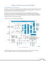
In Figure 1 you can see the Spirit1 block diagram.
Figure 1 – Spirit1 Block Diagram
In the block diagram is possible to see at least 5 important digital components: the LNA (Low Noise
Amplifier), two Mixers, two ADCs, a Power Amplifier and a Frequency Synthesizer.
4
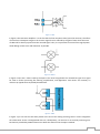
Figure 2 - LNA
In figure 2 the Low Noise Amplifier: it is the first block of the reception chain (apart the antenna). The effect
of noise from subsequent stages in the receiver signal chain is reduced by the gain of LNA, while the noise
of LNA itself is directly injected into the received signal. Thus, it is imperative for LNA to boost signal power
while adding as little noise and distortion as possible.
Figure 3 - Mixers
In figure 3 there are 2 mixers used by the Spirit1. The mixer brings down the received RF signal to IF signal
for ease in further processing like filtering, amplification, and digitization. Two mixers are necessary to
realize a QA (quadrature-amplitude) demodulator.
Figure 4 - ADCs
In figure 4 you can see the two ADCs placed at the end of the analog receiving chain in order to digitalize
the information stream. The digitalized data can, subsequently, can be sent to an external processing unit.
No data are provided by STMicroelectronics about the ADCs used in the Spirit1 module.
5
Figure 5 - Power Amplifier
In the transmitting chain a power amplifier (PA, in figure 5) converts a low-power radio-frequency signal
into a larger signal of significant power in order to drive the antenna (the Spirit1 uses only 1 antenna both
for transmission and reception). The input is generated by the RF synthesizer, while the output level can be
configured between -30 dBm and +11 dBm in 0.5 dB steps
Figure 6 - Frequency Synthesizer
A frequency synthesizers (figure 6) generate the feeding signal of the PA. The Spirit1 includes a fast startup
frequency synthesizer with a settling time of 6 μs and the typical frequency resolution is 33Hz. A crystal
connected to XIN and XOUT is used to provide a clock signal to the frequency synthesizer. The allowed clock
signal frequency is either 24, 26, 48, or 52 MHz. As an alternative, an external clock signal can be used to
feed XIN for proper operation.
6
1.2 Operating Specifications
1.2.1 Functional Modes
The Spirit1 is equipped with a controller which switches the functional mode between two main ones:
transmission (TX) and reception (RX). There are also other states and the complete FSM (finite state
machine) is shown in figure 7.
Figure 7 – Spirit1 state diagram
At the power on the device is in Ready State and starting from it the Spirit1 can reach the Standby,
Lock or Sleep mode. The Lock state is a mandatory transition state to pass through in order to
reach the TX/RX. Standby and Sleep, on the other hand, allow to reduce by a different amount the
power consumption. In particular the Sleep mode is suitable for short idle period whereas Standby
is much more indicated for long inactivity period: it allows the highest reduction in consumption
but needs a more complex and long re-configuration before starting the operation.
1.2.2 Transmission and Reception
The Spirit1 is a radio module capable of both transmission and reception: it allows a bidirectional
communication. The module can stay in TX and RX for different time periods depending on some dedicated
registers which, programmed by the user, determine the behavior of the device.
In the following lists are reviewed the available management modes for both TX and RX.
7
The device continues to stay in TX mode
Until the transmission of the current packet ends
Until the TX buffer (TXFIFO) is not empy if the selected mode is Direct Mode
Until e SABORT (Spirit Abort) instruction
State reached after the transmission
TX, if Persistent-TX is selected
Protocol, if the automatic retransmission is selected
Ready State, if no protocol is acitve and the TX ends successfully
The device continue to stay in RX mode
Until the reception of the current packet ends
Until the RX timeout is reached
While Direct Mode is active, until a SABORT instruction or until the RXFIFO is full
State reached after the reception
RX, if Persistent-RX is active
Protocol, if the auto-acknoledgement is active
Ready, if the RX end successfully and the Low Duty Cycle Mode Reception (LDCR) is not
active
Sleep, in case of LDCR
8
1.2.3 Data Modes
In Direct Mode is possible to bypass the data framing/deframing and also the data buffering
normally used on the I/O register of the Spirit1. In particular using two registers, TXSOURCE and
PCKTCTRL1, is possible to select one of the following data treatment options
0 – normal mode
1 – direct through FIFO: data packets have to be written, by the external MCU (the Micro
Controller Unit which is using the Spirit1), directly in the TX FIFO: no processing will be
automatically performed, the user is responsible for the data coding
2 – direct through GPIO o direct mode: the data are reading in “real time” using a GPIO
specially programmed for this function. Data are transmitted without any processing. The
transmission is synchronized using a clock which has to be transmitter on a second GPIO
3 – PN9 mode: an internal generator create a pseudo-random binary sequence: this mode
is suitable for test purpose only
The TX FIFO register, as well as the RX FIFO, has 96 byte. This two FIFO registers has 2
programmable thresholds usable to have information about the filling status of the registers.
1.3 Power Output Configuration and Supported Modulations
1.3.1 Power Output Configuration
The power output level can be modified using the 8 bit PA_LEVEL register. The user can save up to 8
different power levels in order to obtain ascending and descending power ramps in order to, for example,
model the symbols of an ASK (“Amplitude Shift Keying”) modulation. The maximum output power is
11 dBm (16 in TX boost mode, using additional external hardware in addition at the standard
configuration), the minimum is -34dBm.
The PA_RAMP_ENABLE register enables the power ramping. It is possible to configure both the
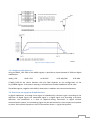
steps number and the steps width. In figure 8 a power ramping example is showed: there are two
different ramps in black and in blue.
9
Figure 8 – Power ramping example
1.3.2 Supported Modulations
Using the MOD_TYPE field of the MOD0 register is possible to choose between 5 different digital
modulations:
MOD_TYPE:
00 2-FSK
01 GFSK
10 ASK/OOK
11 MSK
If MOD_TYPE=10 the choice between ASK and OOK depends on the configuration of the
PA_POWER register: if the power ramping is activated then the ASK modulation will be used.
The MOD0 register, together with MOD1, determines in addition the transmission datarate.
1.4 Overview on supported modulations
In digital modulation, an analog carrier signal is modulated by a discrete signal. According to one
definition of digital signal, the modulated signal is a digital signal, and according to another
definition, the modulation is a form of digital-to-analog conversion. In digital wireless
communication systems, the modulating signal may be represented as a time sequence of symbols
or pulses. Each symbol represents n bits of information where n = log2m bits/symbol.
10
Advantages of Digital over Analog:
Greater noise immunity (due to its finite process)
Robustness to channel impairments
Easier multiplexing of various forms of information like voice, data, video
Security – by using coding techniques to avoid jamming
Accommodation of digital error control codes which detect and/or correct transmission
errors
Equalization to improve the performance of over all communication link
Supports complex signal conditioning and processing methods
1.4.1 Binary frequency-shift keying (2-FSK)
Frequency shift keying (FSK) is the most common form of digital modulation in the highfrequency radio spectrum, and has important applications in telephone circuits
BFSK uses a pair of discrete frequencies to transmit binary (0s and 1s) information
The demodulation of a binary FSK signal can be done using very efficient algorithms, even
on low-power microcontrollers
Figure 9 - Example of BFSK modulation
11
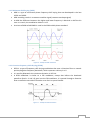
1.4.2 Minimum-shift keying (MSK)
MSK is a type of continuous-phase frequency-shift keying that was developed in the late
1950s and 1960s
MSK encoding results in a constant-modulus signal (constant envelope signal)
In MSK the difference between the higher and lower frequency is identical to half the bit
rate: as a result, the modulation index m is 0.5
A variant of MSK called GMSK is used in the GSM mobile phone standard.
Figure 10 - Example of MSK modulation
1.4.3 Gaussian frequency-shift keying (GFSK)
GFSK is a type of frequency shift keying modulation that uses a Gaussian filter to smooth
positive/negative frequency deviations, which represent a binary 1 or 0
It is used by Bluetooth: the minimum deviation is 115 kHz
A GFSK modulator is similar to a FSK modulator, except that before the baseband
waveform (levels −1 and +1) goes into the FSK modulator, it is passed through a Gaussian
filter to make the transitions smoother so to limit its spectral width
Figure 11 - Example of GFSK modulation
12
1.4.4 Amplitude-shift keying (ASK)
ASK is a form of amplitude modulation that represents digital data as variations in the
amplitude of a carrier wave
ASK uses a finite number of amplitudes, each assigned a unique pattern of binary digits.
Usually, each amplitude encodes an equal number of bits. Each pattern of bits forms the
symbol that is represented by the particular amplitude
Like AM, ASK is also linear and sensitive to atmospheric noise, distortions, propagation
conditions on different routes
Figure 12 - Example of ASK modulation
1.4.5 On-off keying (OOK)
OOK denotes the simplest form of (ASK) modulation that represents digital data as the
presence or absence of a carrier wave
OOK is more spectrally efficient than frequency-shift keying, but more sensitive to noise
On-off keying is most commonly used to transmit Morse code over radio frequencies
Figure 13 - Example of OOK modulation
13
1.5 Packets management engine
Before the transmission data can be interested in a framing operation. The Spirit1 allows a high
flexibility in order to customize the data packet structure. Using dedicated register is possible to
chose between three standard options: Stack (with auto-acknowledge), WMBus ( “Wireless MeterBus”) and Basic.
A really important feature is the Automatic Packet Filtering. There are 4 different filter criteria
supported:
CRC (Cyclic Redundancy Check) Filtering
Destination Address Filtering
Source Address Filtering
Control Field Filtering
1.6 Interfacing with a micro-controller
The Spirit1 module is equipped with two main interfaces: a standard 4-pin SPI port and 4
programmable GPIO pins.
The SPI interface can be used to send command to the Spirit1, to read/write configuration
registers and to read/write data in the TX/RX buffer FIFOs. The 4 GPIO pin I 4 pin can be used for
the interrupt management and to send unbuffered data to the transmitter.
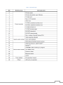
The interrupt status is available in the IRQ_STATUS[3:0] bits. In table 1 there are the supported
interrupts which can be generated by the Spirit1.
14
Table 1 – Spirit1 Interrupts
15
1.7 Advanced functionality
1.7.1 Low Duty Cycle Reception Mode (LDCR)
The Spirit1 can operate in a particular functional mode called Low Duty Cycle which allows to use
the device with very low power consumption without suspend the transceiver operations. In LDCR
the Spirit1 controller is configured to use the low-frequency internal RC oscillator (34,7kHz)
instead of the external crystal (used in this case for the RF Synthesize only). The non used
functional blocks are shut-down.
1.7.2 CSMA/CA engine
The device has an embedded CSMA (Carrier Sense Multiple Access) which is optionally usable. This
module is dedicated to manage the multiple access on the channel using the carrier sensing. This
protocol, level MAC of the ISO/OSI standard, avoid collisions between multiple devices operating
on the same physical channel.
1.7.3 AGC
The AGC algorithm (Automatic Gain Control) is used to keep the output power level inside the
limits specified by the user. Using an upper and a lower limits the AGC algorithms will vary the
output signal gain in order to track the output power target.
1.7.4 Temperature Sensor
A temperature sensor is embedded on the chip and its analog voltage signal can be available on
the GPIO0. When used the sensor increase the absorbed current of about 400uA in Standby,
Ready and Sleep states.
1.7.5 AES Engine
The integrated cryptographic coprocessor implements the 128-bitbit AES ('Advanced Encryption
Standard) standard. This peripheral can be used through 3 128-bit registers
AES_KEY_IN: register used to provide to the coprocessor the encryption key
AES_DATA_IN: register used to provide input data
AES_DATA_OUT: read only register, it provides the encrypted data
The AES engine works on 128 bit data-blocks with 128 bit encryption key and provides 4 different
operations:
Data encryption starting from a given key
Calculus of the decryption key starting from the encryption one
Data decryption starting from a given decryption key
Data decryption using a given encryption key
16
1.7.7 Data encoding and integrity check
The device has error detection and correction capabilities which can be activated by the user
depending on the security level requested by the application.
The CRC protocol is available with a 8, 16 or 24 bit checksum. Taking about the error correction
capabilities there is a FEC (Forward Error Correction) engine with a soft Viterbi coding with a ratio
equal to 0.5 and k=4.
1.7.8 Link Layer Protocol
About link layer protocols the user can configure the device in order to use the auto-ACK and autoretransmission functionalities if the selected packet framing is STack. To improve the transmission
efficiency is also possible to use the auto-ACK with Piggybacking.
17
Chapter 2: iNemo M1 + Spirit1: Real Time Clock Synchronization
2.1 Introduction
In a wireless sensor network is very important to acquire and transmit not only data but their time stamps
too. In order to obtain a set of data correctly correlated is necessary that the all the devices on the field are
synchronized and it is really important also to power-on the interested devices only when necessary
increasing their battery life.
Typical WSN devices are very often cheap and with limited calculus capabilities. The only power source is
almost everytime a small integrated battery and in order to maximize the autonomy devices have to use
low power modes when they are not active. In addition the time synchronization is also critical to assure
that when a device returns active there will be at least another node ready to communicate avoiding “dead
time” waiting for a receiver node.
About this purpose is fundamental that the RTCs (Real Time Clocks) of the WSN devices are synchronized in
order to program synchronized sleep and wake-up of the entire network.
2.2 Implementation
In order to test a simply sleep and wake-up loop synchronized between two nodes a test firmware has
been developed: it implements fuctionality to transmit the RTC actual value to an RX node between two
test devices using two iNemo M1 (based on an STM32 uC) equipped with the Spirit1 radio module. This test
firmware search for an RX node and when it founds it the RTC data are transmitted in order to synchronize
the two clocks. After the synchronization the two devices goes in standby mode setting a common alarm in
order to wake-up after the same time using the RTC alarm interrupt event available in the STM32 uC. After
each wake-up events the two nodes are programmed to redo the synchronization before enter the low
power mode again.
Figure 14 – Implemented synchronization example
18
The time duration of each active cycle is calculated as follow:
An additional check has been added during the synchronization phase: if the TX node does not find any RX
device within a given time then the node goes anyway in standby mode in order to avoid energy wastes. In
this way is possible to implement a network polling with given frequency in order to check periodically in
time
if
there
is
the
possibility
to
perform
a
synchronization.
Figure 15 – flow chart of the implemented firmware.
This basic algorithm can be utilized to develop more advanced management firmware for WSN
applications. The purpose of this test was to synchronize two development boards without any constrain
about the maximum clock shift between the internal clocks. The transmission delay has been neglected too
as well as the time needed to process the received packet.
19
The radio module has been configured as follow:
0.5Mbps datarate (maximum available, in order to reduce the transmission time)
Stack packet frames
64 bit preamble
32 bit synchronization key (to evaluate the communication quality using a quality indicator engine)
8-bit CRC
Representing the system time with 32 bit the length of the utilized synchronization message was 144 bit.
With a datarate of 500kbps the minimum achievable offset between two devices given by the chosen
algorithm and hardware is 288 us. Taking into account this delay is possible to slightly improve the system
performance since this is an always present offset.
20
Chapter 3: Power Consumption Characterization
This chapter provide an overview over different low power technique both for the Spirit1 radio
module and the STM32 uC utilized in the test platform. The different results are shown in order to
provide at the user a general idea about the capability of modern wireless communication devices.
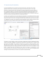
Figure 16 – iNemo M1 System-on-Board with the STM32 uC
To simulate the typical scenario for a small WSN the test device has been programmed to transmit small
data packets periodically in time: between two transmission different option of low power modes has been
explored. The power consumption of the entire system has been measured the voltage drop on a
small resistor (1Ohm) connected in series at the power supply cable.
The first two measures has been taken without using any power consumption technique. Both the
uC and the Spirit1 was configured to operate at the maximum allowed frequency (72 and 52Mhz
respectively). The radio output power level was set to 0dBm.
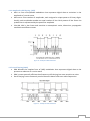
Wait for TX
Lock Tx
0dBm Tx Wait for next TX
Figure 17 – Power consumption with no low power techniques implemented
21
The upper signal shows the current absorbed by the TX nodes, the lower on has been used to
trigger the oscilloscope. The figure shows very clearly that when the radio module starts the
transmission operation (Lock TX) the power absorbed rise significantly and then go down a bit
during the transmission thanks to the low level used for the output. When the development
device is in idle the current absorbed is appreciably lower.
Table 2 – Power consumption with no low power modes (0dBm TX)
Wait for Tx
Lock Tx
0dBm Tx
Current
Time
Consumption Duration
35 mA
/
48 mA
550 us
46 mA
350 us
The next step has been to shut down the power module when not in transmission: the Spirit1 has been
switched off the the microcontroller has been configured in sleep mode (a very “light” low power mode
which allows a fast switch to the active one).
As you can see in the following images using low power techniques impact significantly on the
power consumption, especially when the device is in idle.
Note: starting from this test the transmission power level has been risen since the system was
much more efficient thanks to the power saved during the time spent in idle.
22
Figure 18 – STM32 Sleep Mode + Spirit1 Standby implementation
The current absorbed during idle has dropped from 34 to only 15mA for the entire system.
23
3.1 MCU in Standby Mode
An further step is to use a deeper sleep mode for the MCU: in this case the standby mode for the STM32
was used. Using the standby mode the device can achieve much lower level of absorbed current even if it
will need a reconfiguration after the wake-up and this imply a much longer delay before restart the
operation. However, if the idle time is order of magnitude greater than the activity time, the standby mode
is undoubtedly a better solution.
To wake-up the MCU the RTC alarm interrupt has been used: in this way no external interrupt is
necessary, all the peripherals can be switched off except the LSI (Low-Speed Internal) oscillator in
order to minimize the power consumption.
Wait for TX
Wait for TX
Wait for TX
Wait for TX
Figure 19 MCU Standby Mode
Current Consumption
MCU Sleep
MCU Standby
Idle Period
15 mA
1,735 mA
24
3.2 System battery life simulation
For actual embedded systems one of the most important parameters is the battery life in all that
applications which cannot use a different power supply. The instantaneous power is not the right
parameter to evaluate the battery life, the big deal is the energy requested by the system to perform a
task. The designer’s objective is to minimize this energy choosing the best combination between activity
time (generally inversely proportional to the energy), performance level and low power modes. If, for
example, the task is to monitor the temperature of a room to regulate radiators is sufficient to acquire few
data every 10 minutes using a deep low power state during the idle time.
To obtain a correct prediction of the system battery life is important to use simulations based on a system
characterization which provide the trend of the adsorbed power during the task of interest. In this chapter
the previous studies on the current consumption has been used to estimate the system autonomy using a
3.7V 1020mAh Li-Ion battery. The simulation has been developed using the Simulink environment and a
custom block has used to simulate a load with the same characteristic of the test system.
Figure 20 – Simulink block diagram utilized for the simulation of the battery life
Thinking at a system usable to acquire environment temperature the block simulating the device
under test has been configured to simulate the transmission of few data every 5 minutes using
high power level (10dBm). The simulation has been set to provide in output the battery status
after few hours of work. In order to have a short simulation time the final battery life as be
computed starting from the energy consumed in few hours. Since the time to simulate is long
(hours or better days) and the operation time, where the energy is concentrated, is very
concentrated (few micro seconds) the simulation steps have to be very small to have good results
making an eventual exhaustive simulation very expensive computationally.
25
Figure 21 – Result of the Simulink simulation
The simulation results shows that after an hour the battery charge level has a drop of 0,175%.
With a linear approximation the system, in this particular condition, would have a 24 days
autonomy.
26
Chapter 4: design of a PCB integrating the Spirit1 module
4.1 Idea
The dashboard electric system of the SCXV includes many different subsystems which all together assure
the communication between the steering wheel board and the other electronic parts of the car. In addition
the dashboard manages the 4.3” LCD display as well as some compulsory LEDs and some buttons. The goal
is to have a system capable to ensure that the driver has all the information he needs, with the possibility
to tune some key parameters (for example the amount of regenerative breaking torque) and have a
feedback when these changes are applied.
4.2 System Block Diagram
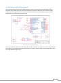
Figure 22 CXV Dashboard and Steering System block diagram
The electronic system is built around a main PCB (called “dashboard”) which you can see in the block
diagram above. On the electronic board there are the STM32 microcontroller (32 bit, based on ARM Cortex
M3 architecture), the high-speed CAN transceiver (AMIS−30663, fully compatible with the “ISO 11898−2”
standard) and all discrete components needed to supply the power to the system using the low voltage
battery as source. A series of Molex Microfit connectors are used to connect the electronic board to LEDs
and buttons on the dashboard, just in front of the driver. The connection with the LCD display is
implemented using the I2C protocol (using one of the two I2C peripheral of the STM32) . Finally the
connection with the steering-wheel electronic board is ensured by a Sub-GHz radio module, a
STMicroelectronics Spirit1, which allows a transfer rate up to 1Mb/s. A wired CAN bus connections is
available as radio backup together with an optional cabled power supply.
27
4.3 Schematic and PCB development
The schematic development began implementing the necessary components to made the MCU (Micro
Controller Unit) usable, which are the DC-DC converters (required to obtain the 3.3V and the 5V supply
voltages) and the programmer circuit (needed to download firmware inside the MCU using an external
programmer such as the ST-Link V2.0 we used).
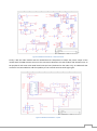
Figure 23 Dashboard Schematic - MCU
After that I added the CAN transceiver, the LCD connector (used for the I2C protocol and to supply power
to the display), the buttons connectors and another one used to read the output of an analog selector used
to manage different engine maps.
28
Figure 24 Dashboard Schematic – CAN and buttons
Finally I add the radio module and the needed discrete components to adapt the power output of the
module with the SMD antenna we used. The connections between the radio module and the MCU uses an
SPI peripheral and some other GPIO based interrupt lines (dedicated to the radio only). An additional UHF
connector has been added to add the capability to use external antennas with higher gain.
Figure 25 Dashboard Schematic – Spirit1
29
Since we used the OrCAD Capture tool to develop the schematic diagram, we rely on another Cadence CAD
for the layout of out PCBs, OrCAD Allegro PCB designer. Here is the layout of the dashboard PCB which
measures 140x100 mm.
Figure 26 Dashboard PCB
The datasheet of the antenna describes how to design the layout and the feeding line and also
STMicroelectronics gives advice about how to design the antenna circuit. Using the ‘’Cross-Section’’ tool
integrated in Cadence Allegro CAD is possible to calculate the geometrical parameters needed to obtain a
characteristic impedence equal to 50 Ohm.
Figura 27 - Allegro Cross-Section Tool
30
The antenna feeding line was designed in order to respect the design rules given by the antenna
manufacturer. The SMD passive components needed to couple correctly the antenna with the radio
module was placed in order to reduce as much as possible undesired parastitic effects.
Figura 28 – Feeding line layout and: in the upper picture the real PCB, in the lower one the CAD
31
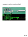
In the following image the placing of the most important components is shown.
• In red the microcontroller
STM32F103
• In white the power section,
with the 3.3V and the 5V
DC/DC
• In light blue the LCD
connector and the ones for
buttons and LEDs
• In blue the programming
connector and the CAN
controller section
• In violet the SPIRIT1 radio
(the antenna is on the top
rights corner)
Figure 29 - Dashboard PCB – Components layout
After the validation of this first PCB, which is actually only a prototype, another one has been developed
with a better components placing, an improved design of the radio circuit and with more available external
connectors: all this in a slightly smaller size.
Figure 30 Dashboard PCB – Version 2
32
References
“STM32F103xE” Datasheet, Doc ID 14611 Rev 7, 2009
“STM32F103xx” Reference Manual, Doc ID 13902 Rev 14, 2011
“Spirit1 Low data rate, low power sub-1GHZ transceiver” Datasheet, DocID022758 Rev 5,
2013
Mihail L. Sichitiu and Chanchai Veerarittiphan, “Simple, Accurate Time Synchronization for
Wireless Sensor Networks”, IEEE Wireless Communication and Networking, 2003, vol 2., pp.
1266-1273
“iNEMO system-on-board” Datasheet, DocID023268 Rev 1, 2013
“How to achieve the lowest current consumption with STM32F2xx” Application Note, Doc ID
019009 Rev 1, 2011
“Using the STM32 hardware real-time clock (RTC)” Application Note, Doc ID 018624 Rev 2,
2011
Dae-cheol You, Young-Si Hwang, Young-Ho Ahn, Ki-Seok Chung, “Energy Consumption
Prediction Technique for Embedded Mobile Device by Using Battery Discharging Pattern”,
Network Infrastructure and Digital Content, IEEE International Conference, 2010
“STM32 Nucleo boards” User Manual, DocID025833 Rev 2, 2014
“STM32L151xE and STM32L152xE” Datasheet, DocID025433 Rev 3, 2014
Some images by www.wikipedia.org
33


![Microsoft PowerPoint - 3110_f [Kompatibilit\344tsmodus]](http://vs1.manualzilla.com/store/data/006432867_1-0d15503617daa6b571ff8231a3e170df-150x150.png)