1
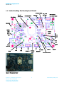
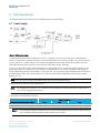
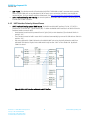
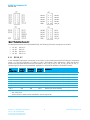
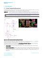
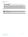
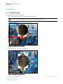
Bluetooth Low Energy (BLE) Development Kit User Manual Version 2.4 DVK-BL600-SA, DVK-BL600-SC, DVK-BL600-ST Americas: +1-800-492-2320 Option 2 Europe: +44-1628-858-940 Hong Kong: +852-2923-0610 www.lairdtech.com/bluetooth BL600 Development Kit Version 2.4 REVISION HISTORY Revision Date 1.0 22 Feb 2013 First Public Release 0 rev 1 PCB 2.0 11 April 2013 Technical and grammatical revisions for rev 02 PCB 2.1 5 July 2013 Changes Added: Section3.6, “OTA smart BASIC application download feature” Updated: Section 3.1 (Features) smart BASIC runtime engine FW upgrade capability Via UART (using the FTDI USB-UART). Changed: 2.2 20 Dec 2013 Section 0, nAutoRUN Pin and Operating Modes. To make it clear nAutoRUN pin control from PC (CON12 pin2-6 closed) or J6 (CON12pin2-6 open). Added Figure 6. 2.3 28 Jan 2014 Added Figure (Figure 2) to define correct ‘out of the box’ configuration settings. 2.4 01 May 2014 Updated Figure 2 (correct development board settings) to update the CON14 default settings. Americas: +1-800-492-2320 Option 2 Europe: +44-1628-858-940 Hong Kong: +852-2923-0610 www.lairdtech.com/bluetooth 2 CONN-GUIDE_BL600_DVK BL600 Development Kit Version 2.4 CONTENTS Revision History ...................................................................................................................................................... 2 Contents ................................................................................................................................................................ 3 1 Laird Bluetooth Low Energy Development Kit ..................................................................................................... 4 2 Overview ........................................................................................................................................................... 4 2.1 Introduction .............................................................................................................................................. 4 2.2 Package Contents ...................................................................................................................................... 4 3 BLE Development Kit – Main Development Board ............................................................................................... 5 3.1 Key Features .............................................................................................................................................. 5 3.2 Understanding the Development Board...................................................................................................... 6 4 Functional Blocks ............................................................................................................................................... 8 4.1 Power Supply ............................................................................................................................................ 8 4.2 4.1.1 Additional Power Option (for BL600 only) - Coin Cell .................................................................... 9 Reset Button .............................................................................................................................................. 9 4.3 JTAG Interface ........................................................................................................................................... 9 4.4 4-wire UART Serial Interface ...................................................................................................................... 9 4.5 4.4.1 UART Mapping ............................................................................................................................. 9 4.4.2 UART Interface Driven by USB ....................................................................................................... 9 4.4.3 UART Interface Driven by External Source .................................................................................... 10 nAutoRUN Pin and Operating Modes ....................................................................................................... 11 4.6 OTA (Over the Air) smart BASIC application download ............................................................................. 12 5 Software ......................................................................................................................................................... 12 6 Breakout Connector Pinouts ............................................................................................................................ 13 6.1 JP2, JP3, JP4, JP5 SIO (Special Input / Output Sockets) Breakout Connectors ............................................. 13 6.2 6.1.1 JP2 SIO_0-7 ................................................................................................................................ 14 6.1.2 JP3 SIO_8-15 .............................................................................................................................. 15 6.1.3 JP4 SIO_16-19 ............................................................................................................................ 15 6.1.4 JP5 SIO_21-30 ............................................................................................................................ 15 Additional Peripherals / Sensors ............................................................................................................... 16 6.2.1 Buzzer ........................................................................................................................................ 16 6.2.2 Temperature Sensor .................................................................................................................... 17 6.2.3 Trim Potentiometer ..................................................................................................................... 18 6.2.4 Push Buttons and LEDs................................................................................................................ 19 7 Other Features ................................................................................................................................................. 20 7.1 Current Consumption Measurement ........................................................................................................ 20 8 Additional Documentation ............................................................................................................................... 22 9 Appendix......................................................................................................................................................... 23 9.1 Coin Cell Insertion ................................................................................................................................... 23 9.2 Coin Cell Removal ................................................................................................................................... 24 Americas: +1-800-492-2320 Option 2 Europe: +44-1628-858-940 Hong Kong: +852-2923-0610 www.lairdtech.com/bluetooth 3 CONN-GUIDE_BL600_DVK BL600 Development Kit Version 2.4 1 LAIRD BLUETOOTH LOW ENERGY DEVELOPMENT KIT Part number: DVK-BL600-SA / DVK-BL600-SC / DVK-BL600-ST Applicable to the following BLE module part numbers: BL600-SA BL600-SC BL600-ST BL600 module featuring smart BASIC with integrated antenna BL600 module featuring smart BASIC with IPEX MHF4 connector BL600 module featuring smart BASIC with trace pads 2 OVERVIEW The Laird BLE development kit provides a platform for rapid wireless connectivity prototyping, providing multiple options for the development of Bluetooth Low Energy (BLE) applications. This manual is for Rev. 02 and later of the development PCB and relates to DVK-BL600-V02 and later on the PCB itself. The complete functionality of the development kit hardware requires the use of Laird BL600 series smart BASIC runtime engine FW version v1.1.50.0 or greater. 2.1 Introduction The Laird BLE development kit is designed to support the rapid development of applications and software for the BL600 series of BLE modules featuring Laird’s innovative event driven programming language – smart BASIC. More information regarding this product series including a detailed module User’s Manual and smart BASIC user guide is available on the Laird’s BL600 product pages. 2.2 Package Contents All kits contain the following items: Development Board Power Options The development board has the required BL600 module already soldered onto it and exposes all the various hardware interfaces available. USB cable – Type A to mini type B. The cable also provides serial communications via the FTDI USB – RS232 converter chip on the development board. DC barrel plug with clips for connection to external power supply Segger JTAG board – ‘jlink lite’ This third party JTAG interface provides the ability to upgrade the base firmware for the BL600 module. Additional details available at http://www.segger.com/cms/jlink-lite-cortexm.html Pin Headers x 4 Supplied to allow simple connection to SIO lines via the through hole plated areas JP2, JP3, JP4 and JP5. The headers are 2 x 5 way and are 2.54 mm pitch. IDC Cable x 4 Supplied to allow simple connection to the 2 x 5 way pin headers into JP2, JP3, JP4 and JP5. The IDC cables are 2.54 mm pitch. Provides links to additional information including the BL600 user manual, firmware, Laird BL600 app from the Apple app store, terminal utilities, schematics, quick start guides, and firmware release notes. Web link Card Americas: +1-800-492-2320 Option 2 Europe: +44-1628-858-940 Hong Kong: +852-2923-0610 www.lairdtech.com/bluetooth 4 CONN-GUIDE_BL600_DVK BL600 Development Kit Version 2.4 3 BLE DEVELOPMENT KIT – MAIN DEVELOPMENT BOARD This section describes the BL600 development board hardware. The BL600 development board is delivered with the BL600 series module loaded with integrated smart BASIC runtime engine FW but no onboard smart BASIC application; because of this, it starts up in AT command mode by default. smart BASIC applications are simple and easy to develop for any BLE application. Sample smart BASIC applications are available to download from the Laird BL600 product webpage or via the Laird global FAE network. The BL600 development board is a universal development tool to highlight the capabilities of the BL600 module. The development kit is supplied in a default configuration which should be suitable for multiple experimentation options. It also offers a number micro-DIP switches that help isolate on-board sensors and UART from the BL600 module to create different configurations. This allows you to test different operating scenarios. The development board allows the BL600 series module to physically connect to a PC via the supplied USB cable for development purposes. The development board provides USB-to-Virtual COM port conversion through a FTDI chip – part number FT232R. Any Windows PC (XP or later) should auto-install the necessary drivers; if your PC cannot locate the drivers, you can download them from http://www.ftdichip.com/Drivers/VCP.htm 3.1 Key Features The BL600 development board has the following features: BL600 series module soldered on-board. Power supply options for powering development board from: - USB - external DC supply - AAA batteries (3xAAA battery holder fitted on underside of development board) Regulated 3.3 V for powering the BL600 module. Optional regulated 1.8 V for powering the BL600 module. Power supply option for coin cell operation of the BL600 series module only (not development board). USB to UART bridge (FTDI chip). BL600 UART can be interfaced to: - USB (PC) using the USB-UART bridge - External UART source (using IO break-out connector when development board powered from DC jack) Current measuring (for BL600 module only) options: - Pin header (Ammeter) - Current shunt monitor IC (volt meter or oscilloscope) - Series resistor for differential measurement (oscilloscope) IO break-out (four 2x5-pin 2.54mm pitch headers) connectors interface for plugging-in external modules/sensors, and accessing all interfaces of the BL600 module [UART, SPI, I2C, SIO (DIO or AIN (ADCs)]. Two Buttons and two LEDs for user interaction. Two on-board sensors (analogue output): Temperature and Trim Pot. One buzzer. Micro DIP switches that allow the on-board sensors, LED’s (and USB UART FTDI bridge) to be disconnected from BL600 module. SMA connector (reverse SMA) for an external antenna. This is only applicable to BL600-ST module variant (with RF brought out to edge pads). smart BASIC runtime engine FW upgrade capability: - Via JTAG using the supplied Segger J-Link programmer - Via UART (using the FTDI USB-UART). smart BASIC application upgrade capability: - Via UART (using the FTDI USB-UART). Americas: +1-800-492-2320 Option 2 Europe: +44-1628-858-940 Hong Kong: +852-2923-0610 www.lairdtech.com/bluetooth 5 CONN-GUIDE_BL600_DVK BL600 Development Kit Version 2.4 3.2 Understanding the Development Board DIP switch CON13 Coin-cell FTDI-FT232R battery holder SIO_21-30 SIO_00-07 DIP switch CON14 JP5 UART Interface SMA Connector for BL600-ST Variant USB CON4 DC/USB Power Source Switch SW4 BL600-Sx Current Measurement module LED1 LED0 Button 1 DC Jack Input CN1 Buzzer SW5 SW6 Reset SW2 SIO_08-15 DIP Switch Con15 JTAG JP1 Button0 SIO_16-19 Current measurement Figure 1: Development board Americas: +1-800-492-2320 Option 2 Europe: +44-1628-858-940 Hong Kong: +852-2923-0610 www.lairdtech.com/bluetooth 6 CONN-GUIDE_BL600_DVK BL600 Development Kit Version 2.4 Important! To ensure correct ‘out of the box’ configuration, the BL600 development board must be set according to Figure 2. Figure 2: Correct development board settings Americas: +1-800-492-2320 Option 2 Europe: +44-1628-858-940 Hong Kong: +852-2923-0610 www.lairdtech.com/bluetooth 7 CONN-GUIDE_BL600_DVK BL600 Development Kit Version 2.4 4 FUNCTIONAL BLOCKS The development board is formed from the following major functional blocks: 4.1 Power Supply Figure 3: BL600 power supply The development board can be powered from 4.5-5.5 V supply (into DC jack connector CN1), 3xAAA batteries (holder J7 mounted on underside of board), or from the USB (type mini-B connector (CON4). The power source fed into DC jack (CN1) or 3xAAA batteries (J7) is combined together through diodes (diode-OR) and fed to the SW4 switch that allows selection of power source between either USB or the DC jack/AAA. The 5 V from the USB or the DC jack/AAA batteries is regulated down to 3.3 V with an on-board regulator on the development board. The CR2032 coin cell voltage is not regulated but is fed directly to BL600 module supply pin. Switch SW6 selects between the regulated 3.3 V and coin cell. Coin cell powers only the BLE600 module directly (on the development board, this is power domain VCC_nRF) and optionally (through R29) provides power to power domain VCC_IO. Note: The coin cell only powers the BL600 module and not the development board. Default position of SW5 is to select regulated 3.3 V. Note: The development board has a 1.8 V regulator for the possibility of powering the BL600 module from a 1.8 V rail (by changing SW5 position). The development board’s 3.3 V regulator provides power to the BLE module and USB UART bridge interface as well as to sensors on the development board. Development Board Power Source USB (CON4) Note 1 DC jack (CN1) or AAA battery (J7). Note 1: SW4 Position “USB” Position “DC” Switch Positions SW5 SW6 Position “3V3” always Position “3V3/1V8” Position “3V3” always Position “3V3/1V8”always The development board is powered from DC jack (or AAA batteries) when an external UART source is to be interfaced to BL600 module (using breakout connector JP5). Americas: +1-800-492-2320 Option 2 Europe: +44-1628-858-940 Hong Kong: +852-2923-0610 www.lairdtech.com/bluetooth 8 CONN-GUIDE_BL600_DVK BL600 Development Kit Version 2.4 On the development board, the power domain: VCC_nRF supplies the BL600 series module only. Current measuring block on development board only measures the current into power domain VCC_nRF. VCC_IO_UART supplies the FTDI chip IO and all other sensors and circuitry. VCC_IO is wired to the header connectors (JP2, JP3, JP4, JP5) via R29 and can be used to power external devices sensors. 4.1.1 Additional Power Option (for BL600 only) - Coin Cell The coin cell powers only the BLE600 module directly (on the development board, this is power domain VCC_nRF) and optionally (through R29) provides power to power domain VCC_IO. Refer to the Appendix for the correct method of coin cell insertion and removal. 4.2 Reset Button The development board has a reset button (SW2). The Reset is active low (SW2 pushed down). To view its location, refer to Figure 1. 4.3 JTAG Interface The development board has a 2-wire interface (JP1) which is used for BL600 series module smart BASIC runtime engine FW upgrade. To view its location, refer to Figure 1. 4.4 4-wire UART Serial Interface The development board provides access to the BL600 module 4-wire UART interface (TX, RX, CTS, RTS) either through USB (via U9 FTDI USB-UART convertor chip) or through a breakout header connector JP5. Refer to Figure 4. Note: BL600 module provides 4-wire UART interface on the HW and the other 4 signals (DTR, DSR, DCD, RI) which are low bandwidth signals can be implemented in a smart BASIC application, using any spare digital SIO pins. 4.4.1 UART Mapping UART connection on the BL600 series module and FTDI IC are shown in table below. Refer to Figure 4 to see how the BL600 series module UART is mapped to the breakout header connector (JP5). BL600 SIO SIO.21 SIO.22 SIO.23 SIO.24 BL600 Default function FTDI IC UART UART_TX (output) UART_RX (input) UART_RTS (output) UART_CTS (input) USB_RX USB_TX USB_CTS USB_RTS Additional SIO pins are also routed to the FTDI chip via a switch block. For example, the nAutoRUN input pin on the module can be driven by the DTR output pin of the FTDI chip. This allows testing the $autorun$ application on boot. 4.4.2 UART Interface Driven by USB USB Connector. The development kit provides a USB Type mini-B connector (CON4) which allows connection to any USB host device. The connector optionally supplies power to the development kit and the USB signals are connected to a USB to serial convertor device (FT232R), when SW4 is set to ‘USB’ position. Americas: +1-800-492-2320 Option 2 Europe: +44-1628-858-940 Hong Kong: +852-2923-0610 www.lairdtech.com/bluetooth 9 CONN-GUIDE_BL600_DVK BL600 Development Kit Version 2.4 USB – UART. The development kit is fitted with a (U9) FTDI FT232R USB to UART converter which provides USB-to-Virtual COM port on any Windows PC (XP or later). Upon connection, Windows auto-installs the required drivers. For more details and driver downloads, visit http://www.ftdichip.com/Products/FT232R.htm. UART interface driven by USB FTDI chip. In normal operation, the BL600 UART interface is driven by the FTDI FT232R USB to UART converter. 4.4.3 UART Interface Driven by External Source UART interface driven by external UART source. The BL600 module UART interface (TX, RX, CTS, RTS) is presented at a 2.54 mm (0.1”) pitch header (JP5). To allow the BL600 UART interface to be driven from the breakout header connector (JP5): - Development board must be powered from DC jack (CN1) or AAA batteries (J7) and switch SW4 is in position “DC”. The FTDI device must be held in reset which is achieved automatically by removal of USB cable or SW4 is in position “DC”. Also micro-DIP switch CON13 allows the four BL600 UART pins to be physically isolated as well from USB-UART FTDI device. Physical micro-DIP switch body has text “ON” on the closed side. By default CON13 is closed. Figure 4: USB to UART Interface and Header to UART interface Americas: +1-800-492-2320 Option 2 Europe: +44-1628-858-940 Hong Kong: +852-2923-0610 www.lairdtech.com/bluetooth 10 CONN-GUIDE_BL600_DVK BL600 Development Kit Version 2.4 4.5 nAutoRUN Pin and Operating Modes On the development board USB_DTR output (FTDI chip U9) from PC is wired to BL600 module pin SIO.28 (pin40) which is the nAutoRUN pin. Note: smart BASIC runtime engine FW checks for the status of nAutoRUN during power-up or reset. The nAutoRUN pin detects if the BL600 module should power up into “Interactive / Development Mode (3.3 V)” or “Self-contained Run Mode (0v)”. The module enters Self-contained Run Mode if the nAutoRUN pin is at 0V and an application called “$autorun$” exists in the modules file system, then the smart BASIC runtime engine FW will execute the smart BASIC application script automatically; hence the name Self-contained Run mode. The nAutoRUN pin inhibits the automatic launch $autorun$ application on power-up. Tying nAutoRUN to 3.3V inhibits the $autorun$ application from running. The J6 3-pin header allows a jumper to be fitted to select between the two operating modes. Note: Micro DIP switch CON12 pin2-6 MUST be open when using J6 3-pin header to select nAutoRUN function. Table 4-1: BL600 nAutoRUN pin nAutoRUN pin BL600 Operating Mode Interactive / Development Mode Self-contained Run Mode Circuit J6 jumper position Micro DIP switch CON12 allows the 4 x UART signals from the FTDI chip (USB_DSR, USB_DTR, USB_DCD, USB_RI) to be disconnected from reaching the BL600. By default the DIP switch is open. Since BL600 nAutoRUN pin40 (SIO.28) is connected to PC FTDI USB_DTR line, the Micro DIP switch: CON12 (pin 2-6) MUST be CLOSED (in ON position) to allow PC (using uWTerminal) to control nAutoRUN pin (SIO.28); with no jumper fitted to J6 (see Figure 5). CON12 (pin 2-6) MUST be OPEN to allow nAutoRUN pin (SIO.28) to be controlled by J6 (with jumper fitted to J6 pin1-2 to select nAutoRUN (see Figure 6). Figure 5: Micro DIP switch CON12 closed (nAutoRUN controlled by PC) Americas: +1-800-492-2320 Option 2 Europe: +44-1628-858-940 Hong Kong: +852-2923-0610 www.lairdtech.com/bluetooth 11 CONN-GUIDE_BL600_DVK BL600 Development Kit Version 2.4 Note: The additional lines of the DIP switch CON12 are not currently utilised and need to remain open, as shown in Figure 5. Figure 6: Micro DIP switch CON12 open (nAutoRUN controlled by J6 jumper on pin 1-2) 4.6 OTA (Over the Air) smart BASIC application download In a future release, it will be possible to download smart BASIC applications over the air with the BL600. this feature, SIO_7 must be pulled high externally. To enable On the development board, header connector JP2-pin 8 brings out the BL600 SIO_7; JP2-pin10 brings out VCC. To pull BL600 SIO_7 high (to VCC_IO), connect JP2-pin 8 to JP2-pin10 by fitting a jumper or fly-lead. Refer to latest FW release (v1_2_54_0-r2) documentation (FW release notes and smart BASIC user manual) for details. 5 SOFTWARE The development board connects the BL600 module to a virtual COM port of a PC or other device. From a PC, you can communicate with the module using Laird’s UW Terminal application (version 6.51 or newer). UW Terminal is a terminal emulation application capable of running on Windows 98, ME, 2000, XP, Windows 7, and Windows 8 operating systems. It was developed specifically to aid development and testing of Laird modules. It allows connection to serial devices using any combination of the communications parameters listed in Table 5-1. Table 5-1: Communication Parameters COM Port: 1 to 255 Baud rate: 300 to 921,600 Note: Baud rate default is 9600. Parity: None, Odd, Even Data Bits: 8 Stop Bits: 1 or 2 Handshaking: None or CTS/RTS Note: Baud rates higher than 115200 depend on the COM port capabilities of the host PC and may require an external USB – RS232 adapter or PCMCIA card. The benefits of using UW Terminal include: Continually displayed status of DSR, CTS, DCD, and RI Direct control of DTR on the host PC via a check box Direct control of RTS, if CTS / RTS Handshaking is disabled when UWTerminal is launched Sending of BREAK signals Americas: +1-800-492-2320 Option 2 Europe: +44-1628-858-940 Hong Kong: +852-2923-0610 www.lairdtech.com/bluetooth 12 CONN-GUIDE_BL600_DVK BL600 Development Kit Version 2.4 BASIC tab provides standalone testing and development of smart BASIC ** applications and allows UWTerminal operation to be automated. The BASIC embedded into UWTerminal, since version 6.20, shares the same core functionality as the BL600 series module. Additional built-in features (right click in Terminal tab screen) to accelerate development including Automation and various XCompile / Load / Run options for downloading smart BASIC applications into the BL600. Note: Full details on smart BASIC are available in the smart BASIC User Manual available for download at the Laird website. This document also includes a basic introduction to the UW terminal program. Tip: If the module returns a four hex digit error code: In UwTerminal, select those four digits, right-click, and select Lookup Selected ErrorCode. A description of the error is printed on screen. 6 BREAKOUT CONNECTOR PINOUTS 6.1 JP2, JP3, JP4, JP5 SIO (Special Input / Output Sockets) Breakout Connectors Access to all 28 BL600 series module signal pins (SIO’s = signal Input /Output) is available on four connectors JP2, JP3, JP4, JP5 (2.54 mm pitch 2x5 headers). Note: The BL600 module signal pins designation SIO (Signal Input /Output). DEFAULT type is DIO (Digital Input or Output) or UART (on fixed pins) ALTERNATE type is either AIN (Analog Input ADC), I2C, SPI, DIO (on fixed pins) Alternate function is selectable in smart BASIC application DIO or AIN functionality is selected using the GpioSetFunc() function in smart BASIC AIN configuration selected using GpioSetFunc() function I2C, UART, SPI controlled by xxxOPEN() functions in smart BASIC SIO_21 to SIO_24 are DIO by default when $autorun$ app runs on power up These breakout connectors can interface to a wide array of sensors with the BL600 function user configurable by smart BASIC application script from the default function (DIO, UART) to alternate functions (AIN (ADC), I2C, SPI, DIO). The BLE development kit incorporates additional connectors and cables inside the box, to enable simple, hassle-free testing of the multiple interfaces. Note: The orientation of the breakout connectors (shown in Figure 7) is viewed with the development board in a portrait position with the BL600 series module on the top edge. Americas: +1-800-492-2320 Option 2 Europe: +44-1628-858-940 Hong Kong: +852-2923-0610 www.lairdtech.com/bluetooth 13 CONN-GUIDE_BL600_DVK BL600 Development Kit Version 2.4 Figure 7: Breakout board connectors On development board version (DVK-BL600-V02), the following silk screen text appears on the PCB: For JP2 For JP3 For JP4 For JP5 SIO.01-07 SIO.8-15 SIO.16-19 SIO.21-30 6.1.1 JP2 SIO_0-7 In the smart BASIC application code written to use sensors on the development board (including the Temperature sensor - U1, Trim Pot - R9, Buzzer - U2, LED0 - D1, LED1 - D2, Button0 - SW1, and Button1 - SW3), the SIO pins direction and type (that these sensors are connected to, SIO_4, SIO_5, SIO_15, SIO_18, SIO_19, SIO_16, SIO_17 respectively) must be set in the smart BASIC application to override the defaults in the BL600 firmware. Pin Designation SIO_0 SIO_1 SIO_2 SIO_3 SIO_4 SIO_5 SIO_6 SIO_7 1 2 3 Default 1 Function DIO DIO DIO DIO DIO DIO DIO DIO Alternate 2 Function AIN AIN AIN AIN AIN AIN AIN Default 3 Direction Input Input Input Input Input Input Input Input Comment 8, 9, 10 bit resolution – voltage scaling 8, 9, 10 bit resolution – voltage scaling 8, 9, 10 bit resolution – voltage scaling 8, 9, 10 bit resolution – voltage scaling 8, 9, 10 bit resolution – voltage scaling 8, 9, 10 bit resolution – voltage scaling Internal pull down (default) DIO: Digital Input or Output AIN: Analog Input Default Direction In BL600 module smart BASIC runtime engine FW Americas: +1-800-492-2320 Option 2 Europe: +44-1628-858-940 Hong Kong: +852-2923-0610 www.lairdtech.com/bluetooth 14 CONN-GUIDE_BL600_DVK BL600 Development Kit Version 2.4 6.1.2 JP3 SIO_8-15 Pin Designation SIO_8 SIO_9 SIO_10 SIO_11 SIO_12 SIO_13 SIO_14 SIO_15 1 2 3 Default Function1 DIO DIO DIO DIO DIO DIO DIO DIO Alternate Function I2C_SDA I2C_SCL SPI_MOSI SPI_MISO SPI_CLK Default Direction3 Input Input Input Input Input Input Input Input Comment SPI_MOSI is an output in SPI master mode SPI_CLK is an output in SPI master mode Connects to BUZZER output on DVK DIO: Digital Input or Output AIN: Analog Input Default Direction In BL600 module smart BASIC runtime engine FW 6.1.3 JP4 SIO_16-19 Pin Designation SIO_16 SIO_17 SIO_18 SIO_19 1 2 3 Default Function1 DIO DIO DIO DIO Alternate Function Default Direction3 Input Input Input Input Comment Input for BUTTON 0 (SW1) on DVK Input to BUTTON 1 (SW3) on DVK Connects to LED 0 on DVK Connects to LED 1 on DVK DIO: Digital Input or Output AIN: Analog Input Default Direction In BL600 module smart BASIC runtime engine FW Note: SIO_20 is a No Connect (N/C) and is reserved by Laird for future use. 6.1.4 JP5 SIO_21-30 Pin Designation SIO_21 SIO_22 SIO_23 SIO_24 SIO_25 SIO_26 SIO_27 SIO_28 SIO_29 SIO_30 1 2 3 Default Function DIO DIO DIO DIO DIO NC NC nAutoRUN DIO DIO Alternate Function1 UART_TX UART_RX UART_RTS UART_CTS Default Direction3 Output Input Output Input Input Input ONLY Input Input Comment UART_DTR (CON12) on DVK DO NOT CONNECT DO NOT CONNECT UART_DSR (CON12) on DVK UART_DCD (CON12) on DVK UART_RI (CON12) on DVK DIO: Digital Input or Output AIN: Analog Input Default Direction In BL600 module smart BASIC runtime engine FW Americas: +1-800-492-2320 Option 2 Europe: +44-1628-858-940 Hong Kong: +852-2923-0610 www.lairdtech.com/bluetooth 15 CONN-GUIDE_BL600_DVK BL600 Development Kit Version 2.4 6.2 Additional Peripherals / Sensors The BLE development board provides for simple and hassle free connectivity to a wide range of sensors, but also includes several on-board sensors and options to enable a developer to test functionality straight out of the box. The additional peripherals and sensors on the development board can be isolated by micro-DIP switches CON14 and Temperature sensor CON15. Trim Pot (R9) (U1) DIP switch CON14 Buzzer (SP1) DIP switch Con15 Figure 8: BLE Development Board LED0 (D1) Button0 (SW1) Button1 (SW3 LED1 (D2) 6.2.1 Buzzer Figure 9: Buzzer The buzzer (U2) ACTC SMD PIEZO BUZZER part number APD-1203-PQ1 can be disconnected from BL600 module by micro-DIP switch CON15. Physical micro-DIP switch body has text “ON” on the closed side. To drive the buzzer, configure SIO_15 as a digital output using smart BASIC GpioSetFunc(15,2,0) and then, for example, write a 0 followed by a 1 to SIO_15 repeatedly in a loop. Americas: +1-800-492-2320 Option 2 Europe: +44-1628-858-940 Hong Kong: +852-2923-0610 www.lairdtech.com/bluetooth 16 CONN-GUIDE_BL600_DVK BL600 Development Kit Version 2.4 Sample smart BASIC applications are available from a Laird FAE, or refer to “bzt.buzzer.test.sb” in the smart BASIC sample application library on BL600 product pages at: http://lairdtech.com/Products/Embedded-Wireless-Solutions/Bluetooth-Radio-Modules/BL600-Series/ 6.2.2 Temperature Sensor Figure 10: Temperature Sensor The temperature sensor (U1) can be disconnected from BL600 module by micro-DIP switch CON14. Physical micro-DIP switch body has text “ON” on the closed side. The temperature sensor (U1) can be disconnected from supply rail by cutting the solder bridge SB1. The development board on-board temperature sensor (TI LM20BIM7 www.ti.com/lit/ds/symlink/lm20.pdf) has an Analogue output that is connected to BL600 module pin SIO_04; but since the LM20BIM7 has an analogue output, the BL600 module SIO-04 digital pin (DIO) must be configured as AIN analogue input (ADC). To configure the SIO_4 pin from DIO pin to Alternate function AIN, see file “ts.temperature.sensor.sb” in the smart BASIC sample application library on BL600 product pages at: http://lairdtech.com/Products/Embedded-Wireless-Solutions/Bluetooth-Radio-Modules/BL600-Series/. Key specifications of the LM20BIM7: Output type Accuracy at 30ºC Analogue output ±1.5ºC ±4ºC (max) Accuracy at 40ºC to +85ºC approx. ±2.5ºC ±5ºC (max) Power supply voltage range +2.4 V to 5.5 V Current Drain Output impedance 10 uA (max) 160 Ohms (max) LM20BIM7 datasheet states Temperature (T) to Voltage output (Vo) relationship approximated as a linear equation (for temperature range of -40ºC to +85ºC): Vo(mV) = -11.79mV/ºC x T + 1858.3 The table below gives below calculated Vo versus temperature: Temperature (T) +80ºC +70ºC +60ºC Typical Vo +924.7mV +1041.4mV +1158.1mV Americas: +1-800-492-2320 Option 2 Europe: +44-1628-858-940 Hong Kong: +852-2923-0610 www.lairdtech.com/bluetooth 17 CONN-GUIDE_BL600_DVK BL600 Development Kit Version 2.4 Temperature (T) +50ºC +40ºC +30ºC +20ºC +10ºC +0ºC -10ºC -20ºC -30ºC Typical Vo +1274.8mV +1391.5mV +1508.2mV +1624.9mV +1741.6mV +1858.2mV +1975.0mV +2091.7mV +2208.4mV 6.2.3 Trim Potentiometer The Trim Potentiometer is located in the middle of the development board to the right hand side of the coin cell holder. It is labelled ‘Trim Pot’ on the silkscreen. Figure 11: Trim Potentiometer The Trim Potentiometer (R9) can be disconnected from BL600 series module by micro-DIP switch CON14. Physical micro-DIP switch body has text “ON” on the closed side. The Trim Potentiometer (R9) can be disconnected from supply rail by cutting the solder bridge SB2. The Trim Potentiometer generates a voltage range of 0 V to ~0.9 V at C3 (CON14 pin3), see file tpt.trimpot.test.sb in the smart BASIC sample application library on BL600 product pages at http://lairdtech.com/Products/Embedded-Wireless-Solutions/Bluetooth-Radio-Modules/BL600-Series/. Americas: +1-800-492-2320 Option 2 Europe: +44-1628-858-940 Hong Kong: +852-2923-0610 www.lairdtech.com/bluetooth 18 CONN-GUIDE_BL600_DVK BL600 Development Kit Version 2.4 6.2.4 Push Buttons and LEDs Figure 12: Push buttons and LEDs The two push buttons and two LEDs on the DVK-BL600-V02 are connected to dedicated SIOs of the BL600 module. Part Button 0 (SW1) Button 1 (SW3) LED 0 (D1) LED 1 (D2) SIO SIO_16 SIO_17 SIO_18 SIO_19 If SIO_18 and SIO_19 are needed elsewhere, the LEDs can be disconnected by micro-DIP switch CON15. Physical micro-DIP switch body has text “ON” on the closed side. The buttons have no external pull-up resistor, so to use the buttons the SIO_16 and SIO_17 pins must be configured as an input with internal pull-up resistor. Example: A smart BASIC line that configures the pull-up. For further details see file “btn.button.led.test.sb” in the smart BASIC sample application library on BL600 product pages at http://lairdtech.com/Products/Embedded-Wireless-Solutions/Bluetooth-Radio-Modules/BL600-Series/. rc = GPIOSETFUNC(16,1,4): rc = GPIOSETFUNC(17,1,1): '//sets sio16 (Button0) as a digital in, strong pull up '//sets sio17 (Button1) as a digital in weak, pull down The LEDs are active high, meaning that writing a logical one (“1”) to the output pin illuminates the LED. One example of when push buttons can be used is when a smart BASIC application is written to simulate a generic data profile. Push buttons can then be pressed to increment or decrement, such as a heart rate. Americas: +1-800-492-2320 Option 2 Europe: +44-1628-858-940 Hong Kong: +852-2923-0610 www.lairdtech.com/bluetooth 19 CONN-GUIDE_BL600_DVK BL600 Development Kit Version 2.4 7 OTHER FEATURES 7.1 Current Consumption Measurement A removable jumper (CON1) is provided to break the power supply line directly to the module (if SB9 is cut), allowing you to measure current consumption. For normal operation, CON1 must be fitted. IMPORTANT: Note: To achieve the optimal power consumption of the BL600 series module on the development board, see the “LowPower.SB” file in the smart BASIC sample application library on BL600 product pages at http://lairdtech.com/Products/Embedded-Wireless-Solutions/Bluetooth-Radio-Modules/BL600-Series/. This only measures the current consumption of the BL600 series module ONLY. Figure 13: Current measurement Schematic and component location The current drawn by the BL600 series module can be monitored on the development board. Figure 13 shows the schematic (and location of measuring points on PCB) related to current measurements. To prepare the board for current measurement, cut the shorting of the solder bridge SB9. After this modification there are two primary ways to measure the current consumption: Using Ammeter – Connect an ampere meter between the two pins of connector CON1. This monitors the current directly. Using Oscilloscope (Note1) – Mount a resistor on the footprint R28. The resistor should not be larger than 10 Ohm. Connect an oscilloscope or similar with two probes on the pin on the CON1 connector and measure the voltage drop. The voltage drop is proportional with current consumption. If a 1 Ohm resistor is chosen, 1 mV equals 1mA. Americas: +1-800-492-2320 Option 2 Europe: +44-1628-858-940 Hong Kong: +852-2923-0610 www.lairdtech.com/bluetooth 20 CONN-GUIDE_BL600_DVK BL600 Development Kit Version 2.4 There is also a third way to measure current: Using Current Shunt Monitor – The current drawn by the BL600module can be monitored using the Current Shunt Monitor (CSM), INA216 (U8). The gain of INA216 is 200 V/V for lowest possible drop voltage. Note: The Using Current Shunt Monitor method allows the dynamic current consumption waveforms on oscilloscope as the BL600 radio operates. This can provide insight into power optimization. Current consumed by the BL600 series module is measured as a voltage (that is proportional to the current) using the CSM by connecting measuring voltmeter OR oscilloscope to TP14 Connect measuring voltmeter or oscilloscope GND to TP15. I(mA) = Vmeas_TP14(mV) /100 CAUTION: Take care not to short TP14 (the Current Shunt Monitor IC (U8)) output to GND, as that will permanently damage the IC U8. Americas: +1-800-492-2320 Option 2 Europe: +44-1628-858-940 Hong Kong: +852-2923-0610 www.lairdtech.com/bluetooth 21 CONN-GUIDE_BL600_DVK BL600 Development Kit Version 2.4 8 ADDITIONAL DOCUMENTATION Laird offers a variety of documentation and ancillary information to support our customers through the initial evaluation process and ultimately into mass production. Additional documentation includes: BL600 – smart BASIC User manual BL600 – smart BASIC sample applications library BL600 Firmware Upgrade Application note DVK-BL600 – User Manual DVK-BL600 - Schematics DVK-BL600 – Quick Start Guide for Heart Rate and Thermometer DVK-BL600 – Quick Start Guide for Proximity BL600 – User Manual – Hardware Datasheet and Integration Guide For any additional questions or queries, or to receive local technical support for this Development Kit or for the BL600 module series, please contact [email protected] Americas: +1-800-492-2320 Option 2 Europe: +44-1628-858-940 Hong Kong: +852-2923-0610 www.lairdtech.com/bluetooth 22 CONN-GUIDE_BL600_DVK BL600 Development Kit Version 2.4 9 APPENDIX 9.1 Coin Cell Insertion To insert the coin cell, follow these steps: 1. Push the coin cell against positive contact spring of holder J8. Note: The coin cell sits below the positive contact spring (as shown with arrow). Figure 14: Inserting the coin cell (step 1) 2. Push the coin cell down into the holder (J8). Figure 15: Inserting the coin cell (step 2) Americas: +1-800-492-2320 Option 2 Europe: +44-1628-858-940 Hong Kong: +852-2923-0610 www.lairdtech.com/bluetooth 23 CONN-GUIDE_BL600_DVK BL600 Development Kit Version 2.4 9.2 Coin Cell Removal To remove the coin cell, follow these steps: 1. Hold down the coin cell holder (J8) at the corners. 2. Use a screwdriver in the position shown in picture below, to gently remove the coin cell from the coin cell holder (J8), This is the correct method to remove coin-cell from holder (J8). Note: Due to tight fit of coin cell in the coin-cell holder (J8), care should be taken prevent damage to the J8 land pads. Figure 16: Removing the coin cell (step 2) CONN-GUIDE_DVK_BL600_v2.1 Copyright © 2013 Laird Technologies, Inc. All rights reserved. The information contained in this manual and the accompanying software programs are copyrighted and all rights are reserved by Laird Technologies, Inc. Laird Technologies, Inc. reserves the right to make periodic modifications of this product without obligation to notify any person or entity of such revision. Copying, duplicating, selling, or otherwise distributing any part of this product or accompanying documentation/software without the prior consent of an authorized representative of Laird Technologies, Inc. is strictly prohibited. All brands and product names in this publication are registered trademarks or trademarks of their respective holders. This material is preliminary Information furnished by Laird Technologies in this specification is believed to be accurate. Devices sold by Laird Technologies are covered by the warranty and patent indemnification provisions appearing in its Terms of Sale only. Laird Technologies makes no warranty, express, statutory, and implied or by description, regarding the information set forth herein. Laird Technologies reserves the right to change specifications at any time and without notice. Laird Technologies’ products are intended for use in normal commercial and industrial applications. Applications requiring unusual environmental requirements such as military, medical life-support or life-sustaining equipment are specifically not recommended without additional testing for such application. Limited Warranty, Disclaimer, Limitation of Liability Americas: +1-800-492-2320 Option 2 Europe: +44-1628-858-940 Hong Kong: +852-2923-0610 www.lairdtech.com/bluetooth 24 CONN-GUIDE_BL600_DVK