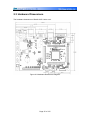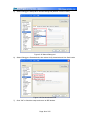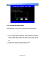
1
DevKit1207 Evaluation Kit 120MHz STM32F207IGT6 ARM Cortex-M3 32-bit Microcontroller CPU Internal 1MBytes of Flash and 128 +4 KBytes of SRAM 1 USB2.0 OTG Full-Speed port and 1 USB2.0 OTG High-Speed port 3.5’’ 240x320 TFT color LCD with 4-wire Resistive Touch Screen 10/100 Ethernet with IEEE 1588v2, CAN2.0B, IrDA, TF, Audio, JTAG Three axis linear accelerometer Supports for uC/OS-II and FreeRTOS Real-time Operating Systems User Manual COPYRIGHT DevKit1207 is trademarks of Embest Technology Co.,LTD. STM32F207, STM32 F217 are trademarks of STMicroelectronics Microsoft, MS-DOS, Windows XP are trademarks of Microsoft Corporation. Important Notice Embest has ownership and rights to the use of this document. Information in the document is within the protection of copyright. Unless specifically allowed, any part of this document should not be modified, issued or copied in any manner or form without prior written approval of Embest Technology Co., LTD. Page 1 of 155 Version of update records: Rev Date Description V1.0 2011-10-24 Initial version V1.1 2011-12-30 Added Appendix I Operation Notes Modified contents of Section 4.14 IWDG, Section 4.15 WWDG, Section 4.18.2 GSensor-LIS33DE to avoid ambiguity V1.2 2012-01-11 Added Appendix II PC-Development Platform Added step 7) in Section 3.4 Flash Loader V1.3 2012-04-06 Updated Figure 2-1 DevKit1207 Hardware Interface Diagram, Figure 2-2 Hardware Dimensions Diagram, Figure 3-15 Create New Project, Figure 3-19 Add file groups to project, Figure 3-21 Finish file groups adding, Figure 3-22 Add files to groups and Figure 3-24 Source flies have been added to groups. Added Section 3.2 IAR EWARM Added *.bin file support in Section 3.3 Flash Loader Page 2 of 155 Contact: If you want to order products from Embest, please contact Marketing Department: Tel: +86-755-25635656 / 25636285 Fax: +86-755-25616057 E-mail: [email protected] If you want to get technical assistance from Embest, please contact Technical Assistance Department: Tel: +86-755-25503401 E-mail: [email protected] URL: http://www.armkits.com Address: Room 509, Luohu Science &Technology Building, #85 Taining Road, Shenzhen, Guangdong, China (518020) Page 3 of 155 Contents Chapter 1 Overview ....................................................................................................... 9 1.1 Product introduction ....................................................................................... 9 1.2 Features ....................................................................................................... 11 1.3 Getting Started Quickly ................................................................................ 14 Chapter 2 2.1 CPU .............................................................................................................. 16 2.1.1 CPU Introduction .................................................................................. 16 2.1.2 CPU Features ....................................................................................... 16 2.2 Hardware interface....................................................................................... 17 2.2.1 Power Input Jack .................................................................................. 17 2.2.2 AUDIO OUTPUT Jack .......................................................................... 18 2.2.3 SPEAKER and CAN Interface .............................................................. 18 2.2.4 Serial Ports ........................................................................................... 18 2.2.5 Ethernet Interface ................................................................................. 19 2.2.6 JTAG Interface ...................................................................................... 19 2.2.7 MicroSD Card Interface ........................................................................ 20 2.2.8 Camera Interface .................................................................................. 21 2.2.9 USB OTG_FS Interface ........................................................................ 22 2.2.10 USB OTG_HS Interface ....................................................................... 22 2.2.11 TFT_LCD Interface ............................................................................... 23 2.2.12 LED ....................................................................................................... 24 2.2.13 KEY ....................................................................................................... 25 2.2.14 CAN-related Jumper ............................................................................. 25 2.2.15 BootLoader-related Jumpers ................................................................ 26 2.2.16 MicroSD Card, RS232 and IrDA related Jumpers ................................ 26 2.3 Chapter 3 3.1 Hardware System ....................................................................................... 16 Hardware Dimensions.................................................................................. 27 Software Development .............................................................................. 28 MDK-ARM .................................................................................................... 28 Page 4 of 155 3.1.1 MDK-ARM Introduction......................................................................... 28 3.1.2 Building an existing MDK-ARM Project ................................................ 30 3.1.3 Create a New MDK Project .................................................................. 36 3.2 IAR EWARM................................................................................................. 45 3.2.1 IAR EWARM Introduction ..................................................................... 45 3.2.2 Building an existing EWARM Project.................................................... 46 3.2.3 Create a New IAR Project .................................................................... 49 3.3 Flash Loader ................................................................................................ 55 Chapter 4 4.1 Peripheral’s Examples............................................................................... 61 Description of the Standard Peripherals Library .......................................... 62 4.1.1 Libraries folder ...................................................................................... 62 4.1.2 Project folder ......................................................................................... 63 4.1.3 Utilities folder ........................................................................................ 63 4.2 GPIO example.............................................................................................. 64 4.3 NVIC example .............................................................................................. 65 4.4 EXTI example............................................................................................... 67 4.5 DMA example ............................................................................................... 67 4.6 ADC example ............................................................................................... 69 4.7 DAC example ............................................................................................... 70 4.8 USART example .......................................................................................... 71 4.8.1 USART_Printf ....................................................................................... 71 4.8.2 USART_IRDA ....................................................................................... 72 4.9 PWR example .............................................................................................. 73 4.10 RCC example ............................................................................................... 74 4.11 RTC example ............................................................................................... 75 4.12 SysTick example .......................................................................................... 77 4.13 TIM example ................................................................................................ 78 4.14 4.13.1 PWM_Output example ......................................................................... 79 4.13.2 TimeBase .............................................................................................. 80 IWDG example ............................................................................................. 81 Page 5 of 155 4.15 WWDG example .......................................................................................... 82 4.16 CAN example ............................................................................................... 83 4.17 FLASH example ........................................................................................... 85 4.18 I2C example ................................................................................................. 85 4.18.1 EEPROM .............................................................................................. 86 4.18.2 GSensor-LIS33DE ................................................................................ 87 4.19 I2S example ................................................................................................. 88 4.20 SDIO example .............................................................................................. 89 4.21 LCD_Touch example.................................................................................... 90 4.22 CRC example ............................................................................................... 91 4.23 RNG_Touch example ................................................................................... 92 4.24 Lib_DEBUG example ................................................................................... 92 Chapter 5 Ethernet Demonstration ............................................................................ 94 5.1 Description of Ethernet Demonstration........................................................ 94 5.2 Standalone demos ....................................................................................... 98 5.2.1 HTTP server demo ............................................................................... 98 5.2.2 TFTP server demo .............................................................................. 100 5.2.3 TCP_echo_client demo ...................................................................... 102 5.2.4 TCP_echo_server demo..................................................................... 103 5.2.5 UDP_echo_client demo ...................................................................... 105 5.2.6 UDP_echo_server demo .................................................................... 106 5.3 FreeRTOS demos ...................................................................................... 108 5.3.1 HTTP server netconn demo ............................................................... 108 5.3.2 HTTP server_socket demo ................................................................. 110 5.3.3 UDP tcp_echo_server_netconn demo ............................................... 110 Chapter 6 USB Examples .......................................................................................... 111 6.1 Description of USB Examples.................................................................... 111 6.2 USB_Device_Examples ............................................................................. 113 6.2.1 USB AUDIO device example .............................................................. 114 6.2.2 USB DFU device example .................................................................. 116 Page 6 of 155 6.2.3 USB MSC device example ................................................................. 121 6.2.4 USB HID device example ................................................................... 123 6.2.5 USB DualCore device example .......................................................... 125 6.2.6 USB VCP device example .................................................................. 127 6.3 USB_Host example.................................................................................... 131 6.3.1 USB MSC host example ..................................................................... 132 6.3.2 USB HID host example ....................................................................... 136 6.3.3 USB DualCore host example.............................................................. 139 6.4 USB_Host_Device example ...................................................................... 141 Chapter 7 uC/OS-II & uC/GUI Demo ......................................................................... 144 Chapter 8 G-Sensor Demonstration ........................................................................ 145 Chapter 9 Various Other Tests Scenario ................................................................ 147 9.1 LED and Key Testing ................................................................................. 147 9.2 ADC Testing ............................................................................................... 147 9.3 DAC Testing ............................................................................................... 147 9.4 USART Testing ........................................................................................... 147 9.5 IRDA Testing .............................................................................................. 147 9.6 CAN Testing ............................................................................................... 147 9.7 I2S Testing ................................................................................................. 147 9.8 MicroSD Card Testing ................................................................................ 147 9.9 RTC Testing................................................................................................ 148 9.10 Ethernet Testing ......................................................................................... 148 9.11 USB Testing ............................................................................................... 148 9.12 LCD_Touch Testing .................................................................................... 148 9.13 Camera Testing .......................................................................................... 148 Chapter 10 What’s in the BOX .................................................................................... 149 Appendix I Operation Notes ......................................................................................... 150 Appendix II PC-Development Platform ........................................................................ 151 Technical support & Warranty Service ........................................................................ 152 Technical support service ......................................................................................... 152 Page 7 of 155 Maintenance service clause ..................................................................................... 153 Basic notice to protect and maintenance LCD ......................................................... 154 Value Added Services............................................................................................... 154 Page 8 of 155 Chapter 1 Overview 1.1 Product introduction The STMicroelectronics‟ STM32F207IGT6 flash microcontroller is from STM32F207xx family, which is based on the high-performance ARM Cortex-M3 32-bit RISC core operating at a frequency of up to 120MHz, with high-speed embedded memories (1Mbytes of flash memory and 128Kbytes of system SRAM), 4Kbytes of backup SRAM, 2Kbits EEPROM and powerful peripheral functions, including digital camera module interface, High-speed USB OTG, Full-speed USB OTG, Ethernet MAC, CAN2.0B, multiple timers, ADCs and DACs, I2C, I2S, SPI, UARTs/USARTs, SDIO, LCD interface, RTC and programmable IOs. Embest DevKit1207 Evaluation Kit is a complete development platform for STM32F207IGT6 devices which enables engineers to easily and rapidly evaluate, prototype and test designs built around the STMicroelectronics STM32F207xx series microcontrollers. The DevKit1207 board has exposed a full range of hardware peripherals to support HS/FS USB OTG, Ethernet, CAN, Camera, Serial port, IrDA, TF card, LCD, Touch screen, Audio, G-sensor, RTC, JTAG, etc. The kit is provided with an industrial-level 3.5 inch LCD screen. In addition Embest has ported uC/OS-II and uC/GUI on this board. Embest also has ported FreeRTOS real-time operating system for LwIP ethernet applications. Embest provides the uC/OS-II BSP, FreeRTOS source code and plenty of software examples, board schematic and user manual to help customer better understanding this board and make development based on this borad easier. Note: You are required to purchase a license for use uC/OS-II and uC/GUI in any commercial application Page 9 of 155 DevKit1207 can be used in the following applications: Industrial Control Medical Equipment Home Automation Human Interface Consumer Electronics Test and Measurement DevKit1207 Function Block Diagram Figure 1-1 DevKit1207 Function Block Diagram Page 10 of 155 1.2 Features DevKit1207 evaluation board is based on STM32F207IGT6 microcontroller and it integrates all the functions and features of this IC‟s. The features of this board are as follows: Processor STMicroelectronics STM32F207IGT6 Flash Microcontroller ARM 32-bit Cortex-M3 CPU with ART accelerator, frequency up to 120MHz Onchip 1Mbytes of Flash memory and 128+4Kbytes of SRAM Flexible static memory controller that supports Compact Flash, SRAM, PSRAM, Nor and Nand memories LCD parallel interface, 8080/6800 modes USB 2.0 High-Speed/Full-Speed Device/Host/OTG 10/100 Ethernet MAC, supports IEEE 1588v2 hardware, MII/RMII 2 CAN 2.0B interfaces;up to 4 USARTs and 2 UARTs, 3 SPI (30Mbit/s), 2 with muxed I2S 8- to 14-bit parallel camera interface (up to 48Mbytes/s) 1-/4-/8-bit SD/MMC/SDIO interface, supports up to 32Gbytes storage Up to 140 I/O ports up to 60MHz Up to 17 timers (two 32-bit timers), up to 120MHz 3 x 12-bit A/D converters, 2 x 12-bit D/A converters Analog true random number generator Low power, supports Sleep, Stop and Standby modes Supports booting from Flash, System memory or SRAM Supports ISP and IAP programming External Memory Onboard I2C compatible serial interface 2Kbits EEPROM Micro SD card slot Page 11 of 155 Audio interfaces 1 x stereo headphone output jack 1 x speaker output jack 1 x audio DAC output jack LCD/Touch Screen 3.5 inch TFT color LCD (240 x 320-pixel RGB resolution, 262000 colors, 16-bit 8080 parallel interface, brightness control via PWM) 4-wire resistive touch screen Data Transfer Interfaces 1 x 5-wire RS232 Serial Port 1 x USB2.0 OTG/Device/Host, High-speed, up to 480Mbps 1 x USB2.0 OTG/Device/Host, Full-speed, up to12Mbps 1 x 10/100 Ethernet with IEE 1588v2 (RJ45 connector) 1 x CAN2.0B interface 1 x IrDA transceiver Input Interface and Other Facilities 1 x Camera interface 1 x Potentiometer (A/D converter) 2 x USER buttons 1 x RESET button 1 x WAKEUP button 20-pin standard JTAG interface RTC battery socket (User needs to prepare battery, CR1220 model is recommended) 1 x LED for Power indicator 2 x LEDs for USB OTG FS indicators 2 x LEDs for USB OTG HS indicators 4 x User LEDs 140 GPIO pins are all brought out Page 12 of 155 Mechanical Parameters Dimensions: 160 mm x 115 mm Input Voltage: +5V Power consumption: 0.4A@5V Working Temp.: -10 ℃ ~ 70 ℃ Humidity Range: 20% ~ 90% Page 13 of 155 1.3 Getting Started Quickly This section will tell the user how to understand and use DevKit1207 better and faster. For more information please refer to the listed document and location. For hardware development: Hardware system Introduce CPU, expanded chip and hardware interface User Manual->2 Hardware System CPU Datasheet Know principle and configuration of STM32F2xx CD->\HW design\datasheet\CPU\ Schematic diagram of DevKit1207 Know hardware principle of DevK1207 CD->\HW design\schematic Dimensional drawing of DevKit1207 Refer to the actual length and height of DevKit1207 to bring convenience for opening die User Manual->2.3 Hardware Dimensions For software development: Establish developing and compilation environment Software development Test functionality of interface Building and instructions for MDK-ARM IDE User Manual->3 Software Development Standard peripherals driver example and how to proceed User Manual ->4 Peripheral‟s Examples Introduction for Ethernet drivers and applications User Manual ->5 Ethernet Demonstration Introductions for USB applications and development User Manual ->6 USB Examples Introduction for migration and development of uCos-II & ucgui User Manual ->7 uCos-ii & ucgui example Introductions for G-Sensor application User Manual ->8 G-Sensor application Documentation and reference manuals for software development CD-ROM ->\STM32F2x_Software_ programing_manual CD-ROM ->\STM32F2xx_Application note Test the interface of the board carrier User Manual-> 9 Various Tests senario Page 14 of 155 For marketing: Hardware CPU feature, board carrier User Manual->1.1 Product introduction system interface data User Manual->1.2 Features Dimensional Refer to the actual length and drawing of height of DevKit1207 to bring DevKit1207 convenience for opening die User Manual->2.3 Hardware Dimensions For learning personnel: It is suggested to browse each section in each chapter of this Manual in order. Page 15 of 155 Chapter 2 Hardware System 2.1 CPU 2.1.1 CPU Introduction The ARM Cortex™-M3-based STM32 F2 series is built on ST‟s advanced 90 nm NVM process technology with the innovative Adaptive Real-Time memory accelerator (ART Accelerator™) and the multi-layer bus matrix offering an unprecedented price/performance trade-off. 2.1.2 CPU Features STM32F207IGT6 is characterized by a high degree of integration combining 1 Mbyte of Flash memory and 128 Kbytes of SRAM with Ethernet MAC, USB 2.0 HS OTG, camera interface, and hardware encryption support and external memory interface. ST„s acceleration technology enables STM32 F2 MCUs to achieve up to 150 DMIPS at 120 MHz CPU which is equivalent to zero wait state execution, while keeping the dynamic current consumption with 188 µA/MHz at an outstandingly low level. Page 16 of 155 2.2 Hardware interface Figure 2-1 DevKit1207 Hardware Interface Diagram The following section gives in detail about the pin numbers and its function description of various different IC‟s blocks present in DevKit1207. 2.2.1 Power Input Jack Table 2-1 Power Input Jack J1 Pin Signal Description 1 GND GND 2 GND GND 3 +5V Power supply(+5V) 2A (Type) Page 17 of 155 2.2.2 AUDIO OUTPUT Jack Table 2-2 AUDIO OUTPUT Jack J2 Pin Signal Description 1 GND GND 2 Left Left output 3 Right Right output 4 Right Right output 5 Left Left output 2.2.3 SPEAKER and CAN Interface Table 2-3 SPEAKER and CAN Interface CON5 Pin Signal Description 1 CAN1_L Low-level CAN bus line 2 CAN1_H High-level CAN bus line 3 SPK_OUT+ PWM Speaker Output positive 4 SPK_OUT- PWM Speaker Output negative 2.2.4 Serial Ports Table 2-4 Serial Ports Interface COM1 Pin Signal Description 1 NC NC 2 RXD Receive data 3 TXD Transit data 4 NC NC 5 GND GND Page 18 of 155 6 DSR Data Set Ready 7 NC NC 8 CTS Clear To Send 9 NC NC 2.2.5 Ethernet Interface Table 2-5 Ethernet Interface CON1 Pin Signal Description 1 TX+ TX+ output 2 TX- TX- output 3 VDD3V3 3.3V Power for TX/RX 4 4&5 Connect to Shelter 5 7&8 Connect to Shelter 6 VDD3V3 3.3V Power for TX/RX 7 RX+ RX+ input 8 RX- RX- input 9 LED1 Speed LED 10 VDD3V3 3.3V Power for LED 11 LED2 Link LED 12 VDD3V3 3.3V Power for LED 13 GND GND 14 GND GND 15 NC NC 16 NC NC 2.2.6 JTAG Interface Page 19 of 155 Table 2-6 JTAG Interface CON12 Pin Signal Description 1 VTREF +3.3V power supply 2 VSUPPLY +3.3V power supply 3 NTRST Test system reset 4 GND GND 5 TDI Test data input 6 GND GND 7 TMS Test mode select 8 GND GND 9 TCK Test clock 10 GND GND 11 RTCK GND 12 GND GND 13 TDO Test data output 14 GND GND 15 NSRST Test system reset 16 GND GND 17 DBGRQ Connect to GND 18 GND GND 19 DBGACK Connect to GND 20 GND GND 2.2.7 MicroSD Card Interface Table 2-7 MicroSD Card Interface CON4 Pin Signal Description 1 DAT2 Card data 2 Page 20 of 155 2 DAT3 Card data 3 3 CMD Command Signal 4 VDD VDD 5 CLK Clock 6 VSS VSS 7 DAT0 Card data 0 8 DAT1 Card data 1 9 CD Card detect 2.2.8 Camera Interface Table 2-8 Camera Interface CON6 Pin Signal Description 1 GND1 GND 2 D0 NC 3 D1 NC 4 D2 Digital image data bit 0 5 D3 Digital image data bit 1 6 D4 Digital image data bit 2 7 D5 Digital image data bit 3 8 D6 Digital image data bit 4 9 D7 Digital image data bit 5 10 D8 Digital image data bit 6 11 D9 Digital image data bit 7 12 D10 NC 13 D11 NC 14 GND2 GND 15 PCLK Pixel clock 16 GND3 GND Page 21 of 155 17 HS Horizontal synchronization 18 VDD50 NC 19 VS Vertical synchronization 20 VDD33 +3.3V 21 XCLKA Clock output a 22 XCLKB NC 23 GND4 GND 24 FLD NC 25 PWR_EN Power Enable 26 RST Reset the camera 27 SDA I2C master serial clock 28 SCL I2C serial bidirectional data 29 GND5 GND 30 VDDIO +3.3V 2.2.9 USB OTG_FS Interface Table 2-9 USB OTG_FS Interface CON2 Pin Signal Description 1 VBUS +5V 2 D- USB Data- 3 D+ USB Data+ 4 ID USB ID 5 GND GND 2.2.10 USB OTG_HS Interface Table 2-10 USB OTG_HS Interface CON3 Pin Signal Description Page 22 of 155 1 VBUS +5V 2 D- USB Data- 3 D+ USB Data+ 4 ID USB ID 5 GND GND 2.2.11 TFT_LCD Interface Table 2-11 TFT_LCD Interface CON7 Pin Signal Description 1 VDD5 +5V 2 VDD5 +5V 3 GND GND 4 GND GND 5 VDD33 +3.3V 6 VDD33 +3.3V 7 LCD_PWM LED Dimming Control by PWM Signal 8 I2C_SCL I2C master serial clock 9 I2C_SDA I2C serial bidirectional data 10 TC_INT Touch screen interrupt 11 LCD_RST LCD reset 12 LCD_cs LCD chip select 13 GND GND 14 GND GND 15 GND GND 16 D0 16-bit 8080 parallel interface, Data bit 0 17 D1 16-bit 8080 parallel interface, Data bit 1 18 D2 16-bit 8080 parallel interface, Data bit 2 19 D3 16-bit 8080 parallel interface, Data bit 3 Page 23 of 155 20 D4 16-bit 8080 parallel interface, Data bit 4 21 D5 16-bit 8080 parallel interface, Data bit 5 22 GND GND 23 D6 16-bit 8080 parallel interface, Data bit 6 24 D7 16-bit 8080 parallel interface, Data bit 7 25 GND GND 26 D8 16-bit 8080 parallel interface, Data bit 8 27 D9 16-bit 8080 parallel interface, Data bit 9 28 D10 16-bit 8080 parallel interface, Data bit 10 29 D11 16-bit 8080 parallel interface, Data bit 11 30 D12 16-bit 8080 parallel interface, Data bit 12 31 D13 16-bit 8080 parallel interface, Data bit 13 32 D14 16-bit 8080 parallel interface, Data bit 14 33 D15 16-bit 8080 parallel interface, Data bit 15 34 GND GND 35 GND GND 36 GND GND 37 LCD_DC LCD Parallel Interface 38 LCD_RD Read signal 39 LCD_WR Write signal 40 GND GND 2.2.12 LED Table 2-12 LEDs LED 1~9 LED Signal Description LED1 3V3 3.3V power indicator LED 2 VBUS_FS USB_FS indicator 1 LED 3 3V3 USB_FS indicator 2 Page 24 of 155 LED 4 VBUS_HS USB_HS indicator 1 LED 5 3V3 USB_HS indicator 2 LED 6 PC.07 User-defined LED 1 LED 7 PG.08 User-defined LED 2 LED 8 PG.06 User-defined LED 3 LED 9 PD.12 User-defined LED 4 Note: There is a simple one to one relationship between LED1~LED4 in software and LED6~LED9 in hardware 2.2.13 KEY Table 2-13 KEYs SW2~SW5 Key Signal Description SW2 RESET System reset key SW3 WAKE_UP System wake up key SW4 USER1 User-defined key 1 SW5 USER2 User-defined key 2 2.2.14 CAN-related Jumper Table 2-14 CAN-related Jumper JP9 Jumper Description To enable the terminal resistor for the selected CAN, fit a JP9 jumper on JP9. Default setting: Fitted Note: JP9 should be fitted in order to enable CAN working properly. Page 25 of 155 2.2.15 BootLoader-related Jumpers Table 2-15 BootLoader-related Jumpers JP1 & JP2 Jumper Description Bootloader_BOOT0 is managed by pin 6 of COM1 (RS-232 DSR signal) when JP1 is closed. This configuration is used JP1 for boot loader application only. Default setting: Not fitted. Bootloader_RESET is managed by pin 8 of COM1 (RS-232 CTS signal) when JP2 is fitted. This configuration is used JP2 for boot loader application only. Default setting: Not fitted. Note: JP1 and JP2 should be kept not fitted if you don’t use BootLoader function. 2.2.16 MicroSD Card, RS232 and IrDA related Jumpers Table 2-16 MicroSD Card, RS232 and IrDA related Jumpers JP5 & JP6,JP7 & JP9,JP10 & JP11 Jumper Group1 Description JP5 When JP5 and JP6 fitted, PC10·and PC11are JP6 connected to DATA2 and DATA3 pins of MicroSD Card. Group2 Group3 JP7 When JP7 and JP8 fitted , PC10·and PC11are JP8 connected to TX and RX pins of MAX3243. JP10 When JP10 and JP11 fitted,PC10·and PC11are JP11 connected to TX and RX pins of TFDU6300. Note: There should be just one group of jumpers fitted at the same time. If more than one group of jumpers is fitted, some device may not work properly. Page 26 of 155 2.3 Hardware Dimensions The hardware dimensions of DevKit1207 (Units: mm): Figure 2-2 Hardware Dimensions Diagram Page 27 of 155 Chapter 3 Software Development There are two main software development environments for STM32F2xx series MCU, Keil MDK-ARM and IAR EWARM. The following sections will give a short description of these software and show how to use them. 3.1 MDK-ARM 3.1.1 MDK-ARM Introduction The MDK-ARM is a complete software development environment for Cortex™-M, Cortex-R4, ARM7™ and ARM9™ processor-based devices. MDK-ARM is specifically designed for microcontroller applications, it is easy to learn and use, yet powerful enough for the most demanding embedded applications. Features Complete support for Cortex-M, Cortex-R4, ARM7, and ARM9 devices Industry-leading ARM C/C++ Compilation Toolchain µVision4 IDE, debugger, and simulation environment Keil RTX deterministic, small footprint real-time operating system (with source code) TCP/IP Networking Suite offers multiple protocols and various applications USB Device and USB Host stacks are provided with standard driver classes Complete GUI Library for embedded systems with graphical user interfaces ULINKpro enables on-the-fly analysis of running applications and records every executed Cortex-M instruction Complete Code Coverage information about your program's execution Execution Profiler and Performance Analyzer enable program optimization Numerous example projects help you quickly become familiar with MDK-ARM's powerful, built-in features CMSIS Cortex Microcontroller Software Interface Standard compliant Page 28 of 155 The following block diagram illustrates the complete µVision4 software development cycle. Figure 3-1 Software development cycle The STM32F2xx series MCUs require MDK4.20 and later versions. The demo version of MDK4.22a with code limitation is supplied along with the kit in CD-ROM. User need to purchase or get the license themselves in order to use MDK-ARM software without any code limitations. All MDK projects under folder \MDK-ARM in the CD-ROM are built with MDK4.22a. The sections Building an existing MDK-ARM Project and Create a New MDK Project give a short description of how to use the MDK-ARM to develop application software. For more detail, please refer to the relevant documentation. Page 29 of 155 3.1.2Building an existing MDK-ARM Project In this section, ADC3_DMA as an example has been used to show how to configure an existing MDK project. 1) Open project. Open the ADC3_DMA project from the directory as follow. code\STM32F2xx_StdPeriph_Demo\Project\STM32F2xx_StdPeriph_Examples\ADC\ ADC3_DMA\MDK-ARM Click the icon to configure “Target options” as show in following picture. Figure 3-2 Configure Target options 2) In the opened window, select the "Device" tab, and select the MCU from the list, as shown below: Figure 3-3 Select the MCU model 3) Select the "Output" tab if you want to MDK output HEX file, and select “Create HEX File”. Page 30 of 155 Figure 3-4 Select output file 4) Select the “Debug” tab to choose Debug tool. If you want to use ULINK, select “ULINK Cortex Debugger” (Default setting). Figure 3-5 Select ULINK as Debug tool If you want to use JLINK, select “Cortex-M/R J-LINK/J-Trace”. Page 31 of 155 Figure 3-6 Select JLink as Debug tool Click “Settings” to setup JLink. The “Max Clock” is suggested to be lower than 2MHz.Click”OK”, return to “Debug” window. Figure 3-7 JLink settings 5) Select “Utilities” tab to setup Flash Programming. Page 32 of 155 If you want to download programs with ULINK, please select “ULINK Cortex Debugger” (Default Setting).As shown in following figure. Figure 3-8 Select ULINK as program downloader If you want to download programs with JLink, please select “Cortex-M/R J-LINK/J-Trace”. Figure 3-9 Select JLink as program download tool Page 33 of 155 6) Click “Settings” to configure Flash download. If you want MCU to reset and run automatically after Flash downloading, please select “Reset and Run” option. Figure 3-10 Flash download settings 7) Click “Add” to add programming algorithm. Select “STM32F2xx Flash On-chip Flash 1M” algorithm, and then click “Add”. Figure 3-11 Add programming algorithm Page 34 of 155 8) Click “OK” to finish the setup and return to IDE window. Figure 3-12 Finish target option setup 9) Click “Build” or “Rebuild” to build or rebuild the project. Figure 3-13 Build or Rebuild the project 10) Click “Download” to download program to MCU. Figure 3-14 Download program 11) If you have selected “Reset and Run” option in step 6), MCU will reset and run automatically after downloading. If haven‟t, you just need to press the Reset key on the Evaluation board to run the MCU. Page 35 of 155 3.1.3 Create a New MDK Project This section shows how to create a new project with MDK-ARM. 1) Open the directory of \code\STM32F2xx_StdPeriph_Demo .Create a new folder and name it „My project‟. Create a new folder in \My Project and name it, such as ADC_example. Copy source files and include files from the specified example, for example ADC3_DMA, to the folder \ADC_example created in previous step. main.c stm32f2xx_it.c stm32f2xx_it.h system_stm32f2xx.c stm32f2xx_conf.h 2) Open MDK (KEIL µVision4). Click “Project”->”New uVision Project”. Figure 3-15 Create New Project Save the project in the folder of \ADC_example as ADC_example. Page 36 of 155 Figure 3-16 Save project 3) Then a dialog box of “Select Device for Target of Target …” will be opened. Please select a device for the project. Here we select “STM32F207IG”. Figure 3-17 Select the MCU model 4) A dialogue box pops up to ask if you want to add Startup code to project. The Startup Code performs configuration of the microcontroller device and Page 37 of 155 initialization of the compiler run-time system. You can select “Yes”, uVision will add it for you, or “No” then you need to add it by yourself. Here we select “NO” and add it later. Figure 3-18 Add startcode 5) Now add file groups to project. Right click on “Target”, select “Add Group…” and name the file group. Figure 3-19 Add file groups to project Select “Manage Components” and click icon to create new file group as shown in the figure below. Page 38 of 155 Figure 3-20 Add file groups to project with Manage Components 6) Create 5 file groups as shown: User, Lib, STM32_EVAL, CMSIS, and MDK-ARM. As shown below: Figure 3-21 Finish file groups adding Note: File groups are used to manage files of project. 7) User Group: manage source files that user create Lib Group: manage STM32F2xx Standard Peripherals Library STM32_EVAl: manage board driver CMSIS: manage CMSIS files MDK-ARM: manage StartUp code Add files to groups. Right Click on group of User, select “Add files to Group „User‟...” Page 39 of 155 Figure 3-22 Add files to groups Add files from the created folder \My Project\ADC_example to the group of „User‟. Figure 3-23 Add selected files to group 8) Add files to the group of Lib, STM32_EVAL, CMSIS, and MDK-ARM same as done in step 7). The files need to be added to the group of Lib are located in \code\STM32F2xx_StdPeriph_Demo\Libraries\STM32F2xx_StdPeriph_Driver\src Note: Only related files need to be added. If you are unsure what files should be added, you can add all files to group of Lib. However, it will increase compile Page 40 of 155 time and code size. The files need to be added to the group STM32_EVAL are located in \code\STM32F2xx_StdPeriph_Demo\Utilities\STM32_EVAL\STM322xG_EVAL Note: Only stm322xg_eval.c and stm322xg_eval_lcd.c need to be added to group of STM32_EVAL. The files need to be added to the group CMSIS are located in \code\STM32F2xx_StdPeriph_Demo\Libraries\CMSIS\CM3\CoreSupport Note: Only core_cm3.c need to be added to group of CMSIS. The files need to be added to the group MDK-ARM are located in \code\STM32F2xx_StdPeriph_Demo\Libraries\CMSIS\CM3\DeviceSupport\ST\STM3 2F2xx\startup\arm Note: Only startup_stm32f2xx.s need to be added to group of MDK-ARM. As the figure shown below, required source flies have been added to the groups. Figure 3-24 Source flies have been added to groups Page 41 of 155 9) Setup Target options. Click the icon “Target Options”,select „C/C++‟ tab to set C/C++ compiler specific tool options like code optimization or variable allocation. Figure 3-25 Setup Target options There are two options we have to set. Figure 3-26 C/C++ option 10) Add Preprocessor Symbols. As several preprocessor symbols have been defined in project, we need to add them to the column of „Define‟. Page 42 of 155 Figure 3-27 Add Preprocessor Symbols 11) Add Include Paths. Click the icon shown in the figure below. Figure 3-28 Include Paths option In „Folder Setup‟ dialog box, click icon shown below and add Include Paths. Page 43 of 155 Figure 3-29 Add Include Paths Include Paths have been setup as figure shown below. Figure 3-30 Add Include Paths ok 12) Click „OK‟ to complete ‟C/C++‟ setup. For setting the „Device‟, „Output‟, „Debug‟ and „Utilities‟ tabs, please refer to Building an existing MDK-ARM Project. Page 44 of 155 3.2 IAR EWARM 3.2.1 IAR EWARM Introduction IAR Embedded Workbench is a set of highly sophisticated and easy-to-use development tools for embedded applications. It integrates the IAR C/C++ Compiler™, assembler, linker, librarian, text editor, project manager, and C-SPY® Debugger in an integrated development environment (IDE). With its built-in chip-specific code optimizer, IAR Embedded Workbench generates very efficient and reliable code for ARM devices. In addition to this solid technology, IAR Systems also provides professional worldwide technical support. Feature Modular and extensible IDE Extensive device support Highly optimizing C/C++ compiler State-of-the-art C-SPY® debugger Power debugging C-SPY debugger target system support RTOS support IAR assembler IAR ILINK Linker IAR library and library tools Comprehensive documentation Free evaluation software The STM32F2xx series MCUs require IAR EWARM 6.20 and later versions. All IAR projects under folder \EWARM in the CD-ROM are built with IAR EWARM 6.30. User can download the evaluation edition for free from www.iar.com. The sections Building an existing EWARM Project and Create a New IAR Project give a short description of how to use the IAR EWARM to develop application software. For more detail, please refer to the relevant documentation. Page 45 of 155 3.2.2 Building an existing EWARM Project In this section, ADC3_DMA as an example has been used to show how to configure an existing IAR EWARM project. 1) Open project. Open the ADC3_DMA project from the directory as follow. code\STM32F2xx_StdPeriph_Demo\Project\STM32F2xx_StdPeriph_Examples\ADC\ ADC3_DMA\EWARM Figure 3-31 Configure options 2) In the opened window, select General Options->Target tab, then select the device from the list, as shown below: Figure 3-32 Select the MCU model 3) Select General Options->Library Configuration tab, then select Use CMSIS, as Page 46 of 155 shown below: Figure 3-33 Select Use CMSIS 4) Select Linker->Config tab; then select the path of .linker configuration file (.icf). The file is under specific project folder by default. Figure 3-34 Edit linker configuration file path Page 47 of 155 5) Select Debugger->Setup tab to choose Debug tool (Default: J-Link/J-Trace). Figure 3-35 Select Debug tool 6) Select Debugger->Download tab, then select Verify download and Use flash loader. Figure 3-36 Set download mode 7) Click “OK” to finish the setup and return to IDE window. Page 48 of 155 8) Click “Make” to build the project. Figure 3-37 Build the project 9) Click “Download & Debug” to download program to MCU. Figure 3-38 Download program 3.2.3 Create a New IAR Project This section shows how to create a new project with IAR EWARM. 1) Open the directory of \code\STM32F2xx_StdPeriph_Demo .Create a new folder and name it “My project”. Create a new folder in \My Project and name it, such as ADC_example. Copy source files, include files and icf file from the specified example, for example ADC3_DMA, to the folder \ADC_example created in previous step. main.c stm32f2xx_it.c stm32f2xx_it.h system_stm32f2xx.c stm32f2xx_conf.h stm32f2xx_flash.icf 2) Open IAR EWARM, click “Project”->”Create New Project”. Figure 3-39 Open IAR EWARM Page 49 of 155 3) Select Empty Project in the opened window. Figure 3-40 Create Empty Project 4) Save the project in the folder of \ADC_example as ADC_example. Figure 3-41 Save project 5) Right click on project name in Workspace window, select Add->Add Group. Page 50 of 155 Figure 3-42 Add Group 6) Then a dialog box of “Add Group – ADC_example” will be opened. Enter Group name in as shown below: Figure 3-43 Add new group 7) Create 5 groups as shown: CMSIS, EWARM, STM32F2xxStdPeriph_Driver, User and STM32_EVAL. As shown below: Figure 3-44 Finish groups adding 8) Add files to groups. Right Click on group of User, select Add->Add Files. Page 51 of 155 Figure 3-45 Add files to group Figure 3-46 Add selected files to group 9) Add files to the group of CMSIS, STM32F2xxStdPeriph_Driver, STM32_EVAL, User, EWARM same as done in step 8). The files need to be added to group CMSIS are located in \code\STM32F2xx_StdPeriph_Demo\Libraries\CMSIS\CM3\CoreSupport Note: Only core_cm3.c need to be added to group of CMSIS. The files need to be added to group of STM32F2xxStdPeriph_Driver are located in \code\STM32F2xx_StdPeriph_Demo\Libraries\STM32F2xx_StdPeriph_Driver\src Note: Only some files need to be added. If unsure which file should be added, Page 52 of 155 all files can be added. However, it will increase compile time and code size. The files need to be added to group STM32_EVAL are located in \code\STM32F2xx_StdPeriph_Demo\Utilities\STM32_EVAL\STM322xG_EVAL Note: Only stm322xg_eval.c and stm322xg_eval_lcd.c need to be added to group of STM32_EVAL in this example. The files need to be added to group MDK-ARM are located in \code\STM32F2xx_StdPeriph_Demo\Libraries\CMSIS\CM3\DeviceSupport\ST\STM3 2F2xx\startup\arm Note: Only startup_stm32f2xx.s need to be added to group of MDK-ARM. As the figure shown below, required source flies have been added to the groups. Figure 3-47 Source flies have been added to groups Page 53 of 155 10) Set include file paths. Right click on project name in workspace window, then select Options->C/C++ Compiler->Preprocessor and enter the include files paths and define symbols. Figure 3-48 Set include file paths The include files‟ path for this example as below: $PROJ_DIR$\..\..\Libraries\CMSIS\CM3\DeviceSupport\ST\STM32F2xx $PROJ_DIR$\..\..\Libraries\STM32F2xx_StdPeriph_Driver\inc $PROJ_DIR$\..\..\Utilities\STM32_EVAL $PROJ_DIR$\..\..\Utilities\STM32_EVAL\STM322xG_EVAL $PROJ_DIR$\..\..\Utilities\STM32_EVAL\Common $PROJ_DIR$\ 11) Click OK to finish include paths setup. 12) For the setting of other tabs, please refer to Building an existing EWARM Project Page 54 of 155 3.3 Flash Loader The STM32F20x and STM32F21xembedded Flash memory can be programmed using incircuit programming or in-application programming. In-application programming (IAP) can use any communication interface supported by the microcontroller (I/Os, USB, CAN, UART, I2C, SPI,etc.) to download programming data into memory. With IAP, the Flash memory can be reprogrammed while the application is running. Nevertheless, part of the application has to have been previously programmed in the Flash memory using ICP. The in-circuit programming (ICP) method is used to update the entire contents of the Flash memory, using the JTAG, SWD protocol or the boot loader to load the user application into the microcontroller. ICP offers quick and efficient design iterations and eliminates unnecessary package handling or socketing of devices. The boot loader is located in system memory. It is used to reprogram the Flash memory by using USART1 (PA9/PA10), USART3 (PC10/PC11), CAN2 (PB5/PB13), USB OTG in Device mode (PA11/PA12) through DFU (device firmware upgrade). Now we give a description to show how to downloader program to Flash memory using boot loader (through USART3). In order to test boot loader, please follow these steps: 1) Install Flash Loader Demonstration software. The software is located in the folder of CD-ROM–>Flash_Loader. 2) Connect a null-modem female/female RS232 cable between the DB9 connector COM1 (USART3) and PC serial port. Make sure that jumpers JP1, JP2, JP7 and JP8 are fitted, JP5, JP6, JP10 and JP11are not fitted. 3) Plug in +5V power supply. 4) Create HEX file with MDK-ARM. Open MDK-ARM project, configure Target Option and select Create HEX file. Rebuild the Project, generate HEX file. Page 55 of 155 Figure 3-49 Configure Target Option 5) Create HEX file or BIN file with IAR EWARM. Open EWARM project, configure Options and select output format: Intel extended or binary. Rebuild the Project, generate hex/binary file . Page 56 of 155 6) Open the Flash Loader software, configure UART. Port Name:COM1 (Depending on the serial port that used) Parity: Even or Odd Baud Rate: 115200 Echo: Disable Data Bits: 8(Default) Timeout(s): 10(default) Flow: None Figure 3-50 Configure UART 7) Press RESET button to reset the MCU. 8) Click on “Next”, as following figure shown. Page 57 of 155 Figure 3-51 Target is readable 9) Click “Next” and select target MCU model. Figure 3-52 Select MCU model 10) Click “Next”, and select the file that crated by step 4) or step 5). Page 58 of 155 Figure 3-53 Select download file 11) Click “Next” to download the hex file to target device. Figure 3-54 Start to download 12) Finish downloading and there will be a message as following figure shown Page 59 of 155 Figure 3-55 Download operation finished successfully 13) Click “Close”. Remove jumpers from JP1 and JP2. Press RESET key then MCU start to run. Page 60 of 155 Chapter 4 Peripheral’s Examples The STM32F2xx Standard Peripherals library provides a rich set of examples covering the main features of each peripheral. Peripheral‟s examples are located in the folder code\STM32F2xx_StdPeriph_Demo\Project\STM32F2xx_StdPeriph_Examples. Figure 4-1 Peripheral‟s example structure Source files are provided for each example along with MDK-ARM projects. User can run the selected example on DevKit1207 evaluation board directly. User can also tailor the provided project template to run the selected example using his preferred toolchain. Some examples may require additional hardware such as an oscilloscope. For further information on the required hardware, please refer to the Readme file provided within each example folder. Page 61 of 155 4.1 Description of the Standard Peripherals Library The file structure of the folder \code\STM32F2xx_StdPeriph_Demo, is shown in figure below. Figure 4-2 Standard Peripherals Library structure 4.1.1 Libraries folder This folder contains the Hardware Abstraction Layer (HAL) for STM32F2xx Devices. 1) CMSIS\CM3 subfolder This subfolder contains the CoreSupport and DeviceSupport files. CoreSupport files consist of: core_cm3.c and core_cm3.h : Core Peripheral Access Layer, contains name definitions, address definitions and helper functions to access Cortex-M3 core registers and peripherals. DeviceSupport files consist of: startup_stm32f2xx.s: Provides the Cortex-M3 startup code and interrupt vectors for all STM32F2xx device interrupt handlers with MDK-ARM and IAR. stm32f2xx.h: this file contains the definitions of all peripheral registers, bits, and memory mapping for STM32F2xx devices. The file is the unique include file used in the application C source code, usually in the main.c. system_stm32f2xx.c/.h: This file contains the system clock configuration for STM32F2xx devices. It exports SystemInit() function which sets up the system clock source, PLL multiplier and divider factors, AHB/APBx prescalers and Flash Page 62 of 155 settings. This function is called at startup just after reset and before connecting to the main program. The call is made inside the startup_stm32f2xx.s file. 2) STM32F2xx_StdPeriph_Driver subfolder This subfolder contains sources of STM32F2xx peripheral drivers (excluding USB and Ethernet). Each driver consists of a set of routines and data structures covering all peripheral functionalities. The development of each driver is driven by a common API (application programming interface) which standardizes the driver structure, the functions and the parameter names. Each peripheral has a source code file, stm32f2xx_ppp.c, and a header file, stm32f2xx_ppp.h. The stm32f2xx_ppp.c file contains all the firmware functions required to use the PPP peripheral. 4.1.2 Project folder This folder contains the source files of the DevKit1207 firmware applications. 1) Peripheral_Examples subfolder This subfolder contains a set of examples for some peripherals with preconfigured projects for EWARM and MDK-ARM toolchains. 2) STM32F2xx_StdPeriph_Template subfolder This subfolder contains a project template that user can get a quick start to run an example. 4.1.3 Utilities folder This folder contains the abstraction layer for the DevKit1207 hardware and software. It provides the following drivers: 1) Common This files provides text fonts for DevKit1207's LCD driver. 2) FatFs_vR0.08a Page 63 of 155 This file provides FatFs source code. FatFs module is an open source software to implement FAT file system into small embedded systems. This is a free software and is opened for education purpose, research and commercial developments under license policy of following trems. 3) STM32_EVAL\STM322xG_EVAL This file provides: set of firmware functions to manage Leds, push-button and COM ports low level initialization functions for SD card (on SDIO) and serial EEPROM (sEE) available on DevKit1207 evaluation board from STMicroelectronics. The Section 4.2~4.23 describes the peripheral firmware examples provided for the DevKit1207 evaluation board. 4.2 GPIO example The GPIO folder contains two examples: IOToggle JTAG_Remap IOToggle example shows how to use the GPIO port bit set/reset registers (BSRRL and BSRRH) for I/O toggling. JTAG_Remap example provides a short description of how to use the JTAG/SWD IOs as standard GPIOs and gives a configuration sequence. Let‟s see how to toggle GPIO‟s using IOToggle example in detail. . IOToggle example 1) Purpose This example describes how to use BSRRH and BSRRL (Bit Set/Reset Register High and Bit Set/Reset Register Low) for IO toggling. The duration between the ON and OFF states depends on the inserted delay. Page 64 of 155 2) Description In this example: GPIOC, GPIOG and GPIOD clock is enabled. Configure PC7, PG8, PG6 and PD12 in output pushpull mode Three kinds of light effect. When the program is executed, the four LEDs LED1, LED2, LED3 and LED4, which connected to PC7, PG8, PG6 and PD12, are turned ON then OFF in an infinite loop. The duration between the ON and OFF states corresponds to the inserted delay. Use the USER1 and USER2 key to change the direction of LEDs. Note: There is a simple one to one relationship between LED1~LED4 in software and LED6~LED9 in hardware 4.3 NVIC example The NVIC folder contains three examples: DMA_WFIMode IRQ_Priority VectorTable_Relocation DMA_WFIMode example shows how to enter into the system WFI mode by enabling DMA transfer and how to wake-up from this mode using DMA End of Transfer interrupt. IRQ_Priority example demonstrates the use of the Nested Vectored Interrupt Controller (NVIC). VectorTable_Relocation example describes how to relocate the CortexM3 vector table into a specific address other than the default Flash memory base address. Let‟s discuss IRQ_Priority example in detail to see how to use NVIC. IRQ_Priority example 1) Purpose This example demonstrates the use of the Nested Vectored Interrupt Controller Page 65 of 155 (NVIC). 2) Description In this example: Configure 2 EXTI Lines (WAKEUP button EXTI Line and USER1 button EXTI Line) to generate an interrupt on each falling edge and to use the SysTick interrupt. Using following parameters you can configure the above interrupts: - WAKEUP button EXTI Line: - PreemptionPriority = PreemptionPriorityValue - SubPriority = 0 - USER1 button EXTI Line: - PreemptionPriority = 0 - SubPriority = 1 - SysTick Handler: - PreemptionPriority = !PreemptionPriorityValue - SubPriority = 0 First, the PreemptionPriorityValue is equal to 0; the WAKEUP button EXTI Line has higher preemption priority than the SysTick handler. In the USER1 button EXTI Line interrupt routine the WAKEUP button EXTI Line and SysTick preemption priorities are inverted. In the WAKEUP button EXTI Line interrupt routine the pending bit of the SysTick interrupt is set this will cause SysTick ISR to preempt the WAKEUP button EXTI Line ISR only if it has higher preemption priority. The system behaves as following: The first time USER1 button EXTI Line interrupt occurs the SysTick preemption become higher than WAKEUP button EXTI Line one. So when the WAKEUP button EXTI Line interrupt occurs, the SysTick ISR is executed and the PreemptionOccured variable becomes TRUE and the four leds (LED1, LED2, Page 66 of 155 LED3, and LED4) start toggling. When the next USER1 button EXTI Line interrupt occurs the SysTick preemption become lower than WAKEUP button EXTI Line one. So when the WAKEUP button EXTI Line interrupt occurs, the PreemptionOccured variable became FALSE and the four leds (LED1, LED2, LED3 and LED4) stop toggling. This behavior is repeated and performed in an infinite loop. 4.4 EXTI example The EXTI folder contains one example: EXTI_Example EXTI_Example 1) Purpose This example shows how to configure an external interrupt line. 2) Description In this example: EXTI Line0 is connected to PA0 pin EXTI Line15 is connected to PG15 pin After EXTI configuration, a software interrupt is generated on the EXTI0 toggles LED1. After that, when falling edge is detected on EXTI Line0, LED1 toggles and when falling edge is detected on EXTI Line15, LED2 toggles 4.5 DMA example The DMA folder contains one example: FLASH_RAM FLASH_RAM example Page 67 of 155 1) Purpose This example demonstrates how to use a DMA channel to transfer a word data buffer from FLASH memory to embedded SRAM memory. 2) Description DMA2 Stream0 channel0 is configured to transfer the contents of a 32-word data buffer stored in Flash memory to the reception buffer declared in RAM. The start of transfer is triggered by software which enables DMA2 Stream0 channel0 memory-to-memory transfer and also enables the source and destination addresses incrementing is also enabled. The transfer is started by setting the Channel enable bit for DMA2 Stream0 channel0. At the end of the transfer a Transfer Complete interrupt is generated since it is enabled. The Transfer Complete Interrupt pending bit is then cleared. When the DMA transfer is completed the DMA Stream is disabled by hardware. The main application can check on the Stream Enable status to detect the end of transfer or can also check on the number of remaining transfers which should be equal to 0 at the end of the transfer. A comparison between the source and destination buffers is done to check that all data have been correctly transferred. DevKit1207 evaluation board's LEDs can be used to monitor the transfer status: - LED1 is ON when the program starts. - LED2 is ON when the configuration phase is done and the transfer is started. - LED3 is ON when the transfer is complete (into the Transfer Complete interrupt routine) - LED4 is ON when the comparison result between source buffer and destination buffer is passed. It is possible to select a different Stream and/or channel for the DMA transfer example by modifying defines values in the file main.h. Note: Only DMA2 Streams are able to perform Memory-to-Memory transfers. Page 68 of 155 There are many different options to check for the DMA end of transfer: By using DMA Transfer Complete interrupt. By using DMA enable state (the DMA stream is disabled by hardware when transfer is complete). By using DMA Stream transfer counter value (the counter value is decremented when transfer is ongoing and is equal to 0 at the transfer end). By using DMA Transfer Complete flag (polling mode). In this example methods 1, 2 and 3 are used to identify the DMA end of transfer (user can select between method 2 and 3 by uncommenting relative code in the waiting loop in the main.c file). 4.6 ADC example The ADC folder contains four examples: ADC3_DMA DualADC_Interleaved_DMAmode3 DualADC_RegulSimu_DMAmode1 TripleADC_Interleaved_DMAmode2 ADC3_DMA example demonstrates how to use the ADC3 and DMA to transfer continuously converted data from ADC3 to memory. DualADC_Interleaved_DMAmode3 example demonstrates how to use the ADC peripheral to convert a regular channel in Dual interleaved mode using DMA in mode 3 with 5Msps. DualADC_RegulSimu_DMAmode1 example demonstrates how to use the ADC peripheral to convert regular channels simultaneously in dual mode using DMA in mode 1. TripleADC_Interleaved_DMAmode2 example demonstrates how to use the ADC peripheral to convert a regular channel in Triple interleaved mode using DMA in mode 2 with 6Msps. Page 69 of 155 Let‟s see how to use ADC with DMA in detail. ADC3_DMA example 1) Purpose This example shows how to use the ADC3 and DMA to transfer continuously converted data from ADC3 to memory. 2) Description The ADC3 is configured to convert continuously channel7. Each time an end of conversion occurs the DMA transfers, in circular mode, the converted data from ADC3 DR register to the ADC3ConvertedValue variable. In this example, the system clock is 120MHz, APB2 =60MHz and ADC clock = APB2 /2. Since ADC3 clock is 30 MHz and sampling time is set to 3 cycles, the total conversion time is 0.5 us (2Msps). The voltage at ADC3 channel 7 can be varied by using the evaluation board potentiometer RV1.The converted voltage is displayed on the evaluation Board LCD (only if the define PRINT_ON_LCD is enabled in main.c file) 4.7 DAC example The DAC folder contains one example: 1) DAC_SignalsGeneration Purpose This example demonstrates how to use the DAC peripheral to generate several analog signals using DMA controller. 2) Description When the user presses the USER1 push-button, DMA transfers the two selected waveforms to the DAC. For each press on USER1 button, 2 signals are selected and can be monitored on the two DAC channels: Page 70 of 155 Escalator waveform (Channel 1) and Sine waveform (Channel 2). Noise waveform (Channel 1) and Triangle waveform (Channel 2). 4.8 USART example The UASRT folder contains two examples: USART_IRDA USART_Printf 4.8.1 USART_Printf 1) Purpose This example shows how to retarget the C library printf function to the USART. This will output the printf message on the Hyperterminal using USART3. 2) Description The USART3 is configured as below: - BaudRate = 115200 baud - Word Length = 8 Bits - One Stop Bit - No parity - Hardware flow control disabled (RTS and CTS signals) - Receive and transmit enabled When the program is executed, a message will be printed on the Hyperterminal as follows: USART Printf Example: retarget the C library printf function to the USART Try to type a character using keyboard, the character will be sent to DevKit1207 and printed on the Hyperterminal. Note: Make sure that jumpers JP7 and JP8 are fitted. Connect a null-modem female/female RS232 cable between the DB9 Page 71 of 155 connector COM1 (USART3) and PC serial port if you want to display data on the Hyper Terminal. Hyperterminal configuration: Word Length = 8 Bits, One Stop Bit, No parity, BaudRate= 115200 baud,flow control: None 4.8.2 USART_IRDA 1) Purpose This example shows how to implement communication between two devices using Infrared Transceiver Module. MCU communicates with Infrared Transceiver Module via USART3. Note: 2) This example requires two DevKit1207 evaluation board. Make sure that jumpers JP10 and JP11 are fitted. Description In this example: Infrared Transceiver Module work in simplex mode. The program for sender need to be modified as below in main.c file: #define configTYPE SEND_MODE //#define configTYPE RECV_MODE The program for receiver need to be modified as below in main.c file: //#define configTYPE SEND_MODE #define configTYPE RECV_MODE The USART3 is configured as follow: - BaudRate = 115200 baud - Word Length = 8 Bits - One Stop Bit - No parity - Hardware flow control disabled (RTS and CTS signals) Receive and transmit enabled Page 72 of 155 When the program is executed, the sender transmits the data while receiver receives the data with the help of Infrared Transceiver Module. The amount of data sent and received will be displayed on LCD. 4.9 PWR example The PWR folder contains five examples: BOR(Brown out reset) CurrentConsumption PWR(Programmable voltage detector) STANDBY STOP BOR example shows how to configure the programmable BOR thresholds using the FLASH option bytes. CurrentConsumption example shows how to configure the STM32F2xx system to measure the current consumption in different Low Power Modes. PVD example shows how to configure the programmable voltage detector using an external interrupt line. STANDBY example shows how to enter the system into STANDBY mode and wake-up from this mode using external RESET, RTC Alarm A or WKUP pin. STOP example shows how to enter the system into STOP mode and wake-up from this mode using RTC Wakeup Timer Event connected to EXTI Line 22. Now let‟s see the STANDBY example in detail.. STANDBY example 1) Purpose This example shows how to enter the system into STANDBY mode and wake-up from this mode using: external RESET, RTC Alarm A or WKUP pin. 2) Description Page 73 of 155 In the associated software The system clock is set to 120 MHz The EXTI_Line15 is configured to generate interrupt on falling edge The EXTI_Line22 connected internally to the RTC Wakeup event is configured to generate an interrupt on rising edge each 4s The SysTick is programmed to generate an interrupt each 250 ms In the SysTick interrupt handler, LED2 is toggled; this is used to indicate whether the MCU is in STOP or RUN mode. When the system enters into STOP mode , it will wait for the RTC Wakeup event to be generated each 4s, or USER1 push button is pressed. - When MCU wake up from STOP mode due to the RTC WakeUp event (EXTI_Line22), LED1 is toggled. - If MCU wake up from STOP mode due to the USER1 button (EXTI_Line15), LED4 is toggled. LEDs are used to monitor the system state as following: LED2 toggling: system is in RUN mode LED1 toggled: system woken up from STOP mode due to RTC WakeUp Interrupt LED4 toggled: system woken up from STOP mode due to EXTI_Line15 (USER1 push button) This behavior is repeated in an infinite loop. 4.10 RCC example The RCC folder contains one example: RCC_Example RCC_Example 1) Purpose This example shows how to use (for debug purpose) the RCC_GetClocksFreq Page 74 of 155 function to retrieve the current status and frequencies of different on chip clocks. 2) Description For debug purposes, the RCC_GetClocksFreq() function is used to retrieve the current status and frequencies of different on chip clocks. This example also handles the High Speed External clock (HSE) failure detection. At the time of the HSE clock failure (broken or disconnected external Quartz); HSE and PLL are disabled (but no change on PLL config), and HSI is selected as a source for system clock source and an interrupt (NMI) is generated. Once the HSE clock recovers, the HSERDY interrupt is generated and the system clock is reconfigured in the RCC ISR routine to its previous state (before HSE clock failure). HSE clock can be monitored at the MCO1 pin (PA8). Four LEDs are toggled with a timing defined by the Delay function. 4.11 RTC example The RTC folder contains three examples: BKP_Domain HW_Calendar TimeStamp BKP_Domain example demonstrates and explains how to use the peripherals available on Backup Domain. HW_Calendar example demonstrates how to setup the RTC peripheral, in terms of prescaler and interrupts, to be used to keep time and to generate alarm interrupt. TimeStamp example provides a short description of how to use the RTC peripheral and the Time Stamp feature. Now let‟s see how to use RTC peripheral using TimeStamp example. TimeStamp Page 75 of 155 1) Purpose This example shows how to use the RTC peripheral and the Time Stamp feature. 2) Description One from the following clock can be used as RTC clock source (uncomment the corresponding define in main.c): LSE oscillator clock usually delivered by a 32.768 kHz quartz. LSI oscillator clock Note: Make sure that jumpers JP7 and JP8 are fitted. Connect a null-modem female/female RS232 cable between the DB9 connector COM1 (USART3) and PC serial port if you want to display data on the Hyper Terminal. Hyperterminal configuration: Word Length = 8 Bits, One Stop Bit, No parity, BaudRate= 115200 baud,flow control: None The program behaves as follows: After startup the program checks the backup data register 0 value: - BKP_DR0 value not correct: (RTC_BKP_DR0 value is not correct or has not yet been programmed when the program is executed for the first time) the RTC is configured and the user is asked to set the time and date (entered on HyperTerminal). - BKP_DR0 value correct: this means that the RTC is configured and the time date and timestamp (time and date) are displayed on HyperTerminal. When an External Reset occurs the BKP domain is not reset and the RTC configuration is not lost. When power on reset occurs: - If a battery is connected to the VBAT pin: the BKP domain is not reset and the RTC configuration is not lost. - If no battery is connected to the VBAT pin: the BKP domain is reset and the RTC configuration is lost. Page 76 of 155 It configures the RTC_AF1 pin TimeStamp to be falling edge and enables the TimeStamp detection. On applying a low level on the RTC_AF1 pin (PC.13), the calendar is saved in the time-stamp registers thanks to the timestamp event detection. The example uses HyperTerminal to configure the RTC clock, display the current time and timestamp registers contents: Pressing USER2 push button, the current time and date are saved in RTC TSTR and TSDR registers. When pressing WAKEUP push button, the TimeStamp Calendar is cleared. When pressing USER1 push button, the current RTC Calendar (Time and date) and RTC TimeStamp Calendar (Time and date) are displayed. 4.12 SysTick example The SysTick folder contains one example: SysTick_Example SysTick_Example 1) Purpose This example shows how to configure the SysTick to generate a time base equal to 1 ms. The system clock is set to 120 MHz, and the SysTick is clocked by the AHB clock (HCLK). 2) Description In this example: The system tick timer is initialized. The system tick timer interrupt is enabled in the NVIC. The system tick timer/counter starts in free running mode to generate periodical interrupts. The system tick timer interrupt is triggered every 1 ms. A Delay function is implemented based on the system tick timer end-of-count Page 77 of 155 event. The four LEDs LED1, LED2, LED3 and LED4 are toggled with a timing defined by the Delay function. 4.13 TIM example The TIM folder contains a set of examples: Table 4-1 TIM example This example shows how to configure the TIM1 6Steps peripheral to generate 6 Steps. This example shows how to use the TIM peripheral to InputCapture measure the frequency of an external signal. This example shows how to configure the TIM OCActive peripheral to generate four different signals with four different delays This example shows how to configure the TIM OCInactive peripheral in Output Compare Inactive mode with the corresponding Interrupt requests for each channel. TIM This example shows how to configure the TIM3 OCToggle peripheral to generate four different signals with four different frequencies. This example shows how to use the TIM peripheral to OnePulse generate a One pulse Mode after a Rising edge of an external signal is received at Timer Input pin. This example shows how to synchronize TIM Parallel_Synchro peripherals in parallel mode. This example shows how to use the TIM peripheral to PWM_Input measure the frequency and duty cycle of an external signal. PWM_Output This example shows how to configure the TIM Page 78 of 155 peripheral in PWM (Pulse Width Modulation) mode. This example shows how to synchronize TIM1 and TIM1_Synchro Timers (TIM3 and TIM4) in parallel mode. This example shows how to configure the TIM9 TIM9_OCToggle TIM peripheral to generate four different signals with four different frequencies. This example shows how to configure the TIM TIM10_PWMOutput peripheral in PWM (Pulse Width Modulation) mode. This example shows how to configure the TIM peripheral in Output Compare Timing mode with the TimeBase corresponding Interrupt requests for each channel in order to generate 4 different time bases. Now let‟s discuss about PWM_Output example and TimeBase example to understand how to use TIM peripheral. 4.13.1 PWM_Output example 1) Purpose This example shows how to configure the TIM peripheral in PWM (Pulse Width Modulation) mode. 2) Description The TIM3CLK frequency is set to SystemCoreClock / 2 (Hz), to get TIM3 counter clock at 20 MHz the Prescaler is computed as following: Prescaler = (TIM3CLK / TIM3 counter clock) - 1 SystemCoreClock is set to 120 MHz for STM32F2xx Devices RevA, RevZ and RevB. The TIM3 is running at 30 KHz: TIM3 Frequency = TIM3 counter clock/ (ARR + 1) = 20 MHz / 666 = 30 KHz The TIM3 CCR1 register value is equal to 333, so the TIM3 Channel 1 generates a PWM signal with a frequency equal to 30 KHz and a duty cycle equal to 50%: Page 79 of 155 TIM3 Channel1 duty cycle = (TIM3_CCR1/ TIM3_ARR + 1)* 100 % = 50% The TIM3 CCR2 register value is equal to 249, so the TIM3 Channel 2 generates a PWM signal with a frequency equal to 30 KHz and a duty cycle equal to 37.5%: TIM3 Channel2 duty cycle = (TIM3_CCR2/ TIM3_ARR + 1)* 100 % = 37.5% The TIM3 CCR3 register value is equal to 166, so the TIM3 Channel 3 generates a PWM signal with a frequency equal to 30 KHz and a duty cycle equal to 25%: TIM3 Channel3 duty cycle = (TIM3_CCR3/ TIM3_ARR + 1)* 100 % = 25% The TIM3 CCR4 register value is equal to 83, so the TIM3 Channel 4 generates a PWM signal with a frequency equal to 30 KHz and a duty cycle equal to 12.5%: TIM3 Channel4 duty cycle = (TIM3_CCR4/ TIM3_ARR + 1)* 100 % = 12.5% The PWM waveform can be displayed using an oscilloscope. 4.13.2 TimeBase 1) Purpose This example shows how to configure the TIM peripheral in Output Compare Timing mode with the corresponding Interrupt requests for each channel in order to generate 4 different time bases. 2) Description The TIM3CLK frequency is set to SystemCoreClock / 2 (Hz), to get TIM3 counter clock at 6 MHz. The Prescaler is computed as following: Prescaler = (TIM3CLK / TIM3 counter clock) - 1 SystemCoreClock is set to 120MHz for STM32F2xx Devices RevA, RevZ and RevB. The TIM3 CC1 register value is equal to 40961 CC1 update rate = TIM3 counter clock / CCR1_Val = 146.48 Hz, so the TIM3 Channel 1 generates an interrupt each 6.8ms The TIM3 CC2 register is equal to 27309 CC2 update rate = TIM3 counter clock / CCR2_Val = 219.7 Hz, so the Page 80 of 155 TIM3 Channel 2 generates an interrupt each 4.55ms The TIM3 CC3 register is equal to 13654 CC3 update rate = TIM3 counter clock / CCR3_Val = 439.40Hz, so the TIM3 Channel 3 generates an interrupt each 2.27ms The TIM3 CC4 register is equal to 6826 CC4 update rate = TIM3 counter clock / CCR4_Val = 878.9 Hz, so the TIM3 Channel 4 generates an interrupt each 1.13ms. When the counter value reaches the Output compare registers values, the Output Compare interrupts are generated and, in the handler routine, 4 pins(PC.07, PG.08, PG.06, and PD.12) are toggled with the following frequencies: PC.07: 73.24Hz (CC1) PG.08: 109.8Hz (CC2) PG.06: 219.7Hz (CC3) PD.12: 439.4Hz (CC4) 4.14 IWDG example The IWDG folder contains one example: IWDG_Example IWDG_Example 1) Purpose This example shows how to update at regular period the IWDG reload counter and how to simulate a software fault generating an MCU IWDG reset on expiry of a programmed time period. 2) Description In this example: The IWDG timeout is set to 250 ms (the timeout may vary due to LSI frequency dispersion). The TIM5 timer is configured to measure the LSI frequency as the LSI is Page 81 of 155 internally connected to TIM5 CH4, in order to adjust the IWDG clock. The IWDG reload counter is configured to obtain 250 ms according to the measured LSI frequency. The IWDG reload counter is refreshed each 240 ms in the main program infinite loop to prevent a IWDG reset. LED2 is also toggled each 240 ms indicating that the program is running. An EXTI Line is connected to a GPIO pin, and configured to generate an interrupt on the rising edge of the signal. The EXTI Line is used to simulate a software failure: once the EXTI Line event occurs, by pressing the USER1 push-button, the corresponding interrupt is served. In the ISR, a write to invalid address generates a Hardfault exception containing an infinite loop and preventing to return to main program (the IWDG reload counter is not refreshed).As a result, when the IWDG counter reaches 00h, the IWDG reset occurs. When the program is executed, If the IWDG reset is generated, after the system resumes from reset, LED1 turns on. If the EXTI Line event does not occur, the IWDG counter is indefinitely refreshed in the main program infinite loop, and there is no IWDG reset. 4.15 WWDG example The WWDG folder contains one example: WWDG_Example WWDG_Example 1) Purpose This example shows how to update at regular period the WWDG counter and how to simulate a software fault generating an MCU WWDG reset on expiry of a programmed time period. 2) Description Page 82 of 155 The WWDG timeout is set to 69.9 ms and the refresh window is set to 80. The WWDG counter is refreshed each 50ms in the main program infinite loop to prevent a WWDG reset.LED2 is also toggled each 53 ms indicating that the program is running. An EXTI Line is connected to a GPIO pin, and configured to generate an interrupt on the rising edge of the signal. The EXTI Line is used to simulate a software failure: once the EXTI Line event occurs, by pressing the USER1 push-button, the corresponding interrupt is served. In the ISR, a write to invalid address generates a Hardfault exception containing an infinite loop and preventing to return to main program (the WWDG counter is not refreshed).As a result, when the WWDG counter falls to 63, the WWDG reset occurs. When the program is executed, if the WWDG reset is generated, after the system resumes from reset, LED1 turns on. If the EXTI Line event does not occur, the WWDG counter is indefinitely refreshed in the main program infinite loop, and there is no WWDG reset. 4.16 CAN example The CAN folder contains two examples: LoopBack Networking LoopBack example provides a description of how to set a communication with the CAN in loopback mode. Networking example shows how to configure the CAN peripheral to send and receive CAN frames in normal mode. The sent frames are used to control Leds by pressing key push button. Now let‟s discuss Networking example in detail to show how to use CAN peripheral. Page 83 of 155 Networking example 1) Purpose This example shows how to configure the CAN peripheral to send and receive CAN frames in normal mode. The sent frames are used to control Leds by pressing key push button. 2) Description The CAN serial communication link is a bus to which a number of units may be connected. This number has no theoretical limit. Practically the total number of units will be limited by delay times and/or electrical loads on the bus line. This program behaves as follows: After reset LED1 is ON. By Pressing on USER1 Button : LED2 turns ON and all other LEDs are OFF, on the N evaluation boards connected to the bus. Press on USER1 Button again to send CAN Frame to command LEDn+1 ON, all other Leds are OFF on the N evaluation boards. This example is tested with a bus of 3 units. The same program example is loaded in all units to send and receive frames. Any unit in the CAN bus may play the role of sender (by pressing USER1 button) or receiver. Note: Make sure that JP9 is fitted. It requires two evaluation boards. Use cable to connect two evaluation boards. As shown in figure below: CAN_H CAN_H CAN_L CAN_L DevKit1207 I DevKit1207 II Page 84 of 155 4.17 FLASH example The FLASH folder contains two examples: Program Write_Protection Program example provides a description of how to program the STM32F2xx FLASH. Write_Protection example provides a description of how to enable and disable the write protection for the STM32F2xx FLASH. Now let‟s discuss Program example in detail to show how to use FLASH. Program example 1) Purpose This example provides a description of how to program the STM32F2xx FLASH. 2) Description In this example: After Reset, the Flash memory Program/Erase Controller is locked. To unlock it, the FLASH_Unlock function is used. Before programming the desired addresses, an erase operation is performed using the flash erase sector feature. The erase procedure starts with the calculation of the number of sector to be used. Then all these sectors will be erased one by one by calling FLASH_EraseSector function. Once this operation is finished, the programming operation will be performed by using the FLASH_ProgramWord function. The written data is then checked and the result of the programming operation is stored into the MemoryProgramStatus variable. 4.18 I2C example The I2C folder contains two examples: Page 85 of 155 EEPROM GSensor-LIS33DE 4.18.1 EEPROM 1) Purpose This firmware provides a basic example of how to use the I2C firmware library and an associate I2C EEPROM driver to communicate with an I2C EEPROM device (here the example is interfacing with AT24C02 EEPROM) 2) Description I2C peripheral is configured in Master transmitter during write operation and in Master receiver during read operation from I2C EEPROM. The peripheral used is I2C1 but can be configured by modifying the defines values in stm322xg_eval.h file. The speed is set to 100kHz and can be configured by modifying the relative define in stm322xg_eval_i2c_ee.h file. For AT24C02 devices all the memory is accessible through the two-bytes addressing mode and need to define block addresses. In this case, only the physical address has to be defined (according to the address pins (E0,E1 and E2) connection). This address is defined in stm322xg_eval_i2c_ee.h (default is 0xA0: E0, E1 and E2 tied to ground). The EEPROM addresses where the program start the write and the read operations is defined in the main.c file. The program behaves as follows: First, the content of Tx1_Buffer is written to the EEPROM_WriteAddress1 and the written data are read. The written and the read buffers data are then compared. Following the read operation, the program waits that the EEPROM reverts to its Standby state. A second write operation is, then, performed and this time, Tx2_Buffer is written Page 86 of 155 to EEPROM_WriteAddress2, which represents the address just after the last written one in the first write. After completion of the second write operation, the written data are read. The contents of the written and the read buffers are compared. All transfers are managed in DMA mode (except when 1-byte read/write operation is required). Once sEE_ReadBuffer() or sEE_WriteBuffer() function is called, the user application may perform other tasks in parallel while Read/Write operation is managed by DMA. This example provides the option to use the DevKit1207 LCD screen for messages display (transfer status: Ongoing, PASSED, FAILED).To enable this option, user need to uncomment the define ENABLE_LCD_MSG_DISPLAY in the main.c file. 4.18.2 GSensor-LIS33DE 1) Purpose This example shows how to configure the MEMS accelerometer to detect acceleration on X/Y/Z axes. Note: Make sure that jumpers JP7 and JP8 are fitted. Connect a null-modem female/female RS232 cable between the DB9 connector COM1 (USART3) and PC serial port if you want to display data on the Hyper Terminal. Hyperterminal configuration:Word Length = 8 Bits, One Stop Bit, No parity, BaudRate= 115200 baud,flow control: None 2) Description After startup, the program checks for the G-Sensor (MEMS accelerometer) status registers and behaves as follows: If the board is moved as shown below, the acceleration is detected on the X/Y/Z axis. Page 87 of 155 Figure 4-3 Direction of LIS33DE The values of X/Y/Z axis are printed on Hyperterminal using USART3. All transfers are managed in DMA mode. 4.19 I2S example The I2S folder contains one example: Audio Audio example 1) Purpose This example demonstrates the basic of audio features. It allows playing an audio file through the I2S peripheral and using the external codec implemented on the DevKit1207 board. 2) Description In this example the I2S input clock, provided by a dedicated PLL (PLLI2S), is configured to have an audio sampling frequency at 48 KHz with Master clock enabled. This example uses an audio codec driver which consists of three independent layers: Codec Hardware layer: which controls and communicates with the audio codec Page 88 of 155 (CS42L52) implemented on the evaluation board. MAL (Media Access Layer): which controls and interfaces with storage media storing or providing the audio file/stream. The high layer: which implements overall control and interfacing API allowing to perform basic audio operations (Init, Play, Pause, Resume, Stop, Volume control and audio file pointer management) In this example the audio file is stored in the internal flash memory (Stereo, 16-bit, 48 KHz). The analog output device is automatically detected (Speaker or Headphone) when the Headphone is plugged/unplugged in/from the audio jack of the evaluation board. The example also manages information display and control interface through push buttons: - When the application is Playing audio file: + USER1 : Pause + USER2: Volume UP + Wakeup: Volume DOWN - When the application is Paused: + USER1 : Play + USER2: Switch output target to Headphone + Wakeup: Switch output target to Speaker Note: User needs to prepare a Speaker (0.25W/8Ω ) and connect it to CON5. 4.20 SDIO example The SDIO folder contains one example: uSDCard uSDCard example 1) Purpose This example shows a basic example of how to use the SDIO firmware library and an associate driver to perform read/write operations on the SD Card memory (SD Card Page 89 of 155 V1.0, V1.1, V2.0 and SDHC (High Capacity) protocol) that could be mounted on the board. This example also migrate the FatFs-R0.08a file system. 2) Description The example provides different SD Card transfer states and operations. Steps involved in this process are given below: The SDIO peripheral and SD Card are initialized using the SD_Init() function. SD Card Erase Operation SD Card Single Block Operation SD Card Multiple Block Operation Starts a Multiple Write operation: Write a multi Blocks using the SD_Write MultiBlocks() function. Read a multiple Blocks using the SD_ReadMultiBlocks() function Compare the written Blocks and the read one: check if the TransferStatus2 variable is equal to PASSED. The program behaves as follows: Check the Micro SD (TF) card is mounted or not. Open message.txt test if the file exit. Create a new Hello.txt Read Hello.txt create in previous step Open the root directory All data transfers are made by DMA. At each operation, the SD Card presence and status is checked using the SD_GetStatus() function and a global variable "Status" storing the results of the last operation. LCD will display the status when each operation finish. 4.21 LCD_Touch example The LCD_Touch folder contains one example: STMPE811QTR Page 90 of 155 STMPE811QTR example 1) Purpose This example shows how to do LCD touch screen calibration. 2) Description In this example, four points on the corner of touch screen need to be touch to complete calibration. The program behaves as follows: Click calibration points accurately using a touch pen. LCD will give massage whether calibration is OK. If calibration is OK, then MCU will enter into Calibration_Test_Dispose function. In this function LCD will display the value of points touch by the pen. Both ADC values and coordinate values are displayed. Note: User should click calibration points in order. 4.22 CRC example The CRC folder contains one example: CRC_Example CRC_Example 1) Purpose This example shows how to use CRC (cyclic redundancy check) calculation unit to get a CRC code of a given buffer of data word(32-bit), based on a fixed generator polynomial(0x4C11DB7). 2) Description The CRC (cyclic redundancy check) calculation unit is used to get a CRC code from a 32-bit data word and a fixed generator polynomial. In this example, CRC-32 (Ethernet) polynomial is 0x4C11DB7 X32 + X26 + X23 + X22 + X16 + X12 + X11 + X10 +X8 + X7 + X5 + X4 +X2+X+1 Page 91 of 155 4.23 RNG_Touch example The RNG folder contains one example: 1) RNG_MultiRNG Purpose This example shows how to use the RNG peripheral to generate Random 32bit numbers. 2) Description In this example, an interactive human interface is developed to allow user to display 8 (arbitrary value, which can be updated by user) random 32bit numbers using the evaluation board LCD and/or USART (COM1) with PC HyperTerminal. Numbers can be displayed on LCD and/or PC Hyperteminal by using PRINT_ON_LCD and PRINT_ON_USART defined in main.c file. After startup, user is asked to press USER1 button.The 8 Random 32bit numbers are displayed as soon as the USER1 button is pressed. Note: Make sure that jumpers JP7 and JP8 are fitted. Connect a null-modem female/female RS232 cable between the DB9 connector COM1 (USART3) and PC serial port if you want to display data on the Hyper Terminal. Hyperterminal configuration:Word Length = 8 Bits, One Stop Bit, No parity, BaudRate= 115200 baud,flow control: None 4.24 Lib_DEBUG example The Lib_DEBUG folder contains one example: 1) Purpose This example demonstrates how to declare a dynamic peripherals pointers used for Debug mode. 2) Description Page 92 of 155 To use Debug mode, user have to add the stm32f2xx_ip_dbg.c file to your application. This creates a pointer to the peripheral structure in SRAM. Debugging consequently becomes easier and all register settings can be obtained by dumping a peripheral variable. When the "USE_FULL_ASSERT" label is uncommented (in stm32f2xx_conf.h file), the assert_param macro is expanded and run-time checking is enabled in the firmware library code. The run-time checking allows checking that all the library functions input value lies within the parameter allowed values. The associated program simulates wrong parameter passed to library function and the source of the error is printed on Hyperterminal (through USART). Note: Make sure that jumpers JP7 and JP8 are fitted. Connect a null-modem female/female RS232 cable between the DB9 connector COM1 (USART3) and PC serial port if you want to display data on the Hyper Terminal. Hyperterminal configuration:Word Length = 8 Bits, One Stop Bit, No parity, BaudRate= 115200 baud,flow control: None Page 93 of 155 Chapter 5 Ethernet Demonstration 5.1 Description of Ethernet Demonstration STM32F2x7xx microcontrollers features a high-quality 10/100 Mbit/s Ethernet peripheral that supports IEEE 1588v2 protocol, both the Media Independent Interface (MII) and Reduced Media Independent Interface (RMII) to interface with the Physical Layer (PHY). The CD-ROM provides a demonstration built on top of the LwIP (Lightweight IP) TCP/IP stack which is an open source stack intended for embedded devices. This demonstration is located in \code\STM32F2x7_ETH_LwIP_V1.0.2 folder. Figure 5-1 Demonstration structure The demonstration contains nine applications running on top of the LwIP stack. 1) Applications running in standalone mode (without an RTOS): A Web server A TFTP server A TCP echo client application A TCP echo server application Page 94 of 155 2) A UDP echo client application A UDP echo server application Applications running with the FreeRTOS operating system: A Web server based on the netconn API A Web server based on the socket API A TCP/UDP echo server application based on the netconn API Remote PC settings In order to run the demos provided within the CD-ROM, set up the remote PC network environment. Make sure that the PC's IP address and the evaluation board's IP address are on the same network. For example to setup a network in Microsoft Windows XP operating system:. 1) On remote PC, select Start > Control Panel > Network connections > Local Area Connection > Properties, as shown below: Figure 5-2 Local Area Connection 2) Click "Properties", this will open the window of Local Area Connection Properties, as shown below: Page 95 of 155 Figure 5-3 Local Area Connection Properties 3) Double click "TCP / IP Options", opens a window for TCP / IP Properties, as shown below: Figure 5-4 TCP / IP Options 4) Double click the "Advanced" option, open a window for “Advanced TCP / IP settings”, as shown below: Page 96 of 155 Figure 5-5 Advanced TCP / IP settings 5) Click the "Add" option, open a window for "Add TCP / IP". Enter the IP address and subnet mask, and then click "Add”, as shown below: Figure 5-6 Add TCP/IP address 6) Click “OK” to finish network settings. Page 97 of 155 Figure 5-7 TCP/IP address setup ok 5.2 Standalone demos 5.2.1 HTTP server demo The HTTP server demo shows an implementation of a web server with the following features: URL parsing support of CGI (Common Gateway Interface) support of SSI (Server Side Includes) dynamic Header generation support of HTTP Post request In order to test the HTTP server demo, please follow the steps below: 1) Plug in +5V power supply to the DevKit1207. Connect a crossover cable between DevKit1207 RJ45 CON1 and PC Ethernet port. 2) Configure IP address (The default Static IP address) of evaluation board; modify the Page 98 of 155 relevant macro in main.h file as per your requirement, as shown below. Figure 5-8 Configure IP address of DevKit1207 You can also uncomment option “USE_DHCP” to enable the DHCP to assign IP addresses dynamically. 3) Rebuild the demo, and then download the program into Flash. 4) At power on, LCD will display the IP address of the evaluation board. 5) On the remote PC, open a web client (Mozilla Firefox or Internet Explorer) and type the board‟s IP address in a web browser. By default, the following static IP address is used: 192.168.0.163. Figure 5-9 Home page of the HTTP server demo 6) Click “LED control” to get into LED control interface, select or cancel LED1, LED2, LED3, LED4 and press “Send”, the LEDs on the board will work accordingly. Page 99 of 155 Figure 5-10 Led control page of the HTTP server demo 7) Click “ADCstatus bar” to get the voltage value of potentiometer RV1 on the board. Figure 5-11 ADC status bar 5.2.2 TFTP server demo The TFTP server is a file transfer application that needs a remote TFTP client. The files are transferred to and from the microSD card located on the DevKit1207 evaluation board. In order to test the tftpserver demo, please follow the steps below: 1) Install TFTP Client software on the remote PC. The software is located in the folder: Page 100 of 155 \code\STM32F2x7_ETH_LwIP_V1.0.2\Utilities\Third_Party\PC_Software 2) Plug in +5V power supply to the DevKit1207. Connect a crossover cable between DevKit1207 RJ45 CON1 and PC Ethernet port. 3) Configure IP address (The default Static IP address) of evaluation board, modify the relevant macro in main.h file as per your requirement, as shown below. Figure 5-12 Configure IP address of DevKit1207 4) DevKit1207 settings. Plug the microSD™ card into the dedicated connector CON4. Make sure that jumpers JP5 and JP6 are fitted, JP7, JP8, JP10 and JP11 are not fitted. 5) Rebuild the demo, and then download the program into Flash. 6) At power on, LCD will display the IP address of the evaluation board. 7) On the remote PC, open the TFTP client (for example, TFTPD32), and configure the TFTP server address (host address in TFTPD32). Your PC’s IP address is dispalyed here Type DevKit1207's IP address here File browser,select the file to be sent Type the directory from where to get or where to put the file to be received/sent on PC side Type the directory from where to get or where to put the file to be received/sent on DevKit1207 side Press this button to get a file from the DevKit1207's microSD card Press this button to put a file into the DevKit1207's microSD card Press button to configure the tftpd32 tool: you should enable the TFTP client Page 101 of 155 Figure 5-13 TFTP tool (tftpd32) 8) Start transferring files to and from the microSD card located on the DevKit1207 board. 5.2.3 TCP_echo_client demo This demo is used to test a basic TCP connection. In this demo, the STM32 acts as a TCP client that connects to the TCP server. The client sends a string and the server echoes back the same string to the client. In order to test the TCP echo client demo, please follow the below steps: 1) Plug in +5V power supply to the DevKit1207. Connect a crossover cable between DevKit1207 RJ45 CON1 and PC Ethernet port. 2) Configure IP address (The default Static IP address) of evaluation board, modify the relevant macro in main.h file as per your requirement, as shown below. Figure 5-14 Configure IP address of DevKit1207 3) Rebuild the demo, and then download the program into Flash. 4) At power on, LCD will display the IP address of the evaluation board. 5) On the remote PC , Copy the echotool software to C root directory. The echotool software is located in the folder of CD-ROM: \code\STM32F2x7_ETH_LwIP_V1.0.2\Utilities\Third_Party\PC_Software 6) On the remote PC, open a command prompt window. (In Windows, select Start > All Programs > Accessories > Command Prompt.) 7) At the command prompt, enter: C:\>echotool /p tcp /s where; – /p tcp is the TCP protocol (TCP protocol) Page 102 of 155 – /s is the actual mode of connection (Server mode) 8) When the USER1 button on the DevKit1207 board is pressed, the client sends a string and the server echoes back the same string to the client. The below screenshot shows an example of the command string and the module‟s response. Figure 5-15 TCP echo client demo 5.2.4 TCP_echo_server demo This demo is used to test a basic TCP connection. In this demo, the STM32 acts as a TCPserver that waits for client requests. It simply echoes back whatever is sent. In order to test the TCP echo server demo, please follow the below steps: 1) Plug in +5V power supply to the DevKit1207. Connect a crossover cable between DevKit1207 RJ45 CON1 and PC Ethernet port. 2) Configure IP address (The default Static IP address) of evaluation board, modify the relevant macro in main.h depending on your needs, as shown below. Figure 5-16 Configure IP address of DevKit1207 3) Rebuild the demo, and then download the program into Flash. 4) At power on, LCD will display the IP address of the evaluation board. Page 103 of 155 5) On the remote PC , Copy the echotool software to C root directory. The echotool software is located in the folder of CD-ROM: \code\STM32F2x7_ETH_LwIP_V1.0.2\Utilities\Third_Party\PC_Software 6) On the remote PC, open a command prompt window. (In Windows, select Start > All Programs > Accessories > Command Prompt.) 7) At the command prompt, enter: C:\>echotool.exe IP_address /p tcp /r 7 /n 15 /t 2 /d Testing LwIP TCP echo server where; – IP_address is the actual board’s IP address; By default the following static IP address is used: 192.168.0.10 – /p tcp is the protocol (TCP protocol) – /r is the actual remote port on the echo server (echo port) – /n is the number of echo requests – /t is the connection timeout in seconds – /d is the message to be sent for echo 8) The below screenshot shows an example of this command string and the module‟s response. Figure 5-17 TCP echo server demo Page 104 of 155 5.2.5 UDP_echo_client demo This demo is used to test a basic UDP echo connection. In this demo the STM32 acts as a UDP client that connects to a UDP server. In order to test the UDP echo client demo, please follow the below steps: 1) Plug in +5V power supply to the DevKit1207. Connect a crossover cable between DevKit1207 RJ45 CON1 and PC Ethernet port. 2) Configure IP address (The default Static IP address) of evaluation board, modify the relevant macro in main.h file as per your requirement. Figure 5-18 Configure IP address of DevKit1207 3) Configure IP address (The default Static IP address) of remote PC, modify the relevant macro in main.h depending on your needs, as shown below. Figure 5-19 Configure IP address of remote PC 4) Rebuild the demo, and then download the program into Flash. 5) At power on, LCD will display the IP address of the evaluation board. 6) On the remote PC , Copy the echotool software to C root directory. The echotool software is located in the folder of CD-ROM: \code\STM32F2x7_ETH_LwIP_V1.0.2\Utilities\Third_Party\PC_Software 7) On the remote PC, open a command prompt window. (In Windows, select Start > All Programs > Accessories > Command Prompt.) 8) At the command prompt, enter: Page 105 of 155 C:\>echotool /p udp /s where; – /p udp is the protocol (UDP protocol) – /s is the actual mode of connection (Server mode) 9) When the USER1 button on the DevKit1207 board is pressed, the client sends a string and the server echoes back the same string to the client. The follow figure shows an example of this command string and the module‟s response. Figure 5-20 UDP echo client demo 5.2.6 UDP_echo_server demo This demo is used to test a basic UDP connection. In this demo, the STM32 acts as a UDP server that waits for client requests. In order to test the UDP echo server demo, please follow steps below: 1) Plug in +5V power supply to the DevKit1207. Connect a crossover cable between DevKit1207 RJ45 CON1 and PC Ethernet port. 2) Configure IP address (The default Static IP address) of evaluation board, modify the relevant macro in main.h file as per your requirement, as shown below. Page 106 of 155 Figure 5-21 Configure IP address of DevKit1207 3) Rebuild the demo, and then download the program into Flash. 4) At power on, LCD will display the IP address of the evaluation board. 5) On the remote PC , Copy the echotool software to C root directory. The echotool software is located in the folder of CD-ROM: \code\STM32F2x7_ETH_LwIP_V1.0.2\Utilities\Third_Party\PC_Software 6) On the remote PC, open a command prompt window. (In Windows, select Start > All Programs > Accessories > Command Prompt.) 7) At the command prompt, enter: C:\>echotool.exe IP_address /p udp /r 7 /l 7 /n 15 /t 2 /d Testing LwIP UDP echo server where; – IP_address is the actual board’s IP address; By default the following static IP address is used: 192.168.0.10 – /p udp is the protocol (UDP protocol) – /r is the actual remote port on the echo server (echo port) – /l is the actual local for the client (echo port) – /n is the number of echo requests – /t is the connection timeout in seconds – /d is the message to be sent for echo 8) The below screenshot shows an example of this command string and the module‟s response. Page 107 of 155 Figure 5-22 UDP echo server demo 5.3 FreeRTOS demos 5.3.1 HTTP server netconn demo The HTTP server netconn demo shows an implementation of a web server application based on the netconn API. This demo is used to connect the DevKit1207 board with a web browser and to load HTML pages. This demo has two HTML pages. The first one contains general information about STM32F2x7 microcontrollers, the demonstration package and the stack LwIP. The second one contains the list of running tasks and their status. This page is automatically updated every second. In order to test the HTTP server netconn demo, please follow the below steps: 1) Plug in +5V power supply to DevKit1207. Connect a crossover cable between DevKit1207 RJ45 CON1 and PC Ethernet port. 2) Configure IP address (The default Static IP address) of evaluation board, modify the relevant macro in main.h file as per your requirement, as shown below. Page 108 of 155 Figure 5-23 Configure IP address of DevKit1207 3) Rebuild the demo, and then download the program into Flash. 4) At power on, LCD will display the IP address of the evaluation board. 5) On the remote PC, open a web client (Mozilla Firefox or Internet Explorer) and type the board‟s IP address in a web browser. By default, the following static IP address is used: 192.168.0.163. Figure 5-24 Home page of the HTTP server netconn demo 6) Click the "List of tasks" into task status monitor page of FreeRTOS real-time system. As shown below: Page 109 of 155 Figure 5-25 List of tasks page of the HTTP server netconn demo 5.3.2 HTTP server_socket demo The HTTP server socket demo shows an implementation of web server application based on the socket API. To test this demo, please refer to the Section 5.3.1: HTTP server netconn demo. 5.3.3 UDP tcp_echo_server_netconn demo This demo provides the echo service application on both TCP and UDP protocols: To test the UDP TCP echo server netconn demo in TCP server mode, please refer to the Section 5.2.4: TCP echo server demo. To test the UDP TCP echo server netconn demo in UDP server mode, please refer to the Section 5.2.6: UDP echo server demo. Page 110 of 155 Chapter 6 USB Examples 6.1 Description of USB Examples The STM32F207 embed an USB OTG high-speed and an USB OTG full-speed device/host/OTG peripheral with integrated transceivers. The USB OTG HS and USB OTG FS peripheral are compliant with the USB 2.0 specification and with the OTG 1.0 specification. OTG_FS interface description On-chip FS OTG PHY Operates in Full Speed (12 Mbps) and Low Speed (1.2 Mbps) modes as host. Operates in Full Speed (12 Mbps) modes as device. OTG_HS interface description On-chip Full Speed PHY and ULPI (UTMI+ low pin interface) interface In Host mode, supports high-speed (480 Mbps, need external High Speed PHY), full-speed(12 Mbps) and low-speed (1.5 Mbps) transfers In Device mode, only supports high-speed and full-speed transfers. The following table gives a brief definition of acronyms and abbreviations used in this section. Table 6-1 List of terms Term Meaning PHY Physical Layer (as described in the OSI model) OTG USB On-The-Go LS Low Speed (1.5 Mbps) FS Full Speed (12 Mbps) HS High Speed (480 Mbps) CDC Communication Device Class HID Human Interface Device Page 111 of 155 MSC Mass Storage Class DFU Device Firmware Upgrade DRD Dual Role Device DCD Device Core Driver HCD Host Core Driver The following figure illustrates the tree structure of the USB host and device library folder. Figure 6-1 USB example structure The project is composed of three main directories, organized as follows: 1) Libraries: contains the STM32 USB OTG low-level driver, the standard peripherals libraries, the host and the device libraries. 2) Project: contains the workspaces and the source files for the examples given with the package. 3) USB_Device_Examples USB_Host_Device_Examples USB_Host_Examples Utilities: contains the STM32 drivers relatived to the used boards (LCD, SD card, buttons, LED, etc). This folder also contains the FatFs generic file system used for the Host demos. Page 112 of 155 4) The following figure gives an overview of the USB host and device libraries. Figure 6-2 USB host and device library organization overview The USB host and device libraries are built around the common STM32 USB OTG low level driver and the USB device and host libraries. 6.2 USB_Device_Examples This folder contains six examples when USB work in device mode. AUDIO DFU DualCore HID MSC VCP As shown below, the USB device library is composed of two main parts: the library core and the class drivers. Page 113 of 155 Figure 6-3 USB device library architecture 6.2.1 USB AUDIO device example The Audio device example allows device to communicate with host (PC) as USB Speaker using isochronous pipe for audio data transfer along with some control commands (Mute, Next, Previous, Forward, Rewind, Start, Stop, etc.). Users can switch output target to Headphone or speaker by pressing USER1 button on the evaluation board. The Headphone is selected as output by default. If you want output target to speaker, you need to prepare a Speaker (0.25W/8Ω ) and connect it to CON5. The Audio device works in full speed mode only, so only USB_FS(CON2) is available for this example. Audio device information is located in usbd_desc.c, as shown below: Page 114 of 155 Figure 6-4 USB ADUIO device information In order to test the USB AUDIO example, please follow the below step: 1) Plug in +5V power supply to the DevKit1207. Connect a USB cable (Type A Male to Type Mini-B Male) between DevKit1207 USB_FS CON2 and PC USB port. 2) Plug in Headphone or connect Speaker to CON5. 3) Rebuild the demo, and then download the program into Flash. 4) At power on, the LCD displays the following messages. Figure 6-5 USB audio device cable connected display message 5) At power on, PC will automatically recognize DevKit1207 as USB Audio Device. 6) Open the music player and play any music file on PC, then you can hear the music from Headphone or Speaker. Note: Supported audio sampling rates are from: 96 kHz to 24 kHz. It is advised to Page 115 of 155 set a high and standard sampling rate in order to get best audio quality (i.e. 96 kHz or 48 kHz). If a low audio sampling rate is configured (define USBD_AUDIO_FREQ below 24 kHz) it may result in noise issue at pause/resume/stop operations. 6.2.2 USB DFU device example The DFU(Device Firmware Upgrade)example allows a device firmware upgrade using the DFU drivers. The supported memories for this example are: Internal Flash memory for STM32F105/7 and STM32F2xx devices OTP memory for STM32F2xx devices. The DFU device example works in High-Speed and Full-Speed modes. Users can select High-Speed/Full-Speed mode by modifying the relevant macro in MDK, as shown below: Figure 6-6 Select USB FS/HS mode for DFU device demo If "Preprocessor Symbols" includes USE_USB_OTG_FS, the demo will work in Page 116 of 155 Full-Speed mode. If "Preprocessor Symbols" includes USE_USB_OTG_HS, the DEMO will work in High-Speed mode. Note: USE_USB_OTG_FS and USE_USB_OTG_HS should not be included in "Preprocessor Symbols" at the same time. DFU device information is located in usbd_desc.c, as shown below: Figure 6-7 USB DFU device information In order to test the USB DFU device example, please follow the below steps: 1) Install DfuSe_Demo_V3.0.2 software on the PC. The software is located in the folder at CD-ROM: \code\STM32_F105-07_F2xx_USB-Host-Device_Lib_V2.0.0\Utilities\Third_Party\PC _Software\ DfuSe_ Demo_V3.0.2 If your PC is 64-bit, please install DfuSe Demo V3.0.2_Setup_amd64.exe. 2) Generate DFU upgrade file on the PC(Optional) Note: There is a DFU file for testing the USB DFU example. User can skip this step. The DFU file is located in following folder: \code\STM32_F105-07_F2xx_USB-Host-Device_Lib_V2.0.0\Project\USB_Device_E Page 117 of 155 xamples\DFU\binary_template\MDK-ARM In Installation directory of DfuSe_Demo_V3.0.2, open \BIN folder, this opens a DfuFileMgr software, as shown below: Figure 6-8 DFU file manage Click “OK”, this opens a window as shown below: Figure 6-9 Generate DFU file Click “S19 or Hex” button, select the file to be upgraded, then click “generate” button to generate DFU file. 3) Plug in +5V power supply to the DevKit1207. Connect a USB cable (Type A Male to Type Mini-B Male) between DevKit1207 CON2/CON3 and PC USB port. 4) Rebuild the demo, and then download the program into Flash. 5) At power on, the LCD displays the following messages. Page 118 of 155 Figure 6-10 USB device firmware upgrade cable connected display message 6) Run DfuSe DEMO software on PC. If PC identify the DFU device (DevKit1207 board), below window will be displayed, which means board is ready for USB DFU test. Figure 6-11 STM Device in DFU mode 7) Select the target area to be programmed, as shown in below figure with number 1. 8) Select the DFU file to be programmed. Click “Choose” button select the DFU to be upgraded, as shown in below figure with number 2. There is a DFU file for USB DFU testing purpose at the folder location: \code\STM32_F105-07_F2xx_USB-Host-Device_Lib_V2.0.0\Project\USB_Device_E Page 119 of 155 xamples\DFU\binary_template\MDK-ARM Figure 6-12 Upgrade DFU file 9) In order to update the firmware click “Upgrade” button to start the firmware update. Once completed a message will appear to indicate upgrade is successful or not. 10) At power on, MCU run in the new firmware. To go back to the DFU example, you have to reset the device (using RESET button or software reset) while the KEY button is pushed. Note: In the DFU DEMO, the application start address is set to 0x0800C000, as shown below. This address represents the DFU code protected against write and erase operations. You can modify this address in usbd_conf.h, but you must make sure that there enough space for DFU code (0x08000000 ~ application start address). Page 120 of 155 Figure 6-13 Configure start address of application 6.2.3 USB MSC device example The MSC (Mass Storage) example gives a typical example of how to use the STM32F2xx USB OTG Device peripheral to communicate with a PC Host using the bulk transfer while the microSD card is used as storage media. On PC, user can open, close, create, delete, copy and paste the files stored in the SD card. The MSC device example works in High-Speed and F Full-Speed modes. Users can select High-Speed/Full-Speed mode by modifying the relevant macro in MDK, as shown below: Figure 6-14 Select USB FS/HS mode for MSC device demo Page 121 of 155 If "Preprocessor Symbols" includes USE_USB_OTG_FS, the DEMO will work in Full-Speed mode. If "Preprocessor Symbols" includes USE_USB_OTG_HS, the DEMO will work in High-Speed mode. Note: USE_USB_OTG_FS and USE_USB_OTG_HS should not be included in "Preprocessor Symbols" at the same time. MSC device information is located in usbd_desc.c, as shown below: Figure 6-15 USB MSC device information In order to test the USB MSC device example, follow these steps: 1) Plug in +5V power supply to the DevKit1207. Connect a USB cable (Type A Male to Type Mini-B Male) between DevKit1207 CON2/CON3 and PC USB port. 2) Plug in SD card into CON4. Make sure that jumpers JP5 and JP6 are fitted, JP7, JP8, JP10 and JP11 are not fitted. 3) Rebuild the demo, and then download the program into Flash. 4) At power on, the LCD displays the following messages. Page 122 of 155 Figure 6-16 Cable connected display message 5) PC will identify the removable disk automatically. Users can use it the same as an U-disk, as shown below: Figure 6-17 MSC device displayed on PC Note: In this example, Kingston's 1GB/2GB microSD card, SanDisk's 2GB microSD card pass test. It does not guarantee that this example supports all kinds of SD card. 6.2.4 USB HID device example This example demonstrates how to use the USB OTG Device peripheral on the STM32F2xx. The STM32 device is enumerated as an USB Device Joystick Mouse that uses the native PC Host HID driver. The USER1 and USER2 key mounted on the DevKit1207 boards are used to emulate the Mouse directions. The HID device example works in High-Speed and Full-Speed modes. Users can select High-Speed/Full-Speed mode by modifying the relevant macro in MDK, as shown below: Page 123 of 155 Figure 6-18 Select USB FS/HS mode for HID device demo If "Preprocessor Symbols" includes USE_USB_OTG_FS, the DEMO will work in Full-Speed mode. If "Preprocessor Symbols" includes USE_USB_OTG_HS, the DEMO will work in High-Speed mode. Note: USE_USB_OTG_FS and USE_USB_OTG_HS should not be included in "Preprocessor Symbols" at the same time. HID device information is located in usbd_desc.c, as shown below: Figure 6-19 Select USB FS/HS mode for HID device demo Page 124 of 155 In order to test the USB HID device example, please follow steps below: 1) Plug in +5V power supply to the DevKit1207. Connect a USB cable (Type A Male to Type Mini-B Male) between DevKit1207 CON2/CON3 and PC USB port. 2) Rebuild the demo, and then download the program into Flash. 3) At power on, the LCD displays the following messages. Figure 6-20 Cable connected display message 4) PC will identify DevKit1207 board as HID device automatically. 5) Press USER1 button on DevKit1207 board, mouse will move rightward. Press USER2 button, mouse will move upward. There are no more keys on the board for moving downward and rightward. 6.2.5 USB DualCore device example The Dual core USB device example integrates the two mass storage and HID example described above in same project and uses the multi core support feature. The Mass storage device is connected to the High speed USB connector (CON3) while the HID is connected to the Full Speed connector (CON2). In order to test the USB DualCore device example, please follow steps below: 1) Plug in +5V power supply to the DevKit1207. Connect a USB cable (Type A Male to Type Mini-B Male) between DevKit1207 CON2 and PC USB port. Connect another one USB cable (Type A Male to Type Mini-B Male) between CON3 and PC USB port. Page 125 of 155 2) Plug in SD card into CON4. Make sure that jumpers JP5 and JP6 are fitted, JP7, JP8, JP10 and JP11 are not fitted. 3) Rebuild the demo, and then download the program into Flash. 4) At power on, the LCD displays the following messages. Figure 6-21 DualCore Cable connected display message 5) PC will identify the removable disk automatically. Users can use it the same as an U-disk, as shown below: Figure 6-22 MSC device displayed on PC Note: In this example, Kingston's 1GB/2GB microSD card, SanDisk's 2GB microSD card pass test. It does not guarantee that this example supports all kinds of SD card. 6) PC will identify DevKit1207 board as HID device automatically. Press USER1 button on DevKit1207 board, mouse will move rightward. Press USER2 button, mouse will move upward. There are no more keys on the board for moving downward and rightward. Page 126 of 155 6.2.6 USB VCP device example The VCP example illustrates an implementation of the CDC class following the PSTN subprotocol. The VCP example allows the STM32 device to behave as a USB-to-RS232 bridge. On one side, the STM32 communicates with host (PC) through USB interface in Device mode. On the other side, the STM32 communicates with other devices (same host, other host, other devices…) through the USART interface (RS232). The support of the VCP interface is managed through the ST Virtual Com Port driver. The VCP device example works in High-Speed and Full-Speed modes. Users can select High-Speed/Full-Speed mode by modifying the relevant macro in MDK, as shown below: Figure 6-23 Select USB FS/HS mode for VCP device demo If "Preprocessor Symbols" includes USE_USB_OTG_FS, the DEMO will work in Full-Speed mode. If "Preprocessor Symbols" includes USE_USB_OTG_HS, the DEMO will work in High-Speed mode. Note: USE_USB_OTG_FS and USE_USB_OTG_HS should not be included in Page 127 of 155 "Preprocessor Symbols" at the same time. VCP device information is located in usbd_desc.c, as shown below: Figure 6-24 USB VCP device information In order to facilitate testing, a PC plays as two host of VCP. Figure 6-25 One single Host for USB and USART In order to test the USB VCP device example, please follow the below steps: 1) Install VCP_V1.3.1_Setup.exe on the PC. The software is located CD-ROM at the following location: \code\STM32_F105-07_F2xx_USB-Host-Device_Lib_V2.0.0\Utilities\Third_Party\PC _Software\stm32_vcp If your PC is 64-bit, please install VCP_V1.3.1_Setup_x64.exe. 2) Plug in +5V power supply to the DevKit1207. Connect a USB cable (Type A Male to Type Mini-B Male) between DevKit1207 CON2/CON3 and PC USB port. Page 128 of 155 3) Connect a null-modem female/female RS232 cable between the DB9 connector COM1 (USART3) and PC serial port. Make sure that jumpers JP7 and JP8 are fitted, JP5, JP6, JP10 and JP11 are not fitted. 4) Rebuild the demo, and then download the program into Flash. 5) At power on, the LCD displays the following messages. Figure 6-26 USB audio device cable connected display message 6) USB device (DevKit1207) is enumerated as serial communication port Figure 6-27 DevKit1207 have been enumerated as VCP device 7) Configure the virtual com port as below. Start HyperTerminal by clicking on Start -> Programs -> Accessories -> Communications ->HyperTerminal. The „Connect To‟ dialog box appears. Ignore the first three boxes – these are used with dial-up modem services. In the last box „Connect using‟ select the COM port that you will be using and press „OK‟. Page 129 of 155 Figure 6-28 Create HyperTerminal for the virtual com port In the following „COM properties‟ dialog box you can set up the communication parameters for the COM port. Set for 115200 bits per second, 8 data bits, no parity, 1 stop bit and no flow control. Press „OK‟ when done. Figure 6-29 VCP port settings 8) Configure com port that connected to DevKit1207 board in the same way. Page 130 of 155 9) Communication test. Try sending some characters with the HyperTerminal of virtual serial port, the other HyperTerminal (COM3) will receive these characters. Figure 6-30 Message from VCP COM to True COM Both the two HyperTerminals can send or receive data. As shown below: Figure 6-31 Message from True COM to VCP COM 6.3 USB_Host example This folder contains three examples when USB works in host mode. DualCore HID Page 131 of 155 MSC As shown in the above figure, the USB host library is composed of two main parts: the library core and the class drivers. Figure 6-32 USB host library overview 6.3.1 USB MSC host example This example shows how to use the USB OTG host peripheral on the STM32F2xx devices. The STM32 behave as a mass storage Host that can enumerate, show content and display the supported BMP image in the attached USB flash disk. The MSC host example works in High-Speed and Full-Speed modes. Users can select High-Speed/Full-Speed mode by modifying the relevant macro in MDK, as shown below: Page 132 of 155 Figure 6-33 Select USB FS/HS mode for MSC host demo If "Preprocessor Symbols" includes USE_USB_OTG_FS, the DEMO will work in Full-Speed mode. If "Preprocessor Symbols" includes USE_USB_OTG_HS, the DEMO will work in High-Speed mode. Note: USE_USB_OTG_FS and USE_USB_OTG_HS should not be included in "Preprocessor Symbols" at the same time. In order to test the USB MSC host example, please follow the below steps: 1) Plug in +5V power supply to the DevKit1207. Connect a USB cable (Type A Male to Type Mini-B Male) between DevKit1207 CON2/CON3 and PC USB port. 2) Rebuild the demo, and then download the program into Flash. 3) At power on, the LCD displays the following messages. Page 133 of 155 Figure 6-34 USB mass storage host display message Note: The contents circled by red color are USB device information. It depends on the USB device that plugged in. 4) When the user press the USER1 button, the application explore the USB flash disk content and the LCD displays the following messages: Figure 6-35 USB mass storage explorer display message Note: The contents circled by red color depend on the USB device that plugged in. 5) User has to press the USER1 button to display the whole disk (recursion level 2). Below is a screenshot when the entire flash disk is shown: Page 134 of 155 Figure 6-36 USB mass storage explorer display message (last screen) 6) The user has to press the USER1 button to write a small file, e.g. Host_Write_Demo.txt (less to 1 KB) on the disk. Figure 6-37 USB mass storage write file display message 7) After writing the file to the disk, user can press the USER1 button to start the Image slide show.Only the BMP files with the following format are supported : Width: 320 Height: 240 BPP: 16 Page 135 of 155 Compression: RGB bitmap with RGB masks There are some BMP files for testing purpose located in the following location: \code\STM32_F105-07_F2xx_USB-Host-Device_Lib_V2.0.0\Utilities\Binary\Media Copy these files to the root of the USB flash disk, then press the USER1 button to start the Image slide show: Figure 6-38 USB mass storage slideshow example Note: BMP files should be located in the USB Disk root. 6.3.2 USB HID host example This example shows how to use the USB OTG host peripheral on the STM32F2xx. When an USB Device is attached to the Host port, the device is enumerated and checked whether it can support HID device or not, if the attached device supports HID, upon pressing the USER1 button, the mouse or the keyboard application will be launched. The HID host example works in High-Speed and Full-Speed modes. Users can select High-Speed/Full-Speed mode by modifying the relevant macro in MDK, as shown below: Page 136 of 155 Figure 6-39 Select USB FS/HS mode for HID host demo If "Preprocessor Symbols" includes USE_USB_OTG_FS, the DEMO will work in Full-Speed mode. If "Preprocessor Symbols" includes USE_USB_OTG_HS, the DEMO will work in High-Speed mode. Note: USE_USB_OTG_FS and USE_USB_OTG_HS should not be included in "Preprocessor Symbols" at the same time. In order to test the USB HID host example, please follow steps below: 1) Plug in +5V power supply to the DevKit1207. Connect a USB cable (Type A Male to Type Mini-B Male) DevKit1207 between CON2/CON3 and PC USB port. 2) Rebuild the demo, and then download the program into Flash. 3) At power on, the LCD displays the following messages. Page 137 of 155 Figure 6-40 USB HID Host connected display message Note: The contents circled by red color are USB device information. It depends on the USB device that plugged in. 4) When user presses the USER1 button, the application displays the mouse pointer and buttons. Figure 6-41 USB HID Host user key message Moving the mouse will move the pointer in the display rectangle and if a button is pressed, the corresponding rectangle will be highlighted in green. Page 138 of 155 Figure 6-42 USB HID Host user key pressed 6.3.3 USB DualCore host example In this demonstration, the user can use one or two devices, the mass storage device should be connected to the high speed port (CON3) while the HID device should be connected to the full speed port (CON2). In order to test the USB DualCore host example, please follow the below steps: 1) Plug in +5V power supply to the DevKit1207. Connect a USB cable (Type A Male to Type Mini-B Male) between CON2 and PC USB port. Connect another one USB cable (Type A Male to Type Mini-B Male) between DevKit1207 CON3 and PC USB port. 2) Rebuild the demo, and then download the program into Flash. 3) At power on, the LCD displays the following messages. Page 139 of 155 Figure 6-43 USB dual core host example Note: The contents circled by red color are USB device information. It depends on the USB device that plugged in. 4) User has to use USER2 button to select the item of menu and use USER1 to open it. The menu structure is as follows. Figure 6-44 Menu structure 5) Select item 1 fromf the menu to test MSC host demo. Please refer to the Section 6.3.1 USB MSC host example 6) Select item 2 from the menu to test MSC host demo. Please refer to the Page 140 of 155 Section 6.3.2 USB HID host example 6.4 USB_Host_Device example This folder contains one example when USB works in OTG mode. DRD This example show how to use the USB OTG Device/Host peripheral on the STM32F2xx devices. In device mode The STM32 is enumerated as an USB Mass storage Device that uses the embedded microSD as storage media. In Host mode, the STM32 behave as a mass storage Host that can enumerate, show content and display the supported BMP image in the attached USB flash disk. This example works in High-Speed and Full-Speed modes. Users can select High-Speed/ Full-Speed mode by modifying the relevant macro in MDK, as shown below: Figure 6-45 Select USB FS/HS mode for OTG demo If "Preprocessor Symbols" includes USE_USB_OTG_FS, the DEMO will work in Full-Speed mode. If "Preprocessor Symbols" includes USE_USB_OTG_HS, the DEMO Page 141 of 155 will work in High-Speed mode. Note: USE_USB_OTG_FS and USE_USB_OTG_HS should not be included in "Preprocessor Symbols" at the same time. In order to test the USB_Host_Device example, please follow the below steps: 1) Plug in +5V power supply to the DevKit1207. Connect a USB cable (Type A Male to Type Mini-B Male) between DevKit1207 CON2/CON3 and PC USB port. 2) Rebuild the demo, and then download the program into Flash. 3) At power on, the LCD displays the following messages. Figure 6-46 USB OTG example 4) User has to use USER2 button to select the item from the menu and USER1 to open it. The menu structure is as follows. Page 142 of 155 Figure 6-47 Menu structure 5) Select item 1 from the menu to test host demo. Please refer to the Section 6.3.1 USB MSC host example Select item 2 from the menu to test device demo. Please refer to the Section 6.2.3 USB MSC host example 6) Select item 3 of the menu, the LCD displays the following messages. Figure 6-48 System information Page 143 of 155 Chapter 7 uC/OS-II & uC/GUI Demo This demo is located in the CD-ROM at the below following location: \code\uCos-ucgui\EvalBoards\ST\Devkit1207-EVAL\RVMDK\OS-Probe This demo shows an implementation of uCos-II_v2.86 migration ucgui_v3.90a migration uCos-II and ucgui demonstration with LED blink and GUI demo tasks. In order to test the uCos-II and ucgui demo, please follow the below steps: 1) Plug in +5V power supply to the DevKit1207. 2) Rebuild the demo, and then download the program into Flash. 3) At power on, LED1~LED4 turn on then turn off in an infinite loop. LCD displays ucgui demo in an infinite loop. Note: There is a simple one to one relationship between LED1~LED4 in software and LED6~LED9 in hardware Page 144 of 155 Chapter 8 G-Sensor Demonstration This demo is located in the CD-ROM at the below following location: \code\G-Sensor_image-rotation_App This demo shows an implementation of detecting acceleration on X/Y/Z axes detecting angle on X/Y/Z axes reference to horizon flat flipping BMP picture according to the angle detected in step 2) Note: This demo can detect the acceleration on X/Y/Z axes. Pictures can also be flipped according to acceleration. This demo does not provide this functionality yet. You can try it yourself. In order to test the G-Sensor demo, please follow the below steps: 1) Plug in +5V power supply to the DevKit1207. 2) Plug in SD card into CON4. Make sure that jumpers JP5 and JP6 are fitted, JP7, JP8, JP10 and JP11 are not fitted. 3) Prepare BMP files for testing purpose. There are two BMP pictures in the folder \code\G-Sensor_image-rotation_App\Utilities\image Copy these files to the root of the MicroSD card. User can use other pictures as well; the supported BMP file formats are shown below: Width: 320 Height: 240 BPP: 16 Compression: RGB bitmap with RGB masks 4) Rebuild the demo, and then download the program into Flash. 5) At power on, the LCD displays the following messages. LED 6 will turn ON and then turn OFF. Page 145 of 155 Figure 8-1 G-Sensor example 6) User has to press USER1 button to start the demo. 7) If user turns the board upside, the picture will be displayed in vertically. If user turn it downside, the picture will be displayed horizontally. 8) Press USER1 button once again, the demo go back to the initial status as step 5). NOTE: In this example, Kingston's 1GB/2GB microSD card, SanDisk's 2GB microSD card pass test. It does not guarantee that this example supports all kinds of SD card. Page 146 of 155 Chapter 9 Various Other Tests Scenario 9.1 LED and Key Testing Please refer to the Section 4.2 GPIO example. 9.2 ADC Testing Please refer to the Section 4.6 ADC example. 9.3 DAC Testing Please refer to the Section 4.7 DAC example. 9.4 USART Testing Please refer to the Section 4.8.1 USART example. 9.5 IRDA Testing Please refer to the Section 4.8.2 IRDA example. 9.6 CAN Testing Please refer to the Section 4.16 CAN example. 9.7 I2S Testing Please refer to the Section 4.19 I2S example. 9.8 MicroSD Card Testing Please refer to the Section 4.20 SDIO example. Page 147 of 155 9.9 RTC Testing Please refer to the Section 4.11 RTC example. 9.10 Ethernet Testing Please refer to the Section 5.2.1 HTTP server demo (Standalone). 9.11 USB Testing Please refer to the Section 6.3.1 USB MSC host example. 9.12 LCD_Touch Testing Please refer to the Section 4.21 LCD_Touch example. 9.13 Camera Testing DevKit1207 supports camera module now. The source code and user manual can be downloaded from Embest website. Please visit the website to get more information. Page 148 of 155 Chapter 10 What’s in the BOX Devkit1207 development kit is supplied in standard configuration with the following accessories: One DevKit1207 Evaluation board One 3.5 inch LCD with Touch screen One 5V Power adapter One cross serial cable (DB9 to DB9) One cross Ethernet cable One USB cable (Type A Male to Type Mini-B Male) One USB cable (Type A Female to Type Mini-A Male) One Product CD (including user manual, schematic in PDF format, datasheet, uC/OS-II BSP, FreeRTOS source tree, software examples) Page 149 of 155 Appendix I Operation Notes In order to protect the LCD module, please pay attention to following tips 1) Do not remove the LCD module from DevKit1207 evaluation board if not necessary. 2) Do not touch the FPC (Flexible Printed Circuit) to avoid ESD damage and physical damage. Figure Appendix 1 Flexible Printed Circuit Page 150 of 155 Appendix II PC-Development Platform The information of the PC for DevKit1207 software development and testing as below: CPU: Intel Celeron(R) D 3.2GHz Memory: 1GB Hard Disk: 80GB Operation System: Windows XP Files System: NTFS The recommended PC configuration for user as below: CPU: Intel Pentium 4 or above Memory: 512MB or above Hard Disk:30GB or above Operation System: Windows XP Files System: NTFS Page 151 of 155 Technical support & Warranty Service Embest Technology Co.,LTD., established in March of 2000, is a global provider of embedded hardware and software. Embest aims to help customers to reduce time to market with improved quality by providing the most effective total solutions for the embedded industry. In the rapidly growing market of high end embedded systems, Embest provides comprehensive services to specify develop and produce products and help customers to implement innovative technology and product features. Progressing from prototyping to the final product within a short time frame and thus shorten the time to market, and to achieve the lowest production costs possible. Embest insists on a simple business model to offer customers high-performance, low-cost products with best quality and service. The content below is the matters need attention for our products technical support and warranty service: Technical support service Embest provides one year free technical support service for all products. Technical support service covers: Embest embedded platform products software/hardware materials Assist customers compile and run the source code we offer. Solve the problems occurs on embedded software/hardware platform if users follow the instructions in the documentation we offer. Judge whether the product failure exists. Special explanation, the situations listed below are not included in the range of our free technical support service, and Embest will handle the situation with discretion: Software/Hardware issues user meet during the self-develop process Page 152 of 155 Issues happen when users compile/run the embedded OS which is tailored by users themselves. User‟s own applications. Problems happen during the modification of our software source code Maintenance service clause 1) The products except LCD, which are not used properly, will take the warranty since the day of the sale: PCB: Provide 12 months free maintenance service. 2) The situations listed below are not included in the range of our free maintenance service, Embest will charge the service fees with discretion: a) Can‟t provide valid Proof-of-Purchase, the identification label is torn up or illegible, the identification label is altered or doesn‟t accord with the actual products; b) Don‟t follow the instruction of the manual in order to damage the product; c) Due to the natural disasters ( unexpected matters ), or natural attrition of the components, or unexpected matters leads to the defects of appearance/function; d) Due to the power supply, bump, leaking of the roof, pets, moist, impurities into the boards, all those reasons which lead the defects of appearance/function; e) User unauthorized weld or dismantle parts leads the product‟s bad condition, or let other people or institution which are not authorized by Embest to dismantle, repair, change the product leads the product bad connection or defects of appearance/function; f) User unauthorized install the software, system or incorrect configuration or computer virus leads the defects; g) Purchase the products through unauthorized channel; Page 153 of 155 h) Those commitments which is committed by other institutions should be responsible by the institutions, Embest has nothing to do with that; 3) During the warranty period, the delivery fee which delivery to Embest should be covered by user, Embest will pay for the return delivery fee to users when the product is repaired. If the warranty period is expired, all the delivery fees will be charged by users. 4) When the board needs repair, please contact technical support department. Note: Those products are returned without the permission of our technician, we will not take any responsibility for them. Basic notice to protect and maintenance LCD 1) Do not use finger nails or hard sharp object to touch the surface of the LCD, otherwise user can‟t enjoy the above service. 2) Embest recommend user to purchase a piece of special wiper to wipe the LCD after long time use, please avoid clean the surface with fingers or hands to leave fingerprint. 3) Do not clean the surface of the screen with chemicals, otherwise user can not enjoy above service. Note: Embest do not supply maintenance service to LCD. We suggest the customer first check the LCD after getting the goods. In case the LCD can not run or show no display, customer should inform Embest within 7 business days from the moment of getting the goods. Value Added Services We will provide following value added services: Page 154 of 155 Provided services of driver develop based on Embest embedded platform, like serial port, USB interface devices, LCD screen. Provided the services of control system transplant, BSP drivers development, API software development. Other value added services like power adapter, LCD parts. Other OEM/ODM services. Technically training. Please contact Embest to get technical support: Support Tel:+86-755-25503401 Fax:+86-755-25616057 Pre-Sale consultation: [email protected] After-Sale consultation: [email protected] Page 155 of 155