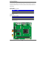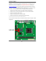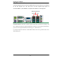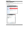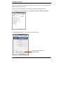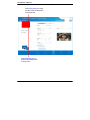
1
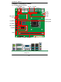
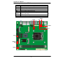
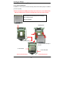
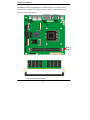
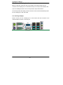
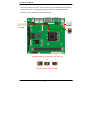
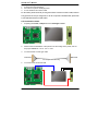
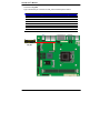
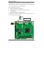
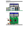
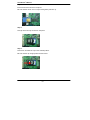
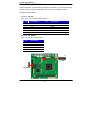
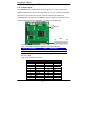
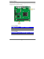
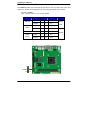
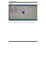
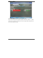
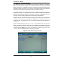
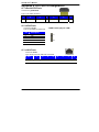
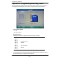
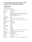
LV-67N
Mini-ITX Motherboard
User’s Manual
Edition 1.1
2015/04/30
LV-67N User’s Manual
Copyright
Copyright 2013, all rights reserved. This document is copyrighted and all rights are
reserved. The information in this document is subject to change without prior notice to
make improvements to the products.
This document contains proprietary information and protected by copyright. No part of
this document may be reproduced, copied, or translated in any form or any means
without prior written permission of the manufacturer.
All trademarks and/or registered trademarks contains in this document are property of
their respective owners.
Disclaimer
The company shall not be liable for any incidental or consequential damages resulting
from the performance or use of this product.
The company does not issue a warranty of any kind, express or implied, including
without limitation implied warranties of merchantability or fitness for a particular purpose.
The company has the right to revise the manual or include changes in the specifications
of the product described within it at any time without notice and without obligation to
notify any person of such revision or changes.
Trademark
All trademarks are the property of their respective holders.
Any questions please visit our website at http://www.commell.com.tw
TU
UT
-1-
LV-67N User’s Manual
Packing List:
Please check the package content before you starting using the board.
Hardware:
LV-67N Mini-ITX Motherborad x 1
Cable Kit:
SATA Cable x 2
(OALSATA3-L)
(1040529)
USB2.0 Cable x 1
(OALUSBA-1)
(1040172)
DVI VGA Cable x 1
(OALDVIVGA)
(1040078)
USB3.0 Cable x 1
(OALUSB3)(Option)
(1040531)
Dual COM PORT Cable x 1
(OALES-BKU2)(Option)
(1040087)
I/O Shield x 1
(OPLATE-MCDLA)
(1270055)
Printed Matters:
Driver CD (Including User’s Manual) x 1
-2-
LV-67N User’s Manual
Index
Chapter 1 <Introduction> ..............................................................................6
1.1 <Product Overview>..................................................................................... 6
1.2 <Product Specification>................................................................................ 7
1.3 <Mechanical Drawing>................................................................................. 8
1.4 <Block Diagram>.......................................................................................... 9
Chapter 2 <Hardware Setup>......................................................................10
2.1 <Connector Location> ................................................................................ 10
2.2 <Jumper Location & Reference>................................................................ 11
2.3 <Connector Reference> ............................................................................. 12
2.3.1 <Internal Connectors> ................................................................... 12
2.3.2 <External Connectors> .................................................................. 12
2.4 <CPU and Memory Setup> ........................................................................ 13
2.4.1 <CPU installation> ......................................................................... 13
2.4.2 <Memory Setup> ........................................................................... 14
2.5 <CMOS & ATX Setup> ............................................................................... 15
2.6 <Serial ATA Interface> ................................................................................ 16
2.7 <Ethernet Interface>................................................................................... 17
2.8 <Onboard Display Interface> ..................................................................... 18
2.8.1 <Analog Display>........................................................................... 18
2.8.2 <Digital Display> ............................................................................ 19
2.8.3 <VGA Interface> ............................................................................ 23
2.9 <Integrated Audio Interface> ...................................................................... 24
2.10 <USB Interface>....................................................................................... 26
2.11 <Serial Port>............................................................................................. 28
2.12 <PCIE Mini Card and SIM Interface> ....................................................... 31
2.12.1 <SIM Setup>................................................................................ 33
2.13 <GPIO and SMBUS Interface>................................................................. 35
2.14 <Power Supply and Fan Interface > ......................................................... 36
2.14.1 <Power Input> ............................................................................. 36
-3-
LV-67N User’s Manual
2.14.2 <Fan connector> ..........................................................................37
2.15 <Switch and Indicator> .............................................................................38
Chapter 3 <System Setup> .........................................................................39
3.1 <Audio Configuration> ................................................................................39
3.2 <Display Properties Setting> ......................................................................40
3.3 <SATA configuration> .................................................................................42
3.4 <SATA RAID Configuration> .......................................................................43
Chapter 4 <BIOS Setup> .............................................................................45
Appendix A <I/O Port Pin Assignment>.....................................................47
A.1 <Serial ATA Port> .......................................................................................47
A.2 <IrDA Port>.................................................................................................47
A.3 <LAN Port>.................................................................................................47
Appendix B <Flash BIOS>...........................................................................48
B.1 <Flash Tool>...............................................................................................48
B.2 <Flash BIOS Procedure> ...........................................................................48
Appendix C <Programming GPIO’s> .........................................................49
Appendix D <Programming Watchdog Timer > ........................................50
Contact Information .....................................................................................51
-4-
LV-67N User’s Manual
(This page is left for blank)
-5-
LV-67N User’s Manual
Chapter 1 <Introduction>
1.1 <Product Overview>
LV-67N the 4th Generation Intel of the Mini-ITX Motherboard , supports 4th Generation
Intel® Core™ i7, Core™ i5, Core™ i3, Celeron, Pentium Desktop Processor and
features Intel Q87 chipset, integrated HD Graphics, DDR3 memory, REALTEK High
Definition Audio, Serial ATAIII with RAID function for a system and Intel Gigabit LAN.
Intel Haswell Processor
The 4th Generation Intel® Core™ processor family desktop is the next generation of
64-bit, the processors are based on Intel® microarchitecture formerly known as Haswell,
manufactured on 22nm process technology with 3-D tri-gate transistors.
Features for Intel Q87 chipset
The board integrates Intel Q87 chipset, supports integrated HD Graphics, built-in high
speed mass storage interface of Serial ATAIII interface with RAID function, High
Definition Audio with 2 channels surrounding sound.
Flexible Extension Interface
The board provides, two mini-PCIE socket, one SIMM socket and one PCIE X16 slot.
-6-
LV-67N User’s Manual
1.2 <Product Specification>
General Specification
Form Factor
Mini-ITX motherboard
CPU
Supports 4th Generation Intel® Core™ i7/ i5/ i3/ Celeron/ Pentium Desktop
Processor.
Package type: FCLGA1150
Memory
Two DDR3/DDR3L (support 1.5V) 1333/1600 LO-DIMM up to 16GB
Chipset
Intel Q87 Express chipset
Real Time Clock
Chipset integrated RTC with onboard lithium battery
Watchdog Timer
Generates a system reset with internal timer for 1min/s ~255min/s
Power Management
Supports ACPI 4.0 compliant
Serial ATA Interface
Intel® Q87 PCH built-in 4 x Serial ATAIII interface up to 600MB/s Support
Support Non-ECC, unbuffered memory only
RAID 0, 1, 5, 10 and Intel Rapid Storage Technology.
(not support SATA II device)
VGA Interface
Intel® Clear Video integrated HD Graphics Technology
DVI Interface
Onboard DVI connector
LVDS Interface
Onboard 24-bit dual channel LVDS connector with +3.3V/+5V/+12V supply
Display port Interface Onboard Display port connector
Audio Interface
Intel® integrated Q87 with Realtek ALC888 HD Audio.
LAN Interface
1 x Intel® I210 Gigabit LAN
1 x Intel® I217-LM Gigabit LAN
GPIO interface
Onboard programmable 8-bit Digital I/O interface
Extended Interface
One PCIE X 16 slot, Two PCIE Mini card, One SIM socket
(Optional support mSATA(SATAIII) for Mini_Card1)
Internal I/O Port
2 x RS232, 1 x GPIO port, 1 x Audio connector, 1 x IrDA connector, 1 x
SMBUS connector, 1 x CRT, 1 x LVDS, 1 x LPC, 4 x USB2.0 and 2 x USB3.0
ports, 4 x SATAIII
External I/O Port
1 x PS/2 Keyboard/Mouse Port, 1 x RS232, 1 x RS232/422/485, 1 x DVI port,
1 x Display port, 2 x RJ45 LAN ports and 4 x USB3.0 ports.
Power Requirement
Standard ATX 24-pin (20-pin is compatible) power supply and P4 4-pin 12V
Dimension
170mm x 170mm
Temperature
Operating within 0~60 centigrade
Storage within –20~85 centigrade
Ordering Code
LV-67N
Onboard DVI, Display Port, CRT, LVDS, 2 x Gigabit LAN, USB3.0 & 2.0,
Serial Port, SATAIII, IrDA, Realtek HD Audio, PCIE Mini card, PCIE x16,
SMBUS, GPIO, SIM, LPC, mSATA
The specifications may be different as the actual production.
For further product information please visit the website at http://www.commell.com.tw
TU
-7 -
UT
LV-67N User’s Manual
1.3 <Mechanical Drawing>
-8 -
LV-67N User’s Manual
1.4 <Block Diagram>
1 x PCI Express x16
4th Generation Intel® Core™ i7,
Core™ i5, Core™ i3, Celeron,
Pentium Processor
2 x 240-pin DDR3
LO-DIMM
1333/1600 MHz
up to 16GB
1 x DVI
1 x Display port
1 x LVDS
1 x CRT
2 x PCI Express mini card
Q87
6 x USB 3.0
4 x USB 2.0
4 x Serial ATAIII
1 x Intel I210
ALC888 HD Audio
1 x Intel I217-LM
W25Q128 SPI
1 x RS232/422/485
W83627DHG-P
1 x RS232 & GPIO & IrDA
& LPC
1 x PS/2
F81216
-9 -
2 x RS232
LV-67N User’s Manual
Chapter 2 <Hardware Setup>
2.1 <Connector Location>
CN_AUDIO
CN_LPC CN_COM3/4
CN_CRT
CN_LVDS
CN_INV
CPUFAN
CN_12V
MINI_CARD1
CN_DIO
CN_IR
S_ATA3/S_ATA4
CN_SMBUS
S_ATA1/S_ATA2
CN_USB1/2
MINI_CARD2
CN_SIMM
JFRNT
CN_USB3
PS2
COM1+COM2
SYSFAN
DDRIII_A/B
ATX
USB_RJ45_1/2
DVI
Display Port
-10-
Audio
LV-67N User’s Manual
2.2 <Jumper Location & Reference>
Jumper
JRTC
JVLCD
JAT
JP1
JP2
JCSEL1
JCSEL2
JVUSB
JMSATA
Function
CMOS Operating/Clear Setting
Panel Voltage Setting
Power mode select
Com1 Voltage Setting (For Pin 9)
Com2 Voltage Setting (For Pin 9)
COM2 RS-232 RS422 RS485 Setting
CN_IR IrDA Setting
USB Voltage Setting
Mini Card1 mSATA Setting
JVLCD
JCSEL1
JP1
JCSEL2
JP2
JRTC
JMSATA
JAT
JVUSB
-11-
LV-67N User’s Manual
2.3 <Connector Reference>
2.3.1 <Internal Connectors>
Connector
CPU
DDRIII A/B
S_ATA 1/2/3/4
DC_12V
ATX
CN_AUDIO
CDIN
CN_DIO
CN_USB 1/2
CN_USB3
CPUFAN
SYSFAN
CN_CRT
CN_LVDS
CN_INV
CN_IR
CN_COM 3/4
CN_LPC
JFRNT
PCIE
Mini-PCIE1/2
SIMM
JAT
JSPD 1/2
JACT 1/2
Function
LGA1150 CPU Socket
240-pin DDR3 LO-DIMM socket
7-pin Serial ATAIII connector
4-pin +12V additional power supply connector
24-pin power supply connector
5 x 2-pin audio connector
4-pin CD-ROM audio input connector
6 x 2-pin digital I/O connector
10-pin USB connector
20-pin USB3.0 connector
4-pin CPU cooler fan connector
3-pin system cooler fan connector
16-pin VGA connector
20 x 2-pin LVDS connector
5-pin LCD inverter connector
5-pin IrDA connector
9-pin RS232
5 x 2-pin LPC connector
14-pin front panel switch/indicator connector
164-pin x16 PCIE slot
2 x 52-pin Mini-PCIE socket
6-pin socket
Power mode select
LAN Speed LED connector
LAN Activity LED connector
Remark
2.3.2 <External Connectors>
Connector
USB_RJ45 1/2
DVI + Display port
COM 1/2
PS/2
AUDIO
Function
2 x USB3.0 and 1 x RJ45 LAN connector
DVI connect and Display port connector
Serial port connector
PS/2 keyboard and mouse connector
Audio connector
-12-
Remark
LV-67N User’s Manual
2.4 <CPU and Memory Setup>
2.4.1 <CPU installation>
LV-67N has a LGA1150 CPU socket onboard; please check following steps to install the
processor properly.
Attention If LV-67N need RMA please Keep CPU socket cover on the CPU Socket.
Warning If CPU Socket internal Pin damage We could not provide warranty.
Intel® I3/I5/I7/Celeron/Pentium processor Package
type: 1150 pin FCLGA
FSB:1333/1600MHz
1. Lift this bar
Checked point
2. Uncover this plate
3. Place the CPU on the top of
the pins
4. Lock this bar
5. Cover this plate
Notice: Please place the CPU on the pins tenderly to avoid bending the pins
-13-
LV-67N User’s Manual
2.4.2 <Memory Setup>
LV-67N has two 240-pin DDR3/DDR3L LO-DIMM support up to 16GB of memory
capacity and 1.5 Voltage. The memory frequency supports 1333/1600 MHz. Only
Non-ECC memory is supported.
DDRIII_A
DDRIII_B
Please check the pin number to match the socket side well
before installing memory module.
-14-
LV-67N User’s Manual
2.5 <CMOS & ATX Setup>
The board’s data of CMOS can be setting in BIOS. If the board refuses to boot due to
inappropriate CMOS settings, here is how to proceed to clear (reset) the CMOS to its
default values.
Jumper: JRTC
Type: Onboard 3-pin jumper
JRTC
Mode
1-2
Clear CMOS
2-3
Normal Operation
Default setting: 2-3
Jumper: JAT
Type: onboard 3-pin jumper
JAT
Mode
1-2
AT Mode
2-3
ATX Mode
Default setting:2-3
1
3
JRTC
1
3
JAT
-15-
LV-67N User’s Manual
2.6 <Serial ATA Interface>
LV-67N has Four Serial ATA III interfaces with RAID function, the transfer rate of the
Serial ATA III can be up to 600MB/s, but not supports SATAII device. Please go to
http://www.serialata.org/ for more about Serial ATA technology information. Based on
Intel® PCH, it supports Intel® Matrix Storage Technology with combination of RAID
0,1,5 and 10. The main features of RAID on Intel® Q87 PCH are listed below:
1.
Supports for up to RAID volumes on a single, two-hard drive RAID array.
2.
Supports for two, two-hard drive RAID arrays on any of six Serial ATA ports.
3.
Supports for Serial ATA ATAPI devices.
4.
Supports for RAID spares and automatic rebuild.
5.
Supports on RAID arrays, including NCQ and native hot plug.
For more information please visit Intel’s official website.
For more about the system setup for Serial ATA, please check the chapter of SATA
configuration.
S_ATA3 / S_ATA4
S_ATA1 / S_ATA2
-16-
LV-67N User’s Manual
2.7 <Ethernet Interface>
The board integrates with one Intel I210 Gigabit Ethernet & one Intel I217-LM controllers,
as the PCI Express bus. The Intel I210 & I217-LM supports triple speed of
10/100/1000Base-T, with IEEE802.3 compliance and Wake-On-LAN supported.
RJ45 LAN connector
I217-LM
I210
Onboard Intel® I217-LM GbE controller support Intel® AMT 9.0 feature on primary LAN
port. The BIOS is ready to support Intel® AMT 9.0 feature. The necessary prerequisite is
your CPU must support Intel® vPro technology, ex : Intel® Core™ i7
For further instruction about the Intel® AMT features and set up, please refer to the
iAMT Setting.pdf.
-17-
LV-67N User’s Manual
2.8 <Onboard Display Interface>
Based on Intel Q87 chipset with built-in HD Graphic, the board provides one DVI
connector & one Display port on real external I/O port, one 40-pin LVDS interface with
5-pin LCD backlight inverter connector and provides 16-pin VGA interface.
The board provides dual display function with clone mode and extended desktop mode
for DVI, Display port, VGA and LVDS.
2.8.1 <Analog Display>
Please connect your DVI & Display port or LCD monitor with male connector to the
onboard female connector on rear I/O port .
DVI
Display port
-18-
LV-67N User’s Manual
2.8.2 <Digital Display>
The board provides one 40-pin LVDS connector for 24-bit single/dual channel panels,
supports up to 2048 x 1536 (UXGA) resolution, with one LCD backlight inverter
connector and one jumper for panel voltage setting.
1
1
39
40
2
CN_LVDS
5
CN_INV
1
2
5
6
JVLCD
Effective patterns of connection: 1-2 / 3-4 / 5-6
5
3
1
6
4
2
Warning: others cause damages
-19-
LV-67N User’s Manual
Connector: CN_INV
Type: 5-pin LVDS Power Header
Connector: JVLCD
Type: 6-pin Power select Header
Pin
Description
1
+12V
2
Reserved (Note)
3
GND
4
GND
5
ENABKL
Note: Reserved for MB internal test
Please treat it as NC.
Pin
Description
1-2
LCDVCC (3.3V)
3-4
LCDVCC (5V)
5-6
LCDVCC (12V)
Default: 1-2
Connector: CN_LVDS
Type: onboard 40-pin connector for LVDS connector
Connector model: HIROSE DF13-40DP-1.25V or compatible
Pin
2
4
6
8
10
12
14
16
18
20
22
24
26
28
30
32
34
36
38
40
Signal
LCDVCC
GND
ATX0ATX0+
GND
ATX1ATX1+
GND
ATX2ATX2+
GND
ACLKACLK+
GND
ATX3ATX3+
GND
DDCPCLK
DDCPDATA
N/C
-20-
Pin
1
3
5
7
9
11
13
15
17
19
21
23
25
27
29
31
33
35
37
39
Signal
LCDVCC
GND
BTX0BTX0+
GND
BTX1BTX1+
GND
BTX2BTX2+
GND
BTX3BTX3+
GND
BCLKBCLK+
GND
SMBCKL
SMBDATA
SPDIFO
LV-67N User’s Manual
To setup the LCD, you need the component below:
1. A panel with LVDS interfaces.
2. An inverter for panel’s backlight power.
3. A LCD cable and an inverter cable.
For the cables, please follow the pin assignment of the connector to make a cable, because
every panel has its own pin assignment, so we do not provide a standard cable; please find
a local cable manufacture to make cables.
LCD Installation Guide:
1.
Preparing the LV-67N, LCD panel and the backlight inverter.
2.
Please check the datasheet of the panel to see the voltage of the panel, and set
the jumper JVLCD to +12V or +5V or +3.3V.
3.
You would need a LVDS type cable.
Panel side
Board side
For sample illustrator only
4.
To connect all of the devices well.
-21-
LV-67N User’s Manual
After setup the devices well, you need to select the LCD panel type in the BIOS.
The panel type mapping is list below:
BIOS panel type selection form (BIOS Version:1.0)
Single / Dual channel
Single / Dual channel
NO.
Output format
NO.
1
640 x 480
9
1680 x 1050
2
800 x 600
10
1920 x 1200
3
1024 x 768
11
1440 x 900
4
1280 x 1024
12
1600 x 900
5
1400 x 1050 Reduced Blanking
13
1024 x 768
6
1400 x 1050 non-Reduced Blanking
14
1280 x 800
7
1600 x 1200
15
1920 x 1080
8
1366 x 768
16
2048 x 1536
-22-
Output format
LV-67N User’s Manual
2.8.3 <VGA Interface>
Connector: CN_CRT
Type: onboard 16-pin connector for CN_VGA connector pitch 2.00mm
Pin
1
3
5
7
9
11
13
15
2
Signal
BR
BB
-CRTATCH
IOGND1
NC
NC
5HSYNC
5VCLK
Pin
2
4
6
8
10
12
14
16
16
1
15
CN_CRT
-23-
Signal
BG
NC
IOGND1
IOGND1
-CRTATCH
5VCDA
5VSYNC
NC
LV-67N User’s Manual
2.9 <Integrated Audio Interface>
The board integrates onboard audio interface with REALTEK ALC888 code, with Intel
next generation of audio standard as High Definition Audio, it offers more vivid sound
and other advantages than former HD audio compliance.
The main specifications of ALC888 are:
z
High-performance DACs with 100dB S/N ratio
z
2 DAC channels support 16/20/24-bit PCM format for 2 audio solution
z
Compatible with HD
z
Meets Microsoft WHQL/WLP 2.0 audio requirements
The board provides 2 channels audio phone jacks on rear I/O port, Line-in/MIC-in ports
for front I/O panel through optional cable.
LINE-IN
LINE-OUT
MIC-IN
2
10
1
9
CN_AUDIO
-24-
Rear I/O phone jacks
LV-67N User’s Manual
Connector: CN_AUDIO
Type: 10-pin (2 x 5) header (pitch = 2.54mm)
Pin
1
3
5
7
9
Description
MIC_L
MIC_R
Speaker_R
SENSE
Speaker_L
Pin
2
4
6
8
10
-25-
2
10
1
9
Description
Ground
N/C
MIC Detect
N/C
Speaker Detect
LV-67N User’s Manual
2.10 <USB Interface>
LV-67N integrates six USB3.0 ports and four USB2.0 ports.
The specifications of USB3.0 are listed below:
Interface
USB3.0
Controller
Intel® Q87
Transfer Rate
Up to 5Gb/s
Voltage
5V
USB1/2/3/4
Type: USB3.0
The specifications of USB2.0 are list:
Interface
USB2.0
Controller
Intel®Q87
Transfer Rate
Up to 480Mb/s
Voltage
5V
CN_USB1/2
Type: USB2.0
1
2
9
10
1
2
5
6
JVUSB
-26-
LV-67N User’s Manual
Connector: CN_USB3
Type: 20-pin (2 x 10) header (pitch = 2.0mm)
Pin
1
2
3
4
5
6
7
8
9
10
Description
VCC (5V_SB/ 5V)
USB3.0_RX0USB3.0_RX0+
Ground
USB3.0_TX0USB3.0_TX0+
Ground
Data0Data0+
NC
Pin
20
19
18
17
16
15
14
13
12
11
Description
NC
VCC (5V_SB/ 5V)
USB3.0_RX1USB3.0_RX1+
Ground
USB3.0_TX1USB3.0_TX1+
Ground
Data1Data1+
Connector: CN_USB1/2
Type: 10-pin (2 x 5) header (pitch = 2.54mm)
Pin
1
3
5
7
9
Description
VCC (5V_SB/ 5V)
Data0Data0+
Ground
Ground
Pin
2
4
6
8
10
Description
VCC (5V_SB/ 5V)
Data1Data1+
Ground
N/C
Connector: JVUSB
Type: 6-pin Power select jumper
Pin
1-3 & 2-4
3-5 & 4-6
Default: 1-3 & 2-4
Description
5V_SB
5V
Effective patterns of connection: 1-3 & 2-4 or 3-5 & 4-6
1
2
1
2
5
6
5
6
Warning: others cause damages
-27-
LV-67N User’s Manual
2.11 <Serial Port>
The board supports Three RS232 serial port and one jumper selectable
RS232/422/485 serial ports. The jumper JCSEL1 & JCSEL2 can let you configure
the communicating modes for COM2.
COM2
COM1
Connector: COM1
Type: 9-pin D-sub male connector on bracket for COM1
Pin
1
3
5
7
9
Description
DCD
TXD
GND
RTS
RI
Pin
2
4
6
8
10
Description
RXD
DTR
DSR
CTS
N/C
Connector: COM2
Type: 9-pin D-sub male connector on bracket for COM2
Pin
1
3
5
7
9
Description
DCD/422TX-/485TXD/422RX+
GND
RTS
RI
Pin
2
4
6
8
10
Setting RS-232 & RS-422 & RS-485 for COM2
-28-
Description
RXD/422TX+/485+
DTR/422RXDSR
CTS
N/C
LV-67N User’s Manual
Connector: COM3/4
Type: 20-pin (2 x 10) header pitch = 2.54x1.27mm
Pin
1
3
5
7
9
11
13
15
17
19
Description
DCD1
TXD1
GND1
RTS1
RI1
DCD2
TX2
Ground
RTS2
RI2
Pin
2
4
6
8
10
12
14
16
18
20
COM3/4
2
20
1
19
Description
RXD1
DTR1
DSR1
CTS1
N/C
RX2
DTR2
DSR2
CTS2
N/C
2
JP1
6
2
1
5
1
12
JCSEL1
11
JCSEL2
2
8
1
7
2
6
1
5
JP2
-29-
LV-67N User’s Manual
Function
JCSEL2
JCSEL1
2
12
2
8
1
7
2
8
2
12
1
7
1
11
2
8
2
12
1
7
1
11
2
8
2
12
1
7
1
11
IrDA
1
11
RS-422
RS-485
RS-232
Default setting:
JCSEL1: (1-3, 2-4, 7-9, 8-10) JCSEL2: (1-2)
Jumper: JP1/JP2 (COM1/2)
Type: onboard 6-pin header
Power Mode
JP1/2
Pin 9 with 5V Power
1-2
Pin 9 with 12V Power
3-4
Standard COM port
5-6
Default setting
-32-
LV-67N User’s Manual
2.12 <PCIE Mini Card and SIM Interface>
The board provides two PCIE mini card sockets and a SIM socket.
MINI_CARD1 is the first Mini-PCIe slot for long size Mini-PCIe cards.
MINI_CARD1 slot and option support mSATA.
MINI_CARD2 is the second Mini-PCIe slot for long size Mini-PCIe cards.
However, if you are trying to use 3G Mini-PCIe card with a SIM card then place your 3G
Mini-PCIe card in this slot and put your SIM card into the SIM card socket beneath this
MINI_CARD2 support 3G PCIE Mini card with SIM.
MINI_CARD1
7
6
5
3
2
1
MINI_CARD2
1
JMSATA
3
Connector: SIMM
Type: 6-pin SIM socket
Pin
1
3
5
7
Description
SIMVCC
SIMCLK
GND
SIMDATA
Pin
2
4
6
-31-
Description
SIMRST
NC
SIMVPP
LV-67N User’s Manual
Jumper: JMSATA
Type: onboard 3-pin header
MINI_CARD Mode
JMPCIE
Supply mSATA(only support SATAIII)
1-2
MINI_CARD
2-3
Default setting:
2-3
-32-
LV-67N User’s Manual
2.12.1 <SIM Setup>
Step1.
SIM card holder is marked by circle.
Slide the cap toward OPEN direction.
Step 2.
Make sure that the cap is now at the OPEN position.
Step 3.
Flip the cap up for inserting a SIM card into.
-33-
LV-67N User’s Manual
Step 4.
Insert a SIM card as shown in the photo.
Be sure that the corner cut is on top and the golden pads are up.
Step 5.
Now, flip down the cap as shown in the photo.
Step 6.
Press down and slide the cap to the CLOSE position.
Be sure that the cap is tightly held with the socket.
-34-
LV-67N User’s Manual
2.13 <GPIO and SMBUS Interface>
The board provides a programmable 8-bit digital I/O interface; you can use this general
purpose I/O port for system control like POS or KIOSK, and a SMBUS (System
Management Bus) interface.
Connector: CN_DIO
Type: 12-pin (6 x 2) header (pitch = 2.0mm)
Pin
1
3
5
7
9
11
Description
Ground
GP10
GP11
GP12
GP13
5V
Pin
2
4
6
8
10
12
Description
Ground
GP14
GP15
GP16
GP17
12V
Connector: CN_SMBUS
Type: 5-pin header for SMBUS Ports
Pin
1
2
3
4
5
Description
VCC
N/C
SMBDATA
SMBCLK
Ground
2
1
12
11
CN_DIO
1
5
CN_SMBUS
-35-
LV-67N User’s Manual
2.14 <Power Supply and Fan Interface >
2.14.1 <Power Input>
The LV-67N provides a standard ATX power supply with 24-pin ATX connector and
additional 12V connector, and the board provides one 4-pin fan connectors supporting
smart fan for CPU cooler and one 3-pin cooler fan connectors for system and
Northbridge chip. The 4-pin CN_12V additional power connector is necessary for CPU
powering; please connect this well before you finishing the system setup.
3
4
CN_12V
1
2
13
ATX
1
Connector: CN_12V
Type: 4-pin standard Pentium 4 additional +12V power connector
Pin
Description
Pin
Description
1
Ground
2
Ground
3
+12V
4
+12V
Connector: ATX
Type: 24-pin ATX power connector
PIN assignment
1
3.3V
2
3.3V
3
GND
4
5V
5
GND
6
5V
7
GND
8
PW_OK
9
5V_SB
10
12V
11
12V
12
3.3V
13
14
15
16
17
18
19
20
21
22
23
24
-36-
3.3V
-12V
GND
-PSON
GND
GND
GND
N/C
5V
5V
5V
GND
24
12
LV-67N User’s Manual
2.14.2 <Fan connector>
The board provides one 4-pin fan connectors supporting smart fan for CPU cooler and
one 3-pin cooler fan connectors for system.
CPUFAN
1
4
1
3
SYSFAN
Connector: CPUFAN
Type: 4-pin fan wafer connector
Pin
Description
1
Ground
3
Fan Speed Detection
Connector: SYSFAN
Type: 3-pin fan wafer connector
Pin Description
Pin
1
Ground
2
Pin
2
4
Description
+12V
Fan Control
Description
+12V
-37-
Pin
3
Description
Sense
LV-67N User’s Manual
2.15 <Switch and Indicator>
The JFRNT provides front control panel of the board, such as power button, reset and
beeper, etc. Please check well before you connecting the cables on the chassis.
Connector: JFRNT
Type: onboard 14-pin (2 x 7) 2.54-pitch header
Function
Signal
PIN
Signal
HDLED+
1
2
PWRLED+
HDLED-
3
4
N/C
Reset+
5
6
PWRLED-
Reset-
7
8
SPK+
N/C
9
10
N/C
Power
PWRBT+
11
12
N/C
Button
PWRBT-
13
14
SPK-
IDE LED
Function
Power
LED
Reset
Speaker
1
2
JFRNT
13
14
-38-
LV-67N User’s Manual
Chapter 3 <System Setup>
3.1 <Audio Configuration>
The board integrates Intel® Q87 with REALTEK® ALC888 code. It can support
2-channel sound under system configuration. Please follow the steps below to setup
your sound system.
1.
Install REALTEK HD Audio driver.
2.
Lunch the control panel and Sound Effect Manager.
3.
Select Speaker Configuration
-39-
LV-67N User’s Manual
3.2 <Display Properties Setting>
Based on Intel Q87 with HD Graphic, the board supports two DACs for display device as
different resolution and color bit.
Please install the Intel Graphic Driver before you starting setup display devices.
1. Click right button on the desktop to lunch Screen resolution > Advanced settings
2. Click Graphics Properties… button for more specificity setup.
Click Graphics Properties... for
advanced setup
-40-
LV-67N User’s Manual
3. This setup options can let you define each device settings.
Click Display Settings to setup
the CRT monitor for Resolution
and Refresh Rate
Click Multiple Displays to
setup the dual display mode
as same screen
-41-
LV-67N User’s Manual
3.3 <SATA configuration>
SATA Mode:
This option can let you select whether the Serial ATA hard drives would work under normal
IDE or AHCI or RAID mode. The RAID mode need more than one HDD is applied.
-42-
LV-67N User’s Manual
3.4 <SATA RAID Configuration>
The board integrates Intel® Q87 PCH with RAID function for Serial ATA drives, and
supports the configurations below:
RAID 0 (Stripping): Two hard drives operating as one drive for optimized data R/W
performance. It needs two unused drives to build this operation.
RAID 1 (Mirroring): Copies the data from first drive to second drive for data security,
and if one drive fails, the system would access the applications to the workable drive. It
needs two unused drives or one used and one unused drive to build this operation. The
second drive must be the same or lager size than first one.
RAID 5 (striping with parity)
A RAID 5 array contains three or more hard drives where the data is divided into
manageable blocks called strips. Parity is a mathematical method for recreating data
that was lost from a single drive, which increases fault-tolerance. The data and parity
are striped across all the hard drives in the array. The parity is striped in a rotating
sequence to reduce bottlenecks associated with the parity calculations.
RAID 10 (RAID 0+1)
A RAID 10 array uses four hard drives to create a combination of RAID levels 0 and 1.
The data is striped across a two-drive array forming the RAID 0 component. Each of the
drives in the RAID 0 array is then mirrored by a RAID 1 component.
Intel Matrix Storage Technology: This technology would allow you to use RAID 0+1
mode on only two drives (4 drives needed on traditional RAID 0+1). It will create two
partitions on each hard drive to simulate RAID 0 and RAID 1. It also can let you modify
the partition size without re-formatted.
For more information of Intel Matrix Storage Technology, please visit Intel’s website.
If you need to install an operation system on the RAID set, please use the driver disk
attached in the package when it informs you to obtain the RAID drivers.
-43-
LV-67N User’s Manual
Please press <CTRL+I> to enter the RAID configuration menu.
You can setup the RAID under operation system for Microsoft® Windows 7 , please
install the Intel® Application Accelerator Ver.4.5 later to support RAID configuration with
Intel® Matrix Storage Technology.
-44-
LV-67N User’s Manual
Chapter 4 <BIOS Setup>
The motherboard uses the Phoenix BIOS for the system configuration. The Phoenix
BIOS in the single board computer is a customized version of the industrial standard
BIOS for IBM PC AT-compatible computers. It supports Intel x86 and compatible CPU
architecture based processors and computers. The BIOS provides critical low-level
support for the system central processing, memory and I/O sub-systems.
The BIOS setup program of the single board computer let the customers modify the basic
configuration setting. The settings are stored in a dedicated battery-backed memory,
NVRAM, retains the information when the power is turned off. If the battery runs out of
the power, then the settings of BIOS will come back to the default setting.
The BIOS section of the manual is subject to change without notice and is provided here
for reference purpose only. The settings and configurations of the BIOS are current at
the time of print, and therefore they may not be exactly the same as that displayed on
your screen.
To activate CMOS Setup program, press <DEL> key immediately after you turn on the
system. The following message “Press DEL to enter SETUP” should appear in the lower
left hand corner of your screen. When you enter the CMOS Setup Utility, the Main Menu
will be displayed as Figure 4-1. You can use arrow keys to select your function, press
<Enter> key to accept the selection and enter the sub-menu.
Figure 4-1 CMOS Setup Utility Main Screen
-45-
LV-67N User’s Manual
(This page is left for blank)
-46-
LV-67N User’s Manual
Appendix A <I/O Port Pin Assignment>
A.1 <Serial ATA Port>
Connector: S_ATA1/2/3/4
Type: 7-pin wafer connector
1
2
7
3
4
1
5
6
7
GND RSATA_TXP1 RSATA_TXN1 GND RSATA_RXN1 RSATA_RXP1 GND
A.2 <IrDA Port>
Connector: CN_IR
Type: 5-pin header for SIR Ports
Pin
1
2
3
4
5
JCSEL1 must jump to “SIR”
Description
VCC
N/C
IRRX
Ground
IRTX
1
5
A.3 <LAN Port>
Connector: RJ45
Type: RJ45 connector with LED on bracket
Pin
Description
1
2
3
4
MI0+
MI0-
MI1+
MI2+
-47-
8
5
6
MI2- MI1-
1
7
8
MI3+
MI3-
LV-67N User’s Manual
Appendix B <Flash BIOS>
B.1 <Flash Tool>
The board is based on Phoenix BIOS and can be updated easily by the BIOS auto
flash tool. You can download the tool online at the address below:
http://www.phoenix.com/en/home/
http://www.commell.com.tw/Support/Support_SBC.htm
File name of the tool is “Fpt.exe”, it’s the utility that can write the data into the BIOS
flash ship and update the BIOS.
B.2 <Flash BIOS Procedure>
1. Please make a bootable floppy disk.
2. Get the last .bin files you want to update and copy it into the disk.
3. Copy Fpt.exe to the disk.
4. Power on the system and flash the BIOS.
(Example: C:/Fpt –savemac –f XXX.bin )
5. Restart the system.
Any question about the BIOS re-flash please contact your distributors or visit the
web-site at below:
http://www.commell.com.tw/support/support.htm
UT
-48-
LV-67N User’s Manual
Appendix C <Programming GPIO’s>
The GPIO’can be programmed with the MSDOS debug program using
simple IN/OUT commands.The following lines show an example how to
do this.
GPIO0…..GPIO7 bit0……bit7
-o 2 E 87
;enter configuration
-o 2E 87
-o 2E 07
-o 2F 09
;enale GPIO function
-o 2E 30
-o 2F 02
;enable GPIO configuration
-o 2E F0
-o 2F xx
;set GPIO as input/output; set ‘1’ for input,’0’for
output
-o 2E F1
-o 2F xx
;if set GPIO’s as output,in this register its value can
be set
Optional :
-o 2E F2
-o 2F xx
; Data inversion register ; ‘1’ inverts the current valus
of the bits ,’0’ leaves them as they are
-o 2E 30
-o 2F 01
; active GPIO’s
For further information, please refer to Winbond W83627DHG-P datasheet.
-49-
LV-67N User’s Manual
Appendix D <Programming Watchdog Timer >
The watchdog timer makes the system auto-reset while it stops to work for a period.
The integrated watchdog timer can be setup as system reset mode by program.
Timeout Value Range
- 1 to 255
- Second or Minute
Program Sample
Watchdog timer setup as system reset with 5 second of timeout
2E, 87
2E, 87
2E, 07
2F, 08
Logical Device 8
2E, 30
Activate
2F, 01
2E, F5
Set as Second*
2F, 00
2E, F6
Set as 5
2F, 05
* Minute: bit 3 = 1; Second: bit 3 = 0
You can select Timer setting in the BIOS, after setting the time options, the system
will reset according to the period of your selection.
-50-
LV-67N User’s Manual
Contact Information
Any advice or comment about our products and service, or
anything we can help you please don’t hesitate to contact with us.
We will do our best to support you for your products, projects and
business.
Taiwan Commate Computer Inc.
19F., No.94, Sec. 1, Xintai 5th Rd., Xizhi Dist., New Taipei
Address
City 22102, Taiwan
TEL
+886-2-26963909
FAX
+886-2-26963911
http://www.commell.com.tw
Website
TU
UT
[email protected] (General Information)
TU
UT
E-Mail
[email protected] (Technical Support)
TU
Facebook
Twitter
UT
https://www.facebook.com/pages/Taiwan-Commate-Computer-Inc/547993955271899
https://twitter.com/Taiwan_Commate
Commell is a brand name of Taiwan commate computer Inc.
-51-