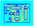
1
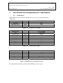
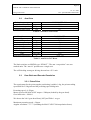
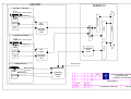
E U R O P E A N S O U T H E R N O B S E R V A T ORY
Organisation Européenne pour des Recherches Astronomiques dans l'Hémisphère Austral
Europäische Organisation für astronomische Forschung in der südlichen Hemisphäre
LA SILLA OBSERVATORY
FEROS ADC CONTROL ELECTRONICS
Doc. No.: 2p2-DSD-ESO-60400-0001
Issue: 2.0
Date: 10 – January - 2005
Prepared: J. Alonso
Name
Date
Signature
Date
Signature
Approved: G. Andreoni
Name
Released: G. Andreoni
Name
Date
Signature
Page 2
FEROS ADC CONTROL ELECTRONICS
10- 01 - 2005
Doc. 2p2-DSD-ESO-60400-0001
Design Document
CHANGE RECORD
Revision
Date
Section/Paragraph
Remarks
Issue 1.0
Issue 2.0
18/04/2004
10/01/2005
All
Section 3
Section 4
Section 6
Section 6
Section 5.5
First Issue
Tables updated.
Tables corrected after testing of the hardware.
Several schematic diagrams corrected.
PCBs drawings added.
VME4SA-I components settings added.
Page 3
FEROS ADC CONTROL ELECTRONICS
10- 01 - 2005
Doc. 2p2-DSD-ESO-60400-0001
Design Document
INDEX OF CONTENTS
1.
INTRODUCTION .............................................................................................................................5
1.1.
1.2.
1.3.
1.4.
2.
ADC MOTION CONTROL .............................................................................................................8
2.1.
2.2.
2.3.
2.4.
2.5.
3.
PURPOSE AND SCOPE.............................................................................................................5
REFERENCE DOCUMENTS.....................................................................................................5
APPLICABLE DOCUMENTS ...................................................................................................5
ACRONYMS & ABBREVIATIONS..........................................................................................7
MOTION CONTROL CONCEPT........................................................................................................8
MOTION CONTROL COMPONENTS.................................................................................................8
MOTION CONTROL FUNCTIONS ....................................................................................................8
PRISM POSITION AND SPEED CONTROL LOOP ................................................................................9
ARM POSITION TORQUE CONTROL .............................................................................................10
ADC DRIVES ELECTROMECHANICAL COMPONENTS ....................................................11
3.1. PRISM DRIVE ..............................................................................................................................11
3.2. ARM DRIVE ................................................................................................................................12
3.3. GEAR RATIO AND ENCODER RESOLUTION ..................................................................................12
3.3.1.
Prism Drive .......................................................................................................................12
3.3.2.
Arm Drive..........................................................................................................................13
4.
FEROS LCU ACROMAG DIGITAL I/O.....................................................................................13
4.1.
4.2.
4.3.
4.4.
5.
ADC CABLING...............................................................................................................................18
5.1.
5.2.
5.3.
5.4.
5.5.
6.
SCSM AND ARM INTERLOCK REPORTING .................................................................................14
ARM STATUS ..............................................................................................................................14
ARM COMMAND .........................................................................................................................15
P2 PIN-OUT AND BIT ASSIGNMENT .............................................................................................15
ADC...........................................................................................................................................18
ADC TO ADAPTER CONNECTOR PANEL ......................................................................................18
ADAPTER CONNECTOR PANEL TO LCU.......................................................................................18
INSIDE THE LCU.........................................................................................................................18
VME4SA-I COMPONENT ADAPTER CONFIGURATION ................................................................19
DRAWING AND SCHEMATIC DIAGRAM APPENDIX .........................................................20
6.1.
6.2.
6.3.
6.4.
6.5.
6.6.
6.7.
6.8.
6.9.
6.10.
6.11.
6.12.
6.13.
6.14.
BLOCK DIAGRAM .......................................................................................................................20
ARM TORQUE DRIVE LCU LAYOUT ..........................................................................................20
PRISM SERVO CABLE (LCU TO ADAPTER) .................................................................................20
ARM CABLE (LCU TO ADAPTER)..............................................................................................20
PRISM DRIVE CONNECTION BLOCK ............................................................................................20
PRISM DRIVE LINE DRIVERS SCHEMATIC ...................................................................................20
ARM CONNECTION BLOCK .........................................................................................................20
ARM-SCSM INTERLOCK SCHEMATIC .......................................................................................20
ARM TORQUE DRIVE CONNECTION BLOCK ................................................................................20
ARM TORQUE DRIVE MODULE SCHEMATIC 1.........................................................................20
ARM TORQUE DRIVE MODULE SCHEMATIC 2.........................................................................20
FEROS ADC PRISM DRIVE CONNECTION PCB .......................................................................20
FEROS ADC ARM INTERLOCK PCB ......................................................................................20
FEROS/WFI MIRROR SELECTOR AND ADC ARM CIRCUIT PCB..............................................20
Page 4
FEROS ADC CONTROL ELECTRONICS
10- 01 - 2005
Doc. 2p2-DSD-ESO-60400-0001
Design Document
INDEX OF FIGURES AND TABLES
FIGURE 1: ADC CONTROL ELECTRONICS BLOCK DIAGRAM ........................................................................9
TABLE 1: PRISM DRIVE GEAR HEAD ..........................................................................................................11
TABLE 2: PRISM DRIVE DC MOTOR ...........................................................................................................11
TABLE 3: PRISM DRIVE INCREMENTAL ENCODER ......................................................................................11
TABLE 4: ARM DRIVE GEAR HEAD ............................................................................................................12
TABLE 5: ARM DRIVE DC MOTOR .............................................................................................................12
TABLE 6: ADC ARM AND SCSM STATES STATUS REPORTING ..................................................................14
TABLE 7: ADC ARM STATES STATUS REPORTING .....................................................................................14
TABLE 8: ADC ARM CONTROL ..................................................................................................................15
TABLE 9 : ACRO DIGITAL I/O PIN-OUT AND BIT ASSIGNMENT....................................................................17
TABLE 10 : ADAPTER INTERNAL CABLING ..................................................................................................18
TABLE 11 : VME4SA COMPONENT ADAPTER CONFIGURATION ................................................................19
Page 5
FEROS ADC CONTROL ELECTRONICS
Design Document
1.
10- 01 - 2005
Doc. 2p2-DSD-ESO-60400-0001
INTRODUCTION
Since the move of the Fibre-fed Extended Range Optical Spectrograph (FEROS) from
the 1.52m to the 2.2m telescope the need of adding an Atmospheric Dispersion
Corrector (ADC) stir up.
We believe that the overall performance of FEROS will be substantially improved with
the ADC in the whole wavelength range from 350 to 920nm and thus realizing the full
potential of the instrument.
1.1.
PURPOSE AND SCOPE
This document is intended to serve as a design document, construction guide and
service manual for the counter rotating prisms FEROS ADC control electronics.
Starting from a general description and block diagram it goes all the way down to the
schematic diagrams, function tables and connection tables.
1.2.
[RE1]
[RE2]
[RE3]
[RE4]
[RE5]
[RE6]
1.3.
[AP1]
[AP2]
[AP3]
[AP4]
[AP5]
[AP6]
[AP7]
REFERENCE DOCUMENTS
http://www.ls.eso.org/lasilla/sciops/feros/Projects/ADC/index.html
FEROS-II User Requirements LSO-URS-ESO-22400-0002 Issue 1.0 J.
Pritchard June 23, 2003.
FEROS on 2p2 Telescope New ADC Design Technical Report LSOTRE-ESO-75441-005 Issue 2.0 A. Gilliotte May 7, 2003.
FEROS on 2p2 Telescope Final ADC Design Technical Report LSOTRE-ESO-75441-005 Issue 3.0 A. Gilliotte September 4, 2003.
FEROS ADC Optical Design 2p2-DSD-ESO-60400-0003 Issue 1.2 08December-2004.
FEROS ADC Conceptual Design 2p2-DSD-ESO-60400-0002 Issue 1.0
J. Alonso W. Eckert A. Gilliotte February 28, 2004.
APPLICABLE DOCUMENTS
ESO VME4SA-X1 4-Channel DC Servo Amplifier Technical Manual
VLT-MAN-ESO-17130-0273 Issue 3.0
ESO VME4SA BACKPLANE Technical Manual VLT-MAN-ESO17130-0274 Issue 3.0
ACROMAG Series 948x Digital I/O Boards User’s Manual
USER-Manual MACCONTROLLER MAC4-INC Version 4.2
FAULHABER Miniature Drive Systems Manual (2001-2002).
ADC Prism Drive Error Analysis J. Alonso July 8, 2004.
Degradation of ADC correction due to positioning errors of the prisms
Ivo Saviane July 19, 2004.
Page 6
FEROS ADC CONTROL ELECTRONICS
Design Document
[AP8]
10- 01 - 2005
Doc. 2p2-DSD-ESO-60400-0001
VLT-SPE-ESO-10000-0015 VLT Electronic Design Specification Issue
4.0 09/12/96.
Page 7
FEROS ADC CONTROL ELECTRONICS
10- 01 - 2005
Doc. 2p2-DSD-ESO-60400-0001
Design Document
1.4.
ADC
DC
VME
FEROS
TBD
TBM
VLT
WFI
LCU
NTT
PCB
SCSM
TTL
ZD
ACRONYMS & ABBREVIATIONS
Atmospheric Dispersion Corrector
Direct Current
Versa Module Europe
Fibre-fed Extended Range Optical Spectrograph
To Be Defined
To Be Measured
Very Large Telescope
Wide Field Imager
Local Control Unit
New Technology Telescope
Printed Circuit Board
Sliding Calibration Selection Mirror
Transistor Transistor Logic
Zenith Distance
Page 8
FEROS ADC CONTROL ELECTRONICS
Design Document
2.
10- 01 - 2005
Doc. 2p2-DSD-ESO-60400-0001
ADC MOTION CONTROL
2.1. Motion Control Concept
The concept developed for the motion control of the FEROS ADC prisms is based on
the standard motion control components used by ESO to build instruments. This
approach brings various advantages like: reduced development and manufacturing
costs, past proven experience, standardised components and shared spare parts.
The ADC arm uses the same torque drive control circuit specially designed, and
actually in use, for the WFI/FEROS M3 selector mirror arm. A lower power, but
functionally identical, version of the board was assembled.
2.2. Motion Control Components
The motion control electronic components used for the ADC are:
¾ MACC4/INC [AP4] and VME-4SA [AP1] VLT standard modules.
¾ La Silla “Torque Drive Control” standard module (low power version).
Two Faulhaber motor/incremental encoder units combined with init switches for
defining the zero angular position are use for the ADC prism drives.
One Faulhaber motor combined with two status switches is used for the ADC swing
arm.
Custom signal-conditioning electronic built over three small Printed Circuit Board
(PCB) is used for converting the incremental encoder single ended signals to balanced
differential and conditioning the init switches signals. Additionally these PCBs,
mounted directly over the ADC main block, serve as three centralize tie points for all
the ADC motion control signal connections. From this PCBs three flat cables with
crimped header connectors on one end and crimped D-sub connectors on the other are
use to do all the connections to the ADC inside the adapter. The three D-subs are
mounted over the adapter external connector panel and the headers are plugged into the
respective PCBs.
From the panel mounted D-subs two 20 meter shielded cables fitted with “HARTING
Hart-Pack” and 15 pin DSUB CANNON connectors and one 20 meter shielded cable
fitted with 9 pin DSUB CANNON connectors do the link to the FEROS LCU.
2.3. Motion Control Functions
The motion control functions of the ADC comprises two incremental Direct Current
(DC) position servo drives without limit switches for the counter rotating doublet
prisms and one DC torque drive with status switches for the swing arm.
Page 9
FEROS ADC CONTROL ELECTRONICS
10- 01 - 2005
Doc. 2p2-DSD-ESO-60400-0001
Design Document
Additionally a hardware interlocking circuit for the ADC swing arm and the Sliding
Calibration Selector Mirror (SCSM) is provided. The status output of the interlock
circuit is reported to the Local Control Unit (LCU) software via dedicated Acromag
module input bits. Note that the interlocking between the two potentially interfering
functions is done at the lowest level by a dedicated, simple and safe circuit. The LCU
software has no control over this circuitry except for the fact of reading the reported
status, see Figure 1 below.
ADC UNIT
FEROS LCU
PRISM 1 DRIVE
Gear for a toothed belt 1:1 coupled to the rotary prism.
PRISM 2 DRIVE
VME4SA
ENC
VME4SA backplane
Line
Drivers
+
Connection
Terminals
PCB
MOTOR
VMEbus
MACCON INC
INIT SWITCH
GEAR
Gear for a toothed belt 1:1 coupled to the rotary prism.
Arm Torque
Drive
Circuit
Line
Drivers
+
Connection
Terminals
PCB
MOTOR
ENC
ARM DRIVE
Status SW.
GEAR
MOTOR
Status SW.
Acromag
INIT SWITCH
GEAR
SCSM out limit
Interlock Circuit
+
Connection
Terminals
PCB
Date
Drawn
Chckd.
Appr.
04/04/04
Init.
JA
Title:
2
1
Issue
AS BUILT
FDR
Revisions
European Southern Observatory
2p2 FEROS ADC
CONTROL ELECTRONICS
Page
Block Diagram
1/1
10/01/05 JA
04/04/04 JA
Date
Init
Document Number:
File Name:
2p2-DSD-ESO-60400-0001
ADC_blk1.skf
Figure 1: ADC Control Electronics Block Diagram
2.4. Prism Position and speed control loop
The rotation and angular positioning of the ADC prisms is performed by means of a
position control loop.
The main loop is the position control loop, starting with an incremental encoder,
directly coupled to the DC motor, to sense the relative angular position. A dedicated
VME motion controller MAC4/INC [AP4] compares the sensed position with the
position command value calculated by the main instrument control software and
generates a corrective action (+/-10Vdc range) to the VME4SA servo-amplifier. The
configuration software sets the position controller parameters like integration gain,
maximum speed, software limits, initialization point, etc.
Page 10
FEROS ADC CONTROL ELECTRONICS
Design Document
10- 01 - 2005
Doc. 2p2-DSD-ESO-60400-0001
The corrective output signal (± 10V) generated by the position control loop is sent to
the VME servo-amplifier VME4SA [AP1] controlling the motor speed. The motor
speed is measured by means of the same encoder used for measuring the position. This
error signal is power amplified inside the VME4SA [AP1] to drive the DC motor.
The prisms have no limit switches they can rotate endlessly. Motor current limitation is
provided as a hardware protection against high drive-mechanism friction. The current
limit is defined by a resistor inside the VME4SA and can be read back by the LCU with
8 bit resolution.
2.5. Arm Position Torque Control
The in-out positioning of the ADC arm is accomplished by a dedicated torque drive
card, the same used for the WFI/FEROS M3 selection mirror.
Basically this circuit drives the arm motor via an adjustable current source with 24V
compliance. When the arm is freely moving, only the friction of the mechanism is
drawing current, the voltage in the motor terminals is 24V. As soon as the arm reaches
the hard limit-stop the voltage on the motor terminals drops and the current reaches the
set constant value with the motor-arm effectively stuck against the limit and finally the
current is shut off automatically by the circuitry.
The mechanism of the arm uses two cascaded reduction gear stages, one is over the
motor and the other is a self-blocking worm gear combination. Additionally the selfblocking gear and the arm are connected together by a torsion coupling and the in-out
positions of the arm are defined by two stable hard-limit mechanical stops.
Being possible to adjust the constant current source by the aid of a trim-pot mounted
over the card, effectively and accurately defines the degree of force exerted by the arm
over the stops, or equally the degree of torsion exerted over the coupling and thus
keeping the arm mechanically stable on position. The in and out positions are
monitored by status switches, this switches report back the status and are part of the
interlock circuit between the arm and the SCSM.
Page 11
FEROS ADC CONTROL ELECTRONICS
10- 01 - 2005
Doc. 2p2-DSD-ESO-60400-0001
Design Document
3.
ADC DRIVES ELECTROMECHANICAL COMPONENTS
3.1. Prism Drive
Both prisms drives are identical and therefore use the same electromechanical
components.
Reduction gear type
Gear ratio
Maximum speed
Nominal static torque
Rpm
Nm
FAULHABER-16/7
246:1
5000
0.3
Table 1: Prism Drive Gear Head
Manufacturer
Type
Maximal speed
Nominal output torque
Maximal power
Voltage
Maximal current
Winding resistance
EMF
Operating temperature
Rpm
mNm
W
V
mA
Ohm
mV/rpm
ºC
FAULHABER
1724T024SR
8600
11.5
4
24
180
55
2.8
-30 +85
Table 2: Prism Drive DC Motor
Type
Lines per revolution
Supply voltage
Current consumption
Max output current
Output
V
mA
mA
FAULHABER Series IE2-16 (Magnetic)
16
4.5 to 5.5
5
Two quadrature TTL 50% duty cycle signals
Table 3: Prism Drive Incremental Encoder
The initialization position switch is a BAUMER type “My-Com g”
Page 12
FEROS ADC CONTROL ELECTRONICS
10- 01 - 2005
Doc. 2p2-DSD-ESO-60400-0001
Design Document
3.2.
Arm Drive
Reduction gear type
Gear ratio
Maximum speed
Nominal static torque
Rpm
Nm
FAULHABER-23/1
415:1
4000
0.7
Table 4: Arm Drive Gear Head
Manufacturer
Type
Maximal speed
Nominal output torque
Maximal power
Voltage
Maximal current
Winding resistance
EMF
Operating temperature
Rpm
mNm
W
V
mA
Ohm
mV/rpm
ºC
FAULHABER
2338S024S
7600
17.6
3.5
24
300
38
3.03
-30 to +85
Table 5: Arm Drive DC Motor
The limit-switches are MICRO type “ISX48-T”. The arm “out position” uses two
stacked units. The “arm in” position uses a single unit.
The self blocking worm gear driving the arm has a 25:1 ratio.
3.3.
Gear Ratio and Encoder Resolution
3.3.1. Prism Drive
The requirement for the prism angular positioning is within 1 deg, the prism tracking
speed shall be 2.5deg/min and the presetting speed 90deg/min.
Presetting speed = 0.25rpm.
Motor speed at full MAC4 INC output = 5000rpm (loaded by the gear-head).
Gear-head ratio = 20000:1
We choose the 246:1 gear-head from [AP5] and Table 1 we get:
Maximum presetting speed = 20rpm.
Angular resolution = 1’17” (including the MACC4 INC X4 interpolation factor).
Page 13
FEROS ADC CONTROL ELECTRONICS
Design Document
10- 01 - 2005
Doc. 2p2-DSD-ESO-60400-0001
The prism tracking speed resolution could be down to 0HZ in steps of 1’17”. Although
we choose the lowest resolution encoder, 16pulses/rev, due to the reduction gear and
the MACC interpolation factor we get a fairly high resolution for the application
(15744 counts per prism revolution at the MACCON).
The gear-head is preloaded to zero backslash so we can assume safely an angular
positioning accuracy for the prism better than 1 deg. We do not have information
concerning the periodic errors of the gear-head. This information could be requested if
required. Please refer to [AP6] and [AP7] for further details.
3.3.2. Arm Drive
The required overhead for the ADC is 2 minutes time maximum.
The worst case is when the SCSM is in the optical path, the ADC prisms are 180deg
away from the desire position and the ADC arm is out.
Prism 180deg turn time = 3.2sec
SCSM out time < 60sec
We choose the 415:1 gear-head from [AP5] Table 4: Arm Drive Gear Head and
considering the 25:1 worm gear we get a ninety deg. arm swing time of 20.5 sec.
4.
FEROS LCU ACROmag DIGITAL I/O
The FEROS LCU uses a single ACROmag digital I/O module. Refer to [AP3] for a full
description and data of this VME module.
The ACRO signals used by the ADC are:
¾
¾
¾
¾
ADC ARM IN\ (active low) ACRO input
ADC ARM OUT\ (active low) ACRO input
ADC ARM REM (active high) ACRO input
SCSM OUT
(active high) ACRO input
¾ ADC ARM OUT (active high) ACRO output (command signal)
Page 14
FEROS ADC CONTROL ELECTRONICS
10- 01 - 2005
Doc. 2p2-DSD-ESO-60400-0001
Design Document
4.1.
SCSM and ARM Interlock Reporting
STATE
1
2
3
4
ADC ARM OUT\
SCSM OUT
(ACRO input bit)
(ACRO input bit)
0
1
0
1
1
1
0
0
Arm out & SCSM out
Arm in & SCSM out
Arm out & SCSM in
Invalid (collision)
Table 6: ADC Arm and SCSM States Status Reporting
The LCU software cannot drive these functions to state 4 of Table 6 above, any attempt
by the software to do so will result in an error because they are interlocked by
hardware. This is because physically both the ADC arm and the SCSM live in the same
place when operative.
The LCU software shall always check the state before attempting to move the
functions.
If state 4 is ever read-in by the software an error message shall be issued requesting
hardware service.
Refer to Table 9 below for the VLT bit assignation of the signals. The trailing
backslash at the signal name indicates active low.
4.2.
Arm Status
STATE
1
2
3
4
5
6
7
8
Arm out (remote)
Arm in (remote)
Arm moving (remote)
Arm moving
Arm out (local)
Arm in (local)
Arm moving (local)
Arm moving
ADC ARM
OUT\
ADC ARM
IN\
ADC ARM
REM
(ACRO input bit)
(ACRO input bit)
(ACRO input bit)
0
1
1
0
0
1
1
0
1
0
1
0
1
0
1
0
1
1
1
1
0
0
0
0
Table 7: ADC Arm States Status Reporting
Refer to Table 9 below for the VLT bit assignation of the signals. The trailing backlash
at the signal name indicates active low.
If the arm is under local control all the statuses, Table 7, are still readable and valid.
Page 15
FEROS ADC CONTROL ELECTRONICS
10- 01 - 2005
Doc. 2p2-DSD-ESO-60400-0001
Design Document
4.3.
Arm Command
STATE
1
2
3
Arm moves in (remote)
Arm moves out (remote)
Arm under local control
ADC ARM
OUT
ADC ARM
REM
(ACRO output bit)
(ACRO input bit)
0
1
X
1
1
0
Table 8: ADC Arm Control
If the arm is under local control all the statuses, Table 7, are still readable and valid.
Refer to Table 9 below for the VLT bit assignation of the signals.
4.4.
ACRO Pin
B32
B31
B30
B29
B28
B27
B26
B25
B24
B23
B22
B21
B20
B19
B18
B17
A32
A31
A30
A29
A28
A27
A26
A25
A24
A23
A22
A21
A20
A19
A18
A17
P2 Pin-out and Bit Assignment
Direction
IN
IN
IN
OUT
OUT
OUT
OUT
IN
IN
IN
OUT
IN
OUT
IN
OUT
IN
OUT
IN
Signal
P0 bit 0 OUT\ (M3 ARM)
P0 bit 1 IN\ (M3 ARM)
P0 bit 2 REM (M3 ARM)
P0 bit 3 OUT (M3 ARM)
P0 bit 4
P0 bit 5
P0 bit 6
P0 bit 7
P1 bit 0 FFon (Flat Field Lamp)
P1 bit 1 WC1on (Wave length Calibration)
P1 bit 2 XX (Lamp X)
P1 bit 3 FFon feedback
P1 bit 4 WC1on feedback
P1 bit 5 Lamp X feedback
P1 bit 6
P1 bit 7
P2 bit 0 REDon (CCD Illumination)
P2 bit 1 REDon feedback
P2 bit 2 GREENon (CCD Illumination)
P2 bit 3 GREEN feedback
P2 bit 4 BLUEon (CCD Illumination)
P2 bit 5 BLUE feedback
P2 bit 6 220V switching
P2 bit 7 feedback 220V switching
P3 bit 0
P3 bit 1
P3 bit 2
P3 bit 3
P3 bit 4
P3 bit 5
P3 bit 6
P3 bit 7
VLT BIT
0
1
2
3
4
5
6
7
8
9
10
11
12
13
14
15
16
17
18
19
20
21
22
23
24
25
26
27
28
29
30
31
Page 16
FEROS ADC CONTROL ELECTRONICS
10- 01 - 2005
Doc. 2p2-DSD-ESO-60400-0001
Design Document
C32
C31
C30
C29
C28
C27
C26
C25
C24
C23
C22
C21
C20
C19
C18
C17
A1
A2
A3
A4
A5
A6
A7
A8
A9
A10
A11
A12
A13
A14
A15
A16
B9
B13
B14
B15
B16
B12
B11
B10
B1
B5
B6
B7
B8
B4
B3
B2
C9
C15
C16
C13
C14
INPUT
INPUT
INPUT
OUTPUT
INPUT
-
P4 bit 0
P4 bit 1
P4 bit 2
P4 bit 3
P4 bit 4
P4 bit 5
P4 bit 6
P4 bit 7
P5 bit 0
P5 bit 1
P5 bit 2
P5 bit 3
P5 bit 4
P5 bit 5
P5 bit 6
P5 bit 7
P6 bit 0
P6 bit 1
P6 bit 2
P6 bit 3
P6 bit 4
P6 bit 5
P6 bit 6
P6 bit 7
P7 bit 0 ADC ARM OUT\
P7 bit 1 ADC ARM IN\
P7 bit 2 ADC ARM REM
P7 bit 3 ADC ARM OUT
P7 bit 4 SCSM OUT
P7 bit 5
P7 bit 6
P7 bit 7
(JP3)
(JP5)
(JP1)
5 Volts
GND M3
GND M3
GND M3
GND M3
REF Ports 0 & 1
Pullup Ports 0 & 1
Protect Ports 0 & 1
5 Volts
GND lamps
GND lamps
GND
GND
REF Ports 2 & 3
Pullup Ports 2 & 3
Protect Ports 2 & 3
5 Volts CCD Illumination
GND CCD Illumination
GND CCD Illumination
GND CCD Illumination
GND CCD Illumination
32
33
34
35
36
37
38
39
40
41
42
43
44
45
46
47
48
49
50
51
52
53
54
55
56
57
58
59
60
61
62
63
-
Page 17
FEROS ADC CONTROL ELECTRONICS
10- 01 - 2005
Doc. 2p2-DSD-ESO-60400-0001
Design Document
C12
C11
C10
C1
C5
C6
C7
C8
C4
C3
C2
-
REF Ports 4 & 5
Pullup Ports 4 & 5
Protect Ports 4 & 5
5 Volts ADC ARM
GND ADC ARM
GND ADC ARM
GND ADC ARM
GND ADC ARM
REF Ports 6 & 7
Pullup Ports 6 & 7
Protect Ports 6 & 7
Table 9 : ACRO digital I/O pin-out and bit assignment
-
Page 18
FEROS ADC CONTROL ELECTRONICS
10- 01 - 2005
Doc. 2p2-DSD-ESO-60400-0001
Design Document
5.
ADC CABLING
5.1. ADC
Three small PCB cards are mounted over the ADC main block refer to 6.1 for a global
view.
Two of them are identical and correspond to prism drive 1 and 2. Over these cards all
the necessary conditioning circuits and cable soldering pads are provided to directly
connect the motor, encoder and init switch. Refer to 6.5 and 6.6 for detailed connection
point numbering-naming and circuit diagram. Additionally over the PCB a 14 pin male
header connector serve as link to the outside world for the particular function.
The third PCB corresponds to the SCSM-Arm interlock circuit and additionally serves
the same purpose, as explained above for the prism drive, but this time for the arm
drive. Over the PCB a 10pin male header connector serve as link to the outside world
for the particular function. Refer to 6.7 and 6.8 for detailed connection point
numbering-naming and circuit diagram.
5.2. ADC to Adapter connector panel
Three flat cables with crimped, one to one, header and Cannon D-sub connectors are
used to bring the function signals to the adapter connector panel.
Prism 1
Prism 2
Arm
Header
Sex – Pin#
Female 14
Female 14
Female 10
Cannon
Sex – Pin#
Male 15
Male 15
Male 9
Length
cm
TBM
TBM
TBM
Table 10 : Adapter internal cabling
5.3. Adapter connector panel to LCU
Three separate shielded cables link the adapter connector panel to the FEROS LCU.
Refer to 6.3 and 6.4 for the detailed schematic diagram, length and construction details
of these cables.
5.4. Inside the LCU
Refer to 6.2 for details on the wiring inside the LCU chassis.
Please note that the prism functions only need the mounting of a VME4SA-MACCINC backplane plus the standard wiring specified on [AP2] (Vx = 5V). The cable ends
of the prism functions are directly plugged onto the HARTING connectors of the new
backplane.
Page 19
FEROS ADC CONTROL ELECTRONICS
10- 01 - 2005
Doc. 2p2-DSD-ESO-60400-0001
Design Document
5.5. VME4SA-I Component Adapter Configuration
For each channel the VME4SA has an eight pin dual in line socket for plugging a small
carrier whose components are dependent on the application, refer to [AP1] page 8 for a
detailed explanation.
In this application the configuration for channels 1 and 2 is identical and as shown in
the table below.
Pin # row 1
1
2
3
4
Pin # row 2
8
7
6
5
Component
Open
150K
Wire Jumper
Open
Table 11 : VME4SA Component Adapter Configuration
Page 20
FEROS ADC CONTROL ELECTRONICS
Design Document
6.
10- 01 - 2005
Doc. 2p2-DSD-ESO-60400-0001
DRAWING and SCHEMATIC DIAGRAM APPENDIX
The drawings and circuit schematic diagrams are listed below and annexed to this
document as eleven A4 format sheets.
6.1.
Block Diagram
6.2.
ARM Torque Drive LCU Layout
6.3.
Prism Servo Cable (LCU to Adapter)
6.4.
ARM Cable (LCU to Adapter)
6.5.
Prism Drive Connection Block
6.6.
Prism Drive Line Drivers Schematic
6.7.
Arm Connection Block
6.8.
ARM-SCSM Interlock Schematic
6.9.
Arm Torque Drive Connection Block
6.10. Arm Torque Drive Module Schematic 1
6.11. Arm Torque Drive Module Schematic 2
6.12. FEROS ADC prism drive connection PCB
6.13. FEROS ADC arm interlock PCB
6.14. FEROS/WFI mirror selector and ADC arm circuit PCB
ADC UNIT
FEROS LCU
PRISM 1 DRIVE
Gear for a toothed belt 1:1 coupled to the rotary prism.
GEAR
PRISM 2 DRIVE
VME4SA
ENC
VME4SA backplane
Line
Drivers
+
Connection
Terminals
PCB
MOTOR
VMEbus
MACCON INC
INIT SWITCH
Gear for a toothed belt 1:1 coupled to the rotary prism.
GEAR
Arm Torque
Drive
Circuit
Line
Drivers
+
Connection
Terminals
PCB
MOTOR
ENC
ARM DRIVE
Status SW.
GEAR
MOTOR
Status SW.
Acromag
INIT SWITCH
SCSM out limit
Interlock Circuit
+
Connection
Terminals
PCB
Date
Drawn
Chckd.
Appr.
04/04/04
Title:
2
1
Issue
AS BUILT
FDR
Revisions
10/01/05
04/04/04
Date
JA
JA
Init
Init.
JA
European Southern Observatory
2p2 FEROS ADC
CONTROL ELECTRONICS
Page
Block Diagram
1/1
Document Number:
File Name:
2p2-DSD-ESO-60400-0001
ADC_blk1.skf
Acromag P2 Connector
SCSMout (ACRO input)
M2
M1
GND
GND
OUTSTATSW
C1
N7_4
1
6
GND
6
A13
7
5
GND
N7_3 OUT_IN\ (ACRO output)
2
4
3
C8
8
3
A12
N7_2 REM_LOC\ (ACRO input)
4
C7
GND
9
2
N7_1 IN\ (ACRO input)
5
1
A11
D-Sub-9
Female Chassis
Mounted over an Al plate
at the rear panel of the LCU
Labeled "ADC ARM DRIVE"
INSTATSW
C6
GND
SCSM out
A10
5V
C5
N7_0 OUT\ (ACRO input)
5V
A9
5V
7
8
9
10
11
12
13
14
15
16
17
18
Date
+24VOLTS
Drawn
Chckd.
Appr.
19
20
21
Init.
JA
European Southern Observatory
2p2 FEROS ADC
Control Electronics
Page
Title:
GND
ARM Torque Drive LCU Layout
2
Arm Driver Board
Backplane Connector
16/04/04
1
Issue
AS BUILT
First Issue
Revisions
10/01/05
16/04/04
Date
JA
JA
Init
Drawing Number:
2p2-DSD-ESO-60400-0001
1/1
File Name:
ADC_LCU_ARM.SKF
M+
white
M-
E6
M+
E7
yellow
M-
E5
green
Phase +A A+
A8
Phase -A
A-
A6
Phase +B B+
B7
Phase -B
B5
B-
Tacho+
T+
E3
Tacho-
T-
E2
UPPER LIMIT POS. P+
PLOWER LIMIT POS. N+
1
white
9
yellow
2
green
C3
510
C5
1/2W
D3
510
10
brown
4
white
12
brown
REFERENCE SW RS
B3
white
GND
C7
GND
C6
Vx(+5V)
3
11
brown
D5
N-
D-Sub-15 female
Use metallic cover
and fixation screws
brown
E8
51
yellow
5
10nF
7
green
D2
13
15
6
HARTING HART-PACK
CONNECTOR
14
NOTES:
- Lenght 20m
- Quantity 2 units
- Complete double electrical test, pin to pin and chek for shorts between lines.
- At the Harting connector side the cables must point downward when plugged
in the VME4SA backplane.
- The 510 Ohm resistors shall be inside the Harting connector cover properly insulated.
- Use heat shrinkable tube at the Harting side to fix the cables firmly to the cover and
have EFECTIVE strain relief.
- House the 51 Ohm resistor and the capacitor inside the connector cover.
- At the D-sub side the shield must be insulated and connected to the connector housing as shown.
Date
Drawn
Chckd.
Appr.
Title:
2
AS BUILT
10/01/05
JA
1
Issue
A
Revisions
17/04/04
JA
Date
Init
Init.
17/04/04 JA
European Southern Observatory
2p2 FEROS ADC
Control Electronics
Prism Servo Cable (LCU to ADAPTER)
Page
1/1
Document Number:
2p2-DSD-ESO-60400-0001
File Name:
ADC_P_CABLE.SKF
D-Sub-9
Female
With Metallic Cover
and Fixation Screws
D-Sub-9
Male
With Metallic Cover
and Fixation Screws
Connect shield to the connector covers as shown.
1
1
2
2
3
3
4
4
5
5
6
6
7
7
8
8
9
9
NOTES
- Cable type 15 x 0.25sqmm shielded
- Lenght 20 meters
- Quantity 1
Date
Drawn
Chckd.
Appr.
16/04/04
Init.
JA
European Southern Observatory
2p2 FEROS ADC
Control Electronics
Page
Title:
ARM Cable (LCU to ADAPTER)
1
AS BUILT
10/01/05
1
Issue
First Issue
Revisions
16/04/04
Date
JA
JA
Init
Drawing Number:
2p2-DSD-ESO-60400-0001
1/1
File Name:
ADC_A_CABLE.skf
5
4
3
2
1
D
D
LINE DRIVERS + CONNECTION TERMINAL PCB
(mounted over the ADC mechanics)
JP1
1
2
3
4
5
6
1
2
3
4
5
6
-
motor+
motorGND
+5V
Channel B
Channel A
JP5
Encoder/Motor
C
1 - Channel A+
2 - Channel A3 - Channel B+
4 - Channel B5 - motor+
6 - motor7 - tacho+
8 - tacho9 - initsw1
10 - initsw2
11 - +5V
12 - +5V
13 - GND
14 - GND
JP2
1
2
1 - motor2 - motor+
Motor
JP3
1
2
1 - tacho+
2 - tacho-
Tacho
1
2
3
4
5
6
7
8
9
10
11
12
13
14
C
VME4SA Drive
JP4
B
B
1
2
1 - initsw1
2 - initsw2
Init-SW
European Southern Observatory La Silla
A
Title
FEROS ADC
5
4
3
Prism Drive Connection Block
Size
A
Document Number
0001
Design: J. Alonso
Date:
Monday, January 10, 2005
2
Rev
JAT
Sheet
1
of
1
3
A
5
4
3
2
1
motorD
JP1
D
motor+
ChannelA+
U1A
1
2
3
4
5
6
ChannelA
GND
+5V
+5V
ChannelB
1
IN
4
12
EN
EN
OUT
OUT
2
3
ChannelA-
DS26C31
ChannelA
ChannelA+
Encoder/Motor
ChannelAmotorChannelB+
JP6
JP2
1
1
2
C
mot-
2
ChannelB
7
+5V
JP7
1
ChannelB+
U1B
mot+
2
4
12
Motor
IN
OUT
OUT
6
5
1
2
3
4
5
6
7
8
9
10
11
12
13
14
ChannelBmot+
EN
EN
mot-
DS26C31
motor+
tacho+
tachoinitsw1
JP3
tachoinitsw2
U1C
1
2
tacho+
+5V
Tacho
9
IN
4
12
EN
EN
OUT
OUT
1 - Channel A+
2 - Channel A3 - Channel B+
4 - Channel B5 - motor+
6 - motor7 - tacho+
8 - tacho9 - initsw1
10 - initsw2
11 - +5V
12 - +5V
13 - GND
14 - GND
JP5
ChannelB-
10
11
+5V
C
VME4SA Drive
DS26C31
B
B
R1 1K8
JP4
initsw1
1
2
initsw2
U1D
+5V
Init-SW
15
IN
4
12
EN
EN
OUT
OUT
14
13
DS26C31
+5V
+
A
C1
0.1uF
European Southern Observatory La Silla
C2
10uF 10V
Title
FEROS ADC
5
4
3
Prism Drive Line Drivers Schematic
Size
A
Document Number
0001
Design: J. Alonso
Date:
Sunday, August 22, 2004
2
Rev
JAT
Sheet
1
of
1
1
A
5
D
4
3
JP1
ADC ARM STATUS SWITCHES
(arm at mid travel)
SW1
2
2
1
2
1
INTERLOCK CIRCUIT + CONNECTION TERMINAL PCB
(mounted over the ADC mechanics)
D
1 - switch
2 - switch
SCSM park
1
3
SW2
2
1
JP2
3
4
3
2
1
ARM OUT STAT SW
1
2
3
4
-
SW2
SW2
SW1
SW1
3
2
1
2
JP4
ARM OUT STAT SW
1
2
3
4
5
6
7
8
9
C
SW3
2
1
JP6
3
2
1
ARM IN STAT SW
1 - SW3 1
2 - SW3 2
ARM IN STAT SW
-
M2
M1
GND
OUTSTATSW
GND
INSTATSW
SCSMout
+5V
+5V
JP5
2
1
1
2
3
4
5
6
7
8
9
10
C
Torque Drive
1 - motor+
2 - motor-
ARM motor
B
B
JP3
2
1
SCSM PARK SWITCH
1 - G1
2 - G2
Serially connected to the GND
return of both SCSM limit
switches.
GND ret SCSM SWs
SCSM park switch
1
2
3
To JP1 (contacts shown in parked position)
European Southern Observatory La Silla
A
Title
FEROS ADC
5
4
3
Arm Connection Block
Size
A
Document Number
0002
Design: J. Alonso
Date:
Monday, January 10, 2005
2
Rev
JAT
Sheet
2
of
1
3
A
5
4
3
2
1
ARM-motorA
Serially connected to
the ADC arm motor.
D
D
K1
ARM-motorB
2
JP1
3
2
1
4
9
R1
7
470
8
SCSM park
5V
10
1
SCSMout
G6H-2-100 5V
D1
1N914
C
C
5V
JP2
JP3
ARM-motorA
2
1
INSTSW
2
1
ARM-motorB
ARM motor
JP4
ARM IN STAT SW
B
1
2
3
4
5
6
7
8
9
10
OUTSTSW
INSTSW
OUTSTSW
SCSMout
JP5
4
3
2
1
ARM OUT STAT SW
1
2
3
4
5
6
7
8
9
-
M2
M1
GND
OUTSTATSW
GND
INSTATSW
SCSMout
+5V
+5V
B
JP6
Serially connected to the GND
return of both SCSM limit
switches.
5V
2
1
TORQUE DRIVE
GND ret SCSM SWs
European Southern Observatory La Silla
A
Title
FEROS ADC
5
4
3
ARM-SCSM Interlock Schematic
Size
A
Document Number
0001
Design: J. Alonso
Date:
Tuesday, August 24, 2004
2
Rev
JAT
Sheet
1
of
1
1
A
5
4
3
2
1
D
D
FEROS ADC ARM TORQUE DRIVE CIRCUIT (CARD)
(plugged into the FEROS LCU)
1 - Arm Out Status (output) OUT\
2 - Signal GND
3 - Arm In Status (output) IN\
4 - Signal GND
5 - Remote / Local Status (output) REMLOC\
6 - Signal GND
7 - Arm In / Out Command (input) OUTIN\
8 - Signal GND
9 - In Status Switch Connection
10 - In Status Switch Return
11 - Out Status Switch Connection
12 - Out Status Switch Return
13 - Motor Terminal 1
14 - Motor Terminal 2
15 - N.C
16 - N.C.
17 - N.C..
18 - +24 Volts Power Supply
19 - +24 Volts Power Supply
20 - Power Supply 0 Volts
21 - Power Supply 0 Volts
C
B
JH1
1
2
3
4
5
6
7
8
9
10
11
12
13
14
15
16
17
18
19
20
21
22
23
C
B
P1
- Power Supply Consumption 1 Ampere Maximum
- Output Signals 0 - 5V level 10mA source/sink.
- Input Signal 0-5V level 1K internal pull-up.
European Southern Observatory La Silla
A
Title
FEROS ADC
5
4
3
Arm Torque Drive Connection Block
Size
A
Document Number
0002
Design: J. Alonso
Date:
Monday, January 10, 2005
2
Rev
JAT
Sheet
3
of
1
3
A
5
4
3
2
M1
123
1
M2
SW1 SW2 SW3
pin numbering
1
1
OUTIN\
3
TP2
WW pin
1
TP1
WW pin
SW1
5236 WW
6
Q
3
+
2
AD707
8
2
1N4148
+24V
Q2
1
10
1
8
3
3
R3
1K
R5 10K
BC637
D4
R7
+24V
D2
D3
1N4148
SW2
5236 WW
Remote/Local
1
U1B
VLEDS
10
Local
R12
1K
D7
REMLOC\
D13
1N4148
R13 4K7
BC637
Q3
Remote
D5
BC637
Q4
D6
green
R11
10k
green
U3A
3
13
VDD
Q
9
VDD
R10
1K5
K3
3
4001
VDD
G6H-2-100 24V
R9
1K5
D12
1N4148
1
2
+T
-T
R
12
11
CX
1N4148
15
7
Q
10
1
RC
2
14
8
14528
+
4
9
R8 750K
A
JP1
JUMPER
2
3
VDD
C3
4.7uF 10V
6
U2
R6 130
+24V
2
7
3
R
+T
-T
2
P6KE12V
R4
20K
4
8
4
5
VDD
VDD
Q1
2N6766
0.1uF 50v
2
CX
Q
3
1
U1A
P6KE 6V8
RC
7
1
C2
4.7uF 10V
2
K2
D1
22 5W
+
C1
1
14528
VDD
G6H-2-100 24V
VDD
1
R1
20K
R2 750K
B
K1
1
10
+24V
3
+24V
G6H-2-100 24V
7
B
4
9
7
4
9
2
2
In/Out
BC637
Q5
A
Q6
BC637
European Southern Observatory La Silla
Title
FEROS ADC
5
4
3
Arm Torque Drive Module Schematic 1
Size
A
Document Number
0002
Design: J. Alonso
Date:
Monday, January 10, 2005
2
Rev
JAT
Sheet
1
of
1
2
5
4
3
2
1
JH1
OUT\
SW3
D
IN\
VDD
R17
10K
In
D8
INSTATSW
R15
3K
5236 WW
OUT\
1
+24V
REMLOC\
3
OUTIN\
Leds On/Off
Out
BC637
IN\
2
VLEDS
green
R16
10K
R14
3K
green
VDD
1
2
3
4
5
6
7
8
9
10
11
12
13
14
15
16
17
18
19
20
21
22
23
INSTATSW
D9
OUTSTATSW
OUTSTATSW
BC637
BC637
Q7
BC637
R18 470
Q8
Q9
M1
R19 470
M2
Q10
VDD
VDD
24VOLTS
0VOLTS
C
VDD
1
2
3
4
5
6
7
8
9
10
11
12
13
14
15
16
17
18
19
20
21
22
23
D
1 - Arm Out Status (output) OUT\
2 - Signal GND
3 - Arm In Status (output) IN\
4 - Signal GND
5 - Remote / Local Status (output) REMLOC\
6 - Signal GND
7 - Arm In / Out Command (input) OUTIN\
8 - Signal GND
9 - In Status Switch Connection
10 - In Status Switch Return
11 - Out Status Switch Connection
12 - Out Status Switch Return
13 - Motor Terminal 1
14 - Motor Terminal 2
15 - N.C
16 - N.C.
17 - N.C..
18 - +24 Volts Power Supply
19 - +24 Volts Power Supply
20 - Power Supply 0 Volts
21 - Power Supply 0 Volts
- Power Supply Consumption 1 Ampere Maximum
- Output Signals 0 - 5V level 10mA source/sink.
- Input Signal 0-5V level 1K internal pull-up.
C
P1
From back plane connector to 9 pin female D sub
mounted on VME crate back. From this connector a 20m
long cable links the arm mechanism itself at the FEROS
adapter.
C4
C5
0.1uF 50V
0.1uF 50V
+24V
D10
1N4007
B
B
LM78L05
24VOLTS
1
C6
1000uF 35V
4001
4001
4001
+
C8
47uF 10V
C9
0.1uF 50V
D11
1N4007
VSS
0VOLTS
11
U3D
C7
0.1uF 50V
3
VOUT
2
12
13
8
9
U3C
10
5
U3B
4
6
+
U4
VIN
GND
VDD
VDD
European Southern Observatory La Silla
A
Title
FEROS ADC
5
4
3
Arm Torque Drive Module Schematic 2
Size
A
Document Number
0001
Design: J. Alonso
Date:
Monday, January 10, 2005
2
Rev
JAT
Sheet
2
of
1
2
A