1
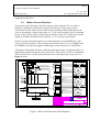
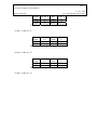
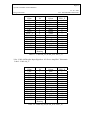
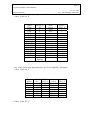
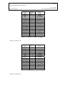
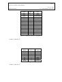
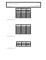
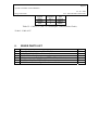
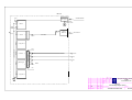
E U R O P E A N S O U T H E R N O B S E R V A T ORY
Organisation Européenne pour des Recherches Astronomiques dans l'Hémisphère Austral
Europäische Organisation für astronomische Forschung in der südlichen Hemisphäre
LA SILLA OBSERVATORY
3p6 M2 CONTROL ELECTRONICS
Doc. No.: 3P6-DSD-ESO-60400-0001
Issue: 2.0
Date: 24 – January - 2005
Prepared: J. Alonso
Name
Date
Signature
Date
Signature
Approved: G. Andreoni
Name
Released: G. Andreoni
Name
Date
Signature
Page 2
3p6 M2 CONTROL ELECTRONICS
24 - 06 - 2005
Doc. 3P6-DSD-ESO-60400-0001
Design Document
CHANGE RECORD
Revision
Date
Section/Paragraph
Remarks
Issue 1
Issue 1.1
28/05/2004
25/06/2004
First Issue
Issue 2.0
24/01/2005
All
Several corrections,
additions.
Mains power
distribution modification
Several corrections
Section 3 Focus, X and
Y limit range.
Focus Mitutoyo
Available spare parts list
added.
As built
Page 3
3p6 M2 CONTROL ELECTRONICS
24 - 06 - 2005
Doc. 3P6-DSD-ESO-60400-0001
Design Document
INDEX OF CONTENTS
1.
INTRODUCTION .............................................................................................................................5
1.1.
1.2.
1.3.
1.4.
2.
M2 MOTION CONTROL ................................................................................................................7
2.1.
2.2.
2.3.
2.4.
3.
FOCUS, X AND Y DRIVE COMPONENTS ......................................................................................10
FOCUS LINEAR ENCODER ...........................................................................................................11
ELECTRONICS CABINET...........................................................................................................11
4.1.
4.2.
4.3.
4.4.
4.5.
5.
MOTION CONTROL CONCEPT........................................................................................................7
MOTION CONTROL COMPONENTS.................................................................................................7
MOTION CONTROL FUNCTIONS ....................................................................................................8
FOCUS, X AND Y POSITION AND VELOCITY CONTROL LOOPS ........................................................9
M2 DRIVES ELECTROMECHANICAL COMPONENTS .......................................................10
3.1.
3.2.
4.
PURPOSE AND SCOPE.............................................................................................................5
REFERENCE DOCUMENTS.....................................................................................................5
APPLICABLE DOCUMENTS ...................................................................................................5
ACRONYMS & ABBREVIATIONS..........................................................................................6
VME LCU .................................................................................................................................11
AC SERVO AMPLIFIERS ..............................................................................................................11
VME4SA COMPONENT ADAPTER CONFIGURATION ...................................................................11
CABINET COOLING UNIT ............................................................................................................12
MAINS POWER DISTRIBUTION ....................................................................................................12
CABLING ........................................................................................................................................13
5.1. FOCUS, X AN Y DRIVE UNITS ......................................................................................................13
5.2. CABINET .....................................................................................................................................13
5.2.1.
Cable Feed-trough.............................................................................................................13
5.3. INSIDE THE LCU.........................................................................................................................13
5.4. WIRING TABLES .........................................................................................................................13
6.
SPARE PARTS LIST......................................................................................................................25
7.
DRAWING AND SCHEMATIC DIAGRAM APPENDIX .........................................................26
7.1.
7.2.
7.3.
7.4.
7.5.
7.6.
7.7.
7.8.
7.9.
7.10.
7.11.
7.12.
BLOCK DIAGRAM .......................................................................................................................26
M2-LCU CHASSIS LAYOUT .......................................................................................................26
M2-LCU INTERNAL WIRING DIAGRAM (PART 1).......................................................................26
M2-LCU INTERNAL WIRING DIAGRAM (PART 2).......................................................................26
M2 RACK LAYOUT REAR VIEW..................................................................................................26
CABLING LAYOUT ......................................................................................................................26
CABLE #1 VME4SA TO SERVO AMPLIFIER AND CONDITIONING PCB .......................................26
CABLE #2 TERMINAL STRIP TO SERVO AMPLIFIER .....................................................................26
CABLE #4 ENCODER INPUT SIGNALS TO AC-SERVO AMPLIFIER ................................................26
LIMIT SWITCHES SIGNAL CONDITIONING CIRCUIT .................................................................26
LIMIT SWITCHES SIGNAL CONDITIONING PCB .......................................................................26
FOCUS MITUTOYO LINEAR ENCODER CONNECTION ...............................................................26
INDEX OF FIGURES AND TABLES
FIGURE 1: M2 CONTROL ELECTRONICS BLOCK DIAGRAM ...........................................................................8
Page 4
3p6 M2 CONTROL ELECTRONICS
Design Document
24 - 06 - 2005
Doc. 3P6-DSD-ESO-60400-0001
TABLE 1: FHA-25B-3015E-E150 HARMONIC DRIVE ................................................................................10
TABLE 2 : ABSOLUTE MAXIMUM MECHANICAL TRAVEL ...........................................................................10
TABLE 3 : COMPONENT ADAPTER CONFIGURATION ...................................................................................12
TABLE 4 : CABLE #1_F* (CHANNEL #1 VME4SA TO TSC1_F, ACSA_F, LSWC_F) ...............................13
TABLE 5 : CABLE #1_X* (CHANNEL #2 VME4SA TO TSC1_X, ACSA_X, LSWC_X).............................14
TABLE 6 : CABLE #1_Y* (CHANNEL #3 VME4SA TO TSC1_Y, ACSA_Y, LSWC_Y).............................14
TABLE 7 : CABLE #2_F*(TSC1_F TO ACSA_F) ........................................................................................15
TABLE 8 : CABLE #2_X*(TSC1_X TO ACSA_X) ......................................................................................15
TABLE 9 : CABLE #2_X*(TSC1_Y TO ACSA_Y) ......................................................................................15
TABLE 10 : CABLE #3_F*(ACSA_F TO LSWC_F) ....................................................................................16
TABLE 11 : CABLE #3_X*(ACSA_X TO LSWC_X) ..................................................................................16
TABLE 12 : CABLE #3_Y*(ACSA_Y TO LSWC_Y) ..................................................................................16
TABLE 13 : CABLE #4_F*(ACSA_F TO TSU1_F)......................................................................................17
TABLE 14 : CABLE #4_X*(ACSA_X TO TSU1_X)....................................................................................17
TABLE 15 : CABLE #4_Y*(ACSA_Y TO TSU1_Y)....................................................................................18
TABLE 16 : CABLE #5_F*(ACSA_F & TSC2_F TO TSU2_F)....................................................................18
TABLE 17 : CABLE #5_X*(ACSA_X & TSC2_X TO TSU2_X).................................................................19
TABLE 18 : CABLE #5_Y*(ACSA_Y & TSC2_Y TO TSU2_Y).................................................................19
TABLE 19 : CABLE #6_F*(LSWC_F TO TSU3_F) .....................................................................................19
TABLE 20 : CABLE #6_X*(LSWC_X TO TSU3_X) ...................................................................................20
TABLE 21 : CABLE #6_Y*(LSWC_Y TO TSU3_Y) ...................................................................................20
TABLE 22 : CABLE #7*(TSC1 TO TSU1)....................................................................................................20
TABLE 23 : CABLE #8_F*(TSU1_F TO HD_F)...........................................................................................21
TABLE 24 : CABLE #8_X*(TSU1_X TO HD_X).........................................................................................21
TABLE 25 : CABLE #8_Y*(TSU1_Y TO HD_Y).........................................................................................22
TABLE 26 : CABLE #9_F*(TSU2_F TO HD_F)...........................................................................................22
TABLE 27 : CABLE #9_X*(TSU2_X TO HD_X).........................................................................................23
TABLE 28 : CABLE #9_Y*(TSU2_Y TO HD_Y).........................................................................................23
TABLE 29 : CABLE #10_F*(TSU3_F TO UL_F) .........................................................................................23
TABLE 30 : CABLE #10_X*(TSU3_X TO UL_X) .......................................................................................24
TABLE 31 : CABLE #10_Y*(TSU3_Y TO UL_Y) .......................................................................................24
TABLE 32 : CABLE #11_F*(TSU3_F TO LL_F) .........................................................................................24
TABLE 33 : CABLE #11_X*(TSU3_X TO LL_X) .......................................................................................24
TABLE 34 : CABLE #11_Y*(TSU3_Y TO LL_Y) .......................................................................................24
TABLE 35 : CABLE #12*(TSU1 TO CATASTROPHIC LIMIT SWITCHES CHAIN) ............................................25
Page 5
3p6 M2 CONTROL ELECTRONICS
Design Document
1.
24 - 06 - 2005
Doc. 3P6-DSD-ESO-60400-0001
INTRODUCTION
Since ever the 3.6 telescope f/8 secondary unit has suffered from severe mechanical
instabilities. This together with the inability to introduce online corrections to the
decentring comma has severely limited the optical performance of the telescope.
Considering that the new generation of instruments (e.g. HARPS) need to exploit the
maximum possible optical image quality attainable with the telescope, a new
mechanical design based on the NTT secondary unit concept was designed and built.
The new unit is equipped with VLT complaint computer controlled servo drives for the
focus, X and Y motions of the secondary mirror unit.
1.1.
PURPOSE AND SCOPE
This document is intended to serve as a design document, construction guide and
service manual for the 3p6 M2 control electronics.
Starting from a general description and block diagram it goes all the way down to the
schematic diagrams, function tables, connection tables and references to the part list.
1.2.
[RE1]
[RE2]
1.3.
[AP1]
[AP2]
[AP3]
[AP4]
[AP5]
[AP6]
REFERENCE DOCUMENTS
3.6m Telescope f/8 Top-end Overhaul User Requirements 3p6-SPEESO-36022-0001 Issue 1.3 M. Sterzik December 12, 2001.
Configuration of VLT Standard VME Boards VLT-MAN-ESO-172101358 Issue 1.4 B. Gustafsson 5-October-2001
APPLICABLE DOCUMENTS
ESO VME4SA-X1 4-Channel DC Servo Amplifier Technical Manual
VLT-MAN-ESO-17130-0273 Issue 3.0
ESO VME4SA BACKPLANE Technical Manual VLT-MAN-ESO17130-0274 Issue 3.0
VLT Electronic Cabinet Cooling System User Manual VLT-MAN-ESO17130-1603 Issue 1.0 F. Biancat Marchet April 27, 1998
USER-Manual MACCONTROLLER MAC4-INC Version 4.2
Harmonic Drive Operations Manual AC-Servo Amplifier SC-500/510.
VLT-SPE-ESO-10000-0015 VLT Electronic Design Specification Issue
4.0 09/12/96.
Page 6
3p6 M2 CONTROL ELECTRONICS
24 - 06 - 2005
Doc. 3P6-DSD-ESO-60400-0001
Design Document
1.4.
DC
VME
TBD
TBM
VLT
LCU
NTT
PCB
RAM
TTL
PPR
ZD
ACRONYMS & ABBREVIATIONS
Direct Current
Versa Module Europe
To Be Defined
To Be Measured
Very Large Telescope
Local Control Unit
New Technology Telescope
Printed Circuit Board
Random Access Memory
Transistor Transistor Logic
Pulse Per Revolution
Zenith Distance
Page 7
3p6 M2 CONTROL ELECTRONICS
Design Document
2.
24 - 06 - 2005
Doc. 3P6-DSD-ESO-60400-0001
M2 MOTION CONTROL
2.1. Motion Control Concept
The concept developed for the motion control of the 3p6 M2 unit is based on the
standard motion control components used by ESO to build instruments. This approach
brings various advantages like: reduced development and manufacturing costs, past
proven experience, standardised components and shared spare parts.
The standard VME4SA is used as usually done with the MACC-INC companion. The
difference with the more typical implementations is that here the VME4SA does not act
as the drive motor power amplifier but as a signal driver for a specialized, high power,
AC servo amplifier. However the limit and init switches interface capabilities of the
VME4SA are still fully used. The advantage of this approach is that the specialized AC
servo amplifier is absolutely transparent to the VLT software.
2.2. Motion Control Components
The motion control electronic components used for the M2 are:
¾ MACC4/INC [AP4] and VME-4SA [AP1] VLT standard modules.
¾ Harmonic Drive AC-Servo Amplifier SC500/510 [AP5]
Three Harmonic Drive Systems servo actuators type FHA-25B-3015E-E150 are used
for rotating the focus, X and Y driving screws. These actuators integrate a brushless
AC motor together with a harmonic reduction gear and an incremental 1500 PPR
optical shaft encoder coupled to the motor axis. Each linear drive is complemented by
end of stroke high precision limit/init switches together with coarse catastrophic-limit
switches.
Every actuator is accompanied by three screw terminals group. All the connections
from the actuator and limit/init switches are routed trough these terminals to the control
LCU-power amplifiers cabinet. The signal groups correspond to; AC motor drive,
incremental encoder and limit/init switches.
The control electronics is mounted on top of the M2 unit inside a hermetically sealed
Knürr cabinet equipped with an active heat exchanger unit. The cabinet houses a VME
LCU, three AC servo amplifiers and support circuitry.
Externally the control cabinet receives; the mains 220VAC supply, the Ethernet
connection, one inlet and one outlet coolant hoses. By opening the rear door an external
PC could be connected via RS232 to each AC servo amplifier and the LCU console
port. This is for setup and engineering monitoring of the servo amplifiers and VME
CPU configuration.
Page 8
3p6 M2 CONTROL ELECTRONICS
24 - 06 - 2005
Doc. 3P6-DSD-ESO-60400-0001
Design Document
From the control cabinet three identical groups of signals are routed to its close
neighbour the M2 drive.
2.3. Motion Control Functions
The motion control function of the M2 comprises three identical AC servo drives
amplifier combinations with built in digital velocity loop. These units provide
incremental encoder pulses to the outside world as balanced differential signals and
receives an analogue voltage in the range of +/-10V as the external velocity command.
On top of the velocity loop a position loop inside the control LCU utilizes the encoder
signals as feedback and delivers the required +/-10V velocity control signal.
Normal operation init/limit functions are implemented by six BAUMER type “MyCom g” precision switches. These switches report both to the AC servo amplifier and
the VME4SA via dedicated signal conditioning circuits mounted over small PCBs.
A hardware interlocking function, called the catastrophic limit, is implemented by six
rugged limit switches mounted at the end of stroke for the focus, X and Y mechanisms.
The six switches are serially connected and act over the mains power relay coil, see
Figure 1 below.
RS-232
Limit SW.
FOCUS
ENCODER, ANALOGUE DRIVE and LIMIT SIGNALS
SERVO AMP.
Velocity
Controller
ENCODER, ANALOGUE DRIVE and LIMIT SIGNALS
ENCODER
POWER DRIVE
Regeneration Resistor
47Ohms 50W
HARMONIC
DRIVE
M2 LCU
Limit Switches
Conditioning
VME-4SA-1
Servo Amps.
Limit SW.
Limit Switches
Conditioning
ENCODER, ANALOGUE DRIVE and LIMIT SIGNALS
INCREMENTAL ENCODER SIGNALS
MAC INC
RS-232
CATASTROPHIC LIMIT CIRCUIT
VxWorks Console
Catastrophic Limit Circuit
SCHUKO RECEPTACLES
MVME167 CPU
RS-232
RFI POWER
LINE FILTER
FUSE
230V Supply + PE
Ethernet
(Dimensions 578X555X800mm - Power dissipation ~500W)
Power
Relay
SURGE
ARRESTOR
+
Inrush Supressor
M2 MECHANICS
M2 TOP UNIT MINI RACK
THERMOSTAT
EXTERNAL
BREAKER
Limit SW.
SERVO AMP.
Velocity
Controller
POWER DRIVE
X
ENCODER
INCREMENTAL ENCODER SIGNALS
RS-232
Limit SW.
Regeneration Resistor
47Ohms 50W
HARMONIC
DRIVE
Catastrophic Limit Circuit
Limit SW.
Limit Switches
Conditioning
COOLANT
FLUID
ESO Standard Cooling Unit
SERVO AMP.
Velocity
Controller
POWER DRIVE
ENCODER
INCREMENTAL ENCODER SIGNALS
Regeneration Resistor
47Ohms 50W
INTERNAL TEMP. SENSOR
Date
Drawn
Chckd.
Appr.
EXTERNAL TEMP. SENSOR
01/05/03
Limit SW.
Init.
JA
Title:
Y
HARMONIC
DRIVE
European Southern Observatory
3.6 M2
Control Electronics
Page
Block Diagram
1/1
1
Issue
FDR
Revisions
06/05/03 JA
Date
Init
Document Number:
File Name:
3P6-DSD-ESO-60400-0001
Figure 1: M2 Control Electronics Block Diagram
M2block1.skf
Page 9
3p6 M2 CONTROL ELECTRONICS
Design Document
24 - 06 - 2005
Doc. 3P6-DSD-ESO-60400-0001
2.4. Focus, X and Y Position and velocity control loops
The rotation and angular positioning of the M2 drive screws is performed by means of
nested position and velocity control loops.
The main loop is the position control loop starting with an incremental encoder to sense
the relative angular position of the motor. A dedicated VME motion controller
MAC4/INC [AP4] compares the sensed position with the position command value
calculated by the main instrument control software and generates a corrective action
(+/-10VDC range) to the AC servo amplifier [AP5]. The configuration software sets the
position controller parameters like integration gain, maximum speed, software limits,
initialization point, etc.
The second loop is the velocity control loop. The corrective output signal (± 10V)
generated by the position control loop is sent to the AC servo amplifier trough the
VME driver-amplifier VME4SA [AP1], this is to have all the limit and init switches
signals compatible with the VLT software. The AC motor velocity is measured by
means of the same incremental encoder coupled to the motor axis used to measure the
screw angular position. The velocity value is compared with the commanded velocity
value coming from the MAC4/INC output and the error signal is filtered by a digital
PID inside the servo amplifier. The PID filter parameters are defined by the aid of a MS
Windows program talking via RS232 to the amplifier during configuration. The
parameters are kept in a flash memory inside the amplifier.
Each function, focus, X and Y is equipped with limit/init and catastrophic limit
switches mounted at the end of stroke of each function. The mechanical configuration
is such that during normal operation the limit/init switches are only actuated but in case
of malfunction the carriage will continue moving actuating the catastrophic limit switch
as well.
Page 10
3p6 M2 CONTROL ELECTRONICS
24 - 06 - 2005
Doc. 3P6-DSD-ESO-60400-0001
Design Document
3.
M2 DRIVES ELECTROMECHANICAL COMPONENTS
3.1. Focus, X and Y Drive Components
All three axis use identical electromechanical components.
Rated Output Power
Rated Output Torque
Maximum Output Torque
Max. Continuous Stall Torque
Rated Output Speed
Maximum Output Speed
Rated Current
Maximum Current
Ratio
Torque Constant
Voltage Constant
Mechanical Time Constant
Electrical Time Constant
Moment of Inertia (output)
Power Supply for control Unit
Rated Motor Speed
Maximum Motor Speed
Resistance
Inductance
Weight
Encoder Resolution
Encoder Output Signals
W
Nm
Nm
Nm
Rpm
Rpm
Arms
Arms
Nm/A
V/Rpm
mS
mS
Kgm²
VAC
Rpm
Rpm
Ω
mH
Kg
Ppr
-
160
51
157
71
30
40
1.4
3.2
100
60
6.4
6.8
1.4
2.3
230
3000
4000
3.7
5
4.7
1500
A,A\,B,B\,C,C\,U,U\,V,V\W,W\.
5V Line Driver
Table 1: FHA-25B-3015E-E150 Harmonic Drive
•
•
•
The init-limit switches are BAUMER type “My-Com g”.
The catastrophic limit switches are Omron type D4D-1532N.
The driving screws are of the zero backlash type equipped with roller screw
nuts. The pitch is 1 millimetre.
Focus
X
Y
mm
mm
mm
+/- 20
+/- 6.2
+/- 6.5
Table 2 : Absolute Maximum Mechanical Travel
•
The focus limit switches adjustment is set to +/-16mm for the normal limit and
+/-16.5mm for the focus catastrophic limit.
Page 11
3p6 M2 CONTROL ELECTRONICS
Design Document
•
24 - 06 - 2005
Doc. 3P6-DSD-ESO-60400-0001
The X and Y limit switches adjustment is set to +/-5mm for the normal limit
and +/-5.5mm for the X and Y catastrophic limit.
3.2. Focus Linear Encoder
Originally the three axes focus, X and Y were equipped with rotary encoders inside the
AC servo drive actuators. These actuators drive the mechanism screw directly and
assume that the screw-nut combination is backlash free. From these encoders the
velocity and position feedback for the control system is derived.
During the preliminary tests we found that the focus screw-nut combination has a
backlash greater than 100um. It was decided to keep the rotary encoder for the velocity
feedback and add a linear 45mm stroke 1um resolution, 2um precision Mitutoyo
encoder, measuring directly over the focus carriage, for the focus position feedback.
Refer to 7.12 for the connection details.
4.
Electronics Cabinet
The control electronics is mounted on top of the M2 unit inside a hermetically sealed
Knürr cabinet equipped with an active heat exchanger unit. The cabinet houses a VME
LCU, three AC servo amplifiers and support circuitry.
4.1. VME LCU
The VME LCU is integrated by the following components:
¾ ESO standard VME RACK (with minimized depth)
¾ 10 Slots VMEBUS with Active Termination and Auto Daisy Chain
¾ MVME 712M Transition Module for the CPU I/O
¾ MVME 2604 Power PC 604 32-bit microprocessor 32MB RAM memory
¾ MAC4/INC MACCON Motion Controller Module [AP4]
¾ VME4SA-I ESO DC Servo Amplifier type 1 (2 Amps capacity) [AP1]
¾ 2X KNIEL 15V 1.6A DC Power Supply.
¾ VME Power Supply KNIEL FPM 300W.
Refer to 7.2 7.3 7.4 drawings for a schematic view of the VME LCU.
4.2. AC Servo Amplifiers
Three AC Servo Amplifiers type SC-510 are mounted inside the cabinet as shown on
7.5. Refer to [AP5] for a detail description of the SC-510.
4.3. VME4SA Component Adapter Configuration
For each channel the VME4SA has an eight pin dual in line socket for plug in a small
component carrier whose components are dependent on the application, refer to [AP1]
page 8 for a detailed explanation.
In this application the configuration for channels 1, 2 and 3 is identical and as shown in
the table below:
Pin # row 1 Pin # row 2 Component
1
8
Open
2
7
360K
Page 12
3p6 M2 CONTROL ELECTRONICS
24 - 06 - 2005
Doc. 3P6-DSD-ESO-60400-0001
Design Document
3
4
6
5
Wire jumper
Open
Table 3 : Component Adapter Configuration
4.4. Cabinet Cooling Unit
The cabinet cooling unit used is the ESO standard “VLT Electronic Cabinet Cooling
System” [AP3]. The unit is mounted on the bottom of the cabinet with adequate
clearance around it for the proper air circulation. Two PT100 elements, one mounted
over a heat-sink in the outer wall of the cabinet and the other in contact with the inner
wall of the cabinet, are used by the cooling system for keeping the internal temperature
the same as the exterior and thus avoiding thermal gradients. The heat is removed from
the unit by means of circulating water.
Note that the cooling unit fans are used for blowing air directly over the VME chassis,
due to space limitations no supplemental fan tray is used in the application.
4.5. Mains Power Distribution
AC power enters the cabinet via a double pole circuit breaker. The control knob of this
breaker is located externally over the side wall of the cabinet. Internally the AC supply
goes to a double contact power relay. The coil of the relay is energized with the mains
supply and serially connected with the catastrophic limit switches chain a thermostat
and a protection fuse. Finally the mains supply goes through an inrush suppressor an
over-voltage protector and a power line filter. The power distribution after the
conditioning is as follows:
¾ Direct connection to the three AC servo amplifiers.
¾ Three Schucko outlets for powering the VME, cooling unit and spare.
Refer to 7.6 for the schematic diagram.
Page 13
3p6 M2 CONTROL ELECTRONICS
Design Document
5.
24 - 06 - 2005
Doc. 3P6-DSD-ESO-60400-0001
CABLING
5.1. Focus, X an Y drive units
Near each harmonic drive unit a group of three numbered screw terminal strips named
TSU1_n, TSU2_n and TSU3_n, where n is F,X,Y, to identify the particular group,
serve both as test points and junction for the connections coming from the LCU cabinet
to each harmonic drive unit and limit-init switches.
5.2. Cabinet
The cabinet wiring is as shown on 7.6. For sake of simplicity only one channel is
shown.
5.2.1. Cable Feed-trough
The cables feed-trough is a custom built piece which allows passing every cable and
hose to the cabinet interior keeping adequate seal to prevent the internally circulating
air of leaking to the outside environment.
5.3. Inside the LCU
The LCU wiring is done as shown on 7.3 and 7.4.
5.4.
Wiring Tables
Signal
Pin #
Pairs
Term # ACSA_F LSWC_F
VME4SA VME4SA Colour TSC1_F
X3
J1
M+
E8
Red
1
ME5
Black
2
Shield #1
3**
Shield #2
1
Phase +A
A8
Pink
2
Phase -A
A6
Grey
3
Phase +B
B7
Yellow
4
Phase -B
B5
Green
5
Phase +Z
A4
White
6
Phase -Z
A2
Brown
7
Upp. Lim
C3
Violet
3
Low. Lim
D3
Black
7
GND
C6
Blue
7
10
Vx(+15V)
D2
Red
9
9
Table 4 : Cable #1_F* (Channel #1 VME4SA to TSC1_F, ACSA_F, LSWC_F)
*See “Cable #1 VME4SA to Servo Amplifier and Conditioning PCB” Schematic.
Label: “Cable #1_F”.
**Shield #1 connected to terminal #3 in series with a 51ohm resistor and 10nF
capacitor (see “Cabling Layout” Schematic).
Page 14
3p6 M2 CONTROL ELECTRONICS
Design Document
24 - 06 - 2005
Doc. 3P6-DSD-ESO-60400-0001
Signal
Pin #
Pairs
Term # ACSA_X LSWC_X
VME4SA VME4SA Colour TSC1_X
X3
J1
M+
E8
Red
1
ME5
Black
2
Shield #1
3**
Shield #2
1
Phase +A
A8
Pink
2
Phase -A
A6
Grey
3
Phase +B
B7
Yellow
4
Phase -B
B5
Green
5
Phase +Z
A4
White
6
Phase -Z
A2
Brown
7
Upp. Lim
C3
Violet
3
Low. Lim
D3
Black
7
GND
C6
Blue
7
10
Vx(+15V)
D2
Red
9
9
Table 5 : Cable #1_X* (Channel #2 VME4SA to TSC1_X, ACSA_X, LSWC_X)
*See “Cable #1 VME4SA to Servo Amplifier and Conditioning PCB” Schematic.
Label: “Cable #1_X”.
**Shield #1 connected to terminal #3 in series with a 51ohm resistor and 10nF
capacitor (see “Cabling Layout” Schematic).
Signal
Pin #
Pairs
Term # ACSA_Y LSWC_Y
VME4SA VME4SA Colour TSC1_Y
X3
J1
M+
E8
Red
1
ME5
Black
2
Shield #1
3**
Shield #2
1
Phase +A
A8
Pink
2
Phase -A
A6
Grey
3
Phase +B
B7
Yellow
4
Phase -B
B5
Green
5
Phase +Z
A4
White
6
Phase -Z
A2
Brown
7
Upp. Lim
C3
Violet
3
Low. Lim
D3
Black
7
GND
C6
Blue
7
10
Vx(+15V)
D2
Red
9
9
Table 6 : Cable #1_Y* (Channel #3 VME4SA to TSC1_Y, ACSA_Y, LSWC_Y)
*See “Cable #1 VME4SA to Servo Amplifier and Conditioning PCB” Schematic.
Label: “Cable #1_Y”.
**Shield #1 connected to terminal #3 in series with a 51ohm resistor and 10nF
capacitor (see “Cabling Layout” Schematic).
Page 15
3p6 M2 CONTROL ELECTRONICS
24 - 06 - 2005
Doc. 3P6-DSD-ESO-60400-0001
Design Document
Signal
Term #
Pairs ACSA_F
Name
TSC1_F Colour
X7
Shield
1
9
Phase +A
2
Pink
1
Phase -A
3
Grey
6
Phase +B
4
Yellow
2
Phase -B
5
Green
7
Phase +Z
6
White
3
Phase -Z
7
Brown
8
Table 7 : Cable #2_F*(TSC1_F to ACSA_F)
*See “Cable #2 Terminal Strip to Servo Amplifier” Schematic.
Label: “Cable #2_F”.
Signal
Term #
Pairs ACSA_X
Name
TSC1_X Colour
X7
Shield
1
9
Phase +A
2
Pink
1
Phase -A
3
Grey
6
Phase +B
4
Yellow
2
Phase -B
5
Green
7
Phase +Z
6
White
3
Phase -Z
7
Brown
8
Table 8 : Cable #2_X*(TSC1_X to ACSA_X)
*See “Cable #2 Terminal Strip to Servo Amplifier” Schematic.
Label: “Cable #2_X”.
Signal
Term #
Pairs ACSA_Y
Name
TSC1_Y Colour
X7
Shield
1
9
Phase +A
2
Pink
1
Phase -A
3
Grey
6
Phase +B
4
Yellow
2
Phase -B
5
Green
7
Phase +Z
6
White
3
Phase -Z
7
Brown
8
Table 9 : Cable #2_X*(TSC1_Y to ACSA_Y)
*See “Cable #2 Terminal Strip to Servo Amplifier” Schematic.
Label: “Cable #2_Y”.
Page 16
3p6 M2 CONTROL ELECTRONICS
24 - 06 - 2005
Doc. 3P6-DSD-ESO-60400-0001
Design Document
Signal ACSA_F
Pair
LSWC_F
Name
X3
Colour
J1
CCWL
11
Violet
4
CWL
10
Black
8
Table 10 : Cable #3_F*(ACSA_F to LSWC_F)
*Label: “Cable #3_F”.
Signal ACSA_X
Pair
LSWC_X
Name
X3
Colour
J1
CCWL
11
Violet
4
CWL
10
Black
8
Table 11 : Cable #3_X*(ACSA_X to LSWC_X)
*Label: “Cable #3_X”.
Signal ACSA_Y
Pair
LSWC_Y
Name
X3
Colour
J1
CCWL
11
Violet
4
CWL
10
Black
8
Table 12 : Cable #3_Y*(ACSA_Y to LSWC_Y)
*Label: “Cable #3_Y”.
Page 17
3p6 M2 CONTROL ELECTRONICS
24 - 06 - 2005
Doc. 3P6-DSD-ESO-60400-0001
Design Document
Signal
ACSA_F
Pairs
Term #
Name
CHA
CHA/
CHB
CHB/
CHC
CHC/
SYNC_U
SYNC_U/
SYNC_V
SYNC_V/
SYNC_W
SYNC_W/
+5V(Enc)
DGND
Shield
X9
1
6
2
7
3
8
4
5
10
15
9
14
11
13
D-Sub
Housing
Colour
Pink
Grey
Yellow
Green
White
Brown
Violet
Black
White/green
Brown/green
Red/blue
Grey/pink
Red
Blue
TSU1_F
1
2
3
4
5
6
7
8
9
10
11
12
13
14
15
Table 13 : Cable #4_F*(ACSA_F to TSU1_F)
*See “Cable #4 Encoder Input Signals to AC-Servo Amplifier” Schematic.
Label: “Cable #4_F”.
Signal
Name
CHA
CHA/
CHB
CHB/
CHC
CHC/
SYNC_U
SYNC_U/
SYNC_V
SYNC_V/
SYNC_W
SYNC_W/
+5V(Enc)
DGND
Shield
ACSA_X
Pairs
Term #
X9
Colour
TSU1_X
1
Pink
1
6
Grey
2
2
Yellow
3
7
Green
4
3
White
5
8
Brown
6
4
Violet
7
5
Black
8
10
White/green
9
15
Brown/green
10
9
Red/blue
11
14
Grey/pink
12
11
Red
13
13
Blue
14
D-Sub
15
Housing
Table 14 : Cable #4_X*(ACSA_X to TSU1_X)
Page 18
3p6 M2 CONTROL ELECTRONICS
24 - 06 - 2005
Doc. 3P6-DSD-ESO-60400-0001
Design Document
*See “Cable #4 Encoder Input Signals to AC-Servo Amplifier” Schematic.
Label: “Cable #4_X”.
Signal
Name
CHA
CHA/
CHB
CHB/
CHC
CHC/
SYNC_U
SYNC_U/
SYNC_V
SYNC_V/
SYNC_W
SYNC_W/
+5V(Enc)
DGND
Shield
ACSA_Y
Pairs
Term #
X9
Colour
TSU1_Y
1
Pink
1
6
Grey
2
2
Yellow
3
7
Green
4
3
White
5
8
Brown
6
4
Violet
7
5
Black
8
10
White/green
9
15
Brown/green
10
9
Red/blue
11
14
Grey/pink
12
11
Red
13
13
Blue
14
D-Sub
15
Housing
Table 15 : Cable #4_Y*(ACSA_Y to TSU1_Y)
*See “Cable #4 Encoder Input Signals to AC-Servo Amplifier” Schematic.
Label: “Cable #4_Y”.
Signal ACSA_F TERM # Cables
Term #
Name
X1
TSC2_F Colour TSU2_F
Brk1
1
Brown
1
Brk2
2
White
2
U
U
Yellow
3
V
V
Grey
4
W
W
Pink
5
PE
PE
Green
6
PE
PE
Shield
7
Table 16 : Cable #5_F*(ACSA_F & TSC2_F to TSU2_F)
*Label: “Cable #5_F”.
Page 19
3p6 M2 CONTROL ELECTRONICS
24 - 06 - 2005
Doc. 3P6-DSD-ESO-60400-0001
Design Document
Signal ACSA_X TERM # Cables
Term #
Name
X1
TSC2_X Colour TSU2_X
Brk1
1
Brown
1
Brk2
2
White
2
U
U
Yellow
3
V
V
Grey
4
W
W
Pink
5
PE
PE
Green
6
PE
PE
Shield
7
Table 17 : Cable #5_X*(ACSA_X & TSC2_X to TSU2_X)
*Label: “Cable #5_X”.
Signal ACSA_Y TERM # Cables
Term #
Name
X1
TSC2_Y Colour TSU2_Y
Brk1
1
Brown
1
Brk2
2
White
2
U
U
Yellow
3
V
V
Grey
4
W
W
Pink
5
PE
PE
Green
6
PE
PE
Shield
7
Table 18 : Cable #5_Y*(ACSA_Y & TSC2_Y to TSU2_Y)
*Label: “Cable #5_Y”.
Signal LSWC_F
Pairs
TERM #
Name
J1
Colour TSU3_F
Shield
Earth
Earth
SWC3A
1
White
1
SWC3B
2
Yellow
2
SWD3A
5
Brown
3
SWD3B
6
Green
4
Table 19 : Cable #6_F*(LSWC_F to TSU3_F)
*Label: “Cable #6_F”.
Page 20
3p6 M2 CONTROL ELECTRONICS
24 - 06 - 2005
Doc. 3P6-DSD-ESO-60400-0001
Design Document
Signal LSWC_X
Pairs
TERM #
Name
J1
Colour TSU3_X
Shield
Earth
Earth
SWC3A
1
White
1
SWC3B
2
Yellow
2
SWD3A
5
Brown
3
SWD3B
6
Green
4
Table 20 : Cable #6_X*(LSWC_X to TSU3_X)
*Label: “Cable #6_X”.
Signal LSWC_Y
Pairs
TERM #
Name
J1
Colour TSU3_Y
Shield
Earth
Earth
SWC3A
1
White
1
SWC3B
2
Yellow
2
SWD3A
5
Brown
3
SWD3B
6
Green
4
Table 21 : Cable #6_Y*(LSWC_Y to TSU3_Y)
*Label: “Cable #6_Y”.
Signal TERM # Cables TERM #
Name
TSC1
Colour
TSU1
Neutral
1
White
1
F20
2
Black
2
Table 22 : Cable #7*(TSC1 to TSU1)
*Label: “Cable #7”.
Page 21
3p6 M2 CONTROL ELECTRONICS
24 - 06 - 2005
Doc. 3P6-DSD-ESO-60400-0001
Design Document
Signal
Name
CHA
CHA/
CHB
CHB/
CHC
CHC/
SYNC_U
SYNC_U/
SYNC_V
SYNC_V/
SYNC_W
SYNC_W/
+5V(Enc)
DGND
Shield
TERM #
TSU1_F
1
2
3
4
5
6
7
8
9
10
11
12
13
14
15
Pairs
Colour
Green
Green/white
Grey
Grey/white
Yellow
Yellow/white
Brown
Brown/white
Blue
Blue/white
Orange
Orange/white
Red
Black
Table 23 : Cable #8_F*(TSU1_F to HD_F)
*Label: “Cable #8_F”.
Signal
TERM #
Pairs
Name
TSU1_X
Colour
CHA
1
Green
CHA/
2
Green/white
CHB
3
Grey
CHB/
4
Grey/white
CHC
5
Yellow
CHC/
6
Yellow/white
SYNC_U
7
Brown
SYNC_U/
8
Brown/white
SYNC_V
9
Blue
SYNC_V/
10
Blue/white
SYNC_W
11
Orange
SYNC_W/
12
Orange/white
+5V(Enc)
13
Red
DGND
14
Black
Shield
15
Table 24 : Cable #8_X*(TSU1_X to HD_X)
*Label: “Cable #8_X”.
Page 22
3p6 M2 CONTROL ELECTRONICS
24 - 06 - 2005
Doc. 3P6-DSD-ESO-60400-0001
Design Document
Signal
Name
CHA
CHA/
CHB
CHB/
CHC
CHC/
SYNC_U
SYNC_U/
SYNC_V
SYNC_V/
SYNC_W
SYNC_W/
+5V(Enc)
DGND
Shield
TERM #
TSU1_Y
1
2
3
4
5
6
7
8
9
10
11
12
13
14
15
Pairs
Colour
Green
Green/white
Grey
Grey/white
Yellow
Yellow/white
Brown
Brown/white
Blue
Blue/white
Orange
Orange/white
Red
Black
Table 25 : Cable #8_Y*(TSU1_Y to HD_Y)
*Label: “Cable #8_Y”.
Signal
TERM #
Cables
Name
TSU2_F
Colour
Brk1
1
Blue
Brk2
2
Yellow
U
3
Red
V
4
Black
W
5
White
PE
6
Green
Shield
7
Shield
Table 26 : Cable #9_F*(TSU2_F to HD_F)
*Label: “Cable #9_F”.
Page 23
3p6 M2 CONTROL ELECTRONICS
24 - 06 - 2005
Doc. 3P6-DSD-ESO-60400-0001
Design Document
Signal
TERM #
Cables
Name
TSU2_X
Colour
Brk1
1
Blue
Brk2
2
Yellow
U
3
Red
V
4
Black
W
5
White
PE
6
Green
Shield
7
Shield
Table 27 : Cable #9_X*(TSU2_X to HD_X)
*Label: “Cable #9_X”.
Signal
TERM #
Cables
Name
TSU2_Y
Colour
Brk1
1
Blue
Brk2
2
Yellow
U
3
Red
V
4
Black
W
5
White
PE
6
N/A
Shield
7
Shield
Table 28 : Cable #9_Y*(TSU2_Y to HD_Y)
*Label: “Cable #9_Y”.
Signal
TERM #
Pair
Name
TSU3_F
Colour
SWC3A
1
Black
SWC3B
2
Blue
Table 29 : Cable #10_F*(TSU3_F to UL_F)
*Label: “Cable #10_F”.
Page 24
3p6 M2 CONTROL ELECTRONICS
24 - 06 - 2005
Doc. 3P6-DSD-ESO-60400-0001
Design Document
Signal
TERM #
Pair
Name
TSU3_X
Colour
SWC3A
1
Black
SWC3B
2
Blue
Table 30 : Cable #10_X*(TSU3_X to UL_X)
*Label: “Cable #10_X”.
Signal
TERM #
Pair
Name
TSU3_Y
Colour
SWC3A
1
Black
SWC3B
2
Blue
Table 31 : Cable #10_Y*(TSU3_Y to UL_Y)
*Label: “Cable #10_Y”.
Signal
TERM #
Pair
Name
TSU3_F
Colour
SWD3A
3
Black
SWD3B
4
Blue
Table 32 : Cable #11_F*(TSU3_F to LL_F)
*Label: “Cable #11_F”.
Signal
TERM #
Pair
Name
TSU3_X
Colour
SWD3A
3
Black
SWD3B
4
Blue
Table 33 : Cable #11_X*(TSU3_X to LL_X)
*Label: “Cable #11_X”.
Signal
TERM #
Pair
Name
TSU3_Y
Colour
SWD3A
3
Black
SWD3B
4
Blue
Table 34 : Cable #11_Y*(TSU3_Y to LL_Y)
*Label: “Cable #11_Y”.
Page 25
3p6 M2 CONTROL ELECTRONICS
24 - 06 - 2005
Doc. 3P6-DSD-ESO-60400-0001
Design Document
Signal
Name
Neutral
F20
TERM #
TSU1
1
2
Pair
Colour
Black
Black
Table 35 : Cable #12*(TSU1 to Catastrophic Limit Switches Chain)
*Label: “Cable #12”.
6.
SPARE PARTS LIST
Item
1
2
3
4
5
6
Description
Harmonic Drive Servo Amplifier SC-510
MVME712 VME CPU transition module
KNIEL TYP> CP 15.1,6 power supply
AC Servo Armonic Drive Actuator FHA-25B (with brake)
Line Filter Schaffner FN350-8-29
3.6 M2 Limit Switches Signal Conditioner Module
Qty
1
1
1
1
2
1
Page 26
3p6 M2 CONTROL ELECTRONICS
Design Document
7.
24 - 06 - 2005
Doc. 3P6-DSD-ESO-60400-0001
DRAWING and SCHEMATIC DIAGRAM APPENDIX
The drawings and circuit schematic diagrams are listed below and annexed to this
document as eleven A4 format sheets.
7.1.
Block Diagram
7.2.
M2-LCU Chassis Layout
7.3.
M2-LCU Internal Wiring Diagram (Part 1)
7.4.
M2-LCU Internal Wiring Diagram (Part 2)
7.5.
M2 Rack Layout Rear View
7.6.
Cabling Layout
7.7.
Cable #1 VME4SA to Servo Amplifier and Conditioning PCB
7.8.
Cable #2 Terminal Strip to Servo Amplifier
7.9.
Cable #4 Encoder Input Signals to AC-Servo Amplifier
7.10. Limit Switches Signal Conditioning Circuit
7.11. Limit Switches Signal Conditioning PCB
7.12. Focus Mitutoyo Linear Encoder Connection
M2 TOP UNIT MINI RACK
THERMOSTAT
EXTERNAL
BREAKER
Limit SW.
Limit Switches
Conditioning
ENCODER, ANALOGUE DRIVE and LIMIT SIGNALS
Limit SW.
FOCUS
ENCODER, ANALOGUE DRIVE and LIMIT SIGNALS
SERVO AMP.
Velocity
Controller
ENCODER, ANALOGUE DRIVE and LIMIT SIGNALS
ENCODER
POWER DRIVE
Regeneration Resistor
47Ohms 50W
HARMONIC
DRIVE
M2 LCU
Limit Switches
Conditioning
VME-4SA-1
RS-232
Catastrophic Limit Circuit
INCREMENTAL ENCODER SIGNALS
MAC INC
Servo Amps.
M2 MECHANICS
SCHUKO RECEPTACLES
MVME167 CPU
RS-232
CATASTROPHIC LIMIT CIRCUIT
230V Supply + PE
RS-232
VxWorks Console
RFI POWER
LINE FILTER
FUSE
SURGE
ARRESTOR
+
Inrush Supressor
Ethernet
(Dimensions 578X555X800mm - Power dissipation ~500W)
Power
Relay
Limit SW.
SERVO AMP.
Velocity
Controller
POWER DRIVE
X
ENCODER
INCREMENTAL ENCODER SIGNALS
RS-232
Limit SW.
Regeneration Resistor
47Ohms 50W
HARMONIC
DRIVE
Catastrophic Limit Circuit
Limit SW.
Limit Switches
Conditioning
COOLANT
FLUID
ESO Standard Cooling Unit
SERVO AMP.
Velocity
Controller
POWER DRIVE
ENCODER
INCREMENTAL ENCODER SIGNALS
Regeneration Resistor
47Ohms 50W
INTERNAL TEMP. SENSOR
Date
Drawn
Chckd.
Appr.
EXTERNAL TEMP. SENSOR
01/05/03
Title:
Limit SW.
Init.
JA
Y
HARMONIC
DRIVE
European Southern Observatory
3.6 M2
Control Electronics
Page
Block Diagram
1/1
1
Issue
FDR
Revisions
06/05/03
Date
JA
Init
Document Number:
File Name:
3P6-DSD-ESO-60400-0001
M2block1.skf
FRONT SIDE VIEW
M2-LCU
REAR SIDE VIEW
84 TE
MVME
167
MAC4
INC
VME
4SA
BLIND PLATE
BLIND PLATE
BLIND PLATE
BLIND PLATE
BLIND PLATE
VMEBUS BACK-PLANE (J1)
A01-03-30
CPU I/O Connector
VME 4SA
BACKPLANE
230V
Plug
Switch
Filter
Fuse
BLIND PLATE
BLIND PLATE
BLIND PLATE
BLIND PLATE
BLIND PLATE
VME Power Supply
KNIEL 15V 500mA
BLIND PLATE
BLIND PLATE
BLIND PLATE
BLIND PLATE
BLIND PLATE
BLIND PLATE
BLIND PLATE
6 HE
KNIEL 15V 500mA
MVME 712M
CPUIO
FPM1603
LEGENDE:
RACK: ESO Standard (minimize deepth)
VMEBUS: 10 SLOTS - ACTIVE TERMINATION - AUTO DAISY CHAIN
CPUIO: TRANSITION MODULE MVME 712M
CPU:MOTOROLA - MVME167
MAC4/INC: MACCON - MOTION CONTROLLER
VME4SA: ESO - DC SERVO-AMPLIFIER TYPE 1 (2Amps)
2X KNIEL 15V 1.6A Power Supply
VME PS: KNIEL FPM 300W FOR VME BUS SUPPLY
Date
Drawn
Chckd.
Appr.
20/04/03
Title:
1
Issue
FDR
Revisions
06/05/03
Date
JA
Init
Init.
JA
European Southern Observatory
3.6 M2
Control Electronics
Page
M2-LCU
Chassis Layout
Document Number:
3P6-DSD-ESO-60400-0001
1/1
File Name:
M2-LCU.skd
M2-LCU
230VAC
to MAINS distribution
FILTER/SWITCH/
FUSE - 230VAC
J2
PE
GROUND
TO CHASSIS
VME PS
0V - GND
+5V-VME
+12V-VME
-12V-VME
J1
SLOT 1
J1
SLOT 2
CPU I/O
MVME 712
J1
M2-CPU
J2
Empty Slot
J2
NET Connection
FLAT CABLE
CH-1
J1
MAC/INC
M2-Focus
J2
VME4SA BACKPLANE
SLOT 3
SLOT 4
J1 - VMEBUS BACKPLANE
+/-15V
M2- X
CH-3
CH-4
VME4SA type I
J1
CH-2
M2 - Y
SPARE
J2
VX
SLOT 5
+15V
J1
Empty Slot
J2
Date
Drawn
Chckd.
Appr.
CON'T
20/04/03
Title:
1
Issue
FDR
Revisions
06/05/03
Date
JA
Init
Init.
JA
European Southern Observatory
3.6 M2
Control Electronics
Page
M2-LCU
Internal Wiring Diagram (Part 1)
Document Number:
3P6-DSD-ESO-60400-0001
1/1
File Name:
M2-LCU-01.skd
M2-LCU
SLOT 6
J1
Empty Slot
J2
SLOT 7
J1
Empty Slot
J2
SLOT 8
230VAC
J1
Empty Slot
J2
15V 500mA KNIEL PS
+15V
SLOT 9
15V 500mA KNIEL PS
J1
Empty Slot
J2
SLOT 10
J1 - VMEBUS BACKPLANE
CON'T
J1
Empty Slot
J2
-15V
Date
Drawn
Chckd.
Appr.
20/04/03
Title:
1
Issue
FDR
Revisions
06/05/03
Date
JA
Init
Init.
JA
European Southern Observatory
3.6 M2
Control Electronics
Page
M2-LCU
Internal Wiring Diagram (Part 2)
Document Number:
1/1
File Name:
3P6-DSD-ESO-60400-0001
M2-LCU-02.skd
LIMIT SWITCHES
CONDITIONER
LIMIT SWITCHES
CONDITIONER
LIMIT SWITCHES
CONDITIONER
This surfaces shall be in the same plane
HARMONIC DRIVE
AMPLIFIER
HARMONIC DRIVE
AMPLIFIER
HARMONIC DRIVE
AMPLIFIER
490 mm
20 mm
COOLING UNIT
REAR SIDE
60 mm
60 mm
COOLING UNIT
SUPPORTED OVER SLIDING RAILS
TO ALLOW A 25mm CLEARENCE BELOW
485 mm
25 mm
Date
Drawn
Chckd.
Appr.
20/04/03
Title:
1
Issue
FDR
Revisions
06/05/03
Date
JA
Init
Init.
JA
European Southern Observatory
3.6 M2
Control Electronics
Page
M2 Rack Layout
Rear View
Document Number:
3P6-DSD-ESO-60400-0001
1/1
File Name:
rack.skf
1
2
3
4
5
6
7
Cable #1_n
CH1
CH2
CH3
CH4
- R1 and R2 connected
to the power resistor.
- L, N and PE connected
to the power distribution.
AC-Servo Amp
X7
ACSA_n
Encoder
Cable #2_n
1
2
3
4
5
6
7
8
9
10
11
12
13
14
15
Output
TSC1_n
7
9
1
2
3
10
11
X3
Cable #3_n
VME4SA
x3 (FOCUS, X, Y)
Limit Switches Signal Conditioner
LSWC_n
J1
Brake Power
Supply
1
2
TSC2_n
R1
R2
L
N
U
V
W
PE
X1
4
8
9
10
3
7
Cable #4_n
X9
Encoder
Input
J1
TSU2_n
1
2
3
4
Cable #6_n
earth
Weidmuller
SAKS 1/35
fuse 10A
Inrush
Supressor
6A
11 1
LOUT
LIN
LOUT
NIN
NOUT
NIN
NOUT
PEIN PEOUT
PEIN PEOUT
OVPI
OVERVOLTAGE
PROTECTION
HT-2PE-230VAC
RFI
POWER LINE
FILTERS
SCHAFFNER
FN350-8-29
1
10
t>30C
THERMOSTAT
Schroff
60715 001
HARMONIC
DRIVE
HD_n
TSU1_n
Cable #9_n
Cable #10_n
1
2
Cable #11_n
Upper Limit
BAUMER
LL_n
Lower Limit
Cable #12
Catastrophic
TSU1
3 Schuko outlets
LCU, Cooling Unit, 1 spare
Catastrophic
Catastrophic
Catastrophic
Catastrophic
X1 (Catastrophic Limit Chain)
Wiring over M3 Unit
Directly Wired
to each
AC-Servo Amp
X1- L, N, PE
Catastrophic
= Cable Strain Relief
2
Schrack
Relay
MT306230
230V coil
250V 10A
BAUMER
UL_n
TSU3_n
earth
Cable #7
LIN
Cable #8_n
1
2
3
4
5
6
7
Cable #5_n
1
2
5
6
x3 (FOCUS, X, Y)
Wiring over M3 Unit
Weidmuller
SAKS 1/35
fuse 250mA
9
3
2
1
2
TSC1
Mains Relay Holding Coil Circuit
Date
Drawn
Chckd.
Appr.
CABINET
EXTERNAL
BREAKER
Switch LE2-16-1752 2
Knob LFS2-N6-175
Title:
L
PE
Init.
17/06/03 JA
European Southern Observatory
3.6 M2
Control Electronics
Cabling Layout
Page
P
E
N
230VAC
UPS SUPPLY
FROM SCP
CABINET PE
Electronic's Cabinet
1/1
1
Issue
A
Revisions
17/06/03
JA
Date
Init
Document Number:
3P6-DSD-ESO-60400-0001
File Name:
Layout1.SKF
Shield #1
1% RESISTORS 1/2W
M+
M-
E8
E5
Phase +A A+
A8
Phase -A
A6
A-
Phase +B B+
B7
Phase -B
B-
B5
Phase +Z Z+
A4
Phase -Z
Z-
A2
UPPER LIMIT POS. P+
C3
red
10 Ohms
black
10 Ohms
grey
yellow
D3
GND
C6
Vx(+15V)
D2
-Left without connector and
insulation removed at the end of
each wire for testing.
green
white
-PAIRS:
white/green-brown/green
red/blue-grey/pink
yellow/brown-white/yellow
NOT USED
brown
violet
black
C5
LOWER LIMIT POS. N+
Shield #2
pink
D5
blue
red
HARTING HART-PACK
CONNECTOR
NOTES:
- Lenght 1.5m
- Quantity 3 units
- Complete double electrical test, pin to end and chek for shorts between lines.
- At the Harting connector side the cables must point downward when plugged
in the VME4SA backplane.
- The 10 Ohm resistors shall be inside the Harting connector cover properly insulated.
- Use heat shrinkable tube at the Harting side to fix the cables firmly to the cover and
have EFECTIVE strain relief.
Date
Drawn
Chckd.
Appr.
Title:
1
Issue
A
Revisions
17/06/03
JA
Date
Init
Init.
17/06/03 JA
European Southern Observatory
3.6 M2
Control Electronics
Cable #1 VME4SA to Servo Amplifier
and Conditioning PCB.
Document Number:
3P6-DSD-ESO-60400-0001
Page
1/1
File Name:
Cable1.SKF
Phase +A A+
1
Phase -A
A-
6
Phase +B B+
2
Phase -B
B-
7
Phase +Z Z+
3
Phase -Z
Z-
8
DGND
5
pink
-Left without connector and
insulation removed at the end of
each wire for testing.
grey
yellow
-PAIRS:
violet-black
blue-red
white/green-brown/green
red/blue-grey/pink
yellow/brown-white/yellow
NOT USED
green
white
brown
Cannon Dsub 9 pins male
Cover with fixation screws
NOTES:
- Lenght 1 m
- Quantity 3 units
- Complete double electrical test, pin to end and chek for shorts between lines.
- Fix the cable firmly to the cover to have EFECTIVE strain relief.
Date
Drawn
Chckd.
Appr.
Title:
Init.
17/06/03 JA
European Southern Observatory
3.6 M2
Control Electronics
Cable #2 Terminal Strip to Servo Amplifier.
Page
1/1
1
Issue
A
Revisions
17/06/03
JA
Date
Init
Document Number:
3P6-DSD-ESO-60400-0001
File Name:
Cable2.SKF
Cannon Dsub 15 pins male high density
Cover with fixation screws
CHA
A+
1
CHA/
A-
6
CHB
B+
2
CHB/
B-
7
CHC
Z+
3
CHC/
Z-
8
SYNC_U
4
SYNC_U/
5
SYNC_V
10
SYNC_V/
15
SYNC_W
9
SYNC_W/
14
+5V
11
DGND
13
pink
grey
yellow
green
white
-Left without connector and
insulation removed at the end of
each wire for testing.
brown
violet
-PAIR:
yellow/brown-white/yellow
NOT USED
black
white/green
brown/green
red/blue
grey/pink
red
blue
NOTES:
- Lenght TBD m
- Quantity 3 units
- D-Sub Housing connected to shield
- Complete double electrical test, pin to end and check for shorts between lines.
- Fix the cable firmly to the cover to have EFECTIVE strain relief.
Date
Drawn
Chckd.
Appr.
Init.
17/06/03 JA
European Southern Observatory
3.6 M2
Control Electronics
Page
Title:
Cable #4 Encoder Input Signals to AC-Servo Amplifier.
1
Issue
A
Revisions
17/06/03
JA
Date
Init
Document Number:
3P6-DSD-ESO-60400-0001
1/1
File Name:
Cable4.SKF
5
4
3
2
1
DIN rail mounted circuit. One per axis (Focus, X, Y)
D
D
R1
+15V
C1
47K
Q1
SWC3A
0.1u
1
2
R2
3
2N2907
C3
2K2
R3
SWC3A
SWC3B
(X3)11
SWC3B
5K6
C
C
C3
J1
(X3)11
1
2
3
4
5
6
7
8
9
10
SWD3A
SWD3B
D3
R4
+15V
(X3)10
C2
47K
0.1u
1
2
2N2907
C3
R5
3
D3
B
+
B
5-6-7-8 lower limit
CON10
Q2
SWD3A
1-2-3-4 upper limit
2K2
10u 25V
R6
(X3)10
SWD3B
+15V
5K6
A
European Southern Observatory La Silla
Title
Limit Switches Signal Conditioning Circuit
Size
A
Date:
5
4
3
Document Number
001
J. Alonso
Sunday, June 15, 2003
2
Rev
A
File: LMSW1.OPJ
Sheet
1
of
1
1
A
Limit Switches Signal Conditioning PCB
Cannon Dsub 9 pins female
Cover with nut fixations
Each cable is fitted with female pins and shrinking
tube for insulation. The connection to the Mitutoyo
cable connector is done inserting pin by pin. We are
buying the special connector for the final version.
5
yellow Phase +B
1
Cable #2_FOCUS DSUB 9
Connected to this connector
grey
6
Phase -B
green Phase +A
2
brown
7
To MITUTOYO
linear encoder connector
Phase -A
pink +5V
white GND
RED
Connected to the LCU +5V across a 1A fuse.
BLACK
MITUTOYO
Linear Encoder Cable Connector
Type RM12BPG-6P (Mafg. Hirose)
1
2
6
3
5
NOTES:
Pin Assignment
1 - +5V
2 - Phase A+
3 - Phase B+
4 - Phase A5 - GND
6 - Phase B-
4
- Lenght 2.5 m
- Quantity 1 unit
- Complete double electrical test, pin to end and chek for shorts between lines.
- Fix the cable firmly to the cover to have EFECTIVE strain relief.
Date
Drawn
Chckd.
Appr.
Title:
Init.
24/01/05 JA
European Southern Observatory
3.6 M2
Control Electronics
Focus Mitutoyo Linear Encoder Connection.
Page
1/1
1
Issue
A
Revisions
24/01/05
JA
Date
Init
Document Number:
3P6-DSD-ESO-60400-0001
File Name:
Cable5.SKF