1
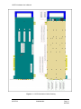
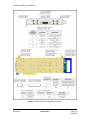
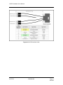
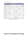
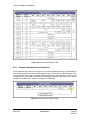
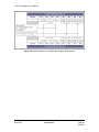
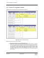
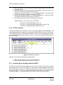
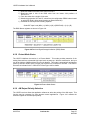
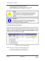
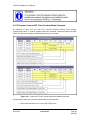
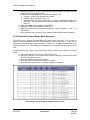
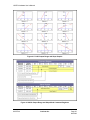
LS27P3 Hardware User’s Manual Dual channel Multi-Band RF Downconverter with AM Demodulation Document: Author: Date: Release: U027P301 B. Graber 08/16/09 Initial Lumistar Inc 5870 El Camino Real Carlsbad, California 92008 (760) 431-2181 www.lumi-star.com This document is the intellectual property of Lumistar Inc. The document contains proprietary and confidential information. Reproduction, disclosure, or distribution of this document is prohibited without the explicit written consent of Lumistar Inc. This document is provided as is, with no warranties of any kind. Lumistar Inc disclaims and excludes all other warranties and product liability, expressed or implied, including but not limited to any implied warranties of merchantability or fitness for a particular purpose or use, liability for negligence in manufacture or shipment of product, liability for injury to persons or property, or for any incidental, consequential, punitive or exemplary damages. In no event, will Lumistar Inc, be liable for any lost revenue or profits, or other indirect, incidental and consequential damages even if Lumistar Inc has been advised of such possibilities, as a result of this document or the usage of items described within. The entire liability of Lumistar Inc shall be limited to the amount paid for this document and its contents. RESTRICTED RIGHTS LEGEND Use, duplication, or disclosure by the Government is subject to restrictions set forth in subparagraph (c)(1)(ii) of the rights in Technical Data and Computer Software clause in DFARS 252.227-7013. Lumistar Inc and its logo are trademarks of Lumistar Inc. All other brand names and product names contained in this document are trademarks, registered trademarks, or trade names of their respective holders. © 2009 Lumistar Inc. All rights reserved. Lumistar Inc 5870 El Camino Real Carlsbad, CA 92008 (760) 431-2181 (760) 431-2665 Fax www.lumi-star.com LS27P3 Hardware User’s Manual TABLE OF CONTENTS 1 INTRODUCTION ...................................................................................................................... 4 1.2 2 MANUAL FORMAT AND CONVENTIONS ................................................................................... 4 THEORY OF OPERATION ...................................................................................................... 8 2.1 2.2 2.3 2.4 2.5 2.6 2.7 2.8 1ST DOWNCONVERSION ........................................................................................................ 8 1ST IF BAND-PASS FILTER..................................................................................................... 8 1ST LOCAL OSCILLATOR ........................................................................................................ 8 2ND DOWNCONVERSION ........................................................................................................ 9 2ND LOCAL OSCILLATOR ....................................................................................................... 9 2ND IF FILTER....................................................................................................................... 9 DIGITAL AGC/LIMITING AMPLIFICATION/AM DEMODULATION ................................................. 9 DIGITAL SIGNAL PROCESSING ENGINE (DSPE)..................................................................... 9 3 INSTALLATION AND CONFIGURATION ................................................................................. 10 3.1 3.2 3.3 3.4 4 PRODUCT OUTLINE DIAGRAMS ........................................................................................... 10 HARDWARE CONFIGURATION ............................................................................................. 10 PHYSICAL INSTALLATION .................................................................................................... 12 INTERCONNECTION ............................................................................................................ 13 PROGRAMMING ................................................................................................................... 16 4.1 BUS INTERFACES............................................................................................................... 16 4.2 COMMAND AND STATUS REGISTERS ................................................................................... 17 4.2.1 General Communications Interaction ...................................................................... 19 4.2.2 Hardware Identification ............................................................................................ 20 4.2.3 LED Control ............................................................................................................. 20 4.2.4 Read PROM Configuration Data Mode Command.................................................. 21 4.2.4.1 Hardware Port Configuration Register Contents.................................................. 23 4.2.5 Receiver RF Tuning Mode Command ..................................................................... 25 4.2.6 IF Filter Selection ..................................................................................................... 26 4.2.7 Received Signal Strength Indication (RSSI) ............................................................ 26 4.2.8 Protect Mode Status ................................................................................................ 27 4.2.9 AM Output Polarity Selection ................................................................................... 27 4.2.10 AM Index/Depth Status ............................................................................................ 28 4.2.11 AM Output Low-pass Filter Table Mode Command ................................................ 28 4.2.12 AM Frequency Counter............................................................................................ 30 4.2.13 AM Output Gain Controls......................................................................................... 31 4.2.14 AGC Time Constant Selection ................................................................................. 32 4.2.15 Program Custom AGC Time Constants Mode Command....................................... 33 4.2.16 Select AGC Output Range Mode Command ........................................................... 34 4.2.17 DAGC Control Mode Command .............................................................................. 36 4.2.18 DAGC Freeze .......................................................................................................... 36 4.2.19 IF Limited/ DAGC Output Select.............................................................................. 37 4.2.20 Pin J4-4/14 Control and Status................................................................................ 37 4.2.21 Read Configuration Switch Mode Command .......................................................... 39 4.2.22 Auto-Setup/Storage Function .................................................................................. 39 4.2.23 Internal/External Ref Select and PLL Status ........................................................... 40 4.2.24 Program External Reference Frequency Mode Command ..................................... 41 U027P301 Lumistar Inc. Page 3 08/16/09 LS27P3 Hardware User’s Manual 1 Introduction 1.1 General This document is the Hardware User’s Manual for the Lumistar LS27P3 Dual Channel Multi-band RF Downconverter. These products represent Lumistar’s 3rd generation of the LS27 Series of Dual Channel RF Downconverters. Figure 1-1 contains detailed model number construction. This document applies to all model combinations indicated by this figure. The intent of this document is to provide physical, functional, and operational information for the end user including hardware configuration, interconnection and software interfaces for the device. The design implements a Digital Signal Processor Engine (DSPE) controlled superhetrodyne downconverter with AM demodulation. In a single full-size PCI slot, the product provides two independent and autonomous multi-band downconversion stages. Each channel provides the conversion of up to four RF pass-bands to a 70MHz Intermediate Frequency (IF) output while providing AM demodulator of the input signal. The product’s standard configuration provides eight software selectable IF bandwidth filters, roughly placed at octave intervals, to reduce channel noise bandwidth and improve adjacent channel rejection. Table 1-1 provides specifications for electrical, mechanical, and operational characteristics of the LS27P3 product line. Figure 1-1 describes the product model number scheme. A block diagram of the product design is shown in Figure 1-2. 1.2 Manual Format and Conventions This manual contains the following sections: Chapter 1 provides a brief product overview and technical specifications Chapter 2 provides receiver theory of operation Chapter 3 provides installation and configuration instructions Chapter 4 provides programming information Throughout this document, several document flags will be utilized to emphasis warnings or other important data. These flags come in three different formats: Warnings, Cautions, and Information. Examples of these flags appear below. U027P301 Lumistar Inc. Page 4 08/16/09 LS27P3 Hardware User’s Manual Figure 1-1 LS27P3 Model Number Construction Details U027P301 Lumistar Inc. Page 5 08/16/09 LS27P3 Hardware User’s Manual Category: Mechanical Specifications: Details: Envelope Dimensions Form Factor Weight 12.35”(L) x 4.01”(W) x 0.62” (H) - PCI Full-length PCI ~ 24oz. Individual power requirements +3.3VDC @ 95mA +5VDC @ 3990mA +12VDC @ 30mA ~ 20 Watts Electrical Total Power (both Channels) Performance RF Tuner RF Input Bands Tuner Resolution Frequency Accuracy RF Input AGC Range Input Level without Damage Receiver Input P1dB Receiver Noise Figure 70MHz Phase Noise @ 100kHz Receiver OIP3 70MHz Output Level 2nd IF 3dB Bandwidths Available Demodulation 2185.5 - 2485.5 MHz (E-Band) 2200.5 - 2399.5 MHz (S-Band) 1710.5 - 1849.5 MHz (Upper L-Band) 1435.5 - 1539.5 MHz (Lower L-Band) 215.5 - 319.5 MHz (P-Band) Custom (Consult Factory) 50kHz (Typical) 0.002% (Max.) 0.001% (Typical) +10dBm to –100dBm +28dBm ( in “Protect mode”) +10dBm (typical) 5dB (typical @ threshold) Less than -110dBc (typical) > +15dBm (typical) -20dBm (+/- 1dBm) 250kHz, 500kHz, 1MHz, 2MHz, 5MHz, 10MHz, 20MHz, 40MHz Types AM -3dB Frequency Response AM Low-pass Filters AM -3dB Bandwidths AM Only 50kHz (AM Low-pass Bypass Mode) 32 Software Selectable External Reference Input/Output RF Signal Input IF Signal Output Accessory I/O Connector HD15 D-Style Connector Serial Interface Connectors (1) MMCX Jack (2) SMB Jack Receptacle (4) SMB Jack Receptacle (1) Molex 14-pin Connector (1) Discrete Connections (3) Molex 5-pin Connectors 50, 100, 200, 300, 400, 500, 600, 700, 800, 900, 1K, 1.1K, 1.2K, 1.3K, 1.4K, 1.5K, 1.6K, 1.7K, 1.8K, 1.9K, 2K, 3K, 4K, 5K, 6K, 7K, 8K, 9K, 10K, 15K, 20K, 50K Hz Connectors Environmental Temperature, Operational 0 to 70 C (Commercial) Temperature, Storage -20to 70 C Humidity, non-condensing <40 C 0-90%, >40 C 0-75% Table 1-1 Specifications for the LS27P3 U027P301 Lumistar Inc. Page 6 08/16/09 LS27P3 Hardware User’s Manual Figure 1-2 Block Diagram of LS27P3 Series Multi-band Channel U027P301 Lumistar Inc. Page 7 08/16/09 LS27P3 Hardware User’s Manual 2 Theory of Operation In order to more clearly understand the operation of the receiver, this section will detail the various stages of the receiver design. These stages are as follows: - 1st Downconversion 1st IF Band-pass Filter 1st Local Oscillator 2nd Downconversion 2nd Local Oscillator 2nd IF Filter Limiting Amplifier/AM Demodulation/Digital AGC (DAGC) Digital Signal Processing Engine (DSPE) With the exception of the DSPE, each of these sections are physically shielded and isolated from one another to facilitate the greatest EMI/RFI ingress and egress protection allowing the receiver exceptional performance. For the following sections, refer to the block diagram of Figure 1-2. 2.1 1st Downconversion The RF input is applied to the 1st Downconversion stage. The stage may optionally contain a bias-T which can be used to power an external LNA through the RF interface port. (Contact the factory for further details on this option.) A DAGC section is next in the signal chain for very high level signal protection and compression compensation. This is followed by a low-noise amplifier (LNA) to provide a large amount of gain while maintaining a very low noise figure enhancing the receiver’s overall sensitivity. Selectable RF band-pass filters follow the LNA. The RF signal is then mixed with the first local oscillator (LO) which converted to the 1st IF frequency. 2.2 1st IF Band-pass Filter The output of the 1st Downconversion stage is send through one of two1st IF filter paths based on the selection of high-side or low side conversion. To eliminate images and limit the overall noise bandwidth to the remaining receiver sections, a 50MHz band-pass filter is switched into the signal path. 2.3 1st Local Oscillator In a superhetrodyne design, local oscillators (LOs) are utilized to convert high frequencies to lower, “intermediate” frequencies. The first LO is injected into the mixer of the first Downconversion stage to accomplish this task. Mixers can either utilize a sum or difference frequency component to produce IF frequencies. For example, if an RF frequency of 2,200 MHz was to be converted to an intermediate frequency of 250MHz, a difference component of 1,950MHz could injected to the mixer or a sum frequency component of 2,450MHz could be applied. The difference component LO application is referred to a “low-side” conversion. The sum component application is referred to as “high-side” conversion. Both methods are equally valid and each has its own benefits. The LS27P3 design has the ability to utilize either approach and actually switch between the methods when necessary for performance reasons. U027P301 Lumistar Inc. Page 8 08/16/09 LS27P3 Hardware User’s Manual 2.4 2nd Downconversion The receiver designs contain a switchable 2nd Downconversion stage. Similar to the 1st Downconversion stage, it contains a mixer to convert the 1st IF frequency to a second IF frequency of 70MHz. If the RF frequency band is relatively low, as is the case for P-Band inputs, the on-board processor can bypass the 2nd Downconversion stage switching to a single superhetrodyne process. In either case, a low-pass filter is applied to the signal path at the output of this stage to reduce harmonics and low frequency noise from being applied to subsequent stages. 2.5 2nd Local Oscillator The second LO is injected into the mixer of the 2nd Downconversion stage to provide the second IF frequency of 70MHz. Like the first conversion stage, the second LO utilizes low-side injection for this conversion. A low-pass filter is applied to the LO output to minimize spurious and harmonic signals from being converted in the 2nd Downconversion stage. The 2nd LO is automatically disabled for RF bands that employ a single super heterodyne process. 2.6 2nd IF Filter From the output of the 2nd conversion stage, the resulting intermediate frequency is then applied to a group of bandpass filters to minimize noise bandwidth and improve adjacent channel rejection. The 2nd IF stage contains eight IF (SAW) filters centered at 70MHz and varying in bandwidth from 250kHz to 40MHz in approximately octave steps. 2.7 Digital AGC/Limiting Amplification/AM Demodulation Outputs from the 2nd IF Filter Stage are routed to the final signal detection, AM demodulation, and gain stage in the receiver. The output stage combines both a limiting amplifier and digital AGC (DACG) section. Included in the design is an AM demodulation stage for antenna tracking applications. The main system gain element provides for 90 to 110dB of signal gain. Signal level detection is utilized in DAGC controls. 2.8 Digital Signal Processing Engine (DSPE) The LS27P3 design contains a highly integrated digital signal processing engine (DSPE) which is utilized for linearization, filtering and control applications. This engine is composed of a digital signal processor, FPGA resources, ADCs, DACs and localized memory used to process the signal path parameters. Each of the channels is controlled and statused as an autonomous receiver. The engine performs “real-time” tasks as well as user software interfaces. U027P301 Lumistar Inc. Page 9 08/16/09 LS27P3 Hardware User’s Manual 3 Installation and Configuration Chapter 3 provides installation and configuration information. This chapter will locate serial numbers and product configuration information, familiarize the user with the layout of the board, and provide information on the proper installation and interconnection of the hardware. 3.1 Product Outline Diagrams Figure 3-1 contains an outline diagram of the top and bottom sides of the PCI versions of the product. Connector locations and switch positions are indicated. The model number, serial number, revision information and product options are denoted on the upper edge of the RF enclosure as indicated in the figure. 3.2 Hardware Configuration The receiver design contains configuration switches to control various functions. Figure 3-2 contains a diagram of the configuration switches along with the default factory positions for these switches. U027P301 Lumistar Inc. Page 10 08/16/09 LS27P3 Hardware User’s Manual Figure 3-1 LS27P3 Mechanical Outline Drawing U027P301 Lumistar Inc. Page 11 08/16/09 LS27P3 Hardware User’s Manual Figure 3-2 Receiver Configuration Switches 3.3 Physical Installation To install the receiver in the target computer system, the following procedure should be followed: 1. Perform a normal system shutdown of the PC system and remove the primary power plug. 2. Install the receiver in an unobstructed full-length PC slot ensuring that the receiver is properly seated in the interface bus socket. PCs vary in their mechanical configurations so it may be necessary to remove additional PC hardware to properly install the receiver. For PCI installations, it may be necessary to remove the blue ISA extension bracket at the rear of the PCI card, depending on the mechanical configuration of your particular platform. 3. Install a screw in the mounting panel to secure the unit. If the unit is installed in a portable or rack mount PC, it may also be necessary to secure the rear of the board to the chassis of the PC via standard self-locking cable ties. Some platforms also have a vertical hold down which can be adjusted to provide additional mechanical stability. U027P301 Lumistar Inc. Page 12 08/16/09 LS27P3 Hardware User’s Manual 3.4 Interconnection The receiver platforms provide multiple interface connectors. The interfaces are situated for internal and/or external cabling applications. Some of these physical configurations require special ordering instructions. (Consult the factory for further details.) Figure 3-3 provides interface pin-outs and mating connector information for all connectors. The LS27P3 receiver is shipped with a mating pigtail cable to interface with the HD15 mount plate connector. Figure 3-4 illustrates this cable pigtail. U027P301 Lumistar Inc. Page 13 08/16/09 LS27P3 Hardware User’s Manual Figure 3-3 LS27P3 Pin-outs and Mating Connectors U027P301 Lumistar Inc. Page 14 08/16/09 LS27P3 Hardware User’s Manual Figure 3-4 LS27P3 Interface Cable U027P301 Lumistar Inc. Page 15 08/16/09 LS27P3 Hardware User’s Manual 4 Programming This chapter provides receiver software interface and setup information. The receiver provides command and status interfaces through a 32-bit Peripheral Component Interface bus (PCI version 2.2). 4.1 Bus Interfaces The dual receiver interface is provided by an array of fourteen (14) command registers and sixteen (16) status registers mapped into the PC platform I/O space. No memory space mapping is required for interfacing with the unit. Each of the I/O registers is eight bits in length. PCI components do not have fixed address assignments. At system startup, a power-on routine scans the computer for PCI interfaces and assigns system resources to the devices found. Each PCI component is assigned an array of sixty-four 32-bit registers in what is referred to as configuration space. This area is normally not accessible anywhere in system address space and must be accessed by special means that are system-dependent. The following discussion applies to systems using MSDOS or Microsoft Windows platforms where PCI configuration space is accessed by BIOS calls. For the purposes of this document, these environments will be referred to as “typical” operating system environments. Other environments will have system-specific ways to access PCI configuration space. If you are utilizing non-Microsoft operating systems, consult your operating system documentation to determine PCI access methods. In addition, for environments that utilize processing platforms other than X86-type processors, Big/Little-Endian data format issues may also be present. To locate a receiver in a typical operating system environment, the following steps are required: 1.) Initialize an “index” value to zero. This index is allowed to be as large as 255 by the PCI specification. 2.) To locate the boards PCI9056 interface, set the machine registers as follows: AX = 0xB102 CX = 0x9056 DX = 0x10B5 SI = index 3.) Issue a software interrupt (0x1A). If the system returns from the interrupt with the carry flag set, any such devices are already located and no (more) exist. Exit the scanning routine. If the carry flag is clear, the BIOS call will have returned a “handle” in the BX register. U027P301 Lumistar Inc. Page 16 08/16/09 LS27P3 Hardware User’s Manual 4.) If the carry flag was clear, read the sub-identifier. Set the registers as follows: AX = 0xB10A BX = handle SI = 0x2C 5.) Issue another software interrupt (0x1A). The interrupt returns a value in the ECX register. If the value returned is 0x0273B00B, the handle points to a receiver and other configuration registers may be accessed. (Otherwise skip to step 7.) Set registers as follows: AX = 0xB10A BX = handle SI = 0x1C 6.) Issue another software interrupt (0x1A). Logically AND the value returned in the ECX register with 0x0FFF0. This yields the base I/O port of the receiver. Registers are in PCI I/O space and map simply as: Register Address = Base I/O Port + Register Address Offset 7.) Increment the index value and return to step 5. 4.2 Command and Status Registers Table 4-1 below contains the map for the LS27P3 command registers. Table 4-2 below contains the map for the LS27P3 status registers. Register address offsets are indicated in the tables for both of the independent receivers. More detailed discussions of the function and interaction of these registers will follow in subsequent sections. Discussions will follow a logical and functional flow rather than on a register-by-register method. All examples provided will be address receiver channel number 1 (RCVR1) and any general controls and status which apply to the overall product. Commands and status of receiver number 2 (RCVR2) are identical with the exception of offset address. U027P301 Lumistar Inc. Page 17 08/16/09 LS27P3 Hardware User’s Manual Table 4-1 Receiver Command Register Table U027P301 Lumistar Inc. Page 18 08/16/09 LS27P3 Hardware User’s Manual Table 4-2 Receiver Status Register Table 4.2.1 General Communications Interaction Communications with either of the receivers is via a command-response format. Commands sent from the host processor will cause a BUSY flag to be set in bit 0 of the DCxSTAT5 register. Once a command has been issued, application software should wait until the BUSY flag returns to a low state prior to issuing further commands or reading the requested status data. Each receiver contains its own BUSY flag. Figure 4-1 illustrates the BUSY flag. Figure 4-1 Receiver BUSY Flag Indication U027P301 Lumistar Inc. Page 19 08/16/09 LS27P3 Hardware User’s Manual 4.2.2 Hardware Identification The platform contains a single hardware identification register to provide software the ability to query the hardware to provide confidence that a receiver is physically present at the alleged address. This register is shown in Figure 4-2. Figure 4-2 Board Identification Register Successive reads from the GPSTAT1 register will return a string of ASCII characters in the lower 7 bit positions of the register as follows: Receiver Type:Hex Return String: LS27P3 0x4C, 0x53, 0x32, 0x37, 0x50, 0x33, 0x00 ASCII Return String: “L”, “S”, “2”, “7”, “P”, “3”, “NULL” This receiver presents these identification strings in a circular fashion terminating in a NULL character (0x00). Once the NULL character is received, subsequent reads from this register will recycle through the character string. 4.2.3 LED Control The rear of the receiver platform contains a bank of four Board ID LEDs. At initial application of power, the on-board DSPE assumes control of these indicators. The DSPE utilizes the LEDs to indicate power-up test and configuration memory load status. During the initial boot phase of operation (prior to operating system availability), all ID LEDs are all flashed on and off four times indicating that the primary DSPE functions have been successfully initialized. The internal control of these LEDs is complete in less than 3 seconds. Once the units internal processing and testing is complete, all LEDs are extinguished and control is returned to the host interface via bits 0 through 3 of GPCTRL2 register. Status of these LEDs can be read by the application software via bits 0 through 3 of GPSTAT2 register. Figure 4-3 illustrates registers used to command and status the boards LEDs. The LEDs are often used by the device driver or software application to provide receiver identification when multiple instances of a physical device are present in a system. U027P301 Lumistar Inc. Page 20 08/16/09 LS27P3 Hardware User’s Manual Figure 4-3 LED Control and Status 4.2.4 Read PROM Configuration Data Mode Command The unit provides the application software with hardware configuration information detailing options and capabilities. This factory configured data is held in non-volatile memory on the receiver in a configuration PROM. Each of the autonomous receivers can be configured uniquely so the design contains a separate configuration PROM for each receiver. The configuration PROM for receiver channel 1 (RCVR1) contains any common data that is shared between the two units and thus the arrangement of the second PROM will omit these common items. The contents of this configuration PROM are shown in Table 4-3. Registers required to access the PROM data are shown in Figure 4-4. U027P301 Lumistar Inc. Page 21 08/16/09 LS27P3 Hardware User’s Manual Table 4-3 Configuration PROM Contents U027P301 Lumistar Inc. Page 22 08/16/09 LS27P3 Hardware User’s Manual Figure 4-4 Configuration PROM Control and Status To access the configuration data, the following steps should be performed: 1.) Ensure that the BUSY flag is not set. (DCxSTAT5, bit 0) 2.) Place the receiver in PROM Read mode by setting the Mode Selection field of DCxCTRL5 as follows: 00010b 3.) Poll the BUSY flag until it returns low. 4.) In control register DCxCTRL6, write 01aaaaaab where the “aaaaaa“ field is the binary address offset of the configuration data to be read as shown in Table 4-3. 5.) Once the BUSY bit goes low, the lower byte of the requested configuration data will be available in DCxSTAT7, and the upper byte of data will reside in DCxSTAT8. 4.2.4.1 Hardware Port Configuration Register Contents The LS27P3 hardware can be configured with RF inputs and IF outputs in various locations. In many circumstances, the presence, routing and any selectable control of these ports needs to be identified to software applications. The configurations of these ports are strictly factory assembly dependent and thus are not software controllable. A configuration PROM register is present to indicate the positions and routing of these ports. These configuration definitions are described in detail in Figure 4-5 below. U027P301 Lumistar Inc. Page 23 08/16/09 LS27P3 Hardware User’s Manual Figure 4-5 PROM Hardware Port Configuration Register Bit Definitions U027P301 Lumistar Inc. Page 24 08/16/09 LS27P3 Hardware User’s Manual 4.2.5 Receiver RF Tuning Mode Command Registers that are required for RF tuning are depicted in Figure 4-6. Figure 4-6 Tuning Command Registers Band tuning should follow the process below: 1.) Ensure that the BUSY bit is not set. (DCxSTAT5, bit 0) 2.) Determine the valid RF tuning bands available for the receiver channel. To do this, examine the contents of the configuration PROM offsets 19 through 26 (See table 43). These PROM locations describe the upper and lower pass-band limits of each receiver band. No value outside of these bands will be tuned by the receivers DSPE so ensure that the tune value being requested by the user is valid. If the configuration PROM values are zero, this indicates that the RF band-pass filter has been omitted. U027P301 Lumistar Inc. Page 25 08/16/09 LS27P3 Hardware User’s Manual 3.) Place the receiver in RF Tune mode by setting the Mode Selection field DCxCTRL5 as follows: 00011b 4.) Divide the desired RF tuning frequency (Fc) by 256MHz, truncate the value to an integer and write the resulting value to DCxCTRL8. 5.) Perform the following calculation: (Fc modulo (256MHz))/1MHz. Truncate the value to an integer and write the resulting value to DCxCTRL7. 6.) Perform the following calculation: (Fc modulo (1MHz))/10kHz. Truncate the value to an integer and write the resulting value to DCxCTRL6. 7.) Once the BUSY flag goes low the tuning process is complete. Register Example: Tune the Receiver to 2252.5MHz DCxCTRL8 = 2252.5MHz/256MHz = 8.79 = 8 DCxCTRL7 = (2252.5MHz MOD 256MHz)/1MHz = 204.5 = 204 DCxCTRL6 = (2252.5MHz MOD 1MHz)/10kHz = 50 4.2.6 IF Filter Selection The receiver provides for the selection of one of up to eight 70MHz IF filter bandwidths. The available bandwidths are indicated in the configuration PROM locations 0 through 7 (See Table 43). If the PROM location for a particular filter contains a value of zero, this indicates that the filter is not installed and should not be selected. Figure 4-7 contains the register contents required to select the IF filters. Figure 4-7 70MHz Filter Selection Selection of the IF filter should follow the process below: 1.) Ensure that the BUSY bit is not set. (DCxSTAT5, bit 0) 2.) Enter the desired Signal Filter number in DCxCTRL2. 4.2.7 Received Signal Strength Indication (RSSI) DCxSTAT1 and DCxSTAT2 status registers provide a 12-bit indication of the RF signal strength being applied at the RF Input. This register is configured so as signal strength increases, the value of this register increases. To obtain the signal strength in dB, the value from the register must be applied to a first order polynomial equation whose factors are contained in the configuration PROM. To calculate the RSSI value in dBm, perform the following steps: U027P301 Lumistar Inc. Page 26 08/16/09 LS27P3 Hardware User’s Manual 1.) Read the 8LSBs of the RSSI value from DCxSTAT1 2.) Read the upper 4 bits of the RSSI value from the lowest 4-bit positions of DCxSTAT2. 3.) Form the values into a single 12-bit value. 4.) Obtain the polynomial “M” and “B” values from the configuration PROM values based on which RF Band is being tuned (starting at offsets 29 and 30). 5.) Calculate the results per the following equation: Scaled RF Input Level (dBm) = (0.0001) x (M) x (RSSI RAW) + (0.1) x (B) The RSSI Status registers are shown in Figure 4-8. Figure 4-8 Received Signal Strength Indication (RSSI) Status 4.2.8 Protect Mode Status The LS27P3 initializes the receiver in a “Protect Mode”. This mode provides protection of the analog front-end from unintended high input levels at power-up. With this mode active, the input can be as high as +28dBm without input circuit damage. This mode is automatically activated at power-up and will remain active until the first receiver tune command is received. The state of this mode is indicated in bit 7 of DCxSTAT2. See Figure 4-9 for details. Figure 4-9 Protect Mode Status 4.2.9 AM Output Polarity Selection The LS27P3 receiver allows the application software to select the polarity of the AM output. This function may be necessary for some antenna control applications. Figure 4-10 contains the selection register for the AM output polarity. U027P301 Lumistar Inc. Page 27 08/16/09 LS27P3 Hardware User’s Manual Figure 4-10 AM Output Polarity Selection Selection of the AM output polarity should follow the process below: 1.) Ensure that the BUSY bit is not set. (DCxSTAT5, bit 0) 2.) Enter the desired logic state in bit 7 of DCxCTRL4. 4.2.10 AM Index/Depth Status DCxSTAT3 contains the AM Index (or AM Depth) that has been detected in the post-processing of the AM demodulation. In AM modulation, 100% modulation is defined as the level where the negative peaks of the modulating signal reduce the transmitted signal output to zero. The LS27P3 measures this value and provides an AM Index depth estimate. The values returned indicate the percentage of AM modulation detected by the receiver. These values will vary from 0 to 100 and be held in the lower 6-bits of DCxSTAT3, which are direct percentage relations. It is important to note that AM Index detection is performed during all operational phases of the receiver. Detection of small amounts of AM that are a result of signal noise or other modulation formats is considered normal. Figure 4-11 illustrates the AM index Status register contents. Figure 4-11 AM Index Status 4.2.11 AM Output Low-pass Filter Table Mode Command The AM output of the LS27P3 allows the application software to add a low-pass filter to the AM output to filter the AM signal for the frequencies of interest. Thirty-two (32) AM low-pass filters are provided in the design. Since the configuration PROM page does not contain the -3dB corner frequency for the filters, these values are returned to the application software via a mode command. Figure 4-12 contains the registers associated with the AM output low-pass filter -3dB corner frequency table mode command. U027P301 Lumistar Inc. Page 28 08/16/09 LS27P3 Hardware User’s Manual Figure 4-12 AM Low-pass Output Filter Corner Frequency Mode Command The process of extracting the corner frequency table should follow the process below: 1.) Ensure that the BUSY bit is not set. (DCxSTAT5, bit 0) 2.) Place the receiver in AM Filter Table mode by setting the Mode Selection field in DCxCTRL5 as follows: 00110b 3.) Place the index value of the filter you wish to obtain the corner frequency for in DCxCTRL7 register (values between 0 and 31 are valid). 4.) Write any value to DCxCTRL6 to initiate the table read. 5.) Loop until the BUSY bit drops low. 6.) Read the 8 LSBs of the corner frequency in DCxSTAT7 and the 8 MSBs of the corner frequency in DCxSTAT8. The Index value will be written to DCxSTAT6. 7.) Repeat the steps above until all values have been read. U027P301 Lumistar Inc. Page 29 08/16/09 LS27P3 Hardware User’s Manual 4.2.12 AM Frequency Counter The receiver design provides the application software with an AM frequency counter via a mode command. Figure 4-13 contains register definitions associated with this function. Figure 4-13 AM Frequency Counter Mode Command Registers Access to the AM Frequency Counter should follow the process below: 1.) Ensure that the BUSY bit is not set. (DCxSTAT5, bit 0) 2.) Place the receiver in AM Frequency Counter mode by setting the Mode Selection field in DCxCTRL5 as follows: 00111b 3.) Write any value to DCxCTRL6 to initiate the Frequency Counter read process. 4.) Loop until the BUSY bit drops low. 5.) Read the 8 LSBs AM Frequency Counter from DCxSTAT6. 6.) Read the next 8 MSBs of the AM Frequency Counter from DCxSTAT7. 7.) Read the MSB from of the AM Frequency Counter from DCxSTAT8. U027P301 Lumistar Inc. Page 30 08/16/09 LS27P3 Hardware User’s Manual 4.2.13 AM Output Gain Controls The receiver provides the application software gain control of the AM output signal. This control is provided via a digital interface referred to in this documentation as a “Digipot”. The AM output gain control Digipot contains 100 steps of gain adjustment. The controls may be individually stepped in either direction or be programmed to a specific setting via the application software interface. The device does not provide feedback of the actual setting so the application software must keep track of the control setting. The AM output signal is factory configured for a 2Vp-p output (into a 50 ohm load) at an AM modulation depth of 50%. To increase the AM output voltage, the Digipot must be decremented in value. Conversely, to reduce the AM output voltage, increment the Digipot value. Figure 4-14 contains the command registers associated with the AM Output Gain controls. Figure 4-14 AM Gain Control Registers To individually step the AM Gain Digipot, follow this procedure: 1.) Ensure that the BUSY bit is not set. (DCxSTAT5, bit 0) 2.) Write a 0 to decrement the Digipot control or a 1 to increment the Digipot to the AM Gain Command in DCxCTRL3. 3.) Set the Update Bit in bit 7 of DCxCTRL3 to initialize the command. 4.) When the BUSY flag goes low, the Digipot action has completed. To program the AM Gain Digipot for a specified value, follow this procedure: 1.) Ensure that the BUSY bit is not set. (DCxSTAT5, bit 0) U027P301 Lumistar Inc. Page 31 08/16/09 LS27P3 Hardware User’s Manual 2.) 3.) 4.) 5.) Write a 2 to the AM Gain Command in DCxCTRL3. Write the desired value (0 to 99) to DCxCTRL7. Set the Update Bit in bit 7 of DCxCTRL3 to initialize the command. When the BUSY flag goes low, the Digipot action is complete. 4.2.14 AGC Time Constant Selection The first three bits of DC1xCTRL1 allow the application software to select an AGC Time Constant, which is applied to the DAGC Output and the discrete AGC Output signal. The time constants are related to the RSSI linearization processing that is being conducted via the DSP processor. As the time constant value is increased, the fundamental frequency of the DSP linearization process is decreased, thus reducing AM components in the RSSI output. Figure 415 contains the AGC time constant selection registers. Figure 4-15 AGC Time Constant Selection Selection of the AGC Time constant should follow the process below: 1.) Ensure that the BUSY bit is not set. (DCxSTAT5, bit 0) 2.) Enter the desired logic state in bits 0-3 of DCxCTRL1. U027P301 Lumistar Inc. Page 32 08/16/09 LS27P3 Hardware User’s Manual 4.2.15 Program Custom AGC Time Constants Mode Command As indicated in Figure 4-15, the AGC Time Constant Selection includes three customer programmable values. In order to program custom time constants, a mode command is provided. Figure 4-16 defines the registers associated with this mode command. Figure 4-16 Custom AGC Time Constant Programming Mode Command Programming Custom time constants should follow the process below: 1.) Ensure that the BUSY bit is not set. (DCxSTAT5, bit 0) U027P301 Lumistar Inc. Page 33 08/16/09 LS27P3 Hardware User’s Manual 2.) Place the receiver in Custom Time Constant mode by setting the Mode Selection field DCxCTRL5 as follows: 01010b 3.) Determine the value desired and calculate the multiplier value: a. Example: 5msecs is the desired time constant b. Multiplier Value = 5msec/0.1msec = 50 c. Boundary-check the value to determine if the value is between the ranges of 1 and 65535. 0 is an invalid number and will be treated by the DSPE firmware as a value of 1. 4.) Apply the 8 MSBs of the multiplier to DCxCTRL8. 5.) Apply the 8 LSBs of the multiplier to DCxCTRL7. 6.) Apply the time-constant assignment designator (values between 1 and 3) to DCxCTRL6. 7.) Once the BUSY flag goes low the time constant programming process is complete. 4.2.16 Select AGC Output Range Mode Command The LS27P3 has a software programmable AGC output range and slope. This is useful in antenna tracking applications that may require differing levels of AGC output. There are 12 independent AGC range/slope options as shown in Table 4-4. A graphic representation of the settings is in Figure 4-17. The settings are commanded via a mode selection as defined in Figure 4-18. Programming the AGC Output Slope and Range mode command should follow the process below: 1.) Ensure that the BUSY bit is not set. (DCxSTAT5, bit 0) 2.) Place the receiver in AGC Output Select mode by setting the Mode Selection field DCxCTRL5 as follows: 01011b 3.) Write the desired selection to DCxCTRL7. 4.) Write any value to DCxCTRL6 to initiate the change. 5.) Once the BUSY flag goes low, the selection process is complete. Table 4-4 AGC Output Range and Slope Selection Table U027P301 Lumistar Inc. Page 34 08/16/09 LS27P3 Hardware User’s Manual Figure 4-17 AGC Output Range and Slope Graphic Figure 4-18 AGC Output Range and Slope Mode Command Registers U027P301 Lumistar Inc. Page 35 08/16/09 LS27P3 Hardware User’s Manual 4.2.17 DAGC Control Mode Command The LS27P3 contains a digital AGC control which is controlled by the DSPE. Because of this digital control, there is an ability to provide various AGC “profiles” which respond differently based on the user’s desire. At present, there are two profiles that implemented: PROFILE_A, and LIMITED. Future profiles may be added to this list. PROFILE_A – allows essential no AGC controls over an >80dBm receiver range. In this mode when RF input signals are below -25dBm, the output varies directly with the input power. As the input goes up or down by 1dB, the IF output responds in the same manner. When the receiver is exposed to levels above -25dBm, attenuation will be added to the input in a linear dB fashion. LIMITED – allows the output level to be maintained at a constant level regardless of the input level. This DAGC mode takes full advantage of the AGC Time constant modes. The settings are commanded via a mode selection as defined in Figure 4-19. Programming the AGC Output Slope and Range mode command should follow the process below: 1.) Ensure that the BUSY bit is not set. (DCxSTAT5, bit 0) 2.) Place the receiver in DAGC Control mode by setting the Mode Selection field DCxCTRL5 as follows: 00011b 3.) Write the desired selection to DCxCTRL6. 4.) Once the BUSY flag goes low, the selection process is complete. Figure 4-19 DAGC Control Profile Mode Command Registers 4.2.18 DAGC Freeze The DAGC path of the LS27P3 has the ability to perform an AGC “Freeze” regardless of commanded profile. When commanded, this stops all AGC controls regardless the input condition. This can be very helpful during antenna calibration procedures. To command the DAGC freeze, follow the process below. Figure 4-20 contains the command register applicable selection bits: U027P301 Lumistar Inc. Page 36 08/16/09 LS27P3 Hardware User’s Manual 1.) Ensure that the BUSY bit is not set. (DCxSTAT5, bit 0) 2.) Write the desired selection to bit 3 of DCxCTRL1. 3.) Once the BUSY flag goes low, the selection process is complete Figure 4-20 AGC Freeze Flag 4.2.19 IF Limited/ DAGC Output Select The LS27P3 has the ability to provide two IF outputs. One of the outputs is a permanent “Hardware Limited” output which does not respond to DAGC profiles or the AGC FREEZE mode. The other is the DAGC output which is controllable. Of the two IF outputs provided, one is always a DAGC controlled output. The other is selectable between DAGC and the “Hardware Limited” mode. To select the switchable output state, a flag has been provided in the command register. To command this output, follow the procedure described below. command register applicable selection bits: Figure 4-21 contains the 1.) Ensure that the BUSY bit is not set. (DCxSTAT5, bit 0) 2.) Write the desired selection to bit 7 of DCxCTRL1. 3.) Once the BUSY flag goes low, the selection process is complete Figure 4-21 IF Limited Flag 4.2.20 Pin J4-4/14 Control and Status The LS27P3 contains a general purpose input/output discrete that is available from the J4 HD15 DSub connector. This signal is formatted in a manner that can be referred to as a low current “Biased Open/Ground” discrete. Figure 4-22 shows a diagram of the basic electrical interface signal arrangement. Figure 4-23 shows the control and status registers. U027P301 Lumistar Inc. Page 37 08/16/09 LS27P3 Hardware User’s Manual Figure 4-22 Pin J4-4/14 Electrical Interface Diagram Figure 4-23 Pin J4-4/14 Control and Status Registers Selection of the Accessory Output Controls should follow the process below: 1.) Ensure that the BUSY bit is not set. (DCxSTAT5, bit 0) 2.) Set bit 2 of DCxCTRL5 to command the output or read bit 2 of DCxSTAT5 as desired. U027P301 Lumistar Inc. Page 38 08/16/09 LS27P3 Hardware User’s Manual 4.2.21 Read Configuration Switch Mode Command The receiver has an auxiliary configuration switch that can be read by software. One of these switches is used by the on-board firmware and the other three are used for customer specialized software uses or future firmware options. Figure 3-2 shows the SW2 hardware switch. The SW2-1 switch location is used for the Auto-setup/Store functions. SW2-2, SW2-3, and SW2-4 are undefined at this time. Figure 4-24 shows the registers associated with the reading of this switch state. Figure 4-24 SW2 Status Update Mode Command/Status 4.2.22 Auto-Setup/Storage Function The receiver has the ability to store its presently programmed configuration and then automatically resume this state upon power-up. This function allows the receiver to be started without the necessity to initiate any control software, thus saving on start-up time. This function is initiated via switch SW2-1(See Figure 3-2). The parameters that are stored by this function are U027P301 Lumistar Inc. Page 39 08/16/09 LS27P3 Hardware User’s Manual displayed in Table 4-5. If SW2-1 is in the OFF position, the receiver DOES NOT retain any configuration data internally. SW2-1 applies to both receiver channels. Table 4-5 Auto-store Parameters 4.2.23 Internal/External Ref Select and PLL Status The LS27P3 design includes a flexible reference clock phase-locked loop distribution system. This system employs both an automated and application software controlled manual mode. At power-up, the clock distribution system monitors for the presence of an external reference at port J6 (see Figures 3-1 and 3-3). If there is no external reference present that matches the value in the configuration PROM (offset 53), the unit will automatically switch the J6 input port to an output mode, enable on on-board 10MHz TCXO (+/- 3ppm stability minimum), and the route the 10MHz TCXO source to both the J6 output (at 0 to -2dBm @ 50 ohms) and use it to synchronize the internal synthesizers. If the user wishes to take “Manual” control of the external reference source at some period after the unit has had power applied, the user can switch the internal TCXO off and reinitialize port J6 as a 50 ohm input to accept the external reference at input level of -2dBm to +15dBm. Once the user has taken “Manual” control of the external reference, the unit will remain in “Manual” mode until the next power cycle. At any time, the user can monitor whether the clock distribution network is synchronized. This can be done by monitoring bit 7 of GPSTAT2. The command and status registers used for the reference command and status are shown in Figure 4-25. U027P301 Lumistar Inc. Page 40 08/16/09 LS27P3 Hardware User’s Manual Figure 4-24 External/Internal Reference Select and Status Registers 4.2.24 Program External Reference Frequency Mode Command The LS27P3 allows the user to program the external reference frequency for values other than the default standard of 10MHz value. A total of four programmable values are allowed: 5MHz, 10MHz, 20MHz, and 25MHz. To program this value, a mode command is provided. The procedure for this programming is shown below. The registers used for this function are shown in Figure 4-25. 1.) Ensure that the BUSY bit is not set. (DCxSTAT5, bit 0) 2.) Place the receiver in Program External Reference mode by setting the Mode Selection field DCxCTRL5 as follows: 01000b 3.) Program the reference frequency in MHz in DCxCTRL7 (Valid values are 5, 10, 20, 25). 4.) Write any value to DCxCTRL6 to initiate the command. 5.) Once the BUSY flag goes low the time constant programming process is complete. U027P301 Lumistar Inc. Page 41 08/16/09 LS27P3 Hardware User’s Manual Figure 4-25 Program External Reference Frequency Mode Command/Status Registers U027P301 Lumistar Inc. Page 42 08/16/09