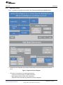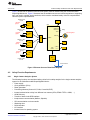
1
Safety Manual for VisionSurround28
Super/High/Mid Automotive Vision Applications
Processor
User's Guide
Literature Number: SPRUI16A
June 2015 – Revised October 2015
Contents
1
2
Scope ................................................................................................................................. 4
Introduction ......................................................................................................................... 5
2.1
Product Scope ............................................................................................................ 5
............................................................................................. 8
3
TI Standard DSP Development Process .................................................................................. 9
4
Product Safety Architecture and User Requirements ................................................................ 9
4.1
Safety Function Overview ............................................................................................... 9
4.2
Safety Function Requirements ........................................................................................ 13
4.3
Safety Mechanisms and Assumptions of Use ...................................................................... 20
5
Other System and Software Level Diagnostics ...................................................................... 40
6
Summary of Diagnostic Features ......................................................................................... 42
7
References ........................................................................................................................ 45
Appendix A Development Interface Agreement .............................................................................. 46
A.1
Appointment of Safety Managers ................................................................................... 46
A.2
Tailoring of the Safety Lifecycle ..................................................................................... 46
A.3
Activities Performed by TI ............................................................................................ 46
A.4
Information to be Exchanged ........................................................................................ 47
A.5
Parties Responsible for Safety Activities ........................................................................... 47
A.6
Supporting Processes and Tools .................................................................................... 47
A.7
Supplier Hazard and Risk Assessment............................................................................. 48
A.8
Creation of Functional Safety Concept ............................................................................. 48
Revision History .......................................................................................................................... 49
2.2
2
Product Safety Constraints
Table of Contents
SPRUI16A – June 2015 – Revised October 2015
Submit Documentation Feedback
Copyright © 2015, Texas Instruments Incorporated
www.ti.com
List of Figures
1
High-Level Device Diagram ................................................................................................ 7
2
TI Standard DSP QM Development Process
3
4
5
6
7
8
9
............................................................................ 9
Single Camera Analytics System Block Diagram ...................................................................... 11
Stereo Vision System Block Diagram ................................................................................... 12
Ethernet Surround View Block Diagram ................................................................................. 13
Block Diagram of Safety Functions for Single Camera Analytics System .......................................... 14
Block Diagram of Safety Functions for Stereo Camera Analytics System .......................................... 16
Block Diagram of Safety Functions for Ethernet Surround View System ........................................... 18
Operating States ........................................................................................................... 19
List of Tables
1
Spinlock States ............................................................................................................. 33
2
System With Software Level Diagnostics ............................................................................... 40
3
Activities Performed by TI vs Performed by Customer ................................................................ 46
4
Product Safety Documentation ........................................................................................... 47
5
Product Safety Documentation Tools and Formats .................................................................... 47
SPRUI16A – June 2015 – Revised October 2015
Submit Documentation Feedback
List of Figures
Copyright © 2015, Texas Instruments Incorporated
3
User's Guide
SPRUI16A – June 2015 – Revised October 2015
Safety Manual for VisionSurround28 Super/High/Mid
Automotive Vision Applications Processor
1
Scope
This safety manual for the VisionSurround28 Super/High/Mid device family products specifies the user's
responsibilities for installation and operation in order to maintain the desired safety level.
This document contains:
• Product scope:
– Purpose of product
– Intended application sectors
– Product safety constraints
• Information for each safety-related subsystem:
– Functions, interfaces and parameters of each safety-related subsystem
– Safety application overview
– Life time, environment and application limits
– Limits of application of each safety-related subsystem
– Device built-in safety logic
– User operation requirements to maintain the desired ASIL level, including a set of proof tests,
diagnostic tests and test interval
• A summary of the user’s responsibilities to integrate VisionSurround28 Super/High/Mid device family
products into safety system.
• Safety-related characteristics
• Terms and definitions
• Document revision status
The following information is documented in the FMEDA and is not repeated in this document. For
information on how to access the FMEDA, please contact your TI field representative.
• Summary of failure rates of the SoC estimated at the chip level
• Failure rates and diagnostic coverage for each sub-system
• Assumptions of use utilized in calculation of safety metrics
The user of this document should have a general understanding of the VisionSurround28 Super/High/Mid
device family products by having read the TDA2x ADAS Applications Processor 23mm Package (ABC
Package) Data Manual (SPRS859) and the TDA2x ADAS Applications Processor Silicon Revision 1.1
Technical Reference Manual (SPRUHK5).
OMAP is a trademark of Texas Instruments.
Cortex, ARM are registered trademarks of ARM Limited.
Arteris is a registered trademark of Arteris, Inc.
OMAP is a trademark of Texas Instruments.
Cortex, ARM are registered trademarks of ARM Limited.
Arteris is a registered trademark of Arteris, Inc.
4
Safety Manual for VisionSurround28 Super/High/Mid Automotive Vision
Applications Processor
Copyright © 2015, Texas Instruments Incorporated
SPRUI16A – June 2015 – Revised October 2015
Submit Documentation Feedback
Introduction
www.ti.com
2
Introduction
You, as a system and equipment manufacturer or designer, are responsible to ensure that your systems
(and any TI hardware or software components incorporated in your systems) meet all applicable safety,
regulatory and system-level performance requirements. All application and safety related information in
this document (including application descriptions, suggested safety measures, suggested TI products, and
other materials) is provided for reference only. You understand and agree that your use of TI components
in safety critical applications is entirely at your risk, and that you (as buyer) agree to defend, indemnify,
and hold harmless TI from any and all damages, claims, suits, or expense resulting from such use.
This safety manual provides information needed by system developers to assist in the creation of a safety
critical system using a VisionSurround28 Super/High/Mid device. TI does not claim any compliance to any
industry safety standard or Automotive Safety Integrity Level (ASIL). The devices of this family are
targeted to support systems which are QM and ASIL A. The Safety Manual specifies the user's
responsibilities for installation and operation in order to maintain the desired safety level.
The following information is documented in the Detailed Safety Analysis Report for VisionSurround28
Super/High/Mid device and is not repeated in this document:
• Fault model used to estimate device failure rates suitable to enable calculation of customized failure
rates
• Quantitative FMEA (also known as Failure Modes, Effects, and Diagnostics Analysis (FMEDA)) with
detail to the submodule level of the device, suitable to enable calculation based on customized
application of diagnostics
The user of this document should have a general familiarity with the VisionSurround28 Super/High/Mid
device. This document is intended to be used in conjunction with the device-specific data sheets, technical
reference manuals, and other documentation for the products under development.
For more information regarding the Safety Report, contact your TI sales representative.
2.1
2.1.1
Product Scope
Purpose of the Product
The purpose of the VisionSurround28 Super/High/Mid device is to function as a digital signal processor
(DSP) in embedded automotive applications in the driver assistance space. Some of these applications
may be safety critical.
Multiple safety applications were analyzed during concept and design phase for this product in order to
support Safety Element Out Of Context (SEooC) development according to ISO26262-10:2011. The
product originally was not developed per ISO26262 standard process and hence qualifies as QM. At the
same time, deliveries are made to customers to enable item (system) level safety analysis. These
deliveries include the safety manual, the safety analysis reports and FMEDAs. No assumptions have been
made in the safety analysis reports for whether a particular item will utilize a block of VisionSurround 28
Super/High/Mid or not. The report includes the failure rates for all the blocks without making any
assumptions on the usage of that particular block for a given system. It is customer’s responsibility to
utilize the reports provided in context of their own usage and system requirements.
The VisionSurround28 Super/High/Mid device was not developed according to any existing safety
standard and no compliance to these standards is claimed.
2.1.2
Application Sectors
The VisionSurround28 Super/High/Mid device is intended to be usable in automotive Advanced Driver
Assistance Systems. Specific targeted application segments include, but are not limited to:
• Front Camera
– Land Departure Warning
– Traffic Sign Recognition
– High Beam Assist
– Collision Mitigation
SPRUI16A – June 2015 – Revised October 2015
Submit Documentation Feedback
Safety Manual for VisionSurround28 Super/High/Mid Automotive Vision
Applications Processor
Copyright © 2015, Texas Instruments Incorporated
5
Introduction
•
•
•
www.ti.com
Backup Camera
– Obstacle Detection
– Park Assist
Surround View Systems
– Ethernet Surround View
– LVDS Surround View
Radar
– Long Range Radar
– Short Range Radar
As this device is a general market rather than custom or bespoke product, it cannot be said that a specific
implementation configuration can be assumed. As long as the requirements specified in this document are
followed, the DSP can also be used in safety critical applications beyond the ones mentioned above.
6
Safety Manual for VisionSurround28 Super/High/Mid Automotive Vision
Applications Processor
Copyright © 2015, Texas Instruments Incorporated
SPRUI16A – June 2015 – Revised October 2015
Submit Documentation Feedback
Introduction
www.ti.com
2.1.3
Application Sectors
Figure 1 provides a very high-level overview of the VisionSurround28 Super/High/Mid device.
A
To identify the correct configuration for the module in the block diagram, see the device-specific technical reference
manual.
Figure 1. High-Level Device Diagram
•
The device is composed of the following subsystems:
– Cortex®-A15 microprocessor unit (MPU) subsystem
– Digital signal processor (DSP) C66x subsystems
– Image and video accelerator high-definition (IVA-HD) subsystem
SPRUI16A – June 2015 – Revised October 2015
Submit Documentation Feedback
Safety Manual for VisionSurround28 Super/High/Mid Automotive Vision
Applications Processor
Copyright © 2015, Texas Instruments Incorporated
7
Introduction
•
•
www.ti.com
– Cortex-M4 image processing unit (IPU) subsystem, including two ARM® Cortex-M4
microprocessors
– Embedded vision engine (EVE) subsystems
– Programmable real-time unit (PRU) subsystem
– Display subsystem (DSS)
– Video input capture (VIP)
– 3D-graphics processing unit (GPU) subsystem, including POWERVR SGX544 dual-core
– Debug subsystem
The device provides a rich set of connectivity peripherals, including among others:
– PCI Express Gen2 subsystem
– Gigabit Ethernet (GMAC) subsystem
– DCAN subsystems
The device also integrates:
– On-chip memory
– External memory interfaces (EMIF)
– Memory management
– Level 3 (L3) and level 4 (L4) interconnects
– Real-time clock (RTC)
– General-purpose (GP) timers
– Watchdog timer (WDT)
– Interprocessor communication (Spinlocks, Mailboxes)
– Multichannel audio serial port (McASP)
– Serial peripheral interfaces (SPI)
– Inter-integrated circuit (I2C) interfaces
– Universal asynchronous receiver/transmitter (UART) modules
– General-purpose input/output (GPIO)
– System and serial control peripherals
The ADAS VisionSurround28 Super/High/Mid device is a high-performance, automotive vision application
device based on enhanced OMAP™ architecture integrated on a 28-nm technology.
2.2
Product Safety Constraints
The VisionSurround28 Super/High/Mid device is not designed to meet any existing (IEC61508, ISO26262)
or future safety standards. If the device is used in the context of functional safety, it has to be treated as a
Quality Managed (QM) device.
Multiple safety applications were analyzed during concept and design phase for this product in order to
support SEooC development according to ISO26262-10:2011. The product originally was not developed
per ISO26262 standard process and qualifies as QM. At the same time, deliveries are made to customers
to enable item (system) level safety analysis. These deliveries include the safety manual, the safety
analysis reports and FMEDAs. No assumptions have been made in the safety analysis reports as to
whether a particular item utilizes a block of VisionSurround 28 Super/High/Mid or not. The report includes
the failure rates for all the blocks without making any assumptions on the usage of that particular block for
a given system. It is the customer’s responsibility to utilize the reports provided in context of their own
usage and system requirements.
Since the VisionSurround 28 Super/High/Mid silicon is targeted for a variety of safety applications, there is
no fixed FTTI that TI as a supplier could propose. It is the responsibility of the customer to utilize the
methods and safety features outlined in the device-specific safety manual and technical reference manual
to meet their own identified FTTI requirements.
8
Safety Manual for VisionSurround28 Super/High/Mid Automotive Vision
Applications Processor
Copyright © 2015, Texas Instruments Incorporated
SPRUI16A – June 2015 – Revised October 2015
Submit Documentation Feedback
TI Standard DSP Development Process
www.ti.com
3
TI Standard DSP Development Process
Texas Instruments has been developing products for the automotive applications for over twenty years.
Automotive markets have strong requirements on quality management and high reliability of product.
Though not explicitly developed for compliance to a functional safety standard, the TI standard DSP
development process already features many elements necessary to manage systematic faults. This
development process can be considered to be Quality Managed (QM), but does not achieve an IEC 61058
Safety Integrity Level (SIL) or ISO 26262 Automotive Safety Integrity Level (ASIL).
The standard process breaks development into phases:
• Concept
• Commissioning
• Create
• Validation
• Ramp
The standard development process is illustrated in Figure 2.
Concept
Commissioning
Marketing
System Team
Identify new
product
opportunities
Architectural
Requirements
Validate
Create
Ramp or
Sustain
Cross Functional Team
System
Requirements
IC design
and layout
Bench ATE
Validation
Inventory
Buildup
Product Plan
Develop
manufacturing
Qualification
Optimize Test
Flow and Yield
Product
Requirements
Qualification
Plan
Develop and Build marketing
Collateral
Project Risks Assessment
Figure 2. TI Standard DSP QM Development Process
4
Product Safety Architecture and User Requirements
4.1
Safety Function Overview
4.1.1
Environment and Lifetime Limits
4.1.1.1
Service Life
A useful lifetime, based on experience, should be assumed. The failure rate stated in the FMEDA only
applies within the useful lifetime of the component. Beyond the useful lifetime, the result of the
probabilistic calculation method is meaningless, as the probability of failure significantly increases with
time. The useful lifetime is highly dependent on the subsystem itself and its operating conditions.
This assumption of a constant failure rate is based on the bathtub curve.
SPRUI16A – June 2015 – Revised October 2015
Submit Documentation Feedback
Safety Manual for VisionSurround28 Super/High/Mid Automotive Vision
Applications Processor
Copyright © 2015, Texas Instruments Incorporated
9
Product Safety Architecture and User Requirements
www.ti.com
The VisionSurround28 Super/High/Mid does not have any significant factors that are known to limit the
useful lifetime. A 10 year useful lifetime can be assumed as a conservative measure. It is the responsibility
of the manufacturer of a safety product utilizing the VisionSurround28 Super/High/Mid to determine any
useful lifetime limitations of other components used in the product design and disclose them in their
device-specific FMEDA and user manual.
When actual experience indicates a shorter useful lifetime than indicated in this section, the number based
on actual experience should be used.
4.1.1.2
Electrical Specifications and Environment Limits
The Recommended Operating Conditions section in the TDA2x ADAS Applications Processor 23mm
Package (ABC Package) Data Manual (SPRS859) and the PRCM Subsystem Environment section in the
TDA2x ADAS Applications Processor Silicon Revision 1.1 Technical Reference Manual (SPRUHK5)
specify the environmental conditions.
The user should ensure these constraints are kept. Only the Q version device should be considered in the
Automobile industry.
4.1.1.3
Mechanical Environment Constraints
The constraints on mechanical, humidity, and temperature in the reflow oven are stated in AEC-Q100 Rev
G. The user should ensure these constraints are kept.
4.1.1.4
Operating Frequency Limits
The Operating Performance Points section in the TDA2x ADAS Applications Processor 23mm Package
(ABC Package) Data Manual (SPRS859) specifies the operating performance point for processor clocks
and device core clocks. The user should ensure these constraints are kept.
4.1.1.5
•
•
10
Other Foreseeable Environment Disturbances
Radiation
All the soft error rate (SER) calculations in the FMEDA are based on NYC sea level cosmic particles
and ultra-low alpha emission package. The soft error caused by the cosmic particles needs to be
reevaluated if this product applies to a higher altitude. For more details on failure rates at higher
altitudes if necessary for your product safety analysis, contact your TI sales representative. This
product is not allowed to be used in outer space safety applications. Failures due to protons and other
heavy nuclei need to be considered in outer space. All TI failure rates driven by alpha particles are
based upon the usage of ultra-low alpha mold compound in packaging (<0.002 alpha/(cm2hr)).
EM Immunity
The ESD tolerance of this product is documented in the Absolute Maximum Ratings section of the
TDA2x ADAS Applications Processor 23mm Package (ABC Package) Data Manual (SPRS859). Any
ESD event higher than this limit may cause a permanent damage to the IC. The user is responsible to
implement measures to prevent ESD events higher than the ESD tolerance limit. This product should
not be exposed under any high frequency (>1 MHz) electric field larger than 400V/m or any magnetic
field larger than 1.07A/m. Exposition to such a field may cause communication interrupt, soft error,
hard error (can be recovered by a power cycle) or permanent damage to the IC. The user is
responsible to implement shielding, grounding, filtering or other methods to ensure the electromagnetic
field strength is under the limits mentioned above.
Safety Manual for VisionSurround28 Super/High/Mid Automotive Vision
Applications Processor
Copyright © 2015, Texas Instruments Incorporated
SPRUI16A – June 2015 – Revised October 2015
Submit Documentation Feedback
Product Safety Architecture and User Requirements
www.ti.com
4.1.2
Safety Application Overview
The VisionSurround28 Super/High/Mid device is intended to be used in a number of safety critical
automotive applications, for example, a single camera analytics system, a stereo camera analytics
system, a surround view system, and so forth.
Figure 3 shows how a single camera analytics system could be realized using the VisionSurround28
Super/High/Mid device. Figure 3 illustrates how the available sensors and varied integrations of supporting
logic can result in multiple device interfaces, which must be considered safety critical to comprehend all
common system implementations.
DDR
FLASH
PRU
FPGA
Debug
QSPI,
GPMC
STM trace
DSP trace
JTAG
CMOS Sensors
VideoOut
I2C
16 bit/sample
25/27MHz
TBD - TDA1MSA/SV
Video In
EMAC
GPIO
Power
Supply
CLK_OUT
SPI,
UART
RESET_OUT
1280x800
@30fps
CAN
Flashing and
Debugging
Local CAN bus
DSP
PCIe
PCIe
DDR
MCU
ADC
CAN1
CAN0
CLK and
RST
MON.
Vehicle CAN bus
OPTIONAL
Figure 3. Single Camera Analytics System Block Diagram
SPRUI16A – June 2015 – Revised October 2015
Submit Documentation Feedback
Safety Manual for VisionSurround28 Super/High/Mid Automotive Vision
Applications Processor
Copyright © 2015, Texas Instruments Incorporated
11
Product Safety Architecture and User Requirements
www.ti.com
Figure 4 shows how a stereo camera analytics system could be realized using the VisionSurround28
Super/High/Mid device. Figure 4 illustrates how the available sensors and varied integrations of supporting
logic can result in multiple device interfaces, which must be considered safety critical to comprehend all
common system implementations.
DDR
FLASH
ECD
bits
DSP
(Q)SPI,
GPMC
Debug
25/27MHz
STM trace
DSP trace
CMOS Sensors
I2C
VideoOut
16 bit/sample
Video In
I2C
EMAC
16 bit/sample
Video In
Power
CLK_OUT
GPIO
RESET_OUT
SPI,
UART
Only for
Development
CAN
Local CAN bus
DSP
PCIe
PCIe
DDR
MCU
ADC
CAN1
CAN0
CLK and
RS
Vehicle CAN bus
Figure 4. Stereo Vision System Block Diagram
12
Safety Manual for VisionSurround28 Super/High/Mid Automotive Vision
Applications Processor
Copyright © 2015, Texas Instruments Incorporated
SPRUI16A – June 2015 – Revised October 2015
Submit Documentation Feedback
Product Safety Architecture and User Requirements
www.ti.com
Figure 5 shows how an ethernet surround view system could be realized using the VisionSurround28
Super/High/Mid device. Figure 5 illustrates how the available sensors and varied integrations of supporting
logic can result in multiple device interfaces, which must be considered safety critical to comprehend all
common system implementations.
MJPEG/ H.264
Encode
1280x800
@30fps
DDR2
I2C
EMAC
DSP
Video In
STM trace
DSP trace
JTAG
MJPEG / H.264
Encode
1280x800
@30fps
2
I C
1024x768 @60fps
EMAC
Video In
VideoOut
E- Net
Switch
MJPEG / H.264
Encode
1280x800
@30fps
Debug
G- EMAC
I2C
27MHz
EMAC
Video In
MJPEG / H.264
Encode
1280x800
@30fps
SPI/
UART
(Q)SPI /
GPMC
FLASH
I2C
EMAC
Video In
MCU
MJPEG/ H.264
Encode
CAN0
Vehicle CAN bus
Figure 5. Ethernet Surround View Block Diagram
4.2
4.2.1
Safety Function Requirements
Single Camera Analytics System
The following functions are considered safety critical in this safety analysis for the single camera analytics
system for the VisionSurround28 Super/High/Mid device:
• Power supply
• Clock generation (PLLs)
• Reset generation
• Processing elements (Cortex-A15, C66x, Cortex-M4, EVE)
• Internal read and write activity from different bus masters (CPUs, EDMA TPTCs + MMU, …)
• OCMC Memory
• Transfer of data via the DDR interface
• Interprocessor communication (Mailbox, Spinlock)
• SPI communication to microcontroller
• Watchdog timer
• DCAN interface
• I2C interface
• Internal timers for operating system
SPRUI16A – June 2015 – Revised October 2015
Submit Documentation Feedback
Safety Manual for VisionSurround28 Super/High/Mid Automotive Vision
Applications Processor
Copyright © 2015, Texas Instruments Incorporated
13
Product Safety Architecture and User Requirements
www.ti.com
Figure 6 shows the device block diagram with the safety functions for the single camera analytics system
mapped to it. The red rectangles denote the blocks on which safety functions need to be mapped.
Figure 6. Block Diagram of Safety Functions for Single Camera Analytics System
14
Safety Manual for VisionSurround28 Super/High/Mid Automotive Vision
Applications Processor
Copyright © 2015, Texas Instruments Incorporated
SPRUI16A – June 2015 – Revised October 2015
Submit Documentation Feedback
Product Safety Architecture and User Requirements
www.ti.com
4.2.2
Stereo Camera Analytics System
In general, the following functions are considered safety critical in this safety analysis for the single
camera analytics system for the VisionSurround28 Super/High/Mid device:
• Power supply
• Clock generation (PLLs)
• Reset generation
• Processing elements (Cortex-A15, C66x, Cortex-M4, EVE)
• Internal read and write activity from different bus masters (CPUs, EDMA TPTCs + MMU, …)
• OCMC memory
• Transfer of data via the DDR interface
• Interprocessor communication (Mailbox, Spinlock)
• SPI communication to microcontroller
• Watchdog timer
• DCAN interface
• I2C interface
• Internal timers for operating system
• Display subsystem (DSS)
SPRUI16A – June 2015 – Revised October 2015
Submit Documentation Feedback
Safety Manual for VisionSurround28 Super/High/Mid Automotive Vision
Applications Processor
Copyright © 2015, Texas Instruments Incorporated
15
Product Safety Architecture and User Requirements
www.ti.com
Figure 7 shows the device block diagram with the safety functions for the stereo camera analytics system
mapped to it. The red rectangles denote the blocks on which safety functions need to be mapped.
Figure 7. Block Diagram of Safety Functions for Stereo Camera Analytics System
16
Safety Manual for VisionSurround28 Super/High/Mid Automotive Vision
Applications Processor
Copyright © 2015, Texas Instruments Incorporated
SPRUI16A – June 2015 – Revised October 2015
Submit Documentation Feedback
Product Safety Architecture and User Requirements
www.ti.com
4.2.3
Ethernet Surround View System
In general, the following functions are considered safety critical in this safety analysis for the single
camera analytics system for the VisionSurround28 Super/High/Mid device:
• Power supply
• Clock generation (PLLs)
• Reset generation
• Processing elements (Cortex-A15, C66x, Cortex-M4, EVE)
• Internal read and write activity from different bus masters (CPUs, EDMA TPTCs + MMU, …)
• OCMC memory
• Transfer of data via the DDR interface
• Interprocessor communication (Mailbox, Spinlock)
• SPI communication to microcontroller
• Watchdog timer
• DCAN interface
• I2C interface
• Internal timers for operating system
• GMAC
• Display subsystem (DSS)
• IVA subsystem
• GPU
• UART
SPRUI16A – June 2015 – Revised October 2015
Submit Documentation Feedback
Safety Manual for VisionSurround28 Super/High/Mid Automotive Vision
Applications Processor
Copyright © 2015, Texas Instruments Incorporated
17
Product Safety Architecture and User Requirements
www.ti.com
Figure 8 shows the device block diagram with the safety functions for the Ethernet surround view system
mapped to it. The red rectangles denote the blocks on which safety functions need to be mapped.
Figure 8. Block Diagram of Safety Functions for Ethernet Surround View System
18
Safety Manual for VisionSurround28 Super/High/Mid Automotive Vision
Applications Processor
Copyright © 2015, Texas Instruments Incorporated
SPRUI16A – June 2015 – Revised October 2015
Submit Documentation Feedback
Product Safety Architecture and User Requirements
www.ti.com
4.2.4
Operating States
The VisionSurround28 Super/High/Mid device products have a common architectural definition of
operating states. These operating states should be observed by the system developer in their software
and system level design concepts. The operating states state machine is show in Figure 9 and described
below.
Power applied
nPOR held
nPOR released
Powered Off
Safe
Power Removed
Cold Boot
nPOR driven
nRESET released internally
nPOR driven
Warm Boot
nPOR driven
SYS_nRESET driven
Proof tests completed
System init completed
Operational
Figure 9. Operating States
•
•
•
•
•
Powered Off - This is the initial operating state of the VisionSurround28 Super/High/Mid device. No
power is applied to the different power supply rails and the device is non-functional. This state can only
transition to the safe state, and can only be reached from the safe state.
Safe - In the safe state, the VisionSurround28 Super/High/Mid device is powered but non-operational.
The nPOR (power-on reset, also known as cold reset) is asserted by the system but is not released
until power supplies have ramped to a stable state. When the product is in the safe state, the CPU and
peripherals are nonfunctional. The Terminal Description section in the TDA2x ADAS Applications
Processor 23mm Package (ABC Package) Data Manual (SPRS859) provides details about the pin
behavior during reset.
Cold Boot - In the cold boot state, key analog elements, digital control logic, and debug logic are
initialized for future use. The CPU remains powered but non-operational. When the cold boot process
is completed, the nRESET signal is internally released, leading to the warm boot stage. The nRESET
signal transition change can be monitored externally on the nRSTOUT output pin.
Warm Boot - The warm boot mode resets digital logic and enables the Cortex-A15. The Cortex-A15
begins executing software from the internal boot ROM and software initialization of the device begins.
There is no hardware interlock to say that warm boot is completed; this is a software decision.
Operational - During the operational mode, the device is capable of supporting safety critical
functionality.
SPRUI16A – June 2015 – Revised October 2015
Submit Documentation Feedback
Safety Manual for VisionSurround28 Super/High/Mid Automotive Vision
Applications Processor
Copyright © 2015, Texas Instruments Incorporated
19
Product Safety Architecture and User Requirements
4.2.5
www.ti.com
Management of Errors
The error response is an action that is taken by the VisionSurround28 Super/High/Mid device or system
when an error is indicated. There are multiple potential error responses possible for the VisionSurround28
Super/High/Mid product family. The system integrator is responsible to determine what error response
should be taken and to ensure that this is consistent with the system safety concept.
• CPU abort - This response is implemented directly in the CPU, for diagnostics implemented in the
CPU. During an abort, the program sequence transfers context to an abort handler and software has
an opportunity to manage the fault.
• CPU interrupts - This response can be implemented for diagnostics outside of the CPU. An interrupt
allows events external to the CPU to generate a program sequence context transfer to an interrupt
handler where software has an opportunity to manage the fault.
• Generation of warm reset - This response allows the device to change states to warm boot from
operational state. The warm reset could be generated from an external monitor on nRESET or
internally by the software global warm reset, emulation warm reset, or watchdog. Re-entry to the warm
reset state allows possibility for software recovery when recovery in the operational state was not
possible.
• Generation of cold reset - This response allows the device to change state to safe state from cold boot,
warm boot, or operational states. From this state, it is possible to re-enter cold boot to attempt recovery
when recovery via warm boot is not possible. It is also possible to move to the powered-down state, if
desired, to implement a system level safe state. This response can be generated by the software
global cold reset or nPOR pin, but is primarily driven by monitors external to the VisionSurround28
Super/High/Mid device.
4.3
Safety Mechanisms and Assumptions of Use
You, as a system and equipment manufacturer or designer, are responsible to ensure that your systems
(and any TI hardware or software components incorporated in your systems) meet all applicable safety,
regulatory and system-level performance requirements. All application and safety related information in
this document (including application descriptions, suggested safety measures, suggested TI products, and
other materials) is provided for reference only. You understand and agree that your use of TI components
in safety critical applications is entirely at your risk, and that you (as buyer) agree to defend, indemnify,
and hold TI harmless from any and all damages, claims, suits, or expense resulting from such use.
In this section, the safety mechanisms for each major functional block of the VisionSurround28
Super/High/Mid device architecture are summarized and general assumptions of use are provided. This
information should be used to determine the strategy for utilizing safety mechanisms. The details of each
safety mechanism can be found in the device-specific technical reference manual for the
VisionSurround28 Super/High/Mid device used.
There are many diverse ways to implement safe systems and alternate safety mechanisms may be
possible that can provide support to achieve desired safety metrics. The categories of recommendation
are as follows:
• Mandatory - A mandatory notation indicates a safety mechanism that is always operable during normal
functional operation and cannot be disabled by user action.
• Highly Recommended - A highly recommended notation indicates a safety mechanism that TI believes
to provide a high value of diagnostics that are difficult to implement by other means. The user retains
the choice whether or not to utilize the safety mechanism in their design, as user action is either
needed to enable the safety mechanism or user action can disable the safety mechanism.
• Recommended - A recommended notation indicates a safety mechanism that TI believes to provide a
valuable diagnostic that can also be implemented by other means. The user retains the choice whether
or not to utilize the safety mechanism in their design, as user action is either needed to enable the
safety mechanism or user action can disable the safety mechanism.
• Optional - An optional notation indicates a safety mechanism that TI believe to provide a lower value
diagnostic that can also be implemented by other means. The user retains the choice whether or not to
utilize the safety mechanism in their design, as user action is either needed to enable the safety
mechanism or user action can disable the safety mechanism.
20
Safety Manual for VisionSurround28 Super/High/Mid Automotive Vision
Applications Processor
Copyright © 2015, Texas Instruments Incorporated
SPRUI16A – June 2015 – Revised October 2015
Submit Documentation Feedback
Product Safety Architecture and User Requirements
www.ti.com
Depending on the safety standard and end equipment targeted, it may be necessary to manage not only
single point faults, but also latent faults. Per ISO 26262:2011, the latent faults to be considered are when
the faults in a function are both present: the capability to violate a safety goal and to cause a fault in the
safety mechanism. Latent fault testing does not need to occur during the fault tolerant time interval, but
can be performed at boot time, at shut down, or periodically as determined by the system developer. Many
of the safety mechanisms described in this section can be used as primary diagnostics, diagnostics for
latent fault, or both. When considering system design for management of latent faults, take care to include
failure of CPU and memories in consideration for any primary diagnostic that is executed via software.
4.3.1
Power Supply
The VisionSurround28 Super/High/Mid device family products require an external device to supply the
necessary voltages and currents for proper operation. Separate voltage rails are available for core logic,
I/O, phase-locked loop (PLL) and other functions.
4.3.1.1
External Voltage Supervisor
It is highly recommended to use an external voltage supervisor to monitor all voltage rails. The voltage
supervisor should be configured with overvoltage and undervoltage thresholds matching the voltage
ranges supported by the target device (as noted in the device-specific data sheet). Error response,
diagnostic testability and any necessary software requirements are defined by the external voltage
supervisor selected by the system integrator.
4.3.1.2
Power Sequencing
In order for the VisionSurround28 Super/High/Mid device to function properly, it is highly recommended to
implement the power sequencing requirements as outlined in the Power Sequence section of the TDA2x
ADAS Applications Processor 23mm Package (ABC Package) Data Manual (SPRS859).
4.3.1.3
•
•
•
4.3.2
Notes
VisionSurround28 Super/High/Mid management of voltage supervision at system level can be
simplified by using a TI system basis chip, developed for use with the family.
Devices can be implemented with multiple power rails that are intended to be ganged together on the
system PCB. For proper operation of power diagnostics, it is recommended to implement one voltage
supervisor per ganged rail.
Common mode failure analysis of the external voltage supervisor may be useful to determine
dependencies in the voltage generation and supervision circuitry.
Power Management
The power, reset and clock module (PRCM) is responsible for control of switchable power domains.
Dependent on the family variant used, one or more power domains can be implemented. Power domains
can be permanently configured at manufacturing time by TI or they can be user programmable. To
determine the power domains supported on your device, see the device-specific data sheet. For
programming information, see the device-specific technical reference manual.
4.3.3
Clocks
The VisionSurround28 Super/High/Mid device family products are primarily synchronous logic devices and
as such require clock signals for proper operation. The clock management logic includes clock sources,
clock generation logic including clock multiplication by PLLs, clock dividers, and clock distribution logic.
The registers that are used to program the clock management logic are located in the PRCM. The
customer software or hardware should ensure monitoring of the relevant temperature, lock, clock quality
and any other signal relevant to ensure the right clock (as required in the device-specific data sheet)
through the mechanisms listed in the device-specific technical reference manual.
SPRUI16A – June 2015 – Revised October 2015
Submit Documentation Feedback
Safety Manual for VisionSurround28 Super/High/Mid Automotive Vision
Applications Processor
Copyright © 2015, Texas Instruments Incorporated
21
Product Safety Architecture and User Requirements
4.3.3.1
www.ti.com
Monitoring of External Clock Outputs
The VisionSurround28 Super/High/Mid device family products provide the capability to export select
internal clocking signals for external monitoring. This feature can be configured by programming registers
in the PRCM module. To determine the number of external clock outputs implemented and the register
mapping of internal clocks that can be exported, see the device-specific data sheet. Export of internal
clocks on the dedicated outputs is not enabled by default and must be enabled via software. It is possible
to disable and configure this diagnostic via software. Use of the CLKOUT feature for external monitoring of
internal clocks is optional.
4.3.3.2
Internal Watchdog
The VisionSurround28 Super/High/Mid device family products support the use of an internal watchdog.
For details of programming the internal watchdog, see the device-specific technical reference manual. The
watchdog is a traditional single threshold watchdog. The user programs a reload value to the watchdog
and must provide a predetermined “pet” response to the watchdog before the timeout counter overflows.
Overflow of the timeout counter triggers an error response. The watchdog can issue either an internal
(warm) system reset or a CPU interrupt upon detection of a failure. When the watchdog generates a reset,
the RSTOUTn pin is driven low. The watchdog is not enabled after reset. Once enabled by the software,
the watchdog can be disabled and enabled by writing the proper disable and enable sequence. Use of the
watchdog functionality is optional.
4.3.3.3
External Watchdog
When using an external watchdog, there is a possibility to reduce common mode failure with the
VisionSurround28 Super/High/Mid clocking system, as the watchdog can utilize clock, reset, and power
that are separate from the system being monitored. Error response, diagnostic testability, and any
necessary software requirements are defined by the external watchdog selected by the system integrator.
The VisionSurround28 Super/High/Mid platform highly recommends the use of an external watchdog over
the internally provided watchdog.
4.3.3.4
Software Read Back of Written Configuration
In order to ensure proper configuration of memory-mapped clock control registers, it is highly
recommended that software implement a test to confirm proper operation of all control register writes. To
support this software test, it is highly recommended to configure the clock module memory space as a
strongly ordered, non-bufferable memory region using the memory management units (MMU). This
ensures that the register write has completed before the read back is initiated.
4.3.3.5
Periodic Read Back of Configuration Registers
Periodic read back of configuration registers can provide a diagnostic for inadvertent writes or disturb of
these registers. Error response, diagnostic testability, and any necessary software requirements are
defined by the software implemented by the system integrator. The use of read back of configuration
registers mechanism is recommended.
4.3.3.6
•
•
22
Notes
There are many possible implementations of watchdogs for use in providing clock and CPU
diagnostics. In general, TI recommends the use of an external watchdog over an internal watchdog for
reasons of reduced common mode failure. TI also recommends the use of a program sequence,
windowed, or question and answer watchdog as opposed to a single threshold watchdog due to the
additional failure modes that can be detected by a more advanced watchdog.
Driving a high-frequency clock output on the CLKOUT pins may have EMI implications.
Safety Manual for VisionSurround28 Super/High/Mid Automotive Vision
Applications Processor
Copyright © 2015, Texas Instruments Incorporated
SPRUI16A – June 2015 – Revised October 2015
Submit Documentation Feedback
Product Safety Architecture and User Requirements
www.ti.com
4.3.4
Reset
The VisionSurround28 Super/High/Mid device family products require an external reset at cold and poweron (porz) to place all asynchronous and synchronous logic into a known state. The power-on reset
generates an internal warm reset signal to reset the majority of digital logic as part of the boot process.
Optionally, the resetn pin can be driven to generate an internal warm reset. The rstoutn signal is provided
at device level as in I/O pin. The rstoutn pin asserts low in response to any global reset condition on the
device. For more information on the reset functionality, see the device-specific data sheet and the devicespecific technical reference manual.
4.3.4.1
Software Cold/Warm Reset Generation
The system module provides the ability to the software to generate an internal cold or warm reset. This is
accomplished by writing appropriate control bits in the PRCM Reset Control Register (PRM_RSTCTRL).
Software can utilize this feature to attempt failure recovery. Use of the software cold or warm reset is
optional.
4.3.4.2
External Watchdog
An external watchdog can provide secondary diagnostic. For more information on this diagnostics, see
Section 4.3.3.3.
4.3.4.3
External Monitoring of Warm Reset (RSTOUTn)
The RSTOUTn warm reset signal is implemented as an output. An external monitor can be utilized to
detect expected or unexpected changes to the state of the internal warm reset control signal. Error
response, diagnostic testability, and any necessary software requirements are defined by the external
monitor selected by the system integrator. Use of this feature is considered optional.
4.3.4.4
Software Check of Cause of Last Reset
The PRCM provides a status register (PRM_RSTST) that latches the cause of the most recent reset
event. Boot software that checks the status of this register to determine the last reset event is typically
implemented by software developers. This information can be used by the software to manage failure
recovery. Software use of the PRM_RSTST to check last reset cause of highly recommended.
4.3.4.5
Notes
Internal watchdogs are not a viable option for reset diagnostics as the monitored reset signals interact with
the internal watchdogs.
4.3.5
PRCM and Control Module
The PRCM and control modules provide general system configuration control. In order to provide
protection for unintended change of control module registers, certain address regions in the control
module register address space can be locked. For more information, see the control module description in
the device-specific technical reference manual.
4.3.5.1
Software Read Back of Written Configuration
In order to ensure proper configuration of memory-mapped control registers, it is highly recommended that
software implement a test to confirm proper operation of all control register writes. To support this
software test, it is highly recommended to configure the PRCM and control module memory space as a
strongly ordered, non-bufferable memory region using the memory management units (MMU). This
ensures that the register write has completed before the read back is initiated.
SPRUI16A – June 2015 – Revised October 2015
Submit Documentation Feedback
Safety Manual for VisionSurround28 Super/High/Mid Automotive Vision
Applications Processor
Copyright © 2015, Texas Instruments Incorporated
23
Product Safety Architecture and User Requirements
4.3.5.2
www.ti.com
Periodic Read Back of Configuration Registers
Periodic read back of configuration registers can provide a diagnostic for inadvertent writes or disturb of
these registers. Error response, diagnostic testability, and any necessary software requirements are
defined by the software implemented by the system integrator. The use of read back of configuration
registers mechanism is recommended.
4.3.5.3
Notes
Depending upon the targeted metrics, a user can elect to implement a periodic software test of static
configuration registers in the PRCM and control module. Such a test can provide additional diagnostic
coverage for disruption by soft error.
4.3.6
CPU Subsystems
4.3.6.1
Dual Cortex-A15 MPU Subsystem
The dual Cortex-A15 MPU subsystem provides few diagnostic capabilities to detect anomalies in the
program execution or handling of data.
4.3.6.1.1
CPU Diagnostic
The dual Cortex-A15 MPU subsystem implements two Cortex-A15 cores. In order to detect faults in the
CPU internal blocks (ALU, register bank, floating-point unit, and so forth), it is highly recommended to
implement appropriate software strategies. Redundant calculation on two different CPU subsystems or
software diversified redundant calculation on the Cortex-A15 subsystem of safety critical portions of the
application could be implemented by the system.
4.3.6.1.2
CPU Memory Management Unit (MMU)
The dual Cortex-A15 MPU subsystem includes an MMU. The MMU logic can be used to provide spatial
separation of software tasks in the device memory. It is expected that the operating system controls the
MMU and changes the MMU settings based on the needs of each task. A violation of a configured
memory protection policy results in a CPU abort. Use of the MMU is highly recommended. Softwarebased testing of the MMU for proper operation and error response is optional.
4.3.6.1.3
L1 and L2 Memory System
The Dual Cortex-A15 MPU subsystem implements a separate L1 instruction and data cache for the two
A15 cores and a unified L2 cache for instruction and data. The caches are not protected by any dedicated
diagnostic hardware mechanisms to detect faults. Appropriate software mechanisms can be implemented
to overcome this limitation:
• If caches are utilized, then redundant copies of the algorithm should run. It is suggested to flush the
cache if these two redundant copies of the algorithm are running out of the same memory regions
sequentially.
• If the two redundant copies of the same algorithm are not run sequentially, then they should run out of
their own memory regions, which are copies of each other. In that scenario the data will be fetched
twice by the memory cache subsystem (from the main memory) and, therefore, the cache errors will be
diagnosed.
• For both of the above scenarios, a checker program is required after the redundant copies complete
their execution.
• Marking regions of code or data that are safety critical as non-cacheable in the MMU.
24
Safety Manual for VisionSurround28 Super/High/Mid Automotive Vision
Applications Processor
Copyright © 2015, Texas Instruments Incorporated
SPRUI16A – June 2015 – Revised October 2015
Submit Documentation Feedback
Product Safety Architecture and User Requirements
www.ti.com
4.3.6.1.4
Online Profiling Using Performance Monitoring Unit (PMU)
The dual Cortex-A15 MPU subsystem includes a performance monitoring unit (PMU). This logic is
intended to be used for debug and code profiling purposes, but it can also be utilized as a safety
mechanism. The PMU includes a CPU cycle counter as well as six additional counters, which can be
programmed to count a number of different CPU events. For a complete list of CPU events that can be
monitored, see the Dual Cortex-A15 MPU Technical Reference Manual located at
http://infocenter.arm.com/help/index.jsp?topic=/com.arm.doc.subset.cortexa.cortexa15/index.html.
Examples of the CPU events that can be monitored include:
• Number of instructions executed
• Number of cycles in which an exception is taken
With such information available, it is possible to generate a software routine that periodically checks the
PMU counter values and compares these values to the profile expected during normal operation. The
PMU is not enabled by default and must be configured via software. Use of the PMU for online diagnostic
profiling is optional.
4.3.6.1.5
Internal or External Watchdog
The MPU watchdog timer (MPU_WD_TIMER) implements two channels: one per MPU core. Each
MPU_WD_TIMER implements a 32-bit decrementing counter, which has a period set by the value loaded
into the counter, two interrupt output signals (WARN, INTR) and one reset request output. Also, the users
can set up a warning condition which can be used to signal an interrupt that gives software a notice when
the timer is close to a timeout. Use of the watchdog functionality is optional.
When using an external watchdog, there is a possibility to reduce common mode failure with the MCU
clocking system, as the watchdog can utilize clock, reset, and power that are separate from the system
being monitored. Error response, diagnostic testability, and any necessary software requirements are
defined by the external watchdog selected by the system integrator.
4.3.6.1.6
Software Read Back of Written Configuration
In order to ensure the proper configuration of the CPU coprocessor control registers, it is highly
recommended that software implement a periodic test to confirm proper operation of all control register
writes. The CPU control registers are not memory mapped and must be accessed via the CPU
coprocessor read and write commands.
4.3.6.1.7
Periodic Read Back of Configuration Registers
Periodic read back of configuration registers can provide a diagnostic for inadvertent writes or disturb of
these registers. Error response, diagnostic testability, and any necessary software requirements are
defined by the software implemented by the system integrator. The use of read back of configuration
registers mechanism is recommended.
4.3.6.2
4.3.6.2.1
C66x DSP Subsystem
CPU Diagnostic
The C66x DSP subsystem implements a single C66x DSP instantiation. In order to detect faults in the
CPU internal blocks (ALU, register bank, floating-point unit, and so forth), it is highly recommended to
implement appropriate software strategies. Redundant calculation on two different CPU subsystems or
software diversified redundant calculation on the C66x DSP subsystem of safety critical portions of the
application could be implemented by the system.
SPRUI16A – June 2015 – Revised October 2015
Submit Documentation Feedback
Safety Manual for VisionSurround28 Super/High/Mid Automotive Vision
Applications Processor
Copyright © 2015, Texas Instruments Incorporated
25
Product Safety Architecture and User Requirements
4.3.6.2.2
www.ti.com
Illegal Operation and Instruction Trapping
The C66x DSP includes diagnostics for illegal operations and instructions that can serve as safety
mechanisms. Many of these traps are not enabled after reset and must be configured by the software.
Installation of software handlers to support the hardware illegal operation and instruction trapping is highly
recommended. Examples of CPU illegal operation and instruction traps include:
• Illegal instruction
• Illegal behavior within an instruction
• Resource conflicts
4.3.6.2.3
L1 and L2 Memory System
The C66x DSP subsystem implements a separate L1 instruction (L1P) and data cache (L1D) and a unified
L2 cache for instruction and data. The L1P cache is protected by 1 parity bit for 256 data bits. The L1D
cache is not protected by any dedicated diagnostic hardware mechanisms to detect faults. The L2 cache
implements 10 parity bits per 256 data bits for Single Error Correction Double Error Detection (SECDED).
CPU accesses, but also certain accesses of other masters (DMA and IDMA) to the SRAM and Cache can
utilize these diagnostic measures. It is highly recommended to enable the parity and SECDED feature for
the application.
4.3.6.2.4
Memory Protection Architecture
The C66x megamodule memory protection architecture provides these benefits through a combination of
CPU privilege levels and a memory system permission structure.
Code running on the CPU executes in one of two privilege modes: supervisor mode or user mode.
Supervisor code is considered more trusted than user code. Examples of supervisor threads include
operating system kernels and hardware device drivers. Examples of user threads include vocoders and
end applications.
Supervisor mode is generally granted access to peripheral registers and the memory protection
configuration. User mode is generally confined to the memory spaces that the OS specifically designates
for its use.
CPU accesses as well as internal DMA and other accesses have a privilege level associated with them.
The internal DMA accesses that are initiated by the CPU inherit the CPU's privilege level at the time they
are initiated.
The C66x memory protection architecture divides the DSP internal memory (L1P, L1D, L2) into pages.
Each page has an associated set of permissions which can be set differently for each requestor ID. For
more detailed information, see the device-specific TRM.
It is highly recommended to use the features of the memory protection architecture in the application.
4.3.6.2.5
CPU Memory Management Unit (MMU)
The C66x DSP subsystem includes two Memory Management Units (MMUs), on EDMA L2 interconnect
and DSP MDMA paths, for accessing the device L3_MAIN interconnect address space. The MMUs enable
mapping of only the necessary application space to the processor.
Both DSP MMUs generate interrupts which are internally mapped to the DSP interrupt controller and
output to the device IRQ crossbar. Both DSP MMUs (on MDMA and EDMA paths) have identical
functionalities.
• 32-bit input and output address width (to match L3_MAIN address width)
• 32 TLB cache entries
• 32 + 1 tags
• 128-bit data bus for MDMA and EDMA ports
For more detailed information, see the device specific technical reference manual.
It is highly recommended to use the features of the MMUs in the application.
26
Safety Manual for VisionSurround28 Super/High/Mid Automotive Vision
Applications Processor
Copyright © 2015, Texas Instruments Incorporated
SPRUI16A – June 2015 – Revised October 2015
Submit Documentation Feedback
Product Safety Architecture and User Requirements
www.ti.com
4.3.6.2.6
Internal or External Watchdog
An internal or external watchdog can provide secondary diagnostic. For more information on these
diagnostics, see Section 4.3.3.2 or Section 4.3.3.3.
4.3.6.2.7
Software Read Back of Written Configuration
In order to ensure proper configuration of the CPU coprocessor control registers, it is highly recommended
that software implement a periodic test to confirm proper operation of all control register writes. The CPU
control registers are memory mapped.
4.3.6.2.8
Periodic Read Back of Configuration Registers
Periodic read back of configuration registers can provide a diagnostic for inadvertent writes or disturb of
these registers. Error response, diagnostic testability, and any necessary software requirements are
defined by the software implemented by the system integrator. The use of read back of configuration
registers mechanism is recommended.
4.3.6.3
Cortex-M4 IPU Subsystem
The Cortex-M4 IPU subsystem consists of two independent Cortex-M4 CPUs working off a unified cache
for instruction and data that serves both CPUs.
4.3.6.3.1
CPU Diagnostics
The Cortex-M4 IPU subsystem implements two Cortex-M4 instantiations. Both CPUs are working
independently from each other. In order to detect faults in the CPU internal blocks (ALU, register bank,
floating-point unit, and so forth), it is highly recommended to implement appropriate software strategies.
Redundant calculation on two different CPU subsystems or software diversified redundant calculation on
the Cortex-M4 subsystem of safety critical portions of the application could be implemented by the system.
4.3.6.3.2
Illegal Operation and Instruction Trapping
The Cortex-M4 CPU includes diagnostics for illegal operations and instructions that can serve as safety
mechanisms. Many of these traps are not enabled after reset and must be configured by the software.
Installation of software handlers to support the hardware illegal operation and instruction trapping is highly
recommended. Examples of CPU illegal operation and instruction traps include:
• An undefined instruction
• An illegal unaligned access
• Invalid state on instruction execution
• Errors on exception return
• Unaligned addresses on word and halfword memory accesses
• Division by zero
4.3.6.3.3
Unified Cache and Memory Management Unit
The Cortex-M4 IPU subsystem implements a unified cache for instruction and data. The cache is not
protected by any dedicated diagnostic hardware mechanisms to detect faults. Appropriate software
mechanisms can be implemented to overcome this limitation:
• Flushing the cache in between execution of redundant programs is highly recommended.
• Storing of data twice in main memory will also lead to duplicates in the data cache. A comparison of
the redundant data before its use can detect faults in the cache.
• Marking regions of code or data that are safety critical as non-cacheable in the MMU
The unified cache includes an MMU. The MMU logic can be used to provide spatial separation of software
tasks in the device memory. It is expected that the operating system controls the MMU and changes the
settings based on the needs of each task. A violation of a configured memory protection policy results in a
CPU abort. Use of the MMU is highly recommended.
SPRUI16A – June 2015 – Revised October 2015
Submit Documentation Feedback
Safety Manual for VisionSurround28 Super/High/Mid Automotive Vision
Applications Processor
Copyright © 2015, Texas Instruments Incorporated
27
Product Safety Architecture and User Requirements
www.ti.com
Software-based testing of the MMU for proper operation and error response is optional.
4.3.6.3.4
Online Profiling Using Data Watchpoint and Trace Unit (DWT)
The Cortex-M4 CPU includes a performance monitoring unit called Data Watchpoint and Trace (DWT).
This logic is intended to be used for debug and code profiling purposes, but it can also be utilized as a
safety mechanism. The DWT includes a CPU cycle counter as well as five additional counters, which can
be programmed to count a number of different CPU events. For a complete list of CPU events that can be
monitored, see the Cortex-M4 Technical Reference Manual located at
http://infocenter.arm.com/help/topic/com.arm.doc.subset.cortexm.m4/index.html#cortexm4. Examples of
the CPU events that can be monitored include:
• Folded instructions
• Load store unit (LSU) operations
• Sleep cycles
• CPI (all instruction cycles except for the first cycle)
• Interrupt overhead
With such information available, it is possible to generate a software routine that periodically checks the
DWT counter values and compares these values to the profile expected during normal operation. The
DWT is not enabled by default and must be configured via software. Use of the DWT for online diagnostic
profiling is optional.
4.3.6.3.5
Internal or External Watchdog
An internal or external watchdog can provide secondary diagnostic. For more information on these
diagnostics, see Section 4.3.3.2 or Section 4.3.3.3.
4.3.6.3.6
Software Read Back of Written Configuration
In order to ensure proper configuration of the CPU coprocessor control registers, it is highly recommended
that software implement a test to confirm proper operation of all control register writes. The CPU control
registers are memory mapped.
4.3.6.3.7
Periodic Read Back of Configuration Registers
Periodic read back of configuration registers can provide a diagnostic for inadvertent writes or disturb of
these registers. Error response, diagnostic testability, and any necessary software requirements are
defined by the software implemented by the system integrator. The use of read back of configuration
registers mechanism is recommended.
4.3.6.4
4.3.6.4.1
EVE Subsystem
Diagnostic Measures
The EVE subsystem implements a single EVE instantiation. In order to detect faults in the EVE internal
blocks (ARP32, VCOP, EDMA and so forth), it is highly recommended to implement appropriate software
strategies. Redundant calculation on two different subsystems or software diversified redundant
calculation on the EVE subsystem of safety critical portions of the application could be implemented by the
system.
4.3.6.4.2
Illegal Operation and Invalid Instruction Detection
The EVE subsystem includes diagnostics for invalid instruction detection on ARP32 and VCOP and illegal
address detection on the EVE interconnect operations that can serve as safety mechanisms. Many of
these features may not be enabled after reset and must be configured by the software. Installation of
software handlers to support the hardware illegal operation and instruction trapping is highly
recommended.
28
Safety Manual for VisionSurround28 Super/High/Mid Automotive Vision
Applications Processor
Copyright © 2015, Texas Instruments Incorporated
SPRUI16A – June 2015 – Revised October 2015
Submit Documentation Feedback
Product Safety Architecture and User Requirements
www.ti.com
4.3.6.4.3
Internal Memory System
The EVE subsystem implements the following memories:
• P$/PMEM : ARP32 program cache
• DMEM: ARP32 data memory
• WBUF: VCOP working buffer
• IBUFLA: Image buffer low copy A
• IBUFLB: Image buffer low copy B
• IBUFHA: Image buffer high copy A
• IBUFHB: Image buffer high copy B
The EVE subsystem supports parity based error detection on all of the above memories on the minimum
access size granularity of 8 bits (there is 1b of parity per byte of memory). The EVE subsystem supports:
• Single error detect (parity bit per byte) on DMEM, WBUF, IBUF*
• Double bit error detect on program cache
– Distance 3 hamming code – detection only, no correction
– 10 bits per 256b cache line. The 10b hamming code is also applied to the tag and the address for a
particular cache line
It is highly recommended to enable the parity feature for the application.
4.3.6.4.4
Memory Management Unit (MMU)
The EVE subsystem includes two MMUs: each of the two EDMA TCs is mapped to one of the two MMUs.
One of the MMUs is also shared with ARP32 program and data accesses. For the EDMA paths, the two
MMUs provide maximum concurrency for ach TC and its respective accesses to system memory. MMU
allows multiple EVEs to have the same software even when the EVEs are communicating with each other.
This can be accomplished by using virtual addresses for each EVE address space. For detailed
information, see the device specific technical reference manual.
Use of the MMUs is highly recommended.
4.3.6.4.5
Internal or External Watchdog
An internal or external watchdog can provide secondary diagnostic. For more information on these
diagnostics, see Section 4.3.3.2 or Section 4.3.3.3.
4.3.6.4.6
Locking Mechanism for Control Registers
The EVE subsystem provides a lock and unlock mechanism that helps to prevent unintended access to
the various control registers of the EVE control module, or EVE sub-components. A total of 10 lock and
unlock registers are defined, where each register is used to lock and unlock access to a specific area of
the memory map. For more details, see the device-specific technical reference manual. It is highly
recommended to use the lock and unlock mechanism.
4.3.6.4.7
Hardware Assisted Software Self Test - MISRs
In order to facilitate software self-test, MISRs are instantiated on address and data buses at key points in
the system, such as ARP32 interfaces and the Interconnect/WBUF interface. ARP32 is covered since it is
the key control engine. WBUF coverage is provided as a convenient central destination that can be used
as to indirectly provide coverage for a majority of EVE logic.
The MISRs monitor the address and data busses, and calculates a signature based on the data and
address pattern on valid address or data phases. The signature registers reset to a value of 0x0. A
different seed value can be manually written via software to each of the signature registers. Based on a
known memory access data pattern, the MISR signature can be predicted or calculated (or recorded on a
known good system) and used as a reference for subsequent tests that can take place at boot time or
during run-time in a safety critical application.
The MISR calculation is a shift-register/XOR tree calculation using classical CRC algorithms.
SPRUI16A – June 2015 – Revised October 2015
Submit Documentation Feedback
Safety Manual for VisionSurround28 Super/High/Mid Automotive Vision
Applications Processor
Copyright © 2015, Texas Instruments Incorporated
29
Product Safety Architecture and User Requirements
www.ti.com
It is recommended to use hardware assisted software self test feature.
4.3.6.4.8
Error Recovery - ARP32 and OCP Disconnect
To prevent runaway code from corrupting the remainder of the system, and provide a clean reset/recovery
mechanism, the EVE subsystem provides a mechanism to disconnect ARP32 from the remainder of EVE
subsystem, and to disconnect L3 initiator buses from the remainder of the device.
When ARP32 or OCP initiator buses are disconnected, the MPU or debugger can see the EVE MMRs and
memories through the interconnect target bus.
When the ARP32 and OCP buses are disconnected, a full reset and reboot cycle are issued in order to
resume normal ARP32<->EVE operation. This is required in order to avoid any asynchronous timing paths
due to asynchronous reset assertion to ARP32.
Software must wait for disconnected state before issuing a reset to the ARP32 core. This assures that the
neighboring system is not in a corrupted state. It is highly recommended to enable this error recovery
feature in the application.
4.3.6.4.9
Software Read Back of Written Configuration
In order to ensure proper configuration of the EVE subsystem control registers, it is highly recommended
that software implement a test to confirm proper operation of all control register writes. The EVE control
registers are memory mapped.
4.3.6.4.10 Periodic Read Back of Configuration Registers
Periodic read back of configuration registers can provide a diagnostic for inadvertent writes or disturb of
these registers. Error response, diagnostic testability, and any necessary software requirements are
defined by the software implemented by the system integrator. The use of read back of configuration
registers mechanism is recommended.
4.3.7
Network-on-Chip (NoC) L3 Interconnect Subsystem
The level 3 (L3) interconnect is an instantiation of the NoC interconnect from Arteris®.
4.3.7.1
Diagnostic Measures
It is highly recommended to implement appropriate software strategies to perform a periodic dataflowindependent cyclical test of data paths. Defined test patterns to compare observations with corresponding
expected values could be implemented by the system.
4.3.7.2
Timeout Monitoring
The Network-on-Chip (NoC) interconnect incorporates a generic target timeout feature. The interconnect
generates a timeout event when transactions take too long to execute, either because a request exceeded
a time threshold before being accepted by the target, or because a response exceeded a time threshold to
be issued by the target since the corresponding request. Interconnect monitoring using timeout is highly
recommended.
4.3.7.3
Statistics Collectors
The NoC interconnect includes a performance monitoring unit that includes statistics collectors. This
programmable unit is intended for performance monitoring capability by probing interconnect links,
recording events and transmitting results to a debug unit but it can also be used as a safety mechanism.
It is possible to collect statistics for any of the initiators in the system.
30
Safety Manual for VisionSurround28 Super/High/Mid Automotive Vision
Applications Processor
Copyright © 2015, Texas Instruments Incorporated
SPRUI16A – June 2015 – Revised October 2015
Submit Documentation Feedback
Product Safety Architecture and User Requirements
www.ti.com
4.3.7.4
Quality of Service (QoS) Units
The NoC interconnect includes several QoS units like bandwidth regulators and bandwidth limiters for
several key initiators in the system. These units are intended to make it possible to assure an average
target bandwidth to an initiator or to prevent initiators from consuming too much bandwidth of a link, or a
target, that is shared between dataflows but they can also be used as safety mechanisms.
4.3.7.5
Error Handling
Error logging is enabled for the NoC interconnect.
The three major types of errors reported are:
• Slave Network Interface Unit (NIU) errors
• Firewall errors
• Flag Mux errors
It is highly recommended that the software performs necessary actions on receiving a NoC reported error.
4.3.7.6
Software Read Back of Written Configuration
In order to ensure proper configuration of the NoC registers, it is highly recommended that software
implement a test to confirm proper operation of all register writes. The NoC registers are memory mapped.
4.3.7.7
Periodic Read Back of Configuration Registers
Periodic read back of configuration registers can provide a diagnostic for inadvertent writes or disturb of
these registers. Error response, diagnostic testability, and any necessary software requirements are
defined by the software implemented by the system integrator. The use of read back of configuration
registers mechanism is recommended.
4.3.8
On Chip RAM (OCMC) Subsystem
The on-chip RAM (OCMC) is memory that can be used by multiple masters for data storage. The on-chip
RAM is supported by single error correction, dual error detection (SECDED) error correcting code (ECC)
diagnostic.
Three OCM controllers (OCMC) are associated with the on-chip RAM. The RAM associated controllers
are as follows:
• OCMC_RAM1 with 512 KB of dedicated memory space
• OCMC_RAM2 with 1024 KB of dedicated memory space
• OCMC_RAM3 with 1024 KB of dedicated memory space
4.3.8.1
ECC
The on-chip RAM is supported by single error correction, dual error detection (SECDED) error correcting
code (ECC) diagnostic. When enabled, the ECC generated is Hamming(155,146) code and has a
Hamming distance of 4. The OCM controller supports four modes of operation:
• Non-ECC mode (data access)
• Non-ECC mode (code access)
• Full-ECC mode
• Block-ECC mode
The default mode of operation for the OCM controller is the non-ECC data access mode. For detailed
information, see the device-specific technical reference manual.
It is highly recommended to enable the ECC feature while using the OCMC RAMs. This diagnostic feature
can be tested through the software sequences outlined in the OCMC section in the device-specific
technical reference manual.
SPRUI16A – June 2015 – Revised October 2015
Submit Documentation Feedback
Safety Manual for VisionSurround28 Super/High/Mid Automotive Vision
Applications Processor
Copyright © 2015, Texas Instruments Incorporated
31
Product Safety Architecture and User Requirements
4.3.8.2
www.ti.com
Circular Buffer (CBUF) Mode Error Handling
The OCM controller provides up to 12 programmable circular buffers that are mapped to virtual video
frames to support slide based on-the-fly video frame processing. For each write or read access associated
with the virtual frame buffer, the OCM controller performs various address error checks to prevent illegal
CBUF accesses from causing false overflow and underflow conditions.
The CBUF provides support for the following:
• Detection of VBUF address not mapped to a CBUF memory space
• Detection of VBUF access not starting at the base address
• Illegal address change between two same type accesses
• Detection of illegal frame size (short frame detection)
• Detection of CBUF overflow
• Detection of CBUF underflow
For detailed information regarding all CBUF events, see the device-specific technical reference manual.
Use of this feature is recommended.
4.3.8.3
Correctable ECC Profiling
The OCM RAMs include a capability to count the number of correctable ECC errors detected. This counter
is 16-bit wide and keeps track of all SEC error events. When the error count exceeds a user programmed
threshold, an exception (SEC error found) is asserted by the OCM RAM controller.
There are three counters that are used to count different types of errors occurred when the ECC mode is
enabled. The counters are the following:
• SEC counter – for the single errors occurred
• DED counter – for double error detections
• ADDRERR counter – for address errors found when a single error occurs
For detailed information, see the device-specific technical reference manual. Use of this feature is
recommended.
4.3.9
General-Purpose Timer (GP) Subsystem
The GP timer can be used for operating system scheduling and other timer functionality. The logic block
does not implement diagnostic features to ensure the correctness of the timer and the corresponding
interrupt generation. For consistency checks, a second timer can be used. This could be implemented by
reading the primary and secondary counter values and comparing them. Another possibility to do some
consistency checks would be to generate two independent interrupts and checking the plausibility of both.
This scheme would ensure a case where the primary interrupt might not be generated or recognized by
the system. Care needs to be taken to account for possible jitter due to program execution differences
(cache vs non-cached accesses) or other exceptions that may interrupt reading the primary and
secondary counter values.
4.3.9.1
Periodic Read Back of Configuration Registers
Periodic read back of configuration registers can provide a diagnostic for inadvertent writes or disturb of
these registers. Error response, diagnostic testability, and any necessary software requirements are
defined by the software implemented by the system integrator. The use of read back of configuration
registers mechanism is recommended.
4.3.10
Interprocessor Communication (IPC)
The IPC is used to communicate between the different CPUs in this heterogeneous architecture. It
consists of Mailboxes and Spinlocks.
32
Safety Manual for VisionSurround28 Super/High/Mid Automotive Vision
Applications Processor
Copyright © 2015, Texas Instruments Incorporated
SPRUI16A – June 2015 – Revised October 2015
Submit Documentation Feedback
Product Safety Architecture and User Requirements
www.ti.com
4.3.10.1
Mailboxes
The queued mailbox-interrupt mechanism allows the software to establish a communication channel
between two processors through a set of registers and associated interrupt signals by sending and
receiving messages (mailboxes). There are three mailbox module instances in the device:
• System mailbox (13 instances) - used for communications across various CPU cores on the device.
• IVA mailbox (1 instance) - used for communication between one internal to the IVA subsystem user
(imaging controller 1 - iCont1, or imaging controller 2 - iCont2) and three external (selected among
MPU, DSP1, DSP2, IPU1 and PRUSS1) to the IVA subsystem users. This communication is insured
through three pairs of mailboxes. The IVA subsystem is an enclosed block, the user only has limited
access, therefore, testing the IVA mailbox for potential failures may be limited.
• EVE mailbox (5 mailboxes per EVE instance) – used for communication between a) EVE local user
(ARP32) and three external users (selected among MPU, DSP1, DSP2, IPU1 and PRUSS1) – Mailbox
0 and 1 are dedicated for this communication and b) communication across the various EVE instances
on the device – Mailbox2, 3 and 4 are dedicated for this communication.
Test patterns can be developed by the user to test the functionality of the mailboxes at startup or
shutdown to ensure the functionality of the mailbox. During application runtime, plausibility checks can be
made when receiving interrupts from the mailbox on the timing of the mailbox interrupt as well as on the
data that is passed through the mailbox.
4.3.10.2
Spinlocks
The Spinlock module provides hardware assistance for synchronizing the processes running on multiple
processors in the device. It provides hardware semaphores to lock or unlock access to data structures in
the application.
To ensure the functionality of the spinlock module, test patterns can be developed by the user to set the
locks to a taken or not-taken state and afterwards checking the state via another CPU read. These test
patterns, which cover permanent faults, can either be run at system startup or shutdown. A timeout
mechanism could be implemented in software to test for transient errors. A transient error could set the
lock to a taken state. As no task has taken claim of the semaphore, the lock will be permanently set to
“taken”. Other tasks will not be able to claim the semaphore, but could implement a timeout mechanism
for the application to handle the situation appropriately. Another way to diagnose transient faults would be
to assign two spinlocks to each data structure. Table 1 shows the descriptions of the possible states and
the error conditions.
Table 1. Spinlock States
State Returned
by
First Lock Read
State Returned
by
Second Lock Read
0
0
→ No error, data structure safe to use
0
1
Error, either a transient error has cleared the first lock or software has not cleared the
second lock. Timeout may be implemented to check the second lock multiple times to
make sure the owning process has taken more time to clear it.
1
0
Error, either a transient error has cleared the second lock or software has not cleared the
first lock. Timeout may be implemented to check the first lock multiple times to make sure
the owning process has taken more time to clear it.
1
1
→ No error, data structure safe to use
4.3.11
Comment
Serial Peripheral Interface (SPI)
The SPI modules provide serial I/O compliant to the SPI protocol. SPI communications are typically used
for communication to smart sensors and actuators, serial memories, and external logic such as a
watchdog device. The SPI modules contain internal SRAM buffers.
SPRUI16A – June 2015 – Revised October 2015
Submit Documentation Feedback
Safety Manual for VisionSurround28 Super/High/Mid Automotive Vision
Applications Processor
Copyright © 2015, Texas Instruments Incorporated
33
Product Safety Architecture and User Requirements
4.3.11.1
www.ti.com
System Test Mode
The SPI module supports a system test mode that allows the user to test the internal interrupt connection
as well as the external I/O connections. It is highly recommended to implement such a test at application
startup or shutdown.
4.3.11.2
Information Redundancy Techniques
Information redundancy techniques can be applied via software as an additional runtime diagnostic for SPI
communication. There are many techniques that can be applied, such as read back of written values and
multiple reads of the same target data with comparison of results. Alternatively, redundancy can be
achieved by implementation of multiple channels in the system. Error response, diagnostic testability, and
any necessary software requirements are defined by the software implemented by the system integrator.
The use of information redundancy techniques in McSPI transactions is highly recommended.
4.3.11.3
Periodic Read Back of Configuration Registers
Periodic read back of configuration registers can provide a diagnostic for inadvertent writes or disturb of
these registers. Error response, diagnostic testability, and any necessary software requirements are
defined by the software implemented by the system integrator. The use of read back of configuration
registers mechanism is recommended.
4.3.12
Controller Area Network (CAN)
The DCAN interface provides medium throughput networking with event-based triggering, compliant to the
CAN protocol. The DCAN module requires an external transceiver to operate on the CAN network.
4.3.12.1
Software Test of Function Using I/O Loopback
A software test can be utilized to inject diagnostic errors and check for proper error response. Such a test
can be executed at boot or periodically. Software requirements necessary are defined by the software
implemented by the system integrator. The use of a boot time software test of basic functionality is highly
recommended. The use of a periodic software test of basic functionality reporting is optional.
The DCAN implementation supports both digital and analog loopback capabilities for the I/Os. Digital
loopback tests the signal path to the module boundary. Analog loopback tests the signal path from the
module to the I/O cell with output driver disabled. For best results any tests of the DCAN functionality
should include the I/O loopback.
There may be other IO functionalities where the analog PHY is implemented outside the TDA2x device
(such as Ethernet and other similar interfaces). If diagnostic coverage is required for the customer use
scenarios in all those scenarios, it is strongly recommended to implement a board test scenario using
loopback.
4.3.12.2
Information Redundancy Techniques Using End-to-End Safing
Information redundancy techniques can be applied via software as an additional runtime diagnostic for
CAN communication. There are many techniques that can be applied, such as read back of written values
and multiple reads of the same target data with comparison of results.
In order to provide diagnostic coverage for network elements outside the device (wiring harness,
connectors, transceiver) end-to-end safing mechanisms are applied. These mechanisms can also provide
diagnostic coverage inside the device. There are many different schemes applied, such as additional
message checksums, redundant transmissions, time diversity in transmissions, and so forth. Most
commonly checksums are added to the payload section of a transmission to ensure the correctness of a
transmission. These checksums are applied in addition to any protocol level parity and checksums. As the
checksum is generated and evaluated by the software at either end of the communication, the whole
communication path is safed, resulting in end-to-end safing.
Error response, diagnostic testability, and any necessary software requirements are defined by the system
integrator. Use of this mechanism is highly recommended.
34
Safety Manual for VisionSurround28 Super/High/Mid Automotive Vision
Applications Processor
Copyright © 2015, Texas Instruments Incorporated
SPRUI16A – June 2015 – Revised October 2015
Submit Documentation Feedback
Product Safety Architecture and User Requirements
www.ti.com
4.3.12.3
DCAN SRAM Parity
The DCAN SRAM includes a parity diagnostic that can detect single bit errors in the memory. This feature
is disabled after reset. Software must configure and enable this feature. Use of the DCAN SRAM parity
feature is highly recommended.
4.3.12.4
DCAN SRAM Testing
The DCAN SRAM contents can be tested periodically using appropriate memory tests (for example,
March13N). Use of this diagnostic is highly recommended at application startup or shutdown. As DCAN
SRAM contents tend to be more dynamic, use of this diagnostic during normal operation is optional.
4.3.12.5
Periodic Read Back of Configuration Registers
Periodic read back of configuration registers can provide a diagnostic for inadvertent writes or disturb of
these registers. Error response, diagnostic testability, and any necessary software requirements are
defined by the software implemented by the system integrator. The use of read back of configuration
registers mechanism is recommended.
4.3.13
DDR2/3 Memory Controller (EMIF)
The DDR2/3 memory controller is used to interface with JESD79-2E/JESD79-3C standard-compliant
DDR2/3 SDRAM devices, respectively. Memory types such as DDR1 SDRAM, SDR SDRAM, SBSRAM,
and asynchronous memories are not supported.
4.3.13.1
ECC
For data integrity, the EMIF1 supports ECC on the data written or read from the SDRAM. The users need
to enable the ECC feature by writing to appropriate registers inside the EMIF subsystem. ECC accesses
are allowed for both SYS and the MPU ports. 7-bit ECC is calculated over 32-bit data when in 32-bit DDR
mode. 6-bit ECC is calculated over 16-bit data when in 16-bit DDR mode. The ECC is calculated for all
accesses that are within the address ranges protected by ECC. These address ranges are software
configurable. The ECC must be enabled and only aligned writes with byte count in multiple of 8 bytes
(ECC quanta) must be used to preload the ECC protected region. The ECC is read and verified during
reads. For detailed information, see the device-specific technical reference manual. This diagnostic feature
can be tested through the software sequences outlined in the OCMC section in the device-specific
technical reference manual.
4.3.13.2
Correctable ECC Profiling
The EMIF1 includes a capability to count the number of correctable ECC errors detected. When the error
count exceeds a user programmed threshold, an interrupt is generated by the EMIF controller. The
software can use this to gauge the degree of 1-bit ECC errors occurring in the system.
The EMIF also supports a 1-bit ECC data error distribution register that represents whether an error has
occurred in a given data channel location. This is advantageous to detect whether errors are random or
permanent.
For 2-bit ECC errors in the data, the EMIF generates a 2-bit error interrupt. For any bit errors in the
address, the EMIF generates an address error interrupt.
For detailed information, see the device-specific technical reference manual. Use of this feature is
recommended.
4.3.13.3
Periodic Read Back of Configuration Registers
Periodic read back of configuration registers can provide a diagnostic for inadvertent writes or disturb of
these registers. Error response, diagnostic testability, and any necessary software requirements are
defined by the software implemented by the system integrator. The use of read back of configuration
registers mechanism is recommended.
SPRUI16A – June 2015 – Revised October 2015
Submit Documentation Feedback
Safety Manual for VisionSurround28 Super/High/Mid Automotive Vision
Applications Processor
Copyright © 2015, Texas Instruments Incorporated
35
Product Safety Architecture and User Requirements
4.3.13.4
www.ti.com
Software Read Back of Written Configuration
In order to ensure proper configuration of the EMIF registers, it is highly recommended that software
implement a test to confirm proper operation of all register writes. The EMIF registers are memory
mapped.
4.3.13.5
Use of Performance Counters
The EMIF controller also support two performance counters to enable to users to monitor or calculate the
EMIF controller bandwidth and efficiency. These counters are able to count events such as total SDRAM
accesses, SDRAM activates, reads, writes and other events. Each counter counts independent of the
other. This programmable unit is intended for performance monitoring capability but it can also be used as
a safety mechanism.
For detailed information, see the device-specific technical reference manual. Use of this feature is
recommended.
4.3.14
Dynamic Memory Manager (DMM)
The Dynamic Memory Manager (DMM) is typically located immediately in front of the SDRAM controllers
(EMIFs). The DMM manages various aspects of the memory such as:
• Initiator-indexed priority generation
• Multizone SDRAM interleaving configuration
• Multichannel memory transfer optimization
4.3.14.1
Periodic Read Back of Configuration Registers
Periodic read back of configuration registers can provide a diagnostic for inadvertent writes or disturb of
these registers. Error response, diagnostic testability, and any necessary software requirements are
defined by the software implemented by the system integrator. The use of read back of configuration
registers mechanism is recommended.
4.3.14.2
Software Read Back of Written Configuration
In order to ensure proper configuration of the DMM registers, it is highly recommended that software
implement a test to confirm proper operation of all register writes. The DMM registers are memory
mapped.
4.3.15
Enhanced Direct Memory Access (EDMA)
The EDMA module is used to move data from one location to another inside the system. This is typically
used for peripheral configuration (SRAM to peripheral transfer), peripheral data update (peripheral buffer
memory transfer to SRAM for processing) and memory to memory transfers. The DMA is typically used by
the operating system to offload bus transactions from the CPU in order to improve overall system
performance. The DMA has a local SRAM that is used for channel control information.
4.3.15.1
Memory Protection
The EDMA3 channel controller supports two kinds of memory protection: active and proxy.
Active memory protection is a feature that allows or prevents read and write accesses (by any EDMA3
programmer) to the EDMA3 Channel Controller Register (EDMA3CC) (based on permission
characteristics that you program).
Proxy memory protection allows an EDMA3 transfer programmed by a given EDMA3 programmer to have
its permissions travel with the transfer through the EDMA3 Transfer Controller (EDMA3TC). The
permissions travel along with the read transactions to the source and the write transactions to the
destination endpoints.
The use of the memory protection techniques is highly recommended.
36
Safety Manual for VisionSurround28 Super/High/Mid Automotive Vision
Applications Processor
Copyright © 2015, Texas Instruments Incorporated
SPRUI16A – June 2015 – Revised October 2015
Submit Documentation Feedback
Product Safety Architecture and User Requirements
www.ti.com
4.3.15.2
Error Detection
Errors are generated, if enabled, under three conditions:
• EDMA3TC detection of an error signaled by the source or destination address
• Attempt to read or write to an invalid address in the configuration memory map
Detection of a constant addressing mode TR violating the constant addressing mode transfer rules (the
source and destination addresses and source and destination indexes must be aligned to 32 bytes).
It is highly recommended to enable these error detection features.
4.3.15.3
Information Redundancy Techniques
Information redundancy techniques can be applied using the EDMA module. There are many techniques
that can be applied, such as read back of written values and multiple reads of the same target data with
comparison of results.
Error response, diagnostic testability, and any necessary software requirements are defined by the
software implemented by the system integrator. The implementation of information redundancy techniques
on EDMA transactions is recommended.
4.3.15.4
Parameter Memory Testing
The EDMA3 controller is a RAM-based architecture. The transfer context (source and destination
addresses, count, indexes, and so forth) for DMA or QDMA channels is programmed in a parameter RAM
table within EDMA3CC, referred to as PaRAM.
The PaRAM contents can be tested periodically using appropriate memory tests (for example, March13N).
Use of this diagnostic is highly recommended at application startup or shutdown. As PaRAM contents tend
to be static, it is recommended to perform a periodic CRC check of the PaRAM during runtime of the
application.
4.3.15.5
Periodic Read Back of Configuration Registers
Periodic read back of configuration registers can provide a diagnostic for inadvertent writes or disturb of
these registers. Error response, diagnostic testability, and any necessary software requirements are
defined by the software implemented by the system integrator. The use of read back of configuration
registers mechanism is recommended.
4.3.15.6
Optional Use of Memory Management Unit (MMU1)
MMU1 on the device is dedicated to EDMA Transfer Controller 0 (TC0) and EDMA Transfer Controller 1
(TC1). Requests initiated by EDMA TC0 and TC1 [both read and write ports] for system MMU1 can
optionally be routed through the MMU1. Use of MMU1 by EDMA TC0 and TC1 is independently
controllable via the control module.
Usage of MMU1 is highly recommended.
4.3.16
Video Input Port (VIP)
The VIP subsystem does not provide any dedicated hardware diagnostics to detect faults in the module. It
is recommended that the user implements dedicated measures on the system level.
4.3.16.1
VIP Overflow Detection and Recovery
It is possible that an overflow can occur in the VIP_PARSER. Overflow detection is determined by reading
one of the VIP status registers. The status register bits can indicate if not all of the incoming video data
was sent to DDR. For detailed information, see the device-specific technical reference manual.
SPRUI16A – June 2015 – Revised October 2015
Submit Documentation Feedback
Safety Manual for VisionSurround28 Super/High/Mid Automotive Vision
Applications Processor
Copyright © 2015, Texas Instruments Incorporated
37
Product Safety Architecture and User Requirements
4.3.16.2
www.ti.com
Periodic Read Back of Configuration Registers
Periodic read back of configuration registers can provide a diagnostic for inadvertent writes or disturb of
these registers. Error response, diagnostic testability, and any necessary software requirements are
defined by the software implemented by the system integrator. The use of read back of configuration
registers mechanism is recommended.
4.3.17
Video Processing Engine (VPE)
The VPE subsystem does not provide any dedicated hardware diagnostics to detect faults in the module.
It is recommended that the user implements dedicated measures on the system level.
4.3.17.1
Periodic Read Back of Configuration Registers
Periodic read back of configuration registers can provide a diagnostic for inadvertent writes or disturb of
these registers. Error response, diagnostic testability, and any necessary software requirements are
defined by the software implemented by the system integrator. The use of read back of configuration
registers mechanism is recommended.
4.3.18
Display Subsystem (DSS)
The DSS subsystem does not provide any dedicated hardware diagnostics to detect faults in the module.
It is recommended that the user implements dedicated measures on the system level.
4.3.18.1
Periodic Read Back of Configuration Registers
Periodic read back of configuration registers can provide a diagnostic for inadvertent writes or disturb of
these registers. Error response, diagnostic testability, and any necessary software requirements are
defined by the software implemented by the system integrator. The use of read back of configuration
registers mechanism is recommended.
4.3.19
Inter-Integrated Circuit (I2C)
The I2C module provides a multi-master serial bus compliant to the I2C protocol.
4.3.19.1
Software Test of Function
A software test can be utilized to test basic functionality as well as to inject diagnostic errors and check for
proper error response. Such a test can be executed at boot or periodically. Software requirements
necessary are defined by the software implemented by the system integrator. The use of a boot time
software test of basic functionality is highly recommended. The use of a periodic software test of basic
functionality reporting is optional.
4.3.19.2
Information Redundancy Techniques
Information redundancy techniques can be applied via software as an additional runtime diagnostic for I2C
communication. There are many techniques that can be applied, such as read back of written values and
multiple reads of the same target data with comparison of results. Error response, diagnostic testability,
and any necessary software requirements are defined by the software implemented by the system
integrator. The use of information redundancy techniques in I2C transactions is highly recommended.
4.3.19.3
Periodic Read Back of Configuration Registers
Periodic read back of configuration registers can provide a diagnostic for inadvertent writes or disturb of
these registers. Error response, diagnostic testability, and any necessary software requirements are
defined by the software implemented by the system integrator. The use of read back of configuration
registers mechanism is recommended.
38
Safety Manual for VisionSurround28 Super/High/Mid Automotive Vision
Applications Processor
Copyright © 2015, Texas Instruments Incorporated
SPRUI16A – June 2015 – Revised October 2015
Submit Documentation Feedback
Product Safety Architecture and User Requirements
www.ti.com
4.3.19.4
Software Read Back of Written Configuration
In order to ensure proper configuration of memory-mapped control registers in the I2C, it is highly
recommended that software implement a test to confirm proper operation of all control register writes. To
support this software test, it is highly recommended to configure the target memory space as a strongly
ordered, non-bufferable memory region. This ensures that the register write has completed before the
read back is initiated.
4.3.20
General-Purpose Input/Output (GPIO)
The GPIO module provides digital input capture and digital input/output. There is no processing function in
this block. The GPIO is typically used for static or rarely changed outputs, such as transceiver enable
signals, and so forth. The GPIO can also be used to provide external interrupt input capabilities.
4.3.20.1
Software Test of Function Using I/O Checking
A software test can be utilized to test basic functionality as well as to inject diagnostic errors and check for
proper error response. Such a test can be executed at boot or periodically. Software requirements
necessary are defined by the software implemented by the system integrator. The use of a boot time
software test of basic functionality is highly recommended. The use of a periodic software test of basic
functionality reporting is optional.
The GPIO module does not support a distinct I/O loopback mode. However, it is possible to support I/O
checking using normal functionality. To do this software generates output and reads back and checks for
the same value in the input registers. For best results, any tests of the GPIO functionality should include
the I/O loopback.
4.3.20.2
Information Redundancy Techniques
Information redundancy techniques can be applied via software as an additional runtime diagnostic on
GPIO function. There are many techniques that can be applied, such as multiple inputs and read back of
output with an input channel. Signals from many other peripherals can be used as GPIO if not used for
primary function. Use of a GPIO module signal and a non GPIO module signal for multi-channel
implementation can reduce probability of common mode failures.
Error response, diagnostic testability, and any necessary software requirements are defined by the
software implemented by the system integrator. The use of information redundancy techniques on GPIO
functions is highly recommended.
4.3.20.3
Periodic Read Back of Configuration Registers
Periodic read back of configuration registers can provide a diagnostic for inadvertent writes or disturb of
these registers. Error response, diagnostic testability, and any necessary software requirements are
defined by the software implemented by the system integrator. The use of read back of configuration
registers mechanism is recommended.
4.3.20.4
Software Read Back of Written Configuration
In order to ensure proper configuration of memory-mapped control registers in the GPIO, it is highly
recommended that software implement a test to confirm proper operation of all control register writes. To
support this software test, it is highly recommended to configure the target memory space as a strongly
ordered, non-bufferable memory region. This ensures that the register write has completed before the
read back is initiated.
4.3.20.5
Notes
To reduce probability of common mode failure, the user should consider implementing multiple channels
using non adjacent pins.
SPRUI16A – June 2015 – Revised October 2015
Submit Documentation Feedback
Safety Manual for VisionSurround28 Super/High/Mid Automotive Vision
Applications Processor
Copyright © 2015, Texas Instruments Incorporated
39
Other System and Software Level Diagnostics
5
www.ti.com
Other System and Software Level Diagnostics
TDA2x devices do include a varied and rich set of peripherals and processing elements that allow
customer systems to program and run system level diagnostics. These diagnostics can be designed to
achieve higher levels of safety and robustness at system level. Depending upon the system level safety
objectives, development teams can design their own diagnostics as well. The FMEDA tool allows you to
insert your own diagnostic and expected coverage to calculate the effective ISO26262 metrics.
FMEDA already suggests the following software level diagnostics that can be designed and deployed at
run time (see Table 2). The detailed sequence of the diagnostics should be referred to from the technical
reference manual.
Table 2. System With Software Level Diagnostics
Suggested Software
Diagnostic
Description
Objective of the diagnostic
Suggested sequence
Sys_diag_Lock Step
Software based lockstep
processing
Ensure complete diagnostic
coverage of all computations on
CPUs
Design software and functions such that they
are run more than once with results'
comparison
Sys_diag_End to End
CRC for the data being
transferred on the chip
Ensure integrity of the data
Calculate CRC of data block at source,
transfer between various memory transfer data, calculate CRC at destination
locations on the chip
Sys_diag_L3 L4 Firewall
Memory protection diagnostic Memory integrity, isolation and
freedom from interference
Configure the L3 and L4 interconnect firewalls
to protect memory regions and memory pages
from different tasks
CLKMON_TEST
Monitor clock quality
Clock quality
Route clock out of the chip on SYS_CLKOUT
pins and measure clock quality
DDR1
DDR memory test on DDR1
Confirm that the DDR1 pins and
memory is operating correctly
Write to DDR in March pattern, read back and
compare for correctness, ensure through the
patterns that all address bits are toggled
DDR2
DDR memory test on DDR2
Confirm that the DDR2 pins and
memory is operating correctly
Write to DDR in March pattern, read back and
compare for correctness, ensure through the
patterns that all address bits are toggled
FPGA1
Test connections with FPGA
Test the connections to the
FPGA. Ensure integrity of the
data being transferred b/w FPGA
and TDA2x
System dependent
GPIO1
GPIO pin test
Test the GPIO pin connections
Write through a GPIO both 1 and 0. Configure
the IO pad to receive data and confirm that
the data received is correct
GPMC1
GPMC memory and pin test
Test the GPMC pin connections
Read from Flash memory. Compare against
expected data through ELM or another
software mechanism.
I2C1
I2C pin test
Test the I2C pin connection
System level test. Send data on I2C interface.
Read it back and compare periodically.
I2C2
I2C pin test
Test the I2C pin connection
System level test. Send data on I2C interface.
Read it back and compare periodically.
MCASP2
MCASP pin test
Test the MCASP pin connection
System level test. Send data on MCASP
interface. Read it back and compare
periodically.
MCASP3
MCASP pin test
Test the MCASP pin connection
System level test. Send data on MCASP
interface. Read it back and compare
periodically.
MCASP4
MCASP pin test
Test the MCASP pin connection
System level test. Send data on MCASP
interface. Read it back and compare
periodically.
MCASP5
MCASP pin test
Test the MCASP pin connection
System level test. Send data on MCASP
interface. Read it back and compare
periodically.
MMC1
MMC memory and pin test
Test the MMC pin connections
Read from Flash memory. Compare against
expected data through ELM or another
software mechanism
NMIN_TEST
NMIN pin test
NMIN pin test
Test the NMIN pin is toggling
40
Safety Manual for VisionSurround28 Super/High/Mid Automotive Vision
Applications Processor
Copyright © 2015, Texas Instruments Incorporated
SPRUI16A – June 2015 – Revised October 2015
Submit Documentation Feedback
Other System and Software Level Diagnostics
www.ti.com
Table 2. System With Software Level Diagnostics (continued)
Suggested Software
Diagnostic
Description
Objective of the diagnostic
Suggested sequence
PCIE1
PCIE pin test
PCIE pin test
PCIE read and write integrity sequence on
software
PORZ_TEST
Glitch diagnostic on PORZ
Glitch diagnostic on PORZ pin
Glitch gobbler on the PORZ pin helps remove
glitches from this line
RESETN_TEST
Glitch diagnostic on
RESETN
Glitch diagnostic on RESETN pin Internal pull up on the line helps remove
glitches
RESETOUT_TEST
diagnostic on RESETOUT
RSTOUT pin test
Test that device is able to send a RESETOUT
on the pin
RTC_ISO
Diagnsotic on the isolation
mechanism
ISO mechanism is working on
RTC
Test that the isolation mechanism of RTC
domain is operational
RTC_PORZ
Diagnsotic on the RTC
PORZ mechanism
PORZ is working on RTC domain Test that RTC domain PORZ mechanism is
working
USB1
USB pin test
Test the USB connection
USB read and write integrity sequence on
software
USB2
USB pin test
Test the USB connection
USB read and write integrity sequence on
software
VOLTAGEMONITOR_
TEST
Monitor voltages
Ensure that voltages are in the
allowed range of the datasheet
Deploy system level ADCs to ensure that
voltages are in the correct range
SPRUI16A – June 2015 – Revised October 2015
Submit Documentation Feedback
Safety Manual for VisionSurround28 Super/High/Mid Automotive Vision
Applications Processor
Copyright © 2015, Texas Instruments Incorporated
41
Summary of Diagnostic Features
6
www.ti.com
Summary of Diagnostic Features
Summary of Diagnostic Features
Device partition
Power supply
Clock
Reset
System control
DSP processor
(1)
42
Identifier
Recommendation
TDA2x (1)
Diagnostic feature
PWR1
Voltage monitoring using ADC. The voltage monitoring point should be tied to the
ADC input on the boundary
NA
PWR2
External voltage supervisor
M
PWR3
Voltage sequence and current transient response during power up and shut down
should match the data manual descriptions
M
PWR4
Software readback of PRCM configuration - power domain settings
++
CLK1
Utilize DCC module to measure the quality of the critical clocks (including PLL input
or output clocks).
NA
CLK2
PLL clock slip or recalibration detector for reference clock or PLL lock loss
++
CLK3
External clock monitoring using CLKOUT signal
++
CLK4
Internal watchdog
M
CLK5
Internal window watchdog
NA
CLK6
External watchdog
++
CLK7
software readback of PRCM configuration - clock
++
CLK8
Clock monitoring using internal 32K OSC as reference
+
RST1
External monitoring of RSTOUT signal
++
RST2
Check the reason for last reset
++
RST3
Glitch filtering on the reset pins
M
RST4
External watchdog
++
RST5
software generated warm resets
++
RST6
Software readback of PRCM configuration - reset
++
SYS1
Software readback of the control module configuration
++
SYS2
Block control module access through firewall to ensure freedom from interference
++
SYS3
Use module lock/unlock codes to access control module
++
DSP1
Self test of DSP logic and memory using TeSOC
NA
DSP2
Traps for illegal operations and instructions
++
DSP3
Enable FFI using user/supervisor modes of DSP
++
DSP4
Enable FFI using memory management unit and MPU on XMC
++
DSP5
Assign an internal watchdog for the processes running on DSP
++
DSP6
Assign an external watchdog for the processes running on DSP
O
DSP7
Software (periodic) readback of the DSP and IDMA configuration
O
DSP8
Parity protection on L1P cache
++
DSP9
SECDED ECC protection on L2 SRAM and cache
++
DSP10
Bypass L1D cache or implement s/w measures to protect safety critical data in L1D
++
DSP11
Assign an internal window watchdog for the processes running on DSP
NA
DSP12
Enable software redundancy of safety critical processes through 2 DSP processors
O
DSP13
Non destructive SW based runtime test library for cheking ALU, memory and cache
+
NA = Not available/applicable, M = Mandatory, O = Optional, + = Recommended, ++ = Strongly recommended.
Safety Manual for VisionSurround28 Super/High/Mid Automotive Vision
Applications Processor
Copyright © 2015, Texas Instruments Incorporated
SPRUI16A – June 2015 – Revised October 2015
Submit Documentation Feedback
Summary of Diagnostic Features
www.ti.com
Summary of Diagnostic Features (continued)
Device partition
M4 processor
A15 processor
EVE processor
L3 interconnect
On-chip RAM
GP timer
Inter-processor
communication
Identifier
Recommendation
TDA2x (1)
Diagnostic feature
IPU1
Traps for illegal operations and instructions
++
IPU2
ECC protection on the unified cache
NA
IPU3
MMUs (AMMU and L2 MMU) to ensure that safety critical data can be assigned
their own cacheable or non-cacheable region
++
IPU4
software based testing of MMU operation
++
IPU5
Assign an internal watchdog for the processes running on M4
++
IPU6
Assign an external watchdog for the processes running on M4
O
IPU7
2 independent processors available for redundant checking operations
O
IPU8
Self test of IPU logic and memory using TeSOC
++
IPU9
Software (periodic) readback of the IPU configuration
O
IPU10
Non destructive SW based runtime test library for checking ALU, memory and
cache
+
CPU1
MMU to ensure that safety critical data can be assigned their own cacheable or
non-cacheable regions
O
CPU2
Virtualization features to enable hypervisor-based isolation mechanisms
O
CPU3
Assign an internal window watchdog for the processes running on CPU
O
CPU4
Assign an external window watchdog for the processes running on CPU
O
CPU5
2 independent processors available for redundant checking operations
O
CPU6
Software (periodic) readback of the CPU configuration
O
CPU7
Traps for illegal operations and instructions
O
CPU8
Non distructive SW based runtime test library for cheking ALU, memory and cache
+
EVE1
Traps for illegal operations and instructions
++
EVE2
SECDED ECC protection on DMEM, WBUF, IBUF & double error detect on
program $
++
EVE3
MMU to ensure that safety critical data can be assigned their own cacheable or
non-cacheable region
++
EVE4
Assign an internal watchdog for the processes running on EVE
++
EVE5
Assign an external watchdog for the processes running on EVE
O
EVE6
Enable locking mechanisms for the EVE control registers
++
EVE7
Hardware assisted MISR self test at run time
+
EVE8
Software (periodic) readback of the EVE configuration
++
EVE9
Self test of EVE logic and memory using TeSOC
NA
ICN1
Periodic software self test to ensure that the DMA and interconnect paths are
operating correctly
++
ICN2
Timeout monitoring
++
ICN3
Enable error handling for firewall, flag mux or slave NIUs
+
ICN4
Software (periodic) readback of the interconnect configuration
++
ECC protection on the on chip memory
++
TIM1
Use redundant timers available on chip for safety critical scenario
++
TIM2
Software (periodic) readback of the timer configuration
++
IPC1
Test patterns can be developed by the user to test the functionality of the
mailboxes at startup or shutdown.
+
IPC2
Assign an internal watchdog for the processes utilizing spinlock or mailbox
mechanisms to protect against transient errors that may result in false events
++
IPC3
Software (periodic) readback of the Mailbox and/or spinlock configuration
++
OCM1
SPRUI16A – June 2015 – Revised October 2015
Submit Documentation Feedback
Safety Manual for VisionSurround28 Super/High/Mid Automotive Vision
Applications Processor
Copyright © 2015, Texas Instruments Incorporated
43
Summary of Diagnostic Features
www.ti.com
Summary of Diagnostic Features (continued)
Device partition
SPI
CAN
DDR
DMA
I2C
Identifier
Recommendation
TDA2x (1)
Diagnostic feature
SPI1
Software based SPI testing
+
SPI2
Embed signatures in SPI software layers to check for correctness of safety critical
data transfer
++
SPI3
Software (periodic) readback of the peripheral configuration
++
SPI4
Utilize L4 firewall to safeguard (FFI) SPI configuration space
++
CAN1
ECC protection on CAN message buffers
NA
CAN2
Use signatures embedded in CAN packet to check for correctness of safety critical
data transfer
++
CAN3
Software (periodic) readback of the peripheral configuration
++
CAN4
Utilize L4 firewall to safeguard (FFI) CAN configuration space
DDR1
Enable ECC data checking on all DDR accesses
++
DDR2
Software (periodic) readback of the peripheral configuration
++
DDR3
Enable performance counters. Read the counters within FTTI to ensure that the
data traffic is as expected.
++
DMA1
Use active and proxy memory protection techniques to ensure safe data transfers
with FFI
++
DMA2
Enable error handling for invalid access patterns
++
DMA3
Enable redundant data transfer (software driven) followed by checking for safety
critical data that is sensitive to single bit flips
++
DMA4
Software (periodic) readback of the DMA configuration
++
DMA5
Software (periodic) readback of the param memory configuration
++
I2C1
Software based I2C testing
+
I2C2
Enable redundant read check followed by write in I2C software layers for safety
critical data
++
I2C3
Software (periodic) readback of the peripheral configuration
++
VIP1
Embed signatures in VIP software layers to check for correctness of safety critical
data transfer
++
VIP2
Software (periodic) readback of the peripheral configuration
++
VIP3
Check width and height of captured frames and match with the desired value
++
VIP4
Check for sensor frame freeze through checksum comparisons for full or partial
windows
++
DSS
DSS1
Enable frame freeze checks based on software (use DSP or CRC h/w*) for display
safety critical applications
++
DSS2
Software (periodic) readback of the peripheral configuration
++
GPIO
GPIO1
Enable redundant GPIOs based connections for safety critical events
++
GPIO2
Software (periodic) readback of the peripheral configuration
++
TeSOC
TSOC1
Enable self test for M4
NA
TSOC2
Enable self test for EVE
NA
TSOC3
Enable self test for DSP
NA
TSOC4
Enable self test for DSS memories
NA
TSOC5
Enable self test for VIP memories
NA
TSOC6
Enable self test for ISS memories
NA
CRC1
Use CRC hardware accelerator for checking safety critical data transfer
NA
CRC2
Test the CRC module to ensure that it is working correctly by utilizing the s/w APIs
for known data blocks
NA
CRC3
Software (periodic) readback of the CRC configuration
NA
DCC1
Use DCC to monitor the clock accuracy for various safety critical clocks
NA
DCC2
Self test DCC using a s/w mechanism. This can be either achieved by configuring
DCC to monitor for a different clock frequency, while the reference clock selected is
incorrect
NA
VIP
MCRC
DCC
44
Safety Manual for VisionSurround28 Super/High/Mid Automotive Vision
Applications Processor
Copyright © 2015, Texas Instruments Incorporated
SPRUI16A – June 2015 – Revised October 2015
Submit Documentation Feedback
References
www.ti.com
Summary of Diagnostic Features (continued)
Device partition
ESM
ADC
7
Identifier
Recommendation
TDA2x (1)
Diagnostic feature
ESM1
Utilize the ESM functionality to assert errors external to the SOC
NA
ESM2
Utilize the ESM functionality to assert errors to internal SOC processors
NA
ESM3
Self test for ESM
NA
ADC1
Use interrupt based ADC to monitor external voltage, clocks temperatures
NA
ADC2
Self test for ADC by comparing Vref to itself on one of the ADC lines
NA
References
•
•
•
•
TDA2x ADAS Applications Processor 23mm Package (ABC Package) Data Manual (SPRS859)
TDA2x ADAS Applications Processor Silicon Revision 1.1 Technical Reference Manual (SPRUHK5)
Cortex-M4 Technical Reference Manual located at
http://infocenter.arm.com/help/topic/com.arm.doc.subset.cortexm.m4/index.html#cortexm4
TMS320C66x DSP Megamodule Reference Guide
SPRUI16A – June 2015 – Revised October 2015
Submit Documentation Feedback
Safety Manual for VisionSurround28 Super/High/Mid Automotive Vision
Applications Processor
Copyright © 2015, Texas Instruments Incorporated
45
Appendix A
SPRUI16A – June 2015 – Revised October 2015
Development Interface Agreement
A Development Interface Agreement (DIA) is intended to capture an agreement between a customer and
supplier towards the management of shared responsibilities in developing a functional safety system. In
custom developments, the DIA is a key document executed between customer and supplier early in the
development process. As the VisionSurround28 Super/High/Mid device family is a commercial, off the
shelf (COTS) product, TI has prepared a standard DIA within this section that describes the support that TI
can provide for customer developments. Requests for custom DIAs should be referred to your local TI
sales office for disposition.
A.1
Appointment of Safety Managers
Texas Instruments has not appointed a Safety Manager for the development of the VisionSurround28
Super/High/Mid device family. The component is a Quality Managed device.
A.2
Tailoring of the Safety Lifecycle
The development of the VisionSurround28 Super/High/Mid device family does not follow the requirements
outlined by ISO26262:2011. TI's standard DSP development flow has been followed.
A.3
Activities Performed by TI
The TI DSP products covered by this DIA are hardware components not developed with any safety
standard in mind. System level architecture, design, and safety analysis are not in scope of TI activities
and are the responsibility of the TI customer.
Table 3. Activities Performed by TI vs Performed by Customer
TI Execution
SEooC
Customer
Execution
Management of functional safety
No
Yes
Definition of end equipment and item
No
Yes
Hazard and risk analysis of end equipment and item
No
Yes
Development of end equipment safety concept
Assumptions made
Yes
Allocation of end equipment requirements to subsystems, hardware components, and software
components
Assumptions made
Yes
Definition of DSP safety requirements
No
No
DSP architecture and design execution
Yes
No
DSP level safety analysis
No
No
DSP level verification and validation
Yes
No
Support provided
Yes
No
Yes
Safety LIfecycle Activity
Integration of DSP into end equipment
End equipment level safety analysis
End equipment level verification and validation
End equipment level safety assessment
End equipment release to production
Management of safety issues in production
46
Development Interface Agreement
No
Yes
Support provided
Yes
No
Yes
Support provided
Yes
SPRUI16A – June 2015 – Revised October 2015
Submit Documentation Feedback
Copyright © 2015, Texas Instruments Incorporated
Information to be Exchanged
www.ti.com
A.4
Information to be Exchanged
In a custom development, there is an expectation under ISO 26262 that all development documents
related to work products are made available to the customer. In a COTS product, this approach is not
sustainable. TI has summarized the most critical development items into a series of documents that can
be made available to customers either publicly or under a non-disclosure agreement (NDA). NDAs are
required in order to protect proprietary and sensitive information disclosed in certain safety documents.
Table 4 summarizes the product safety documentation that TI can provide to customers to assist in
development of safety systems.
Table 4. Product Safety Documentation
Deliverable Name
Contents
Confidentiality
Availability
Safety Product Review
Overview of safety considerations in product
development and product architecture. Delivered
ahead of public product announcement
NDA Required
Not circulated as product is
already released to market and
Safety Manual is available
Safety Manual
User guide for the safety features of the product,
including system level assumptions of use
NDA Required
Available
Safety Analysis Report
Summary for the
VisionSurround28
Super/High/Mid device
family
Summary of FIT rates and device safety metrics
according to ISO 26262 at device level
NDA Required
In Development
Safety Case Report
Summary of the conformance of the product to the
ISO 26262 standard
NDA Required
Not planned
Safety Case Database
Clause by clause detail of compliance to ISO 26262
standards
NDA Required
Not planned
A.5
Parties Responsible for Safety Activities
TI has not developed the product according to the ISO26262 standard requirements but as a COTS
product. No specific safety activities have been performed.
A.6
Supporting Processes and Tools
TI uses a variety of tools and corresponding data formats for internal and external documents. The tools
and data formats that are relevant to the safety related documents shared with SEooC customers are
noted in Table 5.
Apart from these any updates to the safety architecture or reports should be communicated through the
CDDS system to all the customer stakeholders. The customer project managers are advised to ensure
that the right stakeholders do have the CDDS portal access that can be enabled through your concerned
CPM (Customer Program Manager).
Table 5. Product Safety Documentation Tools and Formats
Deliverable Name
Creation Tools
Output Formats
Safety Product Preview
N/A
N/A
Safety Manual
XML
Adobe PDF
Safety Analysis Report Summary
XML. Microsoft Excel
Adobe PDF, Microsoft Excel 2003
Safety Case Report
N/A
N/A
Safety Case Database
N/A
N/A
SPRUI16A – June 2015 – Revised October 2015
Submit Documentation Feedback
Development Interface Agreement
Copyright © 2015, Texas Instruments Incorporated
47
Supplier Hazard and Risk Assessment
A.7
www.ti.com
Supplier Hazard and Risk Assessment
Hazard and risk assessments under ISO 26262 are targeted at the system level of abstraction. When
developing a hardware component out of context, the system implementation is not known. Therefore TI
has not executed a system hazard and risk analysis. Instead, TI has made assumptions that are fed into
the component design. The ultimate responsibility to determine if the TI component is suitable for use in
the system rests on the system integrator.
A.8
Creation of Functional Safety Concept
The functional safety concept under ISO 26262 is targeted at the system level of abstraction. When
developing a hardware component out of context, the system implementation is not known. Therefore, TI
cannot generate a system functional safety concept. Instead, TI has made assumptions that have been
fed into the component design. The ultimate responsibility to determine if the TI component is suitable for
use in the system rests on the system integrator.
48
Development Interface Agreement
SPRUI16A – June 2015 – Revised October 2015
Submit Documentation Feedback
Copyright © 2015, Texas Instruments Incorporated
Revision History
www.ti.com
Revision History
Changes from Original (June 2015) to A Revision ......................................................................................................... Page
•
Updated Summary of Diagnostic Features. .......................................................................................... 42
NOTE: Page numbers for previous revisions may differ from page numbers in the current version.
SPRUI16A – June 2015 – Revised October 2015
Submit Documentation Feedback
Revision History
Copyright © 2015, Texas Instruments Incorporated
49
IMPORTANT NOTICE
Texas Instruments Incorporated and its subsidiaries (TI) reserve the right to make corrections, enhancements, improvements and other
changes to its semiconductor products and services per JESD46, latest issue, and to discontinue any product or service per JESD48, latest
issue. Buyers should obtain the latest relevant information before placing orders and should verify that such information is current and
complete. All semiconductor products (also referred to herein as “components”) are sold subject to TI’s terms and conditions of sale
supplied at the time of order acknowledgment.
TI warrants performance of its components to the specifications applicable at the time of sale, in accordance with the warranty in TI’s terms
and conditions of sale of semiconductor products. Testing and other quality control techniques are used to the extent TI deems necessary
to support this warranty. Except where mandated by applicable law, testing of all parameters of each component is not necessarily
performed.
TI assumes no liability for applications assistance or the design of Buyers’ products. Buyers are responsible for their products and
applications using TI components. To minimize the risks associated with Buyers’ products and applications, Buyers should provide
adequate design and operating safeguards.
TI does not warrant or represent that any license, either express or implied, is granted under any patent right, copyright, mask work right, or
other intellectual property right relating to any combination, machine, or process in which TI components or services are used. Information
published by TI regarding third-party products or services does not constitute a license to use such products or services or a warranty or
endorsement thereof. Use of such information may require a license from a third party under the patents or other intellectual property of the
third party, or a license from TI under the patents or other intellectual property of TI.
Reproduction of significant portions of TI information in TI data books or data sheets is permissible only if reproduction is without alteration
and is accompanied by all associated warranties, conditions, limitations, and notices. TI is not responsible or liable for such altered
documentation. Information of third parties may be subject to additional restrictions.
Resale of TI components or services with statements different from or beyond the parameters stated by TI for that component or service
voids all express and any implied warranties for the associated TI component or service and is an unfair and deceptive business practice.
TI is not responsible or liable for any such statements.
Buyer acknowledges and agrees that it is solely responsible for compliance with all legal, regulatory and safety-related requirements
concerning its products, and any use of TI components in its applications, notwithstanding any applications-related information or support
that may be provided by TI. Buyer represents and agrees that it has all the necessary expertise to create and implement safeguards which
anticipate dangerous consequences of failures, monitor failures and their consequences, lessen the likelihood of failures that might cause
harm and take appropriate remedial actions. Buyer will fully indemnify TI and its representatives against any damages arising out of the use
of any TI components in safety-critical applications.
In some cases, TI components may be promoted specifically to facilitate safety-related applications. With such components, TI’s goal is to
help enable customers to design and create their own end-product solutions that meet applicable functional safety standards and
requirements. Nonetheless, such components are subject to these terms.
No TI components are authorized for use in FDA Class III (or similar life-critical medical equipment) unless authorized officers of the parties
have executed a special agreement specifically governing such use.
Only those TI components which TI has specifically designated as military grade or “enhanced plastic” are designed and intended for use in
military/aerospace applications or environments. Buyer acknowledges and agrees that any military or aerospace use of TI components
which have not been so designated is solely at the Buyer's risk, and that Buyer is solely responsible for compliance with all legal and
regulatory requirements in connection with such use.
TI has specifically designated certain components as meeting ISO/TS16949 requirements, mainly for automotive use. In any case of use of
non-designated products, TI will not be responsible for any failure to meet ISO/TS16949.
Products
Applications
Audio
www.ti.com/audio
Automotive and Transportation
www.ti.com/automotive
Amplifiers
amplifier.ti.com
Communications and Telecom
www.ti.com/communications
Data Converters
dataconverter.ti.com
Computers and Peripherals
www.ti.com/computers
DLP® Products
www.dlp.com
Consumer Electronics
www.ti.com/consumer-apps
DSP
dsp.ti.com
Energy and Lighting
www.ti.com/energy
Clocks and Timers
www.ti.com/clocks
Industrial
www.ti.com/industrial
Interface
interface.ti.com
Medical
www.ti.com/medical
Logic
logic.ti.com
Security
www.ti.com/security
Power Mgmt
power.ti.com
Space, Avionics and Defense
www.ti.com/space-avionics-defense
Microcontrollers
microcontroller.ti.com
Video and Imaging
www.ti.com/video
RFID
www.ti-rfid.com
OMAP Applications Processors
www.ti.com/omap
TI E2E Community
e2e.ti.com
Wireless Connectivity
www.ti.com/wirelessconnectivity
Mailing Address: Texas Instruments, Post Office Box 655303, Dallas, Texas 75265
Copyright © 2015, Texas Instruments Incorporated