1
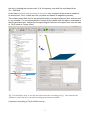
CONCEPT-II
CONCEPT-II is a frequency domain method of moment (MoM) code, under development
at the Institute of Electromagnetic Theory at the Technische Universität Hamburg-Harburg
(www.tet.tuhh.de).
Overview of demo examples
The following demonstration examples for CONCEPT-II will be discussed in
detail ($CONCEPT: home directory of the package):
1. Wire loop, directory $CONCEPT/demo/example1-wire-loop
2. Cylindrical monopole antenna radiating over a finite ground plate,
directory $CONCEPT/demo/example2-monopole-on-plate
3. Box with aperture and internal radiator, directory
$CONCEPT/demo/example3-box-with-aperture
4. Dielectric sphere in a plane wave field, directory
$CONCEPT/demo/example4-dielectric-sphere
In order to find out how CONCEPT-II works it is recommended to start with the example 1
(wire loop)
Important: file names should never contain blanks.
Shortcuts: Help → Navigation
1
Example 2: Cylindrical monopole antenna
radiating over a finite ground plate
It is assumed that the user is already familiar with example 1.
It is recommended to start from an empty directory and set up the simulation
according to Fig 2.
$CONCEPT/demo/example2-monopole-on-plate
Let us consider a thick monopole antenna on a square ground plate in free space. All
dimensions can be taken from Fig 1.
z
y
h=0.5 m
R=50 mm
0.8 m
Wire between cylinder and
finite plate,
generator at the plate side of the
wire
x
0.8 m
Fig 1: Geometry of the structure under investigation
The antenna is formed by a cylinder of 0.5 m height. A wire (length 2 cm, R = 0.5 mm)
serves as connection between cylinder and plate. A power generator at the lower end of
2
the wire is feeding the structure with 1 W. A frequency loop shall be considered from
10,...,300 MHz.
As we have electrical and geometrical symmetry only a quarter of the structure needs to
be discretized. The x-z plane and the y-z plane are planes of magnetic symmetry.
Two surface patch files need to be generated which are called plate.surf and antenna.surf
in our example. The rod connecting the bottom of the cylinder with the plate is contained in
the file generator.wire. Notice the corresponding file names in the project tree, see left side
of Fig 2 (section 'Project View').
Fig 2: In the display area we see the discretized structure according to Fig 1. Note that only the
symmetric parts need to be considered setting up the numerical model.
A structure according to Fig 2 shall be set up.
3
Discretizing the finite ground plate
Activate: CAD tools → Cad tools 2. Click on
. The plate tool window opens (Fig
1 ):
Fig 3: Creating the mesh of a 0.4 m x 0.4 m plate at 600 MHz with 8 basis
functions per wavelength. Using 8 to 10 basis functions per wavelength is a wellknown rule of thumb for electrically large structure parts.
It is assumed that the highest frequency is 600 MHz and that the mesh involves 8 basis
functions per wavelength. This is far higher than the max. applied frequency. By setting an
appropriate combination of frequency and number of patches per wavelength the grid can
be adjusted to the needs. Compute meshes results in a 7 by 7 element mesh. Clicking on
OK provides the surface patch file plate.surf (Output file...) In the general case a plate
does not need to be flat or rectangular. Arbitrary quadrangles can be subdivided.
Near the feed region which is close to (0m, 0m, 0m) we have to expect a rapid variation of
the antenna near field and of the surface current distribution. Hence we should refine the
grid in this region which can conveniently be carried out as follows. Select a preview
pattern in the 'Mesh refinement' section of the Cad tools 1 card.
4
Fig 4: Local mesh refinement close to the antenna feed point, see Fig 2
Activating
means that quadrangles (our case) can be selected by right click to
be subdivided into 4 smaller quadrangles.
Move the mouse pointer over a quadrangle near the left lower corner of the plate and right
click. A preview pattern marks the selected patch. It is suggested that four patches near
the bottom left corner, i.e. near the antenna feed point, should be marked as illustrated in
Fig 4.
Clicking on
or typing 'e' results in the mesh according to Fig 5 . Note that triangles are
generated in the transition region. Each node of a patch has to be connected to the nodes
of all adjacent patches. In other words: the grid must be closed.
Fig 5: Mesh refinement at the bottom left corner near (0m, 0m, 0m)
5
Creating the cylinder
Activate: CAD tools, then click on
. The following window opens:
Fig 6: Only a quarter of a full cylinder will be discretized when clicking on OK or Apply
In order to get a sufficient mesh from a geometrical point of view the 'Number of patches
per wavelength' has been set to 12 and the frequency to 600 MHz, although the max.
applied frequency is only 300 MHz. At this frequency the mesh would be not good enough.
Magnetic symmetry with respect to the y-z plane and the x-z plane has been specified.
Hence only a quarter of a cylinder is generated when pressing OK.
Creating the wire
The wire could be easily introduced as has been described in example 1, simply be
entering the coordinates (0,0,0), (0,0,0.02) under Simulation → Wires → Edit a new wire
file. There is another way of generating wires. Click on the 'Wires' button in the Cad tools
1 section. The 'Add' button will be activated automatically.
6
Now select two nodes as illustrated in Fig 7 by right clicking on the respective nodes.
Notice that a node is picked once the mouse is turned into a cross.
Fig 7: Two patch nodes have been selected be right mouse clicks for
introducing a wire
Clicking on
or typing 'e' gives the following sub-window:
Fig 8: Change the default entries to the ones shown here
OK creates the file generator.wire .
Load the structure into the simulation: Activate the Simulation tab → right click on the top
entry → select Load all files from 'CAD'.
Activate the check marks 'Magn. symmetry, XZ plane' and 'Magn. symmetry, YZ plane'
Frequency sampling
How to do this is indicated in Fig 2. Right click on the the entry Frequency loop for a
special interval → Set frequencies. The shown sub-window opens. One can change for
example the maximum frequency, the minimum frequency, the sampling, the unit etc.. Do
not forget to press Generate values list. Only frequencies appearing in the list are
considered in the simulation.
7
Excitation
Right click on Excitation (see Fig 9) → Ports (power input/voltage input) → Port(s) on
genrator.wire → Set ports → enter wire number 1 and 1 W
Fig 9: Right-clicking on the Excitation line provides the possibility to
switch to a voltage generator for example
The wire where to place the port can be selected by a right click. In general ports can be
placed at the end, center, or at the beginning of a wire. The same statement applies to
lumped loads, voltage generators or current probes on wires.
Checking geometry, starting of the simulation
Once we are sure that all data is right we can immediately start the simulation
.
As a frequency loop has been specified it may take a while for the back end to finish. Note
that a linear system of equations has to be set up and solved for each frequency step. If
unsure how the MoM works refer to Section 4 of the User's manual.
Sometimes it is advantageous to proceed as follows before starting the simulation:
Simulation (see menu bar)→ Run simulation front-end.
Notice the output in the message section under the display area (number of unknowns,
size of system matrix etc.)
Post processing → 'Show complete structure'
Generally all wires are combined into wire.0 and all surfaces into surf.0 . Note that by
hovering the mouse pointer over a node or a patch all available information is printed in a
special line under the display area.
8
Displaying the surface current distribution
For displaying the current distribution:
- Go to Post processing (see Fig 10 )
- Click on
- Enter the values according to Fig 10, the current distribution at 300 MHz has been
selected for representation
Fig 10: Window for controlling the current distribution to be
displayed. It is recommended to enter 16 phase intervals for a movie.
Pressing OK provides the structure including its current distribution at 0° in the display
area. Of course a certain scaling is necessary in order to obtain a view according to Fig
11. Vector and arrow scaling has already been explained in example 1 for the case of a 2D
field distribution.
9
Fig 11: Current distribution at 300 MHz
In order to validate the result, the power budget shall be investigated. Since lumped loads
(resistors) have not been introduced and the whole structure under investigation includes
only perfect conductors the input power should be radiated completely. In other words: the
depicted surface current distribution should be able to radiate the input power of 1W. This
can be achieved numerically only up to a certain degree. For the computation it is
necessary to establish a 3D radiation diagram.
Creating a 3D radiation diagram
- Got to Post processing (see Fig 12)
- Click on
. A sub-window as depicted in Fig 12 shall be computed
In our case we have chosen All frequencies. Hence a 3D pattern will be computed for
10
Fig 12: The electric far field shall be computed
each frequency step, providing a movie showing the frequency dependence of the pattern
development.
Choosing a sufficient number of elements in theta and phi direction is important to resolve
minor lobes that may appear in the general high frequency case (imagine a grid on a unit
sphere, the field is computed at each intersecting point).
Click the Log data tab → 3D rad. Diagram. This displays the output of the diagram
computation in the display area.
Example values, computation by the power flow in the far field (Poynting vector):
10 MHz,
radiated power: 0.9945 W
300 MHz,
radiated power: 0.9935 W
A deviation of 5% between input power and radiated power can be tolerated for a loss-less
structure in practical situations.
Note that Field values are always given in [V]. Divide by the distance in the far field and
get the E field strength in the chosen direction!
Hint: to quickly get back to the already computed surface current distribution at this stage
of post processing, click on the following entry of the post processing tree:
The input impedance as a function of frequency
- Go to Post processing
11
Fig 13: Window for the selection of system responses to be displayed as a function of frequency
- Click on
. A sub-window as shown in Fig 13 opens.
The only available data in this example up to this point is the input impedance which is
automatically stored in case of generator excitation. OK provides the magnitude in the
display area as a function of frequency.
For an enhanced representation click Freq.-domain responses → show results in the
post processing tree. This open the CONCEPT-II Gnuplot front end. Change the default
entries to the entries as shown in Fig 14 and click Run gnuplot .
12
Fig 14: The real and the imaginary part of the antenna input impedance shall be plotted (columns 2
and 3 of the ASCII data file port-zin1.asc; column 1 is the frequency)
The following curves are displayed:
13
Fig 15: The complex input impedance as a function of frequency
As could be expected we have a large negative imaginary part and a very small positive
real part at the low frequency end.
14