1
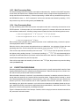
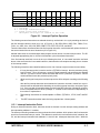
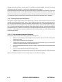
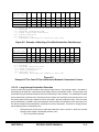
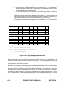
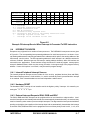
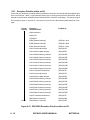
SECTION 8
EXCEPTION PROCESSING
8.1
INTRODUCTION
This section describes the actions of the DSP96002 which are outside the normal processing associated
with the execution of instructions. The sequence of actions taken by the DSP96002 on exception conditions
is described. Also, the interrupt priority level (IPL) of the processor and interrupt sources is described.
8.2
PROCESSING STATES
The DSP96002 is always in one of five processing states: normal, exception, reset, wait, or stop. The normal processing state is that associated with instruction execution.
8.2.1 Exception Processing State
The exception processing state is associated with interrupts. Exception processing may be internally generated by a software interrupt instruction, by an on-chip peripheral hardware interrupt, or by an error condition. Externally, exception processing can be generated by an interrupt. Exception processing provides
an efficient context switch for servicing I/O devices.
8.2.2 Reset Processing State
The reset processing state is entered in response to the external
Upon entering the reset state the following actions occur:
— — — — –
R E S E T pin being asserted.
•
Internal peripheral devices are reset and disabled.
•
The modifier registers Mn are set to $FFFFFFFF.
•
The Interrupt Priority Register (IPR) is cleared.
•
All CCR, ER, IER and MR bits are cleared, except for I1 and I0 in the MR register.
•
The interrupt mask bits I1,I0 in the MR register are set.
— — — — –
The DSP96002 remains in the reset state until R E S E T is deasserted. Upon leaving the reset
state the chip operating mode bits of the operating mode register are loaded from the external Mode Select
pins (MODA, MODB, MODC) and program execution begins at the location described in Section 9.
MOTOROLA
DSP96002 USER’S MANUAL
8-1
8.2.3 Wait Processing State
The wait processing state is a low power consumption mode entered by execution of the WAIT instruction.
In wait mode, the internal clock is disabled from all internal circuitry except the internal peripherals (the interrupt controller and host interfaces). All internal processing is halted until any unmasked interrupt occurs,
— –
— –
the DSP96002 is reset, or D R is asserted. If exit from the wait state was caused by asserting D R,
the processor may enter the debug mode (see Section 10).
8.2.4 Stop Processing State
The stop processing state is the lowest power consumption mode and is entered by the execution of the
STOP instruction. In the stop mode, the clock oscillator is gated off, in contrast to the wait mode where the
clock oscillator remains active. All activity in the processor is halted until one of the following actions occurs:
1. A low level is applied to the —I—R—Q–A pin (—I—R—Q–A asserted)
2. A low level is applied to the —R—E—S—E–T pin (—R—E—S—E–T asserted)
3. A low level is applied to the —D–R pin.
Either of these actions will gate on the oscillator and, after a clock stabilization delay, clocks to the processor and peripherals will be re-enabled.
When the clocks to the processor and peripherals are re-enabled then the processor will enter the reset
— — — — –
processing state if the exit from stop state was caused by a low level on the R E S E T pin.
—— — –
If the exit from stop state was caused by a low level on the I R Q A pin then the processor will service
—— — –
the highest priority pending interrupt. If no interrupt is pending (i. e. I R Q A was deasserted before
interrupts were arbitrated) then the processor resumes execution at the instruction following the STOP instruction that caused the entry into the stop state.
If the exit from stop state was caused by a low level on the
mode (see Section 10).
8.3
— –
D R pin, the processor may enter the debug
EXCEPTION PROCESSING
Exception processing in a digital signal processing environment is primarily associated with transfer of data
between DSP96002 memory or registers and a peripheral device. When an interrupt occurs, a limited context switch must be performed with minimum overhead.
When a hardware interrupt is received, it is synchronized on instruction boundaries so that the first two interrupt instruction words can be inserted into the instruction stream. Suppose that the interrupt is stored
in the interrupt pending latch during the current instruction fetch cycle. During the next cycle, which is the
decode cycle of the current instruction, the PC will be updated to fetch the next instruction. However, in
the following cycle, which is the execution cycle of the current instruction, the address placed on the program address bus (PAB) comes from the appropriate interrupt start address, rather than from the PC. Note
that the PC is frozen until exception processing terminates.
Figure 8-1illustrates the effect of the interrupt controller, which is simply to insert two instruction words into
the processor’s instruction stream.
8-2
DSP96002 USER’S MANUAL
MOTOROLA
Int ctl cyc1
Int ctl cyc2
Fetch
Decode
Execute
*
i
i
n3
n2
n1
i
n4
n3
n2
ii1
n4
n3
ii2
ii1
n4
n5
ii2
ii1
n6
n5
ii2
n7
n6
n5
i
n8
n7
n6
ii3
n8
n7
ii4
ii3
n8
ii4
ii3
i = interrupt
ii = interrupt instruction word
n = normal single word instruction
*
subsequent interrupts are enabled at this time
Figure 8-1. Interrupt Pipeline Operation
The following one-word instructions are aborted when they are fetched in the cycle preceding the fetch of
the first interrupt instruction word (n4 or n8 in Figure 8-1): Bcc, BRA, BScc, BSR, FBcc, FBScc, FJcc,
FJScc, Jcc, JMP, JScc, JSR, LRA, REP, RESET, RTI, RTR, RTS, STOP, and WAIT.
Two-word instructions are aborted when the first interrupt instruction word fetched will replace the fetch of
the second word of the two word instruction (n5 in Figure 8-2).
Aborted instructions are re-fetched again when program control returns from the interrupt routine. The PC
is adjusted appropriately prior to the end of the decode cycle of the aborted instruction.
If the first interrupt word fetch occurs in the cycle following the fetch of a one-word instruction not listed
above or the second word of a two-word instruction, that instruction will complete normally prior to the start
of the interrupt routine.
The following cases have been identified where service of an interrupt might encounter an extra delay:
1.
If a long interrupt routine is used to service a (F)TRAPcc interrupt, then the processor priority
level is set to 3. Thus, all interrupts except for illegal instruction and stack error are disabled
until the (F)TRAPcc service routine terminates with an RTI (unless the (F)TRAPcc service
routine software lowers the processor priority level).
2.
While servicing an interrupt the next interrupt service will be delayed according to the following
rule:
After the first interrupt instruction word reaches the instruction decoder, at least four more instructions will be decoded before decoding the next first interrupt instruction word (see Figure
8-1). If any one pair of instructions being counted is the REP instruction followed by a instruction to be repeated then the whole "package" is counted as two instructions independently of
the number of repeats done.
3.
The following instructions are uninterruptable: ILLEGAL, (F)TRAPcc, STOP, WAIT and RESET.
4.
The REP instruction and the instruction being repeated are uninterruptable.
8.3.1 Interrupt Instruction Fetch
During an interrupt instruction fetch, instruction words are fetched from the interrupt starting address and
interrupt starting address+1 locations.
The interrupt controller generates an interrupt instruction fetch address which points to the first instruction
word of a two-word fast interrupt routine. This address is used for the next instruction fetch, instead of the
PC, and the interrupt instruction fetch address+1 is used for the subsequent instruction fetch. While the
MOTOROLA
DSP96002 USER’S MANUAL
8-3
interrupt instructions are being fetched, the PC is inhibited from being updated. After the two interrupt
words have been fetched, the PC is used for any following instruction fetches.
After both interrupt instructions words have been fetched, they are guaranteed to be executed. This is true
even if the instruction that is currently being executed is a change of flow instruction (i.e., JMP, JSR, etc.)
that would normally ignore the instructions in the pipe. After the interrupt instruction fetch, the PC will point
to the instruction that would have been fetched if the interrupt instructions had not been substituted.
8.3.2 Interrupt Instruction Execution
Two types of interrupt routines may be used: fast and long. The fast routine consists of only the two automatically inserted interrupt instruction words. These words can contain any single two-word instruction or
any two one-word instructions, except for restrictions listed in Section A.9.2.1. Interrupt instruction execution is considered to be fast if neither of the instructions of the interrupt service routine cause a change of
flow. A jump to subroutine within a fast interrupt routine forms a long interrupt. A long interrupt routine is
terminated with an RTI instruction to restore the PC and SR from the stack and return to normal program
execution. Hardware Reset is a special exception which will normally contain only a JMP instruction at the
exception start address.
8.3.2.1 Fast Interrupt Instruction Execution
Execution of a fast interrupt routine always follows the following rules:
1.
Status is not saved during a fast interrupt routine; therefore, instructions which modify status
should not be used.
2.
Fast interrupt routines are never interruptible.
3.
The fast interrupt routine may contain any single two-word instruction or any two one-word instructions, except for restrictions listed in Section A.9.2.1.
4.
If one of the instructions in the fast routine is a jump to subroutine, then a long interrupt routine
is formed.
5.
The PC is never updated during a fast interrupt routine.
6.
Normal instruction fetching resumes using the PC following the completion of the fast interrupt
routine.
Figure 8-3 illustrates the effect of a fast interrupt routine on the instruction pipeline.
8-4
DSP96002 USER’S MANUAL
MOTOROLA
Int ctl cyc1
Int ctl cyc2
Fetch
Decode
Execute
f
i
ii
n
n4
n5
*
=
=
=
=
=
=
*
i
i
n3
n2
n1
i
n4
n3
n2
ii1
n4
n3
ii2
f1
NOP
n4
f2
f1
n5
n4
f2
n6
-n4
i
n7
n6
--
ii3
n7
n6
ii4
f3
n7
n8
f4
f3
fast interrupt instruction word (non-control-flow-change)
interrupt
interrupt instruction word
normal single word instruction
2-word instruction
2nd word of n4
subsequent interrupts are enabled at this time
Figure 8-2. Example of Aborting a Two Word Instruction Fast Interrupt
Int ctl cyc1
Int ctl cyc2
Fetch
Decode
Execute
*
i
i
n3
n2
n1
i
n4
n3
n2
ii1
n4
n3
ii2
f1
n4
n5
f2
f1
n6
n5
f2
n7
n6
n5
i
n8
n7
n6
ii3
-n7
ii4
f3
--
n9
f4
f3
f = fast interrupt instruction word (non-control-flow-change)
i = interrupt
ii = interrupt instruction word
n = normal instruction word
n7 = 2-word instruction
n8 = 2nd word of n7
*
subsequent interrupts are enabled at this time
Figure 8-3.
Example Of The Case Of Four Instructions Between Consecutive Vectors
8.3.2.2 Long Interrupt Instruction Execution
A jump to subroutine instruction within a fast interrupt routine forms a long interrupt routine. One-word or
two-word jump to subroutine instructions may be used to form a long interrupt routine. The one-word jump
to subroutine may be located in either the first or second interrupt vector location. If a conditional one-word
jump to subroutine is located in the first interrupt vector location, the instruction in the second vector location will be ignored if the jump condition is true but executed if the jump condition is false. If the one-word
jump to subroutine is located in the second interrupt vector location, the instruction in the first vector location will be fetched and executed before executing the jump to subroutine. Execution of a long interrupt
routine always follows the following rules:
1.
During execution of the jump to subroutine instruction, when it occurs in the first or second
interrupt vector location, the following actions occur:
1. The PC and SR are stacked.
MOTOROLA
DSP96002 USER’S MANUAL
8-5
2. The status register is modified as follows: the interrupt mask bits I1, I0 in the MR are updated to mask interrupts of the same or lower priority (except that illegal instruction, stack
error and (F)TRAPcc can always interrupt).
3. The PC will be altered by the JSR instruction so that instruction execution will continue
with the instructions located in the address pointed to by the JSR instruction.
2.
Long interrupt routines are interruptible by higher priority interrupts. The first instruction word
of the next interrupt service may reach the decoder only after the decoding of at least four instructions following the decoding of the first instruction of the previous interrupt.
3.
The long interrupt routine should be terminated by an RTI, which pulls the PC and SR from
the stack.
Int ctl cyc1
Int ctl cyc2
Fetch
Decode
Execute
Int ctl cyc1
Int ctl cyc2
Fetch
Decode
Execute
i
ii
JSRf
n
sr
*
=
=
=
=
=
i
n3
n2
n1
i
n4
n3
n2
ii1
n4
n3
ii2
JSRf
n4
sr1
NOP
JSRf
sr2
sr1
NOP
sr3
sr2
sr1
sr4
sr3
sr2
i
n5
NOP
RTI
ii3
n5
NOP
ii4
ii3
n5
n6
ii4
ii3
n7
n6
ii4
n8
n7
n6
n9
n8
n7
*
i
sr5
RTI
sr3
interrupt
interrupt instruction word
fast JSR (one-word JSR instruction)
normal instruction word
service routine word
subsequent interrupts are enabled at this time
Figure 8-4. Long Interrupt Pipeline Action
Figure 8-4 illustrates the effect of a long interrupt routine on the instruction pipeline. A fast JSR (that is, a
one-word JSR instruction) is used to form the long interrupt routine. For this example, word 4 of the long
interrupt routine is an RTI. A subsequent interrupt is shown to illustrate the uninterruptable nature of the
early instructions in the long interrupt routine.
See Figure 8-5 for an example of interrupt service when the instruction that receives the internal interrupt
service request is the REP instruction (n3 in Figure 8-5). During the repeated executions of the instruction
that follows the REP instruction (n4), instruction fetches are suspended. The fetches will be reactivated
only after the loop counter is decremented to one. During the execution of n4, interrupts will not be serviced. When LC finally reaches one, the fetches are reinitiated and the interrupt can be serviced. In Figure
8-5 it can be seen that n5 (loaded into the instruction latch from the backup instruction latch) is decoded
and executed as well as n6 before the first interrupt vector.
8-6
DSP96002 USER’S MANUAL
MOTOROLA
Int ctl cyc1
Int ctl cyc2
Fetch
Decode
Execute
i
ii
n
n3
n4
n5
†
*
=
=
=
=
=
=
i
n3
n2
n1
†
i
n4
REP
n2
i*
n5
NOP
REP
n4
NOP
n4
n4
i
n6
n5
n4
ii1
n6
n5
ii2
ii1
n6
n7
ii2
ii1
n8
n7
ii2
n9
n8
n7
interrupt
interrupt instruction word
normal instruction word
REP #2 instruction
instruction being repeated twice
instruction that waits in the backup instruction latch
interrupt rejected at this time
interrupt can be reenabled at this time
Figure 8-5.
Example Of Interrupt Service When Interrupt Is Presented To REP Instruction
8.4
INTERRUPT SOURCES
Exceptions may originate from a number of interrupt sources. The DSP96002 interrupt sources are given
in Figure 8-6. The corresponding interrupt starting addresses for each interrupt source are shown. Interrupt starting addresses are internally-generated 32-bit addresses which point to the starting address of the
fast interrupt service routine. The interrupt starting address for each interrupt is an address constant for
minimum overhead. Motorola reserves 128 interrupt starting address locations, while 128 locations are
reserved for user applications. These locations occupy the lowest 512 words of program memory space,
except for Hardware Reset, which may also occupy a location in the upper range of the program memory
address. If some of this space is not used, it may be used for program storage.
8.4.1 Internal Peripheral Interrupt Sources
The internal peripheral interrupt sources include all of the on-chip peripheral devices (Host and DMA).
Each internal interrupt source is level sensitive; i.e., each is serviced any time it is present and the interrupt
is not masked. Each internal hardware source has independent enable control.
8.4.2 Hardware RESET
The Hardware RESET interrupt is level sensitive and is the highest priority 3 interrupt. It is caused by as— — — — –
serting the R E S E T pin.
8.4.3 External Interrupt Requests IRQA, IRQB and IRQC
The IRQA, IRQB and IRQC interrupts can be programmed to be level-sensitive or edge-sensitive. Levelsensitive interrupts are not internally latched and are not automatically cleared when they are serviced; they
must be cleared by other means to prevent multiple interrupts. The edge-sensitive interrupts are latched as
pending on the high-to-low transition of the interrupt input and are automatically cleared when the interrupt
is serviced. IRQA, IRQB and IRQC can be programmed to one of three priority levels: level 0, 1, or 2, all of
MOTOROLA
DSP96002 USER’S MANUAL
8-7
Interrupt
Starting
Address
interrupt Source
$FFFFFFFE
$00000000
$00000002
$00000004
$00000006
$00000008
$0000000A
$0000000C
$0000000E
$00000010
$00000012
$00000014
$00000016
$00000018
$0000001A
$0000001C
$0000001E
$00000020
$00000022
$00000024
$00000026
$00000028
$0000002A
$0000002C
$0000002E
$00000030
$00000032
$00000034
$00000036
$00000038
$0000003A
$0000003C
$0000003E
$00000040
:
$000000FE
$00000100
:
$000001FE
Hardware RESET
Hardware RESET
Stack Error
Illegal Instruction
(F)TRAPcc (default)
IRQA
IRQB
IRQC
Reserved
DMA Channel 1
DMA Channel 2
Reserved
Reserved
Reserved
Reserved
Host A Command (default)
Host B Command (default)
Host A Receive Data
Host A Transmit Data
Host A Read X Memory
Host A Read Y Memory
Host A Read P Memory
Host A Write X Memory
Host A Write Y Memory
Host A Write P Memory
Host B Receive Data
Host B Transmit Data
Host B Read X Memory
Host B Read Y Memory
Host B Read P Memory
Host B Write X Memory
Host B Write Y Memory
Host B Write P Memory
Reserved
:
Reserved
User interrupt vector
:
User interrupt vector
Note: User interrupt vector locations are available
for host commands.
Figure 8-6. DSP96002 Interrupt Sources
8-8
DSP96002 USER’S MANUAL
MOTOROLA
which are maskable. Additionally, each of these interrupts has independent enable control. When the IRQA,
IRQB or IRQC interrupts are disabled in the interrupt priority register, pending requests will be discarded,
no new requests will be accepted, and the edge-detection latch will remain in the reset state. Also, if the
interrupt is defined as level-sensitive, its edge-detection latch will remain in the reset state.
Interrupt service, which begins by fetching the instruction word in the first vector location, is considered
finished when the instruction word in the second vector location is fetched. In the case of an edge-sensitive interrupt, the internal latch is automatically cleared when the second vector location is fetched. The fetch
of the first vector location does not guarantee that the second location will be fetched. Figure 8.7 illustrates
the one case where the second vector location is not fetched. In Figure 8.7, the (F)TRAPcc instruction "discards" the fetch of the first interrupt vector to ensure that the (F)TRAPcc vectors will be fetched. Instruction
n4 is decoded as a (F)TRAPcc while ii1 is being fetched. Execution of the (F)TRAPcc requires that ii1 be
discarded and the two (F)TRAPcc vectors (ii3 and ii4) be fetched instead.
8.4.4 (F)TRAPcc (Conditional Software Interrupt Instruction)
The (F)TRAPcc instruction causes a non-maskable interrupt which is serviced immediately following the
(F)TRAPcc instruction if the specified condition is true. (F)TRAPcc is a priority 3 interrupt.
Int ctl cyc1
Int ctl cyc2
Fetch
Decode
Execute
i
i*
ii1
ii3
ii4
n
n4
tr
=
=
=
=
=
=
=
=
i*
i
n3
n2
n1
i
n4 ii1
n3 trap -n2
n3 trap
i
---
---
ii3
---
ii4
JSR
--
tr1
-JSR
tr2
tr1
--
tr3
tr2
tr1
interrupt request
interrupt request generated by (F)TRAPcc
first vector of interrupt i
first (F)TRAPcc vector (one word JSR)
second (F)TRAPcc vector
normal instruction word
(F)TRAPcc, cc condition true
instructions pertaining to the (F)TRAPcc long interrupt routine
Figure 8-7. (F)TRAPcc Instruction Rejecting Another Interrupt
CAUTION
On all level-sensitive interrupts, the Interrupt must be externally released before
interrupts are internally re-enabled or the processor will be interrupted repeatedly
until the interrupt is released.
MOTOROLA
DSP96002 USER’S MANUAL
8-9
I1
0
0
1
1
I0
0
1
0
1
Exceptions
Masked
None
IPL 0
IPL 0,1
IPL 0,1,2
Exceptions Permitted
IPL 0, 1, 2, 3
IPL 1, 2, 3
IPL 2, 3
IPL 3
Figure 8-8. Status Register Interrupt Mask Bits
31
30
29
28
27
26
25
24
**
**
**
**
**
**
**
**
Reserved
23
22
21
20
19
18
17
16
HBL1 HBL0 HAL1 HAL0 D1L1 D1L0 D0L1 D0L0
DMA Channel 0 IPL
DMA Channel 1 IPL
Host A IPL
Host B IPL
15
14
13
12
**
**
**
**
11
10
9
8
IRCS ICL2 ICL1 ICL0
IRQC IPL
IRQC Trigger Mode
IRQC Status
Reserved
7
6
5
4
3
2
1
0
IRBS IBL2 IBL1 IBL0 IRAS IAL2 IAL1 IAL0
IRQA IPL
IRQA Trigger Mode
IRQA Status
IRQB IPL
IRQB Trigger Mode
IRQB Status
Note: Reserved bits read as zero and should be written with zero
for future compatibility.
Figure 8-9. Interrupt Priority Register IPR (Address X:$FFFFFFFF)
8 - 10
DSP96002 USER’S MANUAL
MOTOROLA
xxL1 xxL0
0
0
1
1
0
1
0
1
Enabled
Int. Priority Level (IPL)
no
yes
yes
yes
0
1
2
Figure 8-10. Interrupt Priority Level Bits
IxL2
0
1
Trigger Mode
level
neg. edge
IRxS
0
1
Status
Serviced
Pending
Figure 8-11. External Interrupt Trigger Mode and Status
8.4.5 Illegal Instruction Interrupt
The illegal instruction interrupt is a non-maskable interrupt which is serviced immediately following the illegal instruction interrupt instruction (ILLEGAL) or upon loading an illegal instruction in the instruction latch.
The illegal instruction interrupt is a priority 3 interrupt.
8.4.6 Stack Error Interrupt
The Stack Error interrupt is a priority 3 interrupt. It is generated by turning on the Stack Error flag in the
Stack Pointer register, generally due to improper stack operation. The Stack Error flag will remain set until
it is cleared by some instruction that explicitly writes into the SP register. Since the IPL level (3) of this
interrupt does not mask other pending interrupts of this same level, it is recommended that the Stack Error
flag be cleared by the first instruction of the Stack Error interrupt service routine in order not to get the same
request again.
8.5
INTERRUPT PRIORITY STRUCTURE
Four levels of interrupt priority are provided. Interrupt priority levels (IPLs) numbered 0, 1, and 2, are
maskable. Level 0 is the lowest level. Level 3 is the highest level, and is nonmaskable. The only level 3
interrupts are Stack Error, Reset, Illegal Instruction (ILLEGAL) and (F)TRAPcc. The interrupt mask bits (I1,
I0) in the status register reflect the current processor priority level and indicate the interrupt minimum priority
level needed for an interrupt source to interrupt the processor. Figure 8-8 gives a description of the interrupt
mask bits. Interrupts are inhibited for all priority levels less than the current processor priority level. Level
3 interrupts can always interrupt the processor.
8.5.1 Interrupt Priority Levels (IPL)
The interrupt priority level for each on-chip peripheral device (Host, DMA) and for each external interrupt
source (IRQA, IRQB, IRQC) can be programmed under software control. Each on-chip or external peripheral device can be programmed to one of the three maskable priority levels (IPL 0, 1, or 2). Interrupt priority
levels are set by writing to the Interrupt Priority Register.
MOTOROLA
DSP96002 USER’S MANUAL
8 - 11
8.5.2 Interrupt Priority Register (IPR)
This read/write register specifies the interrupt priority level for each of the interrupting devices (Host, DMA,
IRQA, IRQB, IRQC). In addition, this register specifies the trigger mode of each external interrupt source
and shows the status of the external interrupt request. The register is cleared on Hardware reset or by the
RESET instruction. The Interrupt Priority Register is shown in Figure 8-9. Figure 8-10 defines the interrupt
priority level bits. Figure 8-11 defines the external interrupt trigger mode bits and status information.
8.5.2.1 IRQA Interrupt Priority Level - IAL1-IAL0 (Bits 0-1)
The IRQA Interrupt Priority Level (IAL1-IAL0) bits are used to enable and specify the priority level of the
external interrupt input IRQA.
IAL1 IAL0
0
0
0
1
1
0
1
1
8.5.2.2
Enabled
no
yes
yes
yes
Int. Priority Level (IPL)
0
1
2
IRQA Trigger Mode - IAL2 (Bit 2)
The IRQA Trigger Mode (IAL2) bit specifies the trigger method for the external interrupt input IRQA.
IAL2
0
1
8.5.2.3
Trigger Mode
level
negative edge
IRQA Status - IRAS (Bit 3)
The read-only IRQA Status (IRAS) bit indicates the status of the interrupt request for the external interrupt
input IRQA. If the IRQA interrupt is defined as edge-sensitive and it is enabled, the IRAS bit indicates
the state of the edge-detection latch. If the IRQA interrupt is defined as level-sensitive or is disabled,
the IRAS bit indicates the state of the IRQA pin after internal synchronization.
IRAS
0
1
8.5.2.4
Status (edge and enabled) IRQA pin (level or disabled)
Serviced
High
Pending
Low
IRQB Interrupt Priority Level - IBL1-IBL0 (Bits 4-5)
The IRQB Interrupt Priority Level (IBL1-IBL0) bits are used to enable and specify the priority level of the
external interrupt input IRQB.
8 - 12
DSP96002 USER’S MANUAL
MOTOROLA
IBL1 IBL0
0
0
0
1
1
0
1
1
Enabled
no
yes
yes
yes
Int. Priority Level (IPL)
0
1
2
8.5.2.5 IRQB Trigger Mode - IBL2 (Bit 6)
The IRQB Trigger Mode (IBL2) bit specifies the trigger method for the external interrupt input IRQB.
IBL2
0
1
Trigger Mode
level
negative edge
8.5.2.6 IRQB Status - IRBS (Bit 7)
The read-only IRQB Status (IRBS) bit indicates the status of the interrupt request for the external interrupt
input IRQB. If the IRQB interrupt is defined as edge-sensitive and it is enabled, the IRBS bit indicates the
state of the edge-detection latch. If the IRQB interrupt is defined as level-sensitive or is disabled, the
IRBS bit indicates the state of the IRQB pin after internal synchronization.
IRBS
0
1
8.5.2.7
Status (edge and enabled) IRQB pin (level or disabled)
Serviced
High
Pending
Low
IRQC Interrupt Priority Level - ICL1-ICL0 (Bits 8-9)
The IRQC Interrupt Priority Level (ICL1-ICL0) bits are used to enable and specify the priority level of the
external interrupt input IRQC.
ICL1 ICL0
0
0
0
1
1
0
1
1
Enabled
no
yes
yes
yes
Int. Priority Level (IPL)
0
1
2
8.5.2.8 IRQC Trigger Mode - ICL2 (Bit 10)
The IRQC Trigger Mode (ICL2) bit specifies the trigger method for the external interrupt input IRQC.
MOTOROLA
DSP96002 USER’S MANUAL
8 - 13
ICL2
0
1
Trigger Mode
level
negative edge
8.5.2.9 IRQC Status - IRCS (Bit 11)
The read-only IRQC Status (IRCS) bit indicates the status of the interrupt request for the external interrupt
input IRQC. If the IRQC interrupt is defined as edge-sensitive and it is enabled, the IRCS bit indicates
the state of the edge-detection latch. If the IRQC interrupt is defined as level-sensitive or is disabled,
the IRCS bit indicates the state of the IRQC pin after internal synchronization.
IRCS
0
1
8.5.2.10
Status (edge and enabled) IRQC pin (level or disabled)
Serviced
High
Pending
Low
Reserved bits (Bits 12-15, 24-31)
These reserved bits read as zero and should be written with zero for future compatibility.
8.5.2.11 DMA Channel 0 Interrupt Priority Level - D0L1-D0L0 (Bits 16-17)
The DMA Channel 0 Interrupt Priority Level (D0L1-D0L0) bits are used to enable and specify the priority
level of the DMA Channel 0 interrupt.
D0L1 D0L0
0
0
0
1
1
0
1
1
Enabled
no
yes
yes
yes
Int. Priority Level (IPL)
0
1
2
8.5.2.12 DMA Channel 1 Interrupt Priority Level - D1L1-D1L0 (Bits 18-19)
The DMA Channel 1 Interrupt Priority Level (D1L1-D1L0) bits are used to enable and specify the priority
level of the DMA Channel 1 interrupt.
D1L1 D1L0
0
0
0
1
1
0
1
1
8.5.2.13
Enabled
no
yes
yes
yes
Int. Priority Level (IPL)
0
1
2
Host A Interrupt Priority Level - HAL1-HAL0 (Bits 20-21)
The Host A Interrupt Priority Level (HAL1-HAL0) bits are used to enable and specify the priority level of all
interrupt sources located in the Port A Host Interface.
8 - 14
DSP96002 USER’S MANUAL
MOTOROLA
HAL1 HAL0
0
0
0
1
1
0
1
1
Enabled
no
yes
yes
yes
Int. Priority Level (IPL)
0
1
2
8.5.2.14 Host B Interrupt Priority Level - HBL1-HBL0 (Bits 22-23)
The Host B Interrupt Priority Level (HBL1-HBL0) bits are used to enable and specify the priority level of all
interrupt sources located in the Port B Host Interface.
HBL1 HBL0
0
0
0
1
1
0
1
1
MOTOROLA
Enabled
no
yes
yes
yes
Int. Priority Level (IPL)
0
1
2
DSP96002 USER’S MANUAL
8 - 15
8.5.3 Exception Priorities within an IPL
If more than one exception is pending when an instruction is executed, the interrupt with the highest priority
level is serviced first. Within a given interrupt priority level, a second priority structure determines which
interrupt is serviced when multiple interrupt requests with the same IPL are pending. The priority of equal
IPL interrupts is given in Figure 8-12. Also given in Figure 8-12 are the interrupt enable bits for all interrupts.
Priority
highest
lowest
Exception
Hardware RESET
Enabled by
-
Illegal Instruction
-
Stack Error
-
(F)TRAPcc
-
IRQA (External Interrupt)
(IPR) IAL1-IAL0
IRQB (External Interrupt)
(IPR) IBL1-IBL0
IRQC (External Interrupt)
(IPR) ICL1-ICL0
Host A Command Interrupt
(HCR) HCIE
Host A Receive Data Interrupt
(HCR) HRIE
Host A Read X Memory Interrupt
(HCR) HXRE
Host A Read Y Memory Interrupt
(HCR) HYRE
Host A Read P Memory Interrupt
(HCR) HPRE
Host A Write X Memory Interrupt
(HCR) HXWE
Host A Write Y Memory Interrupt
(HCR) HYWE
Host A Write P Memory Interrupt
(HCR) HPWE
Host A Transmit Data Interrupt
(HCR) HTIE
Host B Command Interrupt
(HCR) HCIE
Host B Receive Data Interrupt
(HCR) HRIE
Host B Read X Memory Interrupt
(HCR) HXRE
Host B Read Y Memory Interrupt
(HCR) HYRE
Host B Read P Memory Interrupt
(HCR) HPRE
Host B Write X Memory Interrupt
(HCR) HXWE
Host B Write Y Memory Interrupt
(HCR) HYWE
Host B Write P Memory Interrupt
(HCR) HPWE
Host B Transmit Data Interrupt
(HCR) HTIE
DMA Channel 0 Interrupt
(DCS0) DIE0
DMA Channel 1 Interrupt
(DCS1) DIE1
Figure 8-12. DSP96002 Exception Priorities within an IPL
8 - 16
DSP96002 USER’S MANUAL
MOTOROLA