1
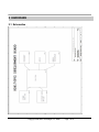
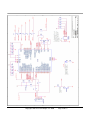
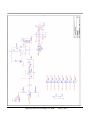
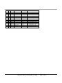
RDB1768V2 Development Board
User Manual
2/27/2010
Rev.1
Copyright Code Red Technologies Inc. 2009
Page 1 of 18
1
2
OVERVIEW
1.1
LPC1768 Features
3
1.2
RDB1768V2 Evaluation Board Hardware
3
COMPONENTS
2.1
3
3
5
Component descriptions
5
HARDWARE
7
3.1
Schematics
7
3.2
Mapping of peripherals to LPC1768 IO pins
14
4
IO PADS FOR EXTERNAL CONNECTION
16
5
DEVELOPING AND DEBUGGING
17
6
REFERENCES
18
Copyright Code Red Technologies Inc. 2009
Page 2 of 18
1 OVERVIEW
The RDB1768V2 Evaluation Board gives a solid development platform for the development of systems around the
NXP LPC1768 Cortex-M3 based Microcontroller. The LPC1768 is the ‘superset’ part of the LPC17xx family, and
therefore the RDB1768 makes an excellent development board for the whole LPC17xx family of parts.
The board allows the rapid prototyping of embedded systems through the use of the on-board peripheral interfaces
and supplied example software, or by connecting external hardware to the IO pads.
1.1 LPC1768 Features
•
512K Bytes of on-chip FLASH
•
64K Bytes on-chip SRAM (in 2 banks)
•
10/100 Ethernet MAC with external PHY interface
•
USB Host/Device OTG controller and PHY. USB 2 full-speed
•
I2S Digital Audio interface
•
3 I2C interfaces
•
2 SSP interfaces
•
1 SPI interface
•
2 CAN interfaces
•
8-channel, 12-bit on-chip ADC
•
10-bit on-chip DAC
•
PWM generation
•
Quadrature Encoder Interface
•
4 GP Timers
•
Ultra low-power Real-Time-Clock
•
Up to 70 GPIO pins
1.2 RDB1768V2 Evaluation Board Hardware
•
Drag2FLASH feature makes board appear as mass storage device for simple binary file FLASHing
•
LPC1768 running at 100MHz
•
128x128 pixel color LCD display driven by GPIO port pins
•
Ethernet PHY – SMSC LAN8720
•
USB Device interface with standard ‘Mini-B’ connector
•
USB Host interface with standard ‘A’ connector
•
On-board USB debug interface (no need for a debug probe)
Copyright Code Red Technologies Inc. 2009
Page 3 of 18
•
UDA1380 Stereo Audio codec connected to the LPC1768 I2S port with Headphone-out, Line-out, Line-in and
Mic-in connectors. UDA1380 configuration uses I2C0. Rx and Tx I2S are decoupled so different sample rates
can be used.
•
Micro-SD card socket wired to SSP0/SPI port
•
RS232 COM port interface on UART0 of LPC1768. Can be used to program LPC1768 FLASH in In-System
Programming (ISP) mode
•
Switching mini-Joystick with left, right, up, down and select outputs
•
On board amplifier and speaker can be driven by UDA1380 codec and/or LPC1768 DAC
•
Potentiometer connected to ADC input
•
12MHz Crystal for the main LPC1768 clock (simple multiple for USB)
•
25MHz Crystal for the Ethernet PHY
•
On board regulators for 3v3 derived from Debug USB Mini-B, USB Device Mini-B or Power connector
•
All on-board peripherals can be disconnected by removable links on the board. All LPC1768 IO pins
brought out to pin-thro pads for connection of external peripherals. For more information see section
4.
Copyright Code Red Technologies Inc. 2009
Page 4 of 18
2 COMPONENTS
2.1 Component descriptions
NAME
DESCRIPTION
COM
RS232 COM port connected to UART0 on the LPC2368
S1
Dual DIP switch to allow configuration of ISP through the COM
port
USB Dev
USB Device Mini-B connector. Can be used to power the board.
USB Host
USB Host ‘A’ connector. Can supply power to peripherals. Is
limited to 500mA, but if board is being powered from one of it’s
USB device sockets then the capability will be less
LED1
LED1 indicates when an external debug probe is connected to the
Copyright Code Red Technologies Inc. 2009
Page 5 of 18
JTAG/SWD connector
LED 2-5
User LEDS connected to P1_24, P1_25, P1_28, P1_29
NAME
DESCRIPTION
MicroSD
Micro-SD Card socket. Pins connect to SSI0/SPI on the LPC1768
Display
128x128 pixel color LCD display
RST
Reset button for processor
ISP
ISP button. Hold down with RST, then release RST first to enter
ISP mode
ETH
The Ethernet connector
TP2
Scope probe GND post
Line-in
Stereo 3.5mm connector line level input connector to the audio
codec
Mic-in
Sensitive mic input to the audio codec
S2
Dual DIP switch to select the source of audio to the speaker.
Either the Codec, the DAC or a mix of both.
Headphone
Stereo 3.5mm connector for driving audio headphones
Line-out
Stereo 3.5mm line-level output from the audio codec
Debug
USB Mini-B connector for use of ‘on-board’ debug – direct connect
to PC for debug with Red Suite. Can be used to power the board.
JTAG/SWD
Standard 0.05” pitch 2x5 pin JTAG/SWD connector for use of
external debug probe such as Red Probe
PSU
External power supply connector – 5V D.C. regulated
TP1
Scope probe GND post
LED6
The power-on LED
LED7
USB device ‘Goodlink’ LED
UH1, UH2
User Headers with all IO pins
Speaker
Speaker driven from either on-chip DAC, or audio codec. Source is
selected by S2.
Joystick
4-way + select, switch style joystick
ADC Pot
Potentiometer connected to Analogue to Digital Convertor (ADC)
of LPC1768
Copyright Code Red Technologies Inc. 2009
Page 6 of 18
3 HARDWARE
3.1 Schematics
Copyright Code Red Technologies Inc. 2009
Page 7 of 18
Copyright Code Red Technologies Inc. 2009
Page 8 of 18
Copyright Code Red Technologies Inc. 2009
Page 9 of 18
Copyright Code Red Technologies Inc. 2009
Page 10 of 18
Copyright Code Red Technologies Inc. 2009
Page 11 of 18
Copyright Code Red Technologies Inc. 2009
Page 12 of 18
Copyright Code Red Technologies Inc. 2009
Page 13 of 18
3.2 Mapping of peripherals to LPC1768 IO pins
Port
Bit
MODE
Usage
PERIPHERAL
JOYSTICK
0
0
GPIO
joystick left
0
1
GPIO
joystick right
JOYSTICK
0
2
UART
UART_TXD
COM
0
3
UART
UART_RXD
COM
0
4
GPIO
joystick up
JOYSTICK
0
5
GPIO
joystick down
JOYSTICK
0
6
GPIO
joystick click
JOYSTICK
0
7
I2S
I2STX_CLK
AUDIO
0
8
I2S
I2STX_WS
AUDIO
0
9
I2S
I2STX_SDA
AUDIO
0
10
GPIO
CODEC_RESET
AUDIO
0
15
SPI
sd_sck
SD
0
16
SPI
sd_cs
SD
0
17
SPI
sd_do
SD
0
18
SPI
sd_di
SD
0
23
ADC
POTENTIOMETER
POT
0
25
I2S
I2SRX_SDA
AUDIO
0
26
DAC
DACOUT
AUDIO
0
27
I2C
SDA
AUDIO
0
28
I2C
SCL
AUDIO
0
29
USB
USB DEVICE D+
USB
0
30
USB
USB DEVICE D-
USB
1
0
ETH
txd_0
ETHERNET
1
1
txd_1
ETHERNET
1
4
tx_en
ETHERNET
1
8
CRS
ETHERNET
1
9
RXD_0
ETHERNET
rxd_1
ETHERNET
rx_er
ETHERNET
1
10
1
14
1
16
1
17
1
18
1
1
ETH
ETH
ETH
ETH
ETH
ETH
ETH
COMMENTS
mdc
ETHERNET
mdio
ETHERNET
USB
USB GOODLINK LED
USB
19
USB
usb_port_pwr
USB
22
USB
usb_ppwrd#
USB
1
24
GPIO
LED2 (USER)
LED
1
25
GPIO
LED3 (USER)
LED
1
27
USB
usb_ovrcr
USB
1
28
GPIO
LED4 (USER)
LED
1
29
GPIO
LED5 (USER)
LED
1
30
USB
USBDEV VBUS
USB
Detect VBUS
2
0
GPIO
db0
display
PIN 19 of ST7637 display controller
2
1
GPIO
db1
display
PIN 18 of ST7637 display controller
2
2
GPIO
db2
display
PIN 17 of ST7637 display controller
2
3
GPIO
db3
display
PIN 16 of ST7637 display controller
ETH
USB HOST POWER ENABLE
Overcurrent detect on the USB HOST
Copyright Code Red Technologies Inc. 2009
Page 14 of 18
PORT
MODE
USAGE
PERIPHERAL
COMMENTS
2
BIT
4
GPIO
db4
display
PIN 15 of ST7637 display controller
2
5
GPIO
db5
display
PIN 14 of ST7637 display controller
2
6
GPIO
db6
display
PIN 13 of ST7637 display controller
2
7
GPIO
db7
display
PIN 12 of ST7637 display controller
2
8
GPIO
A0
display
PIN 9 of ST7637 display controller
2
9
USB
USB CONNECT
USB
2
10
ISP BOOT
ISP BOOT
2
11
GPIO
WR
display
PIN 10 of ST7637 display controller
2
12
GPIO
RD
display
PIN 11 of ST7637 display controller
2
13
GPIO
CSB (chip select)
display
PIN 7 of ST7637 display controller
3
25
GPIO
RESB (reset)
display
PIN 8 of ST7637 display controller
4
28
GPIO
TX_MCLK
AUDIO
Copyright Code Red Technologies Inc. 2009
Page 15 of 18
4 IO PADS FOR EXTERNAL CONNECTION
On the RDB1768, all of the peripherals on the board can be electrically isolated from the LPC1768 through the
removal of links on the board. These are all labelled on the board. For example if the link labelled ‘LK2_0’ is removed,
this will disconnect the display from IO pin P2_0. This will then allow the user to add any external peripheral using
P2_0, connecting through the user headers UH1 and UH2.
The pinouts for user headers UH1 and UH2 can be seen on the schematics and below.
Copyright Code Red Technologies Inc. 2009
Page 16 of 18
5 DEVELOPING AND DEBUGGING
The RDB1768 is designed to interface seamlessly with the Red Suite Development Environment from Code Red
Technologies. Simply connecting a PC to the RDB1768 with the USB debug port enables Red Suite to be used as
your code development and debugging environment.
TM
The Drag2FLASH feature allows users to simply drag built binary files onto an Explorer window and press the
button to FLASH the LPC1768 and start running the code.
The board also has a standard 10-pin 0.05” pitch JTAG/SWD connector. An external debug probe can be connected
to this port for debugging. Red Probe from Code Red Technologies can be used with Red Suite 2 and connected
directly to this connector. Alternatively, other debug probes and tool chains may be connected through this standard
connector pin-out.
Copyright Code Red Technologies Inc. 2009
Page 17 of 18
6 REFERENCES
1. CODE RED TECHNOLOGIES SUPPORT WIKI:
www.code-red-tech.com/CodeRedWiki
2. NXP LPC17xx USER MANUAL:
http://www.standardics.nxp.com/products/lpc1000/all/
3. NXP LPC17xx DATA SHEETS:
http://www.standardics.nxp.com/products/lpc1000/all/
4. ARM CORTEX-M3 TECHNICAL REFERENCE MANUAL:
http://infocenter.arm.com/help/index.jsp?topic=/com.arm.doc.ddi0337g/index.html
5. FORMIKE KWH0151DN01-061A 128X128 COLOR DISPLAY SPECIFICATION
Supplied as pdf.
6. SITRONIX ST7637 DISPLAY DRIVER DATA SHEET (AS USED ON ABOVE DISPLAY MODULE)
Supplied as pdf.
7. National Semiconductor DP83848C PHYTER ETHERNET PHY DATASHEET:
http://www.national.com/pf/DP/DP83848C.html
8. Cirrus Logic CS42L51 audio codec data sheet:
http://www.cirrus.com/en/products/pro/detail/P1088.html
Copyright Code Red Technologies Inc. 2009
Page 18 of 18