1
CUSTOMER NOTIFICATION
SBA1-070002-00 (1/138)
April 6, 2007
Yoshikazu Saotome, Manager
Sales Sect. First Sales Dept.
System Equipment Div.
Naito Densei Machida Mfg. Co., Ltd.
FL-PR5
User’s Manual (Provisional)
Naito Densei Machida Mfg. Co., Ltd.
Date Published April 6, 2007 (1st edition)
URL: http://www.ndk-m.co.jp/asmis/
Flash Memory Programmer FL-PR5 User’s Manual (Provisional)
[MEMO]
SBA1-070002-00
2/138
Flash Memory Programmer FL-PR5 User’s Manual (Provisional)
SBA1-070002-00
3/138
PREFACE
Target Readers
This manual is intended for users who use the FL-PR5 (hereinafter referred to as FP5)
when designing and developing a system using an NEC Electronics on-chip flash
memory micro controller.
Purpose
This manual is intended to give users an understanding of the basic specifications and
correct use of the FP5.
Organization
This manual includes the following sections.
Overview
Hardware installation
Software installation
Programming GUI usage
Example of operation using programming GUI
FL-PR5 operation in standalone mode
Connectors and cables
Notes on target system designs
Target interface specifications
Troubleshooting
Error messages
Supplementary information
How to Read This Manual It is assumed that the readers of this manual have general knowledge of electricity,
logic circuits, and micro controllers. In the explanations of the operation of the
applications, it is also assumed that the readers have sufficient knowledge of Windows.
®
For the usage and terminology of Windows , refer to each Windows manual.
To understand the overall operation
Read this manual according to the CONTENTS.
To know the cautions of target system
See the CHAPTER 7 CONNECTORS AND CABLES, CHAPTER 8 NOTES ON
TARGET SYSTEM DESIGNS, and CHAPTER 9 SPECIFICATION OF TARGET
INTERFACE CIRCUITS.
Also see the user’s manual for each target device.
Flash Memory Programmer FL-PR5 User’s Manual (Provisional)
Conventions
Note:
SBA1-070002-00
4/138
Footnote for item marked with Note in the text.
Caution:
Information requiring particular attention
Remark:
Supplementary information
Numeral representation: Binary ... or B
Decimal ...
Hexadecimal ... 0H or H
Terminology
“
”:
Any character or item on screen
[
]:
Name of commands, dialog boxes or area
The meanings of the terms used in this manual are as follows.
Term
Meaning
FP5
Abbreviation of the flash memory programmer FL-PR5
Programming GUI
Windows application to operate FP5 using programming GUI
Target device
NEC Electronics on-chip flash memory micro controller
Target system
Program adapter
PR5 file
User-designed board on which target device is mounted
Note
Conversion adapter to write programs to target device
Text file containing programming information specific to the target device
(Parameter file (*.pr5) for PG-FP5, a product of NEC Electronics)
ESF file
Text file containing programming environment settings specified with programming GUI
(Customized setup file (*.esf) for FP5)
Program file
HEX file of Intel HEX format type or Motorola HEX format type
Note The program adapter (FA-xxxx) is a product of Naito Densei Machida Mfg. Co., Ltd.
Flash Memory Programmer FL-PR5 User’s Manual (Provisional)
SBA1-070002-00
5/138
General Precautions on Handling This Product
1.
Circumstances not covered by product guarantee
If the product was disassembled, altered, or repaired by the customer
If it was dropped, broken, or given another strong shock
Use at overvoltage, use outside guaranteed temperature range, storing outside guaranteed temperature range
If power was turned on while the AC adapter, interface cable, or connection to the target system was in an
unsatisfactory state
If the cable of the AC adapter, the interface cable, the target cable, or the like was bent or pulled excessively
If an AC adapter other than the supplied product was used
If the product got wet
If the product and target system were connected while a potential difference existed between the GND of the
product and the GND of the target system
If a connector or cable was connected or disconnected while power was being supplied to the product
If an excessive load was applied to a connector or cable
If the product is used or stored in an environment where an electrostatic or electrical noise is likely to occur
2.
Safety precautions
If used for a long time, the product may become hot (50 to 60C).
Be careful of low temperature burns and
other dangers due to the product becoming hot.
Be careful of electrical shock. There is a danger of electrical shock if the product is used as described above in
1 Circumstances not covered by product guarantee.
The AC adapter supplied with the product is exclusively for this product, so do not use it with other products.
Flash Memory Programmer FL-PR5 User’s Manual (Provisional)
SBA1-070002-00
6/138
CONTENTS
CHAPTER 1 OVERVIEW............................................................................................................................................ 9
1.1 Features ............................................................................................................................................................ 9
1.2 Writing Quality ................................................................................................................................................... 9
1.3 Supported Devices ............................................................................................................................................ 9
1.4 FP5 System Overview ..................................................................................................................................... 10
1.5 Operating Environment.................................................................................................................................... 11
1.6 Hardware Specifications .................................................................................................................................. 13
CHAPTER 2 HARDWARE CONFIGURATION ......................................................................................................... 14
2.1 Package Contents ........................................................................................................................................... 14
2.2 System Configuration ...................................................................................................................................... 14
2.3 Names and Functions on Main Unit................................................................................................................. 16
CHAPTER 3 SOFTWARE INSTALLATION .............................................................................................................. 19
3.1 Obtaining Software .......................................................................................................................................... 19
3.2 Installation ....................................................................................................................................................... 19
3.3 Uninstallation ................................................................................................................................................... 24
3.4 Updating Programming GUI, Firmware and FPGA .......................................................................................... 25
CHAPTER 4 PROGRAMMING GUI USAGE ............................................................................................................ 35
4.1 Introduction...................................................................................................................................................... 35
4.2 Startup of Programming GUI ........................................................................................................................... 35
4.3 Menu Bar ......................................................................................................................................................... 38
4.4 Toolbar ............................................................................................................................................................ 85
4.5 Action Log Window .......................................................................................................................................... 86
4.6 Programming Parameter Window.................................................................................................................... 87
4.7 Status Bar........................................................................................................................................................ 88
4.8 Hint Bar............................................................................................................................................................ 89
CHAPTER 5 EXAMPLE OF OPERATION USING PROGRAMMING GUI ............................................................... 90
CHAPTER 6 USAGE IN STANDALONE MODE .................................................................................................... 103
6.1 Before Starting Standalone Operation ........................................................................................................... 103
6.2 Description of Buttons, Message Display and Status LEDs........................................................................... 103
6.3 Standalone Operation Menu .......................................................................................................................... 105
CHAPTER 7 CONNECTORS AND CABLES ......................................................................................................... 110
7.1 Power Supply Connector ............................................................................................................................... 110
7.2 Serial Connector ............................................................................................................................................ 111
7.3 USB Connector.............................................................................................................................................. 112
7.4 Target Connector........................................................................................................................................... 113
7.5 GND Connector ............................................................................................................................................. 115
CHAPTER 8 NOTES ON TARGET SYSTEM DESIGN .......................................................................................... 116
CHAPTER 9 SPECIFICATIONS OF TARGET INTERFACE CIRCUITS................................................................. 120
9.1 SO/TxD, RESET and SCK............................................................................................................................. 120
9.2 SI/RxD and H/S ............................................................................................................................................. 120
9.3 CLK................................................................................................................................................................ 121
9.4 FLMD0 and FLMD1 ....................................................................................................................................... 121
9.5 VDD and VDD2.............................................................................................................................................. 122
9.6 VPP ............................................................................................................................................................... 122
CHAPTER 10 TROUBLESHOOTING..................................................................................................................... 123
10.1 Problems During Startup ............................................................................................................................. 123
10.2 Problems During Operation ......................................................................................................................... 124
APPENDIX A MESSAGES ..................................................................................................................................... 127
Flash Memory Programmer FL-PR5 User’s Manual (Provisional)
SBA1-070002-00
7/138
A.1 Message Format ........................................................................................................................................... 127
A.2 Error/Warning Dialog Boxes for Programming GUI Operation ...................................................................... 128
A.3 Information Dialog Boxes for Programming GUI Operation........................................................................... 131
A.4 Error Messages Displayed in FP5 Message Display..................................................................................... 133
APPENDIX B SUPPLEMENTARY INFORMATION ................................................................................................ 135
APPENDIX C REVISION HISTORY........................................................................................................................ 138
Flash Memory Programmer FL-PR5 User’s Manual (Provisional)
SBA1-070002-00
8/138
Windows is a registered trademark or a trademark of Microsoft Corporation in the United States and/or other countries.
PC/AT is a trademark of International Business Machines Corporation.
・ The information in this document is subject to change without notice.
・ No part of this document may be copied or reproduced in any form or by any means without prior written
consent of Naito Densei Machida. Naito Densei Machida assumes no responsibility for any errors that may
appear in this document.
・ Naito Densei Machida does not assume any liability for infringement of patents, copyrights or other
intellectual property rights of third parties by or arising from the use of such products. No license, express,
implied or otherwise, is granted under any patents, copyrights or other intellectual property rights of Naito
Densei Machida or others.
・ Descriptions of circuits, software and other related information in this document are provided for illustrative
purpose in semiconductor product operation and application examples. The incorporation of these circuits,
software and information in the design of a customer’s equipment shall be done under the full responsibility
of the customer. Naito Densei Machida assumes no responsibility for any losses incurred by customers or
third parties arising from the use of these circuits, software and information.
・ While Naito Densei Machida endeavors to enhance the quality, reliability and safety of Naito Densei
Machida products, customers agree and acknowledge that the possibility of defects thereof cannot be
eliminated entirely. To minimize risks of damage to property or injury (including death) to persons arising
from defects in Naito Densei Machida products, customers must incorporate sufficient safety measures in
their design, such as redundancy, fire-containment and anti-failure features.
(Note)
(1) “Naito Densei Machida” as used in this statement means Naito Densei Machida Mfg. Co., Ltd. and also
includes its majority-owned subsidiaries.
(2) “Naito Densei Machida products” means any product developed or manufactured by or for Naito Densei
Machida (as defined above).
Flash Memory Programmer FL-PR5 User’s Manual (Provisional)
SBA1-070002-00
9/138
CHAPTER 1 OVERVIEW
The FP5 is a tool that erases, writes and verifies programs on an NEC Electronics on-chip flash memory micro
controller on the target system or program adapter.
1.1
Features
Supports on-chip 2-power-supply flash memory micro controllers and single-power-supply on-chip flash memory
micro controllers
Supports flash memory programming through the programming GUI using the host machine (programming GUI
operation) and operation in standalone (standalone operation)
Supports on-board programming through which programs are written with the target device mounted on the target
system, and off-board programming through which programs are written via a program adapter without the target
device mounted on the target system
Program files can be saved in the 16 MB flash memory in the FP5 (divided by 4, in 4 MB units or divided by 8, in
2 MB units)
Device-specific parameters required for programming can be saved in the FP5 internal flash memory by using the
parameter file (PR5 file) for PG-FP5, a product of NEC Electronics, together with programming settings (ESF file).
Multiple program files, PR5 files and ESF files can be saved
Supports CSI, CSI + HS, UART, I C and PORT as target device interfaces
2
Can supply VDD and clocks to the target device
Supports USB interface and serial interface (RS-232C) as a host interface
Supports self-testing function
Can update firmware and FPGA
Compact and lightweight
Compatible with PG-FP5, a product of NEC Electronics
1.2
Writing Quality
Thoroughly confirm, verify and evaluate the following points before using the FP5, in order to improve the writing
quality.
Design circuits as described in the user’s manual for the target device and the FP5.
Use the device and the FP5 as described in the user’s manual for each product.
The power supplied to the target device is stable.
1.3
Supported Devices
The FP5 supports on-chip 2-power-supply flash memory micro controllers and on-chip single-power-supply flash
memory micro controllers.
FP5 parameter files (PR5 files) corresponding to the supported devices are posted on the following website of NEC
Electronics.
URLs Japanese version: http://www.necel.com/micro/ods/jpn/
English version:
http://www.necel.com/micro/ods/eng/ Click “Version-up Service”.
Select the micro controller to be used in the Each Device Series column and select the device name in the
Device Name column; the FP5 parameter file can then be found.
Flash Memory Programmer FL-PR5 User’s Manual (Provisional)
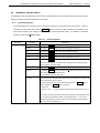
1.4
SBA1-070002-00
10/138
FP5 System Overview
The FP5 system overview is shown in the following diagrams.
Figure 1-1.
FP5 Connection Image
Figure 1-2.
FP5 Function Overview
Serial cable
PR5 file
ESF file
USB cable
AC adapter
Programming
environment setting
HEX editor changes
the memory contents
Checksum calculation
Self-testing function
Saved in FP5 internal
flash memory
16MB
Buzzer function
Saving log files
Standalone operation
Downloading
program files
Target cable
GND cable
INI file
Programming GUI operation
Target system or program adapter
Built-in 16 MB flash memory for
saving program files
Files are divided by 4, in 4 MB
units or divided by 8, in 2 MB
units
<Programming GUI operation>
The following operations can be performed with the programming GUI.
The settings on the host machine are
saved in an INI file.
ESF file creation
Downloading program files, PR5 files and ESF files (saved into FP5 internal flash memory)
Saving log files
Editing program files (by using HEX editor)
Checksum calculation
Programming command execution (for Autoprocedure (E.P.), whether execution is completed normally is
indicated by beeps.)
Execution of self-testing function
<Standalone operation>
The
FP5
can operate
in standalone mode,
whereby commands such
[Autoprocedure(E.P.)] can be executed without using the host machine.
during mass production or upgrading programs in the field.
The following can be performed in standalone operation.
Execute programming command
Confirm contents of each downloaded file
<Program files>
Intel HEX format or Motorola HEX format files can be used.
as [Erase], [Program]
and
It is suitable for use in production lines
Flash Memory Programmer FL-PR5 User’s Manual (Provisional)
SBA1-070002-00
11/138
<PR5 files>
PR5 files (parameter file) contain parameter information required for writing programs to the flash memory in the
target device.
Do not change the PR5 file data because it affects assurance of written data; otherwise, the
programming GUI will not recognize the PR5 file.
<ESF files>
ESF files (customized setup file) contain the programming environment settings specific to the user environment
and PR5 file names.
If the file contains invalid contents, the programming GUI will not recognize the ESF file.
<FP5 internal flash memory>
The FP5 has a 16 MB flash memory area for saving program files.
This memory area can be used as four 4 MB
programming areas (Area 0 to Area 3) or eight independent 2 MB programming areas (Area 0 to Area 7).
Program
files can be downloaded to each programming area, and which file, PR5 or ESF, is to be saved is selectable in
programming area units.
That is, files can be individually downloaded in each programming area, and the area
used can also be selected individually.
Program files, PR5 files and ESF files are retained even if the FP5 power is
turned off.
<Notification function>
When Autoprocedure (E.P.) is executed, whether execution is completed normally is indicated by beeps.
<Checksum calculation>
Checksum calculation for the download program files is possible.
1.5
Operating Environment
This section explains the following items with respect to the operating environment.
Hardware environment
Software environment
1.5.1
(1)
Hardware environment
Host machines
PC98-NX series, IBM PC/AT
TM
compatible
Equipped with USB 2.0 ports (compatible with 1.1)
Equipped with RS-232C serial ports
(2)
Hardware option tools that support FP5
Target board QB-xxxx-TB (a product of NEC Electronics, sold separately)
Program adapter FA-xxxx (a product of Naito Densei Machida Mfg. Co., Ltd., sold separately)
IC clip type target cable FA-CLIP (a product of Naito Densei Machida Mfg. Co., Ltd., sold separately)
Switch jig FL-SW/FP5 (a product of Naito Densei Machida Mfg. Co., Ltd., sold separately)
Buffer board FL-BUF (a product of Naito Densei Machida Mfg. Co., Ltd., sold separately)
Long target cable (name undetermined, a product of Naito Densei Machida Mfg. Co., Ltd., sold separately)
Flash Memory Programmer FL-PR5 User’s Manual (Provisional)
1.5.2
(1)
SBA1-070002-00
12/138
Software environment
OS (either of the following)
Windows 2000
Windows XP
Caution
(2)
Installation of the latest Service Pack for the OS used is recommended.
PG-FP5 parameter file (PR5 file)
Parameter file for the target device used (*.pr5)
Reference
Download the parameter file from the following NEC Electronics website.
URLs Japanese version: http://www.necel.com/micro/ods/jpn/
English version:
http://www.necel.com/micro/ods/eng/ Click “Version-up Service”.
Select the micro controller to be used in the Each Device Series column and select the
device name in the Device Name column; the FP5 parameter file can then be found.
(3)
Customized setup file (ESF file)
File (*.esf) in which programming environment settings set with the programming GUI is saved
(4)
Program files
Intel HEX format
Motorola HEX format
(5)
Software option tools that support FP5
Simplified control software for production line (FPterm) (a product of Naito Densei Machida Mfg. Co., Ltd.,
sold separately)
Note
Gang-supported software for production line (FW-GFP) (a product of Naito Densei Machida Mfg. Co., Ltd.,
sold separately)
Note
Note
Under development
Flash Memory Programmer FL-PR5 User’s Manual (Provisional)
1.6
SBA1-070002-00
13/138
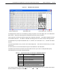
Hardware Specifications
Table 1-1.
Hardware
FP5 main unit
Hardware Specifications
Items
Specifications
Operating power supply
Supplied via AC adapter
Operating environment
Temperature: 0 to +40C
ccondition
Humidity: 10% to 80% RH (no condensation)
Storage environment
Temperature: 15 to +60C
ccondition
Humidity: 10% to 80% RH (no condensation)
Package size
140 90 30 mm (not including projections)
Weight
Approximately 230 g
Internal flash memory
Program file save area (16 MB)
Other (PR5 file save area, ESF file save area, firmware area, and FPGA area)
AC adapter
Operation mode
Programming GUI operation, standalone operation, remote operation, terminal operation
Specifications
AC input range:
100 to 240 V, 50/60 Hz
DC output:
15 V
Current consumption:
1 A (max.)
Host machine
Target host machine
PC98-NX series, IBM PC/AT compatible
interface
Target OS
Windows 2000, Windows XP
USB connector
Type A, USB 2.0 (compatible with 1.1)
USB cable
Approximately 2 m
Serial connector
9-pin D-SUB male connector for RS-232C @ 9600, 19200, 38400, 57600, 115200 bps
Serial cable
Approximately 3 m (cross cable)
Target connector
Connector:
15-pin HD-SUB female connector
Protected function:
Internal overvoltage input protection circuit
Target
interface
Note 1
Supported communication mode and rate:
3-wire serial I/O (CSI) (5.0 MHz max.)
3-wire serial I/O with handshake (CSI + HS) (5.0 MHz max.)
Pseudo 3-wire I/O (2.0 kHz max.)
UART (1 Mbps max.)
2
I C (100 kHz max.)
Target cable
Cable length: Approximately 42 cm
FP5 side: 15-pin HD-SUB male connector
Target system side: 16-pin 2.54 mm pitch multipurpose female connector
Note 2
Power supply
Target VDD power supply: 1.5 to 6.0 V, max. 200 mA
Internal overcurrent detection circuit
Power supply detection
Available. Current consumption: 1 mA or less
CPU clock supply
1 MHz, 2 MHz, 4 MHz, 5 MHz, 6 MHz, 8 MHz, 9 MHz, 10 MHz, 12 MHz, 16 MHz, 20 MHz
GND cable
Approximately 1 m
Notes 1. The maximum communication speed in the interface may vary depending on the device and environment
used.
2. VDD for the target system is supplied for the purpose of supplying power to the target device through
which writing is performed, so the specification cannot secure sufficient capacity to operate the target
system.
Use the power source on the target system when performing on-board programming.
Flash Memory Programmer FL-PR5 User’s Manual (Provisional)
SBA1-070002-00
14/138
CHAPTER 2 HARDWARE CONFIGURATION
This chapter explains the following items for hardware configuration.
Package contents
System configuration
2.1
Package Contents
Please verify that you have received all the parts listed in the package contents list included with the FP5 package.
If any part is missing or seems to be damaged, please contact an NEC Electronics sales representative or
distributor.
2.2
System Configuration
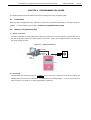
The FP5 system configuration is as shown in the diagram below.
Figure 2-1.
FP5 System Configuration
Serial cable
or
USB cable
AC adapter
Host machine
FP5
Target cable
GND cable
Target system or Program adapter
Notes 1. The target system and program adapter are not included in the FP5 package.
2. The program adapter is a product of Naito Densei Machida Mfg. Co., Ltd.
The FP5 is connected to the host system via an RS-232C serial cable or a USB cable.
the target system via a target cable.
The FP5 is connected to
For details on the target cable specifications, refer to CHAPTER 7
CONNECTORS AND CABLES.
2.2.1
Host machine
A host machine is used to communicate with the FP5. Windows 2000 or Windows XP is required for using the
programming GUI.
The host machine must also be equipped with a serial port or a USB port.
Flash Memory Programmer FL-PR5 User’s Manual (Provisional)
2.2.2
SBA1-070002-00
15/138
Serial cable
Communication is established by using a serial cable to connect the host machine serial port and FP5 serial
connector (RS-232C cross cable) connection.
For details on the serial cable specifications, refer to CHAPTER
7 CONNECTORS AND CABLES.
2.2.3
USB cable
Communication is established by connecting the host machine USB port and the FP5 USB connector (mini-B
type) using a USB cable.
For details on the USB cable specifications, refer to CHAPTER 7 CONNECTORS
AND CABLES.
2.2.4
AC adapter
Connect the FP5 power supply connector to the AC adapter included with the FP5.
adapter specifications, refer to 1.6
For details on the AC
Hardware Specifications.
Caution The AC adapter is exclusively for the FP5, so do not use it for other products.
2.2.5
Target cable
A 16-pin connector is equipped on the tip of the target cable, which is connected to the target system or the
program adapter.
For details on the target cable specifications, refer to CHAPTER 7 CONNECTORS AND
CABLES.
2.2.6
GND cable
To reinforce the GND, use a GND cable to connect the FP5 GND connector and the signal GND of the target
system or program adapter. For details on the GND cable specifications, refer to CHAPTER 7 CONNECTORS
AND CABLES.
Caution The FP5 and target system may be damaged if the voltage between the FP5 GND and the
target system GND is different.
Use the GND cable to match the voltage before connecting
the target cable.
2.2.7
Target system
The target system must be equipped with a device interface that complies with the target cable specifications.
For details on the specifications, refer to CHAPTER 7 CONNECTORS AND CABLES, CHAPTER 8 NOTES ON
TARGET SYSTEM DESIGN, and CHAPTER 9 SPECIFICATIONS OF TARGET INTERFACE CIRCUITS.
2.2.8
Program adapter
The FP5 supports off-board programming through which programs are written via a program adapter (FA series)
without mounting the target device onto the target system.
the target device package are available.
Program adapters corresponding to each type of
Flash Memory Programmer FL-PR5 User’s Manual (Provisional)
2.3
SBA1-070002-00
16/138
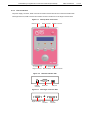
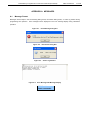
Names and Functions on Main Unit
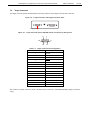
This section describes the names and functions on the FP5 main unit.
2.3.1
FP5 control panel
Indicators and buttons are laid out on the FP5 top.
Figure 2-2.
FP5 Top View <Control Panel>
POWER LED
POWER
button
Message display
Status LEDs
Control buttons
(1) Indicators
POWER LED
LED that displays the FP5 power status.
A red LED is turned on when the FP5 is ON, and is turned off when the FP5 is OFF.
Message display
An LCD display of 16 2-characters that indicates the operating mode or menus.
It is mainly used when the FP5 operates in standalone mode.
Status LEDs
LEDs that show the FP5 operating status.
PASS (green LED turned on) indicates normal completion, BUSY (orange LED flashes)
indicates processing in progress, and ERROR (red LED turned on) indicates errors.
(2) Buttons
POWER
button
Used to turn on/off the power to the FP5.
Press this button longer (for about 1 minute)
when turning off.
NEXT
ENTER
CANCEL
button
button
button
Proceeds to the next menu item at the same level in sequence.
Selects the item shown in the message display.
Cancels the current selection and returns to the previous menu item.
The command
currently running cannot be stopped, except for the [Read] command.
START
Remark
button
The
NEXT ,
Executes the [Autoprocedure(E.P.)] command.
ENTER ,
CANCEL
and
START
buttons are mainly used in standalone mode.
Flash Memory Programmer FL-PR5 User’s Manual (Provisional)
2.3.2
SBA1-070002-00
FP5 connectors
The power supply connector, serial connector and USB connector are laid out on the host interface side.
The target connector, GND connector and remote connector are laid out on the target connector side.
Figure 2-3.
FP5 Top View <Connector>
USB connector
Serial connector
Target connector
Figure 2-4.
Remote connector
FP5 Host Interface Side
Serial port
POWER
connector
Figure 2-5.
GND connector
POWER connector
USB port
FP5 Target Connector Side
Target connector
GND
connector
Remote
connector
17/138
Flash Memory Programmer FL-PR5 User’s Manual (Provisional)
SBA1-070002-00
18/138
(1) Power supply connector
Connect the power supply connector to the AC adapter included with the FP5.
For details on the power
supply connector specifications, refer to CHAPTER 7 CONNECTORS AND CABLES.
Caution Do not use an AC adapter other than that included with the FP5.
(2) Serial connector
Communication is established by using a serial cable (RS-232C cross cable) connection to connect the host
machine serial port and FP5 serial connector.
The data transfer conditions are as follows.
Data transfer speed: 9,600 bps, 19,200 bps, 38,400 bps, 57,600 bps, or 115,200 bps
Data bit: 8 bits
Parity: none
Stop bit: 1 bit
Flow control: hardware
The transfer speed is set to 115,200 bps by default, but it can be changed.
specifications, refer to CHAPTER 7
For details on the serial connector
CONNECTORS AND CABLES.
(3) USB connector
Communication is established by using a USB cable to connect the host machine USB port and the FP5 USB
connector (mini-B type).
This connector conforms with USB 2.0 standards.
connector specifications, refer to CHAPTER 7
For details on the USB
CONNECTORS AND CABLES.
(4) Target connector
Connect the target connector to the target system using the target cable for on-board programming.
the target connector to the program adapter using the target cable for off-board programming.
the target connector specifications, refer to CHAPTER 7
Connect
For details on
CONNECTORS AND CABLES.
(5) GND connector
To reinforce the GND, connect the FP5 GND connector and the signal GND of the target system or program
adapter using a GND cable.
For details on the GND connector specifications, refer to CHAPTER 7
CONNECTORS AND CABLES.
Caution The FP5 and target system may be damaged if the voltage between the FP5 GND and the
target system GND is different.
the target cable.
Use the GND cable to match the voltage before connecting
Flash Memory Programmer FL-PR5 User’s Manual (Provisional)
SBA1-070002-00
19/138
CHAPTER 3 SOFTWARE INSTALLATION
This chapter explains the following items related to installation.
Obtaining software
Installation
Uninstallation
Updating programming GUI, firmware and FPGA
3.1
Obtaining Software
Download the programming GUI, USB driver, and PG-FP5 parameter file (PR5 file) from the following website.
<Programming GUI (including USB driver)>
URL: http://www.ndk-m.cp.jp/asmis/ Click “FL-PR5”.
<PR5 file>
URLs Japanese version: http://www.necel.com/micro/ods/jpn/
English version:
http://www.necel.com/micro/ods/eng/ Click “Version-up Service”.
Select the micro controller to be used in the Each Device Series column and select the device name in the
Device Name column; the parameter file for PG-FP5 can then be found.
Caution Use of the latest version of software is recommended to assure the FP5 operation.
3.2
Installation
This section explains the installation procedure for the programming GUI, USB driver and parameter file (PR5 file).
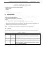
Table 3-1.
Installation Order
1
Installation
Item
Method
Programming
Run the downloaded self-extracting file (fp5guixxx.exe). An executable file (setup.exe) is
GUI
decompressed into the folder, so run it. And perform installation, following the directions on
the installer screen.
2
PR5 file
Run the downloaded self-extracting file (pr5xxxxxxx_vxxx.exe). A *.pr5 file is decompressed
into the folder, so copy it to the FP5_PRJ folder where the programming GUI is installed.
3
USB driver
The USB driver must be installed when connecting the FP5 and the host machine via the
USB interface. The USB driver is stored into the driver folder in the folder where the
programming GUI is installed. The USB driver is installed by Plug and Play. For details,
refer to 3.2.1 Installation of USB driver.
Flash Memory Programmer FL-PR5 User’s Manual (Provisional)
SBA1-070002-00
20/138
The folder configuration after programming GUI installation is as follows.
C:\
Folder structure for which installation is specified
\Program Files
\FL-PR5
[fp5.exe]
Folder where programming GUI is stored
\FP5_PRJ
Folder where PR5 files and ESF files are stored
(nothing is stored immediately after installation)
\DRIVER
Folder where USB driver is stored
[fpusb.sys]
[fpusb98.sys]
[fpusb.inf]
3.2.1
Installation of USB driver
The USB driver must be installed after installation of the programming GUI when connecting the FP5 and the
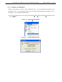
host machine via the USB interface. When the FP5 is connected to the USB port on the host machine for the
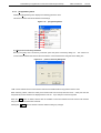
first time, the operating system automatically detects the FP5 by Plug and Play and the Welcome to the “Found
New Hardware Wizard” will start.
In this section, displays of Windows XP are used for explanation. Displays are different when using Windows
2000, but installation can be performed in the same manner.
(1) Start up the host machine.
(2) Use a USB cable to connect the FP5 to the host machine, plug in the AC adapter and the AC adapter to the
FP5 power supply connector.
(3) Press the
POWER
button on the FP5; the POWER LED will then turn on and “Command
displayed in the message display.
(4) The following window appears.
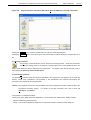
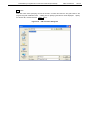
Select “No, not this time” and click the
Next >
button.
>” is
Flash Memory Programmer FL-PR5 User’s Manual (Provisional)
Figure 3-1.
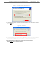
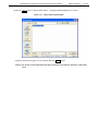
(5) The following window appears.
the
Next >
SBA1-070002-00
Found New Hardware Wizard Window <1>
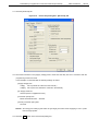
Select “Install from a list of specific location (Advanced)” and click
button.
Figure 3-2.
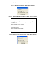
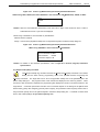
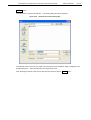
(6) The following window appears.
Found New Hardware Wizard Window <2>
Select “Search for the best driver in these locations”, “Include this location
in the search”, specify the folder where the USB driver is stored, and then click the
Remark
21/138
Next >
button.
When the Programming GUI is installed, the USB driver is installed into the driver folder in the
Programming GUI installation folder. “C:\Program Files\FL-PR5\driver” should usually be
specified.
The version indicates the version of the programming GUI. Specify the driver folder
for the latest programming GUI.
Flash Memory Programmer FL-PR5 User’s Manual (Provisional)
Figure 3-3.
SBA1-070002-00
22/138
Found New Hardware Wizard Window <3>
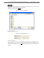
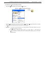
(7) If the following window appears, specify the same folder as specified in (6) for “Copy files from” and then
click the
OK
button.
Figure 3-4.
Files Needed
(8) If the message “Software has not passed Windows Logo testing” or “Windows can't verify the publisher of
this driver software” is displayed, select “Continue Anyway” or “Install this driver software anyway”.
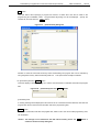
(9) The USB driver will then be installed, the FP5 is ready to communicate via the USB port.
Click the
Finish
button to complete the installation.
Flash Memory Programmer FL-PR5 User’s Manual (Provisional)
Figure 3-5.
Found New Hardware Wizard Window <4>
SBA1-070002-00
23/138
Flash Memory Programmer FL-PR5 User’s Manual (Provisional)
3.3
SBA1-070002-00
24/138
Uninstallation
This section explains how to uninstall the programming GUI, USB driver, parameter file (PR5 file), customized setup
file (ESF file) and setting information file (INI file). The uninstallation order is prescribed.
Table 3-2.
Uninstallation
Item
Method
Programming GUI
Open [Add or Remove Programs] (or [Add/ Remove Programs]) on the Control Panel and uninstall this
program. Parameter files (*.pr5), customized setup files (*.esf), files that contains programming GUI settings
contents (FP5.ini) are not deleted.
PR5 file
Delete PR5 files (*.pr5) stored in the FP5_PRJ folder in the programming GUI installation folder.
USB driver
Uninstall the USB driver using the device manager in the [System] menu on Control Panel. For details, refer
to 3.3.1 Uninstallation of USB driver.
ESF file
Delete ESF files (*.esf) stored in the FP5_PRJ folder in the programming GUI installation folder, or other folder.
INI file
Delete INI files (FP5.ini) stored in the WINDOWS folder.
3.3.1
Uninstallation of USB driver
Uninstall the USB driver, using the following procedure.
(1)
Start up the host machine.
(2)
Use a USB cable to connect the FP5 to the host machine, plug in the AC adapter and the AC adapter to
the FP5 power supply connector.
(3)
Press the
POWER
button on the FP5; the POWER LED will then turn on and “Command
>” is
displayed in the message display.
(4)
Open the Control Panel, double-click [System], click the [Hardware] tab, and the [Device Manager] button,
select [Flash Programmer FP5] under [NECPCIF] and then click the [Delete] icon on the toolbar.
(5)
Press the
POWER
button on the FP5 to turn power off; the POWER LED will then turn off. With this
method, device information in the registry is deleted but the copied files remain.
To completely delete all
of this information, perform the above step (4), refer to the list of files copied during installation and delete
the files.
This method requires special attention because it directly deletes files manage by Windows.
C:\WINDOWS\System32\Drivers\ fpusb.sys:
USB driver entity
C:\WINDOWS\inf\OemX.inf:
fpusb.inf
Caution The C:\WINDOWS\inf folder can be seen only when “Display all file and folder” is selected on
the [Display detail setting] tab in the folder option.
"X" in OemX.inf indicates a numeric value
starting from 0, which is assigned by the system.
The detailed contents of the OemX.inf file
must be checked.
The relevant file includes the following notation.
; Installation inf for the NEC Electronics Flash Programmer
;
; Copyright(C) NEC Electronics Corporation 2005
Flash Memory Programmer FL-PR5 User’s Manual (Provisional)
3.4
SBA1-070002-00
25/138
Updating Programming GUI, Firmware and FPGA
The firmware and FPGA are programs embedded in the device for controlling the FP5. Updating the programming
GUI, firmware and FPGA enables the following.
Addition of newly supported functions or devices
Correction of restrictions
Use of the latest versions of the programming GUI, firmware and FPGA are recommended to assure the FP5
operation.
The latest versions are available on the following website.
Website
http://www.ndk-m.co.jp/asmis/
Caution If update of firmware and FPGA is improperly performed, FP5 may no longer operate.
Refer to the
following procedure or method for updating.
Remark PR5 files, ESF files and program files are not changed, even if firmware and FPGA are updated.
Be sure to follow the procedure below when updating the firmware and FPGA.
Step 1. Check the current version. (Refer to 3.4.1 Checking the current version.)
Step 2. If not the latest version, update the programming GUI. (Refer to 3.4.2 Installation of programming GUI.)
Step 3. Update the firmware using the latest programming GUI. (Refer to 3.4.3 Installation of firmware update.)
Step 4. Update the FPGA using the programming GUI. (Refer to 3.4.4 Installation of FPGA update.)
Flash Memory Programmer FL-PR5 User’s Manual (Provisional)
3.4.1
SBA1-070002-00
26/138
Checking the current version
(1)
Open the main window of the programming GUI. (Refer to 4.1 Introduction.)
(2)
Check the versions of the programming GUI, firmware and FPGA, as shown below.
Programming GUI: [Help] menu [About]
Firmware:
[Programmer] menu [Reset] command
Note
FPGA:
[Programmer] menu [Reset] command
Note
Note
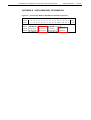
Display example of [Reset] command
>ver
Firmware Version V1.00
Board H/W V1,
FPGA V1
Firmware version
FPGA version
Serial No.: XXXXXXXXXX
>
(3)
The latest versions are available on the following websites.
Website
http://www.ndk-m.co.jp/asmis/
3.4.2
Installation of programming GUI
Run the downloaded self-extracting file (fp5guixxx.exe). An executable file (setup.exe) is decompressed into the folder, so run
it. And perform installation, following the directions on the installer screen.
Flash Memory Programmer FL-PR5 User’s Manual (Provisional)
3.4.3
27/138
Installation of firmware update
Install the latest firmware by using the latest programming GUI.
(fp5_fw_vxxx.exe).
folder.
SBA1-070002-00
Run the downloaded self-extracting file
Firmware file “fp5_fw_vxxx.rec” will then be decompressed into the folder, so copy it to any
(“xxx” indicates the firmware version.)
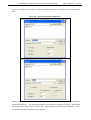
(1) Click the [Programmer] menu on the menu bar and select [Update Firmware]; the [Update Firmware] dialog
box will then be opened.
Figure 3-6.
[Update Firmware] Command
Figure 3-7.
[Update Firmware] Dialog Box
Flash Memory Programmer FL-PR5 User’s Manual (Provisional)
(2) Click the
OK
button to continue firmware update.
Figure 3-8.
SBA1-070002-00
28/138
The [Open firmware file] dialog box is opened.
[Open firmware file] Dialog Box
Select the firmware file “fp5_fw_vxxx.rec” and then click the
Open
button.
Caution Do not use FP5 firmware other than the one posted on the website; otherwise, a defect may
occur.
Flash Memory Programmer FL-PR5 User’s Manual (Provisional)
SBA1-070002-00
29/138
(3) Some commands are sent to the FP5 and the update progress status is displayed in the action log window.
The message “Firmware Update succeeds”, which indicates normal completion of firmware update, and
“Restarting FP5..”, which is equivalent to [RESET] command processing, is automatically performed.
new version can then be checked as “Firmware Version Vx.xx”.
Remark
The
The update takes about 10 seconds.
The action log window is a part of the main window of the programming GUI, which shows the
operation progress status.
Figure 3-9.
Action Log Window When Firmware Update Is Finished
Flash Memory Programmer FL-PR5 User’s Manual (Provisional)
3.4.4
SBA1-070002-00
30/138
Installation of FPGA update
Install the latest FPGA by using the latest programming GUI.
(fp5_fpga_vxxx.exe).
to any folder.
Run the downloaded self-extracting file
The FPGA file “fp5_fpga_vxxx.rec” will then be decompressed into the folder, so copy it
(“xxx” indicates the FPGA version.)
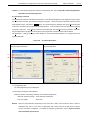
(1) Click the [Programmer] menu on the menu bar and select [Update FPGA]; the [Update FPGA] dialog box will
then be opened.
Figure 3-10.
[Update FPGA] Command
Figure 3-11.
[Update FPGA] Dialog Box
Flash Memory Programmer FL-PR5 User’s Manual (Provisional)
(2) Click the
OK
button to continue FPGA update.
Figure 3-12.
SBA1-070002-00
31/138
The [Open FPGA file] dialog box is opened.
[Open FPGA file] Dialog Box
Select the FPGA file “fp5_fpga_vxxx.rec” and then click the
Open
button.
Caution Do not use an FP5 FPGA other than the one posted on the website; otherwise, a defect may
occur.
Flash Memory Programmer FL-PR5 User’s Manual (Provisional)
SBA1-070002-00
32/138
(3) Some commands are sent to the FP5 and the update progress status is displayed in the action log window.
The message “Result pass” , which indicates normal completion of firmware update, and “FP5 Power will be
switched OFF now.....”, which is equivalent to processing when the
automatically executed.
OK
turn on power.
button is turned off, is
The update takes about 30 seconds.
Figure 3-13.
(4) Click the
POWER
Action Log Window When FPGA Update Is Finished
button in the error message dialog box and then press the
POWER
button on the FP5 to
Flash Memory Programmer FL-PR5 User’s Manual (Provisional)
SBA1-070002-00
33/138
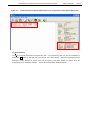
(5) Click the [Programmer] menu on the menu bar and select [Setup host connection...]; the [Host Connection]
dialog box will then be opened.
Select the communication mode used and then click the
Figure 3-14.
[Setup host connection] Command
Figure 3-15.
[Host Connection] Dialog Box
OK
button.
Flash Memory Programmer FL-PR5 User’s Manual (Provisional)
(6) Communication with the host machine is established.
SBA1-070002-00
“Board H/W V1, FPGA V1” is displayed in the action
log window; thus, the version can be checked.
Figure 3-16.
34/138
Version Confirmation After FPGA Update Is Finished
Flash Memory Programmer FL-PR5 User’s Manual (Provisional)
SBA1-070002-00
35/138
CHAPTER 4 PROGRAMMING GUI USAGE
This chapter explains functional details on windows and dialog boxes of the programming GUI.
4.1
Introduction
Make sure that the programming GUI, USB driver, and the FP5 parameter file (PR5 file) for the target device are
installed.
4.2
For the installation method, refer to CHAPTER 3 SOFTWARE INSTALLATION.
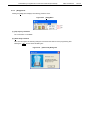
Startup of Programming GUI
(1) System connection
Connect a USB cable (or serial cable) to the USB port (or serial port) on the host machine, and the other side of
the cable to the USB connector (or serial connector) on the FP5.
Plug in the AC adapter and then connect to the
FP5 power supply connector.
Figure 4-1.
System Connection
Serial cable
or
USB cable
AC adapter
Host
machine
Outlet
FP5
(2) FP5 startup
After the cables are connected, press the
POWER LED is turned on and “Commands
POWER
button on the FP5. When the FP5 is correctly started, the
>” is displayed in the message display.
defect in the FP5, so consult an our sales representative or distributor.
If not, the cause may be a
Flash Memory Programmer FL-PR5 User’s Manual (Provisional)
SBA1-070002-00
36/138
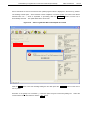
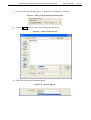
(3) Startup of programming GUI
Click the Start menu, “All Programs”, point to “FL-PR5” and then select “FL-PR5” to start the Programming GUI.
The valid communication mode is automatically detected in the order of the USB, and then the serial interface.
Figure 4-2.
Port Scanning at Startup of Programming GUI
The communication mode can also be selected by cancelling this operation by clicking the
Cancel
button and
selecting the [Setup host connection...] command in the [Programmer] menu.
When communication is established and the programming GUI is correctly started, the main window will be
opened.
The following message will be displayed if the programming GUI is started for the first time or valid
programming areas have been cleared, so click the
Figure 4-3.
OK
button.
Message Displayed at the First Startup of Programming GUI
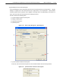
The Device Setup dialog box, which is usually opened by executing the [Setup...] command in the [Device] menu,
will open.
Perform settings in this dialog box.
For the setting method, refer to 4.3.3 (12) [Setup...] command.
Flash Memory Programmer FL-PR5 User’s Manual (Provisional)
Figure 4-4.
SBA1-070002-00
37/138
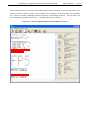
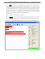
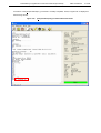
Main Window
<1> Menu bar
<4> Programmer parameter window
<2> Toolbar
<3> Action log window
<6> Hint bar
<5> Status bar
The main window consists of the following areas.
Name
Displayed Items
Refer to:
<1>
Menu bar
Menu items executable by the programming GUI
4.3
<2>
Toolbar
Frequently used commands, as buttons
4.4
<3>
Action log window
A programming GUI action log
4.5
<4>
Programming parameter window
Programming parameter settings
4.6
<5>
Status bar
Command progress shown as a color or with a message
4.7
<6>
Hint bar
Hints for commands and toolbar
4.8
Flash Memory Programmer FL-PR5 User’s Manual (Provisional)
4.3
SBA1-070002-00
38/138
Menu Bar
The menu bar displays the commands that are available for the programming GUI. Some commands may be
unavailable when the programming GUI is started for the first time, or depending on the parameter file (PR5 file)
selected.
Caution During command execution, do not execute other commands or terminate the programming GUI.
4.3.1
[File] menu
The following pull-down menu appears by clicking the [File] menu.
This menu includes commands related to program file operation.
Figure 4-5. [File] Menu
(1)
(2)
(3)
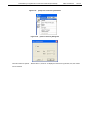
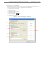
(1) [Hex Editor...] command
The [Hex Editor] menu allows you to edit a program file in Intel HEX format or Motorola HEX format.
When this command is executed, a HEX Editor select dialog box is opened and the file to be edited
can be specified.
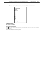
Figure 4-6.
HEX Editor Select Dialog Box
HEX Files (*.HEX), SREC Files (*.REC) or All files (*.*) may be selected from the Files of types list box.
After selecting a file to be opened, the file selected in the HEX Editor main window is loaded.
At this time,
whether the file is of the Intel HEX format or Motorola HEX format is automatically recognized. When loading is
finished, the HEX Editor main window is opened.
Flash Memory Programmer FL-PR5 User’s Manual (Provisional)
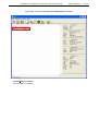
Figure 4-7.
39/138
HEX Editor Main Window
Data display area
Address display area
SBA1-070002-00
ASCII display area ID Tag area
The displayed file contents can be modified by placing the pointer in the data display area in the HEX Editor
main window.
Data input via the keyboard is accepted for all shown memory locations.
The ID Tag area is the area used with the target device supporting data flash.
can be edited in this area.
Only address 400000h and later
For details on data flash and ID tags, refer to the user’s manual of the target device.
The HEX Editor only accepts hexadecimal data, i.e., numbers 0 to 9 and letters A to F. All other data will be
rejected.
The ASCII representation, if any, is shown in the ASCII display area.
This area is for reference only, so no data
can be input.
Use the scroll bar to move another address range into the visible area of the HEX Editor.
The address space that can be viewed in the HEX Editor window is up to 4 MB + 64 KB (data flash space).
The following keys can be input using the keyboard.
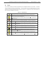
Table 4-1.
Key Functions That Can Be Input in HEX Editor Window
Key
0-9, A-F
Function
Data input (data display area)
Move cursor in right direction
Move cursor in left direction
Move cursor in up direction
Move cursor in down direction
Tab Move cursor to next input field (address + 1)
If any change has been made to the file, [Save] and [Save As] in the [File] menu in the HEX Editor main window
become available for saving the modified data.
Flash Memory Programmer FL-PR5 User’s Manual (Provisional)
SBA1-070002-00
40/138
The [Save As] display varies whether or not the downloaded PR5 file is for the target device that supports data
flash.
Figure 4-8.
[Save As] Dialog Box of HEX Editor
The downloaded PR5 file is for a target device that does not support data flash
The downloaded PR5 file is for a target device that supports data flash
Besides the file name and folder location, a start address and an end address for the new file can be selected in
the [Save As] dialog box.
The original start address and end address are displayed by default.
radio button for the format in which to save the data.
the saved file with other tool products is not supported.
Select the file
Select the same format as that of the loaded file.
Use of
Flash Memory Programmer FL-PR5 User’s Manual (Provisional)
SBA1-070002-00
41/138
Remark For the saved program file contents of the data flash area, refer to Figure B-1 Relationship Between
HEX Editor and Saved Program File.
(2) [Checksum] command
The [Checksum] command calculates the checksum of the selected program file and displays the result. When
this command is executed, the Checksum dialog box appears.
target address range, and click the
OK
button. The result will then be displayed in the [File Checksum] area
in the action log window and programmer parameter window.
command is executed.
Select the optional calculation method and the
This command can be executed after the [Setup]
If the [Setup] command is executed again after the [Checksum] command is executed,
the result displayed in the [File Checksum] area in the programmer parameter window will be cleared.
The [Checksum...] dialog box display varies whether or not the downloaded PR5 file is for a target device that
supports data flash.
Figure 4-9.
Checksum Dialog Box
The downloaded PR5 file is for a target device that
The downloaded PR5 file is for a target device that
does not support data flash
supports data flash
<1>
<1>
<2>
<2>
<3>
<3>
<1> Programming area
The valid programming area is displayed.
<2> Checksum calculation mode selection
Select the mode for calculating checksum of the selected program file.
Arithmetic checksum (16bit): 16-bit arithmetic (subtraction)
CRC sum (32bit):
Remark
32-bit CRC
With the 16-bit arithmetic (subtraction) mode, the lower 4 digits of the result from which a value is
subtracted from 00h in 1-byte units are displayed. With 32-bit mode, the 8-digit result of CRC32
function calculation is displayed.
CRC Calculation Specifications.
For details on arithmetic specifications, refer to Figure B-2 32-bit
Flash Memory Programmer FL-PR5 User’s Manual (Provisional)
SBA1-070002-00
42/138
<3> Address range selection
Select the range for calculating checksum of the selected program file.
If there is no program file data in the
specified range, the specified range is filled with FFh for calculation.
Device Area:
From the start to end addresses of the device, which are contained in the selected PR5 file
User Defined: Any range can be specified by inputting the addresses to the [Start Address] and [End
Address] text boxes.
Clicking the
OK
button displays the calculation result in the [File Checksum] area in the action log window
and programmer parameter window.
Clicking the
Cancel
button closes the dialog box without saving the settings made in the Checksum dialog
box.
Remark When the valid programming area is changed or a program file is downloaded, the checksum result will
be cleared.
Figure 4-10. Checksum Result <If Downloaded PR5 File Is for Target Device That Does Not Support Data Flash>
Flash Memory Programmer FL-PR5 User’s Manual (Provisional)
Figure 4-11.
SBA1-070002-00
43/138
Checksum Result <If Downloaded PR5 File Is for Target Device That Supports Data Flash>
(3) [Quit] command
The [Quit] command terminates the programming GUI.
clicking the
The programming GUI can also be terminated by
button on the right end of the title bar in the main window. When the programming GUI is
terminated, various settings are saved in the INI file (FP5.ini), and these settings are loaded when the
programming GUI is started the next time.
The INI file is created in the WINDOWS folder.
Flash Memory Programmer FL-PR5 User’s Manual (Provisional)
4.3.2
SBA1-070002-00
44/138
[Programmer] menu
Clicking the [Programmer] menu displays the following pull-down menu.
This menu includes commands related to FP5 settings.
Figure 4-12.
[Programmer] Menu
(1)
(2)
(3)
(4)
(5)
(6)
(7)
(8)
(9)
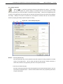
(1) [Setup host connection] command
Running the [Setup host connection] command opens the [Host Connection] dialog box.
The channel for
communication between the FP5 and the host machine can be selected and configured in this dialog box.
Figure 4-13.
[Host Connection] Dialog Box
“USB” can be selected as the communication channel if the USB interface is supported in the PC used.
When selecting “Serial”, select the COM port and baud rate from the drop-down list boxes.
recognized by the host machine are displayed in the Port list.
When the
OK
Up to 256 ports can be recognized.
button is clicked, software tries to establish a connection between the FP5 and the host machine
using the selected communication channels.
Clicking the
COM ports that are
Cancel
button closes the window without making any changes.
Flash Memory Programmer FL-PR5 User’s Manual (Provisional)
SBA1-070002-00
45/138
(2) [Logging] command
The [Logging] command saves information displayed in the action log window in the log file.
When this
command is executed, the log file save dialog box appears. Move to an arbitrary folder, select the log file in the
[File name] drop-down list, and click the
Save
command on the menu bar will be checked.
The check mark will be cleared by clicking the [Logging] command
again and saving of the log file will be stopped.
stamp.
Remark
button; the log file will then be saved.
Enabling/disabling the [Logging] command is added to the time
For a log file example, refer to Figure B-3 Log File Example.
The log file that was saved the last time is displayed in the log file save dialog box.
Figure 4-14.
Clicking the
Save
Clicking the
Cancel
The [Logging]
Log File Save Dialog Box
button saves the specified log file.
button closes the dialog box without saving the log file.
Flash Memory Programmer FL-PR5 User’s Manual (Provisional)
SBA1-070002-00
46/138
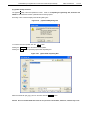
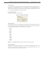
(3) [Select Programming area] command
The FP5 has a 16 MB flash memory area for saving program files.
This memory area can be used
as four 4 MB programming areas (Area 0 to Area 3) or eight independent 2 MB programming areas
(Area 0 to Area 7).
Program files can be downloaded to each programming area, and which file, PR5 or ESF,
is to be saved is selectable in programming area units.
That is, files can be individually downloaded in each
programming area, and the area used can also be selected individually.
This command is used to select a valid programming area from the FP5’s four (or eight) programming areas (4
MB in case of four areas, or 2 MB in case of eight areas). When this command is executed, the programming
area select dialog box is opened, and the desired programming area can be selected.
The number of
programming areas that can be selected with this command is the value defined in the [Programming Area
Setting] area on the [Target] tab of the Device Setup dialog box, which is opened by the [Setup...] command in
the [Device] menu.
Figure 4-15.
Programming Area Select Dialog Box
The currently selected programming area is displayed in the programming area selection dialog box.
change the area, select the relevant number from the list box and click the
OK
button.
To
To check the
contents set to each area or to change the division factor, see the [Target] tab of the Device Setup dialog box.
Clicking the
OK
button selects the programming area selected in the programming area select dialog box.
Clicking the
Cancel
button closes the dialog box without changing the programming area.
(4) [Buzzer] command
The [Buzzer] command is used to enable or disable the setting to output the buzzer sound from the FP5 main
unit. When this command is executed, the [Buzzer] command on the menu bar is checked and becomes valid.
When this command is executed again, the check mark is cleared and the command becomes invalid.
The
FP5 makes a double-beep sound when the Autoprocedure(E.P.) command is completed normally, or makes a
buzzer sound when the command results in an error.
(5) [Reset] command
When the [Reset] command is executed, a software reset can be applied to the FP5. After reset, the current
versions of the firmware and FPGA, and the FP5 serial number will be displayed in the action log window.
Flash Memory Programmer FL-PR5 User’s Manual (Provisional)
SBA1-070002-00
47/138
(6) [Self-Test] command
The [Self-Test] command executes the FP5 self-testing program.
self-testing.
The following four items are subject to
The self-testing program does not affect the PR5 files, ESF files and program files saved in the
FP5.
<1> FPGA test
<2> Power generation block test
<3> Target interface I/O test
<4> Remote interface I/O test
Since execution of the [Self-Test] command involves I/O testing, a message that prompts the user to disconnect
hardware connected the target connector or remote connector is displayed.
Remove hardware (including
target system and program adapter), connected to the target connector or remote connector, if any.
that no hardware is connected and click the
If the
Cancel
OK
Make sure
button; self-testing will then be executed.
button is clicked, self-testing will not be executed.
Figure 4-16.
Confirmation Before Starting Self-Testing
Self-testing takes about three seconds, and the result will be displayed in the action log window and a result dialog
box.
If the message “Selftest FAILED.” is displayed, the cause may be a defect in the FP5, so consult an NEC
Electronics sales representative or distributor.
Figure 4-17.
When Self-Testing Result Is “PASSES” <Action Log Window>
>selftest
***** CAUTION *****
Remove any plugs from Target- and Remote-Connector before starting.
Any hardware attached to those connectors may be damaged by this test !
***** CAUTION *****
Target- and Remote-connector unplugged ?
If yes, press 's' to start the test: s
FPGA Test: PASS
Power Supply Test: PASS
Target- and Remote-Interface Test: PASS
Selftest PASSED.
>
Flash Memory Programmer FL-PR5 User’s Manual (Provisional)
Figure 4-18.
Figure 4-19.
SBA1-070002-00
When Self-Testing Result Is “PASSES” <Result Dialog Box>
Example for When Self-Testing Result Is “FAILED” <Action Log Window>
>selftest
***** CAUTION *****
Remove any plugs from Target- and Remote-Connector before starting.
Any hardware attached to those connectors may be damaged by this test !
***** CAUTION *****
Target- and Remote-connector unplugged ?
If yes, press 's' to start the test: s
FPGA Test: PASS
Power Supply Test: PASS
Target- and Remote-Interface Test: FAIL
Selftest FAILED.
>
Figure 4-20.
Example for When Self-Testing Result Is “FAILED” <Result Dialog Box>
48/138
Flash Memory Programmer FL-PR5 User’s Manual (Provisional)
SBA1-070002-00
49/138
(7) [Update Firmware] command
The [Update Firmware] command updates the firmware.
Refer to 3.4 Updating Programming GUI, Firmware
and FPGA and download the relevant update file before starting update.
Executing of this command displays the following dialog box.
Figure 4-21.
To continue the firmware update, click the
Clicking the
Cancel
Clicking the
OK
[Update Firmware] Dialog Box
OK
button.
button cancels the firmware update.
button opens the [Open firmware file] dialog box.
Figure 4-22.
[Open firmware file] Dialog Box
Select the firmware file “fp5_fw_vxxx.rec” and then click the
Open
button.
Caution Do not use FP5 firmware other than the one posted on the website; otherwise, a defect may
occur.
Flash Memory Programmer FL-PR5 User’s Manual (Provisional)
SBA1-070002-00
Some commands are sent to the FP5 and the update progress status is displayed in the action log window.
50/138
The
message “Firmware Update succeeds”, which indicates normal completion of firmware update, and “Restarting
FP5..”, which is equivalent to [RESET] command processing, is automatically performed.
then be checked as “Firmware Version Vx.xx”.
Figure 4-23.
The new version can
The update takes about 10 seconds.
Action Log Window When Firmware Update Is Finished
Flash Memory Programmer FL-PR5 User’s Manual (Provisional)
SBA1-070002-00
51/138
(8) [Update FPGA] command
The [Update FPGA] command updates the FPGA.
Refer to 3.4 Updating Programming GUI, Firmware and
FPGA and download the relevant update file before starting update.
Executing of this command displays the following dialog box.
Figure 4-24.
To continue the FPGA update, click the
Clicking the
Cancel
Clicking the
OK
OK
[Update FPGA] Dialog Box
button.
button cancels the FPGA update.
button opens the [Open FPGA file] dialog box.
Figure 4-25.
[Open FPGA file] Dialog Box
Select the FPGA file “fp5_fpga_vxxx.rec” and then click the
Open
button.
Caution Do not use FP5 FPGA other than the one posted on the website; otherwise, a defect may occur.
Flash Memory Programmer FL-PR5 User’s Manual (Provisional)
SBA1-070002-00
52/138
Some commands are sent to the FP5 and the update progress status is displayed in the action log window.
The message “Result pass” , which indicates normal completion of firmware update, and “FP5 Power will be
switched OFF now.....”, which is equivalent to processing when the
automatically executed.
OK
button is turned off, is
The update takes about 30 seconds.
Figure 4-26.
Click the
POWER
Action Log Window When FPGA Update Is Finished
button in the error message dialog box and then press the
POWER
button on the FP5 to
turn on power.
Execution of the [Setup host connection...] command opens the [Host Connection] dialog box.
communication mode used and then click the
OK
button.
Select the
Flash Memory Programmer FL-PR5 User’s Manual (Provisional)
Figure 4-27.
SBA1-070002-00
53/138
[Setup host connection] Command
Figure 4-28.
[Host Connection] Dialog Box
The main window is opened. “Board H/W V1, FPGA V1” is displayed in the action log window; thus, the version
can be checked.
Flash Memory Programmer FL-PR5 User’s Manual (Provisional)
Figure 4-29.
(9) [FP5 Manager] command
This command is not available.
SBA1-070002-00
Version Confirmation After FPGA Update Is Finished
54/138
Flash Memory Programmer FL-PR5 User’s Manual (Provisional)
4.3.3
SBA1-070002-00
55/138
[Device] menu
The following pull-down menu appears by clicking the [Device] menu.
This menu includes commands mainly related to programming to the target device, such as erase, write and
verify.
Figure 4-30.
[Device] Menu
(1)
(2)
(3)
(4)
(5)
(6)
(7)
(8)
(9)
(10)
(11)
(12)
(1) [Blank check] command
The [Blank Check] command performs blank check for the flash memory in the target device.
The
target area can be set in the [Operation Mode] area on the [Standard] tab in the Device Setup
dialog box.
If the flash memory has already been erased, “Blank check OK” is displayed.
has not yet been erased, “ERROR” is displayed.
If the flash memory
If this error is displayed, erase the entire area of the flash
memory before starting programming.
(2) [Erase] command
The [Erase] command erases the flash memory in the target device.
The target area can be set in
the [Operation Mode] area on the [Standard] tab in the Device Setup dialog box.
If this command
is executed with [Chip] selected, security command options are initialized at the same time. While erasing the
flash memory is in progress, the progress status is displayed in the action log window.
When execution of this
command is completed, the result of command execution in the target device is displayed. Whether to perform
the [Blank Check] command before executing this command depends on the [Blank check before Erase] check
box setting in the [Command options] area on the [Advanced] tab in the Device Setup dialog box.
If this
command is executed for the target device that has already been erased with the [Blank check before Erase]
check box selected, “OK, Erase skipped.” is displayed and erasure is not performed.
(3) [Program] command
The [Program] command transmits the memory contents (program files) in the FP5 valid
programming area to the target device and writes the programs to the flash memory.
The target
area can be set in the [Operation Mode] area on the [Standard] tab in the Device Setup dialog box.
progress status of this command is displayed as a percentage in the action log window.
The
When execution of this
command is completed, the programming GUI displays the result of command execution in the target device.
Command options after execution of this command depend on the settings of the [Verify after Program],
[Security after Program] and [Checksum after Program] check boxes in the [Command options] area on the
Flash Memory Programmer FL-PR5 User’s Manual (Provisional)
[Advanced] tab in the Device Setup dialog box.
SBA1-070002-00
56/138
For details on these check boxes, refer to 4.3.3 (12) (c) <2>
[Command options] area.
(4) [Verify] command
The [Verify] command transmits the memory contents (program files) in the FP5 valid programming
area to the target device, verifies the data written to the flash memory in the target device, and
receives the result.
The target area can be set in the [Operation Mode] area on the [Standard] tab in the
Device Setup dialog box.
The progress status of this command is displayed as a percentage in the action log
window. When execution of this command is completed, the programming GUI displays the result of command
execution in the target device.
(5) [Read] command
The [Read] command loads data on the flash memory in the target device and saves it as a file. When the
[View] command is executed following this command, 4 KB read data is displayed in the log window each time
the ENTER key is pressed. When the [Write Intel HEX file] or [Write Motorola SREC file] command is executed
following this command, the read data can be saved in the Intel HEX format or Motorola HEX format.
Use of
the saved file with other tool products is not supported.
Remark
The folder in which program data was saved the last time is displayed in the program data save
dialog box.
Caution The [Read] command is available only when using a single-power-supply flash memory
microcontroller that supports the [Read] command.
Figure 4-31.
Program Data Saved Dialog <When Write Intel HEX file Command Is Executed>
Flash Memory Programmer FL-PR5 User’s Manual (Provisional)
SBA1-070002-00
57/138
Figure 4-32.
Program Data Save Dialog Box <When Write Motorola SREC file Command Is Executed>
Clicking the
Open
Clicking the
Cancel
button saves the program data into a file and closes the dialog box.
button closes the program data save dialog box without saving the program data into a
file.
(6) [Security] command
The [Security] command sets the security functions for the target device. When this command is
executed, the settings made in the [Security command option] area on the [Advanced] tab in the
Device Setup dialog box will be reflected in the target device.
For details on the security functions, refer to
4.3.3 (12) (c) <3> [Security command option] area.
(7) [Checksum] command
The [Checksum] command reads the checksum calculated in the target device and displays it in the action log
window.
When using a 78K0S/Kx1+ microcontroller or the PD78F9334, this command also displays the
checksum of the program file and compares both.
Remark The checksum read by this command differs from the one displayed in the [File checksum] area in the
programmer parameter window.
For details on the [File checksum] area, refer to 4.3.1 (2)
[Checksum...] command.
The checksum is calculated as follows.
<When using 78K0, 78K0S (other than 78K0S/Kx1+ microcontrollers and PD78F9334), 78K0R, or V850>
Method: Subtraction (16-bit arithmetic)
Range: Area set in the [Operation Mode] area on the [Advanced] tab in the Device Setup dialog box
Flash Memory Programmer FL-PR5 User’s Manual (Provisional)
Figure 4-33.
SBA1-070002-00
58/138
Action Log Window After [Checksum] Command Execution
<When using 78K0, 78K0S (other than 78K0S/Kx1+ microcontrollers and PD78F9334), 78K0R, or V850>
>sum
0x623E
OK
>
Remark With the 16-bit arithmetic (subtraction) mode, the lower 4 digits of the result from which a value is
subtracted from 00h in 1-byte units are displayed.
<When using a 78K0S/Kx1+ microcontroller or PD78F9334>
Method: Division (original)
Range: Area set in the [Operation Mode] area on the [Advanced] tab in the Device Setup dialog box
Figure 4-34.
Action Log Window After [Checksum] Command Execution
<When using 78K0S/Kx1+ microcontroller or PD78F9334>
>sum
Device Checksum: 0x1842
FP5 Checksum:
0x1842
Checksum compare: OK
>
Remark For details on the arithmetic specifications, refer to Figure B-4
Division (Original) Calculation
Specifications.
(8) [Autoprocedure(E.P.)] command
The [Autoprocedure(E.P.)] command executes the [Erase] and [Program] commands in succession.
Exiting from the flash memory programming mode is not possible between the [Erase] and
[Program] commands.
The target area can be set in the [Operation Mode] area on the [Standard] tab in the
Device Setup dialog box.
The progress status of this command is displayed in the action log window. When
execution of this command is completed, the programming GUI displays the result of command execution in the
target device.
Command options after execution of this command depend on the settings of the [Blank check
before Erase], [Verify after Program], [Security after Program], and [Checksum after Program] check boxes in
the [Command options] area on the [Advanced] tab in the Device Setup dialog box.
boxes, refer to 4.3.3 (12) (c) <2> [Command options] area.
For details on these check
Flash Memory Programmer FL-PR5 User’s Manual (Provisional)
Figure 4-35.
SBA1-070002-00
59/138
Action Log Window After [Autoprocedure(E.P.)] Command Execution
>ep
Blank check Chip: OK
OK, Erase skipped.
Erase OK
Write Chip:
10%
20%
30%
40%
50%
60%
70%
80%
90%
100%
OK
Write OK
Erase, Program OK
>
(9) [Connect] command
This command is not available.
(10) [Signature read] command
The [Signature read] command reads target device product information, such as the device name and flash
memory information.
The read result is displayed in the action log window.
Flash Memory Programmer FL-PR5 User’s Manual (Provisional)
SBA1-070002-00
60/138
(11) [Get Security Settings] command
The [Get Security Settings] command reads the settings for the security functions for the target device and
displays the result in the [Security flag settings] area on the [Advanced] tab in the Device Setup dialog box.
When execution of this command is enabled, execute this command before the [Security] command; the settings
for the security functions or the boot area can thus be checked.
For details on the security functions, refer to
4.3.3 (12) (c) <3> [Security command option] area.
Figure 4-36.
[Get Security Settings] Command
Flash Memory Programmer FL-PR5 User’s Manual (Provisional)
SBA1-070002-00
61/138
(12) [Setup] command
When the [Setup...] command is executed, the Device Setup dialog box is opened. In this dialog
box, select a program file, perform settings in accordance with the user environment for flash
memory programming, set command options, and perform security settings.
Each time the programming GUI
is started, the programming GUI loads the PR5 file, ESF file and program file that were used last and displays
the settings.
Settings for the items not dimmed can be changed in accordance with the user environment.
Switch the [Target], [Standard] and [Advanced] tabs for setting.
Figure 4-37.
(a)
Remark
(b)
Device Setup Dialog Box
(c)
PR5 file (parameter file)
PR5 files (parameter files) contain parameter information required for writing programs to the flash
memory in the target device.
Do not change the PR5 file data because it affects assurance of
written data; otherwise, the programming GUI will not recognize the PR5 file.
ESF file (customized setup file)
ESF files (customized setup files) contain the programming environment settings specific to the user
environment and PR5 file names.
recognize the ESF file.
If the file contains invalid contents, the programming GUI will not
Flash Memory Programmer FL-PR5 User’s Manual (Provisional)
When the
OK
SBA1-070002-00
62/138
button (button common to [Target], [Standard] and [Advanced] tabs) is clicked, program areas
are cleared and PR5 files, ESF files and program files are downloaded for the FP5. After that, the settings
made on the [Target], [Standard] and [Advanced] tabs are saved into an ESF file.
to the programming parameter window.
These settings are reflected
If there are settings which have not been updated, the files related to
the settings are not downloaded. When a program file is downloaded, the date and checksum of that file are
displayed in the action log window.
specifications, refer to Figure B-2
The checksum is calculated as shown below.
For details of the arithmetic
32-bit CRC Calculation Specifications.
Method: 32-bit CRC
Range: From the start to end addresses in the program file
When the
Cancel
button (button common to [Target], [Standard] and [Advanced] tabs) is clicked, the dialog
box is closed without saving changed settings on the [Target], [Standard] and [Advanced] tabs into an ESF file.
Figure 4-38.
Clearing of Programming Area, PR5 Files and ESF Files, and Download of Program File
Flash Memory Programmer FL-PR5 User’s Manual (Provisional)
SBA1-070002-00
63/138
(a) [Target] tab in Device Setup dialog box
Settings related to programming areas, PR5 files, ESF files and program files can be performed on the
[Target] tab in the Device Setup dialog box.
This tab consists of the following items.
<1> [Programming Area Setting] area
<2> [Target Setting] area
<3> [Parameter and Setting file] area
<4> [Object HEX file] area
<5> [Information] area and
Clear
button
<6> Programming area map area
Figure 4-39.
Device Setup Dialog Box - [Target] Tab
<1>
<2>
<3>
<6>
<4>
<5>
Flash Memory Programmer FL-PR5 User’s Manual (Provisional)
SBA1-070002-00
64/138
<1> [Programming Area Setting] area
The FP5 has a 16 MB flash memory area for saving program files.
This memory area can be used as
four 4 MB programming areas (Area 0 to Area 3) or eight independent 2 MB programming areas (Area 0
to Area 7).
Program files can be downloaded to each programming area, and which file, PR5 or ESF, is
to be saved is selectable in programming area units.
That is, files can be individually downloaded in
each programming area, and the area used can also be selected individually.
In this area, the factor for dividing the programming area can be selected from 4 (4 MB per area) or 8 (2
per area).
If the division factor is changed, data on the programming area map is cleared.
the valid programming area can be selected.
In addition,
If the valid programming area is changed, the focused
area in the [Programming area map] area is also changed.
By default, the division factor is set to 4 and
programming area 0 is selected.
Figure 4-40.
[Programming Area Setting] Area
[Division pattern] radio buttons
4 division (4 MB/DIV): The division factor is set to 4 (4 MB per area).
8 division (2 MB/DIV): The division factor is set to 8 (2 MB per area).
[Programming Area Setting] list
If “4 division (4 MB/DIV)” is selected, the valid programming area is selected from areas 0 to 3.
If “8 division (2 MB/DIV)” is selected, the valid programming area is selected from areas 0 to 7.
Flash Memory Programmer FL-PR5 User’s Manual (Provisional)
SBA1-070002-00
65/138
<2> [Target Setting] area
In this area, ESF files can be created and selected, and PR5 files and program files can be selected.
A
warning message will be displayed in the [Information] area if there is a mismatch between PR5 files,
ESF files and program files saved in the FP5 and information held in the programming GUI.
Information
of PR5 files, ESF files and program files, which is set to the current valid programming area, can be
deleted.
Figure 4-41.
[Target Setting] Area
<3> [Parameter and Setting file] area
In this area, ESF files can be created and selected, and PR5 files can be selected.
Figure 4-42.
[Parameter and Setting file] Area
ESF file selection list box
Select the ESF file to be used.
If no ESF files are registered in the valid programming area, ESF files
stored in the FP5_PRJ folder in the programming GUI installation folder are displayed.
folder is changed by using the
folder are displayed.
... ,
New...
or
Save As...
If the reference
button, ESF files stored in the changed
Flash Memory Programmer FL-PR5 User’s Manual (Provisional)
...
SBA1-070002-00
66/138
button
Click this button when specifying an ESF file stored in a folder other than the FP5_PRJ folder in the
programming GUI installation folder.
the relevant file, and then click the
A dialog box for specifying the ESF file will be displayed.
Open
Figure 4-43.
button.
ESF File Select Dialog Box
Specify
Flash Memory Programmer FL-PR5 User’s Manual (Provisional)
New...
SBA1-070002-00
67/138
button
Click this button to create a new ESF file.
Figure 4-44.
The following dialog box will be displayed.
New ESF File Creation Dialog Box
The PR5 file stored in the FP5_PRJ folder in the programming GUI installation folder is displayed in the
[Parameter file:] list.
Select the PR5 file for the target device used.
After selecting the PR5 file, input the new ESF file name and then click the
Save
button.
Flash Memory Programmer FL-PR5 User’s Manual (Provisional)
Save As...
SBA1-070002-00
68/138
button
Clicking this button opens the dialog box for overwriting the current settings made in the Device Setup
dialog box to the existing ESF file, or saving as another file.
Specify the file and then click the
Save
Figure 4-45.
button.
[Save as...] Dialog Box
<4> [Object HEX file] area
Select the program file in this area.
Figure 4-46.
[Object HEX file] Area
Program file selection list
Select the program file to be used.
If no program files are registered in the valid programming area,
program files stored in the bin folder in the programming GUI installation folder are displayed.
reference folder is changed by using the
displayed.
...
If the
button, program files stored in the changed folder are
Flash Memory Programmer FL-PR5 User’s Manual (Provisional)
...
SBA1-070002-00
69/138
button
Click this button when specifying a program file stored in a folder other than the bin folder in the
programming GUI installation folder.
relevant file, and then click the
Open
Figure 4-47.
The [Download file] dialog box will be displayed.
Specify the
button.
[Download file] Dialog Box
Whether to erase the FP5 internal memory before downloading new program files can be selected by
using the [Erase memory before download] check box.
<5> [Information] area and
Clear
This option should usually be selected.
button
This area displays a warning message or is used to clear information on PR5 files, ESF files and program
files.
Figure 4-48.
[Information] Area and
Clear
Button
[Information] area
A warning message will be displayed in this area if there is a mismatch between PR5 files, ESF files and
program files saved in the FP5 and information held in the programming GUI.
Clear
button
Information of PR5 files, ESF files and program files, which is set to the current valid programming area,
can be deleted.
Caution The settings are not reflected to the FP5 internal memory unless the
clicked in the Device Setup dialog box.
OK
button is
Flash Memory Programmer FL-PR5 User’s Manual (Provisional)
SBA1-070002-00
70/138
<6> Programming area map area
The programming area status can be checked in this area.
The FP5 programming areas whose
information matches information held in the programming GUI are displayed in light green.
In the valid
programming area, the names of ESF files, PR5 files and program files, and programming area numbers
are displayed in black.
These items appear dimmed in invalid programming areas.
information is held in the programming GUI, “Unknown” is displayed.
If no area
The FP5 programming areas
whose information does not match information held in the programming GUI are displayed in pink.
information held in the programming GUI is displayed in such areas.
Figure 4-49.
Programming Area Map Area
The
Flash Memory Programmer FL-PR5 User’s Manual (Provisional)
SBA1-070002-00
71/138
(b) [Standard] tab in Device Setup dialog box
On the [Standard] tab, set the programming environment of the flash memory in the target device.
settings to configure the user environment and the target device can be performed.
All basic
Communication
channels, speeds and the operation clock supplied to the target device vary depending on the device, so
refer to the user’s manual of the target device for setting these items.
This tab consists of the following items.
<1> [Communication interface to device] area
<2> [Supply oscillator] area
<3> [Operation Mode] area
<4> [Defaults] button
Figure 4-50.
Device Setup Dialog Box - [Standard] Tab
<1>
<2>
<3>
<4>
<1> [Communication interface to device] area
In this area, select the channel and speed for communication between the FP5 and target device.
Figure 4-51.
[Communication interface to device] Area
Flash Memory Programmer FL-PR5 User’s Manual (Provisional)
SBA1-070002-00
72/138
[Port] list
Select the mode of communication between the FP5 and target device.
determined by the number of VPP output from the FP5 or the FLMD0
communication mode differs depending on the target device.
Note
The communication mode is
pulse count. The selectable
Refer to the user’s manual of the target
device used and select a mode. With some devices, the channel number may start from 1.
In this
case, the corresponding number is shifted, for example, ch0 shown in the screen corresponds to ch1 of
the device, and the displayed channel number must be shifted accordingly.
Note FLMD0 in a single-power-supply flash memory micro controller, or FLMD1 in a two-power-supply
flash memory micro controller.
Remark For the available communication channel, refer to the user’s manual of the target device, based
on the pulse count displayed for “Pulse number”.
Table 4-2.
Channels for Communication Between FP5 and Target Device
Item on Screen
Description
SIO-ch0
SIO (3-wire clocked communication port) channel 0
SIO-ch1
SIO (3-wire clocked communication port) channel 1
SIO-ch2
SIO (3-wire clocked communication port) channel 2
SIO-H/S
SIO (3-wire clocked communication port, with handshake)
IIC-ch0
I2C channel 0
IIC-ch1
I2C channel 1
IIC-ch2
I2C channel 2
IIC-ch3
I2C channel 3
UART-ch0
UART (asynchronous communication port) channel 0
UART-ch1
UART (asynchronous communication port) channel 1
UART-ch2
UART (asynchronous communication port) channel 2
UART-ch3
UART (asynchronous communication port) channel 3
Port-ch0
Port (pseudo 3-wire) A
Port-ch1
Port (pseudo 3-wire) B
Port-ch2
Port (pseudo 3-wire) C
CSI-Internal-OSC
SIO (3-wire clocked communication port) (using internal oscillator) * In the case of 78K0 (All Flash)
UART-Ext-FP5CLK
UART (asynchronous communication port) (using FP5 clock) *In the case of 78K0 (All Flash)
UART-Ext-OSC
UART (asynchronous communication port) (using external oscillator) * In the case of 78K0 (All
Flash)
UART-Internal-OSC
UART (asynchronous communication port) (using internal oscillator) * In the case of 78K0 (All
Flash)
[Pulse number]
VPP or the FLMD0 count corresponding to the selected communication mode is displayed.
cannot be changed.
This item
Flash Memory Programmer FL-PR5 User’s Manual (Provisional)
SBA1-070002-00
73/138
[Speed] List box
Select the communication rate of the selected communication channel.
Remark For the available communication speed, refer to the user’s manual of the target device.
<When UART-ch0, UART-ch1, UART-ch2, UART-ch3, UART-Ext-FP5CLK or UART-Ext-OSC is selected>
9600Baud
19200Baud
31250Baud
38400Baud
57600Baud
76800Baud
115200Baud
128000Baud
153600Baud
250000Baud
500000Baud
1000000Baud
<When SIO-ch0, SIO-ch1, SIO-ch2, SIO-H/S or CSI-Internal-OSC is selected>
9.8kHz
156kHz
625kHz
2500kHz
5000kHz
<When IIC-ch0, IIC-ch1, IIC-ch2 or IIC-ch3 is selected>
10kBaud
20kBaud
50kBaud
100kBaud
<When Port-ch0, Port-ch1 or Port-ch2 is selected>
100Hz
200Hz
300Hz
400Hz
500Hz
600Hz
800Hz
1000Hz
1200Hz
1500Hz
2000Hz
Flash Memory Programmer FL-PR5 User’s Manual (Provisional)
SBA1-070002-00
74/138
[IIC Address] area
2
If I C is selected as the communication channel, input a hexadecimal number as a slave address of the
target device.
The valid input range is 8 to 77H.
Do not input a unit.
The slave address can be any
value in the above range but must not be the same as the slave address of another target device on the
2
I C.
2
This field is not available if the I C port is not selected.
<2> [Supply oscillator] area
Set the clock to be supplied to the target device.
Figure 4-52.
[Supply oscillator] Area
[Frequency] text box
Set the oscillation frequency of the clock supplied to the target device. When using the clock mounted on
the target system ([On Target] check box selected), input its oscillation frequency. When using the clock
on the FP5 side ([On Target] check box cleared), input one of the following.
1MHz
2MHz
4MHz
5MHz
6MHz
8MHz
9MHz
10MHz
12MHz
16MHz
20MHz
Remark
For the selectable frequency, refer to the user's manual for the device used.
[On Target] check box
Specify which clock is supplied to the target device: a clock mounted on the target system, or a clock on
the FP5 side.
If this check box is selected, the clock mounted on the target system will be used. If this
check box is cleared, the clock on the FP5 side will be used.
Flash Memory Programmer FL-PR5 User’s Manual (Provisional)
SBA1-070002-00
75/138
[Multiply rate] text box
Set the multiplication ratio of the clock supplied to the target device.
If the target device includes the
PLL circuit, input the multiplication ratio in accordance with the environment used.
does not include the PLL circuit, select “Internal/Direct mode”.
If the target device
On the initial screen, the default settings
that have been loaded from the PR5 file is displayed.
Remark
For the selectable multiply rate, refer to the user's manual for the device used.
<3> [Operation Mode] area
Switch the operation mode to execute commands, such as flash memory programming, for the entire
flash memory area, in area units or in block units.
The settings made here are valid for the [Blank
Check], [Erase], [Program], [Verify], [Read], [Checksum], and [Autoprocedure(E.P.)] commands.
The
display varies depending on whether or not the downloaded PR5 file is for a target device that supports
data flash.
Figure 4-53.
[Operation Mode] Area
The downloaded PR5 file is for a target device that does not support data flash
The downloaded PR5 file is for a target device that supports data flash.
If [Chip] is selected:
The entire flash memory area of the target device is subject to command processing, such as
programming.
If [Block] is selected:
Specify the block range subject to command processing, using the [Start] and [End] drop-down lists.
These lists show the block numbers where flash memory in the target device is configured.
Flash Memory Programmer FL-PR5 User’s Manual (Provisional)
SBA1-070002-00
76/138
If [Area] is selected:
Specify the Area number range subject to rewrite processing by using the [Start] and [End] lists.
The [Start/End] lists display the Area number where the target device is configured.
[Show Address] check box
Specifies whether numbers or addresses are displayed in the Start/End lists.
checked, addresses are displayed.
If it is not checked, numbers are displayed.
[Selective programming/Verify/Read] check box
This item is not available.
<4> [Defaults] button
The default settings stored in the PR5 file are restored.
If this check box is
Flash Memory Programmer FL-PR5 User’s Manual (Provisional)
SBA1-070002-00
77/138
(c) [Advanced] tab in Device Setup dialog box
On the [Advanced] tab, the programming voltage, options added to programming commands, and security
settings can be configured.
This tab consists of the following items.
<1> [Supply voltage] area
<2> [Command options] area
<3> [Security command option] area
<4> [Security flag settings] area
<5> [Block protection] area
<6> [Reset vector setting] area
Figure 4-54.
Device Setup Dialog Box - [Advanced] Tab
<3>
<4>
<1>
<5>
<2>
<6>
Flash Memory Programmer FL-PR5 User’s Manual (Provisional)
SBA1-070002-00
78/138
<1> [Supply voltage] area
In this area, specify one (VDD) or two (VDD and VDD2) voltage levels for target device programming, in
accordance with the target device type.
Basically, VDD/VDD2 voltages for target device programming
should be supplied from the target system.
Supplying from the FP5 is possible, but the current flow is
not large enough to operate the whole target system (maximum of 200 mA).
Therefore, supply voltage
via the FP5 only when a dedicated writing adapter such as an FA adapter is used.
Figure 4-55.
[Supply voltage] Area
[Vdd[V]] box
The default Vdd level set in the PR5 file is displayed in volts (V).
This level can be changed by input.
[Vdd2[V]] box
The default Vdd2 level set in the PR5 file is displayed in volts (V).
If the target device specifications
require two types of Vdd for writing to flash memory, specify a lower voltage for Vdd2 (e.g. VDD = 5.0 V,
VDD2 = 3.3 V).
This level can also be changed by input.
[On Target] check box
Select this check box when supplying the VDD/VDD2 voltages from the target system.
Caution Set the values of the VDD/VDD2 voltages supplied from the target system for Vdd [V] and
Vdd2 [V] before selecting this check box.
The target system may be damaged if proper
values are not set.
The VDD pin power supply detection function varies depending on the setting of the [On Target] check
box.
When VDD is set to be supplied from FP5 ([On Target] check box: not selected)
If the target system VDD exceeds 0.2 V before VDD is supplied, the message “Target power detected!
Check Setup” will be displayed in the action log window.
When VDD is set to be supplied from the target system ([On Target] check box: selected)
If VDD is outside the range of 5% of the VDD set value immediately before communication starts, the
message “No VDD applied or Voltage is out of range” will be displayed in the action log window.
Flash Memory Programmer FL-PR5 User’s Manual (Provisional)
SBA1-070002-00
79/138
[Vdd monitoring] check box
When supplying VDD from the target system ([On Target] check box: selected), whether to enable the VDD
pin power supply detection function can be selected with this check box.
Select to enable, or clear to
disable the function.
Caution When the VDD pin power supply detection function is disabled, the product can be used
even if the VDD pins in the FP5 and the target system are not connected.
In such a case,
make sure that VDD power generated in the target system always matches the output
signal power supply generated in the FP5.
[FLMD0] (or Vpp[V]), [CLK], [RESET], [Serial Out] and [Serial In] boxes
The default levels of these pins set in the PR5 file are displayed in volts (V).
Vdd or Vdd2 power supply
is used for the signal levels.
<2> [Command options] area
In this area, set options to be added to the [Erase], [Program] and [Autoprocedure(E.P.)] commands.
Figure 4-56.
[Command options] Area
[Blank check before Erase] check box
If this check box is selected, the [Blank Check] command is automatically executed before the [Erase]
and [Autoprocedure(E.P.)] commands are executed.
[Verify after Program] check box
If this check box is selected, the [Verify] command is automatically executed after the [Program] and
[Autoprocedure(E.P.)] commands are executed.
[Security after Program] check box
If this check box is selected, the [Security] command is automatically executed after the [Program] and
[Autoprocedure(E.P.)] commands are executed.
[Checksum after Program] check box
If this check box is selected, the [Checksum] command is automatically executed after the [Program] and
[Autoprocedure(E.P.)] commands are executed.
Flash Memory Programmer FL-PR5 User’s Manual (Provisional)
SBA1-070002-00
80/138
[Run after Disconnect] check box
If this check box is selected, the RESET signal level changes from low level to Hi-Z after each command.
If this check box is not selected, the RESET signal changes to low level after each command is finished.
This check box becomes available if the [On Target] check box in the [Supply voltage] area is selected.
If selected, the written program can be automatically executed after each command is finished.
<3> [Security command option] area
Setting of the security functions, flash shield window and reset vector handling can performed in this area.
When the [Get Security Settings] command is enabled, settings in this area can be confirmed by running
the [Get Security Settings] command before running the [Security] command.
Caution For setting of the security functions, flash shield window and reset vector handling,
refer to the user’s manual of the target device.
Figure 4-57.
[Security command option] Area
<4> [Security flag settings] area
Specify whether to enable the security settings in this area.
Figure 4-58.
[Security flag settings] Area
Flash Memory Programmer FL-PR5 User’s Manual (Provisional)
SBA1-070002-00
81/138
[Disable Chip Erase] check box
If the [Security] command is executed with this check box selected, the [Erase] command will be disabled
for the entire area of the flash memory in the target device. When this check box is selected, the
following dialog box appears.
Figure 4-59.
Clicking the
OK
Clicking the
Cancel
[Disable Chip Erase] Warning Dialog Box
button determines the selection of the [Disable Chip Erase] check box.
button cancels the selection of the [Disable Chip Erase] check box.
Caution If the [Disable Chip Erase] function is enabled, erasure for the device will no longer be
possible, and the [Disable Chip Erase] function will no longer be able to be disabled.
[Disable Block Erase] check box
If the [Security] command is executed with this check box selected, the [Erase] command is disabled for
all the selected blocks in the flash memory selected with “Block” in the [Operation Mode] area on the
[Standard] tab in the Device Setup dialog box.
This setting is cleared if the [Erase] command is
executed with “Chip” selected in the [Operation Mode] area.
[Disable Program] check box
If the [Security] command is executed with this check box selected, the [Erase] command for all the
selected blocks in the flash memory selected with “Block” in the [Operation Mode] area on the [Standard]
tab in the Device Setup dialog box and the [Program] command is disabled.
This setting is cleared if the
[Erase] command is executed with “Chip” selected in the [Operation Mode] area.
[Disable Read] check box
If the [Security] command is executed with this check box selected, the [Read] command is disabled.
This setting is cleared if the [Erase] command is executed with “Chip” selected in the [Operation Mode]
area.
[Disable Boot block cluster reprogramming] check box
If the [Security] command is executed with this check box selected, the boot block set in the [Boot Block
end] drop-down list is regarded as the last block in the [Block protection] area and then the boot area is
set, and rewriting to the area is prohibited.
appears.
If this check box is selected, the following dialog box
Flash Memory Programmer FL-PR5 User’s Manual (Provisional)
Figure 4-60.
Clicking the
OK
SBA1-070002-00
82/138
[Disable Boot block cluster reprogramming] Warning Dialog Box
button determines the selection of the [Disable Boot block cluster reprogramming]
check box.
Clicking the
Cancel
button cancels the selection of the [Disable Boot block cluster reprogramming]
check box.
Caution If the [Disable Boot block cluster reprogramming] function is enabled, rewriting of the
boot area and execution of the [Erase] command with “Chip” selected in the [Operation
Mode] area will no longer be possible for the device, and the [Disable Chip Erase]
function will no longer be able to be disabled.
<5> [Block protection] area
In this area, block settings when the [Disable Boot block cluster reprogramming] check box is selected
and block settings for the flash shield window function can be performed.
Figure 4-61.
[Block protection] Area
[Boot Block end] drop-down list
Select a block number from this list if the [Disable Boot block cluster reprogramming] check box is
selected.
This list shows the block numbers where the flash memory in the target device is configured.
Block 0 is selected by default.
[FS Block start] and [FS Block end] drop-down lists
Select the block subject to the flash shield window function, using these lists.
can be written through flash memory self programming.
the programmer.
Only the specified range
This setting does not affect programming using
This function can prevent areas out of the specified range from being written to by
mistake during flash self programming.
the target device is configured.
These lists show the block numbers where the flash memory in
The entire flash area is selected by default.
[Show Address] check box
Specify the display format in the [Boot Block end], [FS Block start] and [FS Block end] drop-down lists.
If this check box is selected, the block address is displayed.
number is displayed.
If this check box is cleared, the block
Flash Memory Programmer FL-PR5 User’s Manual (Provisional)
SBA1-070002-00
83/138
<6> [Reset vector setting] area
The reset vector handling function can be set in this area.
Figure 4-62.
[Reset vector setting] Area
[Reset vector] text box
If the [Security] command is executed with an arbitrary address value input, the reset vector is changed
to the specified address.
This setting is cleared if the [Erase] command is executed with “Chip” selected
in the [Operation Mode] area. The initial setting is 000000h.
Flash Memory Programmer FL-PR5 User’s Manual (Provisional)
4.3.4
SBA1-070002-00
[Help] menu
Clicking the [Help] menu displays the following pull-down menu.
Figure 4-63.
[Help] Menu
(1)
(2)
(1) [Help Topics] command
The command is not available.
(2) [About FP5] command
This command opens the following dialog box and shows the versions of the programming GUI.
Clicking the
OK
button closes this dialog box.
Figure 4-64.
[About FP5] Dialog Box
84/138
Flash Memory Programmer FL-PR5 User’s Manual (Provisional)
4.4
SBA1-070002-00
85/138
Toolbar
The commands frequently used with the programming GUI are displayed as buttons on the toolbar.
can be executed just by clicking the relevant button.
A command
Some commands may be unavailable depending on the PR5
file selected, or when the programming GUI is started for the first time.
By pointing to a button with the pointer, the
hint for the button is displayed on the hint bar.
Table 4-3.
Toolbar Buttons
Opens the Device Setup dialog box.
This performs the same action as selecting the [Setup] command in the [Device] menu.
Opens the programming area select dialog box.
This performs the same action as selecting the [Select Programming area...] command in the
[Programmer] menu.
Opens the HEX Editor select dialog box.
This performs the same action as selecting the [HEX Editor...] command in the [File] menu.
Executes the [Blank Check] command.
This performs the same action as selecting the [Blank Check] command in the [Device] menu.
Executes the [Erase] command.
This performs the same action as selecting the [Erase] command in the [Device] menu.
Executes the [Program] command.
This performs the same action as selecting the [Program] command in the [Device] menu.
Executes the [Verify] command.
This performs the same action as selecting the [Verify] command in the [Device] menu.
Executes the [Security] command.
This performs the same action as selecting the [Security] command in the [Device] menu.
Executes the [Autoprocedure(E.P.)] command.
This performs the same action as selecting the [Autoprocedure(E.P.)] command in the [Device]
menu.
Flash Memory Programmer FL-PR5 User’s Manual (Provisional)
4.5
Action Log Window
This window displays the log of programming GUI actions.
Figure 4-65.
Action Log Window
SBA1-070002-00
86/138
Flash Memory Programmer FL-PR5 User’s Manual (Provisional)
4.6
SBA1-070002-00
87/138
Programming Parameter Window
This window displays the programming parameter settings.
Figure 4-66.
Programming Parameter Window
[Programmer] area
Displays information such as the programming GUI version, FP5 firmware version, and valid programming area
number.
[Parameter and Setting file] area
Displays information such as the PR5 file name and its version, and the ESF file name and date set in the valid
setting programming area.
[Download file] area
Displays information such as the file name, date, and start and end addresses of the program file set in the valid
setting programming area.
[File checksum] area
Displays the checksum result for execution of the [Checksum...] command in the [File] menu.
[Target device] area
Displays information of the settings on the [Standard] tab in the Device Setup dialog box.
after the
OK
button in the Device Setup dialog box is clicked and files are downloaded.
This area is updated
Flash Memory Programmer FL-PR5 User’s Manual (Provisional)
4.7
SBA1-070002-00
88/138
Status Bar
The status bar shows the progress as a color or with a message when a PR5 file, ESF file or program file is
selected, or when a command is executed for the target device.
Figure 4-67.
Table 4-4.
Status Bar
Status Bar Displays
Immediately after the programming GUI is started
A command execution is in progress, or a PR5 file, ESF file
or program file is being downloaded
A command execution or downloading of a PR5 file, ESF
file or program file is completed normally
A command execution or downloading of a PR5 file, ESF
file or program file is terminated abnormal
Flash Memory Programmer FL-PR5 User’s Manual (Provisional)
4.8
SBA1-070002-00
89/138
Hint Bar
By pointing to a command on the menu bar or a button with the pointer, the hint for the command or button is
displayed on the hint bar.
Figure 4-68.
Hint Bar
Flash Memory Programmer FL-PR5 User’s Manual (Provisional)
SBA1-070002-00
90/138
CHAPTER 5 EXAMPLE OF OPERATION USING PROGRAMMING GUI
This chapter explains a series of basic FP5 operations using the programming GUI, taking a case where the
PD78F1166 is used as the target device as an example. This chapter covers how to start the system, execute the
[Autoprocedure(E.P.)] command and program the target device.
For the other commands and applications, refer to CHAPTER 6 USAGE IN STANDALONE MODE.
• Series of operations described in this chapter:
The operation conditions for this chapter are as follows.
Host machine interface:
USB
Programming area:
Divided by 4, Area 0
Target device:
UPD78F1166 (with program adapter)
Communication channel:
UART @ 1 MHz
Clock setting:
None (Internal OSC) Internal/Direct mode
Operation mode:
Chip
Supply voltage:
Supplied from FP5 (5 V)
Command option:
[Blank check before Erase] enabled
Security setting:
Not used
The operation steps described in this chapter are as follows
(1)
Installation of programming GUI
(2)
Installation of PR5 file
(3)
System connection and installation of USB driver
(4)
Connection of program adapter
(5)
Startup of programming GUI
(6)
Setting of programming environment
(7)
Execution of [Autoprocedure(E.P.)] command
(8)
System shutdown
Flash Memory Programmer FL-PR5 User’s Manual (Provisional)
SBA1-070002-00
91/138
(1) Installation of programming GUI
Refer to CHAPTER 3 SOFTWARE INSTALLATION and install the programming GUI in the host machine (if it
has not been installed yet).
(2) Installation of PR5 file
Refer to CHAPTER 3 SOFTWARE INSTALLATION, download the PR5 file for the PD78F1166 and copy it to
the FP5_PRJ folder in the programming GUI installation folder.
(3) System connection and installation of USB driver
<1> Connect the USB connector of the FP5 to the USB port on the host machine using a USB cable.
<2> Plug the FP5 power supply connector into the AC outlet (100 to 240 V) using the supplied AC adapter.
<3> Press the
POWER
button on the FP5 to turn on power.
device) before turning on power.
Do not connect the program adapter (target
Confirm that the POWER LED on the FP5 is off and that ‘Commands
>’ is displayed in the message display, indicating that the FP5 is ready for operation.
If not, the cause
may be a defect in the FP5, so consult an NEC Electronics sales representative or distributor.
<4> Refer to CHAPTER 3 SOFTWARE INSTALLATION and install the USB driver (in case Found New
Hardware Wizard is started by Plug and Play).
(4) Connection of program adapter
<1> Connect the FP5 GND connector to the program adapter using a GND cable.
Caution The FP5 and target system may be damaged if the voltage between the FP5 GND and the
target system GND is different.
Use the GND cable to match the voltage before connecting
the target cable.
<2> Connect the FP5 target connector to the program adapter using the target cable.
Remark Connect the target system before supplying VDD/VDD2 power from the target system.
(5) Startup of programming GUI
<1> Click the Start menu, “All Programs”, point to “FL-PR5”, and then select “FL-PR5” to start the
Programming GUI. The valid communication modes are automatically detected in the order of the USB,
and then the serial interface.
Figure 5-1.
Connection Between Programming GUI and FP5
Flash Memory Programmer FL-PR5 User’s Manual (Provisional)
SBA1-070002-00
<2> The communication mode can also be selected by cancelling this operation with the
and selecting the [Setup host connection] command in the [Programmer] menu.
Figure 5-2.
[Setup host connection] Command
<3> Perform settings according to the communication port connected to the FP5.
Figure 5-3.
<4> Click the
OK
Communication Parameter Setup
button to enable the new port settings.
Cancel
92/138
button
Flash Memory Programmer FL-PR5 User’s Manual (Provisional)
SBA1-070002-00
<5> When the programming GUI is correctly started, the main window will be opened.
93/138
The following
message will be displayed if the programming GUI is started for the first time or valid programming areas
have been cleared, so click the
Figure 5-4.
OK
button.
The Device Setup dialog box will be opened.
Message Displayed at the First Startup of Programming GUI
Figure 5-5.
Main Window
Flash Memory Programmer FL-PR5 User’s Manual (Provisional)
(6) Setting of programming environment
<1> Execute the [Setup...] command in the [Device] menu in the main window.
Figure 5-6.
[Setup] Command
Toolbar:
<2> The Device Setup dialog box ([Target] tab) is opened.
Figure 5-7.
Device Setup Dialog Box - [Target] Tab
SBA1-070002-00
94/138
Flash Memory Programmer FL-PR5 User’s Manual (Provisional)
<3> Set the [Programming Area Setting] area.
Figure 5-8.
<4> Click the
New...
In this example, 4-divided Area 0 is selected.
Setting of [Programming Area Setting] Area
button to create a new ESF file for the PD78F1166.
Figure 5-9.
Creation of New ESF File
<5> Select 78F1166.pr5 from the [Parameter file] list.
Figure 5-10.
SBA1-070002-00
Selecting PR5 File
95/138
Flash Memory Programmer FL-PR5 User’s Manual (Provisional)
<6> Type the name of the newly created ESF file and click the
Figure 5-11.
<7> Select the program file.
Click the
...
Saving ESF File
[Object HEX file] Area
Open
Figure 5-13.
button.
button in the [Object HEX file] area.
Figure 5-12.
<8> Select the program file and click the
Save
SBA1-070002-00
button.
In this example, “sample.hex” is selected.
Selection of Program File
96/138
Flash Memory Programmer FL-PR5 User’s Manual (Provisional)
SBA1-070002-00
97/138
<9> Click the [Standard] tab.
Figure 5-14.
Device Setup Dialog Box - [Standard] Tab
<10> Set the items in accordance with the programming environment used.
In particular, set the
[Communication interface to device] area and [Supply oscillator] area in accordance with the specifications
of the device selected.
Specify a flash memory range to be manipulated in the [Operation Mode] area (the
flash memory range that can be set is defined by the PR5 file according to the specifications of the device).
In this example, it is assumed that the following settings are made.
[Communication Interface to device] area
Port:
UART
Speed: 1Mbps
[Supply oscillator] area
On Target:
Unavailable (using internal oscillator)
Frequency:
Unavailable (Internal OSC)
Multiply rate: Unavailable (Internal/Direct mode)
[Operation Mode] area
Chip
Flash Memory Programmer FL-PR5 User’s Manual (Provisional)
SBA1-070002-00
98/138
<11> Click the [Advanced] tab.
Figure 5-15.
Device Setup Dialog Box - [Advanced] Tab
<12> Check the information in the [Supply voltage] area to make sure that they are set in accordance with the
programming environment used.
In this example, it is assumed that the following settings are made.
[Supply voltage] area
Vdd[V]:
5.00 V (Follows the value set in the PR5 file.)
Vdd2[V]: 0.00 V (Not used; follows the value set in the PR5 file.)
[On Target] check box
Cleared (Power is supplied from FP5.)
[Command options] area
Blank check before Erase: Selected
[Security command option] area
Not used
Remark Set Vdd [V] and Vdd2 [V] and select the [On target] check box before supplying VDD/VDD2 power
from the target system.
<13> Click the
OK
button in the Device Setup dialog box.
Flash Memory Programmer FL-PR5 User’s Manual (Provisional)
SBA1-070002-00
99/138
<14> The programming GUI loads the PR5 file, ESF file and program file to the FP5. When setting is completed,
the following window will be displayed.
Figure 5-16.
Setting of the programming environment is then finished.
Downloading of PR5 File, ESF File and Program File
Flash Memory Programmer FL-PR5 User’s Manual (Provisional)
SBA1-070002-00
100/138
(7) Execution of [Autoprocedure(E.P.)] command
Execute the [Autoprocedure(E.P.)] command in the [Device] menu.
Figure 5-17.
[Autoprocedure(E.P.)] Command
Toolbar:
When the [Autoprocedure(E.P.)] command is executed, the [Blank check], [Erase] (if the target area is not blank)
and [Program] commands are executed in that order for the PD78F1166.
Remarks 1.
If necessary, insert the target device to be newly written to in the program adapter, and execute
the [Autoprocedure(E.P.)] command.
2.
Turn off power, connect the target system to be newly written to, and execute the
[Autoprocedure(E.P.)] command after power is supplied, before supplying VDD/VDD2 power from
the target system.
Flash Memory Programmer FL-PR5 User’s Manual (Provisional)
SBA1-070002-00
101/138
If execution of the [Autoprocedure(E.P.)] command is normally completed, “Erase, Program OK” is displayed in
the action log window.
Figure 5-18.
[Autoprocedure(E.P.)] Command Execution Result
Flash Memory Programmer FL-PR5 User’s Manual (Provisional)
SBA1-070002-00
102/138
(8) System shutdown
<1> Remove the program adapter from the target cable.
Remark
Turn off power and remove the target system before supplying VDD/VDD2 from the target system.
<2> If no more target devices are to be written to, execute the [Quit] command in the [File] menu to terminate the
programming GUI.
GUI is restarted.
<3> Press and hold the
All the settings made so far are saved, so they can be restored when the programming
(The PR5 files, ESF files and program files are saved to the FP5 internal flash memory.)
POWER
button on the FP5 for about 1 second to turn off the POWER LED.
<4> Remove the AC adapter and USB cable from the FP5.
Caution If an error occurred during the above steps, refer to CHAPTER 10 TROUBLESHOOTING and
APPENDIX A MESSAGE.
self-testing.
In addition, refer to 4.3.2 (6) [Self-Test] command and perform
Flash Memory Programmer FL-PR5 User’s Manual (Provisional)
SBA1-070002-00
103/138
CHAPTER 6 USAGE IN STANDALONE MODE
The FP5 has a standalone mode in which the FP5 by itself can execute the [Erase], [Program], and
[Autoprocedure(E.P.)] commands without a host machine. This mode is useful for using the FP5 on the production
line during mass production and for upgrading in the field.
6.1
Before Starting Standalone Operation
In standalone mode, the FP5 can select any programming area based on PR5 files, ESF files and program files
stored in the multiple internal flash memory areas (programming areas) and write it.
program files cannot be downloaded to the FP5 in this mode.
New PR5 files, ESF files and
Programming is possible only in environments to
which files were downloaded last time by the programming GUI.
6.2
Description of Buttons, Message Display and Status LEDs
In standalone mode, command menus are selected and executed using the control button
CANCEL
or
START
NEXT ,
ENTER ,
on the top of the FP5 main unit.
The selected command menu is displayed in the message display, and the result of command execution is indicated
by the message display and status LEDs.
The command menu consists of two levels of menus: a main menu and submenu.
The
NEXT
button is used to display the next menu on the same level.
The
ENTER
The
CANCEL
button is used to select or execute the menu item currently displayed.
button is used to cancel the current selection and return to the previous menu level.
The
command currently running cannot be stopped, except for the [Read] command.
The
START
button executes the [Autoprocedure(E.P.)] command.
and the display returns to the same command menu after execution.
It can be executed from any command menu,
Flash Memory Programmer FL-PR5 User’s Manual (Provisional)
Figure 6-1.
SBA1-070002-00
104/138
Menu Status Transition by Button Input
Main menu
Submenu
ENTER
Commands
>
Type Setting
>
Commands
Type Setting
CANCEL
NEXT
Option Setting
>
Voltage Setting
>
Utility/Misc.
>
button
button
Option Setting
Voltage Setting
Utility/Misc.
button
ENTER
Reset FP5
button
>
..
Command
execution
..
NEXT
button
On the main menu level, the FP5 shows the menu items that can be selected.
On the submenu level, the first line
in the message display shows the menu item and the second line shows the response from the FP5, if any.
A command prompt ‘>’ displayed at the end of a menu line indicates that it is selectable with the
ENTER
button,
or that the menu (command) can be executed. If the command prompt ‘>’ is not displayed at the end of a menu
line, it means that the function is available only for display.
When power to the FP5 is turned on, the POWER LED turns on and ‘Commands >’ is displayed in the message
display.
The status LEDs indicate the status of communication with the device and the result of execution, as follows.
Status LED
Green
Status
The selected command has been executed correctly.
The command that has been correctly executed is displayed in the message display.
Orange
The selected command is under execution.
The detailed execution status is displayed in the message display.
Red
The selected command has been terminated by an error.
The error details are displayed in the message display.
Remark
For details on the errors displayed in the message display, refer to error message A.4 Error Messages
Displayed in FP5 Message Display.
Flash Memory Programmer FL-PR5 User’s Manual (Provisional)
6.3
SBA1-070002-00
105/138
Standalone Operation Menu
In standalone mode, the programming environment of the target device can be checked and then programs can be
written by using the commands explained in this section.
6.3.1
[Commands] menu
The [Commands] menu provides various commands required for programming the target device.
command from this menu and press the
ENTER
Select a
button; the FP5 will then execute the command for the
target device, based on the settings downloaded to the valid programming area.
For details on command
execution, refer to 4.4.3 [Device] menu.
Table 6-1.
Main Menu
[Commands
[Commands] Menu
Submenu
>]
Description
[E.P.V.
>] Pressing the
ENTER
button executes the [Autoprocedure(E.P.)] command.
[Program
>] Pressing the
ENTER
button executes the [Program] command.
[Erase
>] Pressing the
ENTER
button executes the [Erase] command.
[Verify
>] Pressing the
ENTER
button executes the [Verify] command.
[Security
>] Pressing the
ENTER
button executes the [Security] command.
[Checksum
>] Pressing the
ENTER
button executes the [Checksum] command. The
checksum value read from the target device is displayed in the message display.
Display example: Checksum: 623E
[Blank check
>] Pressing the
ENTER
button executes the [Blank check] command.
[Signature
>] Pressing the
ENTER
button executes the [Signature read] command. The device
name is displayed in the message display.
Display example: Signature: D78F1166
[Prog Area
>] Used to select the valid programming area from the four (4 MB each) or eight (2 MB
each) programming areas in the FP5.
The valid programming area can be changed by pressing the
Display example (if
ENTER
ENTER
button.
button is pressed):
Commands
Prog Area now: 1 (Changes the valid programming area from Area 0 to Area 1.)
The currently selected programming area can be checked in the [Programmer] area
in the programming parameter window of the programming GUI.
The factor for
dividing the programming area is the value set in the [Programming Area Setting]
area in the Device Setup dialog box.
Flash Memory Programmer FL-PR5 User’s Manual (Provisional)
6.3.2
SBA1-070002-00
106/138
[Type Setting] menu
The [Type Setting] menu is used to check information (target device programming environment settings)
contained in the ESF file downloaded to the FP5.
displayed.
The settings downloaded to the valid programming area are
All the values displayed are those downloaded last time by the programming GUI.
The settings
cannot be changed using this menu.
Table 6-2.
Main Menu
[Type Setting
[Type Setting] Menu
Submenu
>]
[Device Port
Description
] Displays any of the following to indicate which mode is selected for communication
between the target device and the FP5.
SIO 0, SIO 1, SIO 2, SIO H/S, IIC 0, IIC 1, IIC 2, IIC 3, UART 0, UART 1, UART 2,
UART 3, PORT 0, PORT 1, PORT 2
[Multiply Rate
] Displays the multiplication rate of the operating clock for the target device.
[Serial CLK
] Displays the serial clock rate in Hz that is used for communication between the
target device and the FP5.
[CLK source
] Indicates either of the following as a source of the operating clock supplied to the
target device.
Programmer:
Clock is supplied from the FP5.
Target:
Clock is supplied from the user system.
[PG CPU CLK
] Indicates the frequency of the clock supplied from the FP5 in MHz.
[Target CPU CLK
] Indicates the frequency of the clock on the user system that is supplied to the target
device, in MHz.
[Mode
] Indicates chip, area, or block as the operation mode when the [Blank check], [Erase],
[Program], [Verify], [Checksum], or [Autoprocedure(E.P.)] command is executed.
Display example:
Mode
BEPV: chip
[PRG Area
] Indicates which of the areas in the target device connected to the FP5 is to be
written to. This menu shows a valid display only when the operation mode is area or
block.
Display example:
PRG Area
0 to 1
*In chip mode, the display is always as follows:
Display example:
PRG Area
0 to 127
Flash Memory Programmer FL-PR5 User’s Manual (Provisional)
6.3.3
SBA1-070002-00
107/138
[Option Setting] menu
The [Option Setting] menu is used to check the command options and security settings currently set for the FP5.
The settings downloaded to the valid programming area are displayed.
downloaded last time by the programming GUI.
Table 6-3.
Main Menu
[Option Setting
The settings cannot be changed using this menu.
[Option Setting] Menu
Submenu
>]
[BLN before ERS
All the values displayed are those
Description
] Displays the setting of the [Blankcheck before Erase] check box in the [Command
options] area on the [Advanced] tab in the Device Setup dialog box.
on: Selected, off: Not selected
[VRF after PRG
] Displays the setting of the [Verify after Program] check box in the [Command
options] area on the [Advanced] tab in the Device Setup dialog box.
on: Selected, off: Not selected
[SCF after PRG
] Displays the setting of the [Security after Program] check box in the [Command
options] area on the [Advanced] tab in the Device Setup dialog box.
on: Selected, off: Not selected
[SUM after PRG
] Displays the setting of the [Checksum after Program] check box in the [Command
options] area on the [Advanced] tab in the Device Setup dialog box.
on: Selected, off: Not selected
[Prog Area
] Displays the valid programming area from the four (4 MB each) or eight (2 MB each)
programming areas in the FP5.
Display example (in the case when the valid programming area is Area 0):
Prog Area
On (0)
[Chip ERS dis.
] Displays the setting of the [Disable Chip Erase] check box in the [Security flag
settings] area on the [Advanced] tab in the Device Setup dialog box.
on: Selected, off: Not selected
[Block ERS dis.
] Displays the setting of the [Disable Block Erase] check box in the [Security flag
settings] area on the [Advanced] tab in the Device Setup dialog box.
on: Selected, off: Not selected
[PRG disable
] Displays the setting of the [Disable Program] check box in the [Security flag settings]
area on the [Advanced] tab in the Device Setup dialog box.
on: Selected, off: Not selected
[READ disable
] Displays the setting of the [Disable Read] check box in the [Security flag settings]
area on the [Advanced] tab in the Device Setup dialog box.
on: Selected, off: Not selected
[Boot Blk PRG dis
] Displays the setting of the [Disable boot block cluster reprogramming] check box in
the [Security flag settings] area on the [Advanced] tab in the Device Setup dialog
box.
on: Selected, off: Not selected
[Reset Vector
] Displays the setting of the [Reset vector:] check box in the [Reset vector settings]
area on the [Advanced] tab in the Device Setup dialog box.
Display example:
Reset vector
Addr: 0x000000
Flash Memory Programmer FL-PR5 User’s Manual (Provisional)
Main Menu
[Option Setting
Submenu
>]
SBA1-070002-00
108/138
Description
[End Boot Blk
] Displays the setting of the [Boot Block end] check box in the [Block protection] area
on the [Advanced] tab in the Device Setup dialog box.
Display example:
End Boot Blk
0
[FS area
] Displays the setting of the [FS Block start] and [FS Block end] check boxes in the
[Block protection] area on the [Advanced] tab in the Device Setup dialog box.
Display example:
FS area
0 to 127
6.3.4
[Voltage Setting] menu
The [Voltage Setting] menu is used to check the voltage level setting used when programming the target device
currently connected to the FP5.
The settings downloaded to the valid programming area are displayed.
The
settings cannot be changed using this menu.
Table 6-4.
Main Menu
[Voltage Setting >]
Submenu
[Voltage Setting] Menu
Description
[Vdd
] Displays the value of VDD supplied to the target device connected to the FP5 in volts.
[Vdd2
] Displays the value of VDD2 supplied to the target device connected to the FP5 in
volts.
[Vdd Source
] Indicates the source of VDD supplied from the target device as either of the following.
VDD from PG: VDD is supplied from the FP5.
VDD from device: VDD is supplied from the user system.
[Clk Level
] Indicates the voltage level of the clock signal as either of the following.
VDD
VDD2
[Serial Level
] Indicates the voltage level of the serial communication signals. The high level of the
serial communication signal is indicated as either of the following.
VDD
VDD2
[Vpp
] Indicates the value of VPP supplied to the target device connected to the FP5 in volts.
Flash Memory Programmer FL-PR5 User’s Manual (Provisional)
6.3.5
SBA1-070002-00
109/138
[Utility/Misc.] menu
The [Utility/Misc.] menu is used to reset the FP5 main unit, tune the LCD contrast, check the firmware version,
check the name and version of the PR5 file downloaded, check the name of the program file downloaded, and
check the checksum of program files.
The settings downloaded to the valid programming area are displayed.
The settings cannot be changed using this menu.
Table 6-5.
Main Menu
[Utility/Misc.
[Utility/Misc.] Menu
Submenu
>]
Description
[Reset FP5
>] Pressing the
ENTER
button resets the FP5.
[Set LCD Contr.
>] Tunes the contrast in the message display. After pressing the
the contrast can be tuned using the
NEXT
(lighten). To fix the contrast, click the
[FP5 F/W Version
]
(darken) or
ENTER
ENTER
CANCEL
button,
button
button.
Displays the FP5 firmware version.
Display example:
FP5 F/W Version
V1.00
[PRM Name
]
Displays the name of the PR5 file stored in the FP5 valid programming area.
Display example:
PRM Name
78F1166
[PRM File Version
]
Displays the version of the PR5 file stored in the FP5 valid programming area.
Display example:
PRM File Version
V1.00
[HEX File Name
]
Displays the name of the program file stored in the FP5 valid programming area.
Display example:
HEX File Name
Sample.hex
”n.a.” is displayed if the program file is invalid.
[CRC Sum (FP5)
]
Displays the result of executing the [Checksum...] command in the [File] menu in the
programming GUI.
Display example:
CRC Sum(FP5)
623E (ARITHM.)
Flash Memory Programmer FL-PR5 User’s Manual (Provisional)
SBA1-070002-00
110/138
CHAPTER 7 CONNECTORS AND CABLES
7.1
Power Supply Connector
The power supply connector is laid out on the host interface side of the FP5.
Figure 7-1.
Power Supply Connector <FP5 Host Interface Side>
Power supply connector
Figure 7-2.
Power Supply Connector Pin Assignment
+
Caution Do not connect an AC adapter other than the one included with the FP5 to the power supply
connecter.
Flash Memory Programmer FL-PR5 User’s Manual (Provisional)
7.2
SBA1-070002-00
111/138
Serial Connector
The serial connector (9-pin D-SUB male connector) is laid out on the host interface side of the FP5.
Figure 7-3.
Serial Connector <FP5 Host Interface Side>
Serial connector
Figure 7-4.
Table 7-1.
Serial Connector Pin Assignment
1
5
6
9
Serial Connector Pin Configuration
Serial Connector
Signal Name
1
NC
2
RxD
3
TxD
4
NC
5
VSS
6
NC
7
RTS
8
CTS
9
NC
Part number of serial connector (9-pin D-SUB male connector): 070430MB009G200ZU (Suyin Connector Corp.)
Flash Memory Programmer FL-PR5 User’s Manual (Provisional)
7.2.1
SBA1-070002-00
Serial cable
The host cable is a standard shielded serial cable (crossed) approximately 3 meters long.
both sides are 9-pin D-SUB female connectors.
The connectors on
The following shows the connection.
Figure 7-5.
7.3
112/138
Serial Cable Connection
USB Connector
The mini-B type USB connector is laid out on the host interface side of the FP5.
Figure 7-6.
USB Connector <FP5 Host Interface Side>
USB connector port
Part number of mini-B USB connector: UX60A-MB-5ST (made by Hirose Electric Co., Ltd.)
7.3.1
USB cable
The USB cable is approximately 2 meters long.
The cable is equipped with a USB mini-B type connector and
USB type A connector.
Figure 7-7.
USB mini-B type
GND Cable External View
USB type A
Flash Memory Programmer FL-PR5 User’s Manual (Provisional)
7.4
SBA1-070002-00
113/138
Target Connector
The target connector (15-pin HD-SUB female connector) is laid out on the target connector side of the FP5.
Figure 7-8.
Target Connector <FP5 Target Connector Side>
Target connector
Figure 7-9.
Target Connector (15-Pin HD-SUB Female Connector) Pin Assignment
5
1
10
6
15
Table 7-2.
11
Target Connector Pin Configuration
Target Connector
Signal Name
1
SO/TxD
2
SI/RxD
3
SCK
4
RESET
5
VDD2
6
FLMD1
7
H/S
8
VDD
9
VDD
10
RFU-1
11
VPP
12
FLMD0
13
VDE
14
CLK
15
GND
Part number of target connector (15-pin HD-SUB female connector): 070431FB015S200ZU (Suyin Connector
Corp.)
Flash Memory Programmer FL-PR5 User’s Manual (Provisional)
SBA1-070002-00
114/138
7.4.1 Target Cable
The target cable is a standard shielded cable approximately 42 centimeters long.
The target cable is equipped with
a 15-pin HD-SUB male connector and a 16-pin 2.54 mm pitch multipurpose female connector.
Figure 7-10.
Target Cable Outline
16-pin 2.54 mm pitch multipurpose female connector
15-pin HD-SUB male connector
Figure 7-11.
15-Pin HD-SUB Male Connector Pin Assignment
6
11
1
15
5
10
Figure 7-12.
16-Pin 2.54 mm Pitch Multipurpose Female Connector Outline (View from Socket Side)
1
2
Table 7-3.
Signal Name
3
4
5
6
7
8
9 11 13 15
10 12 14 16
Target Connector Pin Configuration
15-Pin HD-SUB Male Connector
16-Pin 2.54 mm Pitch Multipurpose
Female Connector
GND
15
1
RESET
4
2
SI/RxD
2
3
VDD
8, 9
4
SO/TxD
1
5
VPP
11
6
SCK
3
7
H/S
7
8
14
9
13
10
5
11
6
12
10
13
CLK
VDE
Note 1
VDD2
FLMD1
Note 1
RFU-1
FLMD0
12
14
Not used
Note 2
15
Not used
Note 2
16
Notes 1. Reserved pins.
Leave these pins open.
2. Left open in the target cable.
Flash Memory Programmer FL-PR5 User’s Manual (Provisional)
SBA1-070002-00
115/138
The following are the recommended connectors (male) to be connected to 16-pin 2.54 mm pitch multipurpose
female connectors.
HIF3FC-16PA-2.54DS (made by Hirose Electric Co., Ltd., right angle type)
HIF3FC-16PA-2.54DSA (made by Hirose Electric Co., Ltd., straight type)
7616-5002PL (Sumitomo 3M Limited, right angle type)
7616-6002PL (Sumitomo 3M Limited, straight type)
When using a self-made cable because the supplied cable cannot be used due to the target system specifications,
the cable characteristics should be equivalent or higher than those of the supplied cable.
Note that communication may be performed at high speed depending on the communication settings.
Consequently, communication errors may occur and causing abnormal operation.
7.5
GND Connector
The banana jack GND connector is laid out on the target connector side of the FP5.
Figure 7-13.
GND Connector <FP5 Target Connector Side>
GND connector
Part number of GND connector (banana jack): PB4 (HIRSCHMANN)
7.5.1
GND cable
The host cable is a standard shielded GND cable approximately 1 meter long.
The GND cable is equipped with
a banana jack and a spade terminal.
Caution The FP5 and target system may be damaged if the voltage between the FP5 GND and the target
system GND is different. Use the GND cable to match the voltage before connecting the target
cable.
Figure 7-14.
GND Cable Outline
Banana Jack
Spade terminal
Part number of banana jack: TJ-2167 (made by Sato Parts Co., Ltd.)
Part number of spade terminal: BPF1.25-3 (red) (Daido Solderless Terminals Mfg. Co., Ltd.)
Flash Memory Programmer FL-PR5 User’s Manual (Provisional)
SBA1-070002-00
116/138
CHAPTER 8 NOTES ON TARGET SYSTEM DESIGN
This chapter explains the basic notes on the target system for writing to the flash memory in the target device, using
the FP5.
Target Device Pin
Common item
Recommended Design
( When connecting the FP5 output signal pins, refer to CHAPTER 9 SPECIFICATIONS OF TARGET
INTERFACE CIRCUITS and pull up (or pull down) with a resistance in compliance with the device
specifications (VIH, VIL).
( When connecting the FP5 input signal pins, refer to CHAPTER 9 SPECIFICATIONS OF TARGET
INTERFACE CIRCUITS and pull up (or pull down) with a resistance in compliance with the device
specifications (IOH, IOL).
RESET
Do not connect the RESET signal generator on the target system to the RESET signal of the FP5. Otherwise,
a signal conflict will occur. To avoid a conflict, isolate the RESET signal generator from the RESET signal of
the FP5. Do not generate RESET while the FP5 is connected. This must be especially noted in a target system
in which an external watchdog timer is used.
Connect the RESET signal of the FP5 at a point where the status of the FP5 RESET signal and that of the
CPU RESET pin are the same.
Correct connection <1>:
Target device
FP5 RESET
RESET
RESET IC
RESET IC is an open-drain type circuit. Connect a resistor to the portion above enclosed in the dotted
line, as necessary.
Correct connection <2>:
Target device
FP5 RESET
RESET
Correct connection <3>:
Target device
FP5 RESET
RESET
Flash Memory Programmer FL-PR5 User’s Manual (Provisional)
Target Device Pin
RESET
SBA1-070002-00
117/138
Recommended Design
Correct connection <4>:
Target device
FP5 RESET
JUMPER
RESET
Correct connection <5>:
Target device
FP5 RESET
RESET
I/O pins
When a target device pin used by the FP5 is also connected to the input of an external device, and if that
target device malfunctions, disconnect the external device as shown in the portion below enclosed in the
dotted line or make it output high impedance like dotted line.
Example:
Target device
FP5 input pin
SO/TxD
External device
Input
Adverse effect
If a target device pin used by the FP5 is also connected to the output of an external device like dotted line, and
a signal collision occurs, disconnect the external device as shown in the portion below enclosed in the dotted
line.
Example:
Target device
FP5 output pin
Conflict
SI/RxD
External device
Output
Flash Memory Programmer FL-PR5 User’s Manual (Provisional)
Target Device Pin
VPP
SBA1-070002-00
118/138
Recommended Design
Keep the wiring between the FP5 connector and the target device VPP pin as thick and as short as possible.
Insert neither capacitors nor resistors into the VPP line unless otherwise stated.
Incorrect circuit:
Target device
FP5 VPP
VPP
Target device
FP5 VPP
FLMD0
VPP
Insert neither capacitors nor resistors into the FLMD0 line unless otherwise stated.
Target device
FP5 FLML0
FLMD0
FLMD1
Connect the FP5, or GND using pull-down resistance on board.
Others
For the recommended connection of unused pins, refer to the user’s manual of the target device.
Some target devices have pins that must be connected differently. For these pins also, refer to the user’s
manual of the target device.
Example of pins connected differently:
MODE
CKSEL
REGOUT
REGIN, etc.
Flash Memory Programmer FL-PR5 User’s Manual (Provisional)
The following are examples of interface circuits.
SBA1-070002-00
119/138
Refer to the recommended design for the connection of pins in
the target device.
<1> SIO-H/S (3-wire clocked communication port, with handshake)
Figure 8-1.
SIO-H/S Interface Circuit Example
VCC
2
4
6
8
10
12
14
16
Connector
RESET GND
VDD
SI/RxD
VPP SO/TxD
H/S
SCK
VDE
CLK
FLMD1 VDD2
FLMD0 RFU-1
NC
NC
C
1
3
5
7
9
11
13
15
X1
SO
SI
SCK
Y
C
X2
7616-5002PL
FLMD0 Note 1
FLMD1 Note 1
HS
RESET
VPP Note 2
VCC
VCC
R
R
R
R
VDD
VSS
R
Target device
JUMPER
User reset circuit
Notes 1. Pin used in internal single-power-supply flash memory microcontroller
2. Pin used in internal two-power-supply flash memory microcontroller
<2> 78K0R, 78K0S/Kx1+, PD78F9334
Circuit Example for 78K0R, 78K0S/Kx1+ and PD78F9334
Figure 8-2.
VCC
VCC
Connector
2
4
6
8
10
12
14
16
1
RESET GND 3
VDD
SI/RxD 5
VPP SO/TxD 7
H/S
SCK
VDE
CLK 9
FLMD1 VDD2 11
FLMD0 RFU-1 13
NC
NC 15
7616-5002PL
R
Note 1
TOOL0 (X2) Note 2
FLMD0 (X1) Note 2
Note 1
RESET
VCC
VCC
VDD
VSS
R
JUMPER
Target device
User reset circuit
Notes 1. These pins do not need to be shorted when using the FP5. Short them if necessary.
2. Read these pins as TOOL0 and FLMD0 when using 78K0R, or X1 and X2 when using
78K0S/Kx1+ or the PD78F9334.
Flash Memory Programmer FL-PR5 User’s Manual (Provisional)
SBA1-070002-00
120/138
CHAPTER 9 SPECIFICATIONS OF TARGET INTERFACE CIRCUITS
This chapter describes the target interface specifications (signals connected to the FP5 and the target system), by
using equivalent circuits.
9.1
SO/TxD, RESET and SCK
When VDD/VDD2 are supplied from the target system for target device programming, the FP5 internal voltage
regulator is protected so that user VDD/VDD2 will not affect the SO/TxD, RESET and SCK signal lines.
In either case, these signal lines output C-MOS level signals.
When a 78K0S/Kx1+ microcontroller or the
PD78F9334 is used, the SO/TxD signal line functions as an open-drain output.
Figure 9-1.
SO/TxD, RESET and SCK Pins
FP5_VDD
74LV125
Pull-up control
circuit
1 k
FP5_VDD
33
74LV125
EMZ6.8 E
Signal output
circuit
FP5_VDD
Self-testing circuit
or signal input
circuit
74LV125
FP5
9.2
Signal
Target System
SI/RxD and H/S
The SI/RxD input signal voltages must not exceed the rated maximum voltage.
Figure 9-2.
SI/RxD and H/S Pins
FP5_VDD
33
74LV125
Signal
FP5_VDD
Signal input
circuit
EMZ6.8 E
Self-testing
circuit
100 k
74LV125
FP5
Target System
Flash Memory Programmer FL-PR5 User’s Manual (Provisional)
9.3
SBA1-070002-00
121/138
CLK
It is recommended to supply the target device operating clock from the target system. When supplying the target
device operating clock from the FP5, communication may not be performed normally due to the waveform distortion
caused by wiring of clock lines on the target system. In such a case, add elements such as CMOS buffers to the
target system as necessary so as to adjust the waveform.
Figure 9-3.
CLK Pins
FP5_VDD
or
FP5_VDD2
NFL21SP506
74LV125
33
Signal
EMZ6.8 E
Signal output
Circuit
FP5
Target System
FLMD0 and FLMD1
Figure 9-4.
FLMD0 and FLMD1 Pins
FP5_VDD
33
74LV125
Signal
Signal output
circuit
FP5_VDD
Self-testing
circuit
74LV125
EMZ6.8 E
9.4
Add CMOS buffers if
necessary
FP5
Target System
Flash Memory Programmer FL-PR5 User’s Manual (Provisional)
9.5
SBA1-070002-00
122/138
VDD and VDD2
When supplying VDD and VDD2 from the target system, the FP5 internal power supply and the external voltage
regulator is protected by a transistor.
Figure 9-5.
VDD and VDD2 Pins
FP5_VDD
or FP5_VDD2
Transistor
VDD or VDD2
1 k
100 nF
Voltage
detector
1 k
FP5
9.6
Target System
VPP
Figure 9-6.
VPP Pin
FP5_VPP
Transistor
VPP
3 k
100 nF
Voltage
detector
1 k
FP5
Target System
Flash Memory Programmer FL-PR5 User’s Manual (Provisional)
SBA1-070002-00
123/138
CHAPTER 10 TROUBLESHOOTING
This chapter explains troubleshooting.
Remark Using the self-testing function, the user can find out the reason why the FP5 does not operate normally,
such as a defect in the FP5, or problems in other hardware.
For how to use the tool, refer to 4.3.2 (6)
[Self-Test] command.
10.1
Problems During Startup
This section explains troubleshooting for problems that may occur between software installation and startup.
(1) The
POWER
button on FP5 is pressed but the LED does not turn on.
Cause:
The cause may be a poor connection of the FP5 or AC adapter, or a possible defect.
Action:
Confirm that the AC adapter is plugged in firmly.
If this does not resolve the problem, consider repair.
(2) When the USB cable is connected and power to the FP5 is turned on, the driver is not recognized by
Plug and Play.
Cause:
The USB connector may not be inserted properly into the USB port.
Action:
Confirm that the USB connectors are fully inserted into the USB ports of the host machine and the FP5.
Alternatively, disconnect the USB connector and insert it again after a short time.
(3) The USB driver file cannot be found at a specified location.
Cause:
The programming GUI may not have been installed correctly.
Action:
Refer to CHAPTER 3 SOFTWARE INSTALLATION and reinstall the programming GUI.
If the file is requested by Plug and Play, specify the following path for the programming GUI. (VX.XX is the version
of the programming GUI.)
C:\Program Files\FL-PR5\driver
(4) The “Add New Hardware Wizard” screen appears when FP5 is connected with the host machine via a
USB port.
Cause:
If the USB connector is not inserted into the USB port used during USB driver installation but into another USB
port, the FP5 may be recognized as a new hardware item.
Action:
Refer to CHAPTER 3 SOFTWARE INSTALLATION and install the USB driver again.
Flash Memory Programmer FL-PR5 User’s Manual (Provisional)
10.2
SBA1-070002-00
124/138
Problems During Operation
This section explains troubleshooting for problems that may occur during operation.
Remark
For causes and actions for the messages displayed in the error dialog box, information dialog box or
action log window, refer to APPENDIX A MESSAGES.
(1) Error Message “E 1100 communication within host PC and FlashProgrammer is broken” is displayed in
the action log window.
Cause 1:
The USB cable or serial cable may not be connected properly, the USB driver may not have been installed
correctly, or power to the FP5 has been turned off.
Action 1:
Refer to 10.1 Problems During Startup and take appropriate action.
Cause 2:
When “NECPCIF” is expanded in the Device Manager while the FP5 is connected via a USB port, “Flash
Programmer FP5” is not displayed.
Alternatively, a “!” or “” is attached.
Action 2:
<1> Turn on power to the FP5 while it is connected to the host machine via a USB port, right-click the driver
marked with the “!” or “”, and then click [Delete (E)] on the shortcut menu.
<2> Execute [Scan for hardware changes] in the Device Manager.
<3> Reinstall the USB driver with Plug and Play.
For how to install the USB driver, refer to 3.2.1 Installation of
USB driver.
Cause 3:
The FP5 may not have been recognized (when connected via USB hub).
Action 3:
Try the following.
<1> Disconnect the USB cable and then reconnect it.
<2> Connect the USB connector to another port on the USB hub.
<3> If the above measures do not resolve the problem, do not use the USB hub but directly connect the USB
connector to the USB port of the host machine.
Flash Memory Programmer FL-PR5 User’s Manual (Provisional)
SBA1-070002-00
125/138
(2) The following messages are displayed in the action log window and the flash memory programming
mode cannot be entered.
Synchronization with device failed.
No more device versions to check.
Please check connection.
Cannot connect to device.
Cause 1:
The connection between the target system and FP5 may be incorrect.
Action 1:
<1> Connect the SO/TxD and SI/RxD signals from the FP5 with TxD (SO) and RxD (SI) of the target device so
that signal input/output are consistent.
FP5
Target device
SO/TxD
TxD (SO)
SI/RxD
RxD (SI)
<2> The target interface must be isolated from other devices, using jumper switches or the like; otherwise,
malfunction may occur.
Refer to CHAPTER 8 NOTES ON TARGET SYSTEM DESIGN, CHAPTER 9
SPECIFICATIONS OF TARGET INTERFACE CIRCUITS or the user’s manual of the target device.
Moreover, monitor the actual waveform to confirm that the signal is not distorted and the signal level is
correct.
Cause 2:
Connection of pins for other than for the target interface may be incorrect.
Action 2:
Refer to CHAPTER 8 NOTES ON TARGET SYSTEM DESIGN or the user’s manual of the target device.
Cause 3:
The PR5 file selected in the [Parameter and Setting file] area on the [Target] tab in the Device Setup dialog box
may not be correct.
Action 3:
Use the PR5 file that supports the target device.
For details on PR5 files, refer to 1.3 Supported Devices and 4.3.3 (12) (a) [Parameter and Setting file] area.
Cause 4:
The clock may not be able to be supplied to the target device.
Action 4:
<1> Check the settings in the [Supply oscillator] area on the [Standard] tab in the Device Setup dialog box.
For
the correct settings, refer to the supplementary materials for the PR5 file or the user’s manual of the target
device.
<2> Check the clock supply on the target system by means such as waveform monitoring.
Flash Memory Programmer FL-PR5 User’s Manual (Provisional)
SBA1-070002-00
126/138
Cause 5:
Power may not be supplied correctly to the target device.
[Action 5]
<1> Check the settings in the [Supply voltage] area on the [Advanced] tab in the Device Setup dialog box.
<2> Check that power is supplied from the target system. If power is supplied from the FP5, a power shortage
may occur because its maximum power supply is 200 mA.
In such a case, supply power from the target
system and then change the setting.
Cause 6:
UART communication may not be synchronized.
[Action 6]
When UART is used, communication may not be synchronized due to a baud rate error of the target device.
In
this case, change the CPU clock or baud rate, or change the communication channel to another communication
mode.
Cause 7:
If using a 78K0S/Kx1+ microcontroller or the PD78F9334, it is possible that the wrong connection procedure
was implemented.
[Action 7]
With devices that using program files in which “use the RESET pin as the input-only port (P34)” is set by the
option byte, flash memory programming mode cannot be entered if power is supplied to the target system before
the target cable is connected to the target system.
Connect the target cable to the target system and then
supply power to the target system as prescribed in the connection procedure.
(3) The following message is displayed in the action log window and normal communication is not
performed in flash memory programming mode.
ERROR Communication failure or timeout.
Cause 1:
The clock or power supply may not be stable.
Action 1:
Confirm that the clock or power is supplied on the target system.
Cause 2:
Communication may not be stable.
Action 2:
<1> Confirm that no noise is applied to communication.
<2> Confirm that the FP5 and target system are properly connected.
<3> Confirm that unused pins are properly handled.
<4> Confirm that an appropriate clock and communication rate are selected.
achieved by setting a lower value for the clock or communication rate.
Stable programming may be
Flash Memory Programmer FL-PR5 User’s Manual (Provisional)
SBA1-070002-00
127/138
APPENDIX A MESSAGES
A.1
Message Format
Messages will be output in the error/warning dialog boxes, information dialog boxes, or action log window during
programming GUI operation. Error messages will be displayed on the FP5 message display during standalone
operation.
Figure A-1.
Error/Warning Dialog Box
Figure A-2.
Figure A-3.
Figure A-4.
Information Dialog Box
Action Log Window
Error Message FP5 Message Display
ERROR: 012
Check connection
Flash Memory Programmer FL-PR5 User’s Manual (Provisional)
A.2
E 1101
128/138
Error/Warning Dialog Boxes for Programming GUI Operation
No.
E 1100
SBA1-070002-00
Message
Description
Communication within host PC and FlashProgrammer is An error occurred in communication between the host machine and
broken
the FP5. Check the cable connection and FP5 power supply.
Can't setup communication within host PC and
Communication between the host machine and FP5 cannot be
FlashProgrammer
established. Check the cable connection and power supply.
Moreover, check if the USB driver is installed correctly.
E 1102
Can't find parameter file
The specified PR5 file could not be found.
E 1103
Open parameter file failed
The specified PR5 file cannot be opened.
E 1105
Unable to open last active PRM/SET file. Using most
The PR5/ESF file in the valid programming area cannot be opened.
recent settings.
The latest setting will be used.
Firmware is not valid or version is lower than
Incorrect version information or an old version was detected.
requirement.
Update the FP5 firmware.
Parameter area format is not match with initial file. Do
The factor for dividing the programming area does not match the
you want reset parameter area format?
one defined in the INI file. Select whether to reset the division
E 1106
E 1107
factor.
E 1108
E 1201
No invalid Parameter file defined. GUI can not work
The GUI will not operate normally because no valid PR5 file has
properly.
been defined. Set it in the Device Setup dialog box.
Invalid file.
The specified file cannot be opened. Set it in the Device Setup
dialog box.
E 1202
<Setting file name> is not valid.Using most recent
An incorrect format or value was detected in the ESF file. The ESF
settings.
file defined in the INI file will be used instead. Set it in the Device
Setup dialog box.
E 1203
<Parameter file name> is not valid. Using most recent
An incorrect format or value was detected in the PR5 file. The ESF
settings.
file defined in the INI file will be used instead. Set it in the Device
Setup dialog box.
E 1204
Download of parameter file failed.
Downloading of the PR5 file has failed. The PR5 file may be
invalid. Re-set the connection between the host machine and FP5.
E 1205
Download of setting file failed.
Downloading of the ESF file has failed. The ESF file may be
invalid. Re-set the connection between the host machine and FP5.
E 1206
File name is not valid.
The specified file cannot be opened for writing.
E 1501
This file is not valid.
The file opened with the HEX Editor is invalid.
E 1502
Caution: Data Flash access unit is DWORD.
The data flash area can be accessed in double-word units, but an
access was attempted in unsupported units.
E 1503
Caution: Out of range!
The address range for saving data is out of the code flash or data
flash address range. Check the start/end address.
E 1504
Caution: Start address should not larger than End
The start address is larger than the end address. Check the
address.
start/end address.
Caution: End address should not smaller than start
The end address is smaller than the start address. Check the
address.
start/end address.
E 1506
The file cannot be read.
The file opened with the HEX Editor is invalid.
E 1507
No HEX data.
The program file format may be incorrect.
E 1505
Flash Memory Programmer FL-PR5 User’s Manual (Provisional)
No.
E 1508
Message
The file cannot be written.
SBA1-070002-00
129/138
Description
Saving of the program file has failed. Check if this file is
occupied by another program.
E 1509
Temporary file could not be created.Abort
The temporary file cannot be created. Creation was aborted.
Confirm that sufficient memory capacity is available in Windows.
E 1510
Can not open <file name> Abort
<file-name> cannot be opened.
E 1511
File load error. Abort
An error occurred during file reading or writing.
E 1512
Memory cannot be allocated.
Confirm that sufficient memory capacity is available in Windows.
E 1513
Memory reallocation error
Confirm that sufficient memory capacity is available in Windows.
E 1514
Check sum error. Continue?
It was detected that the checksum of the program file opened by
the HEX editor was invalid. Click OK to continue checksum
verification. Click Cancel to abort checksum verification.
E 1515
Cannot open <file name> Abort.
The program file specified by the HEX editor cannot be opened.
E 1516
Error line : <line number>
An illegal data exists in line line-number in the program file.
Data error. Abort DATA Check
E 1517
Shortage of memory.
Confirm that sufficient memory capacity is available in Windows.
E 1518
Invalid file name.
The file name is invalid.
E 1519
HEX format error.
An illegal program file format was detected.
E 1520
Too large address.
The address is too large. The maximum address that can be
used by the HEX Editor is 420000h.
E 1521
Can not run <command name>
Running of the command-name command has failed.
E 1522
Illegal address
The range of the data storage address is invalid. The start
address may be larger than the end address.
E 1523
<file name> could not be opened. Abort Save File
<file-name> cannot be opened. File saving was aborted.
E 1524
Data error. Abort DATA Check
A data error has been found in the program file. Data checking
was aborted.
E 1525
Temporary file could not be read. Abort Save File
Opening of the temporary file has failed. The file may be
corrupted.
E 1526
E 1527
Error line : <line number>
A data count error has occurred in line line-number. The program
Data Count error. Abort "Data Count Check"
file format may be incorrect.
Cannot open temporary file.
Opening of the temporary file has failed. The file may be
corrupted.
E 1528
File Save error. Abort "Save File"
Saving the file has failed.
E 1529
<line number> Check sum error. Continue ?
A checksum error has occurred in line line-number. The program
file format may be incorrect. Select whether to continue the
operation.
E 1530
Too large address. Edit range: 0 - 0x420000
The program file address is too large. Set an address value in
the range 0 to 420000h.
Flash Memory Programmer FL-PR5 User’s Manual (Provisional)
No.
E 1531
Message
SBA1-070002-00
130/138
Description
Data Flash format error: <data address>: Invalid ID
The data flash format is invalid. Valid 4 bytes are followed by an
Tag.
ID tag of 4-byte FFh or 4-byte 00h in the data flash area. An
error occurs if the ID tag includes defects, or FFh or 00h is
included.
E 1532
Parameter of "Start Address" is invalid.
The value input as the start address is not a valid hexadecimal
number.
E 1533
Parameter of "End Address" is invalid.
The value input as the end address is not a valid hexadecimal
number.
E 1523
<file name> could not be opened. Abort Save File
<file-name> cannot be opened. File saving was aborted.
E 1524
Data error. Abort DATA Check
A data error has been found in the program file. Data checking
was aborted.
E 1525
Temporary file could not be read. Abort Save File
Opening of the temporary file has failed. The file may be
corrupted.
E 1526
Error line : <line number>
A data count error has occurred in line line-number. The program
Data Count error. Abort "Data Count Check"
file format may be incorrect.
Error line : <line number>
E 1527
Cannot open temporary file.
Opening of the temporary file has failed. The file may be
corrupted.
E 1528
File Save error. Abort "Save File"
Saving the file has failed.
E 1529
<line number> Check sum error. Continue ?
A checksum error has occurred in line line number. The program
file format may be incorrect. Select whether to continue the
operation.
E 1530
Too large address. Edit range: 0 - 0x420000
The program file address is too large. Set an address value in
the range 0 to 420000h.
E 1531
Data Flash format error: <dataaddress>:
Invalid ID
Tag.
The data flash format is invalid. Valid 4 bytes are followed by an
ID tag of 4-byte FFh or 4-byte 00h in the data flash area. An
error occurs if the ID tag includes defects, or FFh or 00h is
included.
E 1532
Parameter of "Start Address" is invalid.
The value input as the start address is not a valid hexadecimal
number.
E 1533
Parameter of "End Address" is invalid.
The value input as the end address is not a valid hexadecimal
number.
E 1534
Temporary file could not be read. Abort Dump Hex
The temporary file cannot be read. Opening of the HEX Editor
was aborted.
E 1535
Can not open <file name> Abort 'Dump Hex'
<file-name> cannot be opened. Opening of the HEX Editor was
aborted.
E 1536
File load error. Abort 'Dump Hex'
A file load error. Opening of the HEX Editor was aborted.
E 1537
Error line : <line number >
An incorrect checksum was detected in line line-number in the
Check sum error. Abort "Check sum" Check
program file. The program file format may be incorrect.
Can not read temporary file.
Reading of the temporary file has failed. The file may be
E 1538
corrupted.
E 1539
Caution: Out of range!
The specified value is out of the valid range.
Flash Memory Programmer FL-PR5 User’s Manual (Provisional)
A.3
131/138
Information Dialog Boxes for Programming GUI Operation
No.
I 2100
SBA1-070002-00
Message
Please setup host connection again.
Description
After FP5 reset, communication with FP5 was attempted but
failed. Try [Programmer] - [Setup host connection] in the menu.
I 2200
I 2201
Please open 'Setup' form menu. It will help you down
Open [Setup] in the menu and then download the PR5 or ESF
load parameter & setting files
file.
Parameter/setting files are not matched.
Information does not match the one defined in the PR5/ESF file.
The cause may be the following:
1. The PR5 or ESF file, which is defined in the INI file, is
different from the one stored in the FP5.
2. Information on the PR5 or ESF file is missing in the INI file,
but a valid PR5 or ESF file is stored in the FP5.
3. No PR5 or ESF file is stored in the FP5, but valid PR5 or ESF
file has been detected because they are defined in the INI file.
I 2202
Parameter/setting files are not find.
The PR5 or ESF file is missing.
No valid PR5 or ESF file is defined in the INI file.
Store a valid PR5 or ESF file in installation-folder\FP5_PRJ.
I 2203
Are you sure, you want to update the Firmware?
Select whether to update the firmware.
Click 'Ok' to update the firmware. Click Cancel to cancel the
operation.
I 2204
Are you sure, you want to update the FPGA?
Select whether to update the FPGA.
Click 'Ok' to update the FPGA. Click Cancel to cancel the
operation.
I 2207
I 2208
Do you really want change parameter area format? All Select whether to change the factor for dividing the programming
data will lost after this action
area. After this operation, all data will be lost.
Information defined in initial file is not enough or it is
The settings in the ESF file are insufficient or do not match the
not matched with FlashProgrammer. Setup
settings made in the FP5. Device setup is required.
parameters is needed.
I 2209
Information defined in initial file is not complete
The contents of the ESF file do not match those stored in the
matched with FlashProgrammer. Do you want to go
FP5. Select whether to open the Device Setup dialog box.
Setup dialog?
I 2210
Updating the firmware will take several minutes.
The firmware update will take several minutes.
ATTENTION:
ATTENTION:
-The process of updating your firmware must NOT be Firmware update cannot be aborted. The FP5 may not operate
interrupted! --Without firmware this FP5 GUI will NOT normally if proper firmware is not installed.
run properly.
Select whether to update the firmware.
Install new firmware in your programmer?
I 2211
Updating the FPGA will take several minutes.
The FPGA update will take several minutes.
ATTENTION:
ATTENTION:
-The process of updating your FPGA must NOT be
The FP5 may not operate normally if a proper FPGA is not
interrupted!
installed.
-Without FPGA this FP5 GUI will NOT run properly.
Select whether to update the FPGA.
Install new FPGA in your programmer?
Flash Memory Programmer FL-PR5 User’s Manual (Provisional)
No.
I 2212
Message
SBA1-070002-00
132/138
Description
You must be careful before start Self-test.
Note the following points before performing self-testing.
ATTENTION:
ATTENTION:
-Remove any plugs from Target- and
Unplug all target connectors and remote connectors.
Remote-connector before starting.
If any hardware is connected, it may be damaged by this testing.
-Any hardware attached to those connectors may be
damaged by this test!
Start Self-test?
I 2300
Value out of range.
The set value is out of the valid ranges. The valid code flash
range is 0-0x400000. The valid data flash range is 0x400000 to
0x420000.
I 2302
Please give file range
Input the file range. No arguments are specified for the range.
I 2401
Caution: When 'Chip Erase' is disabled, chip cannot
If Chip Erase is disabled, the flash memory in the target device
be erased and programmed any more!
cannot be erased or rewritten.
Caution: When 'Boot block cluster reprogramming' is
If Boot block cluster reprogramming is disabled, the flash
I 2402
disabled, chip cannot be erased and programmed any memory in the target device cannot be erased or rewritten.
more!
I 2411
The selection is out of range.
The selected communication speed is higher than the maximum
value defined in the PR5 file.
I 2412
The selection is out of range.
The selected communication speed is lower than the minimum
value defined in the PR5 file.
I 2413
Value is out of range.
The selected clock value is larger than the maximum value
defined in the PR5 file.
I 2414
Value is out of range.
The selected clock value is smaller than the minimum value
defined in the PR5 file.
I 2415
The selection is out of range.
The Vdd value exceeds the range defined in the PR5 file.
I 2416
The selection is out of range.
The Vdd2 value exceeds the range defined in the PR5 file.
I 2417
The selection is out of range.
The selected value is out of the valid range.
I 2418
Input data is out of range.
The selected clock value exceeds the range defined in the PR5
file.
I 2419
I 2601
Caution: Boot Block swapping will not be possible with Boot swapping is not available because the selected block
this selection. Anyhow, boot block protection is
number is larger than half the total block numbers defined in the
possible.
PR5 file. Boot block protection can be enabled.
Buffer is modified. Are you sure to close?
The HEX Editor temporary file has been changed. This change is
lost when the HEX Editor is closed.
I 2602
This file is not valid.
The file selected by the HEX Editor is invalid.
I 2603
End record not found, created.
The end record is missing. The HEX editor will add the HEX
format end record ':00000001FF' to the file.
I 2604
Save?
Select whether to save the data. Click 'Ok' to save the data. Click
'Cancel' to not save the data.
I 2605
The file is modified. Are you sure to quit?
The file has been modified. Select whether to abort the
operation. Click 'Yes' to abort without saving changes. Click 'No'
to continue the operation.
I 2606
The file is modified. Save file?
The file has been modified. Select whether to save changes.
Flash Memory Programmer FL-PR5 User’s Manual (Provisional)
A.4
No.
001
SBA1-070002-00
133/138
Error Messages Displayed in FP5 Message Display
Message
Invalid PRM data
Error Condition
Invalid PRM data
Possible Workaround
The parameter file may include invalid data, or the file may be
defective. Re-set the file using the parameter file downloaded from
http://www.necel.com/micro/ods/eng/index.html.
005
Not supported!
The command issued is not supported on the device and thus
cannot be used.
006
Command aborted! Command aborted
The [Read] command has been canceled.
008
Parameter Error!
PR5 file Error
The parameter file may be damaged.
009
Power failure!
Abnormal VDD current
An overcurrent was detected during VDD output. Check the
011
Read. Sig failed
Device signature reading failed
Check if the correct device is selected.
012
Check connection
Connection check
The FP5 cannot establish connection to the target device.
connection with the device.
The cause may be a wrong connection between the device and the
FP5, bad socket contacts or the oscillator not operating.
013
Addr. Range err
Address range error
The address given in the command exceeds the device’s address
range.
020
Inv. Sig. ID
Invalid signature ID
Check if the correct device is selected.
021
Inv. Sig. Code
Invalid signature code
Check if the correct device is selected.
022
Inv. Sig. func.
Invalid signature function
Check if the correct device is selected.
023
Inv. Sig. addr.
Invalid signature address
Check if the correct device is selected.
024
Inv. device name
Invalid device name
Check if the correct device is selected.
025
Inv. Signature
Invalid signature
Check if the correct device is selected.
026
Inv Dev/Firm ver
Invalid device firmware version
Check if the correct device is selected.
030
Prewrite Timeout
Prewrite timed out
A communication problem occurred between the FP5 and target
device. Try the operation again.
032
Prewrite failed
Prewrite retry error
The device may be damaged.
040
Erase Timeout
Erase timed out
A communication problem occurred between the FP5 and target
device. Try the operation again.
041
Erase failure
Erase failed
The device may be damaged.
042
Ers time exceed
Erase timed out
The device may be damaged.
043
Ers Timeset err
Erase time setting error
The PR5 file may contain invalid data. Contact NEC Electronics.
050
Bln Timeout
Blank check timed out
A communication problem occurred between the FP5 and target
device. Try the operation again.
Flash Memory Programmer FL-PR5 User’s Manual (Provisional)
No.
051
Message
Blank chk failed
Error Condition
Blank check failed
SBA1-070002-00
134/138
Possible Workaround
The device connected is not empty. Use the ‘erase’ command
before programming.
060
Wrb Timeout
Writeback timed out
There was a communication problem between the FP5 and target
device. Try the operation again.
061
Writeback failed
Writeback failed
A device defect is most probably causing this error.
062
Wrb retry exceed
Writeback retry timed out
A device defect is most probably causing this error.
063
Wrb Timeset err
Writeback time setting error
The parameter file may contain invalid data.
Contact NEC Electronics.
070
Write timeout
Write timed out
There was a communication problem between the FP5 and target
device. Try the operation again.
071
Write failed
Write operation failed
Either the device was not blank before writing or a device defect is
causing this error.
072
Write retry err
Write retry error
Either the device was not blank before writing or a device defect is
causing this error.
073
Wrt. Timeset err
Write time setting error
080
Vrf Timeout
Verify timed out
The parameter file may contain invalid data. Contact NEC
Electronics.
There was a communication problem between the FP5 and target
device. Try the operation again.
081
Verify failed
Verify failed
The data in the target device’s flash memory is not the same as in
the FP5.
090
IVrf Timeout
Internal verify timed out
There was a communication problem between the FP5 and target
device. Try the operation again.
091
IVerify failed
Internal verify error
An error was occurred while the write data level was being
checked. Erase and write the device again.
092
VGT Comm err
Device communication error
There was a communication problem between the FP5 and target
device. Try the operation again.
093
SUM Comm err
Device communication error
There was a communication problem between the FP5 and target
device. Try the operation again.
094
SCF Comm err
Device communication error
There was a communication problem between the FP5 and target
device. Try the operation again.
Flash Memory Programmer FL-PR5 User’s Manual (Provisional)
SBA1-070002-00
APPENDIX B SUPPLEMENTARY INFORMATION
Figure B-1.
Relationship Between HEX Editor and Saved Program File
<HEX Editor>
address +0 +1 +2 +3 +4 +5 + 6 +7 +8 +9 +A +B +C +D +E +F ID Tag
400000 00 11 22 33 44 55 66 77 88 99 AA BB CC DD EE FF 1 1 0 0
<Saved program file>
address
400000h
400010h
Data Flash
00 11 22 33
88 99 AA BB
ID Tag
FF FF FF FF
00 00 00 00
Data Flash
44 55 66 77
CC DD EE FF
ID Tag
FF FF FF FF
00 00 00 00
135/138
Flash Memory Programmer FL-PR5 User’s Manual (Provisional)
Figure B-2.
/*
/*
/*
/*
SBA1-070002-00
136/138
32-bit CRC Calculation Specifications
The generator polynomial used for this table is */
x^32+x^26+x^23+x^22+x^16+x^12+x^11+x^10+x^8+x^7+x^5+x^4+x^2+x^1+x^0 */
according to Autodin/Ethernet/ADCCP protocol standards */
Binary: 0x04c11db7 */
const u32 CRC32_Tab [256]= {
0x00000000, 0x04c11db7, 0x09823b6e, 0x0d4326d9, 0x130476dc, 0x17c56b6b, 0x1a864db2, 0x1e475005,
0x2608edb8, 0x22c9f00f, 0x2f8ad6d6, 0x2b4bcb61, 0x350c9b64, 0x31cd86d3, 0x3c8ea00a, 0x384fbdbd,
0x4c11db70, 0x48d0c6c7, 0x4593e01e, 0x4152fda9, 0x5f15adac, 0x5bd4b01b, 0x569796c2, 0x52568b75,
0x6a1936c8, 0x6ed82b7f, 0x639b0da6, 0x675a1011, 0x791d4014, 0x7ddc5da3, 0x709f7b7a, 0x745e66cd,
0x9823b6e0, 0x9ce2ab57, 0x91a18d8e, 0x95609039, 0x8b27c03c, 0x8fe6dd8b, 0x82a5fb52, 0x8664e6e5,
0xbe2b5b58, 0xbaea46ef, 0xb7a96036, 0xb3687d81, 0xad2f2d84, 0xa9ee3033, 0xa4ad16ea, 0xa06c0b5d,
0xd4326d90, 0xd0f37027, 0xddb056fe, 0xd9714b49, 0xc7361b4c, 0xc3f706fb, 0xceb42022, 0xca753d95,
0xf23a8028, 0xf6fb9d9f, 0xfbb8bb46, 0xff79a6f1, 0xe13ef6f4, 0xe5ffeb43, 0xe8bccd9a, 0xec7dd02d,
0x34867077, 0x30476dc0, 0x3d044b19, 0x39c556ae, 0x278206ab, 0x23431b1c, 0x2e003dc5, 0x2ac12072,
0x128e9dcf, 0x164f8078, 0x1b0ca6a1, 0x1fcdbb16, 0x018aeb13, 0x054bf6a4, 0x0808d07d, 0x0cc9cdca,
0x7897ab07, 0x7c56b6b0, 0x71159069, 0x75d48dde, 0x6b93dddb, 0x6f52c06c, 0x6211e6b5, 0x66d0fb02,
0x5e9f46bf, 0x5a5e5b08, 0x571d7dd1, 0x53dc6066, 0x4d9b3063, 0x495a2dd4, 0x44190b0d, 0x40d816ba,
0xaca5c697, 0xa864db20, 0xa527fdf9, 0xa1e6e04e, 0xbfa1b04b, 0xbb60adfc, 0xb6238b25, 0xb2e29692,
0x8aad2b2f, 0x8e6c3698, 0x832f1041, 0x87ee0df6, 0x99a95df3, 0x9d684044, 0x902b669d, 0x94ea7b2a,
0xe0b41de7, 0xe4750050, 0xe9362689, 0xedf73b3e, 0xf3b06b3b, 0xf771768c, 0xfa325055, 0xfef34de2,
0xc6bcf05f, 0xc27dede8, 0xcf3ecb31, 0xcbffd686, 0xd5b88683, 0xd1799b34, 0xdc3abded, 0xd8fba05a,
0x690ce0ee, 0x6dcdfd59, 0x608edb80, 0x644fc637, 0x7a089632, 0x7ec98b85, 0x738aad5c, 0x774bb0eb,
0x4f040d56, 0x4bc510e1, 0x46863638, 0x42472b8f, 0x5c007b8a, 0x58c1663d, 0x558240e4, 0x51435d53,
0x251d3b9e, 0x21dc2629, 0x2c9f00f0, 0x285e1d47, 0x36194d42, 0x32d850f5, 0x3f9b762c, 0x3b5a6b9b,
0x0315d626, 0x07d4cb91, 0x0a97ed48, 0x0e56f0ff, 0x1011a0fa, 0x14d0bd4d, 0x19939b94, 0x1d528623,
0xf12f560e, 0xf5ee4bb9, 0xf8ad6d60, 0xfc6c70d7, 0xe22b20d2, 0xe6ea3d65, 0xeba91bbc, 0xef68060b,
0xd727bbb6, 0xd3e6a601, 0xdea580d8, 0xda649d6f, 0xc423cd6a, 0xc0e2d0dd, 0xcda1f604, 0xc960ebb3,
0xbd3e8d7e, 0xb9ff90c9, 0xb4bcb610, 0xb07daba7, 0xae3afba2, 0xaafbe615, 0xa7b8c0cc, 0xa379dd7b,
0x9b3660c6, 0x9ff77d71, 0x92b45ba8, 0x9675461f, 0x8832161a, 0x8cf30bad, 0x81b02d74, 0x857130c3,
0x5d8a9099, 0x594b8d2e, 0x5408abf7, 0x50c9b640, 0x4e8ee645, 0x4a4ffbf2, 0x470cdd2b, 0x43cdc09c,
0x7b827d21, 0x7f436096, 0x7200464f, 0x76c15bf8, 0x68860bfd, 0x6c47164a, 0x61043093, 0x65c52d24,
0x119b4be9, 0x155a565e, 0x18197087, 0x1cd86d30, 0x029f3d35, 0x065e2082, 0x0b1d065b, 0x0fdc1bec,
0x3793a651, 0x3352bbe6, 0x3e119d3f, 0x3ad08088, 0x2497d08d, 0x2056cd3a, 0x2d15ebe3, 0x29d4f654,
0xc5a92679, 0xc1683bce, 0xcc2b1d17, 0xc8ea00a0, 0xd6ad50a5, 0xd26c4d12, 0xdf2f6bcb, 0xdbee767c,
0xe3a1cbc1, 0xe760d676, 0xea23f0af, 0xeee2ed18, 0xf0a5bd1d, 0xf464a0aa, 0xf9278673, 0xfde69bc4,
0x89b8fd09, 0x8d79e0be, 0x803ac667, 0x84fbdbd0, 0x9abc8bd5, 0x9e7d9662, 0x933eb0bb, 0x97ffad0c,
0xafb010b1, 0xab710d06, 0xa6322bdf, 0xa2f33668, 0xbcb4666d, 0xb8757bda, 0xb5365d03, 0xb1f740b4
};
void Gen_CRC_Sum_Char (u08 c)
{
s32 i;
/* Ignore '=', SPACE, CR, LF */
if ((c == '=') || (c == ' ') || (c == '\r') || (c == '\n'))
return;
/* Perform CRC sum algorithm (use table for better speed) */
i= ((CRC_accum >> 24) ^ (u32) c) & 0xff;
CRC_accum= (CRC_accum << 8) ^ CRC32_Tab [i];
}
Flash Memory Programmer FL-PR5 User’s Manual (Provisional)
Figure B-3.
SBA1-070002-00
137/138
Log File Example
----------------------------Mon Feb 26 15:56:24 2007
------Start record file----->epv
Blank check Chip: ERROR
Not blank, Erase needed.
Erase Chip: OK
Erase OK
Write Chip:
10%
20%
30%
40%
50%
60%
70%
80%
90%
100%
OK
Write OK
EPV OK
>
------End record file----->
Mon Feb 26 15:56:36 2007
Figure B-4.
Division (Original) Calculation Specifications
#define BLOCKSIZ 256
/* You have to store 1-Block ROM data. */
unsigned char rom_data[BLOCKSIZ];
unsigned char
bist_calc()
{
int i;
unsigned short bist, bist_temp;
bist = 0;
for(i = 0; i < BLOCKSIZ; i++){
bist_temp = bist & 0x1;
bist_temp = (bist_temp << 8) | (bist_temp << 9) |
(bist_temp << 11) | (bist_temp << 12);
bist = (bist >> 1) ^ rom_data[i] ^ bist_temp;
}
return((unsigned char)bist);
}
Flash Memory Programmer FL-PR5 User’s Manual (Provisional)
SBA1-070002-00
APPENDIX C REVISION HISTORY
Document Number
SBA1-070002-00
Issued on
April 6, 2007
Description
Newly created.
138/138