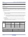
1
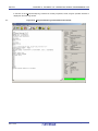
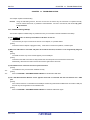
User’s Manual
PG-FP5
Flash Memory Programmer
User’s Manual
All information contained in these materials, including products and product specifications,
represents information on the product at the time of publication and is subject to change by
Renesas Electronics Corp. without notice. Please review the latest information published by
Renesas Electronics Corp. through various means, including the Renesas Electronics Corp.
website (http://www.renesas.com).
www.renesas.com
Rev. 5.00
Dec, 2011
Notice
1.
2.
3.
4.
5.
6.
7.
All information included in this document is current as of the date this document is issued. Such information, however, is
subject to change without any prior notice. Before purchasing or using any Renesas Electronics products listed herein, please
confirm the latest product information with a Renesas Electronics sales office. Also, please pay regular and careful attention to
additional and different information to be disclosed by Renesas Electronics such as that disclosed through our website.
Renesas Electronics does not assume any liability for infringement of patents, copyrights, or other intellectual property rights
of third parties by or arising from the use of Renesas Electronics products or technical information described in this document.
No license, express, implied or otherwise, is granted hereby under any patents, copyrights or other intellectual property rights
of Renesas Electronics or others.
You should not alter, modify, copy, or otherwise misappropriate any Renesas Electronics product, whether in whole or in part.
Descriptions of circuits, software and other related information in this document are provided only to illustrate the operation of
semiconductor products and application examples. You are fully responsible for the incorporation of these circuits, software,
and information in the design of your equipment. Renesas Electronics assumes no responsibility for any losses incurred by
you or third parties arising from the use of these circuits, software, or information.
When exporting the products or technology described in this document, you should comply with the applicable export control
laws and regulations and follow the procedures required by such laws and regulations. You should not use Renesas
Electronics products or the technology described in this document for any purpose relating to military applications or use by
the military, including but not limited to the development of weapons of mass destruction. Renesas Electronics products and
technology may not be used for or incorporated into any products or systems whose manufacture, use, or sale is prohibited
under any applicable domestic or foreign laws or regulations.
Renesas Electronics has used reasonable care in preparing the information included in this document, but Renesas Electronics
does not warrant that such information is error free. Renesas Electronics assumes no liability whatsoever for any damages
incurred by you resulting from errors in or omissions from the information included herein.
Renesas Electronics products are classified according to the following three quality grades: “Standard”, “High Quality”, and
“Specific”. The recommended applications for each Renesas Electronics product depends on the product’s quality grade, as
indicated below. You must check the quality grade of each Renesas Electronics product before using it in a particular
application. You may not use any Renesas Electronics product for any application categorized as “Specific” without the prior
written consent of Renesas Electronics. Further, you may not use any Renesas Electronics product for any application for
which it is not intended without the prior written consent of Renesas Electronics. Renesas Electronics shall not be in any way
liable for any damages or losses incurred by you or third parties arising from the use of any Renesas Electronics product for an
application categorized as “Specific” or for which the product is not intended where you have failed to obtain the prior written
consent of Renesas Electronics. The quality grade of each Renesas Electronics product is “Standard” unless otherwise
expressly specified in a Renesas Electronics data sheets or data books, etc.
“Standard”:
8.
9.
10.
11.
12.
Computers; office equipment; communications equipment; test and measurement equipment; audio and visual
equipment; home electronic appliances; machine tools; personal electronic equipment; and industrial robots.
“High Quality”: Transportation equipment (automobiles, trains, ships, etc.); traffic control systems; anti-disaster systems; anticrime systems; safety equipment; and medical equipment not specifically designed for life support.
“Specific”:
Aircraft; aerospace equipment; submersible repeaters; nuclear reactor control systems; medical equipment or
systems for life support (e.g. artificial life support devices or systems), surgical implantations, or healthcare
intervention (e.g. excision, etc.), and any other applications or purposes that pose a direct threat to human life.
You should use the Renesas Electronics products described in this document within the range specified by Renesas Electronics,
especially with respect to the maximum rating, operating supply voltage range, movement power voltage range, heat radiation
characteristics, installation and other product characteristics. Renesas Electronics shall have no liability for malfunctions or
damages arising out of the use of Renesas Electronics products beyond such specified ranges.
Although Renesas Electronics endeavors to improve the quality and reliability of its products, semiconductor products have
specific characteristics such as the occurrence of failure at a certain rate and malfunctions under certain use conditions. Further,
Renesas Electronics products are not subject to radiation resistance design. Please be sure to implement safety measures to
guard them against the possibility of physical injury, and injury or damage caused by fire in the event of the failure of a
Renesas Electronics product, such as safety design for hardware and software including but not limited to redundancy, fire
control and malfunction prevention, appropriate treatment for aging degradation or any other appropriate measures. Because
the evaluation of microcomputer software alone is very difficult, please evaluate the safety of the final products or system
manufactured by you.
Please contact a Renesas Electronics sales office for details as to environmental matters such as the environmental
compatibility of each Renesas Electronics product. Please use Renesas Electronics products in compliance with all applicable
laws and regulations that regulate the inclusion or use of controlled substances, including without limitation, the EU RoHS
Directive. Renesas Electronics assumes no liability for damages or losses occurring as a result of your noncompliance with
applicable laws and regulations.
This document may not be reproduced or duplicated, in any form, in whole or in part, without prior written consent of Renesas
Electronics.
Please contact a Renesas Electronics sales office if you have any questions regarding the information contained in this
document or Renesas Electronics products, or if you have any other inquiries.
(Note 1) “Renesas Electronics” as used in this document means Renesas Electronics Corporation and also includes its majorityowned subsidiaries.
(Note 2) “Renesas Electronics product(s)” means any product developed or manufactured by or for Renesas Electronics.
This equipment complies with the EMC protection requirements
WARNING
This is a ‘Class A’ (EN 55022: 1998) equipment. This equipment can cause radio
frequency noise when used in the residential area. In such cases, the user/operator
of the equipment may be required to take appropriate countermeasures under his
responsibility.
EEDT-ST-001-11
CAUTION
This equipment should be handled like a CMOS semiconductor device. The user
must take all precautions to avoid build-up of static electricity while working with this
equipment. All test and measurement tool including the workbench must be
grounded. The user/operator must be grounded using the wrist strap. The
connectors and/or device pins should not be touched with bare hands.
EEDT-ST-004-10
For customers in the European Union only
Redemption of Waste Electrical and Electronic Equipment
(WEEE) in accordance with legal regulations applicable in the
European Union only: This equipment (including all accessories)
is not intended for household use. After use the equipment cannot
be disposed of as household waste. Renesas Electronics Europe
GmbH offers to take back the equipment. All you need to do is
register at http://www.renesas.eu/weee.
EMC regulation (VCCI, FCC)
Please read the following notes about EMC regulation before using.
About FCC
Note: This equipment has been tested and found to comply with the limits for a Class
A digital device, pursuant to part 15 of the FCC Rules. These limits are designed to
provide reasonable protection against harmful interference when the equipment is
operated in a commercial environment. This equipment generates, uses and can
radiate radio frequency energy and, if not installed and used in accordance with the
instruction manual, may cause harmful interference to radio communications.
Operation of this equipment in a residential area is likely to cause harmful
interference in which case the user will be required to correct the interference at his
own expense.
Modifications not expressly approved by the manufacturer could void the user's
authority to operated the equipment under FCC rules.
CAUTION:
When using this product, please use AC adapter (QB-COMMON-PW) which comply with the
standard of VCCI and FCC.
General Precautions on Handling This Product
1. Circumstances not covered by product guarantee
If the product was disassembled, altered, or repaired by the customer
If it was dropped, broken, or given another strong shock
Use at overvoltage, use outside guaranteed temperature range, storing outside guaranteed temperature range
If power was turned on while the AC adapter, interface cable, or connection to the target system was in an
unsatisfactory state
If the cable of the AC adapter, the interface cable, the target cable, or the like was bent or pulled excessively
If the product got wet
If the product and target system were connected while a potential difference existed between the GND of the
product and the GND of the target system
If a connector or cable was connected or disconnected while power was being supplied to the product
If an excessive load was applied to a connector or cable
If the product is used or stored in an environment where an electrostatic or electrical noise is likely to occur
2. Safety precautions
If used for a long time, the product may become hot (50 to 60C). Be careful of low temperature burns and
other dangers due to the product becoming hot.
Be careful of electrical shock. There is a danger of electrical shock if the product is used as described above in
1 Circumstances not covered by product guarantee.
How to Use This Manual
.
Target Readers
This manual is intended for users who use the PG-FP5 when designing and
developing a system using a Renesas Electronics on-chip flash memory
microcontroller.
Purpose
This manual is intended to give users an understanding of the basic specifications
and correct use of the PG-FP5. By using the PG-FP5, programs can be easily erased
from or written to the flash memory of a Renesas Electronics on-chip flash memory
microcontroller, or can be verified on WindowsTM screens, while the microcontroller is
mounted on the user board.
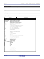
Organization
This manual includes the following sections.
Overview
Hardware installation
Software installation
Programming GUI usage
Example of operation using programming GUI
PG-FP5 operation in standalone mode
Usage the remote connector
Usage communication commands
Connectors and cables
Notes on target system designs
Target interface specifications
Troubleshooting
Messages
Supplementary information
Electrical specifications of target interface
Electrical specifications of remote interface
How to Read This Manual
It is assumed that the readers of this manual have general knowledge of electricity,
logic circuits, and microcontrollers.
To understand the overall operation
Read this manual according to the CONTENTS.
The mark <R> shows major revised points. The revised points can be easily
searched by copying an “<R>” in the PDF file and specifying it in the “Find what:”
field.
To know the cautions of target system
See the CHAPTER 9 CONNECTORS AND CABLES, CHAPTER 10 NOTES ON
TARGET SYSTEM DESIGNS, and CHAPTER 11 SPECIFICATION OF TARGET
INTERFACE CIRCUITS. Also see the user’s manual for each target device.
Conventions
Note: Footnote for item marked with Note in the text.
Caution: Information requiring particular attention
Remark: Supplementary information
Binary ... or B
Numeral representation:
Decimal ...
Hexadecimal ... 0x or h
“ ”: Any character or item on screen
[ ]: Name of commands, dialog boxes or area
<R>
Terminology
The meanings of the terms used in this manual are as follows.
Term
Meaning
FP5
Abbreviation of the flash memory programmer PG-FP5
Programming GUI
Windows application to operate FP5 using programming GUI
Target device
Renesas Electronics on-chip flash memory microcontroller
Target system
User-designed board on which target device is mounted
Note1
Program adapter
Conversion adapter to write programs to target device
PR5 file
Abbreviation of the parameter file for the PG-FP5.
The parameter file has parameter information required to write in the flash
memory of the target microcontroller. The extension of the file is "*.pr5". Do
not change the data in the file. If the file is changed, operation of the FP5 is not
guaranteed.
ESF file
Abbreviation of the setting file for the PG-FP5.
The setting file stores information required for writing. For the FP5, settings
regarding the writing environment such as target devices and operation option
are stored. The extension of the file is "*.esf". Do not change the data in the
file. If the file is changed, operation of the FP5 is not guaranteed.
Program file
The program file is the program written to the microcontroller. For the FP5, the
following file formats are supported.
<RL78, 78K, V850>
a. Intel HEX format HEX file
b. Intel HEX format HCUHEX file
c. Motorola S format HEX file
d. Motorola S format HCUHEX file
<RX family, R8C family, SuperH family>
a. Intel HEX format HEX file
b. Motorola S format HEX file
c. DDI file
Notes 1. Addresses may not be consecutive, but they must be in ascending
order.
Free space will be filled with "FFH" upon download to the
FP5. When download is performed with the programming GUI, it has
the function to sort addresses in ascending order.
2. For details on the formats, refer to "How to Order ROM Code:
Information (C10302E)."
3. The program file name does not support 2-byte characters.
Flash options
General term for security settings, rewrite protection settings, reset vector
handling function settings, option byte settings, and on-chip debug security ID
settings
Note2
Option data
General term for flash options, wide-voltage mode, and full-speed mode
HEX file
A HEX file of Intel HEX format type or Motorola HEX format type without option
data
HCUHEX file
A HEX file that integrates option data into a HEX file generated by using the
HEX Consolidation Utility (HCU), which is used to generate ROM code for flash
memory products whose flash memories are pre-written by Renesas Electronics
DDI file
File in which data in multiple flash areas generated by Flash Development
Toolkit is integrated.
Flash
Development
Toolkit
Flash Development Toolkit is a software to write in the flash memory of the
Renesas microcontroller with on-chip flash. For details, refer to the following
websites.
INI file
Japanese version:
http://japan.renesas.com/fdt
English version:
http://www.renesas.com/fdt
File in which settings of the programming GUI are stored. The file is saved
when the programming GUI is closed. The file name is "FP5.ini".
Storage location in Windows XP
C:\Windows
Storage location in Windows Vista,Windows 7
C:\Users\(user name)\AppData \Local\VirtualStore\Windows
OCD security ID
Abbreviation of the on-chip debug security ID.
Security function for on-chip
debugging of the microcontroller.
ID code
Function to prohibit read, write, or erasure from the host. The control code on
the ROM and ID code are used to enable or disable ID code protect and to
determine ID code protect.
Lock bit
Function to prevent data write/erasure by mistake. Write and erasure can be
prohibited (locked) for each block.
Signature
Information about the microcontroller (microcontroller name, firmware version)
Notes 1. The program adapter (FA-xxxx) is a product of Naito Densei Machida Mfg. Co., Ltd.
If you have any questions about the FA adapter board, contact Naito Densei Machida
Mfg. Co., Ltd. (Tel: +81-42-750-4172).
2. The functions that can be used differ depending on the target device.
All trademarks and registered trademarks are the property of the respective owner.
CONTENTS
CHAPTER 1 OVERVIEW ......................................................................................................................... 13
1.1 Features..................................................................................................................................... 13
1.2 Writing Quality .......................................................................................................................... 13
1.3 Supported Devices ................................................................................................................... 13
1.4 FP5 System Overview .............................................................................................................. 14
1.5 Operating Environment............................................................................................................ 16
1.5.1 Hardware environment....................................................................................................................16
1.5.2 Software environment .....................................................................................................................16
1.6
1.7
1.8
Hardware Specifications.......................................................................................................... 17
AC Adapters for PG-FP5 .......................................................................................................... 18
HCUHEX Files ........................................................................................................................... 19
CHAPTER 2 HARDWARE CONFIGURATION ...................................................................................... 20
2.1 Package Contents .................................................................................................................... 20
2.2 System Configuration .............................................................................................................. 20
2.2.1 Host machine ..................................................................................................................................21
2.2.2 Serial cable .....................................................................................................................................21
2.2.3 USB cable.......................................................................................................................................21
2.2.4 AC adapter......................................................................................................................................21
2.2.5 Target cable....................................................................................................................................21
2.2.6 GND cable ......................................................................................................................................21
2.2.7 Target system .................................................................................................................................21
2.2.8 Program adapter .............................................................................................................................21
2.3
Names and Functions on Main Unit ....................................................................................... 22
2.3.1 FP5 control panel............................................................................................................................22
2.3.2 FP5 connectors...............................................................................................................................23
CHAPTER 3 SOFTWARE INSTALLATION ........................................................................................... 26
3.1 Obtaining Software................................................................................................................... 26
3.2 Installation................................................................................................................................. 26
3.2.1 Notes on installation........................................................................................................................27
3.3
3.4
Uninstallation ............................................................................................................................ 28
Updating Programming GUI, Firmware and FPGA ............................................................... 28
3.4.1 Checking the current version ..........................................................................................................29
3.4.2 Installation of programming GUI .....................................................................................................29
3.4.3 Installation of firmware update ........................................................................................................30
3.4.4 Installation of FPGA update ............................................................................................................33
CHAPTER 4 PROGRAMMING GUI USAGE ......................................................................................... 38
4.1 Introduction............................................................................................................................... 38
4.2 Startup of Programming GUI................................................................................................... 38
4.3 Menu Bar ................................................................................................................................... 42
4.3.1 [File] menu ......................................................................................................................................42
4.3.2 [Programmer] menu ........................................................................................................................52
4.3.3 [Device] menu .................................................................................................................................69
4.3.4 [Help] menu ..................................................................................................................................109
4.4
4.5
4.6
Toolbar..................................................................................................................................... 110
Action Log Window ................................................................................................................ 111
Programming Parameter Window......................................................................................... 112
4.7
4.8
Status Bar................................................................................................................................ 113
Hint Bar.................................................................................................................................... 114
CHAPTER 5 EXAMPLE OF OPERATION USING PROGRAMMING GUI ...................................... 115
CHAPTER 6 USAGE IN STANDALONE MODE ................................................................................ 130
6.1 Before Starting Standalone Operation ................................................................................. 130
6.2 Description of Buttons, Message Display and Status LEDs.............................................. 130
6.3 Standalone Operation Menu.................................................................................................. 132
6.3.1 [Commands] menu........................................................................................................................132
6.3.2 [Type Setting] menu......................................................................................................................134
6.3.3 [Option Setting] menu ...................................................................................................................135
6.3.4 [Voltage Setting] menu..................................................................................................................137
6.3.5 [Utility/Misc.] menu........................................................................................................................138
CHAPTER 7 USAGE THE REMOTE CONNECTOR.......................................................................... 139
7.1 Remote Interface Mode .......................................................................................................... 139
7.2 Remote Connector Pins......................................................................................................... 139
7.3 Equivalence Circuits .............................................................................................................. 141
7.4 External Connection Example............................................................................................... 142
CHAPTER 8 USAGE COMMUNICATION COMMANDS .................................................................... 143
8.1 Starting the Communications Software............................................................................... 143
8.2 Command List......................................................................................................................... 146
8.3 Description of Commands..................................................................................................... 148
8.4 Description of FP5 Control Commands ............................................................................... 149
8.4.1 autocon command ........................................................................................................................149
8.4.2 brt command.................................................................................................................................150
8.4.3 conf command ..............................................................................................................................151
8.4.4 downprm command ......................................................................................................................154
8.4.5 downset command........................................................................................................................155
8.4.6 fcks command...............................................................................................................................156
8.4.7 files command...............................................................................................................................157
8.4.8 fpga_up command ........................................................................................................................158
8.4.9 hex command ...............................................................................................................................159
8.4.10 hlp command ................................................................................................................................160
8.4.11 lod command ................................................................................................................................161
8.4.12 prm command ...............................................................................................................................162
8.4.13 progarea command.......................................................................................................................163
8.4.14 pwr_off command .........................................................................................................................164
8.4.15 res command ................................................................................................................................165
8.4.16 security command.........................................................................................................................165
8.4.17 selftest command..........................................................................................................................166
8.4.18 sound command ...........................................................................................................................167
8.4.19 srec command ..............................................................................................................................168
8.4.20 trc command .................................................................................................................................169
8.4.21 upprm command ...........................................................................................................................170
8.4.22 upset command ............................................................................................................................171
8.4.23 ver command ................................................................................................................................171
8.4.24 version_up command....................................................................................................................172
8.5
Description of The FP5 Device Commands ......................................................................... 174
8.5.1 bln command ................................................................................................................................174
8.5.2 con command ...............................................................................................................................175
8.5.3 dcon command .............................................................................................................................175
8.5.4 ep/epv command ..........................................................................................................................176
8.5.5 ers command ................................................................................................................................177
8.5.6 gid command ................................................................................................................................178
8.5.7 gob command ...............................................................................................................................179
8.5.8 gos command ...............................................................................................................................180
8.5.9 gsc command ...............................................................................................................................181
8.5.10 idc command ................................................................................................................................182
8.5.11 opb command ...............................................................................................................................183
8.5.12 prg command ................................................................................................................................184
8.5.13 read command ..............................................................................................................................185
8.5.14 scf command ................................................................................................................................186
8.5.15 sig command ................................................................................................................................187
8.5.16 slb command ................................................................................................................................188
8.5.17 sum command ..............................................................................................................................189
8.5.18 vrf command .................................................................................................................................190
CHAPTER 9 CONNECTORS AND CABLES ...................................................................................... 191
9.1 Power Supply Connector....................................................................................................... 191
9.2 Serial Connector..................................................................................................................... 192
9.2.1 Serial cable ...................................................................................................................................193
9.3
USB Connector ....................................................................................................................... 193
9.3.1 USB cable.....................................................................................................................................193
9.4
Target Connector.................................................................................................................... 194
9.4.1 Target Cable (16-pin type) ............................................................................................................195
9.4.2 Target cable (14-pin type) .............................................................................................................196
9.5
GND Connector....................................................................................................................... 198
9.5.1 GND cable ....................................................................................................................................198
9.6
Remote Connector ................................................................................................................. 198
CHAPTER 10 NOTES ON TARGET SYSTEM DESIGN ................................................................... 199
CHAPTER 11 SPECIFICATIONS OF TARGET INTERFACE CIRCUITS ........................................ 209
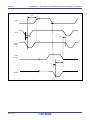
¯¯¯¯¯¯and SCK........................................................................................................ 209
11.1 SO/TxD, RESET
11.2 SI/RxD and H/S........................................................................................................................ 209
11.3 CLK .......................................................................................................................................... 210
11.4 FLMD0 and FLMD1 ................................................................................................................. 210
11.5 VDD and VDD2 ............................................................................................................................ 211
11.6 VPP ............................................................................................................................................ 211
CHAPTER 12 TROUBLESHOOTING.................................................................................................... 212
12.1 Problems During Startup ....................................................................................................... 212
12.2 Problems During Operation................................................................................................... 213
APPENDIX A MESSAGES...................................................................................................................... 216
A.1 Message Format ..................................................................................................................... 216
A.2 Error/Warning Dialog Boxes for Programming GUI Operation ......................................... 217
A.3 Information Dialog Boxes for Programming GUI Operation .............................................. 220
A.4 Error Messages Displayed in FP5 Message Display........................................................... 223
APPENDIX B SUPPLEMENTARY INFORMATION ............................................................................. 226
APPENDIX C ELECTRICAL SPECIFICATIONS OF TARGET INTERFACE ................................... 229
C.1 Absolute Maximum Ratings (TA = 0 to 40 C) ...................................................................... 229
C.2 DC Characteristics (TA = 0 to 40 C) ..................................................................................... 230
C.3 AC Characteristics (TA = 0 to 40 C, C = 0 pF (Unloaded Condition)) ............................... 231
C.3.1 CLK output characteristics (TA = 0 to 40 C, C = 0 pF (unloaded condition))................................233
C.3.2 Serial transfer timing (TA = 0 to 40 C, C = 0 pF (unloaded condition)).........................................234
APPENDIX D ELECTRICAL SPECIFICATIONS OF REMOTE INTERFACE .................................. 235
D.1 Absolute Maximum Ratings (TA = 0 to 40 °C) ...................................................................... 235
D.2 DC Characteristics TA = 0 to 40 C, C = 0 pF (Unloaded Condition)) ................................ 236
D.3 AC Characteristics (TA = 0 to 40 °C, C = 0 pF (Unloaded Condition)) ............................... 237
D.3.1 Standard mode .............................................................................................................................237
D.3.2 Bank mode....................................................................................................................................239
D.3.3 Simple mode .................................................................................................................................241
PG-FP5
CHAPTER 1 OVERVIEW
CHAPTER 1 OVERVIEW
The FP5 is a tool that erases, writes and verifies programs on a Renesas Electronics on-chip flash memory
microcontroller on the target system or program adapter.
1.1
Features
Compatible with remote operation for FP5 from an external control device
Compatible with communications commands operated by the FP5 command through RS-232C
The customization and security settings of the FP5 unit can be changed with the FP5 Manager function
Supports on-chip 2-power-supply flash memory microcontrollers and single-power-supply on-chip flash memory
microcontrollers
Supports flash memory programming through the programming GUI using the host machine (programming GUI
operation) and operation in standalone (standalone operation)
Supports on-board programming through which programs are written with the target device mounted on the target
system, and off-board programming through which programs are written via a program adapter without the target
device mounted on the target system
Program files can be saved in the 16 MB flash memory in the FP5 (divided by 4, in 4 MB units or divided by 8, in 2
MB units)
Device-specific parameters required for programming can be saved in the FP5 internal flash memory by using the
parameter file (PR5 file), together with programming settings (ESF file).
Multiple program files, PR5 files and ESF files can be saved
Supports CSI, CSI + HS, UART, I2C and PORT as target device interfaces
Can supply VDD and clocks to the target device
Supports USB interface and serial interface (RS-232C) as a host interface
Supports self-testing function
Can update firmware and FPGA
Compact and lightweight
1.2
Writing Quality
Thoroughly confirm, verify and evaluate the following points before using the FP5, in order to improve the writing quality.
Design circuits as described in the user’s manual for the target device and the FP5.
Use the device and the FP5 as described in the user’s manual for each product.
The power supplied to the target device is stable.
<R> 1.3
Supported Devices
The FP5 supports on-chip 2-power-supply flash memory microcontrollers and on-chip single-power-supply flash
memory microcontrollers.
FP5 parameter files (PR5 files) corresponding to the supported devices are posted on the following website.
URLs
Japanese version: http://japan.renesas.com/pg_fp5
English version (Except for Europe area): http://www.renesas.com/pg_fp5
English version (For Europe area): http://www.renesas.eu/update Section PG-FP5-EE
R20UT0008EJ0500 Rev. 5.00
2011.12.26
Page 13 of 254
PG-FP5
1.4
CHAPTER 1 OVERVIEW
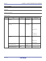
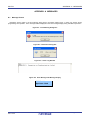
FP5 System Overview
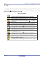
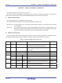
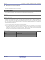
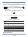
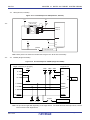
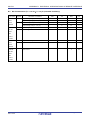
The FP5 system overview is shown in the following diagrams.
Figure 1-1. FP5 Connection Image
Communications
command operation
Serial cable
PR5 file
or
ESF file
USB cable
AC adapter
Programming
environment setting
HEX editor changes
the memory contents
Checksum calculation
Self-testing function
Saved in FP5 internal
flash memory
16MB
Buzzer function
Saving log files
Standalone operation
Downloading
program files
External control
devices
Target cable
GND cable
INI file
Programming GUI operation
Built-in 16 MB flash memory for
saving program files
Files are divided by 4, in 4 MB
units or divided by 8, in 2 MB
units
Target system or program adapter
Remote Operation
R20UT0008EJ0500 Rev. 5.00
2011.12.26
Manager function
(passwords, security,
customization, etc.)
setting
Page 14 of 254
PG-FP5
CHAPTER 1 OVERVIEW
<Programming GUI operation>
<R>
The following operations can be performed with the programming GUI. For USB connection, the USB driver must be
installed. The settings on the host machine are saved in an INI file.
ESF file creation
Downloading program files, PR5 files and ESF files (saved into FP5 internal flash memory)
Saving log files
Editing program files (by using HEX editor)
Checksum calculation
Programming command execution
Execution of self-testing function
Manager function (passwords, security, customization, etc.) setting
<Standalone operation>
The FP5 can operate in standalone mode, whereby commands such as [Erase], [Program] and [Autoprocedure(E.P.)]
can be executed without using the host machine. It is suitable for use in production lines during mass production or
upgrading programs in the field.
The following can be performed in standalone operation.
Execute programming command
Confirm contents of each downloaded file
<Communications Command Operation>
FP5 can be operated by communications commands from the host machine.
<Remote Operation>
Writing and PASS/ERROR displays can be operated and confirmed from external control devices.
<FP5 internal flash memory>
The FP5 has a 16 MB flash memory area for saving program files. This memory area can be used as four 4 MB
programming areas (Area 0 to Area 3) or eight independent 2 MB programming areas (Area 0 to Area 7). Program files
can be downloaded to each programming area, and which file, PR5 or ESF, is to be saved is selectable in programming
area units. That is, files can be individually downloaded in each programming area, and the area used can also be
selected individually. Program files, PR5 files and ESF files are retained even if the FP5 power is turned off.
Downloaded data will be self-tested for accuracy when the FP5 is started, during downloads and when programming
areas are changed.
<Notification function>
When Autoprocedure (E.P.) is executed, whether execution is completed normally is indicated by beeps.
<Checksum calculation>
Checksum calculation for the download program files is possible.
R20UT0008EJ0500 Rev. 5.00
2011.12.26
Page 15 of 254
PG-FP5
1.5
CHAPTER 1 OVERVIEW
Operating Environment
This section explains the following items with respect to the operating environment.
Hardware environment
Software environment
1.5.1
Hardware environment
(1) Host machines
PC/ATTM compatible
<R>
Equipped with USB 2.0 ports (compatible with 1.1)
Equipped with RS-232C serial ports
(2) Hardware option tools that support FP5
Target board QB-xxxx-TB (a product of Renesas Electronics, sold separately)
Program adapter FA-xxxx (a product of Naito Densei Machida Mfg. Co., Ltd., sold separately)
IC clip type target cable FA-CLIP (a product of Naito Densei Machida Mfg. Co., Ltd., sold separately)
Switch jig FL-SW/FP5 (a product of Naito Densei Machida Mfg. Co., Ltd., sold separately)
Buffer board FL-BUF (a product of Naito Densei Machida Mfg. Co., Ltd., sold separately)
Long target cable FL-TCxxxx (name undetermined, a product of Naito Densei Machida Mfg. Co., Ltd., sold
separately)
Conversion adapter FL-RL78/FP5 (a product of Naito Densei Machida Mfg. Co., Ltd., sold separately) used when
<R>
VDD EVDD for the RL78 family
1.5.2
<R>
Software environment
(1) OS (either of the following)
Windows XP (32-bit edition)
Windows VistaTM (32-bit edition, 64-bit edition)
Windows 7 (32-bit edition, 64-bit edition)
Microsoft .NET Framework 3.5 SP1 + Language pack
Microsoft Visual C++ 2008 SP1 Redistributable Package (x86)
Internet Explorer® 6.0 or later
(2) Software option tools that support FP5
Simplified control software for production line (FPterm) (a product of Naito Densei Machida Mfg. Co., Ltd., sold
Note
separately)
Gang-supported software for production line (FW-GFP) (a product of Naito Densei Machida Mfg. Co., Ltd., sold
separately)
Note Under development
R20UT0008EJ0500 Rev. 5.00
2011.12.26
Page 16 of 254
PG-FP5
1.6
CHAPTER 1 OVERVIEW
Hardware Specifications
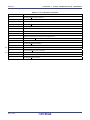
Table 1-1. Hardware Specifications
Hardware
Items
Specifications
FP5 main
Operating power supply
Supplied via AC adapter (15 V)
unit
Operating environment
Temperature: 0 to +40C
ccondition
Humidity: 10% to 80% RH (no condensation)
Storage environment
Temperature: 15 to +60C
ccondition
Humidity: 10% to 80% RH (no condensation)
Package size
140 90 30 mm (not including projections)
Weight
Approximately 230 g
Internal flash memory
Program file save area (16 MB)
Other (PR5 file save area, ESF file saved area, firmware area, and FPGA area)
Operation mode
Programming GUI operation, standalone operation, remote operation, communication
command operation
AC adapter
<R> Host
machine
Note 3
Specifications
AC adapters used in each region
Target host machine
PC/AT compatible
USB connector
Type mini-B, USB 2.0 (compatible with 1.1)
USB cable
Approximately 2 m
Serial connector
9-pin D-SUB male connector for RS-232C @ 9600, 19200, 38400, 57600, 115200 bps
Serial cable
Approximately 3 m (cross cable)
Target connector
Connector:
interface
Target
interface
Note 1
15-pin HD-SUB female connector
Protected function: Internal over-voltage input protection circuit
Supported communication mode and rate:
3-wire serial I/O (CSI) (5.0 MHz max.)
3-wire serial I/O with handshake (CSI + HS) (5.0 MHz max.)
Pseudo 3-wire I/O (2.0 kHz max.)
UART (1 Mbps max.)
2
I C (100 kHz max.)
Target cable
<R>
Two cables: 16-pin type and 14-pin type. Cable length: Approximately 42 cm
Note 2
Remote
Power supply
1.2 to 5.5 V
Power supply detection
Available. Current consumption: 1 mA or less
CPU clock supply
1 MHz, 2 MHz, 4 MHz, 5 MHz, 6 MHz, 8 MHz, 9 MHz, 10 MHz, 12 MHz, 16 MHz, 20 MHz
GND cable
Approximately 1 m
Remote connector
15-pin D-SUB female connector
interface
Notes 1. The maximum communication speed in the interface may vary depending on the device and environment
used.
2. VDD for the target system is supplied for the purpose of supplying power to the target device through which
writing is performed, so the specification cannot secure sufficient capacity to operate the target system. Use
the power source on the target system when performing on-board programming.
3. The AC adapter differs depending on the region where the product is being used. For details, see Table 1-2
AC Adapters for PG-FP5 Used in Each Region. An AC adapter is required when using the PG-FP5, so be
sure to purchase an AC adapter.
R20UT0008EJ0500 Rev. 5.00
2011.12.26
Page 17 of 254
PG-FP5
1.7
CHAPTER 1 OVERVIEW
AC Adapters for PG-FP5
The specifications of the AC adapter for the PG-FP5 differ depending on the region where the product is being used.
Be sure to use the appropriate AC adapter for your region. Note that an AC adapter is not included with the PG-FP5. The
appropriate AC adapter must be purchased separately.
Table 1-2. AC Adapters for PG-FP5 Used in Each Region
Name
Region
Notes 1, 2
Note 3
Part Number
AC adapter
Japan
QB-COMMON-PW-JP
(sold separately)
USA
QB-COMMON-PW-EA
China
QB-COMMON-PW-CN
Hong Kong
QB-COMMON-PW-HK
Korea
QB-COMMON-PW-KR
Singapore
QB-COMMON-PW-SG
Chinese Taipei
QB-COMMON-PW-TW
Notes 1. The AC adapter corresponding to the region from which the order was received will be shipped.
2. For regions other than those listed above, please contact a Renesas Electronics sales representative or
distributor.
3. You can only order the AC adapter that can be used in your region.
R20UT0008EJ0500 Rev. 5.00
2011.12.26
Page 18 of 254
PG-FP5
<R> 1.8
CHAPTER 1 OVERVIEW
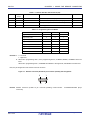
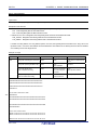
HCUHEX Files
HCUHEX files are files that are required when ordering flash memory products whose flash memories are pre-written
by Renesas Electronics. HCUHEX files are generated by the HEX Consolidation Utility (HCU), after which they must be
verified on a flash memory programmer before being submitted. The PG-FP5 handles HCUHEX files as master data,
and can therefore be used to check the written data and the option data settings. HCUHEX files are supported in part of
the RL78, 78K0, 78K0R, V850. If they are supported, it is described in the user's manual of the target microcontroller
(the SH, RX, and R8C do not support HCUHEX files). For details, see the functional descriptions in this manual. For
more information about HCU, see the HCU user's manual or the manual of the target device. The following websites
describe details about HCU.
Websites
Japanese version: http://japan.renesas.com/hcu
English version:
https://www5.renesas.com/micro/tool_reg/OdsListTool.do?code=640&lang=en
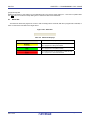
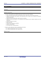
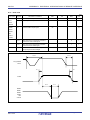
Figure 1-2. PG-FP5 Connection Diagram
HEX file
PR5 file
ESF file
Target system
HCUHEX
file
HCU
R20UT0008EJ0500 Rev. 5.00
2011.12.26
Operation
verified on
PG-FP5
HCUHEX file submitted
for ordering pre-written
flash memory products
Page 19 of 254
PG-FP5
CHAPTER 2 HARDWARE CONFIGURATION
CHAPTER 2 HARDWARE CONFIGURATION
This chapter explains the following items for hardware configuration.
Package contents
System configuration
Names and functions on main unit
2.1
Package Contents
Please verify that you have received all the parts listed in the package contents list included with the FP5 package. If
any part is missing or seems to be damaged, please contact a Renesas Electronics sales representative or distributor.
2.2
System Configuration
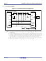
The FP5 system configuration is as shown in the diagram below.
Figure 2-1. FP5 System Configuration
Serial cable
or
USB cable
AC adapter
Host machine
FP5
External control
devices
Target cable
GND cable
Target system or Program adapter
Notes 1. The target system and program adapter are not included in the FP5 package.
2. The program adapter is a product of Naito Densei Machida Mfg. Co., Ltd.
The FP5 is connected to the host machine via a serial cable or a USB cable. The FP5 is connected to the target
system via a target cable and a GND cable. And the FP5 can be remote controlled by connecting the remote connector
and external control device.
R20UT0008EJ0500 Rev. 5.00
2011.12.26
Page 20 of 254
PG-FP5
2.2.1
<R>
CHAPTER 2 HARDWARE CONFIGURATION
Host machine
A host machine is used to communicate with the FP5. The host machine must also be equipped with a serial port or a
USB port.
2.2.2
Serial cable
Communication is established by using a serial cable to connect the host machine serial port and FP5 serial connector
(RS-232C cross cable) connection. For details on the serial cable specifications, refer to CHAPTER 9 CONNECTORS
AND CABLES
2.2.3
USB cable
Communication is established by connecting the host machine USB port and the FP5 USB connector (mini-B type)
using a USB cable. For details on the USB cable specifications, refer to CHAPTER 9 CONNECTORS AND CABLES.
2.2.4
AC adapter
Connect the FP5 power supply connector to the AC adapter included with the FP5. The AC adapter differs depending
on the region where the product is being used. For details, see Table 1-2 AC Adapters for PG-FP5 Used in Each
Region. An AC adapter is required when using the PG-FP5, so be sure to purchase an AC adapter.
2.2.5
<R>
Target cable
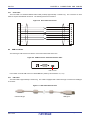
A 16-pin connector or 14-pin connector is equipped on the tip of the target cable, which is connected to the target
system or the program adapter. For details on the target cable specifications, refer to CHAPTER 9 CONNECTORS AND
CABLES.
2.2.6
GND cable
To reinforce the GND, use a GND cable to connect the FP5 GND connector and the signal GND of the target system or
program adapter. For details on the GND cable specifications, refer to CHAPTER 9 CONNECTORS AND CABLES.
Caution
The FP5 and target system may be damaged if the voltage between the FP5 GND and the target
system GND is different. Use the GND cable to match the voltage before connecting the target cable.
2.2.7
Target system
The target system must be equipped with a device interface that complies with the target cable specifications. For
details on the specifications, refer to CHAPTER 9 CONNECTORS AND CABLES, CHAPTER 10 NOTES ON TARGET
SYSTEM DESIGN, and CHAPTER 11 SPECIFICATIONS OF TARGET INTERFACE CIRCUITS.
2.2.8
Program adapter
The FP5 supports off-board programming through which programs are written via a program adapter (FA series)
without mounting the target device onto the target system. Program adapters corresponding to each type of the target
device package are available.
R20UT0008EJ0500 Rev. 5.00
2011.12.26
Page 21 of 254
PG-FP5
2.3
CHAPTER 2 HARDWARE CONFIGURATION
Names and Functions on Main Unit
This section describes the names and functions on the FP5 main unit.
2.3.1
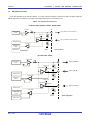
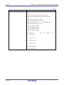
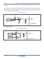
FP5 control panel
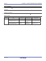
Indicators and buttons are laid out on the FP5 top.
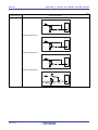
Figure 2-2. FP5 Top View <Control Panel>
POWER LED
POWER button
Message display
Status LEDs
Control buttons
(1) Indicators
POWER LED
LED that displays the FP5 power status.
A red LED is turned on when the FP5 is ON, and is turned off when the FP5 is OFF.
Message display An LCD display of 16 2-characters that indicates the operating mode or menus.
It is mainly used when the FP5 operates in standalone mode.
Status LEDs
LEDs that show the FP5 operating status.
PASS (green LED turned on) indicates normal completion, BUSY (orange LED flashes)
indicates processing in progress, and ERROR (red LED turned on) indicates abnormal
completion.
R20UT0008EJ0500 Rev. 5.00
2011.12.26
Page 22 of 254
PG-FP5
CHAPTER 2 HARDWARE CONFIGURATION
(2) Buttons
POWER button Used to turn on/off the power to the FP5. Press this button longer (for about 1 minute) when
NEXT button
turning on/off.
Proceeds to the next menu item at the same level in sequence.
ENTER button
Selects the item shown in the message display.
CANCEL button Cancels the current selection and returns to the previous menu item. The command currently
running cannot be stopped, except for the [Read] command.
START button
Remark
Executes the [Autoprocedure(E.P.)] command with a valid programming area setting.
The NEXT , ENTER , CANCEL and START buttons are mainly used in standalone mode.
When the FP5 Manager is used to switch to the bank mode or simple mode, the button functions and
message display functions will change. Refer to 4.3.2 (9) [FP5 Manager] Command and CHAPTER 7
USAGE THE REMOTE CONNECTOR.
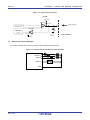
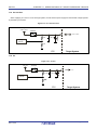
2.3.2
FP5 connectors
The power supply connector, serial connector and USB connector are laid out on the host interface side.
The target connector, GND connector and remote connector are laid out on the target connector side.
When the FP5 Manager is used to switch to the bank mode or simple mode, the button functions and message display
functions will change. Refer to 4.3.2 (9)
[FP5 Manager] Command and CHAPTER 7
USAGE THE REMOTE
CONNECTOR.
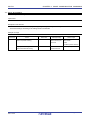
Figure 2-3. FP5 Top View <Connector>
USB connector
Target connector
R20UT0008EJ0500 Rev. 5.00
2011.12.26
Serial connector
GND connector
Power supply connector
Remote connector
Page 23 of 254
PG-FP5
CHAPTER 2 HARDWARE CONFIGURATION
Figure 2-4. FP5 Host Interface Side
Power supply connector
Serial connector
USB connector
Figure 2-5. FP5 Target Connector Side
Target connector
GND
connector
Remote
connector
(1) Power supply connector
Connect the power supply connector to the AC adapter included with the FP5. For details on the power supply
connector specifications, refer to CHAPTER 9 CONNECTORS AND CABLES.
<R>
Caution
Do not use an AC adapter other than that included with the PG-FP5.
(2) Serial connector
Communication is established by using a serial cable (RS-232C cross cable) connection to connect the host
machine serial port and FP5 serial connector. The data transfer conditions are as follows.
Data transfer speed: 9,600 bps, 19,200 bps, 38,400 bps, 57,600 bps, or 115,200 bps
Data bit: 8 bits
Parity: none
Stop bit: 1 bit
Flow control: hardware
The transfer speed is set to 9,600 bps by default, but it can be changed. For details on the serial connector
specifications, refer to CHAPTER 9 CONNECTORS AND CABLES.
(3) USB connector
Communication is established by using a USB cable to connect the host machine USB port and the FP5 USB
connector (mini-B type). This connector conforms with USB 2.0 standards. For details on the USB connector
specifications, refer to CHAPTER 9 CONNECTORS AND CABLES.
(4) Target connector
Connect the target connector to the target system using the target cable for on-board programming. Connect the
target connector to the program adapter using the target cable for off-board programming. For details on the target
connector specifications, refer to CHAPTER 9 CONNECTORS AND CABLES.
R20UT0008EJ0500 Rev. 5.00
2011.12.26
Page 24 of 254
PG-FP5
CHAPTER 2 HARDWARE CONFIGURATION
(5) GND connector
To reinforce the GND, connect the FP5 GND connector and the signal GND of the target system or program
adapter using a GND cable.
For details on the GND connector specifications, refer to CHAPTER 9
CONNECTORS AND CABLES.
Caution The FP5 and target system may be damaged if the voltage between the FP5 GND and the target
system GND is different. Use the GND cable to match the voltage before connecting the target
cable.
(6) Remote connector
The FP5 can be remote controlled by connecting the remote connector and external control device. For details on
the Remote operation, refer to CHAPTER 7 USAGE THE REMOTE CONNECTOR, CHAPTER 9 CONNECTORS
AND CABLES.
R20UT0008EJ0500 Rev. 5.00
2011.12.26
Page 25 of 254
PG-FP5
CHAPTER 3 SOFTWARE INSTALLATION
CHAPTER 3 SOFTWARE INSTALLATION
This chapter explains the following items related to installation.
Obtaining software
Installation
Uninstallation
Updating programming GUI, firmware and FPGA
<R> 3.1
Obtaining Software
Download the programming GUI, USB driver, and FP5 parameter file (PR5 file) from the following Renesas Electronics
website.
URLs Japanese version: http://japan.renesas.com/pg_fp5
English version (Except for Europe area): http://www.renesas.com/pg_fp5
English version (For Europe area):
Caution
3.2
http://www.renesas.eu/update Section PG-FP5-EE
Use of the latest version of software is recommended to assure the FP5 operation.
Installation
This section explains the installation procedure for the programming GUI, USB driver and parameter file (PR5 file).
Table 3-1. Installation
<R>
Installation Order
1
Item
Method
Programming
Run the downloaded executable file (PG-FP5_Package_Vxxx.exe) and perform installation,
GUI, USB driver
following the directions on the installer screen. After installation, the USB driver detects the
FP5 by plug-and-play, and it is automatically added.
2
Decompress the downloaded file to any folder. A *.pr5 file is decompressed into any folder, so
PR5 file
copy it to the FP5_PRJ folder where the programming GUI is installed.
The folder configuration after programming GUI installation is as follows.
<R> C:\
\Program Files
Folder specified as the installation destination (C:\Program Files\Common Files (x86)\Renesas
Electronics for the 64-bit version of Windows)
\Renesas Electronics
\Programming Tools
\PG-FP5 V2.07
[FP5.exe]
\Doc
Folder where programming GUI is stored
Folder where documents are stored
\PG-FP5 V2.08
\CubeSuite+ Drivers
\PG-FP5
R20UT0008EJ0500 Rev. 5.00
2011.12.26
USB driver storage folder (\USB_Driver_x64 for the 64-bit version of Windows)
Page 26 of 254
PG-FP5
3.2.1
CHAPTER 3 SOFTWARE INSTALLATION
Notes on installation
(1) Multiple versions of the PG-FP5 can be installed on a single host machine. Although we recommend using the
latest version of any development tool, leaving a previous version on your host machine and then installing the
latest version lets you easily switch the development environment.
(2) You might be asked to reboot your computer after installing the PG-FP5. Be sure to close all other applications
before rebooting your computer.
(3) You must have administrator privileges to install the PG-FP5.
(4) The PG-FP5 can only be installed in a folder that is named using ASCII characters. (Note that the 11 characters /
* : < > ? | " \ ; , and character strings that begin and end with a space cannot be used.) The PG-FP5 might not
operate correctly if installed in a folder that is named using other characters.
(5) The PG-FP5 cannot be installed from a network drive or on a network drive.
(6) The installer does not specify environment variable paths. If these paths are required, add them after installation.
<R>
(7) The help feature was created using HTML Help files. If the help feature is not operating correctly, make sure you
<R>
(8) For the programming GUI installer, the .NET Framework 3.5 SP1 and Visual C++ 2008 SP1 runtime library must be
are using Microsoft Internet Explorer 6.0 or later.
installed in advance. If they are not installed yet, install them in advance.
Installing NET Framework (not required for Windows 7)
Microsoft .NET Framework 3.5 Service Pack 1
http://www.microsoft.com/downloads/en/details.aspx?displaylang=en&FamilyId=AB99342F-5D1A-413D-8319-81DA479AB0D7
Installing Visual C++ 2008 SP1 Redistributable Package (x86)
Microsoft Visual C++ 2008 SP1 Redistributable Package (x86)
http://www.microsoft.com/downloads/en/details.aspx?FamilyID=A5C84275-3B97-4AB7-A40D-3802B2AF5FC2
* If multibyte characters are contained in Windows temporary file names, an error may occur during installation (e.g.
the login name is in Japanese).
<R>
(9) The following folders created after installation (including the files under the folders) contain files required for the
tools to operate. Do not delete them.
(Windows is the 32-bit edition and the system drive is C:)
C:\Program Files\Common Files\Renesas Electronics CubeSuite+\
(Windows is the 64-bit edition and the system drive is C:)
C:\Program Files\Common Files (x86)\Renesas Electronics CubeSuite+\
<R>
(10) To change the folder of the installed tools, uninstall all the CubeSuite+ related software and the programming GUI
<R>
(11) In the environment where the programming GUI for CubeSuite+ and PG-FP5 and USB driver for PG-FP5 are
for PG-FP5, and install them again.
installed, the programming GUI for PG-FP5 and USB driver for PG-FP5 are included in the target software of the
CubeSuite+ integrated uninstaller. If you don’t want to delete them, remove them from the uninstallation targets.
R20UT0008EJ0500 Rev. 5.00
2011.12.26
Page 27 of 254
PG-FP5
<R> 3.3
CHAPTER 3 SOFTWARE INSTALLATION
Uninstallation
This section explains how to uninstall the programming GUI, USB driver, parameter file (PR5 file), customized setup file
(ESF file) and setting information file (INI file). The uninstallation order is prescribed.
Table 3-2. Uninstallation
Item
Method
Programming GUI,
USB driver
Open [Add or Remove Programs] (or [Add/ Remove Programs]) on the Control Panel and uninstall this
program. The names are [PG-FP5 Vx.xx] and [USB Driver x86 for PG-FP5] (or [CubeSuite+ USB Driver x64
for Renesas MCU Tools]). Parameter files (*.pr5), setting files (*.esf), and INI file (FP5.ini) are not deleted.
PR5 file
Delete PR5 files (*.pr5) stored in the FP5_PRJ folder in the programming GUI installation folder.
ESF file
Delete ESF files (*.esf) stored in the FP5_PRJ folder in the programming GUI installation folder, or other folder.
INI file
Delete INI files (FP5.ini) stored in the WINDOWS folder.
Storage location in Windows XP
C:\Windows
Storage location in Windows Vista/Windows 7
C:\Users\(User Name)\AppData \Local\VirtualStore\Windows
3.4
Updating Programming GUI, Firmware and FPGA
The firmware and FPGA are programs embedded in the device for controlling the FP5. Updating the programming GUI,
firmware and FPGA enables the following.
Addition of newly supported functions or devices
Correction of restrictions
Use of the latest versions of the programming GUI, firmware and FPGA are recommended to assure the FP5 operation.
The latest versions are available on the following websites.
<R>
<R>
URLs Japanese version: http://japan.renesas.com/pg_fp5
English version (Except for Europe area): http://www.renesas.com/pg_fp5
English version (For Europe area): http://www.renesas.eu/update Section PG-FP5-EE
Caution
If update of firmware and FPGA is improperly performed, FP5 may no longer operate. Refer to the
following procedure or method for updating.
Remark
If the firmware or FPGA is updated, the PR5 file, ESF file or program file may be deleted. In such cases,
download the PR5 file, ESF file or program file again.
Be sure to follow the procedure below when updating the firmware and FPGA.
Step 1. Check the current version. (Refer to 3.4.1 Checking the current version.)
Step 2. If not the latest version, update the programming GUI. (Refer to 3.4.2 Installation of programming GUI.)
Step 3. Update the firmware using the latest programming GUI. (Refer to 3.4.3 Installation of firmware update.)
Step 4. Update the FPGA using the programming GUI. (Refer to 3.4.4 Installation of FPGA update.)
R20UT0008EJ0500 Rev. 5.00
2011.12.26
Page 28 of 254
PG-FP5
3.4.1
CHAPTER 3 SOFTWARE INSTALLATION
Checking the current version
(1) Open the main window of the programming GUI. (Refer to 4.1 Introduction.)
(2) Check the versions of the programming GUI, firmware and FPGA, as shown below.
Programming GUI: [Help] menu [About]
Firmware:
[Programmer] menu [Reset] commandNote
FPGA:
[Programmer] menu [Reset] commandNote
Note Display example of [Reset] command
Firmware Version Vx.xx
Board H/W Vx, FPGA Vx
Firmware version
FPGA version
Serial No.: XXXXXXXXXX
Standard mode usecured
(3) The latest versions are available on the following websites.
URLs Japanese version: http://japan.renesas.com/pg_fp5
<R>
English version (Except for Europe area): http://www.renesas.com/pg_fp5
<R>
English version (For Europe area): http://www.renesas.eu/update Section PG-FP5-EE
3.4.2
<R>
Installation of programming GUI
Run the downloaded executable file (PG-FP5_Package_Vxxx.exe). Perform installation, following the directions on the
installer screen.
R20UT0008EJ0500 Rev. 5.00
2011.12.26
Page 29 of 254
PG-FP5
3.4.3
CHAPTER 3 SOFTWARE INSTALLATION
Installation of firmware update
Install the latest firmware by using the latest programming GUI. Decompress the file to any folder. The firmware file
“fp5_fw_vxxx.rec” will be decompressed to the selected folder. (“xxx” indicates the firmware version.)
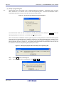
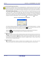
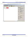
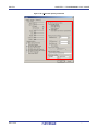
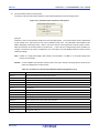
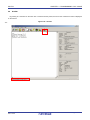
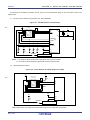
(1) Click the [Programmer] menu on the menu bar and select [Update Firmware]; the [Update Firmware] dialog box will
then be opened.
Figure 3-1. [Update Firmware] Command
<R>
Figure 3-2. [Update Firmware] Dialog Box
R20UT0008EJ0500 Rev. 5.00
2011.12.26
Page 30 of 254
PG-FP5
CHAPTER 3 SOFTWARE INSTALLATION
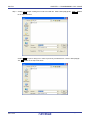
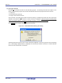
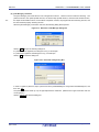
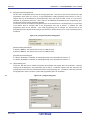
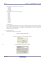
(2) Click the OK button to continue firmware update. The [Open firmware file] dialog box is opened.
Figure 3-3. [Open firmware file] Dialog Box
Select the firmware file “fp5_fw_vxxx.rec” and then click the Open button.
Cautions 1. Do not use FP5 firmware other than the one posted on the website; otherwise, a defect may
occur.
2. When a firmware of FP5 updates from V2.00 to V1.xx, a serial number of FP5 is erased.
And, FP5 can't operate in USB1.1. In addition, the other functions don't have any problem.
When FP5 revives, consult a Renesas Electronics sales representative or distributor.
R20UT0008EJ0500 Rev. 5.00
2011.12.26
Page 31 of 254
PG-FP5
CHAPTER 3 SOFTWARE INSTALLATION
(3) Some commands are sent to the FP5 and the update progress status is displayed in the action log window. The
message “Firmware Update succeeds”, which indicates normal completion of firmware update, and “Restarting
FP5..”, which is equivalent to [RESET] command processing, is automatically performed. The new version can
then be checked as “Firmware Version Vx.xx”. The update takes about 10 seconds.
Remark
The action log window is a part of the main window of the programming GUI, which shows the operation
progress status.
Figure 3-4. Action Log Window When Firmware Update Is Finished
<R>
Remark
Depending on the changes made, the following dialog box will be displayed. In this case, the information
stored in the FP5 (PR5 file, ESF file, program file) will have been deleted, so please download those files
again. (Refer to 4.2 Starting the Programming GUI.)
R20UT0008EJ0500 Rev. 5.00
2011.12.26
Page 32 of 254
PG-FP5
3.4.4
CHAPTER 3 SOFTWARE INSTALLATION
Installation of FPGA update
Install the latest FPGA by using the latest programming GUI. Decompress the file to any folder. The FPGA file
“fp5_fpga_vx.rec” will then be decompressed into the folder, so copy it to any folder. (“x” indicates the FPGA version.)
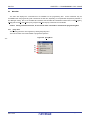
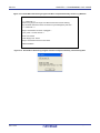
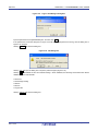
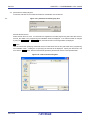
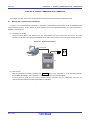
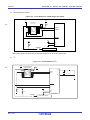
(1) Click the [Programmer] menu on the menu bar and select [Update FPGA]; the [Update FPGA] dialog box will then
be opened.
Figure 3-5. [Update FPGA] Command
<R>
Figure 3-6. [Update FPGA] Dialog Box
R20UT0008EJ0500 Rev. 5.00
2011.12.26
Page 33 of 254
PG-FP5
CHAPTER 3 SOFTWARE INSTALLATION
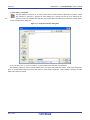
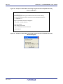
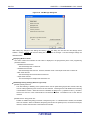
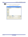
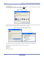
(2) Click the OK button to continue FPGA update. The [Open FPGA file] dialog box is opened.
Figure 3-7. [Open FPGA file] Dialog Box
Select the FPGA file “fp5_fpga_vx.rec” and then click the Open button.
Caution
Do not use an FP5 FPGA other than the one posted on the website; otherwise, a defect may
occur.
R20UT0008EJ0500 Rev. 5.00
2011.12.26
Page 34 of 254
PG-FP5
CHAPTER 3 SOFTWARE INSTALLATION
(3) Some commands are sent to the FP5 and the update progress status is displayed in the action log window. The
message “FPGA Update succeeded”, which indicates normal completion of firmware update, and “FP5 Power will
be switched OFF now.....”, which is equivalent to processing when the POWER button is turned off, is
automatically executed. The update takes about 30 seconds.
Figure 3-8. Action Log Window When FPGA Update Is Finished
<R>
(4) Click the OK button in the error message dialog box and then press the POWER button on the FP5 to turn on
power.
R20UT0008EJ0500 Rev. 5.00
2011.12.26
Page 35 of 254
PG-FP5
CHAPTER 3 SOFTWARE INSTALLATION
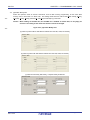
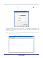
(5) Click the [Programmer] menu on the menu bar and select [Setup host connection...]; the [Host Connection] dialog
box will then be opened. Select the communication mode used and then click the OK button.
Figure 3-9. [Setup host connection] Command
<R>
Figure 3-10. [Host Connection] Dialog Box
R20UT0008EJ0500 Rev. 5.00
2011.12.26
Page 36 of 254
PG-FP5
CHAPTER 3 SOFTWARE INSTALLATION
(6) Communication with the host machine is established. “FPGA Vx” is displayed in the action log window; thus, the
version can be checked.
<R>
Figure 3-11. Version Confirmation After FPGA Update Is Finished
R20UT0008EJ0500 Rev. 5.00
2011.12.26
Page 37 of 254
PG-FP5
CHAPTER 4 PROGRAMMING GUI USAGE
CHAPTER 4 PROGRAMMING GUI USAGE
This chapter explains functional details on windows and dialog boxes of the programming GUI.
4.1
Introduction
Make sure that the programming GUI, USB driver, and the FP5 parameter file (PR5 file) for the target device are
installed. For the installation method, refer to CHAPTER 3 SOFTWARE INSTALLATION.
4.2
Startup of Programming GUI
(1) System connection
Connect a USB cable (or serial cable) to the USB port (or serial port) on the host machine, and the other side of the
cable to the USB connector (or serial connector) on the FP5. Plug in the AC adapter and then connect to the FP5
power supply connector.
Figure 4-1. System Connection
Serial cable
or
USB cable
AC adapter
Host
machine
Outlet
FP5
(2) FP5 startup
After the cables are connected, press the POWER button on the FP5. When the FP5 is correctly started, the
POWER LED is turned on and “Commands >” is displayed in the message display. If not, the cause may be a
defect in the FP5, so consult a Renesas Electronics sales representative or distributor.
R20UT0008EJ0500 Rev. 5.00
2011.12.26
Page 38 of 254
PG-FP5
CHAPTER 4 PROGRAMMING GUI USAGE
(3) Startup of programming GUI
<R>
Click the Start menu, “All Programs”, point to “Renesas Electronics CubeSuite+”, “Programming Tools”, and then
select “PG-FP5 Vx.xx” of “PG-FP5 Vx.xx” to start the Programming GUI.
The valid communication mode is
automatically detected in the order of the USB, and then the serial interface.
Figure 4-2. Port Scanning at Startup of Programming GUI
The communication mode can also be selected by cancelling this operation by clicking the Cancel button and
selecting the [Setup host connection...] command in the [Programmer] menu.
When communication is established and the programming GUI is correctly started, the main window will be opened.
Note that when the programming GUI is started for the first time, the valid programming area is cleared or once
FP5 unit from a number of units has been connected, the following message will be displayed, so download the
following ESF file, PR5 file or program file. This message means that ESF file and program file in the FP5 unit and
the information stored in the programming GUI (INI file) do not match.
Figure 4-3. Message Displayed at the First Startup of Programming GUI
Step 1. Click the OK button in the dialog box.
Step 2. The following dialog box will be displayed. Click Yes or No .
R20UT0008EJ0500 Rev. 5.00
2011.12.26
Page 39 of 254
PG-FP5
CHAPTER 4 PROGRAMMING GUI USAGE
Step 3. Clicking Yes will open a dialog box to make a new ESF file. Refer to 4.3.3 (15) (a) <3>
New… Button
for the steps that follow.
Clicking No will open a dialog box to select a previously created ESF file. Refer to 4.3.3 (15) (a)
<3> ... Button for the steps that follow.
R20UT0008EJ0500 Rev. 5.00
2011.12.26
Page 40 of 254
PG-FP5
CHAPTER 4 PROGRAMMING GUI USAGE
Step 4. Next, the device setup dialog box that is opened when [Device] menu -> [Setup...] command is executed
will be opened, so make the settings. Refer to 4.3.3 (15) [Setup...] command for the steps that follow.
Figure 4-4. Main Window
<R>
<1> Menu bar
<4> Programmer parameter window
<2> Toolbar
<3> Action log window
<6> Hint bar
<5> Status bar
The main window consists of the following areas.
Name
Displayed Items
Refer to:
<1>
Menu bar
Menu items executable by the programming GUI
4.3
<2>
Toolbar
Frequently used commands, as buttons
4.4
<3>
Action log window
A programming GUI action log
4.5
<4>
Programming parameter window
Programming parameter settings
4.6
<5>
Status bar
Command progress shown as a color or with a message
4.7
<6>
Hint bar
Hints for commands and toolbar
4.8
R20UT0008EJ0500 Rev. 5.00
2011.12.26
Page 41 of 254
PG-FP5
4.3
CHAPTER 4 PROGRAMMING GUI USAGE
Menu Bar
The menu bar displays the commands that are available for the programming GUI.
Some commands may be
unavailable when the programming GUI is started for the first time, depending on the parameter file (PR5 file) selected or
FP5 Manager setting. Also, if an HCUHEX file is selected, the HCUHEX file is handled as master data, so the [Program],
[Read], [Set Security], [Set Option bytes], and [Set OCD Security ID] commands are unavailable.
Caution
4.3.1
During command execution, do not execute other commands or terminate the programming GUI.
[File] menu
The following pull-down menu appears by clicking the [File] menu.
This menu includes commands related to program file operation.
Figure 4-5. [File] Menu
<R>
(1)
(2)
(3)
(4)
R20UT0008EJ0500 Rev. 5.00
2011.12.26
Page 42 of 254
PG-FP5
CHAPTER 4 PROGRAMMING GUI USAGE
(1) [Hex Editor...] command
The [Hex Editor] menu allows you to edit a program file in Intel HEX format or Motorola HEX format. When
this command is executed, a program file select dialog box is opened and the file to be edited can be
<R>
specified. Note that HCUHEX files, DDI files, and program files for the RX family, R8C family, SuperH family
cannot be loaded in this dialog box.
Figure 4-6. Program File Select Dialog Box
S-rec / Hex files (*.rec;*.s*;*.hex) or All files (*.*) may be selected from the Files of types list box.
After selecting a file to be opened, the file selected in the HEX Editor main window is loaded. At this time, whether the
file is of the Intel HEX format or Motorola HEX format is automatically recognized. When loading is finished, the HEX
Editor main window is opened.
R20UT0008EJ0500 Rev. 5.00
2011.12.26
Page 43 of 254
PG-FP5
CHAPTER 4 PROGRAMMING GUI USAGE
Figure 4-7. HEX Editor Main Window
Address display area
ASCII display area ID Tag area
Data display area
The displayed file contents can be modified by placing the pointer in the data display area in the HEX Editor main
window. Data input via the keyboard is accepted for all shown memory locations.
The ID Tag area is the area used with the target device supporting data flash. Only area indicating 0 or 1 can be edited
in this area. Input 0 or 1 for the ID Tag area. If 0 is input, then 00000000h will be set, and if 1 is input, FFFFFFFFh will be
used as the ID Tag. For details on data flash and ID tags, refer to the user’s manual of the target device.
The HEX Editor only accepts hexadecimal data, i.e., numbers 0 to 9 and letters A to F. All other data will be rejected.
The ASCII representation, if any, is shown in the ASCII display area. This area is for reference only, so no data can be
input.
Use the scroll bar to move another address range into the visible area of the HEX Editor.
The following keys can be input using the keyboard.
Table 4-1. Key Functions That Can Be Input in HEX Editor Window
Key
0-9, A-F
Function
Data input (data display area)
Move cursor in right direction
Move cursor in left direction
Move cursor in up direction
Move cursor in down direction
Tab
Tab Move cursor to next input field (address + 1)
If any changes have been made to the file, [Save] and [Save As] in the [File] menu in the HEX Editor main window
become available for saving the modified data.
The [Save As] display varies whether or not the downloaded PR5 file is for the target device that supports data flash.
R20UT0008EJ0500 Rev. 5.00
2011.12.26
Page 44 of 254
PG-FP5
CHAPTER 4 PROGRAMMING GUI USAGE
Figure 4-8. [Save As] Dialog Box of HEX Editor
(a) The downloaded PR5 file is for a target device that does not support data flash
(b) The downloaded PR5 file is for a target device that supports data flash
R20UT0008EJ0500 Rev. 5.00
2011.12.26
Page 45 of 254
PG-FP5
CHAPTER 4 PROGRAMMING GUI USAGE
Besides the file name and folder location, a start address and an end address for the new file can be selected in the
[Save As] dialog box. The original start address and end address are displayed by default. Select the file radio button for
the format in which to save the data. Select the same format as that of the loaded file. Use of the saved file with other tool
products is not supported.
<R>
Remark
In a microcontroller that supports ID Tags of data flash, for the saved program file contents of the data flash
area, refer to Figure B-1 Relationship Between HEX Editor and Saved Program File.
(2) [Upload from FP5...] command
The [Upload from FP5...] command is used to upload the program file, PR5 file and ESF file saved in a valid
programming area.
Figure 4-9. [Upload from FP5...] Dialog Box in the HEX Editor (1/2)
<R>
(a) When a product without data flash is selected from the 78K, V850, RL78 family
<1>
<2>
<3>
<4>
R20UT0008EJ0500 Rev. 5.00
2011.12.26
Page 46 of 254
PG-FP5
CHAPTER 4 PROGRAMMING GUI USAGE
Figure 4-9. [Upload from FP5...] Dialog Box in the HEX Editor (2/2)
(b) When a product with data flash is selected from the 78K, V850, RL78 family
<R>
<1>
<2>
<3>
<4>
(c) When the RX family, R8C family, or SuperH family is selected
<R>
<1>
<2>
<3>
<4>
<1> [Upload program file from FP5] button
The storage location and file name of the program file are specified in the HEX file: box. In order to change the file
location or name, click the Save as button and make the changes.
<2> [Upload Parameter/Setting files from FP5] button
The Parameter file: box specifies the storage location of the PR5 file. The Setting file: box specifies the ESF file
storage location and file name. In order to change the file locations, click the Save as button and make the
changes. The parameter file names cannot be changed.
R20UT0008EJ0500 Rev. 5.00
2011.12.26
Page 47 of 254
PG-FP5
CHAPTER 4 PROGRAMMING GUI USAGE
<3> Address range selection area
This area is enabled with the [Upload program file from FP5] button clicked. Specify the address range of the
program file that is to be saved. When a product with data flash is selected from the 78K, V850, RL78 family,
<R>
[Code flash:] and [Data flash:] are displayed. For the RX family, R8C family, and SuperH family, [User mat], [Data
mat], and [User boot] are displayed.
<4> Option area
When the [Show data] check box is checked, the action log window will be displayed when the upload is executed.
Pressing the OK button will start the upload with the selected settings.
Pressing the Cancel button will close the dialog box without executing the upload.
(3) [Checksum] command
The [Checksum] command calculates the checksum of the selected program file downloaded to FP5 and displays
the result. When this command is executed, the Checksum dialog box appears. Select the optional calculation
method and the target address range, and click the OK button. The result will then be displayed in the [File
Checksum] area in the action log window and programmer parameter window. This command can be executed
after the [Setup] command is executed. If the [Setup] command is executed again after the [Checksum] command
is executed, the result displayed in the [File Checksum] area in the programmer parameter window will be cleared.
Figure 4-10. Checksum Dialog Box
<R>
(a) When a product without data flash is selected
from the 78K, V850, RL78 family
<1>
(b) When a product with data flash is selected from the 78K,
V850, RL78 family
<1>
<2>
<2>
<3>
R20UT0008EJ0500 Rev. 5.00
2011.12.26
<3>
Page 48 of 254
PG-FP5
CHAPTER 4 PROGRAMMING GUI USAGE
(c) When the RX family, R8C family, or SuperH family is selected
<R>
<1>
<2>
<3>
<1> Programming area
The valid programming area is displayed.
<R>
<2> Checksum calculation mode selection
Select the mode for calculating checksum of the selected program file.
Arithmetic checksum (16bit): 16-bit arithmetic (subtraction)
Arithmetic checksum:
32-bit arithmetic (addition)
CRC sum (32bit):
32-bit CRC
Remark
With the 16-bit arithmetic (subtraction) mode, the lower 4 digits of the result from which a value is subtracted
from 00h in 1-byte units are displayed.
With the 32-bit arithmetic (addition) mode, the lower 8 digits of the result to which a value is added from 00h
in 1-byte units are displayed.
With 32-bit mode, the 8-digit result of CRC32 function calculation is displayed. For details on arithmetic
specifications, refer to Figure B-2 32-bit CRC Calculation Specifications.
The 16-bit arithmetic (subtraction) mode can be selected when the 78K, V850, or RL78 family is selected.
The 32-bit arithmetic (addition) mode can be selected when the RX family, R8C family, or SuperH family is
selected.
R20UT0008EJ0500 Rev. 5.00
2011.12.26
Page 49 of 254
PG-FP5
CHAPTER 4 PROGRAMMING GUI USAGE
<3> Address range selection
Select the range for calculating checksum of the selected program file. If there is no program file data in the
<R>
specified range, the specified range is filled with FFh for calculation. When a product with data flash is selected
from the 78K, V850, RL78 family, [Code flash:] and [Data flash:] are displayed. When the RX family, R8C family, or
SuperH family is selected, [User mat], [Data mat], and [User boot] are displayed.
Device Area:
From the start to end addresses of the device, which are contained in the selected PR5 file
User Defined: Any range can be specified by inputting the addresses to the [Start Address] and [End Address]
text boxes.
Clicking the OK button displays the calculation result in the [File Checksum] area in the action log window and
programmer parameter window.
Clicking the Cancel button closes the dialog box without saving the settings made in the Checksum dialog box.
Remark
When the valid programming area is changed or a program file is downloaded, the checksum result will
be cleared.
<R>
Figure 4-11. Checksum Result <When Product without Data Flash Is Selected from 78K, V850, RL78 Family>
R20UT0008EJ0500 Rev. 5.00
2011.12.26
Page 50 of 254
PG-FP5
CHAPTER 4 PROGRAMMING GUI USAGE
Figure 4-12. Checksum Result
<R>
(a) When Product with Data Flash Is Selected from 78K, V850 or RL78 Family
(b) When RX Family, R8C Family or SuperH Family Is Selected
(4) [Quit] command
The [Quit] command terminates the programming GUI. The programming GUI can also be terminated by clicking
the button on the right end of the title bar in the main window. When the programming GUI is terminated,
various settings are saved in the INI file (FP5.ini), and these settings are loaded when the programming GUI is
<R>
started the next time.
R20UT0008EJ0500 Rev. 5.00
2011.12.26
Page 51 of 254
PG-FP5
4.3.2
CHAPTER 4 PROGRAMMING GUI USAGE
[Programmer] menu
Clicking the [Programmer] menu displays the following pull-down menu.
This menu includes commands related to FP5 settings.
Figure 4-13. [Programmer] Menu
<R>
(1)
(2)
(3)
(4)
(5)
(6)
(7)
(8)
(9)
(1) [Setup host connection] command
Running the [Setup host connection] command opens the [Host Connection] dialog box.
The channel for
communication between the FP5 and the host machine can be selected and configured in this dialog box.
Figure 4-14. [Host Connection] Dialog Box
“USB” can be selected as the communication channel if the USB interface is supported in the PC used.
When selecting “Serial”, select the COM port and baud rate from the drop-down list boxes. COM ports that are
recognized by the host machine are displayed in the Port list. Up to 256 ports can be recognized.
When the OK button is clicked, software tries to establish a connection between the FP5 and the host machine
using the selected communication channels.
Clicking the Cancel button closes the window without making any changes.
R20UT0008EJ0500 Rev. 5.00
2011.12.26
Page 52 of 254
PG-FP5
CHAPTER 4 PROGRAMMING GUI USAGE
(2) [Logging] command
The [Logging] command saves information displayed in the action log window in the log file. When this command
is executed, the log file save dialog box appears. Move to an arbitrary folder, select the log file in the [File name]
drop-down list, and click the Save button; the log file will then be saved. The [Logging] command on the menu
bar will be checked. The check mark will be cleared by clicking the [Logging] command again and saving of the log
file will be stopped. Enabling/disabling the [Logging] command is added to the time stamp. For a log file example,
refer to Figure B-3 Log File Example.
Remark
The log file that was saved the last time is displayed in the log file save dialog box.
Figure 4-15. Log File Save Dialog Box
Clicking the Save button saves the specified log file.
Clicking the Cancel button closes the dialog box without saving the log file.
R20UT0008EJ0500 Rev. 5.00
2011.12.26
Page 53 of 254
PG-FP5
CHAPTER 4 PROGRAMMING GUI USAGE
(3) [Select Programming area] command
The FP5 has a 16 MB flash memory area for saving program files. This memory area can be used as four 4 MB
programming areas (Area 0 to Area 3) or eight independent 2 MB programming areas (Area 0 to Area 7). Program
files can be downloaded to each programming area, and which file, PR5 or ESF, is to be saved is selectable in
programming area units. That is, files can be individually downloaded in each programming area, and the area
used can also be selected individually.
This command is used to select a valid programming area from the FP5’s four (or eight) programming areas (4 MB
in case of four areas, or 2 MB in case of eight areas). When this command is executed, the programming area
select dialog box is opened, and the desired programming area can be selected. The number of programming
areas that can be selected with this command is the value defined in the [Programming Area Setting] area on the
[Target] tab of the Device Setup dialog box, which is opened by the [Setup...] command in the [Device] menu.
Figure 4-16. Programming Area Select Dialog Box
The currently selected programming area is displayed in the programming area selection dialog box. To change
the area, select the relevant number from the list box and click the OK button. To check the contents set to each
area or to change the division factor, see the [Target] tab of the Device Setup dialog box.
Clicking the OK button selects the programming area selected in the programming area select dialog box.
Clicking the Cancel button closes the dialog box without changing the programming area.
(4) [Buzzer] command
The [Buzzer] command is used to enable or disable the setting to output the buzzer sound from the FP5 main unit.
When this command is executed, the [Buzzer] command on the menu bar is checked and becomes valid. When
this command is executed again, the check mark is cleared and the command becomes invalid. The FP5 makes a
double-beep sound when the Autoprocedure(E.P.) command is completed normally, or makes a buzzer sound
when the command is completed abnormally.
(5) [Reset] command
When the [Reset] command is executed, a software reset can be applied to the FP5. After reset, the current
versions of the firmware, FPGA, the FP5 serial number, and mode will be displayed in the action log window.
R20UT0008EJ0500 Rev. 5.00
2011.12.26
Page 54 of 254
PG-FP5
CHAPTER 4 PROGRAMMING GUI USAGE
(6) [Self-Test] command
The [Self-Test] command executes the FP5 self-testing program. The following three items are subject to selftesting. The self-testing program does not affect the PR5 files, ESF files and program files saved in the FP5.
<1> FPGA test
<2> Power generation block test
<3> Target / remote interface I/O test
Since execution of the [Self-Test] command involves I/O testing, a message that prompts the user to disconnect
hardware connected the target connector or remote connector is displayed. Remove hardware (including target
system and program adapter), connected to the target connector or remote connector, if any. Make sure that no
hardware is connected and click the OK button; self-testing will then be executed.
If the Cancel button is clicked, self-testing will not be executed.
Figure 4-17. Confirmation Before Starting Self-Testing
Self-testing takes about three seconds, and the result will be displayed in the action log window and a result dialog
box. If the message “Selftest FAILED.” is displayed, the cause may be a defect in the FP5, so consult a Renesas
Electronics sales representative or distributor.
R20UT0008EJ0500 Rev. 5.00
2011.12.26
Page 55 of 254
PG-FP5
CHAPTER 4 PROGRAMMING GUI USAGE
Figure 4-18. Result When Self-Testing Program Has Been Completed Normally <Action Log Window>
>selftest
***** CAUTION *****
Remove any plugs from Target- and Remote-Connector before starting.
Any hardware attached to those connectors may be damaged by this test !
***** CAUTION *****
Target- and Remote-connector unplugged ?
If yes, press 's' to start the test: s
FPGA Test: PASS
Power Supply Test: PASS
Target- and Remote-Interface Test: PASS
Selftest PASSED.
>
Figure 4-19. Result When Self-Testing Program Has Been Completed Normally <Result Dialog Box>
R20UT0008EJ0500 Rev. 5.00
2011.12.26
Page 56 of 254
PG-FP5
CHAPTER 4 PROGRAMMING GUI USAGE
Figure 4-20. Example of Result When Self-Testing Program Has Been Completed Abnormally
<Action Log Window>
>selftest
***** CAUTION *****
Remove any plugs from Target- and Remote-Connector before starting.
Any hardware attached to those connectors may be damaged by this test !
***** CAUTION *****
Target- and Remote-connector unplugged ?
If yes, press 's' to start the test: s
FPGA Test: PASS
Power Supply Test: PASS
Target- and Remote-Interface Test: FAIL
Selftest FAILED.
>
Figure 4-21. Example of Result When Self-Testing Program Has Been Completed Abnormally
<Result Dialog Box>
R20UT0008EJ0500 Rev. 5.00
2011.12.26
Page 57 of 254
PG-FP5
CHAPTER 4 PROGRAMMING GUI USAGE
(7) [Update Firmware] command
The [Update Firmware] command updates the firmware. Refer to 3.4 Updating Programming GUI, Firmware
and FPGA and download the relevant update file before starting update.
Executing of this command displays the following dialog box.
Figure 4-22. [Update Firmware] Dialog Box
To continue the firmware update, click the OK button.
Clicking the Cancel button cancels the firmware update.
Clicking the OK button opens the [Open firmware file] dialog box.
Figure 4-23. [Open firmware file] Dialog Box
Select the firmware file “fp5_fw_vxxx.rec” and then click the Open button.
Cautions 1. Do not use FP5 firmware other than the one posted on the website; otherwise, a defect may
occur.
2. When a firmware of FP5 updates from V2.00 to V1.xx, a serial number of FP5 is erased.
And, FP5 can't operate in USB1.1. In addition, the other functions don't have any problem.
When FP5 revives, consult a Renesas Electronics sales representative or distributor.
R20UT0008EJ0500 Rev. 5.00
2011.12.26
Page 58 of 254
PG-FP5
CHAPTER 4 PROGRAMMING GUI USAGE
Some commands are sent to the FP5 and the update progress status is displayed in the action log window. The
message “Firmware Update succeeds”, which indicates normal completion of firmware update, and “Restarting
FP5...”, which is equivalent to [RESET] command processing, is automatically performed. The new version can
then be checked as “Firmware Version Vx.xx”. The update takes about 10 seconds.
Figure 4-24. Action Log Window When Firmware Update Is Finished
<R>
Remark
Depending on the changes made, the following dialog box will be displayed.
In this case, the
information stored in the FP5 (PR5 file, ESF file, program file) will have been deleted, so please
download those files again. (Refer to 4.2 Starting the Programming GUI.)
R20UT0008EJ0500 Rev. 5.00
2011.12.26
Page 59 of 254
PG-FP5
CHAPTER 4 PROGRAMMING GUI USAGE
(8) [Update FPGA] command
The [Update FPGA] command updates the FPGA. Refer to 3.4 Updating Programming GUI, Firmware and
FPGA and download the relevant update file before starting update.
Executing of this command displays the following dialog box.
Figure 4-25. [Update FPGA] Dialog Box
To continue the FPGA update, click the OK button.
Clicking the Cancel button cancels the FPGA update.
Clicking the OK button opens the [Open FPGA file] dialog box.
Figure 4-26. [Open FPGA file] Dialog Box
Select the FPGA file “fp5_fpga_vx.rec” and then click the Open button.
Caution
Do not use FP5 FPGA other than the one posted on the website; otherwise, a defect may occur.
R20UT0008EJ0500 Rev. 5.00
2011.12.26
Page 60 of 254
PG-FP5
CHAPTER 4 PROGRAMMING GUI USAGE
Some commands are sent to the FP5 and the update progress status is displayed in the action log window. The
message “FPBGA Upload succeeded.”, which indicates normal completion of firmware update, and “FP5 Power will
be switched OFF now.....”, which is equivalent to processing when the POWER button is turned off, is
automatically executed. The update takes about 30 seconds.
Figure 4-27. Action Log Window When FPGA Update Is Finished
<R>
Click the OK button in the error message dialog box and then press the POWER button on the FP5 to turn on
power.
Execution of the [Setup host connection...] command opens the [Host Connection] dialog box.
Select the
communication mode used and then click the OK button.
R20UT0008EJ0500 Rev. 5.00
2011.12.26
Page 61 of 254
PG-FP5
CHAPTER 4 PROGRAMMING GUI USAGE
Figure 4-28. [Setup host connection] Command
<R>
Figure 4-29. [Host Connection] Dialog Box
The main window is opened. “Board H/W V1, FPGA Vx” is displayed in the action log window; thus, the version
can be checked.
R20UT0008EJ0500 Rev. 5.00
2011.12.26
Page 62 of 254
PG-FP5
<R>
CHAPTER 4 PROGRAMMING GUI USAGE
Figure 4-30. Version Confirmation After FPGA Update Is Finished
R20UT0008EJ0500 Rev. 5.00
2011.12.26
Page 63 of 254
PG-FP5
CHAPTER 4 PROGRAMMING GUI USAGE
(9) [FP5 Manager] command
The [FP5 Manager] command sets the FP5 management functions. These functions include the following: The
password function, the upload prohibit function, the device setup prohibit function, the bank mode enable function,
<R>
the simple mode enable function, the checksum comparison function, the program file size monitoring function, and
the reset terminal property switching function.
When the [FP5 Manager] command is executed, the following dialog will be opened.
Figure 4-31. Welcome to FP5 Manager Dialog Box
Clicking Yes will open the following dialog box.
If a password is not registered, the dialog box in Fig. 4-32 will open.
If a password is registered, the dialog box in Fig. 4-33 will open.
Clicking No will close the dialog box.
Figure 4-32. Password setting Dialog Box
In order to register a password, input a password into the [PASSWORD] box and [Confirm PASSWORD] box, and
then click OK .
The password must be made up of up to eight alphanumeric characters. (Differences in upper and lower case are
not recognized.)
Clicking Cancel will close the dialog box.
R20UT0008EJ0500 Rev. 5.00
2011.12.26
Page 64 of 254
PG-FP5
CHAPTER 4 PROGRAMMING GUI USAGE
Figure 4-33. Login to FP5 Manager Dialog Box
Input the password into the [PASSWORD] box, and then click OK .
If the password is correct the dialog box in Figure 4-35 will open. If the password is wrong, then the dialog box in
Figure 4-34 will open.
Clicking Cancel will close the dialog box.
Figure 4-34. FP5 Dialog Box
Clicking Yes will open the dialog box to input the password again (Figure 4-33).
Clicking No will initialize the FP5 to its default settings. When initialized, the following stored information will be
deleted or reset to their defaults:
Password
FP5 Manager setting
PR5 file
ESF file
Program file
Clicking Cancel will close the dialog box.
R20UT0008EJ0500 Rev. 5.00
2011.12.26
Page 65 of 254
PG-FP5
CHAPTER 4 PROGRAMMING GUI USAGE
Figure 4-35. FP5 Manager Dialog Box
After making any changes to the settings and clicking OK , the dialog box will close and the settings will be
enabled. Clicking Cancel will close the dialog box and discard the changes. The FP5 Manager settings are
described below.
Displaying Mode Contents
The mode contents that indicate the FP5 state is displayed in the [Programmer] area of the programming
parameter window.
- Standard mode unsecured
The FP5 Manager has not been set.
- Standard mode secured
The FP5 Manager has been set. However, the bank mode or the simple mode have not been set.
- Bank mode secured
The FP5 Manager and bank mode have been set.
- Simple mode secured
The FP5 Manager and simple mode have been set.
FP5 Manager Dialog Settings (Refer to Figure 4-35)
[Disable Upload] check box
This sets enabling or disabling of the upload function used to upload data (program file, PR5 file, ESF file)
from the valid programming area of FP5 to the host machine. Checking the box will disable and unchecking
it will enable the function. When this function is disabled, the [File] menu -> [Upload from FP5...] command,
and the hex and srec of the communications command are disabled. The default is not to have this box
checked.
[Disable Device Setup] check box
Enables or disables the [Setup] command in the [Device] menu. It is disabled when checked, and enabled
when not checked. When it is disabled, the [Setup] command in the [Device] menu, as well as the downprm,
downset, and lod communication commands become invalid.
R20UT0008EJ0500 Rev. 5.00
2011.12.26
Page 66 of 254
PG-FP5
CHAPTER 4 PROGRAMMING GUI USAGE
[Enable Bank mode] check box
Sets the normal mode or bank mode for the mode of the remote connector. Checking this box will set the
bank mode, and not checking it will set the normal mode. If checked, [Enable Simple mode] cannot be
checked. When in the bank mode, the programming area can be selected through the remote connector.
With respect to detailed functions, refer to CHAPTER 7 USAGE THE REMOTE CONNECTOR. The default
is not to have this box checked.
[Enable Simple mode] check box
Sets the normal mode or the simple mode. Checking this box will set the simple mode, and not checking it
will set the normal mode. If checked, [Enable Bank mode] cannot be checked. When in the simple mode,
the functions of the FP5 control buttons and message display will change. When
the NEXT button is clicked, the programming area will be switched. Clicking the ENTER button
or START button will execute the Autoprocedure(E.P.) command. The message display will display (1) the
programming area number, (2) the program file name, and (3) the checksum and (4) command name.
Immediately after the program file is downloaded, the checksum will show H:xxxxxxxx. At this time, the
program file will be checked using 32-bit CRC calculations from the start to the end address. After this,
executing [File] menu -> [Checksum] command will display F:xxxxxxxx. The default is not to have this box
checked.
Figure 4-36. Example of Message Display
(1)
(3)
(2)
0:sample.hex
H:AFE33BC0 E.P.>
(4)
[Checksum comparison] check box
When [Device] menu -> [Checksum] command is executed and the checksum of the target device is
displayed, the checksum of the program file stored in FP5 will be referenced and the results displayed.
Checking this box will cross-reference the checksum, and not checking it will not. The default is not to have
this box checked.
Figure 4-37. Example of Action Log Window
>Sum
Checksum: 0x623E
Checksum compare: PASS
Checksum operation: finished.
[Program file size monitor function ] check box
Halts execution of programming commands if the program file size exceeds the programmable range. If this
check box is checked and the address range of the downloaded program file exceeds the address range
specified in the [Operation Mode] area on the [Standard] tab of the Device Setup dialog box, executing a
[Program], [Verify], or [Autoprocedure(E.P.)] command will cause the error message “ERROR (E302): Hex
file exceeds target device flash range.” to appear in the Action Log window and execution of the command
will halt. If this check box is not checked, the warning message “WARNING: HEX file exceeds target device
flash range.” will appear in the Action Log window, but execution of the command will continue. The default
is not to have this box checked.
R20UT0008EJ0500 Rev. 5.00
2011.12.26
Page 67 of 254
PG-FP5
CHAPTER 4 PROGRAMMING GUI USAGE
[Reset option of Run after Disconnect]
When the [Run after Disconnect] function in the [Command options] area of the Device setup dialog
¯¯¯¯¯¯ signal after the write command is completed can be
[Advanced] tab is enabled, the properties of the RESET
set to Pull-up or Hi-Z. The default is Hi-Z.
[Change the PASSWORD] button
Clicking the [Change the PASSWORD] button will open the following dialog box.
Figure 4-38. Password setting Dialog Box
This dialog box allows the user to change the registered password.
Input the current password into the [OLD PASSWORD] box, input the new password into the [NEW
PASSWORD] box and [Confirm PASSWORD] box, and then click OK . When Cancel is clicked, the
dialog box will be closed and the password will not be changed.
[INIT] button
Resets the FP5 to its default settings. Initializing the FP5 will reset or delete the following stored information.
Password
FP5 Manager setting
PR5 file
ESF file
Program file
R20UT0008EJ0500 Rev. 5.00
2011.12.26
Page 68 of 254
PG-FP5
4.3.3
CHAPTER 4 PROGRAMMING GUI USAGE
[Device] menu
The following pull-down menu appears by clicking the [Device] menu.
This menu includes commands mainly related to programming to the target device, such as erase, write and verify.
Figure 4-39. [Device] Menu
(a) When 78K, V850, RL78 Family Is Selected
(1)
(2)
(3)
(4)
(5)
(6)
(7)
(8)
(9)
(10)
(12)
(13)
(14)
(15)
(b) When RX Family, R8C Family or SuperH Family Is Selected
<R>
(1)
(2)
(3)
(4)
(5)
(7)
(8)
(11)
(12)
(13)
(15)
(1) [Blank check] command
The [Blank Check] command performs blank check for the flash memory in the target device. The target area can
be set in the [Operation Mode] area on the [Standard] tab in the Device Setup dialog box. If the flash memory has
already been erased, “PASS” is displayed. If the flash memory has not yet been erased, “ERROR” is displayed. If
this error is displayed, erase the entire area of the flash memory before starting programming.
R20UT0008EJ0500 Rev. 5.00
2011.12.26
Page 69 of 254
PG-FP5
CHAPTER 4 PROGRAMMING GUI USAGE
(2) [Erase] command
The [Erase] command erases the flash memory in the target device. The target area can be set in the [Operation
Mode] area on the [Standard] tab in the Device Setup dialog box. If this command is executed with [Chip] selected,
security command options are initialized at the same time. While erasing the flash memory is in progress, the
progress status is displayed in the action log window. When execution of this command is completed, the result of
command execution in the target device is displayed. Whether to perform the [Blank Check] command before
executing this command depends on the [Blank check before Erase] check box setting in the [Command options]
area on the [Advanced] tab in the Device Setup dialog box. If this command is executed for the target device that
has already been erased with the [Blank check before Erase] check box selected, “OK, Erase skipped.” is
displayed and erasure is not performed.
(3) [Program] command
The [Program] command transmits the memory contents (program files) in the FP5 valid programming area to the
target device and writes the programs to the flash memory. The target area can be set in the [Operation Mode]
area on the [Standard] tab in the Device Setup dialog box. The progress status of this command is displayed as a
percentage in the action log window. When execution of this command is completed, the programming GUI
displays the result of command execution in the target device. Command options after execution of this command
depend on the settings of the [Verify after Program], [Security after Program] and [Checksum after Program] check
boxes in the [Command options] area on the [Advanced] tab in the Device Setup dialog box. For details on these
check boxes, refer to 4.3.3 (15) (c) <2> [Command options] area.
<R>
(4) [Verify] command
For the 78K, V850, and RL78 family, the [Verify] command transmits the memory contents (program files) in the
FP5 valid programming area to the target device, verifies the data written to the flash memory in the target device,
and receives the result. For the RX family, R8C family, and SuperH family, it reads data from the microcontroller,
and compares it with the memory content (program file) in the effective programming area of the FP5. The target
area can be set in the [Operation Mode] area on the [Standard] tab in the Device Setup dialog box. The progress
status of this command is displayed as a percentage in the action log window. When execution of this command is
completed, the programming GUI displays the result of command execution in the target device.
<R>
(5) [Read] command
The [Read] command loads data on the flash memory in the target device and saves it as a file. The target range
of the flash memory is specified in the [Operation Mode] area on the [Standard] tab of the Device Setup dialog box.
When the [View] command is executed following this command, 4 KB read data is displayed in the log window
each time the ENTER key is pressed. When the [Write Intel HEX file] or [Write Motorola SREC file] command is
executed following this command, the read data can be saved in the Intel HEX format or Motorola HEX format.
Use of the saved file with other tool products is not supported.
Remark
The folder in which program data was saved the last time is displayed in the program data save dialog
box.
R20UT0008EJ0500 Rev. 5.00
2011.12.26
Page 70 of 254
PG-FP5
CHAPTER 4 PROGRAMMING GUI USAGE
Figure 4-40. Program Data Saved Dialog Box <When Write Intel HEX file Command Is Executed>
Figure 4-41. Program Data Save Dialog Box <When Write Motorola SREC file Command Is Executed>
Clicking the Open button saves the program data into a file and closes the dialog box.
Clicking the Cancel button closes the program data save dialog box without saving the program data into a file.
R20UT0008EJ0500 Rev. 5.00
2011.12.26
Page 71 of 254
PG-FP5
CHAPTER 4 PROGRAMMING GUI USAGE
(6) [Set Security] command
The [Set Security] command sets the security functions for the target device. When this command is executed, the
settings made in the [Set Security command options] area on the [Advanced] tab in the Device Setup dialog box
will be reflected in the target device. For details on the security functions, refer to 4.3.3 (15) (c) <4> [Set Security
command options] area.
<R>
(7) [Checksum] command
For the 78K, V850, RL78 family, RX family, and SuperH family, the [Checksum] command reads the checksum
calculated in the target device and displays it in the action log window. When using a 78K0S/Kx1+ microcontroller
or the PD78F9334, this command also displays the checksum of the program file and compares both. For the
R8C family, it reads the content of the flash memory of the target device, and displays the checksum calculated in
the FP5 on the action log window.
Remark
The checksum read by this command differs from the one displayed in the [File checksum] area in the
programmer parameter window.
For details on the [File checksum] area, refer to 4.3.1 (3)
[Checksum...] command.
The checksum is calculated as follows.
Note that this is the result when the [Enable Checksum Compare
Function] check box of the FP5 management Setting (M) dialog box is not selected.
<When using 78K (other than 78K0S/Kx1+, PD78F9334), V850E1, V850ES, RL78 family>
Method: Subtraction (16-bit arithmetic)
Range:
Area set in the [Operation Mode] area on the [Standard] tab in the Device Setup dialog box
Figure 4-42. Action Log Window After [Checksum] Command Execution
<When using 78K (Other than 78K0S/Kx1+, PD78F9334), V850E1, V850ES, RL78 Family>
>sum
Code flash: 0x8FCD
Data flash: 0x1000
Total:
0x9FCD
PASS
Checksum operation finished.
>
Remark
With the 16-bit arithmetic (subtraction) mode, the lower 4 digits of the result from which a value is
subtracted from 00h in 1-byte units are displayed.
R20UT0008EJ0500 Rev. 5.00
2011.12.26
Page 72 of 254
PG-FP5
CHAPTER 4 PROGRAMMING GUI USAGE
<When using a 78K0S/Kx1+ microcontroller or PD78F9334>
Method: Division (original)
Range:
Area set in the [Operation Mode] area on the [Standard] tab in the Device Setup dialog box
Figure 4-43. Action Log Window After [Checksum] Command Execution
(When using 78K0S/Kx1+ microcontroller or PD78F9334)
>sum
Device Checksum: 0x1842
FP5 Checksum: 0x1842
Checksum compare: PASS
Checksum operation finished.
>
Remark
For details on the arithmetic specifications, refer to Figure B-4
Division (Original) Calculation
Specifications.
<V850E2>
Method: 32-bit CRC
Range:
Area specified in the [Operation Mode] area on the [Standard] tab in the Device Setup dialog box
Figure 4-43. Action Log Window After [Checksum] Command Execution
(V850E2)
>sum
Code flash: 0x370A7BE5
Data flash: 0xBFD1B03F
Total: 0xF6DC2C24
PASS
Checksum operation finished.
>
Remark
32-bit CRC displays the 8-digit result of CRC32 function operation. For the calculation specifications,
refer to Figure B-2 32-bit CRC Calculation Specifications in APPENDIX B SUPPLEMENTARY
INFORMATION.
R20UT0008EJ0500 Rev. 5.00
2011.12.26
Page 73 of 254
PG-FP5
CHAPTER 4 PROGRAMMING GUI USAGE
<RX family, R8C family, SuperH family>
Method: 32-bit arithmetic (addition) mode
Range:
Result of calculating all the areas (user mat, data mat, user boot) selected in the [Operation Mode] area
on the [Standard] tab of the Device Setup dialog box
Figure 4-43. Action Log Window After [Checksum] Command Execution
(RX Family, R8C Family, SuperH Family)
>sum
User mat:
0x03FC0000
Data mat:
0x00444588
User Boot mat: 0x003FC000
Total:
0x04800588
PASS
Checksum operation finished.
>
Remark
With the 32-bit arithmetic (addition) mode, the lower 8 digits of the result to which a value is added from
00h in 1-byte units are displayed.
(8) [Autoprocedure(E.P.)] command
The [Autoprocedure(E.P.)] command executes the [Erase] and [Program] commands in succession. Exiting from
the flash memory programming mode is not possible between the [Erase] and [Program] commands. The target
area can be set in the [Operation Mode] area on the [Standard] tab in the Device Setup dialog box. The progress
status of this command is displayed in the action log window. When execution of this command is completed, the
programming GUI displays the result of command execution in the target device.
Command options after
execution of this command depend on the settings of the [Blank check before Erase], [Verify after Program],
[Security after Program], and [Checksum after Program] check boxes in the [Command options] area on the
[Advanced] tab in the Device Setup dialog box. For details on these check boxes, refer to 4.3.3 (15) (c) <2>
[Command options] area.
Figure 4-44. Action Log Window After [Autoprocedure(E.P.)] Command Execution
>ep
Blank check Chip:
PASS, Erase skipped.
Program Chip:
10%
20%
30%
40%
50%
60%
70%
80%
90%
100%
PASS
Erase, Program operation finished.
>
R20UT0008EJ0500 Rev. 5.00
2011.12.26
Page 74 of 254
PG-FP5
CHAPTER 4 PROGRAMMING GUI USAGE
(9) [Set Option bytes] command
The [Set Option bytes] command specifies the settings for the target device's option byte. When this command is
executed, the settings specified in the [Option byte setting] area on the [Advanced] tab of the Device Setup dialog
box are applied to the target device. For details of the option byte settings, see 4.3.3 (15) (c) <9> [Option byte
setting] area.
(10) [Set OCD Security ID] command
The [Set OCD Security ID] command specifies the settings for the target device's option byte.
When this
command is executed, the settings specified in the [OCD ID setting] area on the [Advanced] tab of the Device
Setup dialog box are applied to the target device. For details of the OCD security ID settings, see 4.3.3 (15) (c)
<8> [OCD ID setting] area.
<R>
(11) [Set Lock bits] command
The [Set Lock bits] command specifies the lock bits of the target device. When this command is executed, the
settings specified in the [Set Lock bits] area on the [Advanced] tab in the Device Setup dialog box are reflected to
the target device. For detais about lock bit settings, refer to 4.3.3 (15) (c) <10> [Set Lock bits] area.
(12) [Connect] command
Executes the con command or dcon command. When the con command is executed a check will be added and
when the dcon command is executed the check will be removed. When “autocon off” or “autocon on” is executed
with the autocon command, the [connect] command is enabled or disabled. Refer to CHAPTER 8
USAGE
COMMUNICATION COMMANDS for details about the functions.
(13) [Signature read] command
The [Signature read] command reads target device product information, such as the device name and flash
memory information.
The read result is displayed in the action log window.
<R>
(14) [Get Flash options] command
The [Get Flash options] command reads the settings for the flash options for the target device and displays the
result in the [Flash options] area on the [Advanced] tab in the Device Setup dialog box. When execution of this
command is enabled, execute this command before the [Set Security] command, [Set Option bytes] command, or
[Set OCD Security ID] command; the settings for the security functions or the boot area can thus be checked. For
details on the flash option settings, refer to 4.3.3 (15) (c) <3> [Flash options] area.
Caution
When loading an HCUHEX file, the HCUHEX file is handled as master data, so even though the
flash option settings specified for the device can be checked by executing the [Get Flash
Options] command, these settings cannot be applied to the device. The OK button in the
Device Setup dialog box is therefore unavailable. In this case, click the Cancel button and
close the Device Setup dialog box. Note that the OK button becomes available if the HCUHEX
file is changed to a HEX file in the [Object HEX file] area. After changing the file, the HCUHEX
file information remains unchanged in the [Command Options] and [Flash options] areas.
R20UT0008EJ0500 Rev. 5.00
2011.12.26
Page 75 of 254
PG-FP5
CHAPTER 4 PROGRAMMING GUI USAGE
Figure 4-45. [Get Flash options] Command
R20UT0008EJ0500 Rev. 5.00
2011.12.26
Page 76 of 254
PG-FP5
<R>
CHAPTER 4 PROGRAMMING GUI USAGE
(15) [Setup] command
When the [Setup...] command is executed, the Device Setup dialog box is opened. In this dialog box, select a
program file, perform settings in accordance with the user environment for flash memory programming, set
command option and option data etc.. Each time the programming GUI is started, the programming GUI loads the
PR5 file, ESF file and program file that were used last and displays the settings. Settings for the items not
dimmed can be changed in accordance with the user environment. Switch the [Target], [Standard] and [Advanced]
tabs for setting.
Figure 4-46. Device Setup Dialog Box
(a)
(b)
R20UT0008EJ0500 Rev. 5.00
2011.12.26
(c)
Page 77 of 254
PG-FP5
CHAPTER 4 PROGRAMMING GUI USAGE
When the OK button (button common to [Target], [Standard] and [Advanced] tabs) is clicked, program areas are
cleared and PR5 files, ESF files and program files are downloaded for the FP5. After that, the settings made on the
[Target], [Standard] and [Advanced] tabs are saved into an ESF file. These settings are reflected to the programming
parameter window. If there are settings which have not been updated, the files related to the settings are not downloaded.
When a program file is downloaded, the date and checksum (An empty area will be supplemented by FFh when it is
downloaded to FP5.) of that file are displayed in the action log window. The checksum is calculated as shown below. For
details of the arithmetic specifications, refer to Figure B-2 32-bit CRC Calculation Specifications.
Method: 32-bit CRC
Range: From the start to end addresses in the program file
When the Cancel button (button common to [Target], [Standard] and [Advanced] tabs) is clicked, the dialog box is
closed without saving changed settings on the [Target], [Standard] and [Advanced] tabs into an ESF file.
<R>
Figure 4-47. Clearing of Programming Area, PR5 Files and ESF Files, and Download of Program File
R20UT0008EJ0500 Rev. 5.00
2011.12.26
Page 78 of 254
PG-FP5
(a)
CHAPTER 4 PROGRAMMING GUI USAGE
[Target] tab in Device Setup dialog box
Settings related to programming areas, PR5 files, ESF files and program files can be performed on the [Target]
tab in the Device Setup dialog box. This tab consists of the following items.
<1>
[Programming Area Setting] area
<2>
[Target Setting] area
<3>
[Parameter and Setting file] area
<4>
[Object HEX file] area
<5>
[Information] area and Clear button
<6>
Programming area map area
Figure 4-48. Device Setup Dialog Box - [Target] Tab
<R>
<1>
<2>
<3>
<6>
<4>
<5>
R20UT0008EJ0500 Rev. 5.00
2011.12.26
Page 79 of 254
PG-FP5
CHAPTER 4 PROGRAMMING GUI USAGE
<1> [Programming Area Setting] area
The FP5 has a 16 MB flash memory area for saving program files. This memory area can be used as four 4 MB
programming areas (Area 0 to Area 3) or eight independent 2 MB programming areas (Area 0 to Area 7).
Program files can be downloaded to each programming area, and which file, PR5 or ESF, is to be saved is
selectable in programming area units. That is, files can be individually downloaded in each programming area,
and the area used can also be selected individually.
In this area, the factor for dividing the programming area can be selected from 4 (4 MB per area) or 8 (2 per area).
If the division factor is changed, data on the programming area map is cleared.
programming area can be selected.
In addition, the valid
If the valid programming area is changed, the focused area in the
[Programming area map] area is also changed. By default, the division factor is set to 4 and programming area 0
is selected.
Figure 4-49. [Programming Area Setting] Area
[Division pattern] radio buttons
4 division (4 MB/DIV): The division factor is set to 4 (4 MB per area).
8 division (2 MB/DIV): The division factor is set to 8 (2 MB per area).
[Programming Area Setting] list
If “4 division (4 MB/DIV)” is selected, the valid programming area is selected from areas 0 to 3.
If “8 division (2 MB/DIV)” is selected, the valid programming area is selected from areas 0 to 7.
<2> [Target Setting] area
In this area, ESF files can be created and selected, and PR5 files and program files can be selected. A warning
message will be displayed in the [Information] area if there is a mismatch between PR5 files, ESF files and
program files saved in the FP5 and information held in the programming GUI. Information of PR5 files, ESF files
and program files, which is set to the current valid programming area, can be deleted.
Figure 4-50. [Target Setting] Area
<R>
R20UT0008EJ0500 Rev. 5.00
2011.12.26
Page 80 of 254
PG-FP5
CHAPTER 4 PROGRAMMING GUI USAGE
<3> [Parameter and Setting file] area
In this area, ESF files can be created and selected, and PR5 files can be selected.
Figure 4-51. [Parameter and Setting file] Area
<R>
ESF file selection list box
Select the ESF file to be used. If no ESF files are registered in the valid programming area, ESF files stored in
the FP5_PRJ folder in the programming GUI installation folder are displayed. If the reference folder is changed
by using the ... , New... or Save As... button, ESF files stored in the changed folder are displayed.
... button
Click this button when specifying an ESF file stored in a folder other than the FP5_PRJ folder in the programming
GUI installation folder. A dialog box for specifying the ESF file will be displayed. Specify the relevant file, and
then click the Open button. Note that the PR5 file specified by the ESF file must be in the specified folder.
Figure 4-52. ESF File Select Dialog Box
R20UT0008EJ0500 Rev. 5.00
2011.12.26
Page 81 of 254
PG-FP5
CHAPTER 4 PROGRAMMING GUI USAGE
New... button
Click this button to create a new ESF file. The following dialog box will be displayed.
Figure 4-53. New ESF File Creation Dialog Box
R20UT0008EJ0500 Rev. 5.00
2011.12.26
Page 82 of 254
PG-FP5
CHAPTER 4 PROGRAMMING GUI USAGE
The PR5 file stored in the FP5_PRJ folder in the programming GUI installation folder is displayed in the
[Parameter file:] list. Select the PR5 file for the target device used.
Clicking the New... button will open the following dialog box. The PR5 file can be copied to the specified folder
of the ESF file with this dialog box.
Figure 4-54. [Select parameter files to copy] Dialog Box
R20UT0008EJ0500 Rev. 5.00
2011.12.26
Page 83 of 254
PG-FP5
CHAPTER 4 PROGRAMMING GUI USAGE
After selecting the PR5 file, input the new ESF file name and then click the Save button.
Save As... button
Clicking this button opens the dialog box for overwriting the current settings made in the Device Setup dialog box
to the existing ESF file, or saving as another file.
Specify the file and then click the Open button. Note that the PR5 file is also copied to the destination folder.
Figure 4-55. [Save as...] Dialog Box
R20UT0008EJ0500 Rev. 5.00
2011.12.26
Page 84 of 254
PG-FP5
CHAPTER 4 PROGRAMMING GUI USAGE
<4> [Object HEX file] area
Select the program file in this area. If an HCUHEX file is selected, “HCUHEX file” is displayed in this area.
Figure 4-56. [Object HEX file] Area
<R>
Program file selection list
Select the program file to be used. If no program files are registered in the valid programming area, program files
<R>
stored in the bin folder in the programming GUI installation folder are displayed. If the reference folder is changed
by using the ... button, program files stored in the changed folder are displayed.
[Erase memory before download] check box
The [Erase memory before download] check box allows the user to select whether to delete the internal memory
of the FP5 before downloading a new program file. Under normal conditions, check this box.
Caution
Clear this check box when downloading and writing two program files.
When a file is
downloaded with this check box cleared, the PG-FP5 downloads data 512 bytes at a time
without erasing its internal flash memory. Note, however, that the download error “ERROR:
NAND flash – Illegal Write (Bit 0->1)” occurs if there is data other than FFh in the data being
downloaded.
... button
Click this button when specifying a program file stored in a folder other than the folder in the programming
<R>
GUI installation folder. The [Download file] dialog box will be displayed. Specify the relevant file, and then
click the
Open
button.
From the [File type (T)] list box, a program file
(*.rec;*.s*;*.s2;*.mot;*.a20;*.a37;*.hex;*.ddi) or all files (*.*) can be selected.
R20UT0008EJ0500 Rev. 5.00
2011.12.26
Page 85 of 254
PG-FP5
CHAPTER 4 PROGRAMMING GUI USAGE
Figure 4-57. [Download file] Dialog Box
<R>
<5> [Information] area and Clear button
This area displays a warning message or is used to clear information on PR5 files, ESF files and program files.
Figure 4-58. [Information] Area and Clear Button
[Information] area
A warning message will be displayed in this area if there is a mismatch between PR5 files, ESF files and program
files saved in the FP5 and information held in the programming GUI.
Clear button
Information of PR5 files, ESF files and program files, which is set to the current valid programming area, can be
deleted .
Information of a programming area that is no longer required to be used can be deleted. When the clear button is
clicked, deletion of the set information selected in the programming area settings will be specified.
When the OK button is clicked, programming areas that are currently valid will be downloaded and the internal
memory information of the programming area, for which deletion has been specified by using the clear button, will
be deleted. Deleting the information of all programming areas cannot be performed.
Initialize the FP5 management setting to initialize all programming areas. See the [FP5 Management setting (M)
…] command in 4.3.2 (9) [FP5 Manager] command for details.
Caution The settings are not reflected to the FP5 internal memory unless the OK button is clicked in
the Device Setup dialog box.
R20UT0008EJ0500 Rev. 5.00
2011.12.26
Page 86 of 254
PG-FP5
CHAPTER 4 PROGRAMMING GUI USAGE
<6> Programming area map area
The programming area status can be checked in this area. The FP5 programming areas whose information
matches information held in the programming GUI are displayed in light green. In the valid programming area,
the names of ESF files, PR5 files and program files, and programming area numbers are displayed in black.
These items appear dimmed in invalid programming areas. If no area information is held in the programming GUI,
“Unknown” is displayed. The FP5 programming areas whose information does not match information held in the
programming GUI are displayed in pink. The information held in the programming GUI is displayed in such areas.
Figure 4-59. Programming Area Map Area
<R>
R20UT0008EJ0500 Rev. 5.00
2011.12.26
Page 87 of 254
PG-FP5
(b)
CHAPTER 4 PROGRAMMING GUI USAGE
[Standard] tab in Device Setup dialog box
On the [Standard] tab, set the programming environment of the flash memory in the target device. All basic
settings to configure the user environment and the target device can be performed. Communication channels,
speeds and the operation clock supplied to the target device vary depending on the device, so refer to the user’s
manual of the target device for setting these items.
This tab consists of the following items.
<1>
[Communication interface to device] area
<2>
[Supply oscillator] area
<3>
<4>
[Operation Mode] area
Defaults button
Figure 4-60. Device Setup Dialog Box - [Standard] Tab
<1>
<2>
<3>
<4>
R20UT0008EJ0500 Rev. 5.00
2011.12.26
Page 88 of 254
PG-FP5
CHAPTER 4 PROGRAMMING GUI USAGE
<1> [Communication interface to device] area
In this area, select the channel and speed for communication between the FP5 and target device.
Figure 4-61. [Communication interface to device] Area
[Port] list
Select the mode of communication between the FP5 and target device. The communication mode is determined
by the number of VPP output from the FP5 or the FLMD0Note pulse count. The selectable communication mode
differs depending on the target device. Refer to the user’s manual of the target device used and select a mode.
With some devices, the channel number may start from 1. In this case, the corresponding number is shifted, for
example, ch0 shown in the screen corresponds to ch1 of the device, and the displayed channel number must be
shifted accordingly.
Note FLMD0 in a single-power-supply flash memory microcontroller, or FLMD1 in a two-power-supply flash
memory microcontroller.
Remark
For the available communication channel, refer to the user’s manual of the target device, based on the
pulse count displayed for “Pulse number”.
Table 4-2. Channels for Communication Between FP5 and Target Device (1/2)
Item on Screen
Description
Note
SIO-ch0
SIO (3-wire clocked communication port) channel 0
SIO-ch1
SIO (3-wire clocked communication port) channel 1
SIO-ch2
SIO (3-wire clocked communication port) channel 2
SIO-H/S
SIO (3-wire clocked communication port, with handshake pin)
IIC-ch0
I C channel 0
IIC-ch1
I C channel 1
IIC-ch2
I C channel 2
IIC-ch3
I C channel 3
UART-ch0
UART (asynchronous communication port) channel 0
UART-ch1
UART (asynchronous communication port) channel 1
UART-ch2
UART (asynchronous communication port) channel 2
UART-ch3
UART (asynchronous communication port) channel 3
Port-ch0
Port (pseudo 3-wire) A
Port-ch1
Port (pseudo 3-wire) B
Port-ch2
Port (pseudo 3-wire) C
2
2
2
2
Note This might be “3-wire clocked communication port, with handshake” depending on the target device.
R20UT0008EJ0500 Rev. 5.00
2011.12.26
Page 89 of 254
PG-FP5
CHAPTER 4 PROGRAMMING GUI USAGE
Table 4-2. Channels for Communication Between FP5 and Target Device (2/2)
<R>
Item on Screen
Description
CSI-Internal-OSC
SIO (3-wire clocked communication port) (using internal oscillator) * In the case of 78K0 (All Flash)
UART- EXCLK
UART (asynchronous communication port) (using external clock/FP5 clock) *In the case of 78K0 (All Flash)
UART-X1-OSC
UART (asynchronous communication port) (using external oscillator) * In the case of 78K0 (All Flash)
UART-Internal-OSC
UART (asynchronous communication port) (using internal oscillator) * In the case of 78K0 (All Flash)
UART
Single-wire UART (asynchronous communication port) * In the case of 78K0 or 78K0R (All Flash)
UART I/O mode3
UART (asynchronous communication port) * Standard serial I/O mode 3 of the R8C family
[Pulse number]
VPP or the FLMD0 count corresponding to the selected communication mode is displayed. This item cannot be
<R>
changed. It is not displayed for the RX family, R8C family, and SuperH family.
[Speed] List box
Select the communication rate of the selected communication channel.
Remark
<R>
For the available communication speed, refer to the user’s manual of the target device. For the RX
family, R8C family, and SuperH family, communication speeds that can be selected in the [Frequency]
box and [PLL mode (CKP)] box are displayed in the list box.
<When UART-ch0, UART-ch1, UART-ch2, UART-ch3, UART-Ext-FP5CLK, UART-Ext-OSC, UART-Internal-OSC,
or UART is selected>
9600 Baud
19200 Baud
31250 Baud
38400 Baud
57600 Baud
76800 Baud
115200 Baud
125000 Baud
128000 Baud
153600 Baud
250000 Baud
500000 Baud
1000000 Baud
<When SIO-ch0, SIO-ch1, SIO-ch2, SIO-H/S or CSI-Internal-OSC is selected>
9.8 kHz
39 kHz
156 kHz
625 kHz
2500 kHz
5000 kHz
R20UT0008EJ0500 Rev. 5.00
2011.12.26
Page 90 of 254
PG-FP5
CHAPTER 4 PROGRAMMING GUI USAGE
<When IIC-ch0, IIC-ch1, IIC-ch2 or IIC-ch3 is selected>
10k Baud
20k Baud
50k Baud
100k Baud
<When Port-ch0, Port-ch1 or Port-ch2 is selected>
100 Hz
200 Hz
300 Hz
400 Hz
500 Hz
600 Hz
800 Hz
1000 Hz
1200 Hz
1500 Hz
2000 Hz
[IIC Address] area
If I2C is selected as the communication channel, input a hexadecimal number as a slave address of the target
device. The valid input range is 8 to 77h. Do not input a unit. The slave address can be any value in the above
range but must not be the same as the slave address of another target device on the I2C. This field is not
available if the I2C port is not selected.
<2> [Supply oscillator] area
Set the clock to be supplied to the target device.
Figure 4-62. [Supply oscillator] Area
<R>
(a) When 78K, V850, RL78 Family or R8C Family Is Selected
(b) When RX Family or SuperH Family Is Selected
<R>
R20UT0008EJ0500 Rev. 5.00
2011.12.26
Page 91 of 254
PG-FP5
CHAPTER 4 PROGRAMMING GUI USAGE
[Frequency] text box
Set the oscillation frequency of the clock supplied to the target device. When using the clock mounted on the
target system ([On Target] check box selected), input its oscillation frequency. When using the clock on the FP5
side ([On Target] check box cleared), input one of the following.
1 MHz
2 MHz
4 MHz
5 MHz
6 MHz
8 MHz
9 MHz
10 MHz
12 MHz
16 MHz
20 MHz
Remark
For the selectable frequency, refer to the user’s manual for the device used.
[On Target] check box
Specify which clock is supplied to the target device: a clock mounted on the target system, or a clock on the FP5
side. If this check box is selected, the clock mounted on the target system will be used. If this check box is
cleared, the clock on the FP5 side will be used.
[Multiply rate] text box
Set the multiplication ratio of the clock supplied to the target device. If the target device includes the PLL circuit,
input the multiplication ratio in accordance with the environment used. If the target device does not include the
PLL circuit, select “Internal/Direct mode”. On the initial screen, the default settings that have been loaded from
<R>
the PR5 file is displayed. For the RX family and SuperH family, the [CKM] box and [CKP] box are displayed in
PLL mode. Enter the multiplication ratio of the main clock in the [CKM] box, and the multiplication ratio of the
peripheral clock in the [CKP] box.
Remark
For the selectable multiply rate, refer to the user’s manual for the device used.
R20UT0008EJ0500 Rev. 5.00
2011.12.26
Page 92 of 254
PG-FP5
CHAPTER 4 PROGRAMMING GUI USAGE
<3> [Operation Mode] area
Switch the operation mode to execute commands, such as flash memory programming, for the entire flash
memory area, in area units or in block units. The settings made here are valid for the [Blank Check], [Erase],
<R>
[Program], [Verify], [Read], [Checksum], and [Autoprocedure(E.P.)] commands.
Caution
When loading an HCUHEX file, the HCUHEX file is handled as master data, so the [Chip] are
selected. The setting of this check box therefore cannot be changed.
Figure 4-63. [Operation Mode] Area
<R>
(a) When a product without data flash is selected from the 78K, V850, RL78 family
(b) When a product with data flash is selected from the 78K, V850, RL78 family
(c) When the RX family, R8C family, or SuperH family is selected
R20UT0008EJ0500 Rev. 5.00
2011.12.26
Page 93 of 254
PG-FP5
CHAPTER 4 PROGRAMMING GUI USAGE
If [Chip] is selected:
The entire flash memory area of the target device is subject to command processing, such as programming.
If [Block] is selected:
Specify the block range subject to command processing, using the [Start] and [End] drop-down lists. These lists
show the block numbers where flash memory in the target device is configured.
Cautions 1. For the R8C family, a block cannot be specified with the [Start/End] list box.
<R>
2. For the SuperH family, there are cautions on selection of User mat, Data mat, and User boot
<R>
depending on the format of the program file.
Other than DDI files:
If the addresses of User mat, Data mat, and User boot overlap,
DDI files:
The restriction above does not exist.
multiple items cannot be selected.
If [Area] is selected:
Specify the Area number range subject to rewrite processing by using the [Start] and [End] lists.
The [Start/End] lists display the Area number where the target device is configured.
[Show Address] check box
Specifies whether numbers or addresses are displayed in the Start/End lists. If this check box is checked,
addresses are displayed. If it is not checked, numbers are displayed.
[Selective programming/Verify/Read] check box
This item is not available.
<4>
Defaults button
The default settings stored in the PR5 file are restored.
R20UT0008EJ0500 Rev. 5.00
2011.12.26
Page 94 of 254
PG-FP5
(c)
CHAPTER 4 PROGRAMMING GUI USAGE
[Advanced] tab in Device Setup dialog box
On the [Advanced] tab, the programming voltage, options added to programming commands, and security
settings can be configured. This tab consists of the following items.
<R>
<1>
[Supply voltage] area
<2>
[Command options] area
<3>
[Flash options] area
<4>
[Set Security command options] area
<5>
[Security flag settings] area
<6>
[Block protection settings] area
<7>
[Reset vector setting] area
<8>
[OCD security ID setting] area
<9>
[Option bytes setting] area
<10> [Lock bit setting] area
<11> [I/O signal setting] area
<R>
<12> [ID code] area
Figure 4-64. Device Setup Dialog Box - [Advanced] Tab (1/2)
(a) When 78K, V850 or RL78 Family Is Selected
<R>
<3>
<4>
<5>
<1>
<6>
<2>
<7>
<8>
<9>
R20UT0008EJ0500 Rev. 5.00
2011.12.26
Page 95 of 254
PG-FP5
CHAPTER 4 PROGRAMMING GUI USAGE
Figure 4-64. Device Setup Dialog Box - [Advanced] Tab (2/2)
(b) When RX Family R8C Family or SuperH Family Is Selected
<R>
<3>
<10>
<1>
<11>
<2>
<12>
R20UT0008EJ0500 Rev. 5.00
2011.12.26
Page 96 of 254
PG-FP5
CHAPTER 4 PROGRAMMING GUI USAGE
<1> [Supply voltage] area
In this area, specify one (VDD) or two (VDD and VDD2) voltage levels for target device programming, in accordance
with the target device type. Basically, VDD/VDD2 voltages for target device programming should be supplied from
the target system. Supplying from the FP5 is possible, but the current flow is not large enough to operate the
whole target system (Refer to APPENDIX C
ELECTRICAL SPECIFICATIONS OF TARGET INTERFACE).
Therefore, supply voltage via the FP5 only when a dedicated writing adapter such as an FA adapter is used.
Figure 4-65. [Supply voltage] Area
[Vdd[V]] box
The default VDD level set in the PR5 file is displayed in volts (V). This level can be changed by input.
[Vdd2[V]] box
The default VDD2 level set in the PR5 file is displayed in volts (V). If the target device specifications require two
types of VDD for writing to flash memory, specify a lower voltage for VDD2 (e.g. VDD = 5.0 V, VDD2 = 3.3 V). This
level can also be changed by input.
[On Target] check box
Select this check box when supplying the VDD/VDD2 voltages from the target system.
Caution
Set the values of the VDD/VDD2 voltages supplied from the target system for Vdd [V] and Vdd2 [V]
before selecting this check box. The target system may be damaged if proper values are not
set.
R20UT0008EJ0500 Rev. 5.00
2011.12.26
Page 97 of 254
PG-FP5
CHAPTER 4 PROGRAMMING GUI USAGE
The VDD pin power supply detection function varies depending on the setting of the [On Target] check box.
When VDD is set to be supplied from FP5 ([On Target] check box: not selected)
If the target system VDD exceeds 0.2 V before VDD is supplied, the message “Target power detected! Check
Setup” will be displayed in the action log window.
When VDD is set to be supplied from the target system ([On Target] check box: selected)
If VDD is outside the range of 5% of the VDD set value immediately before communication starts, the
message “No VDD applied or Voltage is out of range” will be displayed in the action log window.
[Vdd monitoring] check box
When supplying VDD from the target system ([On Target] check box: selected), whether to enable the VDD pin
power supply detection function can be selected with this check box. Select to enable, or clear to disable the
function.
Caution
When the VDD pin power supply detection function is disabled, the product can be used even if
the VDD pins in the FP5 and the target system are not connected. In such a case, make sure
that VDD power generated in the target system always matches the output signal power supply
generated in the FP5.
[Wide Voltage mode] check box
This check box can be used to select whether to use wide-voltage mode or full-speed mode. If this check box is
checked, commands are executed in wide-voltage mode. If this check box is not checked, commands are
executed in full-speed mode. This check box becomes available when a device that supports this function is
selected. For details about wide-voltage mode and full-speed mode, see the user's manual of the target device.
Caution
When loading an HCUHEX file, the HCUHEX file is handled as master data, so the HCUHEX file
settings are applied to the target device. The setting of this check box therefore cannot be
changed.
[FLMD0] (or Vpp[V]), [CLK], [RESET], [Serial Out] and [Serial In] boxes
Through the PR5 file, this box displays the various default terminal levels. FLMD0 (or Vpp[V]) uses volt (V) units,
CLK uses Vdd or Vdd2, RESET uses Vdd or VDD Reset TrigIn, and Serial Out and Serial In use Vdd. Note that
VDD Reset TrigIn is displayed when the [Enable target RESET] check box of the [Command options] area is
enabled.
R20UT0008EJ0500 Rev. 5.00
2011.12.26
Page 98 of 254
PG-FP5
CHAPTER 4 PROGRAMMING GUI USAGE
<2> [Command options] area
In this area, set options to be added to the [Erase], [Program] and [Autoprocedure(E.P.)] commands.
<R>
Caution
When loading an HCUHEX file, the HCUHEX file is handled as master data. The settings of
[Blank check before Erase], [Set Security after Program] becomes enabled and they cannot be
changed. Also, [Set Option bytes after Program], and [Set OCD Security ID after Program]
cannot be changed.
Figure 4-66. [Command options] Area
<R>
(a) When the 78K, V850, or RL78 family is selected
(b) When the RX family, R8C family, or SuperH family is selected
[Blank check before Erase] check box
If this check box is selected, the [Blank Check] command is automatically executed before the [Erase] and
[Autoprocedure(E.P.)] commands are executed.
[Verify after Program] check box
If this check box is selected, the [Verify] command is automatically executed after the [Program] and
[Autoprocedure(E.P.)] commands are executed.
[Set Security after Program] check box
If this check box is selected, the [Set Security] command is automatically executed after the [Program] and
[Autoprocedure(E.P.)] commands are executed.
[Checksum after Program] check box
If this check box is selected, the [Checksum] command is automatically executed after the [Program] and
[Autoprocedure(E.P.)] commands are executed.
[Set Option bytes after Program] check box
If this check box is selected, the [Set Option bytes] command is automatically executed after the [Program] and
[Autoprocedure(E.P.)] commands are executed.
[Set OCD security ID after Program] check box
If this check box is selected, the [Set OCD Security ID] command is automatically executed after the [Program]
and [Autoprocedure(E.P.)] commands are executed.
R20UT0008EJ0500 Rev. 5.00
2011.12.26
Page 99 of 254
PG-FP5
CHAPTER 4 PROGRAMMING GUI USAGE
[Run after Disconnect] check box
¯¯¯¯¯¯ signal level changes from low level to Hi-Z after each command. Note
If this check box is selected, the RESET
that when the “Reset option of Run after Disconnect” is set to Pull-up with the [FP5 Manager] dialog box, the
¯¯¯¯¯¯ signal changes to low level
signal will go from low level to Pull-up. If this check box is not selected, the RESET
after each command is finished. This check box becomes available if the [On Target] check box in the [Supply
voltage] area is selected. If selected, the written program can be automatically executed after each command is
finished.
[Enable target Reset] check box
¯¯¯¯¯¯ terminal will change to the input mode (Hi-Z). Immediately after execution
When this box is checked, the RESET
¯¯¯¯¯¯ terminal. Until a
of the various commands, FP5 will detect the leading edge of the signal entering the RESET
signal is detected, “Waiting for RESET...” will be displayed in the action log window, and the transition to the flash
memory programming mode will be put on hold. When the signal is detected, the transition will be resumed. And
¯¯¯¯¯¯
right before each commands are completed, FP5 will detect the leading edge of the signal entering the RESET
terminal. Until a signal is detected, “Waiting for RESET” will be displayed in the action log window, and the
termination of the flash memory programming mode will be put on hold. When the signal is detected, the flash
programming mode is ended.
Figure 4-67 Detection Timing of Target Reset
(a) Transition to the flash memory programming mode
VDD
RESET
FLMD0 or
VPP
(1)
(2)
(1): Put the transition to the flash memory programming mode on hold.
¯¯¯¯¯¯ pin.
(2): Detect the rising edge of the signal entering the RESET
(b) Ending the flash memory programming mode
VDD
RESET
FLMD0 or
VPP
(1)
(2)
(1): Put the ending of the flash memory programming mode on hold.
¯¯¯¯¯¯ pin.
(2): Detect the falling edge of the signal entering the RESET
R20UT0008EJ0500 Rev. 5.00
2011.12.26
Page 100 of 254
PG-FP5
<R>
CHAPTER 4 PROGRAMMING GUI USAGE
[Lock bit disable after connect] check box
If this check box is selected, the command is executed, and the lock bit is disabled after connection with the
microcontroller.
[Lock bit enable before disconnect] check box
If this check box is selected, the command is executed, and the lock bit is enabled after disconnection from the
microcontroller.
[Lock bit set after Program] check box
If this check box is selected, the [Set Lock bit] command is executed when the [Program] command is finished.
Remark
For details of lock bits, refer to the user’s manual of the target device.
R20UT0008EJ0500 Rev. 5.00
2011.12.26
Page 101 of 254
PG-FP5
CHAPTER 4 PROGRAMMING GUI USAGE
<3> [Flash options] area
<R>
For the 78K, V850, and RL78 family, setting of the Set Security command options (security flag settings, block
protection settings, reset vector handling function setting, on-chip debug security ID setting, and option byte
setting) can performed in this area. For the RX family, R8C family, and SuperH family, lock bit setting, I/O signal
setting, and ID code can be set. When the [Get Flash options] command is enabled, settings in this area can be
confirmed by running the [Get Flash options] command before running the [Set Security] command, [Set OCD
Security ID] command, or [Set Option bytes] command.
Cautions 1. For setting of the flash options (security flag settings, block protection settings, reset vector
<R>
handling function setting, on-chip debug security ID setting, and option byte setting), lock bit,
and ID code, refer to the user’s manual of the target device.
2. When loading an HCUHEX file, the HCUHEX file is handled as master data, so the HCUHEX
file settings are applied to the target device. The setting of this check box therefore cannot
be changed.
Figure 4-68. [Flash options] Area
<R>
(a) When the 78K, V850, or RL78 family is selected
R20UT0008EJ0500 Rev. 5.00
2011.12.26
(b) When the RX family, R8C family, or SuperH family is selected
Page 102 of 254
PG-FP5
CHAPTER 4 PROGRAMMING GUI USAGE
<4> [Set Security command options] area
The security flag settings block protection settings, and reset vector handling function setting can be set in this
area. When the [Set Security] command is executed, the settings in this area will be reflected in the target device.
Figure 4-69. [Security flag settings] Area
<R>
R20UT0008EJ0500 Rev. 5.00
2011.12.26
Page 103 of 254
PG-FP5
CHAPTER 4 PROGRAMMING GUI USAGE
<5> [Security flag settings] area
The security flag settings can be selected in this area.
Figure 4-70. [Security flag settings] Area
<R>
[Disable Chip Erase] check box
If the [Set Security] command is executed with this check box selected, the [Erase] command will be disabled for
the entire area of the flash memory in the target device. When this check box is selected, the following dialog box
appears.
Figure 4-71. [Disable Chip Erase] Warning Dialog Box
Clicking the OK button determines the selection of the [Disable Chip Erase] check box.
Clicking the Cancel button cancels the selection of the [Disable Chip Erase] check box.
Caution
If the [Disable Chip Erase] function is enabled, erasure for the device will no longer be possible,
and the [Disable Chip Erase] function will no longer be able to be disabled.
[Disable Block Erase] check box
If the [Set Security] command is executed with this check box selected, the [Erase] command is disabled for all
the selected blocks in the flash memory selected with “Block” in the [Operation Mode] area on the [Standard] tab
in the Device Setup dialog box. This setting is cleared if the [Erase] command is executed with “Chip” selected in
<R>
the [Operation Mode] area. If this is selected when the RL78 family is selected, the following dialog box is
displayed.
R20UT0008EJ0500 Rev. 5.00
2011.12.26
Page 104 of 254
PG-FP5
CHAPTER 4 PROGRAMMING GUI USAGE
Figure 4-72. [Block Erasure Prohibition] Warning Dialog Box
<R>
[Disable Program] check box
If the [Set Security] command is executed with this check box selected, the [Erase] command for all the selected
blocks in the flash memory selected with “Block” in the [Operation Mode] area on the [Standard] tab in the Device
Setup dialog box and the [Program] command is disabled. This setting is cleared if the [Erase] command is
executed with “Chip” selected in the [Operation Mode] area.
[Disable Read] check box
If the [Set Security] command is executed with this check box selected, the [Read] command is disabled. This
setting is cleared if the [Erase] command is executed with “Chip” selected in the [Operation Mode] area.
[Disable Boot block cluster reprogramming] check box
If the [Set Security] command is executed with this check box selected, the boot block set in the [Boot Block end]
drop-down list is regarded as the last block in the [Block protection settings] area and then the boot area is set,
and rewriting to the area is prohibited. If this check box is selected, the following dialog box appears.
Figure 4-73. [Disable Boot block cluster reprogramming] Warning Dialog Box
Clicking the OK button determines the selection of the [Disable Boot block cluster reprogramming] check box.
Clicking the Cancel button cancels the selection of the [Disable Boot block cluster reprogramming] check box.
Caution
If the [Disable Boot block cluster reprogramming] function is enabled, rewriting of the boot area
and execution of the [Erase] command with “Chip” selected in the [Operation Mode] area will
no longer be possible for the device, and the [Disable Boot block cluster reprogramming]
function will no longer be able to be disabled.
R20UT0008EJ0500 Rev. 5.00
2011.12.26
Page 105 of 254
PG-FP5
CHAPTER 4 PROGRAMMING GUI USAGE
<6> [Block protection settings] area
In this area, block settings when the [Disable Boot block cluster reprogramming] check box is selected and block
settings for the flash shield window function can be performed.
Figure 4-74. [Block protection settings] Area
[Boot Block end] drop-down list
Select a block number from this list if the [Disable Boot block cluster reprogramming] check box is selected. This
list shows the block numbers where the flash memory in the target device is configured. Refer to the user’s
manual of each target device for the setting method.
[FSW Block start] and [FSW Block end] drop-down lists
Select the block subject to the flash shield window function, using these lists. Only the specified range can be
written through flash memory self programming. This setting does not affect programming using the programmer.
This function can prevent areas out of the specified range from being written to by mistake during flash self
programming. These lists show the block numbers where the flash memory in the target device is configured.
Refer to the user’s manual of each target device for the setting method.
[Show Address] check box
Specify the display format in the [Boot Block end], [FSW Block start] and [FSW Block end] drop-down lists. If this
check box is selected, the block address is displayed. If this check box is cleared, the block number is displayed.
<7> [Reset vector setting] area
The reset vector handling function can be set in this area.
Figure 4-75. [Reset vector setting] Area
[Reset vector] text box
If the [Set Security] command is executed with an arbitrary address value input, the reset vector is changed to the
specified address.
This setting is cleared if the [Erase] command is executed with “Chip” selected in the
[Operation Mode] area.
R20UT0008EJ0500 Rev. 5.00
2011.12.26
Page 106 of 254
PG-FP5
CHAPTER 4 PROGRAMMING GUI USAGE
<8> [OCD security ID setting] area
The OCD security ID can be set in this area. When the [Set OCD Security ID] command is executed, the settings
in this area will be reflected in the target device.
Figure 4-76. [OCD security ID setting] Area
[OCD security ID setting] text box
If the [Set OCD Security ID] command is executed after entering an on-chip debug security ID in this box, the onchip debug security ID is set. This setting is cleared if the [Erase] command is executed with “Chip” selected in
the [Operation Mode] area.
<9> [Option bytes setting] area
The option bytes can be set in this area. When the [Set Option bytes] command is executed, the settings made in
this area in the Device Setup dialog box will be reflected in the target device.
Figure 4-77. [Option bytes setting] Area
[Option byte setting] text box
If the [Set Option bytes] command is executed after entering a setting value of option byte (OPBTx (x = 0 to 8)) in
8-byte unit, the option bytes are set. This setting is cleared if the [Erase] command is executed with “Chip”
selected in the [Operation Mode] area.
<R>
<10> [Lock bit setting] area
Whether to set lock bits in units of blocks can be selected for User mat. It is locked when this check box is
selected, or unlocked when it is cleared. For details on lock bits, refer to the user’s manual of the target device.
Figure 4-78. [Lock bit setting] area
R20UT0008EJ0500 Rev. 5.00
2011.12.26
Page 107 of 254
PG-FP5
<R>
CHAPTER 4 PROGRAMMING GUI USAGE
<11> [IO signal setting] area
A pin to control the mode pins (MD0 and MD1) of the RX family and SuperH family can be selected from the IO0
to IO5 pins. For details, refer to CHAPTER 10 NOTES ON TARGET SYSTEM DESIGN.
Figure 4-79. [IO signal setting] area
<R>
<12> [ID code] area
For the RX family, R8C family, and SuperH family, ID code authentication is performed before each command is
executed. Enter an ID code in the [ID code] area. For the RX family and SuperH family, the FP5 automatically
repeats it three times (the flash memory in the microcontroller is erased depending on the setting). For the R8C
family, it is performed only once. For details on ID code, refer to the user’s manual of the target device.
Figure 4-80. [ID code] area
R20UT0008EJ0500 Rev. 5.00
2011.12.26
Page 108 of 254
PG-FP5
4.3.4
CHAPTER 4 PROGRAMMING GUI USAGE
[Help] menu
Clicking the [Help] menu displays the following pull-down menu.
Figure 4-81. [Help] Menu
<R>
(1)
(2)
(1) [Help Topics] command
The [Help Topics] command opens the FP5 help file.
(2) [About FP5] command
This command opens the following dialog box and shows the versions of the programming GUI.
Clicking the OK button closes this dialog box.
Figure 4-82. [About FP5] Dialog Box
<R>
R20UT0008EJ0500 Rev. 5.00
2011.12.26
Page 109 of 254
PG-FP5
4.4
CHAPTER 4 PROGRAMMING GUI USAGE
Toolbar
The commands frequently used with the programming GUI are displayed as buttons on the toolbar. A command can be
executed just by clicking the relevant button. Some commands may be unavailable depending on the PR5 file selected, or
when the programming GUI is started for the first time. Also, if an HCUHEX file is selected, the HCUHEX file is handled as
master data, so the [Program], [Read], and [Set Security] commands are unavailable. By pointing to a button with the
pointer, the hint for the button is displayed on the hint bar.
Table 4-3. Toolbar Buttons
Opens the Device Setup dialog box.
This performs the same action as selecting the [Setup] command in the [Device] menu.
Opens the File Upload dialog box.
This performs the same action as selecting the [Upload from FP5…] command in the [File] menu
Opens the programming area select dialog box.
This performs the same action as selecting the [Select Programming area...] command in the
[Programmer] menu.
Opens the HEX Editor select dialog box.
This performs the same action as selecting the [HEX Editor...] command in the [File] menu.
Executes the con command or dcon command.
This performs the same action as selecting the [Connect] command in the [Device] menu.
Executes the [Blank Check] command.
This performs the same action as selecting the [Blank Check] command in the [Device] menu.
Executes the [Erase] command.
This performs the same action as selecting the [Erase] command in the [Device] menu.
Executes the [Program] command.
This performs the same action as selecting the [Program] command in the [Device] menu.
Executes the [Verify] command.
This performs the same action as selecting the [Verify] command in the [Device] menu.
Executes the [Set Security] command.
This performs the same action as selecting the [Set Security] command in the [Device] menu.
Executes the [Autoprocedure(E.P.)] command.
This performs the same action as selecting the [Autoprocedure(E.P.)] command in the [Device]
menu.
R20UT0008EJ0500 Rev. 5.00
2011.12.26
Page 110 of 254
PG-FP5
4.5
CHAPTER 4 PROGRAMMING GUI USAGE
Action Log Window
This window displays the log of programming GUI actions.
Figure 4-83. Action Log Window
R20UT0008EJ0500 Rev. 5.00
2011.12.26
Page 111 of 254
PG-FP5
4.6
CHAPTER 4 PROGRAMMING GUI USAGE
Programming Parameter Window
This window displays the programming parameter settings.
Figure 4-84. Programming Parameter Window
<R>
[Programmer] area
Displays information such as the programming GUI version, FP5 firmware version, valid programming area number, and
FP5 mode.
[Parameter and Setting file] area
Displays information such as the PR5 file name and its version, and the ESF file name and date set in the valid setting
programming area.
[Download file] area
Displays information such as the file name, date, type, and start and end addresses of the program file set in the valid
setting programming area. If an HCUHEX file is selected, “HCUHEX file” is displayed in “Type”. If an HEX file without
option data is selected, “HEX file” is displayed in “Type”.
[File checksum] area
Displays the checksum result for execution of the [Checksum...] command in the [File] menu.
R20UT0008EJ0500 Rev. 5.00
2011.12.26
Page 112 of 254
PG-FP5
CHAPTER 4 PROGRAMMING GUI USAGE
[Target device] area
Displays information of the settings on the [Standard] tab in the Device Setup dialog box. This area is updated after
the OK button in the Device Setup dialog box is clicked and files are downloaded.
4.7
Status Bar
The status bar shows the progress as a color or with a message when a PR5 file, ESF file or program file is selected, or
when a command is executed for the target device.
Figure 4-85. Status Bar
Table 4-4. Status Bar Displays
Immediately after the programming GUI is started
A command execution is in progress, or a PR5 file, ESF
file or program file is being downloaded
A command execution or downloading of a PR5 file, ESF
file or program file is completed normally
A command execution or downloading of a PR5 file, ESF
file or program file is terminated abnormal
R20UT0008EJ0500 Rev. 5.00
2011.12.26
Page 113 of 254
PG-FP5
4.8
CHAPTER 4 PROGRAMMING GUI USAGE
Hint Bar
By pointing to a command on the menu bar or a button with the pointer, the hint for the command or button is displayed
on the hint bar.
Figure 4-86. Hint Bar
<R>
R20UT0008EJ0500 Rev. 5.00
2011.12.26
Page 114 of 254
PG-FP5
CHAPTER 5 EXAMPLE OF OPERATION USING PROGRAMMING GUI
CHAPTER 5 EXAMPLE OF OPERATION USING PROGRAMMING GUI
This chapter explains a series of basic FP5 operations using the programming GUI, taking a case where the
PD78F1166 is used as the target device as an example. This chapter covers how to start the system, execute the
[Autoprocedure(E.P.)] command and program the target device.
• Series of operations described in this chapter:
The operation conditions for this chapter are as follows.
Host machine interface:
USB
Programming area:
Divided by 4, Area 0
Target device:
PD78F1166 (with program adapter)
Communication channel:
UART @ 1 MHz
Clock setting:
None (Internal OSC) Internal/Direct mode
Operation mode:
Chip
Supply voltage:
Supplied from FP5 (5 V)
Command option:
[Blank check before Erase] enabled
Flash option:
Not used
The operation steps described in this chapter are as follows
(1) Installation of programming GUI
(2) Installation of PR5 file
(3) System connection and installation of USB driver
(4) Connection of program adapter
(5) Startup of programming GUI
(6) Setting of programming environment
(7) Execution of [Autoprocedure(E.P.)] command
(8) System shutdown
(1) Installation of programming GUI and USB driver
<R>
Refer to CHAPTER 3 SOFTWARE INSTALLATION and install the programming GUI and USB driver in the host
machine (if it has not been installed yet).
(2) Installation of PR5 file
Refer to CHAPTER 3 SOFTWARE INSTALLATION, download the PR5 file for the PD78F1166 and copy it to the
FP5_PRJ folder in the programming GUI installation folder.
R20UT0008EJ0500 Rev. 5.00
2011.12.26
Page 115 of 254
PG-FP5
<R>
CHAPTER 5 EXAMPLE OF OPERATION USING PROGRAMMING GUI
(3) System connection and installation of USB driver
<1> Connect the USB connector of the FP5 to the USB port on the host machine using a USB cable.
<2> Plug the FP5 power supply connector into the AC outlet (100 to 240 V) using the AC adapter.
<3> Press the POWER button on the FP5 to turn on power. Do not connect the program adapter (target device)
before turning on power. Confirm that the POWER LED on the FP5 is off and that ‘Commands >’ is displayed
in the message display, indicating that the FP5 is ready for operation. If not, the cause may be a defect in the
FP5, so consult a Renesas Electronics sales representative or distributor.
(4) Connection of program adapter
Be sure to turn on the FP5 power before connecting the program adapter or target system.
<1> Connect the FP5 GND connector to the program adapter using a GND cable.
Caution
The FP5 and target system may be damaged if the voltage between the FP5 GND and the
target system GND is different. Use the GND cable to match the voltage before connecting
the target cable.
<2> Connect the FP5 target connector to the program adapter using the target cable.
Remark
Connect the target system before supplying VDD/VDD2 power from the target system.
R20UT0008EJ0500 Rev. 5.00
2011.12.26
Page 116 of 254
PG-FP5
CHAPTER 5 EXAMPLE OF OPERATION USING PROGRAMMING GUI
(5) Startup of programming GUI
<1> Click the Start menu, “All Programs”, point to “Renesas Electronics CubeSuite+”, “Programming Tools”, and
then select “PG-FP5 Vx.xx” of “PG-FP5 Vx.xx” to start the Programming GUI. The valid communication
modes are automatically detected in the order of the USB, and then the serial interface.
Figure 5-1. Connection Between Programming GUI and FP5
<2> The communication mode can also be selected by cancelling this operation with the Cancel button and
selecting the [Setup host connection] command in the [Programmer] menu.
Figure 5-2. [Setup host connection] Command
<R>
R20UT0008EJ0500 Rev. 5.00
2011.12.26
Page 117 of 254
PG-FP5
CHAPTER 5 EXAMPLE OF OPERATION USING PROGRAMMING GUI
<3> Perform settings according to the communication port connected to the FP5.
Figure 5-3. Communication Parameter Setup
<4> Click the OK button to enable the new port settings.
<5> When the programming GUI is correctly started, the main window will be opened. The following message will
be displayed if the programming GUI is started for the first time or valid programming areas have been
cleared, so click the OK button. The Device Setup dialog box will be opened.
Figure 5-4. Message Displayed at the First Startup of Programming GUI
The following dialog box will be displayed. Click Yes or No .
R20UT0008EJ0500 Rev. 5.00
2011.12.26
Page 118 of 254
PG-FP5
CHAPTER 5 EXAMPLE OF OPERATION USING PROGRAMMING GUI
Clicking Yes will open a dialog box to make a new ESF file. Refer to 4.3.3 (15) (a) <3>
New… Button for the
steps that follow.
Clicking ‘No’ will open a dialog box to select a previously created ESF file.
<3> ... Button for the steps that follow.
R20UT0008EJ0500 Rev. 5.00
2011.12.26
Refer to 4.3.3 (15) (a)
Page 119 of 254
PG-FP5
CHAPTER 5 EXAMPLE OF OPERATION USING PROGRAMMING GUI
Next, the device setup dialog box that is opened when [Device] menu -> [Setup...] command is executed will be
opened, so make the settings.
Figure 5-5. Main Window
<R>
R20UT0008EJ0500 Rev. 5.00
2011.12.26
Page 120 of 254
PG-FP5
CHAPTER 5 EXAMPLE OF OPERATION USING PROGRAMMING GUI
(6) Setting of programming environment
<1> Execute the [Setup...] command in the [Device] menu in the main window.
Figure 5-6. [Setup] Command
<R>
Toolbar:
<2> The Device Setup dialog box ([Target] tab) is opened.
Figure 5-7. Device Setup Dialog Box - [Target] Tab
<R>
R20UT0008EJ0500 Rev. 5.00
2011.12.26
Page 121 of 254
PG-FP5
CHAPTER 5 EXAMPLE OF OPERATION USING PROGRAMMING GUI
<3> Set the [Programming Area Setting] area. In this example, 4-divided Area 0 is selected.
Figure 5-8. Setting of [Programming Area Setting] Area
<4> Click the New... button to create a new ESF file for the PD78F1166.
Figure 5-9. Creation of New ESF File
<5> Select 78F1166.pr5 from the [Parameter file] list. If this file is unlisted, use New... button.
Figure 5-10. Selecting PR5 File
R20UT0008EJ0500 Rev. 5.00
2011.12.26
Page 122 of 254
PG-FP5
CHAPTER 5 EXAMPLE OF OPERATION USING PROGRAMMING GUI
<6> Type the name of the newly created ESF file and click the Save button.
Figure 5-11. Saving ESF File
<7> Select the program file. Click the ... button in the [Object HEX file] area.
Figure 5-12. [Object HEX file] Area
<R>
<8> Select the program file and click the Open button. In this example, “sample.hex” is selected.
Figure 5-13. Selection of Program File
<R>
R20UT0008EJ0500 Rev. 5.00
2011.12.26
Page 123 of 254
PG-FP5
CHAPTER 5 EXAMPLE OF OPERATION USING PROGRAMMING GUI
<9> Click the [Standard] tab.
Figure 5-14. Device Setup Dialog Box - [Standard] Tab
<10> Set the items in accordance with the programming environment used. In particular, set the [Communication
interface to device] area and [Supply oscillator] area in accordance with the specifications of the device
selected. Specify a flash memory range to be manipulated in the [Operation Mode] area (the flash memory
range that can be set is defined by the PR5 file according to the specifications of the device).
In this example, it is assumed that the following settings are made.
[Communication Interface to device] area
Port:
UART
Speed:
1M Baud
[Supply oscillator] area
On Target:
Unavailable (using internal oscillator)
Frequency:
Unavailable (Internal OSC)
Multiply rate:
Unavailable (Internal/Direct mode)
[Operation Mode] area
Chip
R20UT0008EJ0500 Rev. 5.00
2011.12.26
Page 124 of 254
PG-FP5
CHAPTER 5 EXAMPLE OF OPERATION USING PROGRAMMING GUI
<11> Click the [Advanced] tab.
Figure 5-15. Device Setup Dialog Box - [Advanced] Tab
<R>
<12> Check the information in the [Supply voltage] area to make sure that they are set in accordance with the
programming environment used.
In this example, it is assumed that the following settings are made.
[Supply voltage] area
Vdd[V]:
5.00 V (Follows the value set in the PR5 file.)
Vdd2[V]: 0.00 V (Not used; follows the value set in the PR5 file.)
[On Target] check box
Cleared (Power is supplied from FP5.)
[Command options] area
Blank check before Erase: Selected
[Flash options] area
Not used
Remark
Set Vdd [V] and Vdd2 [V] and select the [On target] check box before supplying VDD/VDD2 power
from the target system.
<13> Click the OK button in the Device Setup dialog box.
R20UT0008EJ0500 Rev. 5.00
2011.12.26
Page 125 of 254
PG-FP5
CHAPTER 5 EXAMPLE OF OPERATION USING PROGRAMMING GUI
<14> The programming GUI loads the PR5 file, ESF file and program file to the FP5. When setting is completed,
the following window will be displayed. Setting of the programming environment is then finished.
<R>
Figure 5-16. Downloading of PR5 File, ESF File and Program File
R20UT0008EJ0500 Rev. 5.00
2011.12.26
Page 126 of 254
PG-FP5
CHAPTER 5 EXAMPLE OF OPERATION USING PROGRAMMING GUI
(7) Execution of [Autoprocedure(E.P.)] command
Execute the [Autoprocedure(E.P.)] command in the [Device] menu.
Figure 5-17. [Autoprocedure(E.P.)] Command
<R>
Toolbar:
When the [Autoprocedure(E.P.)] command is executed, the [Blank check], [Erase] (if the target area is not blank)
and [Program] commands are executed in that order for the UPD78F1166.
Remarks 1. If necessary, insert the target device to be newly written to in the program adapter, and execute the
[Autoprocedure(E.P.)] command.
2. Turn off power, connect the target system to be newly written to, and execute the
[Autoprocedure(E.P.)] command after power is supplied, before supplying VDD/VDD2 power from the
target system.
R20UT0008EJ0500 Rev. 5.00
2011.12.26
Page 127 of 254
PG-FP5
CHAPTER 5 EXAMPLE OF OPERATION USING PROGRAMMING GUI
If execution of the [Autoprocedure(E.P.)] command is normally completed, “Erase, Program operation finished” is
displayed in the action log window.
<R>
Figure 5-18. [Autoprocedure(E.P.)] Command Execution Result
R20UT0008EJ0500 Rev. 5.00
2011.12.26
Page 128 of 254
PG-FP5
CHAPTER 5 EXAMPLE OF OPERATION USING PROGRAMMING GUI
(8) System shutdown
<1> Remove the program adapter from the target cable.
Remark
Turn off power and remove the target system before supplying VDD/VDD2 from the target system.
<2> If no more target devices are to be written to, execute the [Quit] command in the [File] menu to terminate the
programming GUI. All the settings made so far are saved, so they can be restored when the programming
GUI is restarted. (The PR5 files, ESF files and program files are saved to the FP5 internal flash memory.)
<3> Press and hold the POWER button on the FP5 for about 1 second to turn off the POWER LED.
<4> Remove the AC adapter and USB cable from the FP5.
Caution
If an error occurred during the above steps, refer to CHAPTER 12 TROUBLESHOOTING and
APPENDIX A MESSAGE. In addition, refer to 4.3.2 (6) [Self-Test] command and perform
selftesting.
If this does not resolve the problem, see the FAQ (except for Europe area:
<R>
<R>
http://www.renesas.com/supp/, for Europe area: http://www.renesas.eu/update) or access
http://www.renesas.com/contact/ for inquiry.
R20UT0008EJ0500 Rev. 5.00
2011.12.26
Page 129 of 254
PG-FP5
CHAPTER 6 USAGE IN STANDALONE MODE
CHAPTER 6 USAGE IN STANDALONE MODE
The FP5 has a standalone mode in which the FP5 by itself can execute the [Erase], [Program], and
[Autoprocedure(E.P.)] commands without a host machine. This mode is useful for using the FP5 on the production line
during mass production and for upgrading in the field.
6.1
Before Starting Standalone Operation
In standalone mode, the FP5 can select any programming area based on PR5 files, ESF files and program files stored
in the multiple internal flash memory areas (programming areas) and write it. New PR5 files, ESF files and program files
cannot be downloaded to the FP5 in this mode. Programming is possible only in environments to which files were
downloaded last time by the programming GUI.
6.2
Description of Buttons, Message Display and Status LEDs
In standalone mode, command menus are selected and executed using the control button
NEXT ,
ENTER ,
CANCEL or START on the top of the FP5 main unit.
The selected command menu is displayed in the message display, and the result of command execution is indicated by
the message display and status LEDs. When the FP5 Manager dialog box is used to enable [Enable Bank mode] or
[Enable Simple mode], the functions of the control buttons and message display will change. Refer to 4.3.2 (9) [FP5
Manager] command and CHAPTER 7 USAGE THE REMOTE CONNECTOR FOR DETAILS. This chapter will describe
usage in the normal mode.
The command menu consists of two levels of menus: a main menu and submenu.
The NEXT button is used to display the next menu on the same level.
The ENTER button is used to select or execute the menu item currently displayed.
The CANCEL button is used to cancel the current selection and return to the previous menu level. The command
currently running cannot be stopped, except for the [Read] command.
The START button executes the [Autoprocedure(E.P.)] command. It can be executed from any command menu, and
the display returns to the same command menu after execution.
R20UT0008EJ0500 Rev. 5.00
2011.12.26
Page 130 of 254
PG-FP5
CHAPTER 6 USAGE IN STANDALONE MODE
Figure 6-1. Menu Status Transition by Button Input
Main menu
Submenu
ENTER
Commands
>
Type Setting
>
Commands
Type Setting
CANCEL
NEXT
Option Setting
>
Voltage Setting
>
Utility/Misc.
>
button
button
Option Setting
Voltage Setting
Utility/Misc.
button
ENTER
Reset FP5
button
>
..
Command
execution
..
NEXT
button
On the main menu level, the FP5 shows the menu items that can be selected. On the submenu level, the first line in
the message display shows the menu item and the second line shows the response from the FP5, if any.
A command prompt ‘>’ displayed at the end of a menu line indicates that it is selectable with the ENTER button, or
that the menu (command) can be executed. If the command prompt ‘>’ is not displayed at the end of a menu line, it
means that the function is available only for display.
When power to the FP5 is turned on, the POWER LED turns on and ‘Commands >’ is displayed in the message display.
The status LEDs indicate the status of communication with the device and the result of execution, as follows.
Status LED
Status
The selected command has been executed correctly.
Green
The command that has been correctly executed is displayed in the message display.
The selected command is under execution.
Orange
The detailed execution status is displayed in the message display.
The selected command has been terminated by an error.
Red
Remark
The error details are displayed in the message display.
For details on the errors displayed in the message display, refer to error message A.4 Error Messages
Displayed in FP5 Message Display.
R20UT0008EJ0500 Rev. 5.00
2011.12.26
Page 131 of 254
PG-FP5
6.3
CHAPTER 6 USAGE IN STANDALONE MODE
Standalone Operation Menu
In standalone mode, the programming environment of the target device can be checked and then programs can be
written by using the commands explained in this section.
6.3.1
[Commands] menu
The [Commands] menu provides various commands required for programming the target device. Select a command
from this menu and press the ENTER button; the FP5 will then execute the command for the target device, based on the
settings downloaded to the valid programming area. For details on command execution, refer to 4.3.3 [Device] menu.
Table 6-1. [Commands] Menu (1/2)
Main Menu
[Commands
<R>
>]
Submenu
Description
[E.P.
>]
Pressing the ENTER button executes the [Autoprocedure(E.P.)] command.
[Program
>]
Pressing the ENTER button executes the [Program] command.
[Erase
>]
Pressing the ENTER button executes the [Erase] command.
[Verify
>]
Pressing the ENTER button executes the [Verify] command.
[Set Security
>]
Pressing the ENTER button executes the [Set Security] command.
[Checksum
>]
Pressing the ENTER button executes the [Checksum] command. The checksum
value read from the target device is displayed in the message display.
<When a product with no data flash is selected from the 78K/V850/RL78 family>
Checksum:xxxx
<When a product with data flash is selected from the 78K/V850/RL78 family>
Code Flash sum:
xxxx -> Enter
Click the ENTER button.
Data Flash sum:
xxxx -> Enter
Click the ENTER button.
Total sum:
xxxx -> Enter
<When RX family, R8C family, or SuperH family is selected>
User mat sum:
xxxxxxxx -> Enter
Click the ENTER button.
Data mat sum:
xxxxxxxx -> Enter
Click the ENTER button.
UB mat sum:
xxxxxxxx -> Enter
Click the ENTER button.
Total sum:
xxxxxxxx -> Enter
The comparison result is also displayed if [Enable checksum compare function] in
FP5 management setting is enabled.
Checksum:
Compare:PASS (or ERROR)
R20UT0008EJ0500 Rev. 5.00
2011.12.26
Page 132 of 254
PG-FP5
CHAPTER 6 USAGE IN STANDALONE MODE
Table 6-1. [Commands] Menu (2/2)
Main Menu
[Commands
<R>
>]
Submenu
Description
[Set OptionBytes
>]
Pressing the ENTER button executes the [Set Option bytes] command.
[Set OCD-Sec-ID
>]
Pressing the ENTER button executes the [Set OCD Security ID] command.
[Set Lock bits
>]
Pressing the ENTER button executes the [Set Lock bits] command.
[Blank check
>]
Pressing the ENTER button executes the [Blank check] command.
[Signature
>]
Pressing the ENTER button executes the [Signature read] command. The device
name is displayed in the message display.
Display example: Signature: D78F1166
[Connect
>]
Pressing the ENTER button executes the con command.
[Disconnect
>]
Pressing the ENTER button executes the dcon command.
[Prog Area
>]
Used to select the valid programming area from the four (4 MB each) or eight (2 MB
each) programming areas in the FP5.
The valid programming area can be changed by pressing the ENTER button.
<Display example> (if ENTER button is pressed):
Commands
Prog Area now: 1 (Changes the valid programming area from Area 0 to Area 1.)
The currently selected programming area can be checked in the [Programmer] area
in the programming parameter window of the programming GUI. The factor for
dividing the programming area is the value set in the [Programming Area Setting]
area in the Device Setup dialog box.
R20UT0008EJ0500 Rev. 5.00
2011.12.26
Page 133 of 254
PG-FP5
6.3.2
CHAPTER 6 USAGE IN STANDALONE MODE
[Type Setting] menu
The [Type Setting] menu is used to check information (target device programming environment settings) contained in
the ESF file downloaded to the FP5. The settings downloaded to the valid programming area are displayed. All the values
displayed are those downloaded last time by the programming GUI. The settings cannot be changed using this menu.
Table 6-2. [Type Setting] Menu
Main Menu
[Type Setting
>]
Submenu
[Device Port
Description
]
Displays any of the following to indicate which mode is selected for communication
between the target device and the FP5.
SIO 0, SIO 1, SIO 2, SIO H/S, IIC 0, IIC 1, IIC 2, IIC 3, UART 0, UART 1, UART 2,
UART 3, PORT 0, PORT 1, PORT 2
[Multiply Rate
]
Displays the multiplication rate of the operating clock for the target device.
[Serial CLK
]
Displays the serial clock rate in Hz that is used for communication between the
target device and the FP5.
[CLK source
]
Indicates either of the following as a source of the operating clock supplied to the
target device.
Programmer: Clock is supplied from the FP5.
Target:
Clock is supplied from the user system.
[PG CPU CLK
]
Indicates the frequency of the clock supplied from the FP5 in MHz.
[Target CPU CLK
]
Indicates the frequency of the clock on the user system that is supplied to the target
device, in MHz.
[Operation Mode
]
Indicates chip, area, or block as the operation mode when the [Blank check],
[Erase], [Program], [Verify], [Checksum], or [Autoprocedure(E.P.)] command is
executed.
Chip, Area, Block, Block(Code), Block(Data), Block(Code+Data)
<R>
<Display example>
Operation Mode
Chip
[Operation Range
]
Indicates which of the areas in the target device connected to the FP5 is to be
written to. This menu shows a valid display only when the operation mode is not
Chip (when the operation mode is Area or Block).
<Display example>
Operation Range
0 to 1
*In chip mode, the display is always as follows:
<Display example>
Operation Range
0 to 127
R20UT0008EJ0500 Rev. 5.00
2011.12.26
Page 134 of 254
PG-FP5
6.3.3
CHAPTER 6 USAGE IN STANDALONE MODE
[Option Setting] menu
The [Option Setting] menu is used to check the command options and security settings currently set for the FP5. The
settings downloaded to the valid programming area are displayed. All the values displayed are those downloaded last
time by the programming GUI. The settings cannot be changed using this menu.
Table 6-3. [Option Setting] Menu (1/2)
Main Menu
[Option Setting >]
Submenu
[BLN before ERS
Description
]
Displays the setting of the [Blank check before Erase] check box in the [Command
options] area on the [Advanced] tab in the Device Setup dialog box.
on: Selected, off: Not selected
[VRF after PRG
]
Displays the setting of the [Verify after Program] check box in the [Command
options] area on the [Advanced] tab in the Device Setup dialog box.
on: Selected, off: Not selected
[SCF after PRG
]
Displays the setting of the [Security after Program] check box in the [Command
options] area on the [Advanced] tab in the Device Setup dialog box.
on: Selected, off: Not selected
[SUM after PRG
]
Displays the setting of the [Checksum after Program] check box in the [Command
options] area on the [Advanced] tab in the Device Setup dialog box.
on: Selected, off: Not selected
[OPB after PRG
]
Displays the setting of the [Set Option bytes after Program] check box in the
[Command options] area on the [Advanced] tab in the Device Setup dialog box.
on: Selected, off: Not selected
[IDC after PRG
]
Displays the setting of the [Set OCD Security ID after Program] check box in the
[Command options] area on the [Advanced] tab in the Device Setup dialog box.
on: Selected, off: Not selected
[Run after Disc.
]
Displays the setting status of the [Run after Disconnect] check box in the
[Command options] area of the device setup dialog [Advanced] tab.
On: Checked
Off: Not checked
When on, the FP5 Manager [Reset option of Run after Disconnect] setting will also
be displayed.
<Display example>
On (Hi-Z)
[Enable targetRes
]
Displays the setting status of the [Enable target Reset] check box in the [Command
options] area of the device setup dialog [Advanced] tab.
On: Checked
Off: Not checked
[Prog Area
]
Displays the valid programming area from the four (4 MB each) or eight (2 MB
each) programming areas in the FP5.
Display example (in the case when the valid programming area is Area 0):
Prog Area
On (0)
[Chip ERS dis.
]
Displays the setting of the [Disable Chip Erase] check box in the [Security flag
settings] area on the [Advanced] tab in the Device Setup dialog box.
on: Selected, off: Not selected
[Block ERS dis.
]
Displays the setting of the [Disable Block Erase] check box in the [Security flag
settings] area on the [Advanced] tab in the Device Setup dialog box.
on: Selected, off: Not selected
R20UT0008EJ0500 Rev. 5.00
2011.12.26
Page 135 of 254
PG-FP5
CHAPTER 6 USAGE IN STANDALONE MODE
Table 6-3. [Option Setting] Menu (2/2)
<R>
Main Menu
[Option Setting >]
Submenu
[PRG disable
Description
]
Displays the setting of the [Disable Program] check box in the [Security flag
settings] area on the [Advanced] tab in the Device Setup dialog box.
on: Selected, off: Not selected
[READ disable
]
Displays the setting of the [Disable Read] check box in the [Security flag settings]
area on the [Advanced] tab in the Device Setup dialog box.
on: Selected, off: Not selected
[Boot Blk PRG dis
]
Displays the setting of the [Disable boot block cluster reprogramming] check box in
the [Security flag settings] area on the [Advanced] tab in the Device Setup dialog
box.
on: Selected, off: Not selected
[Reset Vector
]
Displays the setting of the [Reset vector:] check box in the [Reset vector settings]
area on the [Advanced] tab in the Device Setup dialog box.
Display example:
Reset vector
Addr: 0x000000
[End Boot Blk
]
Displays the setting of the [Boot Block end] check box in the [Block protection] area
on the [Advanced] tab in the Device Setup dialog box.
Display example:
End Boot Blk
0
[FS area
]
Displays the setting of the [FSW Block start] and [FSW Block end] check boxes in
the [Block protection] area on the [Advanced] tab in the Device Setup dialog box.
Display example:
FS area
0 to 127
[OCD ID: xxxxxxxx
]
Displays the setting of the [OCD security ID setting] box in the [OCD security ID
setting] area on the [Advanced] tab in the Device Setup dialog box.
Display example:
If 123456789ABCDEF123456789 is specified in the [OCD security ID setting] box
OCD ID: 12345678
9ABCDEF123456789
[OPBTx
x = 0 to 8
]
Displays the setting of the [Option bytes setting] box in the [Option bytes setting]
area on the [Advanced] tab in the Device Setup dialog box. If the [NEXT] button is
clicked, the display changes from OPBT0 to OPBTx.
Display example:
If FFFFFFE9 is specified for OPBT0 in the [Option bytes setting] area
OPBT0
FFFFFFE9
R20UT0008EJ0500 Rev. 5.00
2011.12.26
Page 136 of 254
PG-FP5
6.3.4
CHAPTER 6 USAGE IN STANDALONE MODE
[Voltage Setting] menu
The [Voltage Setting] menu is used to check the voltage level setting used when programming the target device
currently connected to the FP5. The settings downloaded to the valid programming area are displayed. The settings
cannot be changed using this menu.
Table 6-4. [Voltage Setting] Menu
Main Menu
[Voltage Setting >]
Submenu
[Vdd
Description
]
Displays the value of VDD supplied to the target device connected to the FP5 in
volts.
[Vdd2
]
Displays the value of VDD2 supplied to the target device connected to the FP5 in
volts.
[Vdd Source
]
Indicates the source of VDD supplied from the target device as either of the
following.
VDD from PG: VDD is supplied from the FP5.
VDD from device: VDD is supplied from the user system.
[Vdd Monitoring
]
Displays the setting of the [Vdd monitoring] check box in the [Supply voltage] area
on the [Advanced] tab in the Device Setup dialog box.
on: Selected, off: Not selected
[FLMD0 Level
]
The FLMD0 Level displays the voltage level of the FLMD0 signal.
[CLK Level
]
Indicates the voltage level of the clock signal as either of the following.
VDD
VDD2
[RESET Level
]
¯¯¯¯¯¯ signal.
The Reset Level displays the voltage level of the RESET
VDD
Also, when the [Enable target RESET] check box in the [Command options] area of
the device setup dialog [Advanced] is enabled, "VDD Reset TrigIn" is displayed.
[Serial Level
]
Indicates the voltage level of the serial communication signals. The high level of the
serial communication signal is indicated as either of the following.
VDD
VDD2
[Vpp
]
Indicates the value of VPP supplied to the target device connected to the FP5 in
volts.
R20UT0008EJ0500 Rev. 5.00
2011.12.26
Page 137 of 254
PG-FP5
6.3.5
CHAPTER 6 USAGE IN STANDALONE MODE
[Utility/Misc.] menu
The [Utility/Misc.] menu is used to reset the FP5 main unit, tune the LCD contrast, check the firmware version, check
the name and version of the PR5 file downloaded, check the name of the program file downloaded, and check the
checksum of program files. The settings downloaded to the valid programming area are displayed. The settings cannot
be changed using this menu.
Table 6-5. [Utility/Misc.] Menu
Main Menu
[Utility/Misc.
>]
Submenu
[Utility
Description
]
Displays the FP5 Manager mode settings.
<Display example>
Std. mode Sec
Std. mode unSec
[Reset FP5
>
Pressing the ENTER button resets the FP5.
]
[Set LCD Contr.
>
Tunes the contrast in the message display. After pressing the ENTER button, the
]
contrast can be tuned using the NEXT (darken) or CANCEL button (lighten). To
fix the contrast, click the ENTER button.
[FP5 F/W Version
]
Displays the FP5 firmware version.
<Display example>
FP5 F/W Version
V1.00
[PRM Name
]
Displays the name of the PR5 file stored in the FP5 valid programming area.
<Display example>
PRM Name
78F1166
[PRM File Version
]
Displays the version of the PR5 file stored in the FP5 valid programming area.
<Display example>:
PRM File Version
V1.00
[HEX File Name
]
Displays the name of the program file stored in the FP5 valid programming area.
<Display example>
HEX File Name
Sample.hex
“n.a.” is displayed if the program file is invalid.
[File Checsum
]
File Checksum will display the results of executing the programming GUI [File]
menu -> [Checksum...] command.
<Display example>
File Checsum
623E (ARITHM.)
R20UT0008EJ0500 Rev. 5.00
2011.12.26
Page 138 of 254
PG-FP5
CHAPTER 7 USAGE THE REMOTE CONNECTOR
CHAPTER 7 USAGE THE REMOTE CONNECTOR
This chapter describes the use of the remote connector.
The FP5 can be remote controlled by connecting the remote connector and external control device. Remote control
can be used to operate and check writing and PASS/ERROR displays from the external control device.
7.1
Remote Interface Mode
The remote interface has a standard mode and a bank mode.
The modes are switched by using the FP5 Manager [Enable Bank mode] check box.
Standard mode: The same signals as the control buttons (NEXT, ENTER, CANCEL) on the command menu of the FP5
unit can be input.
Bank mode:
This mode allows inputting of the bank signals (BANK0-2) that indicate the programming area. The
control buttons (NEXT, ENTER, CANCEL) will change their functions to those inputting bank signals,
so that the command menu displayed on the FP5 message display will be disabled.
7.2
Remote Connector Pins
The FP5 remote connector pins have the following functions. All inputs will become active with an effective level of 50
ms or greater. Note that the pin numbers in Table 7-1 are the pin numbers on the FP5 remote connector.
Table 7-1. Remote Interface Pin Functions (1/2)
Pin number
Input/
Pin name
Function
Active level
Output
1
Output
CONN
Indicates that the remote interface is connected. When
High level
the FP5 power is ON, the CONN is always valid.
2
Output
BUSY
Outputs the status indicated by the status LED “BUSY”.
High level
Note that the BUSY signal differs from the status LED and
does not blink.
3
Output
PASS
Outputs the status indicated by the status LED “PASS”.
High level
4
Output
ERROR
Outputs the status indicated by the status LED “ERROR”.
High level
5
Input
Standard mode
CANCEL
Same as the CANCEL button function.
Low level
Input
Bank mode
BANK0
Indicates the lowest 1 bit of the 3-bit programming area
Low level
number.
6
Input
Standard mode
ENTER
Input
Bank mode
BANK1
Same function as the ENTER button.
Low level
Indicates the middle 1 bit of the 3-bit programming area
Low level
number.
7
Input
Standard mode
NEXT
Input
Bank mode
BANK2
Same as the function of the NEXT button.
Low level
Indicates the highest 1 bit of the 3-bit programming area
Low level
number.
R20UT0008EJ0500 Rev. 5.00
2011.12.26
Page 139 of 254
PG-FP5
CHAPTER 7 USAGE THE REMOTE CONNECTOR
Table 7-1. Remote Interface Pin Functions (2/2)
Pin number
Input/
Pin name
Function
Active level
Output
8
Input
VRF
Inputs the independent verify signal.
9
Input
START
Inputs the “START” (Auto-procedure (E.P.)) signal.
Low level
10
Input
CLR
Clears (disables) the “PASS” and “ERROR” signals.
Low level
GND
Grounding pin
11 to 15
Low level
Table 7-2. Programming Area and Banks
BANK2
BANK1
BANK0
Programming area 0
0
0
0
Programming area 1
0
0
1
Programming area 2
0
1
0
Programming area 3
0
1
1
Programming area 4
1
0
0
Programming area 5
1
0
1
Programming area 6
1
1
0
Programming area 7
1
1
1
Remarks 1. 0: Low level
1: High level
2. When set in programming area 0, set in programming area 0, set BANK0, BANK1, and BANK2 to the low
level.
When set in programming area 3, set BANK0 and BANK1 to the high level, and BANK2 to the low level.
Next, the pin assignment of the remote connector is shown.
Figure 7-1. Remote Connector (D-SUB 15 pin connector (female)) Pin Assignment
Remark
8
1
15
9
Remote connector (D-SUB 15 pin connector (female)) model number:
07433FB015S200ZU (Suyin
Connector)
R20UT0008EJ0500 Rev. 5.00
2011.12.26
Page 140 of 254
PG-FP5
7.3
CHAPTER 7 USAGE THE REMOTE CONNECTOR
Equivalence Circuits
In the DC properties of the remote interface, 4.7 k-ohm pull-up processing is executed so that the output signal has
CMOS output from 74LV126A (3.3 V) and the input signal has input from 74LV126A (3.3 V).
Figure 7-2. Equivalence Circuit (1/2)
(a) BUSY, PASS, ERROR, CANCEL, ENTER, NEXT
74LV126A
33
Signal_BUSY(2),PASS(3),ERROR(4)
FP5_3.3V
EMZ6.8 E
Signal output
信号出力回路
circuit
FP5_3.3V
74LV126A
4.7KΩ
Signal_CANCEL(5),ENTER(6),N EXT(7)
EMZ6.8 E
Self-test circuit
セルフテスト回路
74LV126A
Signal input
信号入力回路
circuit
User System
FP5
Button
circuit
ボタン回路
(b) CONN, VRF, START
74LV126A
33
Signal_CONN (1)
FP5_3.3V
FP5_3.3V
74LV126A
4.7KΩ
EMZ6.8 E
Signal output
circuit
信号出力回路
Signal_VRF (8)
EMZ6.8 E
Self-test circuit
セルフテスト回路
74LV126A
Signal input
信号入力回路
circuit
FP5_3.3V
FP5_3.3V
74LV126A
4.7KΩ
Signal_START (9)
EMZ6.8 E
Self-test circuit
セルフテスト回路
74LV126A
Signal input
信号入力回路
circuit
FP5
User System
Button circuit
ボタン回路
R20UT0008EJ0500 Rev. 5.00
2011.12.26
Page 141 of 254
PG-FP5
CHAPTER 7 USAGE THE REMOTE CONNECTOR
Figure 7-2. Equivalence Circuit (2/2)
(c) CLR
FP5_3.3V
74LV126A
4.7KΩ
Signal_CLR (10)
EMZ6.8 E
Self-test circuit
セルフテスト回路
74LV126A
Signal input
信号入力回路
circuit
FP5_3.3V
7.4
FP5
User System
External Connection Example
A connection example with a remote connector, external switch and LED is shown.
Figure 7-3. External Switch and LED Connection Example
PASS
3 3
4 4
ERROR
2 2
BUSY
START 9
GND
R20UT0008EJ0500 Rev. 5.00
2011.12.26
Page 142 of 254
PG-FP5
CHAPTER 8 USAGE COMMUNICATION COMMANDS
CHAPTER 8 USAGE COMMUNICATION COMMANDS
This chapter describes how to use communications commands from a host machine to operate the FP5.
8.1
Starting the Communications Software
In order to use communications commands for operation, communications with the FP5 must be established with
communications software. In this chapter, we shall describe how to use HyperTerminal which is a part of Windows to
establish communications.
(1) Connecting the system
Connect a serial cable to the serial port on your host machine, and then connect the other end to the serial
connector on the FP5. Next, plug the AC adapter into an outlet, then connect it to the FP5 power supply connector.
Figure 8-1. System Connections
Serial cable
AC adapter
Host machine
Outlet
FP5
(2) Start the FP5
After the connections are made, press the FP5 POWER button to turn the power on. If the unit starts correctly,
the POWER LED will light, and “Commands >” will be displayed on the message display.
If the unit does not come on in the manner described above, then there may be a malfunction in the FP5, so
consult a Renesas Electronics sales representative or distributor.
R20UT0008EJ0500 Rev. 5.00
2011.12.26
Page 143 of 254
PG-FP5
CHAPTER 8 USAGE COMMUNICATION COMMANDS
(3) Start HyperTerminal
Click the Start menu “All Programs” -> “Accessories” -> “Communications” -> “HyperTerminal” to start it. The dialog
box shown below will open. Input a name, then click the OK button.
Figure 8-2. Connection Settings
Next, the dialog box below will be displayed. From the “Connect using(N):” pull-down menu select the COM port
which is in use. Check the COM port number with Device Manager.
Figure 8-3. Checking the COM Port Number Settings
Next, the dialog box in Figure 8-4 will be displayed, so select the data transfer conditions listed below.
Data transfer rate: 9600 bps, 19200 bps, 38400 bps, 57600 bps, 115200 bps
Data bits: 8 bit
Parity: None
Stop bit: 1 bit
Flow control: Hardware
R20UT0008EJ0500 Rev. 5.00
2011.12.26
Page 144 of 254
PG-FP5
CHAPTER 8 USAGE COMMUNICATION COMMANDS
The default data transfer rate is 9600 bps, but it may be changed by the programming GUI or terminal commands
to another rate. In such cases, use the [Setup host connection...] in the programming GUI [Programmer] menu to
check the transfer rate and make sure they match.
Figure 8-4. COM Port Settings
When HyperTerminal starts correctly, the main window will open. If communications are established, then a “>” will
be displayed when the Enter key on the host machine is pressed. This completes the preparation for using
communications commands.
Caution
Press the Enter key once after FP5 has started. Alternatively, send a linefeed code once to FP5
by using communication software.
Figure 8-5. HyperTerminal Startup Screen
R20UT0008EJ0500 Rev. 5.00
2011.12.26
Page 145 of 254
PG-FP5
8.2
CHAPTER 8 USAGE COMMUNICATION COMMANDS
Command List
The following is a list of FP5 control commands and device commands.
Table 8-1. List of FP5 Control Commands
Command name
Description
autocon
Selects and confirms automatic or manual execution of the processes, from “transition to flash memory
programming mode” to “signature verification”, and “the termination of the flash memory programming mode”.
brt
Confirms and changes the data transfer rate during serial communication with the host machine.
conf
Displays a list of the information stored in the FP5 and changes the number of programming area sections.
dwnprm
Downloads the PR5 file.
downset
Downloads the ESF file.
fcks
Executes the programming GUI [File] menu -> [Checksum...] command.
files
Displays the information concerning the program file that was downloaded to the FP5.
fpga_up
Updates the FPGA.
hex
Uploads the program file in Intel HEX format.
hlp
Displays a list of available commands, with simple descriptions.
lod
Downloads the program file.
prm
Displays the information concerning the PR5 file and ESF file that were downloaded to the FP5.
progarea
Confirms, changes and deletes data in the valid programming areas.
pwr_off
Turns off the FP5 power supply.
res
Resets the FP5.
security
Confirms the security state that can be set by the [FP5 Manager] command.
selftest
Executes a self-test.
sound
Sets the buzzer.
srec
Uploads the program file in Motorola HEX format.
trc
Displays the communication information between the FP5 and target device.
upprm
Uploads the PR5 file.
upset
Uploads the ESF file.
ver
Displays the FP5 version and FP5 mode.
version_up
Updates the firmware.
R20UT0008EJ0500 Rev. 5.00
2011.12.26
Page 146 of 254
PG-FP5
CHAPTER 8 USAGE COMMUNICATION COMMANDS
Table 8-2. List of FP5 Device Commands
Command name
Description
bln
Executes the [Blank check] command.
con
Executes the processes from “transition to flash memory programming mode” to “signature verification”.
dcon
Executes the termination of the flash memory programming mode.
ep or epv
Executes the [Autoprocedure (E.P.)] command.
ers
Executes the [Erase] command.
gid
Obtains the on-chip debug security ID get for the target device.
gob
Obtains the information of option byte get for the target device.
gos
Obtains the information of flash option get for the target device.
gsc
Obtains the information of security get for the target device.
idc
Executes the [Set OCD Security ID] command.
opb
Executes the [Set Option bytes] command.
prg
Executes the [Program] command.
read
Executes the [Read] command.
<R> scf
sig
<R> slb
Executes the [Set Security] command.
Executes the [Signature read] command.
Executes the [Set Lock bits] command.
sum
Executes the programming GUI [Device] menu -> [Checksum] command.
vrf
Executes the [Verify] command.
R20UT0008EJ0500 Rev. 5.00
2011.12.26
Page 147 of 254
PG-FP5
8.3
CHAPTER 8 USAGE COMMUNICATION COMMANDS
Description of Commands
Each of the commands is described using the following format.
Command name
Presents an overview of the command.
Input format
Presents the input format for the commandNote.
Description of the function
Describes the function of the command.
Example of usage
Presents an example of using the command.
Note The symbols used to describe the input format are defined below.
Notation
Description
Characters within single quotation marks ' '
Characters that must be input as displayed
Characters within angle brackets < >
Information that must be provided
Characters within parentheses ( )
Optional items
Options separated by vertical bars |
Options where only one option can be selected
R20UT0008EJ0500 Rev. 5.00
2011.12.26
Page 148 of 254
PG-FP5
8.4
CHAPTER 8 USAGE COMMUNICATION COMMANDS
Description of FP5 Control Commands
This section will describe the FP5 control commands.
8.4.1
autocon command
Selects and confirms automatic or manual execution of the processes, from “transition to flash memory programming
mode” to “signature verification”, and “the termination of the flash memory programming mode”.
Input format
'autocon' ('on | off')
Description of the function
Selects either automatic (on) or manual (off) execution, to be executed before and after the device command
completion, of the processes from “transition to the flash memory programming mode” to “signature verification (con
command)”, and “termination of the flash memory programming mode (dcon command)”. The initial value is automatic
(on). If this command is executed without an option, the current status is displayed (automatic (on) or manual (off)).
The default setting is automatic (on).
on: The con command and dcon command are executed automatically.
off: The con command and dcon command are executed manually. When set to manual (off), the con command is
executed, then the device command can be executed. Furthermore, various device commands can be executed
multiple times. Execute the dcon command to terminate. Note that the ep (epv) command will automatically
execute the con command and dcon command even if this is set to manual (off).
Example of usage
Command
Screen output
autocon
AutoCon is on / off
autocon on
AutoCon is on
autocon off
AutoCon is off
R20UT0008EJ0500 Rev. 5.00
2011.12.26
Page 149 of 254
PG-FP5
8.4.2
CHAPTER 8 USAGE COMMUNICATION COMMANDS
brt command
Confirms and changes the data transfer rate for serial communication with the host machine.
Input format
'brt' ('9600' | '19200' | '38400' | '57600' | '115200')
Description of the function
This command can be used with its options to change the data transfer rate for serial communications with the host
machine. When the data transfer rate is changed, it will be necessary to change the data transfer rate of the COM port
setting with HyperTerminal and reconnect.
If no options are used with this command, then the current data transfer rate will be displayed.
If the serial connector is connected, then the data transfer rate will be displayed.
If a USB connector is used, then the USB version will be displayed.
USB (HS) ... USB 2.0
USB (FS) ... USB 1.1
The default data transfer rate is 9600 bps.
9600:
Changes the data transfer rate to 9600 bps.
19200:
Changes the data transfer rate to 19200 bps.
38400:
Changes the data transfer rate to 38400 bps.
57600:
Changes the data transfer rate to 57600 bps.
115200: Changes the data transfer rate to 115200 bps.
Example of usage
Command
brt
Screen output
[When the serial connector is connected at 115200 bps]
Current Baudrate is: 115200
[When the USB connector is connected at High speed]
Current Baudrate is: USB (HS)
brt 9600
New Baudrate is: 9600
brt 19200
New Baudrate is: 19200
brt 38400
New Baudrate is: 38400
brt 57600
New Baudrate is: 57600
brt 115200
New Baudrate is: 115200
R20UT0008EJ0500 Rev. 5.00
2011.12.26
Page 150 of 254
PG-FP5
8.4.3
CHAPTER 8 USAGE COMMUNICATION COMMANDS
conf command
Displays a list of the information stored in the FP5 and changes the number of programming area sections.
Input format
'conf' ('progarea' '4x4' | '8x2')
Description of the function
Divides the programming area into eight or four areas depending on the selected option.
If an option is not specified, then the following information stored in the FP5 will be displayed.
Version information (firmware version, board hardware version, FPGA version, serial number, FP5 mode)
Program area information (area divisions, valid programming areas, maximum size of program file information
(code area, data area))
Program file information (file name, creation date, size, checksum)
PR5 file and ESF file information in all programming areas (PR5 file names, PR5 file checksums, ESF file
checksums)
Automatic connection information
Buzzer information
Automatic power supply OFF information
Security mode information
FP5 manager option setting information
Progarea: Used to specify the number of programming area sections.
4x4: Divides the programming area into four sections.
8x2: Divides the programming area into eight sections.
Example of usage
Refer to the following pages.
R20UT0008EJ0500 Rev. 5.00
2011.12.26
Page 151 of 254
PG-FP5
CHAPTER 8 USAGE COMMUNICATION COMMANDS
(1/2)
Command
conf progarea 4x4
Screen output
[If there are four sections before the command is executed]
OK
INFO: Same setting. Configuration is not changed.
[If there are eight sections before the command is executed]
OK
INFO: New configuration has been set.
INFO: Progarea data is not valid any more.
Number of Program areas: 4
Active Program Area: 0
Size of Program Areas (Code / Data):
Area 0: 0x400000 / 0x020000
Area 1: 0x400000 / 0x020000
Area 2: 0x400000 / 0x020000
Area 3: 0x400000 / 0x020000
Area Filename
Date
Time
Range
CRC
*0 {unknown data}
1 {unknown data}
2 {unknown data}
3 {unknown data}
Checking Progareas.........
No invalid data found.
R20UT0008EJ0500 Rev. 5.00
2011.12.26
Page 152 of 254
PG-FP5
CHAPTER 8 USAGE COMMUNICATION COMMANDS
(2/2)
Command
Screen output
conf
See below.
Firmware Version Vx.xx
Board H/W Vx, FPGA Vx
Serial No.: xxxxxxxxxx
Standard mode unsecured
Number of Program areas: 4
Active Program Area: 0
Size of Program Areas (Code / Data):
Area 0: 0x400000 / 0x020000
Area 1: 0x400000 / 0x020000
Area 2: 0x400000 / 0x020000
Area 3: 0x400000 / 0x020000
Area Filename
Date
*0 sample.hex
Time
Range
CRC
2006-02-24 21:13 000000-007FFF 61D5F67C
1 {unknown data}
2 {unknown data}
3 {unknown data}
Checking Progareas.........
No invalid data found.
Area Parameter file
PR5 CRC ESF CRC
*0 78F1166
C8005840 D0401B9D
1 {invalid}
2 {invalid}
3 {invalid}
AutoCon is off
Sound is on
AutoPowerOff is disabled
Security state is: Inactive
Authorization procedure is: Undefined
Manager option byte: 0x00
HEX file Upload enabled
Device Setup enabled
Checksum comparison off
Reset option Hi-z
R20UT0008EJ0500 Rev. 5.00
2011.12.26
Page 153 of 254
PG-FP5
8.4.4
CHAPTER 8 USAGE COMMUNICATION COMMANDS
downprm command
Downloads the PR5 file.
Input format
'downprm'
Description of the function
Downloads the PR5 file. After this command is executed, the PR5 file must be downloaded to the FP5 in ASCII format
using communications software. If using HyperTerminal, select Transfer(T) -> Transfer text file(T)..., and then select the
PR5 file.
Example of usage
Command
downprm
Status
Display after execution of the
Status LED
Message display
Screen output
BUSY
*** BUSY ***
Now loading...
Display during downloading
BUSY
*** BUSY ***
...
Display after normal ending of the
PASS
Returns to the display before
PASS
command (before downloading)
executing the command.
download
Display after error ending of the
download
R20UT0008EJ0500 Rev. 5.00
2011.12.26
ERROR
Returns to the display before
ERROR: <text>
executing the command.
Page 154 of 254
PG-FP5
8.4.5
CHAPTER 8 USAGE COMMUNICATION COMMANDS
downset command
Downloads the ESF file.
Input format
'downset'
Description of the function
Downloads the ESF file. After this command is executed, the ESF file must be downloaded to the FP5 in ASCII format
using communications software. If using HyperTerminal, select Transfer(T) -> Transfer text file(T)..., and then select the
ESF file.
Example of usage
Command
downset
Status
Display after execution of the
Status LED
Message display
Screen output
BUSY
*** BUSY ***
Now loading...
Display during downloading
BUSY
*** BUSY ***
...
Display after normal ending of the
PASS
Returns to the display before
PASS
command (before downloading)
executing the command.
download
Display after error ending of the
download
R20UT0008EJ0500 Rev. 5.00
2011.12.26
ERROR
Returns to the display before
ERROR: <text>
executing the command.
Page 155 of 254
PG-FP5
8.4.6
CHAPTER 8 USAGE COMMUNICATION COMMANDS
fcks command
Executes the programming GUI [File] menu -> [Checksum...] command.
Input format
'fcks' <type> <(code)start> <(code)end> (<data_start> <data_end>)
Description of the function
Executes a similar function to the programming GUI [File] menu -> [Checksum...] command.
Specifies the calculation method, starting address and number of bytes in the options.
type:
Specifies the calculation method.
crc:
32-bit CRC method
ari:
16-bit subtraction calculation method
k0s_sp: Division method (original)
start:
The starting address is specified in hexadecimal. If a PR5 file that supports data flash is downloaded, then
the code area and data area can be specified.
end:
Specifies the end address in hexadecimal. If a PR5 file that supports data flash is downloaded, then the
code area and data area can be specified.
Example of usage
Command
fcks crc 0 3fffff
Screen output
Checksum Code : 000000-3FFFFF = 26218DD4
fcks ari 0 3fffff
Checksum Code : 000000-3FFFFF = 61C0
fcks k0s_sp 0 3fffff
Checksum Code : 000000-3FFFFF = 060E
fcks ari 0 3fffff 400000 41ffff
Checksum Code : 000000-3FFFFF = 61C0
Checksum Data : 400000-41FFFF = 0200
Checksum Total : 63C0
R20UT0008EJ0500 Rev. 5.00
2011.12.26
Page 156 of 254
PG-FP5
8.4.7
CHAPTER 8 USAGE COMMUNICATION COMMANDS
files command
Displays the information concerning the program file that was downloaded to the FP5.
Input format
'files' ('check')
Description of the function
If no options are used, then information (file name, creation date, size, checksum) concerning the program file
downloaded to the FP5 is displayed.
check: The checksum of all programming areas stored in the program file, from START to END, is recalculated with
the 32-bit CRC method, and cross-checked with the checksum stored in the FP5 during download.
Example of usage
Command
Files
Screen output
Area Filename
*0 sample.hex
Date
Time
Range
CRC
2006-02-24 21:13 000000-007FFF 61D5F67C
1 {unknown data}
2 {unknown data}
3 {unknown data}
files check
Area Filename
*0 sample.hex
Date
Time
Range
CRC
2006-02-24 21:13 000000-007FFF 61D5F67C
1 {unknown data}
2 {unknown data}
3 {unknown data}
Checking Progareas.........
No invalid data found.
R20UT0008EJ0500 Rev. 5.00
2011.12.26
Page 157 of 254
PG-FP5
8.4.8
CHAPTER 8 USAGE COMMUNICATION COMMANDS
fpga_up command
Updates the FPGA.
Input format
'fpga_up'
Description of the function
Updates the FPGA version. After this command is executed, the FPGA file must be downloaded to the FP5 in ASCII
format using communications software. If using HyperTerminal, select Transfer(T) -> Transfer text file(T)..., and then
select the FPGA file. After the FPGA version has been updated, the FP5 power supply will be automatically turned off.
Example of usage
Command
fpga_up
Status
Display after executing the
Status LED
Off
Message display
*** BUSY ***
command (before downloading)
Screen output
Are you sure, you want to
update the FPGA (y/n)?
Press y to continue.
Press n to cancel.
Display after pressing y
Off
*** BUSY ***
Preparing storage ...OK
Now loading...
Display during download
Off
*** BUSY ***
...
Display after end of normal
Off
*** BUSY ***
Refer to <1> below.
Off
Programming
Refer to <2> below.
download
Press y to continue.
Press n to cancel.
Display after pressing y
FPGA
<1>
OK
**** CAUTION ****
Now the FPGA will be written.
Please ensure that:
- the correct FPGA Update file has been downloaded
- the Power is NOT disconnected during this operation
- the Programmer is NOT reset during this operation
Do you want to continue (y/n)?
<2>
Starting FPGA programming...
100% done
FPGA Update succeeded.
PG-FP5 Power will be switched OFF now....
R20UT0008EJ0500 Rev. 5.00
2011.12.26
Page 158 of 254
PG-FP5
8.4.9
CHAPTER 8 USAGE COMMUNICATION COMMANDS
hex command
Uploads the program file in Intel HEX format.
Input format
'hex' ((<code_start address> <code_length>) (<data_start address> <data_length>))
Description of the function
If a program file has been downloaded to a valid programming area, executing this command will upload the program
file in Intel HEX format. If this command is executed without any options, the upload will be executed with the address
size used during downloading. If a program has not been downloaded, then "Invalid argument" will be displayed. The
starting address and number of bytes are designated as options.
start address: The starting address is designated as a hexadecimal number. If a PR5 file that support data flash
has been downloaded, then the code area and data area are designated.
length:
The number of bytes is designated as a hexadecimal number. If a PR5 file that support data flash
has been downloaded, then the code area and data area are designated.
Example of usage
Command
Screen output
hex
Press 'return' to start/continue output.
hex 0 3fff
Press 'return' to start/continue output.
hex 0 3ffff 400000 20000
Press 'return' to start/continue output.
After the command is executed, pressing the Return key will start the upload. See below.
:200000008100810081008100810081008100810081008100810081008100810081008100D0
:20002000810081008100810081008100810081008100810081008100810081008100FFFF33
:
:00000001FF
R20UT0008EJ0500 Rev. 5.00
2011.12.26
Page 159 of 254
PG-FP5
CHAPTER 8 USAGE COMMUNICATION COMMANDS
8.4.10 hlp command
Lists available commands with brief descriptions.
Input format
'hlp'
Description of the function
Lists frequently-used commands with brief descriptions.
Example of usage
Command
hlp
Screen output
See below.
-------------- Control commands -------------downprm/downset : Download parameter/customer settings
upprm /upset
: Upload parameter/customer settings
lod
: Download Intel Hex or Motorola S-record file
hex/srec
: Upload Intel Hex / Motorola S-record file
progarea
: Change Progam area
files
: Show downloaded HEX/SREC files in FP5 memory
prm
: Show Parameter file (PRM/SET) information
conf
: Show / Modify FP5 configuration
security
: Show / Modify FP5 Security settings
brt
: Set baudrate to host
fcks
: Calculate file checksum (FP5 memory)
fill
: Fill memory
ver
: Show firmware version
res
: Reset FP5
pwr_off
: Switch OFF FP5 immediately / set auto Power OFF
sound
: Enable / Disable sound generation
trc
: Show Device communication trace
version_up
: Update firmware version
fpga_up
: Update FPGA version
selftest
: Perform a Selfcheck
-------------- Device commands --------------bln
: Blankcheck
ers
: Erase
prg
: Program
vrf
: Verify
read
: Read
ep
: Erase and Program
sig
: Show device signature
sum
: Get device checksum
scf
: Set security information
R20UT0008EJ0500 Rev. 5.00
2011.12.26
Page 160 of 254
PG-FP5
CHAPTER 8 USAGE COMMUNICATION COMMANDS
8.4.11 lod command
Downloads program files.
Input format
'lod' ('add') ('fname="filename"') ('ftime="date and time"')
Description of the function
Downloads the program file to a valid programming area. After this command is executed, the program file must be
downloaded to the FP5 in ASCII format using communications software. If using HyperTerminal, select Transfer(T) ->
Transfer text file(T)..., and then select the program file. The options are to delete or not to delete the file before
downloading, the file name, and the creation date. If this command is executed without any options, then the file name
and creation date will not be stored.
add
Select this not to delete the data in the valid programming area before downloading program files. When this is
not designated, the data will be deleted. Please use this option when downloading and writing two program files.
Usually, this is not designated.
Note
When this option is enabled and the lod command is executed, the PG-FP5 downloads data 512 bytes at
a time without erasing its internal flash memory. Note, however, that the download error “ERROR: NAND
flash – Illegal Write (Bit 0->1)” occurs if there is data other than FFh in the data being downloaded.
fname = “filename”
Designates the file name of the program file that is downloaded. The maximum number of characters is 31.
ftime = “date and time”
Designates the creation date and time of the downloaded program file. The format is YYYY-MM-DD HH:MM.
YYYY: Year; MM: Month; DD: Date; HH: Hour; MM: Minute
Example of usage
Command
lod
Status
Display after execution of the
Status LED
BUSY
Message display
*** BUSY ***
Screen output
Preparing storage ....PASS
command (before downloading)
Now loading...
Display during downloading
BUSY
*** BUSY ***
...
Display after normal ending of the
PASS
Returns to the display before
PASS
download
executing the command.
Display after error ending of the
Returns to the display before
ERROR
ERROR: <text>
executing the command.
download
Address range: 0x000000 to 0x007FFF, CRC32: 0x61D5F67C
PASS
Command
Operation
lod fname="sample.hex" ftime="2006-02-24 21:13"
Same operation as lod
lod add
Same operation as lod
R20UT0008EJ0500 Rev. 5.00
2011.12.26
Page 161 of 254
PG-FP5
CHAPTER 8 USAGE COMMUNICATION COMMANDS
8.4.12 prm command
Displays the information concerning the PR5 file and ESF file that were downloaded to the FP5.
Input format
'prm'
Description of the function
Displays the information concerning the PR5 file and ESF file (PR5 file name, PR5 checksum, ESF file checksum) that
were downloaded to all the programming areas of the FP5.
Example of usage
Command
prm
R20UT0008EJ0500 Rev. 5.00
2011.12.26
Screen output
Area Parameter file
PR5 CRC
ESF CRC
*0
78F1166
C8005840
D0401B9D
1
{invalid}
2
{invalid}
3
{invalid}
Page 162 of 254
PG-FP5
CHAPTER 8 USAGE COMMUNICATION COMMANDS
8.4.13 progarea command
Confirms, changes and deletes data from valid programming areas.
Input format
'progarea' ('clear' | ('0' | '1' | '2' | '3' | '4' | '5' | '6' | '7'))
Description of the function
The valid programming area can be changed by designating a numerical option. Also, by designating the clear option,
the data in the valid programming area (PR5 file, ESF file, and program file) can be deleted. If there are no options,
then the current valid programming area is displayed.
clear: Clears the data in the valid programming area (PR5 file, ESF file, and program file).
0:
Changes the valid programming area to 0.
1:
Changes the valid programming area to 1.
2:
Changes the valid programming area to 2.
3:
Changes the valid programming area to 3.
Example of usage
Command
progarea
Screen output
Active Program Area: 0
Max. program size: 4 MByte
Max. data size: 128 kByte
progarea clear
Invalid character.
Invalid argument.
progarea 0
R20UT0008EJ0500 Rev. 5.00
2011.12.26
Active Program Area: 0
Page 163 of 254
PG-FP5
CHAPTER 8 USAGE COMMUNICATION COMMANDS
8.4.14 pwr_off command
Turns off the FP5 power supply.
Input format
'pwr_off' ('now' | 'auto' ('off' | <time [minutes]>))
Description of the function
Turns off the FP5 power supply. Adjusts the off timing by designating the options. If options are not used, then the user
can see if automatic power supply off is enabled or disabled.
now: Turns off the power supply immediately.
auto: After the designated time has elapsed, automatic power supply off is enabled. Once this is designated, even
if the automatic power supply turns off, it will still be enabled if set to ON.
off:
After the designated time has elapsed, automatic power supply off is disabled.
time: Designates the automatic power supply off time. The time can be 1 to 35791394 (in minutes). Note that 1 to
4 are set to 5 minutes.
Example of usage
Command
pwr_off
Screen output
AutoPowerOff is disabled
pwr_off now
PG-FP5 Power will be switched OFF now....
pwr_off auto 10
AutoPowerOff is enabled, time is 10 min.
R20UT0008EJ0500 Rev. 5.00
2011.12.26
Page 164 of 254
PG-FP5
CHAPTER 8 USAGE COMMUNICATION COMMANDS
8.4.15 res command
Resets FP5.
Input format
'res'
Description of the function
Executes a function similar to the programming GUI [Programmer] menu -> [Reset] command.
Example of usage
Command
res
Screen output
FFFFFFF
F
F
F
FFFFF
F
F
F
F
PPPPP
P
P
P
P
P
P
PPPPP
P
P
P
P
555555
5
5
55555
5
5
5
5
5
5555
Firmware Version Vx.xx
Board H/W Vx, FPGA Vx
Serial No.:xxxxxxxxxx
Standard mode unsecured
8.4.16 security command
Confirms the security state that can be set by the [FP5 Manager] command.
Input format
'security'
Description of the function
Confirms the security state that can be set by the [FP5 Manager] command.
Example of usage
Command
security
Screen output
[When password-protection is valid]
Security state is: Locked
Authorization procedure is: Password
[When password-protection is invalid]
Security state is: Inactive
Authorization procedure is: Undefined
R20UT0008EJ0500 Rev. 5.00
2011.12.26
Page 165 of 254
PG-FP5
CHAPTER 8 USAGE COMMUNICATION COMMANDS
8.4.17 selftest command
Executes a self-test.
Input format
'selftest'
Description of the function
Executes a function similar to the programming GUI [Programmer] menu -> [Self-Test] command.
Example of usage
Command
selftest
Screen output
***** CAUTION *****
Remove any plugs from Target- and Remote-Connector before starting.
Any hardware attached to those connectors may be damaged by this
test !
***** CAUTION *****
Target- and Remote-connector unplugged ?
If yes, press 's' to start the test: s
FPGA Test: PASS
Power Supply Test: PASS
Target- and Remote-Interface Test: PASS
Selftest PASSED.
R20UT0008EJ0500 Rev. 5.00
2011.12.26
Page 166 of 254
PG-FP5
CHAPTER 8 USAGE COMMUNICATION COMMANDS
8.4.18 sound command
Sets the buzzer.
Input format
'sound' ('off' | 'on')
Description of the function
Sets the buzzer. “Enabled” or “disabled” is optionally designated. If no option is designated, the current setting is
displayed.
off: Disables the buzzer.
on: Enables the buzzer.
Example of usage
Command
Screen output
sound
Sound is on
sound off
Sound is off
R20UT0008EJ0500 Rev. 5.00
2011.12.26
Page 167 of 254
PG-FP5
CHAPTER 8 USAGE COMMUNICATION COMMANDS
8.4.19 srec command
Uploads the program file in Motorola HEX format.
Input format
'srec' ((<code_start address> <code_length>) (<data_start address> <data_length>))
Description of the function
If a program file has been downloaded to a valid programming area, executing this command will upload the program
file in Motorola HEX format. If this command is executed without any options, the upload will be executed with the
address size used during downloading.
If a program has not been downloaded, then "Invalid argument" will be
displayed. The starting address and number of bytes are designated as options.
start address: The starting address is designated as a hexadecimal number. If a PR5 file that support data flash
has been downloaded, then the code area and data area are designated.
length:
The number of bytes is designated as a hexadecimal number. If a PR5 file that support data flash
has been downloaded, then the code area and data area are designated.
Example of usage
Command
Screen output
srec
Press 'return' to start/continue output.
srec 0 3fff
Press 'return' to start/continue output.
srec 0 3ffff 400000 20000
Press 'return' to start/continue output.
After the command is executed, pressing the Return key will start the upload. See below.
S0030000FC
S325000000008100810081008100810081008100810081008100810081008100810081008100CA
S32500000020810081008100810081008100810081008100810081008100810081008100FFFF2D
:
S5030000FC
S70500000000FA
R20UT0008EJ0500 Rev. 5.00
2011.12.26
Page 168 of 254
PG-FP5
CHAPTER 8 USAGE COMMUNICATION COMMANDS
8.4.20 trc command
Displays the communication information between the FP5 and target device.
Input format
'trc'
Description of the function
Displays the communication information between the FP5 and target device stored in the FP5 trace memory. Up to
1024 lines can be stored.
The FP5 has ring structure trace memory.
Example of usage
Command
Screen output
trc
See below.
Debug Output
Number Time us
Send Rec.
:
0214
0008675924
17
--
0215
0008678930
--
02
:
Total number of transmitted bytes : 266282
Total number of received bytes :
R20UT0008EJ0500 Rev. 5.00
2011.12.26
006212
Page 169 of 254
PG-FP5
CHAPTER 8 USAGE COMMUNICATION COMMANDS
8.4.21 upprm command
Uploads the PR5 file.
Input format
'upprm'
Description of the function
If the PR5 file has been downloaded to a valid programming area, then executing this command will upload the PR5 file.
Example of usage
Command
upprm
Screen output
Press 'return' to start/continue output.
After the command is executed, pressing the Return key will start the upload. See below.
[FlashProParameterFile]
:
[CHECKSUM]
SUM=BA9F0491
[EOF]
R20UT0008EJ0500 Rev. 5.00
2011.12.26
Page 170 of 254
PG-FP5
CHAPTER 8 USAGE COMMUNICATION COMMANDS
8.4.22 upset command
Uploads the ESF file.
Input format
'upset'
Description of the function
If the ESF file has been downloaded to a valid programming area, then executing this command will upload the ESF file.
Example of usage
Command
upset
Screen output
Press 'return' to start/continue output.
After the command is executed, pressing the Return key will start the upload. See below.
[FlashproCustomerSettingFile]
:
[CHECKSUM]
SUM=F7D4A9E7
[EOF]
8.4.23 ver command
Displays the FP5 version.
Input format
'ver'
Description of the function
Displays the FP5 version (firmware version, board hardware version, FPGA version, and serial number).
Example of usage
Command
ver
Screen output
Firmware Version Vx.xx
Board H/W Vx, FPGA Vx
Serial No.:xxxxxxxxxx
Standard mode unsecured
R20UT0008EJ0500 Rev. 5.00
2011.12.26
Page 171 of 254
PG-FP5
CHAPTER 8 USAGE COMMUNICATION COMMANDS
8.4.24 version_up command
Updates the firmware.
Input format
'version_up'
Description of the function
Upgrades the firmware. After this command is executed, the firmware file must be downloaded to the FP5 in ASCII
format using communications software. If using HyperTerminal, select Transfer(T) -> Transfer text file(T)..., and then
select the firmware file. After the firmware version has been updated, the FP5 will be reset.
Example of usage
Refer to the following pages.
R20UT0008EJ0500 Rev. 5.00
2011.12.26
Page 172 of 254
PG-FP5
CHAPTER 8 USAGE COMMUNICATION COMMANDS
Command
Status
Display after executing the
version_up
Status LED
Off
Message display
*** BUSY ***
command (before downloading)
Screen output
Are you sure, you want to
update the Firmware
Press y to continue.
(y/n)?
Press n to cancel.
Display after pressing y
Off
*** BUSY ***
Preparing storage ...OK
Display during download
Off
*** BUSY ***
...
Display after end of normal
Off
*** BUSY ***
Refer to <1> below.
Off
Selfprogramming
Refer to <2> below.
Now loading...
download
Press y to continue.
Press n to cancel.
Display after pressing y
Firmware
<1>
OK
**** CAUTION ****
Now the Firmware will be written.
Please ensure that:
- the correct Firmware Update file has been downloaded
- the Power is NOT disconnected during this operation
- the Programmer is NOT reset during this operation
Do you want to continue (y/n)?
<2>
FP5 Selfprogramming Vx.xx
Checking FLMD0 level.. OK.
Erase flash.. OK.
Blank check.. OK.
Write flash......... OK.
Margin check.. OK.
Verify......... OK.
Firmware Update succeeds.
Restarting FP5..
FFFFFFF PPPPP
555555
F
5
P
P
F
P
F
P
P
P 5
55555
FFFFF
PPPPP
5
F
P
5
F
P
F
P
5
F
P
5555
5
5
Firmware Version Vx.xx
Board H/W Vx, FPGA Vx
Serial No.:xxxxxxxxxx
Standard mode unsecured
R20UT0008EJ0500 Rev. 5.00
2011.12.26
Page 173 of 254
PG-FP5
8.5
CHAPTER 8 USAGE COMMUNICATION COMMANDS
Description of The FP5 Device Commands
This section describes the FP5 device commands.
8.5.1
bln command
Executes [Blank check] command.
Input format
'bln'
Description of the function
Executes a similar function to the programming GUI [Device] menu -> [Blank check] command.
Example of usage
Command
bln
Status
Display while executing the command
Status LED
BUSY
[Chip mode]
Display while executing the command
Message display
Blank chk. Chip
Screen output
Blank check Chip:
...
BUSY
[Block mode]
Blank chk. Block
Blank check Block sss to eee:
...
or
Blank check Block 000:
Blank check Block 001:
:
Blank check Block eee:
Display while executing the command
BUSY
[Area mode]
Blank chk. Area
Blank check Area 000:
...
Blank check Area 001:
:
Blank check Area eee:
Display after executing the command
PASS
[For blank devices]
Display after executing the command
[For not blank devices]
ERROR
Returns to the display PASS
before executing the
Blank check operation
command.
finished.
ERROR: 051
ERROR(E051): Not Blank.
Blank chk failed
Blank check operation
finished.
R20UT0008EJ0500 Rev. 5.00
2011.12.26
Page 174 of 254
PG-FP5
8.5.2
CHAPTER 8 USAGE COMMUNICATION COMMANDS
con command
Executes the processes from “transition to the flash memory programming mode” to “signature verification”.
Input format
'con'
Description of the function
Executes the processes from “transition to the flash memory programming mode” to “signature verification”. In order to
use this command, “manual” (off) must be set with the autocon command beforehand.
Example of usage
Command
con
Status
Status LED
Screen output
Display while executing the command
BUSY
Connecting:
Display after executing the command
PASS
Returns to the display before
PASS
executing the command.
Dxxxxxxx>
ERROR: xxx
ERROR(Exxx): <text>
[When completed normally]
Display after executing the command
ERROR
[When terminated abnormally]
8.5.3
Message display
xxxxxxxxxxxxxxxx
dcon command
Executes the process to end the flash memory programming mode.
Input format
'dcon'
Description of the function
Executes the process to end the flash memory programming mode. In order to use this command, "manual" (off) must
be set with the autocon command beforehand.
Example of usage
Command
con
Status
Status LED
Message display
Display while executing the command
BUSY
Disconnecting:
Display after executing the command
PASS
Returns to the display before
Screen output
Device disconnected.
executing the command.
R20UT0008EJ0500 Rev. 5.00
2011.12.26
Page 175 of 254
PG-FP5
8.5.4
CHAPTER 8 USAGE COMMUNICATION COMMANDS
ep/epv command
Executes [Autoprocedure(E.P.)] command.
Input format
'ep' or 'epv'
Description of the function
Executes a similar function to the programming GUI [Device] menu -> [Autoprocedure(E.P.)] command.
Example of usage
Command
Status
Status LED
ep
Display while executing the command
BUSY
or
Display after executing the command
PASS
epv
[When completed normally]
Message display
Screen output
See below.
Returns to the display PASS
before executing the
Erase,Program operation finished.
command.
or
PASS
EPV operation finished.
Display after executing the command
[When terminated abnormally]
ERROR
ERROR: xxx
ERROR(Exxx): <text>
xxxxxxxxxxxxxxxx
Erase,Program operation finished.
or
ERROR(Exxx): <text>
EPV operation finished.
[Display example]
Blank check Skipped.
Erase Chip:
PASS
Program Chip:
10%
20%
:
100%
R20UT0008EJ0500 Rev. 5.00
2011.12.26
Page 176 of 254
PG-FP5
8.5.5
CHAPTER 8 USAGE COMMUNICATION COMMANDS
ers command
Executes [Erase] command.
Input format
'ers'
Description of the function
Executes a similar function to the programming GUI [Device] menu -> [Erase] command.
Example of usage
Command
ers
Status
Display while executing the command
Status LED
BUSY
[Chip mode]
Display while executing the command
BUSY
[Block mode]
Message display
Screen output
Erase Chip
Blank check Skipped.
...
Erase Chip:
Erase Block
Blank check Skipped.
...
Erase Block sss to eee:
or
Blank check Skipped.
Erase Block 000:
Erase Block 001:
:
Erase Block eee:
Display while executing the command
BUSY
[Area mode]
Erase Area
Blank check Skipped.
...
Erase Area 000:
Erase Area 001:
:
Erase Area eee:
Display after executing the command
PASS
[When completed normally]
Returns to the display PASS
before executing the
Erase operation finished.
command.
Display after executing the command
[When terminated abnormally]
R20UT0008EJ0500 Rev. 5.00
2011.12.26
ERROR
ERROR: xxx
ERROR(Exxx): <text>
xxxxxxxxxxxxxxxx
Erase operation finished.
Page 177 of 254
PG-FP5
8.5.6
CHAPTER 8 USAGE COMMUNICATION COMMANDS
gid command
Obtains the on-chip debug security ID get for the target device.
Input format
'gid'
Description of the function
Obtains the information set by executing the [Set OCD Security ID] command on the [Device] menu of the programming
GUI.
Example of usage
Command
gid
Status
Display after executing the command
Status LED
PASS
[When completed normally]
Message display
Screen output
Returns to the display [Display example]
before executing the OCD-ID : xxxxxxxxxxxxxxxxxxxxxxxx
command.
PASS
OCD-ID operation finished.
Display after executing the command
[When terminated abnormally]
R20UT0008EJ0500 Rev. 5.00
2011.12.26
ERROR
ERROR: xxx
ERROR(Exxx): <text>
xxxxxxxxxxxxxxxx
Page 178 of 254
PG-FP5
8.5.7
CHAPTER 8 USAGE COMMUNICATION COMMANDS
gob command
Obtains the information of option byte get for the target device.
Input format
'gob'
Description of the function
Obtains the information set by executing the [Set Option bytes] command on the [Device] menu of the programming
GUI.
Example of usage
Command
gob
Status
Display after executing the command
Status LED
PASS
[When completed normally]
Message display
Screen output
Returns to the display [Display example]
before executing the Option bytes : xxxxxxxx
command.
PASS
Option Bytes operation finished.
Display after executing the command
[When terminated abnormally]
R20UT0008EJ0500 Rev. 5.00
2011.12.26
ERROR
ERROR: xxx
ERROR(Exxx): <text>
xxxxxxxxxxxxxxxx
Page 179 of 254
PG-FP5
8.5.8
CHAPTER 8 USAGE COMMUNICATION COMMANDS
gos command
Obtains the information of flash option get for the target device.
Input format
'gos'
Description of the function
Obtains the information set by executing the [Get Flash options] command on the [Device] menu of the programming
GUI.
Example of usage
Command
gos
Status
Display after executing the command
Status LED
PASS
[When completed normally]
Message display
Screen output
Returns to the display [Display example]
before executing the Security Flag: xx
command.
Boot Block Number: xx
FS area: xxxx - xxxx
OCD-ID : xxxxxxxxxxxxxxxxxxxxxxxx
Option Bytes : xxxxxxxx
PASS
Get Option Setting operation finished.
Display after executing the command
[When terminated abnormally]
R20UT0008EJ0500 Rev. 5.00
2011.12.26
ERROR
ERROR: xxx
ERROR(Exxx): <text>
xxxxxxxxxxxxxxxx
Page 180 of 254
PG-FP5
8.5.9
CHAPTER 8 USAGE COMMUNICATION COMMANDS
gsc command
Obtains the information of security get for the target device.
Input format
'gsc'
Description of the function
Obtains the information set by executing the [Set Security] command on the [Device] menu of the programming GUI.
Example of usage
Command
gsc
Status
Display after executing the command
Status LED
PASS
Message display
Returns to the display [Display example]
before executing the
[When completed normally]
Screen output
command.
Security Flag: xx
Boot Block Number: xx
FS area: xxxx – xxxx
PASS
Security operation finished.
Display after executing the command
[When terminated abnormally]
R20UT0008EJ0500 Rev. 5.00
2011.12.26
ERROR
ERROR: xxx
ERROR(Exxx): <text>
xxxxxxxxxxxxxxxx
Page 181 of 254
PG-FP5
CHAPTER 8 USAGE COMMUNICATION COMMANDS
8.5.10 idc command
Executes the [Set OCD Security ID] command.
Input format
'idc'
Description of the function
Obtains the information set by executing the [Set OCD Security ID] command on the [Device] menu of the programming
GUI.
Example of usage
Command
idc
Status
Display after executing the command
Status LED
PASS
[When completed normally]
Message display
Screen output
Returns to the display [Display example]
before executing the
Set OCD-ID
command.
PASS
OCD-ID operation finished.
Display after executing the command
[When terminated abnormally]
R20UT0008EJ0500 Rev. 5.00
2011.12.26
ERROR
ERROR: xxx
ERROR(Exxx): <text>
xxxxxxxxxxxxxxxx
Page 182 of 254
PG-FP5
CHAPTER 8 USAGE COMMUNICATION COMMANDS
8.5.11 opb command
Executes the [Set Option bytes] command.
Input format
'opb'
Description of the function
Obtains the information set by executing the [Set Option bytes] command on the [Device] menu of the programming
GUI.
Example of usage
Command
opb
Status
Display after executing the command
Status LED
PASS
[When completed normally]
Message display
Screen output
Returns to the display [Display example]
before executing the Set Option bytes
command.
PASS
Option bytes operation finished.
Display after executing the command
[When terminated abnormally]
R20UT0008EJ0500 Rev. 5.00
2011.12.26
ERROR
ERROR: xxx
ERROR(Exxx): <text>
xxxxxxxxxxxxxxxx
Page 183 of 254
PG-FP5
CHAPTER 8 USAGE COMMUNICATION COMMANDS
8.5.12 prg command
Executes [Program] command.
Input format
'prg'
Description of the function
Executes a similar function to the programming GUI [Device] menu -> [Program] command.
Example of usage
Command
prg
Status
Display while executing the command
Status LED
BUSY
[Chip mode]
Message display
Screen output
Program Chip
Program Chip:
Addr: 0x000000
10%
20%
:
100%
Display while executing the command
BUSY
[Block mode]
Program Block
Program Block sss to eee:
Addr: 0x000000
10%
20%
:
100%
or
Program Block 000:
10%
20%
:
100%
Program Block 001:
:
Program Block eee:
Display while executing the command
BUSY
[Area mode]
Program Area
Program Area 000:
Addr: 0x000000
10%
20%
:
100%
Program Area 001:
:
Program Area eee:
Display after executing the command
PASS
[When completed normally]
Returns to the display PASS
before executing the
Program operation finished.
command.
Display after executing the command
[When terminated abnormally]
R20UT0008EJ0500 Rev. 5.00
2011.12.26
ERROR
ERROR: xxx
ERROR(Exxx): <text>
xxxxxxxxxxxxxxxx
Program operation finished.
Page 184 of 254
PG-FP5
CHAPTER 8 USAGE COMMUNICATION COMMANDS
8.5.13 read command
Executes [Read] command.
Input format
'read' ('hex' | 'srec') (<start_address> <end_address>)
Description of the function
Executes a similar function to the programming GUI [Device] menu -> [Read] command.
hex: Executes [Read] with the Intel HEX format.
srec: Executes [Read] with the Motorola HEX format.
If neither hex nor srec is designated, then the [Read] will be executed in hexadecimal format.
start_address: Designates the starting address with a hexadecimal number.
end_address: Designates the ending address with a hexadecimal number.
If neither the start_address nor end_address options are used, then [Read] will be executed for the range set in the
Operation mode. Use as the start address and end address the start address of an arbitrary block and the end address
of an arbitrary block of the target device.
Example of usage
Command
read
Status
Display after executing the command
Status LED
BUSY
Message display
Read
Screen output
Press 'return' to start/continue
output.
Display after pressing the Return key
BUSY
Read
See below.
Addr: 0x000000
Display after [Read] ends
PASS
Returns to the display PASS
before executing the
[When completed normally]
Read operation finished.
command.
Display after [Read] ends
ERROR
[When terminated abnormally]
ERROR: xxx
ERROR(Exxx): <text>
xxxxxxxxxxxxxxxx
<In the case of read hex 0 1000>
:10000000FFFFFFFFFFFFFFFFFFFFFFFFFFFFFFFF00
:10001000FFFFFFFFFFFFFFFFFFFFFFFFFFFFFFFFF0
:
:100FF000FFFFFFFFFFFFFFFFFFFFFFFFFFFFFFFF01
:00000001FF
<In the case of read srec 0 1000>
<R>
S0030000FC
S31500000000FFFFFFFFFFFFFFFFFFFFFFFFFFFFFFFFFA
S31500000010FFFFFFFFFFFFFFFFFFFFFFFFFFFFFFFFEA
:
S31500000FF0FFFFFFFFFFFFFFFFFFFFFFFFFFFFFFFFFB
S70500000000FA
<In the case of read 0 1000>
000000: FF FF FF FF FF FF FF FF FF FF FF FF FF FF FF FF
000010: FF FF FF FF FF FF FF FF FF FF FF FF FF FF FF FF
:
000FF0: FF FF FF FF FF FF FF FF FF FF FF FF FF FF FF FF
R20UT0008EJ0500 Rev. 5.00
2011.12.26
Page 185 of 254
PG-FP5
CHAPTER 8 USAGE COMMUNICATION COMMANDS
8.5.14 scf command
<R>
Executes [Set Security] command.
Input format
'scf'
Description of the function
<R>
Executes a similar function to the programming GUI [Device] menu -> [Set Security] command.
Example of usage
Command
scf
Status
Status LED
Message display
Screen output
Display while executing the command
BUSY
Set Security Fla
Display after executing the command
PASS
Returns to the display PASS
before executing the
[When completed normally]
Set Security Flags
Security operation finished.
command.
Display after executing the command
[When terminated abnormally]
R20UT0008EJ0500 Rev. 5.00
2011.12.26
ERROR
ERROR: xxx
ERROR(Exxx): <text>
xxxxxxxxxxxxxxxx
Page 186 of 254
PG-FP5
CHAPTER 8 USAGE COMMUNICATION COMMANDS
8.5.15 sig command
Executes [Signature read] command.
Input format
'sig'
Description of the function
Executes a similar function to the programming GUI [Device] menu -> [Signature read] command.
Example of usage
Command
sig
Status
Display while executing the command
Status LED
BUSY
Message display
Signature:
Screen output
<Display example>
Device name: Dxxxxxxxxx
Device data: xx xx xx xx
Device end addr: xxxxxxxx
Security Flag: xxxx
Boot Block Number: xxxx
Device Version: x.xx
Firmware Version: x.xx
Display after executing the command
PASS
Returns to the display PASS
before executing the
[When completed normally]
Signature operation finished.
command.
Display after executing the command
[When terminated abnormally]
R20UT0008EJ0500 Rev. 5.00
2011.12.26
ERROR
ERROR: xxx
ERROR(Exxx): <text>
xxxxxxxxxxxxxxxx
Page 187 of 254
PG-FP5
CHAPTER 8 USAGE COMMUNICATION COMMANDS
<R> 8.5.16 slb command
Executes [Set Lock bits] command.
Input format
'slb'
Description of the function
Executes a similar function to the programming GUI [Device] menu -> [Set Lock bits] command.
The lock bit setting is according to the setting saved in the ESF file.
Example of usage
Command
slb
Status
Display after executing the command
Status LED
PASS
[When completed normally]
Message display
Screen output
Returns to the display
<Display example>
before executing the
Set LockBits
command.
PASS
LockBits operation finished.
Display after executing the command
[When terminated abnormally]
R20UT0008EJ0500 Rev. 5.00
2011.12.26
ERROR
ERROR: xxx
ERROR(Exxx): <text>
xxxxxxxxxxxxxxxx
Page 188 of 254
PG-FP5
CHAPTER 8 USAGE COMMUNICATION COMMANDS
8.5.17 sum command
Executes the programming GUI [Device] menu -> [Checksum] command.
Input format
'sum' (<start_address> <end_address>))
Description of the function
Executes a similar function to the programming GUI [Device] menu -> [Checksum] command.
start_address: Designates the starting address as a hexadecimal number.
end_address: Designates the ending address as a hexadecimal number.
<R>
If the start_address and end_address options are not used, [Checksum (C)] is executed for the range specified in the
operation mode. Set the start address and end address to the start address of a block and the end address of a block
of the target device, respectively.
Example of usage
Command
sum
Status
Status LED
Message display
Display while executing the command
BUSY
Checksum:
Display after executing the command
PASS
Checksum: xxxx
Screen output
0xxxxx
PASS
[When completed normally]
Checksum operation finished.
Display after executing the command
[When terminated abnormally]
R20UT0008EJ0500 Rev. 5.00
2011.12.26
ERROR
ERROR: xxx
ERROR(Exxx): <text>
xxxxxxxxxxxxxxxx
Page 189 of 254
PG-FP5
CHAPTER 8 USAGE COMMUNICATION COMMANDS
8.5.18 vrf command
Executes [Verify] command.
Input format
'vrf'
Description of the function
Executes a similar function to the programming GUI [Device] menu -> [Verify] command.
Example of usage
Command
vrf
Status
Display while executing the command
Status LED
BUSY
[Chip mode]
Message display
Screen output
Verify Chip
Verify Chip:
Addr: 0x000000
10%
20%
:
100%
Display while executing the command
BUSY
[Block mode]
Verify Block
Verify Block sss to eee:
Addr: 0x000000
10%
20%
:
100%
or
Verify Block 000:
10%
20%
:
100%
Verify Block 001:
:
Verify Block eee:
Display while executing the command
BUSY
[Area mode]
Verify Area
Verify Area 000:
Addr: 0x000000
10%
20%
:
100%
Verify Area 001:
:
Verify Area eee:
Display after executing the command
PASS
[When completed normally]
Returns to the display PASS
before executing the
Verify operation finished.
command.
Display after executing the command
[When terminated abnormally]
R20UT0008EJ0500 Rev. 5.00
2011.12.26
ERROR
ERROR: xxx
ERROR(Exxx): <text>
xxxxxxxxxxxxxxxx
Verify operation finished.
Page 190 of 254
PG-FP5
CHAPTER 9 CONNECTORS AND CABLES
CHAPTER 9 CONNECTORS AND CABLES
9.1
Power Supply Connector
The power supply connector is laid out on the host interface side of the FP5.
Figure 9-1. Power Supply Connector <FP5 Host Interface Side>
Power supply connector
Figure 9-2. Power Supply Connector Pin Assignment
+
Caution
Do not connect an AC adapter other than the one for the PG-FP5 to the power supply connecter.
R20UT0008EJ0500 Rev. 5.00
2011.12.26
Page 191 of 254
PG-FP5
9.2
CHAPTER 9 CONNECTORS AND CABLES
Serial Connector
The serial connector (9-pin D-SUB male connector) is laid out on the host interface side of the FP5.
Figure 9-3. Serial Connector <FP5 Host Interface Side>
Serial connector
Figure 9-4. Serial Connector Pin Assignment
1
5
6
9
Table 9-1. Serial Connector Pin Configuration
Serial Connector
Remark
Signal Name
1
NC
2
RxD
3
TxD
4
NC
5
VSS
6
NC
7
RTS
8
CTS
9
NC
Part number of serial connector (9-pin D-SUB male connector): 070430MB009G200ZU (Suyin Connector
Corp.)
R20UT0008EJ0500 Rev. 5.00
2011.12.26
Page 192 of 254
PG-FP5
9.2.1
CHAPTER 9 CONNECTORS AND CABLES
Serial cable
The host cable is a standard shielded serial cable (crossed) approximately 3 meters long. The connectors on both
sides are 9-pin D-SUB female connectors. The following shows the connection.
Figure 9-5. Serial Cable Connection
9.3
USB Connector
The mini-B type USB connector is laid out on the host interface side of the FP5.
Figure 9-6. USB Connector <FP5 Host Interface Side>
USB connector
Part number of mini-B USB connector: UX60A-MB-5ST (made by Hirose Electric Co., Ltd.)
9.3.1
USB cable
The USB cable is approximately 2 meters long. The cable is equipped with a USB mini-B type connector and USB type
A connector.
Figure 9-7. GND Cable External View
USB mini-B type
R20UT0008EJ0500 Rev. 5.00
2011.12.26
USB type A
Page 193 of 254
PG-FP5
9.4
CHAPTER 9 CONNECTORS AND CABLES
Target Connector
The target connector (15-pin HD-SUB female connector) is laid out on the target connector side of the FP5.
Figure 9-8. Target Connector <FP5 Target Connector Side>
Target connector
Figure 9-9. Target Connector (15-Pin HD-SUB Female Connector) Pin Assignment
5
1
6
10
15
11
Table 9-2. Target Connector Pin Configuration
Target Connector
Remark
Signal Name
1
SO/TxD
2
SI/RxD
3
SCK
4
RESET
5
VDD2
6
FLMD1
7
H/S
8
VDD
9
VDD
10
RFU-1
11
VPP
12
FLMD0
13
VDE
14
CLK
15
GND
Part number of target connector (15-pin HD-SUB female connector): 070431FB015S200ZU (Suyin
Connector Corp.)
R20UT0008EJ0500 Rev. 5.00
2011.12.26
Page 194 of 254
PG-FP5
CHAPTER 9 CONNECTORS AND CABLES
<R> 9.4.1 Target Cable (16-pin type)
The target cable (16-pin type) is a standard shielded cable approximately 42 centimeters long. The target cable is
equipped with a 15-pin HD-SUB male connector and a 16-pin 2.54 mm pitch multipurpose female connector.
Figure 9-10. Target Cable (16-pin type) Outline
16-pin 2.54 mm pitch multipurpose female connector
15-pin HD-SUB male connector
Figure 9-11. 15-Pin HD-SUB Male Connector Pin Assignment of Target Cable (16-pin type)
6
11
1
15
5
10
Figure 9-12. 16-Pin 2.54 mm Pitch Multipurpose Female Connector Outline of Target Cable (16-pin type)
(View from Socket Side)
1
2
3
4
5
6
7
8
9 11 13 15
10 12 14 16
Table 9-3. Target Connector (16-pin type) Pin Configuration
Signal Name
15-Pin HD-SUB Male Connector
16-Pin 2.54 mm Pitch Multipurpose Female Connector
GND
15
1
RESET
4
2
SI/RxD
2
3
Note 3
8
4
SO/TxD
1
5
VPP
11
6
SCK
3
7
H/S
7
8
14
9
13
10
5
11
6
12
10
13
VDD
CLK
VDE
Note 1
VDD2
FLMD1
RFU-1
Note 1
FLMD0
12
14
Not used
Note 2
15
Not used
Note 2
16
Notes 1. Reserved pins. Leave these pins open.
2. Left open in the target cable (16-pin type).
3. No.9 pin of 15-pin HD-SUB connector is not connected to a 16-pin 2.54 mm pitch multipurpose connector.
R20UT0008EJ0500 Rev. 5.00
2011.12.26
Page 195 of 254
PG-FP5
CHAPTER 9 CONNECTORS AND CABLES
Remark The following are the recommended connectors to be connected to 16-pin 2.54 mm pitch multipurpose
female connectors.
HIF3FC-16PA-2.54DS (made by Hirose Electric Co., Ltd., right angle type)
HIF3FC-16PA-2.54DSA (made by Hirose Electric Co., Ltd., straight type)
7616-5002PL (Sumitomo 3M Limited, right angle type)
7616-6002PL (Sumitomo 3M Limited, straight type)
When using a self-made cable because the supplied cable cannot be used due to the target system specifications, the
cable characteristics should be equivalent or higher than those of the supplied cable.
Note that communication may be performed at high speed depending on the communication settings. Consequently,
communication errors may occur and causing abnormal operation.
<R> 9.4.2 Target cable (14-pin type)
The target cable (14-pin type) is a standard shielded cable approximately 42 centimeters long. The target cable is
equipped with a 15-pin HD-SUB male connector and a 14-pin 2.54 mm pitch multipurpose female connector.
Figure 9-13. Target Cable (14-pin type) Outline
14-pin 2.54 mm pitch multipurpose female connector
15-pin HD-SUB male connector
Figure 9-14. 15-Pin HD-SUB Male Connector Pin Assignment of Target Cable (14-pin type)
6
11
1
15
5
10
Figure 9-15. 14-Pin 2.54 mm Pitch Multipurpose Female Connector Outline of Target Cable (14-pin type)
(View from Socket Side)
1
2
R20UT0008EJ0500 Rev. 5.00
2011.12.26
3
4
5
6
7
8
9 11 13
10 12 14
Page 196 of 254
PG-FP5
CHAPTER 9 CONNECTORS AND CABLES
Table 9-3. Target Connector (14-pin type) Pin Configuration
FP5 Signal Name
15-Pin HD-SUB Male Connector
14-Pin 2.54 mm Pitch Multipurpose Female Connector
SCK/IO4
3
1
GND
15
2
CLK/IO5
14
3
FLMD0/IO0
12
4
SI/RxD
2
5
10
6
SO/TxD/IO3
1
7
VDD
8
8
FLMD1
6
9
VDE/IO2
13
10
H/S
7
11
GND
15
12
4
13
14
RFU-1
Note 1
/IO1
RESET
Not used
Note 2
Notes 1. Reserved pins. Leave these pins open.
2. Left open in the target cable.
Remark The following are the recommended connectors to be connected to 14-pin 2.54 mm pitch multipurpose
female connectors.
7614-6002 (Sumitomo 3M Limited, straight type)
2514-6002 (3M Limited, straight type)
When using a self-made cable because the target cable cannot be used due to the target system specifications, the
cable characteristics should be equivalent or higher than those of the target cable.
Note that communication may be performed at high speed depending on the communication settings. Consequently,
communication errors may occur and causing abnormal operation.
R20UT0008EJ0500 Rev. 5.00
2011.12.26
Page 197 of 254
PG-FP5
9.5
CHAPTER 9 CONNECTORS AND CABLES
GND Connector
The banana jack GND connector is laid out on the target connector side of the FP5.
Figure 9-16. GND Connector <FP5 Target Connector Side>
GND connector
Remark Part number of GND connector (banana jack): PB4 (HIRSCHMANN)
9.5.1
GND cable
The host cable is a standard shielded GND cable approximately 1 meter long. The GND cable is equipped with a
banana jack and a spade terminal.
Caution
The FP5 and target system may be damaged if the voltage between the FP5 GND and the target
system GND is different. Use the GND cable to match the voltage before connecting the target cable.
Figure 9-17. GND Cable Outline
Banana Jack
Remark
Spade terminal
Part number of banana jack: TJ-2167 (made by Sato Parts Co., Ltd.)
Part number of spade terminal: BPF1.25-3 (red) (Daido Solderless Terminals Mfg. Co., Ltd.)
9.6
Remote Connector
The remote connector (a 15-pin D-SUB female connector) is laid out on the target connector side of the FP5.
Figure 9-18. GND Connector <FP5 Target Connector Side>
Remote connector
Figure 9-19. Remote connector (15-Pin D-SUB Female Connector) Pin Assignment
8
15
Remark
1
9
Part number of remote connector (a 15-pin D-SUB female connector): 07433FB015S200ZU (Suyin
Connector)
R20UT0008EJ0500 Rev. 5.00
2011.12.26
Page 198 of 254
PG-FP5
CHAPTER 10 NOTES ON TARGET SYSTEM DESIGN
CHAPTER 10 NOTES ON TARGET SYSTEM DESIGN
This chapter explains the basic notes on the target system for writing to the flash memory in the target device, using the
FP5.
(1/3)
Target Device Pin
Common item
Recommended Design
When connecting the FP5 output signal pins, refer to CHAPTER 11 SPECIFICATIONS OF TARGET
INTERFACE CIRCUITS and pull up (or pull down) with a resistance in compliance with the device
specifications (VIH, VIL).
When connecting the FP5 input signal pins, refer to CHAPTER 11 SPECIFICATIONS OF TARGET
INTERFACE CIRCUITS and pull up (or pull down) with a resistance in compliance with the device
specifications (IOH, IOL).
After turning on the FP5 power supply, the states of the various terminals before and after command
execution will be as follows:
¯¯¯¯¯¯ pin will use Low output. (However, it will be Hi-Z if Hi-Z is set with the FP5 Manager.)
-The RESET
¯¯¯¯¯¯ pin and GND pin will be in the Hi-Z state.
-The pins other than the RESET
Observe the waveforms of the terminals on the target device. If the electrical specifications are not
satisfactory, then shape the waveforms by adding buffers, and so on. If using a cable other than the
included target cable, be sure to check the waveforms.
Basically, the power supply and clock for the target device should be supplied from the target system. This,
however, excludes some target devices which require supply from the FP5. When outputting the clock from
the FP5, if the input specs of the target device are not satisfactory, then be sure to shape the waveform.
Be sure to consider contact quality (such as conductivity, durability) of the connector connected to the target
cable. We recommend a mechanism that connects to the GND pin.
Unused pins of the target device are set to input mode. Leave them open
¯¯¯¯¯¯
RESET
¯¯¯¯¯¯pin is in the output mode (when the [Enable target RESET] of the [Command options]
When the FP5 RESET
¯¯¯¯¯¯ signal generating circuit of the target system to the FP5 RESET
¯¯¯¯¯¯
are not checked), do not connect the RESET
signal, or signal collision would occur.
¯¯¯¯¯¯signal generator on the target system to the RESET
¯¯¯¯¯¯ signal of the FP5. Otherwise, a
Do not connect the RESET
¯¯¯¯¯¯signal generator from the RESET
¯¯¯¯¯¯signal of the
signal conflict will occur. To avoid a conflict, isolate the RESET
¯¯¯¯¯¯while the FP5 is connected. This must be especially noted in a target system in
FP5. Do not generate RESET
which an external watchdog timer is used.
¯¯¯¯¯¯signal of the FP5 at a point where the status of the FP5 RESET
¯¯¯¯¯¯signal and that of the CPU
Connect the RESET
¯¯¯¯¯¯
RESETpin are the same.
Correct connection <1>:
Target device
FP5 RESET
RESET
RESET IC
RESET IC is an open-drain type circuit. Connect a resistor to the portion above enclosed in the dotted line, as
necessary.
R20UT0008EJ0500 Rev. 5.00
2011.12.26
Page 199 of 254
PG-FP5
CHAPTER 10 NOTES ON TARGET SYSTEM DESIGN
(2/3)
Target Device Pin
RESET
Recommended Design
Correct connection <2>:
Target device
FP5 RESET
RESET
Correct connection <3>:
Target device
FP5 RESET
RESET
Correct connection <4>:
Target device
FP5 RESET
JUMPER
RESET
Correct connection <5>:
Target device
FP5 RESET
RESET
R20UT0008EJ0500 Rev. 5.00
2011.12.26
Page 200 of 254
PG-FP5
CHAPTER 10 NOTES ON TARGET SYSTEM DESIGN
(3/3)
Target Device Pin
I/O pins
Recommended Design
When a target device pin used by the FP5 is also connected to the input of an external device, and if that target
device malfunctions, disconnect the external device as shown in the portion below enclosed in the dotted line or
make it output high impedance like dotted line.
Example:
Target device
FP5 input pin
SO/TxD
External device
Input
Adverse effect
If a target device pin used by the FP5 is also connected to the output of an external device like dotted line, and a
signal collision occurs, disconnect the external device as shown in the portion below enclosed in the dotted line.
Example:
Target device
FP5 output pin
Conflict
SI/RxD
External device
Output
VPP
Keep the wiring between the FP5 connector and the target device VPP pin as thick and as short as possible.
Insert neither capacitors nor resistors into the VPP line unless otherwise stated.
Incorrect circuit:
Target device
FP5 VPP
VPP
Target device
FP5 VPP
FLMD0
VPP
Insert neither capacitors nor resistors into the FLMD0 line unless otherwise stated.
Target device
FP5 FLML0
FLMD0
FLMD1
Connect the FP5, or GND using pull-down resistance on board.
Others
For the recommended connection of unused pins, refer to the user’s manual of the target device.
Some target devices have pins that must be connected differently. For these pins also, refer to the user’s manual
of the target device.
Example of pins connected differently: MODE, CKSEL, REGOUT, REGIN, etc.
R20UT0008EJ0500 Rev. 5.00
2011.12.26
Page 201 of 254
PG-FP5
CHAPTER 10 NOTES ON TARGET SYSTEM DESIGN
The following are examples of interface circuits. Refer to the recommended design for the connection of pins in the
target device.
<1> SIO-H/S (3-wire clocked communication port, with handshake)
Figure 10-1. SIO-H/S Interface Circuit Example
VCC
Target connector
(16-pin type)
<R>
2
4
6
8
10
12
14
16
RESET GND
VDD
SI/RxD
VPP SO/TxD
H/S
SCK
VDE
CLK
FLMD1 VDD2
FLMD0 RFU-1
NC
NC
C
1
3
5
7
9
11
13
15
X1
SO
SI
SCK
Y
C
X2
FLMD0Note 1
FLMD1 Note 1
HS
RESET
VPP
Note 2
VCC
VCC
R
R
R
R
VDD
VSS
R
Target device
JUMPER
User reset circuit
Notes 1. Pin used in internal single-power-supply flash memory microcontroller
2. Pin used in internal two-power-supply flash memory microcontroller
<2> 78K0S (Single-wire UART)
Figure 10-2. Circuit Example for 78K0S (Single-wire UART)
VCC
VCC
Target connector
(16-pin type)
<R>
2
4
6
8
10
12
14
16
1
RESET GND 3
VDD
SI/RxD 5
VPP SO/TxD 7
H/S
SCK
VDE
CLK 9
FLMD1 VDD2 11
FLMD0 RFU-1 13
NC
NC 15
R
Note
X2
X1
Note
RESET
VCC
VCC
VDD
VSS
R
JUMPER
Target device
User reset circuit
Note These pins do not need to be shorted when using the FP5. Short them if necessary.
R20UT0008EJ0500 Rev. 5.00
2011.12.26
Page 202 of 254
PG-FP5
CHAPTER 10 NOTES ON TARGET SYSTEM DESIGN
<3> 78K0R (Single-wire UART)
Figure 10-3. Circuit Example for 78K0R (Single-wire UART)
VCC
VCC
Target connector
(16-pin type)
<R>
2
4
6
8
10
12
14
16
R
1
RESET GND 3
VDD
SI/RxD 5
VPP SO/TxD 7
H/S
SCK
VDE
CLK 9
FLMD1 VDD2 11
FLMD0 RFU-1 13
NC
NC 15
Note
TOOL0
FLMD0
RESET
VCC
VCC
VDD
VSS
R
Target device
JUMPER
User reset circuit
Note These pins do not need to be shorted when using the FP5. Short them if necessary.
<4> I2C
Figure 10-4. Circuit Example for I2C
VCC
<R>
Target connector
(16-pin type)
2
4
6
8
10
12
14
16
RESET GND
SI/RxD
VDD
SO/TxD
VPP
SCK
H/S
CLK
VDE
VDD2
FLMD1
FLMD0 RFU-1
NC
NC
C
1
3
5
7
9
11
13
15
X1
SDA
SCL
Y
C
X2
RESET
VPP
VCC
VCC
R
VDD
VSS
R
Target device
JUMPER
User reset circuit
R20UT0008EJ0500 Rev. 5.00
2011.12.26
Page 203 of 254
PG-FP5
CHAPTER 10 NOTES ON TARGET SYSTEM DESIGN
<5> 78K0 (TOOLCx, TOOLDx)
Figure 10-5. Circuit Example for 78K0 (TOOLCx, TOOLDx)
VCC
VCC
Target connector
(16-pin type)
<R>
2
4
6
8
10
12
14
16
RESET GND
SI/RxD
VDD
SO/TxD
VPP
SCK
H/S
CLK
VDE
VDD2
FLMD1
FLMD0 RFU-1
NC
NC
1
3
5
7
9
11
13
15
R
Note
TOOLDx
TOOLCx
Note
RESET
VCC
VCC
VDD
VSS
R
Target device
JUMPER
User reset circuit
Note These pins do not need to be shorted when using the FP5. Short them if necessary.
<R>
<6> V850E2 (Single-wire UART)
Figure 10-6. Circuit Example for V850E2 (Single-wire UART)
Target connecter (14-pin type)
VDD
8. VDD
Target device
VDD
VDD
R
R
VDD
VCC
VSS
2. GND
X1
12. GND
X2
4. FLMD0
FLMD0
9. FLMD1
FLMD1
7. SO/TxD
FPDTR
Clock
circuit
Note
RESET
13. RESET
Jumper
Reset circuit
Note The pin names might differ depending on the target device. For details about the actual pin names, see the
user’s manual of each target device.
R20UT0008EJ0500 Rev. 5.00
2011.12.26
Page 204 of 254
PG-FP5
<R>
CHAPTER 10 NOTES ON TARGET SYSTEM DESIGN
<7> V850E2 (CSI)
Figure 10-7. Circuit Example for V850E2 (CSI)
Target connecter (14-pin type)
VDD
8. VDD
Target device
VDD
VDD
R
VCC
VSS
2. GND
X1
12. GND
X2
4. FLMD0
FLMD0
9. FLMD1
FLMD1
7. SO/TxD
FPDT
5. SI/RxD
FPDR
1. SCK
FPCK
Clock
circuit
Note
Note
Note
RESET
13. RESET
Jumper
Reset circuit
Note The pin names might differ depending on the target device. For details about the actual pin names, see the
user’s manual of each target device.
R20UT0008EJ0500 Rev. 5.00
2011.12.26
Page 205 of 254
PG-FP5
<R>
CHAPTER 10 NOTES ON TARGET SYSTEM DESIGN
<8> RL78 family (VDD = EVDD)
Figure 10-8. Circuit Example for RL78 Family (VDD = EVDD)
ターゲット・デバイス
Target device
Target
connector (14-pin type)
ターゲット・コネクタ(14ピンタイプ)
VDD
8. VDD
VDD
VDD
Note
注
EVDD
9. FLMD1
VSS
2. GND
EVSS
12. GND
VDD
VDD
1kΩ
R
5. SI/RxD
TOOL0
Note
注
RESET
10. VDE
13. RESET
Jumper
ジャンパ
Reset circuit
リセット回路
Note It must be connected when the E1/E20 emulator is used. However, it doesn't have to be connected when
the PG-FP5 is used.
<R>
<9> RL78 family (VDD EVDD)
Figure 10-9. Circuit Example for RL78 Family (VDD EVDD)
ターゲット・デバイス
Target device
Conversion
adapter
Target connector (14-pin type)
変換アダプタ
ターゲット・コネクタ(14ピンタイプ)
VDD
VDD
EVDD
EVDD
8. VDD
EVDD
9. FLMD1
VSS
2. GND
Note 1
EVSS
12. GND
注1
VDD
FL-RL78/FP5
R
5. SI/RxD
EVDD
1kΩ
TOOL0
Note 2
注2
RESET
10. VDE
13. RESET
VDD
Jumper
ジャンパ
Reset circuit
リセット回路
Notes 1. To perform write when VDD EVDD, connect the conversion adapter FL-RL78/FP5 (a product of Naito
Densei Machida Mfg. Co., Ltd.). On the [Advanced] tab in the Device Setup dialog box, enter the
voltage value of VDD in the [Vdd[V]] box, enter 0V in the [Vdd2[V]] box, and select the [On Target] check
box. For the system configuration and specifications of the FL-RL78/FP5, refer to the FL-RL78/FP5
User's Manual.
2. It must be connected when the E1/E20 emulator is used. However, it doesn't have to be connected
when the PG-FP5 is used.
R20UT0008EJ0500 Rev. 5.00
2011.12.26
Page 206 of 254
PG-FP5
<R>
CHAPTER 10 NOTES ON TARGET SYSTEM DESIGN
<10> RX family, SuperH family
Figure 10-10. Circuit Example for RX Family and SuperH Family
Target connecter (14-pin type)
VCC VCC VCC
8. VDD
R
Note 4
2. GND
12. GND
14. Not used
Target device
VCC
R
Note 4
VCC VCC
VCC
R
Note 4
R
Note 4
R
Note 4
VCC
VSS
X1
X2
Note 3
Note 2
MD0
Note 2
MD1
11. H/S
RxD Note 1
5. SI/RxD
TxDNote 1
Clock
circuit
RESET
13. RESET
Jumper
Reset circuit
Notes 1. For the serial communication interface (SCI) that can be used for writing, refer to the user's manual of
the target device.
2. Connect the MD0 and MD1 pins to any of the IO0 to IO5 pins. The signal settings for IO0 to IO5 pins
can be set in the [I/O Signal Settings] area on the [Advanced] tab in the Device Setup dialog box. Set
MD0 to High, MD1 to Low, and unused I/O signals to High-Z. Normally, use the initial settings in the [I/O
Signal Settings] area. It is compatible with write circuit examples with Flash Development Toolkit.
3. These pins do not need to be shorted when using FP5. Short them when using E1, E20 or E8a together.
4. Set the R value to between 4.7 and 10 k when using E1, E20 or E8a together.
R20UT0008EJ0500 Rev. 5.00
2011.12.26
Page 207 of 254
PG-FP5
<R>
CHAPTER 10 NOTES ON TARGET SYSTEM DESIGN
<11> R8C family
Figure 10-11. Circuit Example for R8C Family
Target device
Target connecter (14-pin type)
VCC VCC
8. VDD
2. GND
12. GND
4. FLMD0
6. RFU-1
10. VDE
14. Not used
R
VCC
Note 2
R
VCC
VCC
Note 3
VSS
Note 1
7. SO/TxD
MODE
13. RESET
RESET
Jumper
Reset circuit
Notes 1. These pins do not need to be shorted when using FP5. Short them when using E1, E20 or E8a together.
2. Set the R value to 4.7 k or higher when using E1, E20 or E8a together.
3. Set the R value to 4.7 k ± 10% when using E1, E20 or E8a together.
R20UT0008EJ0500 Rev. 5.00
2011.12.26
Page 208 of 254
PG-FP5
CHAPTER 11 SPECIFICATIONS OF TARGET INTERFACE CIRCUITS
CHAPTER 11 SPECIFICATIONS OF TARGET INTERFACE CIRCUITS
This chapter describes the target interface specifications (signals connected to the FP5 and the target system), by
using equivalent circuits.
¯¯¯¯¯¯and SCK
11.1 SO/TxD, RESET
When VDD/VDD2 are supplied from the target system for target device programming, the FP5 internal voltage regulator is
¯¯¯¯¯¯and SCK signal lines.
protected so that user VDD/VDD2 will not affect the SO/TxD, RESET
In either case, these signal lines output C-MOS level signals. When a 78K0R, 78K0S/Kx1+ microcontrollers or the
PD78F9334 is used, the SO/TxD signal line functions as an open-drain output.
¯¯¯¯¯¯and SCK Pins
Figure 11-1. SO/TxD, RESET
FP5_VDD
74LV125
Pull-up control
circuit
1 k
FP5_VDD
33
74LV125
EMZ6.8 E
Signal output
circuit
FP5_VDD
Self-testing circuit
or signal input
circuit
Signal
74LV125
Target System
FP5
11.2 SI/RxD and H/S
<R>
The SI/RxD and H/S input signal voltages must not exceed the rated maximum voltage. However, for the RL78, the
SI/RxD pin becomes an I/O pin, and it is open-drain output upon output. For the RX family and SuperH family, the H/S
signal line is C-MOS level output.
Figure 11-2. SI/RxD and H/S Pins
FP5_VDD
33
74LV125
Signal
FP5_VDD
<R>
Self-testing circuit
or
Signal input circuit
EMZ6.8 E
Self-testing circuit
or
Signal output circuit
100 k
74LV125
FP5
R20UT0008EJ0500 Rev. 5.00
2011.12.26
Target System
Page 209 of 254
PG-FP5
CHAPTER 11 SPECIFICATIONS OF TARGET INTERFACE CIRCUITS
11.3 CLK
It is recommended to supply the target device operating clock from the target system. When supplying the target
device operating clock from the FP5, communication may not be performed normally due to the waveform distortion
caused by wiring of clock lines on the target system. In such a case, add elements such as CMOS buffers to the target
system as necessary so as to adjust the waveform.
Figure 11-3. CLK Pins
FP5_VDD
or
FP5_VDD2
Noise filter
NFL21SP506
74LV125
33
Signal
EMZ6.8 E
Signal output
Circuit
FP5
Target System
11.4 FLMD0 and FLMD1
Figure 11-4. FLMD0 and FLMD1 Pins
FP5_VDD
33
74LV125
FP5_VDD
Self-testing
circuit
74LV125
EMZ6.8 E
Signal
Signal output
circuit
FP5
R20UT0008EJ0500 Rev. 5.00
2011.12.26
Target System
Page 210 of 254
PG-FP5
CHAPTER 11 SPECIFICATIONS OF TARGET INTERFACE CIRCUITS
11.5 VDD and VDD2
When supplying VDD and VDD2 from the target system, the FP5 internal power supply and the external voltage regulator
is protected by a transistor.
Figure 11-5. VDD and VDD2 Pins
FP5_VDD
DD
FP5_V
または
or FP5_VDD2
FP5_VDD2
ト Transistor
ラ ン ジ スタ
11kΩ
k
100 nF
Voltage
電圧検出回路
detector
EMZ6.8 E
DDま
VVDD
orたはV
VDD2 DD2
11k
kΩ
Target System
FP5
11.6 VPP
Figure 11-6. VPP Pin
FP5_VPP
トTransistor
ラ ン ジ スタ
3.01kΩ
3.01
k
100 nF
Voltage
電圧検出回路
detector
EMZ6.8 E
VPP
1 k
1kΩ
FP5
R20UT0008EJ0500 Rev. 5.00
2011.12.26
Target System
Page 211 of 254
PG-FP5
CHAPTER 12 TROUBLESHOOTING
CHAPTER 12 TROUBLESHOOTING
This chapter explains troubleshooting.
Remark
Using the self-testing function, the user can find out the reason why the FP5 does not operate normally,
such as a defect in the FP5, or problems in other hardware. For how to use the tool, refer to 4.3.2 (6) [SelfTest] command.
12.1 Problems During Startup
This section explains troubleshooting for problems that may occur between software installation and startup.
(1) The POWER button on FP5 is pressed but the LED does not turn on.
[Cause]
The cause may be a poor connection of the FP5 or AC adapter, or a possible defect.
[Action]
Confirm that the AC adapter is plugged in firmly. If this does not resolve the problem, consider repair.
(2) When the USB cable is connected and power to the FP5 is turned on, the driver is not recognized by Plug and
Play.
[Cause]
The USB connector may not be inserted properly into the USB port.
[Action]
Confirm that the USB connectors are fully inserted into the USB ports of the host machine and the FP5.
Alternatively, disconnect the USB connector and insert it again after a short time.
(3) The USB driver file cannot be found at a specified location.
[Cause]
<R>
The USB driver may not have been installed correctly.
[Action]
<R>
Refer to CHAPTER 3 SOFTWARE INSTALLATION and reinstall the USB driver.
(4) The “Add New Hardware Wizard” screen appears when FP5 is connected with the host machine via a USB
port.
[Cause]
If the USB connector is not inserted into the USB port used during USB driver installation but into another USB port,
the FP5 may be recognized as a new hardware item.
[Action]
Refer to CHAPTER 3 SOFTWARE INSTALLATION and install the USB driver again.
R20UT0008EJ0500 Rev. 5.00
2011.12.26
Page 212 of 254
PG-FP5
CHAPTER 12 TROUBLESHOOTING
12.2 Problems During Operation
This section explains troubleshooting for problems that may occur during operation.
Remark
For causes and actions for the messages displayed in the error dialog box, information dialog box or action
log window, refer to APPENDIX A MESSAGES.
(1) Error Message “E 1100 communication within host PC and Flash Programmer is broken” is displayed in the
action log window.
[Cause 1]
The USB cable or serial cable may not be connected properly, the USB driver may not have been installed correctly,
or power to the FP5 has been turned off.
[Action 1]
Refer to 12.1 Problems During Startup and take appropriate action.
[Cause 2]
<R>
When “Renesas USB Development Tools” is expanded in the Device Manager while the FP5 is connected via a
USB port, “Flash Programmer FP5” is not displayed. Alternatively, a “!” or “” is attached.
[Action 2]
<1> Turn on power to the FP5 while it is connected to the host machine via a USB port, right-click the driver
marked with the “!” or “”, and then click [Delete (E)] on the shortcut menu.
<2> Execute [Scan for hardware changes] in the Device Manager.
<R>
<3> Reinstall the USB driver with Plug and Play.
[Cause 3]
The FP5 may not have been recognized (when connected via USB hub).
[Action 3]
Try the following.
<1> Disconnect the USB cable and then reconnect it.
<2> Connect the USB connector to another port on the USB hub.
<3> If the above measures do not resolve the problem, do not use the USB hub but directly connect the USB
connector to the USB port of the host machine.
R20UT0008EJ0500 Rev. 5.00
2011.12.26
Page 213 of 254
PG-FP5
CHAPTER 12 TROUBLESHOOTING
(2) The following messages are displayed in the action log window and the flash memory programming mode
cannot be entered.
ERROR(E012):Connection or synchronization failed
ERROR(E014):Connection or synchronization failed
[Cause 1]
The connection between the target system and FP5 may be incorrect.
[Action 1]
<R>
<1> For the 78K or V850, connect the SO/TxD and SI/RxD signals from the FP5 with TxD (SO) and RxD (SI) of the
target device so that signal input/output are consistent.
FP5
Target device
SO/TxD
TxD (SO)
SI/RxD
RxD (SI)
<2> The target interface must be isolated from other devices, using jumper switches or the like; otherwise,
malfunction may occur. Refer to CHAPTER 10 NOTES ON TARGET SYSTEM DESIGN, CHAPTER 11
SPECIFICATIONS OF TARGET INTERFACE CIRCUITS or the user’s manual of the target device. Moreover,
monitor the actual waveform to confirm that the signal is not distorted and the signal level is correct.
[Cause 2]
Connection of pins for other than for the target interface may be incorrect.
[Action 2]
Refer to CHAPTER 10 NOTES ON TARGET SYSTEM DESIGN or the user’s manual of the target device.
[Cause 3]
The PR5 file selected in the [Parameter and Setting file] area on the [Target] tab in the Device Setup dialog box
may not be correct.
[Action 3]
Use the PR5 file that supports the target device.
For details on PR5 files, refer to 1.3 Supported Devices and 4.3.3 (15) (a) [Parameter and Setting file] area.
[Cause 4]
The clock may not be able to be supplied to the target device.
[Action 4]
<1> Check the settings in the [Supply oscillator] area on the [Standard] tab in the Device Setup dialog box. For the
correct settings, refer to the supplementary materials for the PR5 file or the user’s manual of the target device.
<2> Check the clock supply on the target system by means such as waveform monitoring.
[Cause 5]
Power may not be supplied correctly to the target device.
[Action 5]
<1> Check the settings in the [Supply voltage] area on the [Advanced] tab in the Device Setup dialog box.
<2> Check that power is supplied from the target system. If power is supplied from the FP5, a power shortage
may occur because its maximum power supply is 200 mA. In such a case, supply power from the target
system and then change the setting.
R20UT0008EJ0500 Rev. 5.00
2011.12.26
Page 214 of 254
PG-FP5
CHAPTER 12 TROUBLESHOOTING
[Cause 6]
UART communication may not be synchronized.
[Action 6]
When UART is used, communication may not be synchronized due to a baud rate error of the target device. In this
case, change the CPU clock or baud rate, or change the communication channel to another communication mode.
[Cause 7]
If using a 78K0S/Kx1+ microcontroller or the UPD78F9334, it is possible that the wrong connection procedure was
implemented.
[Action 7]
With devices that using program files in which “use the RESET pin as the input-only port (P34)” is set by the option
byte, flash memory programming mode cannot be entered if power is supplied to the target system before the
target cable is connected to the target system. Connect the target cable to the target system and then supply
power to the target system as prescribed in the connection procedure.
<R>
[Cause 8]
For the RX family and Super H family, the I/O signal setting does not match the wiring of the target system.
<R>
[Action 8]
Check if the settings in the [I/O Signal Settings] area on the [Advanced] tab in the Device Setup dialog box match
the wiring of the target system.
(3) The following message is displayed in the action log window and normal communication is not performed in
flash memory programming mode.
ERROR Communication failure or timeout.
[Cause 1]
The clock or power supply may not be stable.
[Action 1]
Confirm that the clock or power is supplied on the target system.
[Cause 2]
Communication may not be stable.
[Action 2]
<1> Confirm that no noise is applied to communication.
<2> Confirm that the FP5 and target system are properly connected.
<3> Confirm that unused pins are properly handled.
<4> Confirm that an appropriate clock and communication rate are selected.
Stable programming may be
achieved by setting a lower value for the clock or communication rate.
R20UT0008EJ0500 Rev. 5.00
2011.12.26
Page 215 of 254
PG-FP5
APPENDIX A MESSAGES
APPENDIX A MESSAGES
A.1 Message Format
Messages will be output in the error/warning dialog boxes, information dialog boxes, or action log window during
programming GUI operation. Error messages will be displayed on the FP5 message display during standalone operation.
Figure A-1. Error/Warning Dialog Box
Figure A-2. Information Dialog Box
Figure A-3. Action Log Window
Figure A-4. Error Message FP5 Message Display
ERROR: 012
Synchron. failed
R20UT0008EJ0500 Rev. 5.00
2011.12.26
Page 216 of 254
PG-FP5
APPENDIX A MESSAGES
A.2 Error/Warning Dialog Boxes for Programming GUI Operation
(1/3)
No.
E 1100
Message
Description
Communication within host PC and FlashProgrammer is
An error occurred in communication between the host
broken
machine and the FP5. Check the cable connection and FP5
power supply.
E 1101
Can't setup communication within host PC and
Communication between the host machine and FP5 cannot
FlashProgrammer
be established. Check the cable connection and power
supply. Moreover, check if the USB driver is installed
correctly.
E 1102
Can't find parameter file
The specified PR5 file could not be found.
E 1103
Open parameter file failed
The specified PR5 file cannot be opened.
E 1105
Unable to open last active PRM/SET file. Using most recent
The PR5/ESF file in the valid programming area cannot be
settings.
opened. The latest setting will be used.
Firmware is not valid or version is lower than requirement.
Incorrect version information or an old version was detected.
E 1106
Update the FP5 firmware.
E 1107
Parameter area format is not match with initial file. Do you
The factor for dividing the programming area does not match
want reset parameter area format?
the one defined in the INI file. Select whether to reset the
division factor. If reset, it is divided into four areas and the
contents are deleted.
The GUI will not operate normally because no valid PR5 file
E 1108
No invalid Parameter file defined. GUI can not work properly.
E 1109
No parameter file exists in this project folder. Please select There is no parameter file in user selected folder. GUI waited
has been defined. Set it in the Device Setup dialog box.
E 1201
parameter files.
user to find out one or more parameter files in other folder.
Invalid file.
The specified file cannot be opened. Set it in the Device
Setup dialog box.
E 1202
<Setting file name> is not valid. Using most recent settings.
An incorrect format or value was detected in the ESF file. The
ESF file defined in the INI file will be used instead. Set it in
the Device Setup dialog box.
E 1203
<Parameter file name> is not valid. Using most recent
An incorrect format or value was detected in the PR5 file. The
settings.
ESF file defined in the INI file will be used instead. Set it in
the Device Setup dialog box.
E 1204
Download of parameter file failed.
Downloading of the PR5 file has failed. The PR5 file may be
invalid. Re-set the connection between the host machine and
FP5.
E 1205
Download of setting file failed.
Downloading of the ESF file has failed. The ESF file may be
invalid. Re-set the connection between the host machine and
FP5.
E 1206
File name is not valid.
The specified file cannot be opened for writing. Make sure
that the file attribute is not set to read-only.
E 1400
Password is invalid.
Password contains invalid character or out of size range.
Effective password consists one to eight any alphanumeric
character.
It is case insensitive.
E 1401
The password does not match.
Password is different with defined content.
[Yes]: Retry to input the password
[No]: Initialize the password and format to the shipment
condition.
R20UT0008EJ0500 Rev. 5.00
2011.12.26
Page 217 of 254
PG-FP5
APPENDIX A MESSAGES
(2/3)
No.
Message
Description
E 1501
This file is not valid.
The file opened with the HEX Editor is invalid.
E 1502
Caution: Data Flash access unit is DWORD.
The data flash area can be accessed in double-word units,
but an access was attempted in unsupported units.
E 1503
Caution: Out of range!
The address range for saving data is out of the code flash or
data flash address range. Check the start/end address.
E 1504
Caution: Start address should not larger than End address.
E 1505
Caution: End address should not smaller than start address.
The start address is larger than the end address. Check the
start/end address.
The end address is smaller than the start address. Check the
start/end address.
E 1506
The file cannot be read.
The file opened with the HEX Editor is invalid.
E 1507
No HEX data.
The program file format may be incorrect.
E 1508
The file cannot be written.
Saving of the program file has failed. Check if this file is
occupied by another program.
E 1509
Temporary file could not be created.Abort
The temporary file cannot be created. Creation was aborted.
Confirm that sufficient memory capacity is available in
Windows.
E 1510
Can not open <file name> Abort
<file-name> cannot be opened.
E 1511
File load error. Abort
An error occurred during file reading or writing.
E 1512
Memory cannot be allocated.
Confirm that sufficient memory capacity is available in
E 1513
Memory reallocation error
Windows.
Confirm that sufficient memory capacity is available in
Windows.
E 1514
Check sum error. Continue?
It was detected that the checksum of the program file opened
by the HEX editor was invalid. Click OK to continue checksum
verification. Click Cancel to abort checksum verification.
E 1515
Cannot open <file name> Abort.
The program file specified by the HEX editor cannot be
opened.
E 1516
Error line : <line number>
An illegal data exists in line line-number in the program file.
Data error. Abort DATA Check
E 1517
Shortage of memory.
Confirm that sufficient memory capacity is available in
Windows.
E 1518
Invalid file name.
The file name is invalid.
E 1519
HEX format error.
An illegal program file format was detected.
E 1520
Too large address.
The address is too large. The maximum address that can be
used by the HEX Editor is 420000h.
E 1521
Can not run <command name>
Running of the command-name command has failed.
E 1522
Illegal address
The range of the data storage address is invalid. The start
address may be larger than the end address.
E 1523
<file name> could not be opened. Abort Save File
<file-name> cannot be opened. File saving was aborted.
E 1524
Data error. Abort DATA Check
A data error has been found in the program file. Data
checking was aborted.
E 1525
Temporary file could not be read. Abort Save File
Opening of the temporary file has failed. The file may be
corrupted.
R20UT0008EJ0500 Rev. 5.00
2011.12.26
Page 218 of 254
PG-FP5
APPENDIX A MESSAGES
(3/3)
No.
Message
Description
Error line : <line number>
A data count error has occurred in line line-number. The
Data Count error. Abort "Data Count Check"
program file format may be incorrect.
E 1527
Cannot open temporary file.
Opening of the temporary file has failed. The file may be
E 1528
File Save error. Abort "Save File"
E 1529
<line number> Check sum error. Continue ?
E 1526
corrupted.
Saving the file has failed.
A checksum error has occurred in line line-number. The
program file format may be incorrect. Select whether to
continue the operation.
E 1530
Too large address. Edit range: 0 - 0x420000
The program file address is too large. Set an address value in
the range 0 to 420000h.
E 1531
Data Flash format error: <data address>: Invalid ID Tag.
The data flash format is invalid. Valid 4 bytes are followed by
an ID tag of 4-byte FFh or 4-byte 00h in the data flash area.
An error occurs if the ID tag includes defects, or FFh or 00h is
included.
E 1532
Parameter of "Start Address" is invalid.
The value input as the start address is not a valid
hexadecimal number.
E 1533
Parameter of "End Address" is invalid.
The value input as the end address is not a valid hexadecimal
number.
E 1534
Temporary file could not be read. Abort Dump Hex
The temporary file cannot be read. Opening of the HEX Editor
was aborted.
<file-name> cannot be opened. Opening of the HEX Editor
E 1535
Can not open <file name> Abort 'Dump Hex'
E 1536
File load error. Abort 'Dump Hex'
A file load error. Opening of the HEX Editor was aborted.
E 1537
Error line : <line number >
An incorrect checksum was detected in line line-number in
Check sum error. Abort "Check sum" Check
the program file. The program file format may be incorrect.
Can not read temporary file.
Reading of the temporary file has failed. The file may be
was aborted.
E 1538
corrupted.
E 1539
Caution: Out of range!
The specified value is out of the valid range.
E 1601
Protect error.
The on-chip debug security ID and option byte settings
cannot be read because read-prohibited has been specified.
R20UT0008EJ0500 Rev. 5.00
2011.12.26
Page 219 of 254
PG-FP5
APPENDIX A MESSAGES
A.3 Information Dialog Boxes for Programming GUI Operation
(1/3)
No.
I 2100
Message
Please setup host connection again.
Description
After FP5 reset, communication with FP5 was attempted but
failed. Try [Programmer] - [Setup host connection] in the
menu.
I 2200
I 2201
Please open 'Setup' form menu. It will help you down load
Open [Setup] in the menu and then download the PR5 or ESF
parameter & setting files
file.
Parameter/setting files are not matched.
Information does not match the one defined in the PR5/ESF
file.
The cause may be the following:
1. The PR5 or ESF file, which is defined in the INI file, is
different from the one stored in the FP5.
2. Information on the PR5 or ESF file is missing in the INI file,
but a valid PR5 or ESF file is stored in the FP5.
3. No PR5 or ESF file is stored in the FP5, but valid PR5 or
ESF file has been detected because they are defined in
the INI file.
I 2202
Parameter/setting files are not find.
The PR5 or ESF file is missing.
No valid PR5 or ESF file is defined in the INI file.
Store a valid PR5 or ESF file in installation-folder\FP5_PRJ.
I 2203
Are you sure, you want to update the Firmware?
Select whether to update the firmware.
Click 'Ok' to update the firmware. Click Cancel to cancel the
operation.
I 2204
Are you sure, you want to update the FPGA?
Select whether to update the FPGA.
Click 'Ok' to update the FPGA. Click Cancel to cancel the
operation.
I 2207
I 2208
Do you really want change parameter area format? All data
Select whether to change the factor for dividing the
will lost after this action
programming area. After this operation, all data will be lost.
Information defined in initial file is not enough or it is not
The settings in the ESF file are insufficient or do not match
matched with FlashProgrammer. Setup parameters is
the settings made in the FP5. Device setup is required.
needed.
I 2209
I 2210
Information defined in initial file is not complete matched with
The contents of the ESF file do not match those stored in the
FlashProgrammer. Do you want to go Setup dialog?
FP5. Select whether to open the Device Setup dialog box.
Updating the firmware will take several minutes.
The firmware update will take several minutes.
ATTENTION:
ATTENTION:
- The process of updating your firmware must NOT be
Firmware update cannot be aborted. The FP5 may not
interrupted!
- Without firmware this FP5 GUI will NOT run properly.
operate normally if proper firmware is not installed.
Select whether to update the firmware.
Install new firmware in your programmer?
I 2211
Updating the FPGA will take several minutes.
The FPGA update will take several minutes.
ATTENTION:
ATTENTION:
- The process of updating your FPGA must NOT be
The FP5 may not operate normally if a proper FPGA is not
interrupted!
- Without FPGA this FP5 GUI will NOT run properly.
installed.
Select whether to update the FPGA.
Install new FPGA in your programmer?
R20UT0008EJ0500 Rev. 5.00
2011.12.26
Page 220 of 254
PG-FP5
APPENDIX A MESSAGES
(2/3)
No.
I 2212
Message
Description
You must be careful before start Self-test.
Note the following points before performing self-testing.
ATTENTION:
ATTENTION:
- Remove any plugs from Target- and Remote-connector
Unplug all target connectors and remote connectors.
before starting.
- Any hardware attached to those connectors may be
If any hardware is connected, it may be damaged by this
testing.
damaged by this test!
Start Self-test?
I 2213
Project folder and parameter file is not defined.
Click button [Yes] if create the setting file newly
Click button [No] if select the existing setting file
I 2214
Parameter setting file is not defined.
use most recent setting as default
I 2215
I 2216
Selected parameter files are copied to specified project folder. User selected parameter files are copied to the destination.
<Parameter file name> already exists. Do you want
overwrites the existing file?
<R> I 2218
I 2300
HEX File on local PC differs from FlashProgrammer contents.
The program file is not sufficient, or does not match the FP5.
Setup of parameters is needed.
Setup of the device is required.
Value out of range.
The set value is out of the valid ranges. The valid code flash
range is 0-0x400000. The valid data flash range is 0x400000
to 0x420000.
I 2302
<R> I 2401
Please give file range
Input the file range. No arguments are specified for the range.
Caution: When 'Chip Erase' is disabled, chip cannot be
If security setting is performed with chip erase prohibition
erased and programmed any more!
enabled, the target device cannot be rewritten because chip
erasure cannot be done.
<R> I 2402
Caution: When 'Boot block cluster reprogramming' is
If security setting is performed with boot area rewrite
disabled, chip cannot be erased and programmed any more!
prohibition enabled, the boot area of the target device cannot
be rewritten.
<R> I 2403
Caution: When 'Block Erase' is disabled, chip cannot be
If security setting is performed with block erase prohibition
erased and programmed any more!
enabled, the target device cannot be rewritten because block
erasure cannot be done.
I 2411
The selection is out of range.
I 2412
The selection is out of range.
The selected communication speed is higher than the
maximum value defined in the PR5 file.
The selected communication speed is lower than the
minimum value defined in the PR5 file.
I 2413
Value is out of range.
The selected clock value is larger than the maximum value
defined in the PR5 file.
I 2414
Value is out of range.
The selected clock value is smaller than the minimum value
defined in the PR5 file.
I 2415
The selection is out of range.
The VDD value exceeds the range defined in the PR5 file.
I 2416
The selection is out of range.
The VDD2 value exceeds the range defined in the PR5 file.
I 2417
The selection is out of range.
The selected value is out of the valid range.
I 2418
Input data is out of range.
The selected clock value exceeds the range defined in the
PR5 file.
R20UT0008EJ0500 Rev. 5.00
2011.12.26
Page 221 of 254
PG-FP5
APPENDIX A MESSAGES
(3/3)
No.
I 2419
Message
Description
Caution: Boot Block swapping will not be possible with this
Boot swapping is not available because the selected block
selection. Anyhow, boot block protection is possible.
number is larger than half the total block numbers defined in
the PR5 file. Boot block protection can be enabled.
I 2420
Illegal OCD security ID setting.
The value in the [OCD Security ID Setting] box is illegal.
I 2421
Illegal option byte setting.
The value in the [Option bytes setting] box is illegal.
I 2500
Welcome to FP5 Manager!
[Yes]:Continue to set FP5 Manager
[No]:Return to Standard mode unsecured
I 2501
Initialize as shipment condition?
Warning: After initialization all data and parameter settings in
FP5 will be deleted.
I 2601
Buffer is modified. Are you sure to close?
The HEX Editor temporary file has been changed. This
I 2602
This file is not valid.
The file selected by the HEX Editor is invalid.
I 2603
End record not found, created.
The end record is missing. The HEX editor will add the HEX
change is lost when the HEX Editor is closed.
format end record ':00000001FF' to the file.
I 2604
Save?
Select whether to save the data. Click 'Ok' to save the data.
Click 'Cancel' to not save the data.
I 2605
The file is modified. Are you sure to quit?
The file has been modified. Select whether to abort the
operation. Click 'Yes' to abort without saving changes. Click
'No' to continue the operation.
I 2606
The file is modified.
The file has been modified. Select whether to save changes.
Save file?
R20UT0008EJ0500 Rev. 5.00
2011.12.26
Page 222 of 254
PG-FP5
APPENDIX A MESSAGES
A.4 Error Messages Displayed in FP5 Message Display
(1/3)
No.
001
Message
Invalid PRM data
Error Condition
Possible Workaround
The parameter file may include invalid data, or the file may be
Invalid PRM data
<R>
defective. Perform setting again by using the correct PR5 file.
002
Not connected
005
Not supported!
No device connected to FP5
Issue a ‘con’ command before the command causing this error.
The command issued is not supported on the device and thus
cannot be used.
006
Command aborted!
Command aborted
The [Read] command has been canceled.
008
Parameter Error!
PR5 file Error
The parameter file may be damaged.
011
Read. Sig failed
Device signature reading failed
Check if the correct device is selected.
012
Check connection
Connection check
The FP5 cannot establish connection to the target device.
The cause may be a wrong connection between the device and
the FP5, bad socket contacts or the oscillator not operating.
013
Addr. Range err
Address range error
014
RDY detect. fail
Device does not send RDY signal.
The address given in the command exceeds the device’s
address range.
Wrong connection between device and FP5 or bad socket
contacts.
Setting the Oscillator frequency
Check if the oscillator frequency is allowed. If yes, contact
failed.
Renesas Electronics support desk.
Setting the communication baud
Unsupported baud rate specified. Please consult the device
rate failed.
manual.
ID coe chk. err
ID code does not match.
Set the security ID specified for the target device.
020
Inv. Sig. ID
Invalid signature ID
Check if the correct device is selected.
021
Inv. Sig. Code
Invalid signature code
Check if the correct device is selected.
022
Inv. Sig. func.
Invalid signature function
Check if the correct device is selected.
023
Inv. Sig. addr.
Invalid signature address
Check if the correct device is selected.
024
Inv. device name
Invalid device name
Check if the correct device is selected.
025
Inv. Signature
Invalid signature
Check if the correct device is selected.
026
Inv Dev/Firm ver
Invalid device firmware version
Check if the correct device is selected.
027
Unkn. Signature
Unknown Signature
Check, if the correct PRM file is used.
Inv. DeviceInfo
Invalid device information
Check if the correct device is selected.
Prewrite Timeout
Prewrite timed out
A communication problem occurred between the FP5 and target
015
016
<R> 017
<R> 029
030
Freq. set failed
Baudrt. set fail
device. Try the operation again.
032
Prewrite failed
Prewrite retry error
The device may be damaged.
040
Erase Timeout
Erase timed out
A communication problem occurred between the FP5 and target
041
Erase failure
Erase failed
The device may be damaged.
042
Ers time exceed
Erase timed out
The device may be damaged.
043
Ers Timeset err
Erase time setting error
The PR5 file may contain invalid data. Contact Renesas
device. Try the operation again.
Electronics.
R20UT0008EJ0500 Rev. 5.00
2011.12.26
Page 223 of 254
PG-FP5
APPENDIX A MESSAGES
(2/3)
No.
050
Message
Bln Timeout
Error Condition
Blank check timed out
Possible Workaround
A communication problem occurred between the FP5 and
target device. Try the operation again.
051
Blank chk failed
Blank check failed
The device connected is not empty. Use the ‘erase’ command
before programming.
060
Wrb Timeout
Writeback timed out
<R>
There was a communication problem between the FP5 and
target device. Or the device may be defective.
061
Writeback failed
Writeback failed
A device defect is most probably causing this error.
062
Wrb retry exceed
Writeback retry timed out
A device defect is most probably causing this error.
063
Wrb Timeset err
Writeback time setting error
The parameter file may contain invalid data.
Contact Renesas Electronics.
070
Write timeout
Write timed out
There was a communication problem between the FP5 and
target device. Try the operation again.
071
Write failed
Write operation failed
Either the device was not blank before writing or a device
defect is causing this error.
072
Write retry err
Write retry error
Either the device was not blank before writing or a device
defect is causing this error.
073
Wrt. Timeset err
Write time setting error
080
Vrf Timeout
Verify timed out
The parameter file may contain invalid data. Contact Renesas
Electronics.
There was a communication problem between the FP5 and
target device. Try the operation again.
081
Verify failed
Verify failed
The data in the target device’s flash memory is not the same as
in the FP5.
090
IVrf Timeout
Internal verify timed out
There was a communication problem between the FP5 and
target device. Try the operation again.
091
IVerify failed
Internal verify error
An error was occurred while the write data level was being
checked.
092
VGT Comm err
Device communication error
The FP5 is not communicating properly with the target device.
Check that the FP5 is correctly connected to the target device.
093
SUM Comm err
Device communication error
The FP5 is not communicating properly with the target device.
Check that the FP5 is correctly connected to the target device.
094
SCF Comm err
Device communication error
The FP5 is not communicating properly with the target device.
Check that the FP5 is correctly connected to the target device.
It is displayed when security setting is changed from prohibition
<R>
to permission. Set security setting to permission by chip
erasure.
<R> 099
READ Comm err
Device communication error
It is a problem of communication between the FP5 and target
device. Improve the connection environment between the FP5
and the device.
It is displayed when read prohibition is set in security setting.
Set read permission by chip erasure.
204
Not connected
The target device was not connected
to FP5 when a ‘disconnect’ command
was issued.
210
Already conn.
A connect command was issued
when the target device was already
connected to FP5.
R20UT0008EJ0500 Rev. 5.00
2011.12.26
Page 224 of 254
PG-FP5
APPENDIX A MESSAGES
(3/3)
No.
Message
Error Condition
Possible Workaround
<R> 301
Security ID err
Security ID does not match.
Set the security ID specified for the target device.
302
HEX range err
Program file size error
The address range of the downloaded program file is outside
the address range set in the [Operation Mode] area on the
[Standard] tab of the Device Setup dialog box.
400
Targ. power det.
Target power detected! Check Setup.
FP5 should supply VDD power, but supply voltage has been
detected to be already present on the target board. Please
change Setup (uncheck: VDD: On Target).
401
FP5 int Vpp fail
FP5 Power failure.
Please contact Renesas Electronics support desk.
402
FP5 int Vdd fail
FP5 Power failure.
Please contact Renesas Electronics support desk.
403
FP5 int Vdd2 fail
FP5 Power failure.
Please contact Renesas Electronics support desk.
404
Targ. power fail
No VDD applied or Voltage is out of
VDD is supplied from target board, but VDD voltage does not
range.
match the VDD value in FP5 Setup. Check, if the VDD power
settings are OK.
405
Power failure
A supply voltage failure has been
There is possibly a shortcut in the target hardware.
detected.
590
IDC Comn err
Device communication error or illegal
The FP5 is not communicating properly with the target
OCD security ID setting
device. Check that the FP5 is correctly connected to the
target device. Also check that the on-chip debug security ID
is correct.
591
OPB Comn err
Device communication error or illegal
The FP5 is not communicating properly with the target
OCD security ID setting
device. Check that the FP5 is correctly connected to the
target device. Also check that the on-chip debug security ID
is correct.
R20UT0008EJ0500 Rev. 5.00
2011.12.26
Page 225 of 254
PG-FP5
APPENDIX B SUPPLEMENTARY INFORMATION
APPENDIX B SUPPLEMENTARY INFORMATION
Figure B-1. Relationship Between HEX Editor and Saved Program File
address
<HEX Editor>
+0 +1 +2 +3 +4 +5 +6 +7 +8 +9 +A +B +C +D +E +F
ID Tag
400000
00 11 22 33 44 55 66 77 88 99 AA BB CC DD EE FF
1 1 0 0
<Saved program file>
address
Data Flash
ID Tag
Data Flash
ID Tag
400000h
00 11 22 33
FF FF FF FF
44 55 66 77
FF FF FF FF
400010h
88 99 AA BB
00 00 00 00
CC DD EE FF
00 00 00 00
R20UT0008EJ0500 Rev. 5.00
2011.12.26
Page 226 of 254
PG-FP5
APPENDIX B SUPPLEMENTARY INFORMATION
Figure B-2. 32-bit CRC Calculation Specifications
/*
/*
/*
/*
The generator polynomial used for this table is */
x^32+x^26+x^23+x^22+x^16+x^12+x^11+x^10+x^8+x^7+x^5+x^4+x^2+x^1+x^0 */
according to Autodin/Ethernet/ADCCP protocol standards */
Binary: 0x04c11db7 */
const u32 CRC32_Tab [256]= {
0x00000000, 0x04c11db7, 0x09823b6e,
0x2608edb8, 0x22c9f00f, 0x2f8ad6d6,
0x4c11db70, 0x48d0c6c7, 0x4593e01e,
0x6a1936c8, 0x6ed82b7f, 0x639b0da6,
0x9823b6e0, 0x9ce2ab57, 0x91a18d8e,
0xbe2b5b58, 0xbaea46ef, 0xb7a96036,
0xd4326d90, 0xd0f37027, 0xddb056fe,
0xf23a8028, 0xf6fb9d9f, 0xfbb8bb46,
0x34867077, 0x30476dc0, 0x3d044b19,
0x128e9dcf, 0x164f8078, 0x1b0ca6a1,
0x7897ab07, 0x7c56b6b0, 0x71159069,
0x5e9f46bf, 0x5a5e5b08, 0x571d7dd1,
0xaca5c697, 0xa864db20, 0xa527fdf9,
0x8aad2b2f, 0x8e6c3698, 0x832f1041,
0xe0b41de7, 0xe4750050, 0xe9362689,
0xc6bcf05f, 0xc27dede8, 0xcf3ecb31,
0x690ce0ee, 0x6dcdfd59, 0x608edb80,
0x4f040d56, 0x4bc510e1, 0x46863638,
0x251d3b9e, 0x21dc2629, 0x2c9f00f0,
0x0315d626, 0x07d4cb91, 0x0a97ed48,
0xf12f560e, 0xf5ee4bb9, 0xf8ad6d60,
0xd727bbb6, 0xd3e6a601, 0xdea580d8,
0xbd3e8d7e, 0xb9ff90c9, 0xb4bcb610,
0x9b3660c6, 0x9ff77d71, 0x92b45ba8,
0x5d8a9099, 0x594b8d2e, 0x5408abf7,
0x7b827d21, 0x7f436096, 0x7200464f,
0x119b4be9, 0x155a565e, 0x18197087,
0x3793a651, 0x3352bbe6, 0x3e119d3f,
0xc5a92679, 0xc1683bce, 0xcc2b1d17,
0xe3a1cbc1, 0xe760d676, 0xea23f0af,
0x89b8fd09, 0x8d79e0be, 0x803ac667,
0xafb010b1, 0xab710d06, 0xa6322bdf,
};
<R>
0x0d4326d9,
0x2b4bcb61,
0x4152fda9,
0x675a1011,
0x95609039,
0xb3687d81,
0xd9714b49,
0xff79a6f1,
0x39c556ae,
0x1fcdbb16,
0x75d48dde,
0x53dc6066,
0xa1e6e04e,
0x87ee0df6,
0xedf73b3e,
0xcbffd686,
0x644fc637,
0x42472b8f,
0x285e1d47,
0x0e56f0ff,
0xfc6c70d7,
0xda649d6f,
0xb07daba7,
0x9675461f,
0x50c9b640,
0x76c15bf8,
0x1cd86d30,
0x3ad08088,
0xc8ea00a0,
0xeee2ed18,
0x84fbdbd0,
0xa2f33668,
0x130476dc,
0x350c9b64,
0x5f15adac,
0x791d4014,
0x8b27c03c,
0xad2f2d84,
0xc7361b4c,
0xe13ef6f4,
0x278206ab,
0x018aeb13,
0x6b93dddb,
0x4d9b3063,
0xbfa1b04b,
0x99a95df3,
0xf3b06b3b,
0xd5b88683,
0x7a089632,
0x5c007b8a,
0x36194d42,
0x1011a0fa,
0xe22b20d2,
0xc423cd6a,
0xae3afba2,
0x8832161a,
0x4e8ee645,
0x68860bfd,
0x029f3d35,
0x2497d08d,
0xd6ad50a5,
0xf0a5bd1d,
0x9abc8bd5,
0xbcb4666d,
0x17c56b6b,
0x31cd86d3,
0x5bd4b01b,
0x7ddc5da3,
0x8fe6dd8b,
0xa9ee3033,
0xc3f706fb,
0xe5ffeb43,
0x23431b1c,
0x054bf6a4,
0x6f52c06c,
0x495a2dd4,
0xbb60adfc,
0x9d684044,
0xf771768c,
0xd1799b34,
0x7ec98b85,
0x58c1663d,
0x32d850f5,
0x14d0bd4d,
0xe6ea3d65,
0xc0e2d0dd,
0xaafbe615,
0x8cf30bad,
0x4a4ffbf2,
0x6c47164a,
0x065e2082,
0x2056cd3a,
0xd26c4d12,
0xf464a0aa,
0x9e7d9662,
0xb8757bda,
0x1a864db2,
0x3c8ea00a,
0x569796c2,
0x709f7b7a,
0x82a5fb52,
0xa4ad16ea,
0xceb42022,
0xe8bccd9a,
0x2e003dc5,
0x0808d07d,
0x6211e6b5,
0x44190b0d,
0xb6238b25,
0x902b669d,
0xfa325055,
0xdc3abded,
0x738aad5c,
0x558240e4,
0x3f9b762c,
0x19939b94,
0xeba91bbc,
0xcda1f604,
0xa7b8c0cc,
0x81b02d74,
0x470cdd2b,
0x61043093,
0x0b1d065b,
0x2d15ebe3,
0xdf2f6bcb,
0xf9278673,
0x933eb0bb,
0xb5365d03,
0x1e475005,
0x384fbdbd,
0x52568b75,
0x745e66cd,
0x8664e6e5,
0xa06c0b5d,
0xca753d95,
0xec7dd02d,
0x2ac12072,
0x0cc9cdca,
0x66d0fb02,
0x40d816ba,
0xb2e29692,
0x94ea7b2a,
0xfef34de2,
0xd8fba05a,
0x774bb0eb,
0x51435d53,
0x3b5a6b9b,
0x1d528623,
0xef68060b,
0xc960ebb3,
0xa379dd7b,
0x857130c3,
0x43cdc09c,
0x65c52d24,
0x0fdc1bec,
0x29d4f654,
0xdbee767c,
0xfde69bc4,
0x97ffad0c,
0xb1f740b4
u32 CRC_accum=0xffffffff;
void Gen_CRC_Sum_Char (u08 c)
{
s32 i;
/* Ignore '=', SPACE, CR, LF */
if ((c == '=') || (c == ' ') || (c == '\r') || (c == '\n'))
return;
/* Perform CRC sum algorithm (use table for better speed) */
i= ((CRC_accum >> 24) ^ (u32) c) & 0xff;
CRC_accum= (CRC_accum << 8) ^ CRC32_Tab [i];
}
R20UT0008EJ0500 Rev. 5.00
2011.12.26
Page 227 of 254
PG-FP5
APPENDIX B SUPPLEMENTARY INFORMATION
Figure B-3. Log File Example
----------------------------Thu Aug 02 14:11:46 2007
------Start record file----->ep
Blank check Chip:
ERROR(E051): Not blank, Erase
needed.
Erase Chip:
PASS
Program Chip:
10%
20%
30%
40%
50%
60%
70%
80%
90%
100%
PASS
Erase,Program operation
finished.
>
------End record file----->
Thu Aug 02 14:12:03 2007
---------------------------
Figure B-4. Division (Original) Calculation Specifications
#define BLOCKSIZ 256
/* You have to store 1-Block ROM data. */
unsigned char rom_data[BLOCKSIZ];
unsigned char
bist_calc()
{
int i;
unsigned short bist, bist_temp;
bist = 0;
for(i = 0; i < BLOCKSIZ; i++){
bist_temp = bist & 0x1;
bist_temp = (bist_temp << 8) | (bist_temp << 9) |
(bist_temp << 11) | (bist_temp << 12);
bist = (bist >> 1) ^ rom_data[i] ^ bist_temp;
}
return((unsigned char)bist);
}
R20UT0008EJ0500 Rev. 5.00
2011.12.26
Page 228 of 254
PG-FP5
APPENDIX C ELECTRICAL SPECIFICATIONS OF TARGET INTERFACE
APPENDIX C ELECTRICAL SPECIFICATIONS OF TARGET INTERFACE
C.1 Absolute Maximum Ratings (TA = 0 to 40 C)
Pin name
Symbol
VDD
Parameter or Conditions
Input supply voltage
Ratings
Unit
0.5 to +6.8
V
VDD2
0.5 to +13
VPP
VO
Output supply voltage
FLMD0
VI
Input voltage
IO
Output current
+500
mA
FLMD0
II
Input current (0.5 V<VI< VDD+0.5 V)
20
mA
FLMD1
IO
Output current (0.3 V<VO<VDD+0.5 V)
35
mA
0 to 40
C
15 to +60
C
0.5 to +VDD+0.5 V
V
Note
V
FLMD1
RESET
SI/RxD
SO/TxD
SCK
H/S
CLK
RFU-1
VDE
VDD
VDD2
VPP
RESET
SI/RxD
SO/TxD
SCK
H/S
CLK
TA
Operating ambient temperature
Tstg
Storage temperature
Note Must be less than 6.8 V.
Caution
Product quality may suffer if the absolute maximum rating is exceeded even momentarily for any
parameter. That is, the absolute maximum ratings are rated values at which the product is on the verge
of suffering physical damage, and therefore the product must be used under conditions that ensure that
the absolute maximum ratings are not exceeded.
R20UT0008EJ0500 Rev. 5.00
2011.12.26
Page 229 of 254
PG-FP5
APPENDIX C ELECTRICAL SPECIFICATIONS OF TARGET INTERFACE
C.2 DC Characteristics (TA = 0 to 40 C)
(1/2)
Pin name
VDD
Symbol
VOH
VDD2
Parameter or Conditions
Output voltage, high
Output voltage accuracy, high
(IOH = 100 mA)
VPP
MIN.
TYP.
1.2
Setting
value
5%
Note
Setting
value
Note
MAX.
Unit
5.5
V
Setting
value
V
Note
+5%
VOL
Output voltage, low
0
5.5
V
VOH
Output voltage, high
1.2
12
V
FLMD0
VOL1
Output voltage, low (IOL = 100 A)
0
0.2
V
FLMD1
VOL2
Output voltage, low
0.5
0.7
V
0.9
1.1
V
RESET
SO/TxD
(VDD = 3.0 V, IOL = 8 mA)
VOL3
SCK
CLK
Output voltage, low
(VDD = 4.5 V, IOL = 16 mA)
VOH1
Output voltage, high (IOH = 100 A)
VOH2
Output voltage, high
VDD – 0.2
VDD
V
2.1
2.6
V
3.1
3.7
V
(VDD = 3.0V, IOH = 8 mA)
VOH3
Output voltage, high
(VDD = 4.5V, IOH = 16 mA)
SI/RxD
IIL
Input voltage, low
H/S
IIH
Input voltage, high
VDD×0.30
V
VDD×0.75
V
Note The setting value in the [Vdd[V]] box and [Vdd2[V]] box on the [Advanced] tab of the Device Setup dialog box
(2/2)
Pin name
Symbol
Parameter or Conditions
MIN.
TYP.
MAX.
Unit
VDD
IOH1
Output current, high (VDD = 1.2 V)
+100
mA
VDD2
IOH2
Output current, high (VDD = 3.3 V)
+300
mA
IOH3
Output current, high (VDD = 5.0 V)
+350
mA
IIH
Input current, high
+10
mA
VPP
IOH
Output current, high
+200
mA
FLMD0
IOL
Output current, low
16
mA
FLMD1
IOH
Output current, high
+16
mA
SI/RxD
ILIL
Input leakage current, low
10
A
H/S
ILIH
Input leakage current, high
+100
A
RESET
SO/TxD
SCK
H/S
CLK
R20UT0008EJ0500 Rev. 5.00
2011.12.26
Page 230 of 254
PG-FP5
APPENDIX C ELECTRICAL SPECIFICATIONS OF TARGET INTERFACE
C.3 AC Characteristics (TA = 0 to 40 C, C = 0 pF (Unloaded Condition))
(1/2)
Pin name
Symbol
VDD
Parameter or Conditions
MIN.
TYP.
Rise time
tPLHVD
MAX.
Unit
300
s
700
s
(VDD = 5.0V, IOH = 200 mA)
VDD2
Rise time
(VDD = 3.3 V, IOH = 200 mA)
tSTBVD
VDD/VDD2 stabilization time
200
ms
VPP
tPHLVP
Rise time
5
s
FLMD0
tPLHMD
Rise time
20
ns
tPHLMD
Fall time
20
ns
tWHMD
High-level width
Note
50
Note
s
tWLMD
Low-level width
Note
50
Note
s
Note The minimum value (MIN.) and the maximum value (MAX.) are determined depend on parameter file. (MIN. = 1 s,
9
MAX. = 999×10 s)
VDD5%
VDD
VDD2
tSTBVD
tPLHVD
VPP5%
VPP
tPLHVP
tWHMD
0.8 x VDD
FLMD0
0.2 x VDD
tWLMD
tPLHMD
R20UT0008EJ0500 Rev. 5.00
2011.12.26
tPHLMD
Page 231 of 254
PG-FP5
APPENDIX C ELECTRICAL SPECIFICATIONS OF TARGET INTERFACE
(2/2)
Pin name
RESET
Symbol
Parameter or Conditions
tPLHRS
Rise time (C = 0 pF)
tDRS
Reset release maximum delay time
MIN.
TYP.
MAX.
20
Unit
ns
Note
ns
Note (tRPEtRP) / 2 FLMD0 × 100 s
tRP
: Device firmware FLMD0 Count start time
tRPE : Device firmware FLMD0 Count finish time
The maximum number of FLMD pulses is 15.
For the characteristics of tRP, tRPE, and FLMD0 pulses, refer to the parameter specifications in the manual of the
target manual.
VDD
tRP
tRPE
FLMD0
tPLHRS
RESET
0.8 x VDD
tDRS
R20UT0008EJ0500 Rev. 5.00
2011.12.26
Page 232 of 254
PG-FP5
C.3.1
APPENDIX C ELECTRICAL SPECIFICATIONS OF TARGET INTERFACE
CLK output characteristics (TA = 0 to 40 C, C = 0 pF (unloaded condition))
Pin name
CLK
Symbol
Parameter or Conditions
MIN.
TYP.
MAX.
Unit
1
20
MHz
ns
tCKCY
Clock output frequency
tWHCK
High-level width
10.0
490
tWLCK
Low-level width
10.0
490
ns
tPLHCK
Rise time
3.4
16
ns
tPHLCK
Fall time
4.2
12
ns
tCKCY
tWHCK
tWLCK
CLK output
tPLHCK
R20UT0008EJ0500 Rev. 5.00
2011.12.26
tPHLCK
Page 233 of 254
PG-FP5
APPENDIX C ELECTRICAL SPECIFICATIONS OF TARGET INTERFACE
Serial transfer timing (TA = 0 to 40 C, C = 0 pF (unloaded condition))
C.3.2
Pin name
SCK
Symbol
Parameter or Conditions
MIN.
TYP.
MAX.
Unit
tSCCY
Serial clock output frequency
9.8
5000
kHz
tWHSC
High-level width
85
50000
ns
tWLSC
Low-level width
85
50000
ns
tPLHSC
SI setup time (to SCK)
80
ns
tPHLSC
SI hold time (from SCK)
0
ns
tDSC
Delay time from SO output
Transfer rate in UART
9600
20
ns
1000
kbps
tSCCY
tWHSC
tWLSC
SCK output
tPHLSC
tPLHSC
Input data
SI input
tDSC
SO output
R20UT0008EJ0500 Rev. 5.00
2011.12.26
Output data
Page 234 of 254
PG-FP5
APPENDIX D ELECTRICAL SPECIFICATIONS OF REMOTE INTERFACE
APPENDIX D ELECTRICAL SPECIFICATIONS OF REMOTE INTERFACE
D.1 Absolute Maximum Ratings (TA = 0 to 40 °C)
Pin name
Symbol
Parameter or Conditions
Ratings
Unit
CONN
VO
Output supply voltage
0.5 to 3.6
V
BUSY
VI
Input voltage
0.5 to 6.0
V
PASS
IO
Output current (0 V VO 3.6 V)
35
mA
Output current (0.5 V VO 0 V)
50
mA
Input current (VI < 0 V)
20
mA
ERROR
CANCEL
IIK
ENTER
NEXT
VRF
START
CLEAR
Caution
Product quality may suffer if the absolute maximum rating is exceeded even momentarily for any
parameter. That is, the absolute maximum ratings are rated values at which the product is on the
verge of suffering physical damage, and therefore the product must be used under conditions that
ensure that the absolute maximum ratings are not exceeded.
R20UT0008EJ0500 Rev. 5.00
2011.12.26
Page 235 of 254
PG-FP5
APPENDIX D ELECTRICAL SPECIFICATIONS OF REMOTE INTERFACE
D.2 DC Characteristics (TA = 0 to 40 C, C = 0 pF (Unloaded Condition))
Pin name
CONN
Symbol
VOH
BUSY
PASS
VOL
ERROR
Parameter or Conditions
MIN.
TYP.
MAX.
Unit
Output voltage, high (IOH = 8 mA)
2.3
2.9
V
Output voltage, high (IOH = 50 A)
3.0
3.3
V
Output voltage, low (IOL = 8 mA)
0.5
0.8
V
Output voltage, low (IOH = 50 A)
0
0.1
V
CANCEL
VIH
Input voltage, high
2.2
V
ENTER
VIL
Input voltage, low
1.1
V
CONN
IOH
Output current, high
8
mA
BUSY
IOL
Output current, low
8
mA
II
Input current
1
mA
NEXT
VRF
START
CLEAR
PASS
ERROR
CANCEL
ENTER
NEXT
VRF
START
CLEAR
R20UT0008EJ0500 Rev. 5.00
2011.12.26
Page 236 of 254
PG-FP5
APPENDIX D ELECTRICAL SPECIFICATIONS OF REMOTE INTERFACE
D.3 AC Characteristics (TA = 0 to 40 °C, C = 0 pF (Unloaded Condition))
D.3.1
Standard mode
(1/2)
Pin name
Symbol
Parameter or Conditions
MIN.
TYP.
MAX.
Unit
CONN
tPLH
Rise time (IO = 8 mA)
5
ns
BUSY
tPHL
Fall time (IO = 8 mA)
5
ns
tPLIN
Low-level width of the input signal
50
ms
tPPOCN
Time from switching on the FP5 POWER
PASS
ERROR
CANCEL
ENTER
NEXT
VRF
START
CLEAR
8
s
1
s
button until the rise of the CONN signal
tPCNPO
Time from switching off the FP5 POWER
button until the fall of the CONN signal
tPCNIN
Time from the rise of the CONN signal until
1
ms
the input signal is acknowledged
tPPOCN
tPCNPO
FP5_POWER
button
tPLH
tPHL
CONN
tPCNIN
tPLIN
CANCEL
ENTER
NEXT
START
VRF
CLEAR
R20UT0008EJ0500 Rev. 5.00
2011.12.26
Page 237 of 254
PG-FP5
APPENDIX D ELECTRICAL SPECIFICATIONS OF REMOTE INTERFACE
(2/2)
Pin name
Symbol
tPINBU
Parameter or Conditions
MIN.
Time from the fall of the VRF, START, or
TYP.
MAX.
Unit
50
ms
1
ms
50
ms
1
ms
ENTER signal until the rise of the BUSY
signal
tPBUIN
Time from the fall of the BUSY signal until the
CLEAR signal can be input
tPCLPE
Time from the fall of the CLEAR signal until
the fall of the PASS or ERROR signal
tPPEIN
Time from the fall of the PASS or ERROR
signal until the VRF, START, or ENTER signal
can be input
BUSY
tPINBU
ENTER
START
VRF
tPPEIN
PASS
ERROR
tPCLPE
tPBUIN
CLEAR
R20UT0008EJ0500 Rev. 5.00
2011.12.26
Page 238 of 254
PG-FP5
D.3.2
APPENDIX D ELECTRICAL SPECIFICATIONS OF REMOTE INTERFACE
Bank mode
(1/2)
Pin name
Symbol
Parameter or Conditions
MIN.
TYP.
MAX.
Unit
CONN
tPLH
Rise time (IO = 8 mA)
5
ns
BUSY
tPHL
Fall time (IO = 8 mA)
5
ns
tPLIN
Low-level width of input signal
50
ms
tPPOCN
Time from turning on the power of the FP5
PASS
ERROR
BANK0
BANK1
BANK2
VRF
START
CLEAR
8
s
1
s
until the rise of the CONN signal
tPCNPO
Time from turning off the power of the FP5
until the fall of the CONN signal
tPCNIN
Time from the rise of the CONN signal until
1
ms
the input signal is acknowledged
tPPOCN
tPCNPO
FP5_POWER
button
tPLH
tPHL
CONN
tPCNIN
tPLIN
BANK0
BANK1
BANK2
START
VRF
CLEAR
R20UT0008EJ0500 Rev. 5.00
2011.12.26
Page 239 of 254
PG-FP5
APPENDIX D ELECTRICAL SPECIFICATIONS OF REMOTE INTERFACE
(2/2)
Pin name
Symbol
tPBAIN
Parameter or Conditions
MIN.
TYP.
MAX.
Unit
Time from the fall of the BANK signal until the
1
ms
100
ms
5
ms
50
ms
10
ms
VRF or START signal can be input
tPINBU
Time from the fall of the VRF, START or
ENTER signal until the rise of the BUSY
signal
tPBUIN
Time from the fall of the BUSY signal until the
CLEAR signal can be input
tPCLPE
Time from the fall of the CLEAR signal until
the fall of the PASS or ERROR signal
tPPEBA
Time from the fall of the PASS or ERROR
signal until the BANK signal can be input
tPINBU
BUSY
BANK0
BANK1
BANK2
tPPEBA
tPBAIN
ENTER
START
VRF
PASS
ERROR
tPCLPE
tPBUIN
CLEAR
R20UT0008EJ0500 Rev. 5.00
2011.12.26
Page 240 of 254
PG-FP5
D.3.3
APPENDIX D ELECTRICAL SPECIFICATIONS OF REMOTE INTERFACE
Simple mode
(1/2)
Pin name
Symbol
Parameter or Conditions
MIN.
TYP.
MAX.
Unit
CONN
tPLH
Rise time (IO = 8 mA)
5
ns
BUSY
tPHL
Fall time (IO = 8 mA)
5
ns
tPLIN
Low-level width of input signal
50
ms
tPPOCN
Time from turning on the power of the FP5
PASS
ERROR
CANCEL
ENTER
NEXT
VRF
START
CLEAR
15
s
1
s
until the rise of the CONN signal
tPCNPO
Time from turning off the power of the FP5
until the fall of the CONN signal
tPCNIN
Time from the rise of the CONN signal until
1
ms
the input signal is acknowledged
tPCNPO
tPPOCN
FP5_POWER
button
tPHL
tPLH
CONN
tPCNIN
tPLIN
CANCEL
ENTER
NEXT
START
VRF
CLEAR
R20UT0008EJ0500 Rev. 5.00
2011.12.26
Page 241 of 254
PG-FP5
APPENDIX D ELECTRICAL SPECIFICATIONS OF REMOTE INTERFACE
(2/2)
Pin name
Symbol
tPBAIN
Parameter or Conditions
MIN.
TYP.
MAX.
Unit
Time from the fall of the NEXT signal until the
1
ms
5
ms
50
ms
1
ms
50
ms
1
ms
VRF or START signal can be input
tPINBU
Time from the fall of the VRF, START or
ENTER signal until the rise of the BUSY
signal (When the input signal is input after
having changed the program area)
Time from the fall of the VRF, START or
ENTER signal until the rise of the BUSY
signal (When the input signal is input without
changing the program area)
tPBUIN
Time from the fall of the BUSY signal until the
CLEAR signal can be input
tPCLPE
Time from the fall of the CLEAR signal until
the fall of the PASS or ERROR signal
tPPENE
Time from the fall of the PASS or ERROR
signal until the NEXT signal can be input
R20UT0008EJ0500 Rev. 5.00
2011.12.26
Page 242 of 254
PG-FP5
APPENDIX D ELECTRICAL SPECIFICATIONS OF REMOTE INTERFACE
tPINBU
BUSY
NEXT
tPPENE
tPBAIN
ENTER
START
VRF
PASS
ERROR
tPCLPE
tPBUIN
CLEAR
R20UT0008EJ0500 Rev. 5.00
2011.12.26
Page 243 of 254
REVISION HISTORY
Revisions up to the previous edition are shown below. The “Applied to” column indicates the chapter in each edition to
which the revision was applied.
(1/8)
Edition
2nd
edition
Description
1.5.2 Software environment
Applied to
CHAPTER 1
OVERVIEW
Addition of the Caution in (4) Program files
2.3.1 FP5 control panel
CHAPTER 2
Addition of the description in Remark
HARDWARE
CONFIGURATION
4.3.3 [Device] menu (12) (a) <5> [Information] area and Clear button
CHAPTER 4
Change of the description in Clear button
PROGRAMMING GUI
USAGE
Figure 5-14. Device Setup Dialog Box - [Standard] Tab
CHAPTER 5 EXAMPLE
Change of the description of [Communication Interface to device] area
OF OPERATION
USING
PROGRAMMING GUI
7.2 Remote Connector Pins
CHAPTER 7 USAGE
Change of the value1 ms 50 ms
THE REMOTE
CONNECTOR
Table 8-1. List of FP5 Control Commands
CHAPTER 8 USAGE
Deletion of the remote command
COMMUNICATION
COMMANDS
Change of the description of the ver command
8.4.6 fcks command
Change of the input format
length end
8.5.7 read command
Change of the description of function
C.1 Absolute Maximum Ratings (TA = 0 to 40C)
APPENDIX C
Addition of "" or "" in the rating value
ELECTRICAL
C.2 DC Characteristics (TA = 0 to 40C)
SPECIFICATIONS OF
TARGET INTERFACE
Addition of " ", "", or "" in the MAX. value
Addition of APPENDIX D ELECTRICAL SPECIFICATIONS OF REMOTE INTERFACE
APPENDIX D
ELECTRICAL
SPECIFICATIONS OF
REMOTE INTERFACE
Addition of APPENDIX E REVISION HISTORY
APPENDIX E
REVISION HISTORY
C-1
(2/8)
Edition
3rd edition
Description
Applied to
Change of the URL of "Version-up Service"
Throughout
1.4 FP5 System Overview
CHAPTER 1
Change of description
OVERVIEW
1.5.1 Hardware environment
Change of description
1.5.2 Software environment
Change of description
Table 1-1. Hardware Specifications
Change of description in specifications column
Addition of 1.7 AC Adapters for PG-FP5
Addition of 1.8 HCUHEX Files
2.2.4 AC adapter
CHAPTER 2
Change of description
HARDWARE
CONFIGURATION
2.3.1 FP5 control panel
Change of description
Addition of 3.2.1 Notes on installation
CHAPTER 3
Figure 3-9. Action Log Window When Firmware Update Is Finished
SOFTWARE
INSTALLATION
Figure 3-13. Action Log Window When FPGA Update Is Finished
Figure 3-16. Version Confirmation After FPGA Update Is Finished
Change of figures
Figure 4-4. Main Window
CHAPTER 4
Change of figure
PROGRAMMING GUI
USAGE
4.3 Menu Bar
Change of description
4.3.1 [File] menu (1) [Hex Editor...] command
Change of description
Figure 4-11. Checksum Result <If Downloaded PR5 File Is for Target Device That
Does Not Support Data Flash>
Figure 4-12. Checksum Result <If Downloaded PR5 File Is for Target Device That
Supports Data Flash>
Figure 4-24. Action Log Window When Firmware Update Is Finished
Figure 4-27. Action Log Window When FPGA Update Is Finished
Figure 4-30. Version Confirmation After FPGA Update Is Finished
Figure 4-35. FP5 Manager Dialog Box
Figure 4-38. [Device] Menu
Figure 4-46. Clearing of Programming Area, PR5 Files and ESF Files, and Download
of Program File
Figure 4-81. Hint Bar
Change of figures
C-2
(3/8)
Edition
3rd edition
Description
Applied to
4.3.2 [Programmer] menu (9) [FP5 Manager] command
CHAPTER 4
Change of description
PROGRAMMING GUI
USAGE
4.3.3 [Device] menu (6) [Set Security] command
Change of description
4.3.3 [Device] menu
Addition of (9) [Set Option bytes] command, (10) [Set OCD Security ID] command,
and (13) [Get Flash options] command
4.3.3 [Device] menu (14) (a) <4> [Object HEX file] area
Change of description
4.3.3 [Device] menu (14) (b) <1> [Communication interface to device] area,
<3> [Operation Mode] area
Change of description
4.3.3 [Device] menu (14) (c) [Advanced] tab in Device Setup dialog box
Change of description
Change of description
4.4 Toolbar
Change of description
4.6 Programming Parameter Window
Change of description
• Series of operations described in this chapter
CHAPTER 5 EXAMPLE
Change of the description
OF OPERATION
Figure 5-5. Main Window
USING
PROGRAMMING GUI
Figure 5-6. [Setup] Command
Figure 5-16. Downloading of PR5 File, ESF File and Program File
Figure 5-17. [Autoprocedure(E.P.)] Command
Figure 5-18. [Autoprocedure(E.P.)] Command Execution Result
Change of figures
(8) System shutdown
Change of description
Table 6-1. [Commands] Menu
CHAPTER 6 USAGE
Table 6-3. [Option Setting] Menu
IN STANDALONE
MODE
Table 6-4. [Voltage Setting] Menu
Change of tables
Table 9-3. Target Connector Pin Configuration
CHAPTER 9
Change of table
CONNECTORS AND
CABLES
2
Addition of <4> I C to <6> V850 (Single-wire UART)
CHAPTER 10 NOTES
ON TARGET SYSTEM
DESIGN
C-3
(4/8)
Edition
3rd edition
Description
A.2 Error/Warning Dialog Boxes for Programming GUI Operation
A.3 Information Dialog Boxes for Programming GUI Operation
Applied to
APPENDIX A
MESSAGES
A.4 Error Messages Displayed in FP5 Message Display
Addition of messages
4th edition
C.2 DC Characteristics (TA = 0 to 40C)
APPENDIX C
Change of VOL and ILIL
ELECTRICAL
Addition of ILIH
SPECIFICATIONS OF
TARGET INTERFACE
Change of the URL of "Version-up Service"
Throughout
1.6 Hardware Specifications
CHAPTER 1
Change of Table 1-1. Hardware Specifications
OVERVIEW
4.3.1 [File] menu (2) [Upload from FP5...] command
CHAPTER 4
Addition of Figure 4-9. [Upload from FP5...] Dialog Box in the HEX Editor (b) The
uploaded file is for a target device that supports data flash
PROGRAMMING GUI
USAGE
Figure 4-37. Action Log Window
Change of the title
4.3.3 [Device] menu
Change of the following figures
Figure 4-45. [Get Flash options] Command
Figure 4-64. Device Setup Dialog Box - [Advanced] Tab
Figure 4-68. [Flash options] Area
Figure 4-70. [Security flag settings] Area
4.3.3 [Device] menu (14) [Setup] command (c) <5> [Security flag settings] area
Addition of Disable FSW re-setting
CHAPTER 5 EXAMPLE OF OPERATION USING PROGRAMMING GUI
CHAPTER 5 EXAMPLE
Change of Figure 5-15. Device Setup Dialog Box - [Advanced] Tab
OF OPERATION
USING
PROGRAMMING GUI
6.3.3 [Option Setting] menu
CHAPTER 6 USAGE
Change of Table 6-3. [Option Setting] Menu
IN STANDALONE
MODE
8.1 Starting the Communications Software (3) Start HyperTerminal
CHAPTER 8
Addition of the Caution
USAGE
COMMUNICATION
COMMANDS
9.1 Power Supply Connector
CHAPTER 9
Change of the Caution
CONNECTORS AND
CABLES
CHAPTER 10 NOTES ON TARGET SYSTEM DESIGN
CHAPTER 10
Change of Figure 10-6. Circuit Example for V850 (Single-wire UART)
NOTES ON TARGET
SYSTEM DESIGN
A.4 Error Messages Displayed in FP5 Message Display
APPENDIX A
Change of No.091 (IVerify failed)
MESSAGES
C-4
(5/8)
Edition
4th edition
Description
Applied to
C.1 Absolute Maximum Ratings (TA = 0 to 40 C)
APPENDIX C
C.2 DC Characteristics (TA = 0 to 40 C)
ELECTRICAL
Deletion of the GND item
SPECIFICATIONS OF
TARGET INTERFACE
C.2 DC Characteristics (TA = 0 to 40 C)
Change of the specifications of the ILIL and ILIH
5th edition
D.1 Absolute Maximum Ratings (TA = 0 to 40 °C)
APPENDIX D
D.2 DC Characteristics (TA = 0 to 40 C, C = 0 pF (Unloaded Condition))
ELECTRICAL
Deletion of the GND item
SPECIFICATIONS OF
REMOTE INTERFACE
Change of the URL of "Flash Development Toolkit"
Throughout
Change of the Terminology
How to Use This Manual
1.3 Supported Devices
CHAPTER 1
Change of description
OVERVIEW
1.5.1 Hardware environment
Change of description
1.5.2 Software environment
Change of description
1.6 Hardware Specifications
Change of description
1.8 HCUHEX Files
Change of description
2.2.1 Host machine
CHAPTER 2
Change of description
HARDWARE
CONFIGURATION
2.2.5 Target cable
Change of description
2.3.2 FP5 connectors
Change of description
3.1 Obtaining Software
CHAPTER 3
Change of description
SOFTWARE
INSTALLATION
3.2 Installation
Change of folder configuration
3.2.1 Notes on installation
Change of description
Deletion of “3.2.2 Installation of USB driver” of 4th edition
3.3 Uninstallation
Change of folder configuration
3.4.2 Installation of programming GUI
Change of description
C-5
(6/8)
Edition
5th edition
Description
Applied to
3.4.3 Installation of firmware update
CHAPTER 3
Change of the following figures
SOFTWARE
INSTALLATION
Figure 3-6. [Update Firmware] Command
Figure 3-9. Action Log Window When Firmware Update Is Finished
3.4.4 Installation of FPGA update
Change of the following figures
Figure 3-10. [Update FPGA] Command
Figure 3-13. Action Log Window When FPGA Update Is Finished
Figure 3-14. [Setup host connection] Command
Figure 3-16. Version Confirmation After FPGA Update Is Finished
4.2 (3) Startup of programming GUI
CHAPTER 4
Change of description
PROGRAMMING GUI
USAGE
4.3.1 [File] menu
Change of description
4.3.2 [Programmer] menu
Change of the following figures
Figure 4-13. [Programmer] Menu
Figure 4-24. Action Log Window When Firmware Update Is Finished
Figure 4-27. Action Log Window When FPGA Update Is Finished
Figure 4-28. [Setup host connection] Command
Figure 4-30. Version Confirmation After FPGA Update Is Finished
4.3.2 (9) [FP5 Manager] command
Change of description
4.3.3 [Device] menu
Change of description
(15) (c) [Advanced] tab in Device Setup dialog box
Addition of <10> [Set Lock bits] area, <11> [Set I/O signals] area, and <12> [ID code] area
4.3.4 [Help] menu
Change of description
4.6 Programming Parameter Window
Change of Figure 4-84. Programming Parameter Window
4.8 Hint Bar
Change of Figure 4-86. Hint Bar
(1) Installation of programming GUI and USB driver
CHAPTER 5 EXAMPLE
(3) System connection and installation of USB driver
OF OPERATION
Change of description
USING
PROGRAMMING GUI
C-6
(7/8)
Edition
5th edition
Description
Applied to
Change of the following figures
CHAPTER 5 EXAMPLE
Figure 5-2. [Setup host connection] Command
OF OPERATION
Figure 5-5. Main Window
USING
PROGRAMMING GUI
Figure 5-6. [Setup] Command
Figure 5-7. Device Setup Dialog Box - [Target] Tab
Figure 5-12. [Object HEX file] Area
Figure 5-13. Selection of Program File
Figure 5-15. Device Setup Dialog Box - [Advanced] Tab
Figure 5-16. Downloading of PR5 File, ESF File and Program File
Figure 5-17. [Autoprocedure(E.P.)] Command
Figure 5-18. [Autoprocedure(E.P.)] Command Execution Result
Change of the following tables
CHAPTER 6 USAGE
Table 6-1. [Commands] Menu
IN STANDALONE
MODE
Table 6-2. [Type Setting] Menu
Table 6-3. [Option Setting] Menu
8.2 Command List
CHAPTER 8 USAGE
Change of Table 8-2. List of FP5 Device Commands
COMMUNICATION
COMMANDS
8.5.13 read command
Change of description
8.5.14 scf command
Change of description
Addition of 8.5.16 slb command
8.5.17 sum command
Change of description
9.4.1 Target Cable (16-pin type)
CHAPTER 9
Change of description
CONNECTORS AND
CABLES
9.4.2 Target Cable (14-pin type)
Change of description
Change of the following figures
CHAPTER 10 NOTES
Figure 10-1. SIO-H/S Interface Circuit Example
ON TARGET SYSTEM
DESIGN
Figure 10-2. Circuit Example for 78K0S (Single-wire UART)
Figure 10-3. Circuit Example for 78K0R (Single-wire UART)
Figure 10-4. Circuit Example for I2C
Figure 10-5. Circuit Example for 78K0 (TOOLCx, TOOLDx)
Addition of the followings
<6> V850E2 (Single-wire UART)
<7> V850E2 (CSI)
<8> RL78 family (VDD = EVDD)
<9> RL78 family (VDD ≠ EVDD)
<10> RX family, SuperH family
<11> R8C family
C-7
(8/8)
Edition
5th edition
Description
Applied to
11.2 SI/RxD and H/S
CHAPTER 11
Change of description
SPECIFICATIONS OF
TARGET INTERFACE
CIRCUITS
12.1 Problems During Startup
CHAPTER 12
Change of description
TROUBLESHOOTING
12.2 Problems During Operation
Change of description
A.3 Information Dialog Boxes for Programming GUI Operation
Change of description
APPENDIX A
MESSAGES
A.4 Error Messages Displayed in FP5 Message Display
Change of description
APPENDIX B SUPPLEMENTARY INFORMATION
APPENDIX B
Change of Figure B-2. 32-bit CRC Calculation Specifications
SUPPLEMENTARY
INFORMATION
C-8
PG-FP5 User’s Manual
Publication Date:
Rev.1.00
Rev.5.00
Nov 16, 2007
Dec 26, 2011
Published by:
Renesas Electronics Corporation
http://www.renesas.com
SALES OFFICES
Refer to "http://www.renesas.com/" for the latest and detailed information.
Renesas Electronics America Inc.
2880 Scott Boulevard Santa Clara, CA 95050-2554, U.S.A.
Tel: +1-408-588-6000, Fax: +1-408-588-6130
Renesas Electronics Canada Limited
1101 Nicholson Road, Newmarket, Ontario L3Y 9C3, Canada
Tel: +1-905-898-5441, Fax: +1-905-898-3220
Renesas Electronics Europe Limited
Dukes Meadow, Millboard Road, Bourne End, Buckinghamshire, SL8 5FH, U.K
Tel: +44-1628-585-100, Fax: +44-1628-585-900
Renesas Electronics Europe GmbH
Arcadiastrasse 10, 40472 Düsseldorf, Germany
Tel: +49-211-65030, Fax: +49-211-6503-1327
Renesas Electronics (China) Co., Ltd.
7th Floor, Quantum Plaza, No.27 ZhiChunLu Haidian District, Beijing 100083, P.R.China
Tel: +86-10-8235-1155, Fax: +86-10-8235-7679
Renesas Electronics (Shanghai) Co., Ltd.
Unit 204, 205, AZIA Center, No.1233 Lujiazui Ring Rd., Pudong District, Shanghai 200120, China
Tel: +86-21-5877-1818, Fax: +86-21-6887-7858 / -7898
Renesas Electronics Hong Kong Limited
Unit 1601-1613, 16/F., Tower 2, Grand Century Place, 193 Prince Edward Road West, Mongkok, Kowloon, Hong Kong
Tel: +852-2886-9318, Fax: +852 2886-9022/9044
Renesas Electronics Taiwan Co., Ltd.
13F, No. 363, Fu Shing North Road, Taipei, Taiwan
Tel: +886-2-8175-9600, Fax: +886 2-8175-9670
Renesas Electronics Singapore Pte. Ltd.
1 harbourFront Avenue, #06-10, keppel Bay Tower, Singapore 098632
Tel: +65-6213-0200, Fax: +65-6278-8001
Renesas Electronics Malaysia Sdn.Bhd.
Unit 906, Block B, Menara Amcorp, Amcorp Trade Centre, No. 18, Jln Persiaran Barat, 46050 Petaling Jaya, Selangor Darul Ehsan, Malaysia
Tel: +60-3-7955-9390, Fax: +60-3-7955-9510
Renesas Electronics Korea Co., Ltd.
11F., Samik Lavied' or Bldg., 720-2 Yeoksam-Dong, Kangnam-Ku, Seoul 135-080, Korea
Tel: +82-2-558-3737, Fax: +82-2-558-5141
© 2011 Renesas Electronics Corporation. All rights reserved.
Colophon 1.1
PG-FP5
R20UT0008EJ0500