1
Home Theater DVD Player
HTS3520/12/05/55/51/X78/94/98
Service Manual
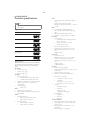
TABLE OF CONTENTS
Page
. Location of PCB BdsÿVersion Variation and Repair Scenario Matrix..........1-2
. Technical Specifications…………....………………………..............1-3
. Safety Instruction, Warning & Notes….……………………....….....1-4
. DFU Instruction..............................................................................2-1
. Mechanical and Dismantling Instructions…………........................3-1
. Software Upgrades and Region Code Change..............................4-1
. Trouble Shooting Chart………………………………………………. 5-1
. Wiring Diagram………………………………………..………..….….6-1
. Electrical Diagrams and Print-layouts..….…………………....….…7-1
. Set Mechanical Exploded view & Part list.…………………..….….8-1
. Revision List..................................................................................9-1
©Copyright 2010 Philips Consumer Electronics B.V. Eindhoven, The Netherlands
All rights reserved. No part of this publication may be reproduced, stored in aretrieval system or
transmitted, in any form or by any means, electronic, mechanical, photocopying, or otherwise
without the prior permission of Philips.
Published by RY - 039 BU AVM
Version 1.2
Printed in The Netherlands
Subject to modification
CLASS 1
LASER PRODUCT
GB
3139 785 35222
PHILIPS
1-2
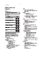
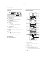
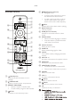
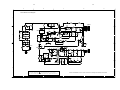
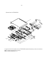
LOCATION OF PCB BOARDS:
AM PCB
MAIN PCB
POWER PCB
LOADER
FRONT
CONTROL PCB
Version Variation:
Type/Versions
Features
Output Power-600W
HTS3520
/05
/12
/51
X
X
X
Output Power-480W
Voltage(220~240v)
X
/55
/x78
/94
/98
X
X
X
X
X
X
X
X
X
Voltage(110~240v)
Voltage(220~230v)
X
Repair Scenario Matrix:
Type/Versions
HTS3520
/05
/12
/51
/55
/x78
/94
/98
Main Board
C
C
C
C
C
C
C
Front Control Board
C
C
C
C
C
C
C
Amplifier Board
C
C
C
C
C
C
C
Power Board
C
C
C
C
C
C
C
Board in used
*Bd:Board Level Replacement
*C:Component Level Repair
1-3
HTS3520/12/05:
Product specifications
Note
• Specification and design are subject to change
without notice.
Region code
Country
DVD
Europe, United Kingdom
Asia Pacific, Taiwan, Korea
Latin America
Australia, New Zealand
Russia, India
China
Playback media
DVD-Video, DVD+R/+RW, DVD-R/-RW, DVD+R
DL, CD-R/CD-RW, Audio CD, Video CD/SVCD,
Picture CD, MP3-CD, WMA-CD, USB storage
device
File Format
•
Audio: .mp3, .wma
•
Video: .mpeg, .mpg,
•
Picture: .jpeg, .jpg
Amplifier
•
Total output power:
• HTS3510: 300 W RMS
• HTS3520: 600 W RMS
•
Frequency response: 20 Hz-20 kHz / ±3dB
•
Signal-to-noise ratio: > 65 dB (CCIR) /
(A-weighted)
•
Input sensitivity:
• AUX: 1 mV
Video
•
Signal system: PAL / NTSC
•
HDMI output: 480i/576i, 480p/576p, 720p,
1080i, 1080p
Audio
•
Sampling frequency:
• MP3: 32 kHz, 44.1 kHz, 48 kHz
• WMA: 44.1 kHz, 48 kHz
•
Constant bit rate:
• MP3: 112 kbps - 320 kbps
• WMA: 48 kbps - 192 kbps
Radio
•
Tuning range: FM 87.5-108 MHz (50 kHz)
•
Signal-to-noise ratio: FM 50 dB
•
Frequency response: FM 180 Hz-10 kHz /
±6dB
USB
•
Compatibility: Hi-Speed USB (2.0)
•
Class support: UMS (USB Mass Storage
Class)
•
File system: FAT12, FAT16, FAT32
•
Maximum memory support: < 160GB.
Main Unit
•
Power supply: 220-240V; ~50 Hz
•
Power consumption: 100 W
•
Standby power consumption: < 0.9 W
•
Dimensions (WxHxD): 360 x 58 x 320
(mm)
•
Weight: 2.84 kg
Subwoofer
•
Impedance: 8 ohm
•
Speaker drivers: 165 mm (6.5”) woofer
•
Frequency response: 40 Hz-150 kHz
•
Dimensions (WxHxD): 120 x 307 x 369
(mm)
•
Weight: 3.84 kg
•
Cable length: 4.3 m
Speakers
•
System: full range satellite
•
Speaker impedance: 8 ohm (center), 4 ohm
(Front/Rear)
•
Speaker drivers: 3” full range
Frequency response: 150 Hz-20 kHz
•
•
Dimensions (WxHxD):
• HTS3510: 96 x 162 x 96 (mm)
• HTS3520:
Center: 160.9 x 95 x 92 (mm)
Front/Rear: 95 x 160.9 x 87 (mm)
•
Weight:
• HTS3510: 0.68 kg
• HTS3520:
Center: 0.77 kg
Front/Rear: 0.56 kg/each
•
Cable length:
• Center: 3 m
• Front: 4 m
• Rear: 10 m
Laser specification
•
Type: Semiconductor laser GaAIAs (CD)
•
Wave length: 645 - 665 nm (DVD), 770 800 nm (CD)
•
Output power: 6 mW (DVD), 7 mW
(VCD/CD)
•
Beam divergence: 60 degrees.
1-4
HTS3520/55/X78:
Product specifications
Note
• Specification and design are subject to change
without notice.
Region code
Country
DVD
Europe, United Kingdom
Asia Pacific, Taiwan, Korea
Latin America
Australia, New Zealand
Russia, India
China
Playback media
DVD-Video, DVD+R/+RW, DVD-R/-RW, DVD+R
DL, CD-R/CD-RW, Audio CD, Video CD/SVCD,
Picture CD, MP3-CD, WMA-CD, USB storage
device
File Format
•
Audio: .mp3, .wma
•
Video: .mpeg, .mpg,
•
Picture: .jpeg, .jpg
Amplifier
•
Total output power:
• HTS3510: 240 W RMS (10% THD)
• HTS3520: 480 W RMS (10% THD)
•
Frequency response: 20 Hz-20 kHz / ±3dB
•
Signal-to-noise ratio: > 65 dB (CCIR) /
(A-weighted)
•
Input sensitivity:
• AUX: 1 mV
Video
•
Signal system: PAL / NTSC
•
HDMI output: 480i/576i, 480p/576p, 720p,
1080i, 1080p
Audio
•
Sampling frequency:
• MP3: 32 kHz, 44.1 kHz, 48 kHz
• WMA: 44.1 kHz, 48 kHz
•
Constant bit rate:
• MP3: 112 kbps - 320 kbps
• WMA: 48 kbps - 192 kbps
Radio
•
Tuning range: FM 87.5-108 MHz (50/100
kHz)
•
Signal-to-noise ratio: FM 50 dB
•
Frequency response: FM 180 Hz ~ 10 kHz
/ ±6dB
USB
•
Compatibility: Hi-Speed USB (2.0)
•
Class support: UMS (USB Mass Storage
Class)
•
File system: FAT12, FAT16, FAT32
•
Maximum memory support: < 160GB.
Main Unit
•
Power supply:
• Asia Pacific/Latin America/India: 110240V, ~50-60Hz
• China: 220-230V, ~50-60Hz
• Russia: 230V, ~50Hz
•
Power consumption: 100 W
•
Standby power consumption: < 0.9 W
•
Dimensions (WxHxD): 360 x 58 x 320
(mm)
•
Weight: 2.84 kg
Subwoofer
•
Impedance: 8 ohm
•
Speaker drivers: 165 mm (6.5”) woofer
•
Frequency response: 40 Hz-150 kHz
•
Dimensions (WxHxD): 120 x 307 x 369
(mm)
•
Weight: 3.84 kg
•
Cable length: 4.3 m
Speakers
•
System: full range satellite
•
Speaker impedance: 8 ohm (center), 4 ohm
(Front/Rear)
•
Speaker drivers: 3” full range
•
Frequency response: 150 Hz-20 kHz
•
Dimensions (WxHxD):
HTS3510: 96 x 162 x 96 (mm)
HTS3520:
Center: 160.9 x 95 x 92 (mm)
Front/Rear: 95 x 160.9 x 87 (mm)
•
Weight:
• HTS3510: 0.68 kg
• HTS3520:
Center: 0.77 kg
Front/Rear: 0.56 kg/each
•
Cable length:
• Center: 3 m
• Front: 4 m
• Rear: 10 m
Laser specification
•
Type: Semiconductor laser GaAIAs (CD)
•
Wave length: 645 - 665 nm (DVD), 770 800 nm (CD)
•
Output power: 6 mW (DVD), 7 mW
(VCD/CD)
•
Beam divergence: 60 degrees.
•
•
1-5
HTS3520/51:
1-6
1-7
HTS3520/94:
1-8
Speakers
•
System: full range satellite
•
Speaker impedance: 8 ohm (center), 4 ohm
(Front/Rear)
•
Speaker drivers: 3” full range
•
Frequency response: 150 Hz-20 kHz
•
Dimensions (WxHxD):
• HTS3510: 96 x 162 x 96 (mm)
• HTS3520:
Center: 160.9 x 95 x 92 (mm)
Front/Rear: 95 x 160.9 x 87 (mm)
•
Weight:
• HTS3510: 0.68 kg
• HTS3520:
Center: 0.77 kg
Front/Rear: 0.56 kg/each
•
Cable length:
• Center: 3 m
• Front: 4 m
• Rear: 10 m
Laser specification
•
Type: Semiconductor laser GaAIAs (CD)
•
Wave length: 645 - 665 nm (DVD), 770 800 nm (CD)
•
Output power: 6 mW (DVD), 7 mW
(VCD/CD)
•
Beam divergence: 60 degrees.
1-9
HTS3520/98:
Product Specification
1-10
1-11
Safety instruction, Warning & Notes
Safety instruction
1. General safety
2.Laser safety
Safety regulations require that during a repair:
. Connect the unit to the mains via an isolation transformer.
. Replace safety components indicated by the symbol
,
only by components identical to the original ones. Any
other component substitution (other than original type)
may increase risk of fire or electrical shock hazard.
This unit employs a laser. Only qualified service personnel
may remove the cover, or attempt to service this device
(due to possible eye injury).
Laser device unit
Type
: Semiconductor laser GaAlAs
Wavelength
: 650nm (DVD)
: 780nm (VCD/CD)
Safety regulations require that after a repair, you must
return the unit in its original condition. Pay, in particular,
Output power
: 10mW (DVD /CD)
attention to the following points:
. Route the wires/cables correctly, and fix them with the
. Check the insulation of the mains lead for external
procedure other than those specified herein, may result in
hazardous radiation exposure. Avoid direct exposure to
damage.
. Check the electrical DC resistance between the mains
plug and the secondary side:
1) Unplug the mains cord, and connect a wire between
the two pins of the mains plug.
2) Set the mains switch the “on” position (keep the
mains cord unplug).
3) Measure the resistance value between the mains
plug and the front panel, controls, and chassis
bottom.
Repair
Beam divergence: 60 degree
Note: Use of controls or adjustments or performance of
mounted cable clamps.
4)
: 7mW (DVD)
or
correct
unit
when
¡
measurement is less than 1M .
the
resistance
5) Verify this, before you return the unit to the
customer/user (ref. UL-standard no. 1492).
6) Switch the unit “off”, and remove the wire between
the two pins of the mains plug.
beam.
1-12
Warning
1.General
2. Laser
. All ICs and many other semiconductors are susceptible to
. The use of optical instruments with this product, will
electrostatic discharges (ESD). Careless handing during
increase eye hazard.
repair can reduce life drastically. Make sure that, during
. Only qualified service personnel may remove the cover
repair, you are at the same potential as the mass of the
or attempt to service this device, due to possible eye
set by a wristband with resistance. Keep components and
injury.
tools at this same potential. Available ESD protection
with a disc loaded inside the player.
equipment:
1)
. Repair handing should take place as much as possible
Complete kit ESD3 (small tablemat, wristband,
connection box, extension cable and earth cable)
. Text below is placed inside the unit, on the laser cover
shield:
4822 310 10671.
2)
Wristband tester 4822 344 13999.
. Be careful during measurements in the live voltage
section. The primary side of the power supply , including
the heat sink, carries live mains voltage when you
CAUTION: VISIBLE AND INVISIBLE LASER
RADIATION WHEN OPEN, AVOID EXPOSURE
TO BEAM.
connect the player to the mains (even when the player is
“off”!). It is possible to touch copper tracks and/or
components in this unshielded primary area, when you
Notes:
service
Laboratories. The double-D symbol is trademarks of Dolby
the
player.
Service
personnel
must
take
precautions to prevent touching this area or components
in this area. A “lighting stroke” and a stripe-marked
printing on the printed wiring board, indicate the primary
side of the power supply.
. Never replace modules, or components, while the unit is
“on”.
Manufactured
under
licence
Laboratories, Inc. All rights reserved.
from
Dolby
1-13
6HUYLFH+LQWV
&$87,21
&+$5*('&$3$&,7256217+(6(592%2$5'0$<'$0$*(7+('5,9(
(/(&7521,&6:+(1&211(&7,1*$1(:'5,9(7+$7¶6:+<%(6,'(67+(6$)(7<
0($685(6/,.(
6:,7&+2))32:(56833/<
(6'3527(&7,21
$'',7,21$/$&7,2160867%(7$.(1%<7+(5(3$,57(&+1,&,$1
7KHIROORZLQJVWHSVKDYHWREHGRQHZKHQUHSODFLQJWKHGHIHFWLYHORDGHU
'LVPDQWOLQJRIWKHORDGHUWRDFFHVVWKH(6'SURWHFWLRQSRLQWLIQHFHVVDU\
6ROGHUWKH(6'SURWHFWLRQSRLQW 'LVFRQQHFWÀH[IRLOFDEOHIURPWKHGHIHFWLYHORDGHU
3XWDSDSHUFOLSRQWKHÀH[IRLOWRVKRUWFLUFXLWWKHFRQWDFWV¿J
5HSODFHWKHGHIHFWLYHORDGHUZLWKDQHZORDGHU
5HPRYHSDSHUFOLSIURPWKHÀH[IRLODQGFRQQHFWLWWRWKHQHZORDGHU
5HPRYHVROGHUMRLQWRQWKH(6'SURWHFWLRQSRLQW
$77(17,217KHODVHUGLRGHRIWKLVORDGHULVSURWHFWHGDJDLQVW(6'E\DVROGHUMRLQWZKLFKVKRUWFLUFXLWVWKHODVHUGLRGHWRJURXQG
)RUSURSHUIXQFWLRQDOLW\RIWKHORDGHUWKLVVROGHUMRLQWPXVWEHUHPRYHDIWHUFRQQHFWLRQORDGHUWRWKHVHW
Solder Joint
(6'SURWHFWLRQSRLQWLVDFFHVVLEOHIURPWRSRIORDGHU
2QO\DSSOLFDEOHIRUGHIHFWLYHORDGHUQHHGHGWREHVHQWEDFNWRVXSSOLHUIRUIDLOXUHDQDO\VLVDQGWRVXSSRUWEDFNFKDUJLQJ
HYLGHQFH
7KLVLVDOVRDSSOLFDEOHIRUDOOSDUWQHUVKLSZRUNVKRSV
1-14
Notes
Lead-Free requirement for service
INDENTIFICATION:
x
Regardless of special logo (not always indicated)
Use only original spare-parts listed in the
Service-Manuals. Not listed standard-material
(commodities) has to be purchased at external
One must treat all sets from 1.1.2005 onwards, according
next rules.
companies.
x
Important note: In fact also products a little older can also
be treated in this way as long as you avoid mixing
solder-alloys (leaded/ lead-free). So best to always use
SAC305 and the higher temperatures belong to this.
Special information for BGA-ICs:
- always use the 12nc-recognizable soldering
temperature profile of the specific BGA (for
de-soldering
always
use
highest
lead-free
temperature profile, in case of doubt)
Due to lead-free technology some rules have to be
respected by the workshop during a repair:
- lead free BGA-ICs will be delivered in so-called
x Use only lead-free solder alloy Philips SAC305 with
‘dry-packaging’ (sealed pack including a silica gel
order code 0622 149 00106. If lead-free solder-paste is
pack) to protect the IC against moisture. After
required, please contact the manufacturer of your
opening, dependent of MSL-level seen on
solder-equipment. In general use of solder-paste within
indicator-label in the bag, the BGA-IC possibly
workshops should be avoided because paste is not easy
still
to store and to handle.
communicated via AYS-website.
to
be
baked
dry.
This
will
be
Do not re-use BGAs at all.
x Use only adequate solder tools applicable for lead-free
solder alloy. The solder tool must be able
has
x
For sets produced before 1.1.2005, containing
o To reach at least a solder-temperature of 400°C,
leaded soldering-tin and components, all needed
o To stabilize the adjusted temperature at the
spare-parts will be available till the end of the
solder-tip
o To exchange solder-tips for different applications.
x Adjust your solder tool so that a temperature around
360°C – 380°C is reached and stabilized at the solder
joint. Heating-time of the solder-joint should not exceed
service-period. For repair of such sets nothing
changes.
x On our website:
www.atyourservice.ce.Philips.com
You find more information to:
~ 4 sec. Avoid temperatures above 400°C otherwise
BGA-de-/soldering (+ baking instructions)
wear-out of tips will rise drastically and flux-fluid will be
Heating-profiles of BGAs and other ICs used in
destroyed. To avoid wear-out of tips switch off un-used
Philips-sets
equipment, or reduce heat.
x Mix of lead-free solder alloy / parts with leaded solder
alloy / parts is possible but PHILIPS recommends
You will find this and more technical information
within the “magazine”, chapter “workshop news”.
strongly to avoid mixed
For additional questions please contact your local
solder alloy types (leaded and lead-free). If one cannot
repair-helpdesk.
avoid, clean carefully the
solder-joint from old solder alloy and re-solder with new
solder alloy (SAC305).
2-1
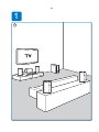
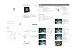
QSG for HTS3520/12/05/55/51/X78/94/98
The following excerpt of the Quick Start Guide serves as an introduction to the set.
The complete Direction For Use can be download in different languages from
Philips Customer Contact & Support site: www.p4c.philips.com
User Manual
HDMI
Audio/Video
FM
HDMI Cable for /55/X78, and Power socket transition for /55.
* Adaptador fornecido como acessório não deverá ser usado nas redes elétricas do Brasil, seu uso é destinado exclusivamente a
outros países da América Latina.
2-2
1
1
2-3
2
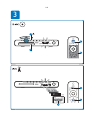
FRONT
RIGHT
FRONT
LEFT
FRONT
CENTER
SUBWOOFER
REAR
RIGHT
3
REAR
LEFT
FM
Cable
2-4
4
HDMI
Cable
Audio
Cable
5
1
6
2
AAA
x2
2-5
2
HDMI
1
USB
Settings
TV
General Setup
2
3
General Setup
5
6
Disc Lock
Auto
Display Dim
English
OSD Language
Español
Screen Saver
Português
Sleep Timer
DivX(R) VOD Code
2-6
3
1
3
2
4
1
2
3
2-7
2
1
3
User Manual
www.philips.com/support
Specifications are subject to change without notice
Trademarks are the property of Koninklijke Philips Electronics N.V.
or their respective owners
2010 © Koninklijke Philips Electronics N.V. All rights reserved.
sgythy_1001/55/v1
2-8
HTS3520/12/05:
Main unit
Remote control
a
b
a Disc compartment
b
(Open/Close)
Opens or closes the disc compartment.
c
(Play/Pause)
Starts, pauses or resumes play.
d
•
•
e
(Stop)
Stops play.
In radio mode, erases the current
preset radio station.
(Standby-On)
Switches the home theater on or to
standby.
f SOURCE
Selects an audio/video source for the home
theater.
g
v
d
u
e
t
•
Skips to the previous or next track,
chapter or file.
In radio mode, selects a preset radio
station.
h Display panel
i Volume control wheel
f
g
s
h
r
q
/
•
c
i
j
p
o
k
n
m
l
a
(Standby-On)
Switches the home theater on or to
standby.
b
OPEN/CLOSE
Opens or closes the disc compartment.
c SLEEP
Switches the home theater to standby after
the preset time selected.
d
SETUP
Accesses or exits the setup menu.
2-9
e
•
•
•
f
(Navigation buttons)
Navigate menus.
In video mode, press left or right to
fast backward or fast forward.
In radio mode, press left or right to
search a radio station; press up or
down to fine tune a radio frequency.
INFO
Displays information about what is playing.
g Playback buttons
Control playback.
h SURR (Surround Sound)
Switches to surround sound or stereo
sound.
i AUDIO SYNC
• Selects an audio language or channel.
• Press and hold to synchronize audio
with video. Use with +/-.
j Numeric buttons
Selects an item to play.
k SUBTITLE
Selects subtitle language for video.
l
SCREEN FIT
Fits the picture format to the TV screen.
m CREATE MP3/ZOOM
• Accesses the menu to create MP3.
• Zooms into a video scene or picture.
n REPEAT A-B
Marks two points within a chapter or track
for repeat play, or turns off repeat mode.
o REPEAT / PROGRAM
• Selects a repeat or shuffle mode.
• In radio mode, programs radio stations.
p ANGLE
Displays options for different camera angles.
q SOUND
Selects a sound mode.
r VOL +/Increases or decreases volume.
s
(Mute)
Mutes or restores volume.
t
BACK
Returns to a previous menu screen.
u OK
Confirms an entry or selection.
v Source buttons
• AUDIO SOURCE : Selects an audio
•
•
•
input source.
RADIO: Switches to FM radio.
USB : Switches to USB storage device.
DISC: Switches to disc source.
2-10
HTS3520/55/X78:
Main unit
Remote control
a
b
u
a Disc compartment
b
(Open/Close)
Opens or closes the disc compartment.
c
(Play/Pause)
Starts, pauses or resumes play.
d
•
•
e
d
t
e
(Stop)
Stops play.
In radio mode, erases the current
preset radio station.
s
r
(Standby-On)
Switches the home theater on or to
standby.
q
Selects an audio/video source for the home
theater.
p
/
•
•
f
g
h
f SOURCE
g
c
i
j
Skips to the previous or next track,
chapter or file.
In radio mode, selects a preset radio
station.
h Display panel
o
k
n
l
m
i Volume control wheel
a
(Standby-On)
Switches the home theater on or to
standby.
b
OPEN/CLOSE
Opens or closes the disc compartment.
c REPEAT / PROGRAM
• Selects a repeat or shuffle mode.
• In radio mode, programs radio stations.
d
SETUP
Accesses or exits the setup menu.
2-11
e
f
(Navigation buttons)
•
•
Navigate menus.
•
In radio mode, press left or right to
search a radio station; press up or down
to fine tune a radio frequency.
In video mode, press left or right to fast
backward or fast forward.
INFO
Displays information about what is playing.
g Playback buttons
Control playback.
h SURR (Surround Sound)
Switches to surround sound or stereo sound.
i AUDIO SYNC
• Selects an audio language or channel.
• Press and hold to synchronize audio
with video. Use with +/-.
j Numeric buttons
Selects an item to play.
k SUBTITLE
Selects subtitle language for video.
l VOCAL
Turns off the vocal by changing the audio channel.
m MIC VOL +/Increases or decreases microphone volume.
n KARAOKE
Accesses or exits the karaoke menu.
o CREATE MP3 / ZOOM
• Accesses the menu to create MP3.
• Zooms into a video scene or picture.
p SOUND
Selects a sound mode.
q VOL +/Increases or decreases volume.
r
(Mute)
Mutes or restores volume.
s
BACK
Returns to a previous menu screen.
t OK
Confirms an entry or selection.
u Source buttons
• AUDIO SOURCE: Selects an audio input
source.
•
•
•
RADIO: Switches to FM radio.
USB: Switches to USB storage device.
DISC: Switches to disc source.
2-12
HTS3520/51:
ǑǻǹǭȅǺǵǶ ǷǵǺǻǿDzǭǿǽ
ǜȀǸȉǿ DZǵǾǿǭǺȃǵǻǺǺǻǰǻ
ȀǼǽǭǯǸDzǺǵȌ
ǜǻǴDZǽǭǯǸȌDzǹ Ǿ ǼǻǷȀǼǷǻǶ ǵ ǼǽǵǯDzǿǾǿǯȀDzǹ
ǯǭǾ ǯ ǷǸȀǮDz Philips! ǤǿǻǮȈ ǯǻǾǼǻǸȉǴǻǯǭǿȉǾȌ
ǯǾDzǹǵ ǼǽDzǵǹȀȆDzǾǿǯǭǹǵ ǼǻDZDZDzǽdzǷǵ Philips,
ǴǭǽDzǰǵǾǿǽǵǽȀǶǿDz DZǻǹǭȅǺǵǶ ǷǵǺǻǿDzǭǿǽ Ǻǭ ǯDzǮǾǭǶǿDz www.philips.com/welcome.
a
b
u
ǛǾǺǻǯǺǻDz ȀǾǿǽǻǶǾǿǯǻ
c
d
t
e
s
a ǛǿDZDzǸDzǺǵDz DZǸȌ DZǵǾǷǭ
b
(ǛǿǷǽȈǿȉ/ǔǭǷǽȈǿȉ)
ǛǿǷǽȈǯǭDzǿ ǵǸǵ ǴǭǷǽȈǯǭDzǿ DZǵǾǷǻǯǻDZ.
r
c
(ǏǻǾǼǽǻǵǴǯDzDZDzǺǵDz / ǜǭȀǴǭ)
ǔǭǼȀǾǷ, ǼǽǵǻǾǿǭǺǻǯǸDzǺǵDz ǵǸǵ
ǯǻǴǻǮǺǻǯǸDzǺǵDz ǯǻǾǼǽǻǵǴǯDzDZDzǺǵȌ.
q
d
•
•
e
f
g
h
p
(ǞǿǻǼ)
ǛǾǿǭǺǻǯǷǭ ǯǻǾǼǽǻǵǴǯDzDZDzǺǵȌ.
Ǐ ǽDzdzǵǹDz ǽǭDZǵǻ ȀDZǭǸȌDzǿ
ǼǽDzDZȀǾǿǭǺǻǯǸDzǺǺȀȋ ǽǭDZǵǻǾǿǭǺȃǵȋ.
i
j
(ǝDzdzǵǹǭ ǻdzǵDZǭǺǵȌ ǯǷǸȋȄDzǺ)
ǏǷǸȋȄDzǺǵDz DZǻǹǭȅǺDzǰǻ ǷǵǺǻǿDzǭǿǽǭ ǵǸǵ
ǼDzǽDzǷǸȋȄDzǺǵDz ǯ ǽDzdzǵǹ ǻdzǵDZǭǺǵȌ.
o
k
n
l
m
f SOURCE
ǏȈǮDzǽǵǿDz DZǸȌ DZǻǹǭȅǺDzǰǻ ǷǵǺǻǿDzǭǿǽǭ
ǵǾǿǻȄǺǵǷ ǭȀDZǵǻ- ǵ ǯǵDZDzǻǾǵǰǺǭǸǭ.
g
/
•
•
ǜDzǽDzȂǻDZ Ƿ ǼǽDzDZȈDZȀȆDzǶ ǵǸǵ
ǾǸDzDZȀȋȆDzǶ DZǻǽǻdzǷDz, ǽǭǴDZDzǸȀ ǵǸǵ
ȁǭǶǸȀ.
Ǐ ǽDzdzǵǹDz ǽǭDZǵǻ: ǯȈǮǻǽ
ǾǻȂǽǭǺDzǺǺǻǶ ǽǭDZǵǻǾǿǭǺȃǵǵ.
h ǑǵǾǼǸDzǶ
i ǝDzǰȀǸȌǿǻǽ ǰǽǻǹǷǻǾǿǵ
a
(ǝDzdzǵǹǭ ǻdzǵDZǭǺǵȌ ǯǷǸȋȄDzǺ)
ǏǷǸȋȄDzǺǵDz DZǻǹǭȅǺDzǰǻ ǷǵǺǻǿDzǭǿǽǭ ǵǸǵ
ǼDzǽDzǷǸȋȄDzǺǵDz ǯ ǽDzdzǵǹ ǻdzǵDZǭǺǵȌ.
b
OPEN/CLOSE
ǛǿǷǽȈǯǭDzǿ ǵǸǵ ǴǭǷǽȈǯǭDzǿ DZǵǾǷǻǯǻDZ.
2-13
c REPEAT / PROGRAM
• ǏȈǮǻǽ ǽDzdzǵǹǭ ǼǻǯǿǻǽǺǻǰǻ
•
d
SETUP
ǏȂǻDZ ǵ ǯȈȂǻDZ ǵǴ ǹDzǺȋ ǺǭǾǿǽǻDzǷ.
e
•
•
•
f
ǯǻǾǼǽǻǵǴǯDzDZDzǺǵȌ ǵǸǵ
ǯǻǾǼǽǻǵǴǯDzDZDzǺǵȌ ǯ ǼǽǻǵǴǯǻǸȉǺǻǹ
ǼǻǽȌDZǷDz.
Ǐ ǽDzdzǵǹDz ǽǭDZǵǻ: ǼǽǻǰǽǭǹǹǵǽǻǯǭǺǵDz
ǽǭDZǵǻǾǿǭǺȃǵǶ.
(ǗǺǻǼǷǵ ǼDzǽDzǹDzȆDzǺǵȌ)
ǜDzǽDzǹDzȆDzǺǵDz Ǽǻ ǹDzǺȋ.
Ǐ ǽDzdzǵǹDz ǯǵDZDzǻ: ǷǺǻǼǷǵ “ǯǼǽǭǯǻ” ǵ
“ǯǸDzǯǻ” ǵǾǼǻǸȉǴȀȋǿǾȌ DZǸȌ ǮȈǾǿǽǻǰǻ
ǼDzǽDzȂǻDZǭ ǺǭǴǭDZ ǵǸǵ ǯǼDzǽDzDZ.
Ǐ ǽDzdzǵǹDz ǽǭDZǵǻ: ǷǺǻǼǷǵ “ǯǼǽǭǯǻ”
ǵ “ǯǸDzǯǻ” ǵǾǼǻǸȉǴȀȋǿǾȌ DZǸȌ
ǼǻǵǾǷǭ ǽǭDZǵǻǾǿǭǺȃǵǵ; DZǸȌ
ǿǻȄǺǻǶ ǺǭǾǿǽǻǶǷǵ ǽǭDZǵǻȄǭǾǿǻǿȈ
ǵǾǼǻǸȉǴȀȋǿǾȌ ǷǺǻǼǷǵ “ǯǯDzǽȂ” ǵ
“ǯǺǵǴ”.
INFO
ǛǿǻǮǽǭdzDzǺǵDz ǵǺȁǻǽǹǭȃǵǵ ǻ
ǯǻǾǼǽǻǵǴǯǻDZǵǹȈȂ ǹǭǿDzǽǵǭǸǭȂ.
g ǗǺǻǼǷǵ ȀǼǽǭǯǸDzǺǵȌ ǯǻǾǼǽǻǵǴǯDzDZDzǺǵDzǹ
ǠǼǽǭǯǸDzǺǵDz ǯǻǾǼǽǻǵǴǯDzDZDzǺǵDzǹ.
h SURR (ǛǮȇDzǹǺȈǶ ǴǯȀǷ)
ǜDzǽDzǷǸȋȄDzǺǵDz ǹDzdzDZȀ ǽDzdzǵǹǭǹǵ
ǻǮȇDzǹǺǻǰǻ ǵǸǵ ǾǿDzǽDzǻǴǯȀǷǭ.
i AUDIO SYNC
• ǏȈǮǻǽ ȌǴȈǷǭ ǭȀDZǵǻǾǻǼǽǻǯǻdzDZDzǺǵȌ
•
ǵǸǵ ǷǭǺǭǸǭ.
ǚǭdzǹǵǿDz ǵ ȀDZDzǽdzǵǯǭǶǿDz ȊǿȀ ǷǺǻǼǷȀ,
ȄǿǻǮȈ ǾǵǺȂǽǻǺǵǴǵǽǻǯǭǿȉ ǭȀDZǵǻ ǵ
ǯǵDZDzǻ. ǕǾǼǻǸȉǴȀǶǿDz ǷǺǻǼǷǵ +/-.
j Numeric buttons
ǏȈǮǻǽ ȊǸDzǹDzǺǿǭ DZǸȌ ǯǻǾǼǽǻǵǴǯDzDZDzǺǵȌ.
k SUBTITLE
ǏȈǮǻǽ ȌǴȈǷǭ ǾȀǮǿǵǿǽǻǯ DZǸȌ ǯǵDZDzǻ.
l VOCAL
ǛǿǷǸȋȄDzǺǵDz ǯǻǷǭǸǭ ǼǻǾǽDzDZǾǿǯǻǹ
ǵǴǹDzǺDzǺǵȌ ǭȀDZǵǻǷǭǺǭǸǭ.
m MIC VOL +/ǠǯDzǸǵȄDzǺǵDz ǵǸǵ ȀǹDzǺȉȅDzǺǵDz ǰǽǻǹǷǻǾǿǵ
ǹǵǷǽǻȁǻǺǭ.
n KARAOKE
ǑǻǾǿȀǼ ǵǸǵ ǯȈȂǻDZ ǵǴ ǹDzǺȋ ǷǭǽǭǻǷDz.
o CREATE MP3 / ZOOM
• ǑǻǾǿȀǼ Ƿ ǹDzǺȋ DZǸȌ ǾǻǴDZǭǺǵȌ MP3•
ȁǭǶǸǻǯ.
ǠǯDzǸǵȄDzǺǵDz ǹǭǾȅǿǭǮǭ ǯǵDZDzǻȊǼǵǴǻDZǭ
ǵǸǵ ǵǴǻǮǽǭdzDzǺǵȌ.
p SOUND
ǏȈǮǻǽ ǽDzdzǵǹǭ ǴǯȀǷǭ.
q VOL +/ǝDzǰȀǸǵǽǻǯǷǭ ǰǽǻǹǷǻǾǿǵ.
r
(ǎDzǴ ǴǯȀǷǭ)
ǛǿǷǸȋȄDzǺǵDz ǵǸǵ ǯǻǾǾǿǭǺǻǯǸDzǺǵDz ǴǯȀǷǭ.
s
BACK
ǏǻǴǯǽǭǿ Ƿ ǼǽDzDZȈDZȀȆDzǹȀ ȊǷǽǭǺȀ ǹDzǺȋ.
t OK
ǜǻDZǿǯDzǽdzDZDzǺǵDz ǯǯǻDZǭ ǵǸǵ ǯȈǮǻǽǭ.
u ǗǺǻǼǷǵ Source
• AUDIO SOURCE : ǏȈǮǻǽ ǵǾǿǻȄǺǵǷǭ
•
•
•
ǭȀDZǵǻǯȂǻDZǭ.
RADIO: ǜDzǽDzǷǸȋȄDzǺǵDz ǯ ǽDzdzǵǹ
FM-ǽǭDZǵǻ.
USB : ǜDzǽDzǷǸȋȄDzǺǵDz ǯ ǽDzdzǵǹ
ǴǭǼǻǹǵǺǭȋȆDzǰǻ USB-ȀǾǿǽǻǶǾǿǯǭ.
DISC: ǜDzǽDzȂǻDZ Ƿ DZǵǾǷȀ.
2-14
HTS3520/94:
Your home theater
Congratulations on your purchase, and welcome
to Philips! To fully benefit from the support that
Philips offers, register your home theater at www.
philips.com/welcome.
Main unit
a Disc compartment
b
(Open/Close)
Opens or closes the disc compartment.
c
(Play/Pause)
Starts, pauses or resumes play.
d
•
•
e
(Stop)
Stops play.
In radio mode, erases the current
preset radio station.
(Standby-On)
Switches the home theater on or to
standby.
f SOURCE
Selects an audio/video source for the home
theater.
g
/
•
•
Skips to the previous or next track,
chapter or file.
In radio mode, selects a preset radio
station.
h Display panel
i Volume control wheel
2-15
e
Remote control
•
•
a
•
b
u
c
d
t
s
r
p
INFO
Displays information about what is playing.
g Playback buttons
Control playback.
e
h SURR (Surround Sound)
f
i AUDIO SYNC
• Selects an audio language or channel.
• Press and hold to synchronize audio
Switches to surround sound or stereo
sound.
g
h
q
f
(Navigation buttons)
Navigate menus.
In video mode, press left or right to
fast backward or fast forward.
In radio mode, press left or right to
search a radio station; press up or
down to fine tune a radio frequency.
i
with video. Use with +/-.
j Numeric buttons
Selects an item to play.
k SUBTITLE
Selects subtitle language for video.
l VOCAL
Turns off the vocal by changing the audio
channel.
j
m MIC VOL +/-
o
k
n
l
m
Increases or decreases microphone volume.
n KARAOKE
Accesses or exits the karaoke menu.
o CREATE MP3 / ZOOM
• Accesses the menu to create MP3.
• Zooms into a video scene or picture.
p SOUND
Selects a sound mode.
a
b
(Standby-On)
Switches the home theater on or to
standby.
OPEN/CLOSE
Opens or closes the disc compartment.
c REPEAT / PROGRAM
• Selects a repeat or shuffle mode.
• In radio mode, programs radio stations.
d
SETUP
Accesses or exits the setup menu.
q VOL +/Increases or decreases volume.
r
(Mute)
Mutes or restores volume.
s
BACK
Returns to a previous menu screen.
t OK
Confirms an entry or selection.
2-16
HTS3520/98:
Your home theater
Congratulations on your purchase, and welcome
to Philips! To fully benefit from the support that
Philips offers, register your home theater at www.
philips.com/welcome.
Main unit
a Disc compartment
b
(Open/Close)
Opens or closes the disc compartment.
c
(Play/Pause)
Starts, pauses or resumes play.
d
•
•
e
(Stop)
Stops play.
In radio mode, erases the current
preset radio station.
(Standby-On)
Switches the home theater on or to
standby.
f SOURCE
Selects an audio/video source for the home
theater.
g
/
•
•
Skips to the previous or next track,
chapter or file.
In radio mode, selects a preset radio
station.
h Display panel
i Volume control wheel
2-17
e
Remote control
•
•
a
•
b
u
c
f
d
g Playback buttons
INFO
Displays information about what is playing.
Control playback.
t
e
s
(Navigation buttons)
Navigate menus.
In video mode, press left or right to
fast backward or fast forward.
In radio mode, press left or right to
search a radio station; press up or
down to fine tune a radio frequency.
f
h SURR (Surround Sound)
Switches to surround sound or stereo sound.
i AUDIO SYNC
• Selects an audio language or channel.
• Press and hold to synchronize audio
with video. Use with +/-.
r
g
Selects an item to play.
h
q
p
j Numeric buttons
k SUBTITLE
Selects subtitle language for video.
i
l VOCAL
Turns off the vocal by changing the audio channel.
j
m MIC VOL +/Increases or decreases microphone volume.
n KARAOKE
o
k
n
l
m
Accesses or exits the karaoke menu.
o CREATE MP3 / ZOOM
• Accesses the menu to create MP3.
• Zooms into a video scene or picture.
p SOUND
Selects a sound mode.
q VOL +/Increases or decreases volume.
a
b
(Standby-On)
Switches the home theater on or to
standby.
OPEN/CLOSE
Opens or closes the disc compartment.
c REPEAT / PROGRAM
• Selects a repeat or shuffle mode.
• In radio mode, programs radio stations.
d
SETUP
Accesses or exits the setup menu.
r
(Mute)
Mutes or restores volume.
s
BACK
Returns to a previous menu screen.
t OK
Confirms an entry or selection.
u Source buttons
• AUDIO SOURCE : Selects an audio
•
•
•
input source.
RADIO: Switches to FM radio.
USB : Switches to USB storage device.
DISC: Switches to disc source.
3-1
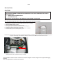
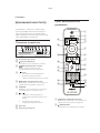
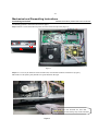
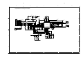
Mechanical and Dismantling Instructions
Dismantling Instruction
Detailed information please refer to the model set.
The following guidelines show how to dismantle the player.
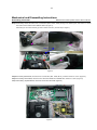
Step1: Remove 6 screws around the Top Cover, and then remove the Top Cover (Figure 1).
Figure 1
Step2: If it is necessary to dismantle Loader or Front Panel, the Front door should be removed first. (Figure 2)
Note: Make sure to operate gently otherwise the guider would be damaged.
Please kindly note that dismantle the front door
assembly carefully to avoid damage tray and the front door.
Figure 2
3-2
Mechanical and Dismantling Instructions
Detailed information please refer to the model set.
Dismantling Instruction
Step3: If the tray can’t open in normal way, you can make it through the instruction as below (Figure 3).
Note: Make sure to operate gently otherwise the guider would be damaged.
Figure 3
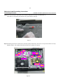
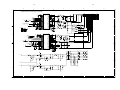
Step4: Dismantling Front Panel, disconnect the connectors (XP16, XP20, XP9), need release 2 snaps of Front Panel & 2 snaps
of bottom cabinet , then gently pull the Panel out from the set. (Figure 4 - Figure 6)
XP16
XP12
XP10
XP13
XP11 XS703
XP14
XP1
CON501
XP20 XP9
Bottom snap
Side snap
Figure 4
3-3
Mechanical and Dismantling Instructions
Dismantling Instruction
Detailed information please refer to the model set.
Step5: Dismantling Loader, disconnect the 3 connectors (XP12, XP13, XP14) aiming in the below figure, and remove 2 screws
that connects the loader and the bottom cabinet. (Figure 5)
Dismantling the Turn Knob assembly, pls refer to below instruction. (The last steps of Figure 5)
Figure 5
Step6: Dismantling Main Board, first disconnect 3 connectors (XP1, XP10, XP11), and then remove 8 screws. (Figure 6)
Step7: Dismantling Power Board, disconnect the connectors XS703 and CON501 then remove 4 screws. (Figure 6)
Step8: Dismantling Amplifier Board, remove 8 screws from the PCB. (Figure 6)
Figure 6
4-1
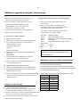
Softeware upgrade and region code change
Preparation to upgrade software
1) Power on the set and open the tray, then press "5""5"
B. Read out the software versions to confirm upgrading
on remote control to check the SW File Name.
2) Start the CD Burning software and create a new CD
1)
project (Data Disc) with the following setting:
Lable: HTSXXXX (No need the label name)
2)
SW File Name: HTSXXXX_XX.BIN
Note: It is required to keep the SW file name accord.
3) Burn the data onto a blank CDR
A.
Procedure for software upgrade:
A) Upgrade software via CDR:
1)
Power on the set and insert the prepared Upgrade CDR.
2)
The set will starts reading disc & response with the
following display TV screen:
Upgrade File DETECTED
Power on the set and press "Setup" button on the
remote control.
Press "1""3""7""9" button or press down cursor
on remote control to select "Preferences" and press
right & down cursor to select "Version Info".
The software version and other informations will be
displayed on the TV screen as follows:
File Name
HTSXXXX_XX.BIN
Version
XX.XX.XX.XX (Main version)
Sub-Ver
XX.XX.XX.XX (version of applicaton software)
RISC
XX.XX.XX.XX
Servo
XX.XX.XX.XX (software version of Servo)
Region Code
X
HDCP
PASS
MCU
XX
Upgrade?
Press Play TO START.
3)
Press "OK" button to confirm, then screen will display:
Files coping...
UPGRADING...
4)
The upgraded tray will automatically open when file
copying completed, then take the disc out.
5)
About 1 minute later, the trace will automatically close
Caution: The set must not be power off during
upgrading, Otherwise the Main board will be
damaged entirely.
Software version switch instructions
when upgrading completed.
B) Upgrade software via USB Flash Drive:
1). Power on the set and open the tray;
2). Press “6””6””6””6” and “Audio” button on the remote control;
1)
Create the correct software file onto the USB flash drive.
3). Press suited “Number code” below to switch to correct version;
2)
Power on the set and keep no disc, then insert it to the
4). Restart the Home theater player.
USB jack of the front panel.
3)
When the DVD player switchs to the USB state automatically,
pls follow the instructions on the TV screen to confrim the
upgrade operation.
Region Code Change
1) Power on the set and open the tray door;
2) Press the "Setup" button on the remote control, then the
setup interface will be displayed on the TV screen;
3) Move the down cursor on remote control to select "Preferences"
and press "1""3""8""9""3""1" on the remote control;
4) Then move the up or down cursor to select the region code.
Note: Restart after above steps.
*Note: The Number code must be matched with the part code.
Number code
Version
00
12
01
05
04
55
05
X78
06
08
09
51
98
94
5-1
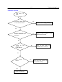
Trouble shooting Chart
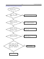
No display on VFD, and buttons do not work
No display on VFD, and
buttons do not work
Go
Check every supply
voltage on main board is
normal
No
Refer to Power supply board part
Yes
Check-24V,+3.3V,+12V
voltage on the power and
front board
No
Fix the connection XS601 on front
board and XP9 on main board
Yes
Check the power key,
open/closed key,source
key is working normaly
No
Replace U24 on main board,or replace
the main board
Yes
Check the front board
signals CS,CLK, Din/out
No
Check the U601 pin 6 7,8,9 arrive the
condition XS601 6,9,7
Yes
1.Check whether bad solder
exists on U062 and pins of VFD,
2.Check whether the circuit
connected to S603, S604, S605,
S606, S607, S608,S609 is
broken.
Yes
Replace U601 or VFD
No
Correct connection
5-2
Trouble shooting Chart
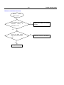
Remote control does not work
Remote
control
does not work
Go
Check whether the remote
controller’s
exhausted
battery
No
is
Replace the battery for remote
controller
or not.
Yes
Check the IR601 power
supply is OK, IR1’3 is about
3.3V
Yes
Replace IR601
No
Check the +3.3V net on front board
5-3
Trouble shooting Chart
No audio output
No audio output
Go
Check whether the +42V
Check the
No
connector XP1 pin
power is right at the
7 on main board is
XP703 on am board
3.3V
No
Yes
Yes
Refer to Power
Check
the
22pin
FFC
supply board part
connection and XS702 is
fixing OK bettew the main
board and am board
Yes
1.
Check whether the control signal is
right from the U24’15,16,33,and the
signal at the XP11’10,11,15pin
2.
Check whether the audio signal is right
from the U11'211,213,214,223,225,226, and
the signal at the XP11',2,3,4,5,8pin
Yes
Replace the am board
No
Replace U24 on main board,or
replace main board
5-4
Trouble shooting Chart
No video output
No video output
Go
Check Q23,L9,R368 is on in
main board
Yes
Check the video signal is right
from U11’187pin
No
Replace the main board
No
Add Q23,L9, R368
5-5
Trouble shooting Chart
Can’t read disc or can’t open the disk door
Can’t read disc or can’t
open the disk door
Go
Check whether the DVD
No
loader running is normal
Check the connection
6pin cable
from the main board
Yes
Check 24pin and 5pin
cable from main board
connection to the loader is
normal
Yes
Replace the loader
No
Fix the connection the 24pin and
5pincable
5-6
Trouble shooting Chart
Tuner FM does not work
Tuner FM does not work
Go
Check every supply
voltage on main board is
normal
No
Refer to Power supply board part
Yes
Check Tuner module
pin5 supply voltage is
+5V
No
Check main board tuner voltage supply
circuit.
Yes
Check Tuner module
pin7,pin8, L/R output
No
Change the Tuner module
Yes
Check the main board
U18 AK5367 PIN6,PIN7
L/R signal input
No
Check
the
main
C227,C231,R416,R421,
Yes
1:check the U18
AK5367
PIN30,VDD+5V,
1:check the U18
AK5367 Pin30, VDD+5V
Yes
Replace U18 AK5367
No
Check the main board U18
POWER SUPPLY CIRCUIT
No
Check the main board u23
(except 12/05 version)
board
5-7
Trouble shooting Chart
AUX does not work
AUX
does
not
work
Go
Check every supply voltage
on main board is normal
No
Refer to Power supply board part
Yes
Check the main board U18
AK5367 PIN4,PIN5 L/R
signal input
No
Check
the
main
C225,C230,R415,R420,
Yes
1:check the U18
AK5367
PIN30,VDD+5V,
No
Check the main board U18
POWER SUPPLY CIRCUIT
Yes
U18
ak5367
broken.
is
Yes
Replace U18 AK5367
No
Check the main board u23
(except 12/05 version)
board
6-1
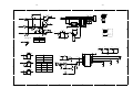
6-1
A
B
C
D
E
HTS3520 WIRING DIAGRAM
XP4
ADC
AK5367
XP3
1
DGND
+5V
DGND
+12V
4ohm 4ohm
SL-
FR-
FL-
SUB+
CE+
SR+
SL+
FR+
FL+
P201
6PIN*2.54
XP10
64M
SDRAM
10PIN*2.5
XP11
1
EEROM
16K
32M NOR
FLASH
Select use
XS303
10
T+5V/12V
GND
P_on/off
M+5V
M+5V
MGND
A+12V
GND
-27V
2
6 NORMAL POWER:
1
+32V,3A
6PIN*2.54
PEAK POWER:
+32V,6A , 1SEC
POWER
SUPPLY
1
MAX POWER:
E5V,0.5A
-35V,0.1A
A+12V,0.5A
M5V,2.5A
2
XS403
5
10
10PIN*2.5
1
LOADLOAD+
OUTSW
GND
INSW
MOTER
DRIVER
6
MTK1389S
AM5888
XP6
6PIN*2.0
24
1
SPSP+
HOMESW
GND
SLSL+
AUDIO
6 PROCESSOR+AMP
1
PGND
4PIN 2.5mm
24PIN*0.5
XP8
5PIN*2.0
(TDM-3+DOREE)
DVD LOADER
2
1
4PIN 2.5mm
MCU
48F70E
VIDEO LPF
1
4ohm
SR-
AMP
AMP
TAS5342 TAS5342
MIC
22
4ohm
CE-
+32V
EEROM
16K
4ohm
SUB-
+32V
MAIN BOARD
Pb CVBS
8ohm
+32V
P2
XP1
HDMI
Y
PGND
R
Pr
PGND
DIGITAL
AUDIO_IN
FAN
L
2PIN*2.0
SCART
22PIN
XP5
P1
1
AUDIO
PROCESSOR
TAS5808
Audio IN
9PIN*1.0
LOUT
GND
ROUT
+5V
SCLK
SDIO
/SEN
GND
/RST
GPIO2
DGND
/HP_SELO
/BKND_ERR
Shutdown signal
FAN control
AMP-DET
DGND
/POWER/RESET
MUTE
/PDN
DGND
SCL-A
SDA-A
DGND
MCLK
DGND
SCLK
LRCLK
DGND
SDIN1
SDIN2
SDIN3
22
22PIN 0.5mm
MAIN BD
FFC
1
1
12
XP2
3PIN*2.0 3
3
+5V
USB_DM
USB_DP
GND
XS302
XS301
1
14
14PIN*2.0
SWITCH XP303
BOARD 2PIN*2.0
2
2
KS62
KEY2
1
1
4 1
XP9
-27V
GND
3.3V_STB
+12V
IR
GND
DIN/OUT
CS
CLK
POW-LED-CTR
VOL+
VOLKEY1
KEY2
3
XP12
1
MIC_IN
GND
MIC_S
14PIN*2.0
1
4PIN*2.0
XS303
41
3
3PIN*2.0
XS302
2PIN*2.0
1
VFD DISPLAY+PT6315
USB MIC POT BD
4
4
Remark: Scart section only for European type and has not Karaoke output.
A
B
C
D
E
7-1
7-1
A
B
C
D
E
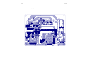
Front Board Circuit Diagram:
1
1
IR CIRCUIT
C11
0.1uF
CE6
47uF/16V
R2
R3
10K
R4
470
Q2
3DG3904M
R8
C13
2
Q5
3DG3904M
100pF
R48 100R
1
2
3
4
5
6
7
8
9
4.7K
Q3
3CG3906M
R6
R5
470
330
C16
C15
C18 C17
100pF
100pF100pF
R13
1K
+12V
GND
R34
1K
-24V
+5V
ZD2
BZX79C5V1
+
CE7
47UF 16V
C28
0.1uF
-24V
+
+5VSTANBY
R49
100
PCON
R37
10K
CE3
22uF/50V
VSTB
VCLK
VD
-24V
+12V
C24
0.1uF
C25
C26
0.1uF
0.1uF
R38
10K
R39
10K
34
35
36
37
38
39
40
41
42
43
44
G4
G3
G2
G1
VDD
LED4
LED3
LED2
LED1
GND
OSC
PT6312
U4
R44
R43
R42
2
SEG8
SEG7
SEG6/K6
SEG5/K5
SEG4/K4
SEG3/K3
SEG2/K2
SEG1/K1
VDD
KEY4
KEY3
SW1
SW2
SW3
C5
0.1uF
to power board
FB1 500ȍ
AC2
R23
51K
R35
1K
GND
AC1
-24V
100pF 100pF
JP1
5PIN/2.0mm/130mm
1 1
2 2
3 3
4 4
5 5
5.6
CE2
3.3uF/50V
R10
ZD1
10K
BZX79C6V2
R12
10K
R7
C27
0.1uF
C2
1000pF
VD
GND
PCON
POWER
OPEN
C14
R9
Q4
3DG3904M
CE1
3.3uF/50V
IR
GND
VSTB
VCLK
9PIN/2.0mm
R11
1K
AC2
33
32
31
30
29
28
27
26
25
24
23
JP2
C1
0.1uF
18K
2.2
Q1
3DG3904M
+
GND
to main board
VFD3
VFD20-0824
R1
470
+5V
G5
G6
SEG16
SEG15
SEG14
SEG13
VEE
SEG12
SEG11
SEG10
SEG9
C12
47pF
+12V
R30
100 ohm
22
21
20
19
18
17
16
15
14
13
12
K1
+5V
K2
K3
D2
FR102
SW1
SW2
SW3
SW4
SDout
SDin
GND
SCLK
/CS
KEY1
KEY2
+
REM
+5VSTANBY
1
2
3
4
5
6
7
8
9
10
11
4
2.2k
F2
F2
NP
1G
2G
3G
4G
5G
6G
7G
8G
NC
P1
P2
P3
P4
P5
P6
P7
P8
P9
P10
P11
P12
P13
NC
P14
P15
NC
NP
F1
F1
GNDVCC
GND
GND IR
3
2
1
1
2
3
4
5
6
7
8
9
10
11
12
13
14
15
16
17
18
19
20
21
22
23
24
25
26
27
28
29
30
31
32
5
+
R29
IR
IR1
R28
K2
100
100
100
2.2k
PLAY/PAUSE
C29
100pF
C30
100pF
R32
10K
C31
100pF
R27
2.2k
K3
GND
R31
3
10K
3
STOP
C22
47pF
+5VSTANBY
C32
47pF
R47
150
R36
10K
Q6
R40
3904
4.7K
OPEN
JP3
4
PICH=2.0
1
2
3
R45
LED-2
470
K1
LED-2
+5V
R33
150
OPEN/CLOSE
4
POWER
TO SWITCH BOARD
A
B
C
D
E
7-2
7-2
A
B
C
D
E
Amplifier Board Circuit Diagram: STA309A
1
1
Q702
R740
10K
1N4148
D705
5V
VD3.3V
1N4148
R739
10K
C715
EAPO
+
D701
1/2power-control
power-control
amp-det
R701
CH1A
33
R711
10K
VD3.3V
U703
FB703
FB704
FB500R
FB500R
R702
R703
33
33
FB705
FB500R
R704
33
FB706
FB707
FB500R
FB500R
R705
R706
33
33
FB708
FB709
FB710
FB500R
FB500R
FB500R
R707
R708
R709
33
33
33
R712 10K
15pF/50V C708
R777
10K
0.1uF/16V C712
VD3.3V
0.1uF/16V C710
+12V
R798
10K
15pF/50V C709
5V
15pF/50V C707
TP17
TP18
TP19
15pF/50V C706
G ND
15pF/50V C705
G ND
15pF/50V C704
4
3
2
1
15pF/50V C703
4
3
2
1
15pF/50V C702
XP702
4PIN/2.0mm
15pF/50V
C701
CON22_LINE
XP701
1
2
3
4
5
6
7
8
9
10
11
12
13
14
15
16
64
63
62
61
60
59
58
57
56
55
54
53
52
51
50
49
FB500R
FB500R
EAPO
CE701
4.7uF/16V
MOV
GND
VDD3.3
GND
NC
SDI_78
SDI_56
SDI_34
SDI_12
LRCK1
BICK1
VDD3.3
GND
NC
RESET
PLLB
IC_84P_STA309A
R713
10K
C724
0.1uF/16V
5V
3
VI
VO
2
FB500R
FB712
FB500R
+
C721
47pF/50V
C779
C720
C719
47pF/50V47pF/50V
47pF/50V
C733
47pF/50V
C732
47pF/50V
C717
0.1uF/16V
2
VD3.3V
CE721 +
22uF/16V
C718
0.1uF/16V
CH6A
CH6B
C723
47pF/50V
C725
0.1uF/16V
FB715 FB500R
R714
3.3K
1.2nF/50V
C731
CH3A
CH4A
CH5A
CH5B
C722
47pF/50V
VD3.3V
C730
0.1uF/16V
48
47
46
45
44
43
42
41
40
39
38
37
36
35
34
33
+
VD3.3V
C727
C729
1
U704
LD1117STR
OUT2A
OUT2B
NC
GND
VDD
OUT3A
OUT3B
OUT4A
OUT4B
OUT5A
OUT5B
NC
GND
VDD3.3V
OUT6A
OUT6B
+3.3V
GND
3
FB711
CH2A
PDWN
SDIO_78
SDIO_56
NC
GND
VDD
SDO_34
SDI_12
LRCKO
BICKO
NC
GND
VDD
EPAD
OUT1A
OUT1B
FB701
FB702
C714
0.1uF/16V
SA
SDA
SCL
XT1
FIL
NC
GNDA
VDDA
CKOUT
NC
GND
VDD3.3
OUT8_B
OUT8_A
OUT7_B
OUT7_A
TP5
TP6
TP7
TP8
TP9
TP10
TP11
TP12
TP13
TP14
TP15
TP16
Q701
MMBT8050C
+
C713
TP39
TP38
TP1
TP2
TP3
TP4
R710 4.7K
1N4148
17
18
19
20
21
22
23
24
25
26
27
28
29
30
31
32
2
22
21
20
19
18
17
DG ND
16
P/RESET
15
14MUTE
13
12
11SCL-A
10SDA-A
9 DG ND
8 MLCK
7DG ND
6SCLK
5LRCLK
4
3 SDIN1
2 SDIN2
1 SDIN3
VD3.3V
0.1uF/16V
22
21
20
19
18
17
16
15
14
13
12
11
10
9
8
7
6
5
4
3
2
1
C716
0.1uF/16V
0.1uF/16V
CE723
47uF/16V
CE722
MMBT8550C
22uF/16V
D704
CE703
22uF/16V
100pF/50V
C728
0.1uF/16V
+
3
C726
CE704
22uF/16V
0.1uF/16V
220pF/50V
R799
0
4
4
A
B
C
D
E
7-3
7-3
A
B
C
D
E
Amplifier Board Circuit Diagram: STA516B
U701
6
10K
R716
+
10K
0.1uF/16V
0
FB75ȍ
IN1B
VCC2A
7
29
IN1A
OUT2A
8
28
TH-WAR
OUT2A
9
27
FAULT
OUT1B
10
26
TRI-STATE
OUT1B
11
25
PWRDN
VCC1B
12
24
CONFIG
GND1B
13
23
VL
GND1A
14
VDD
VCC1A
15
21
VDD
OUT1A
16
20
GND-Reg
OUT1A
17
19
GND-CLEAN
NC
18
1uF/50V
C748
680PF/50V
C751
0.47uF/63V
C753
0.1uF/50V
R722
4K7
C764
C749
R727
10
680PF/50V
C768
0.47uF/63V
L704 22uH
1
2
0.1uF/50V
C775
0.1uF/50V
CE711
220uF/50V
CE712
220uF/50V
R729
4K7
CE713
220uF/50V
CE714
220uF/50V
CE710
1000uF/50V
+42V
+
R723
4K7
CE719
220uF/50V
CE715
220uF/50V
+39V
+
+
CE718
220uF/50V
CE716
220uF/50V
+
+42V
XS703
C752
10
1
SPK JACK
JK701
C742
0.1uF/50V
L702 22uH
1
2
L703 22uH
1
2
R719
C744
0.1uF/50V
+
IC_36P_STA516B
C737
0.1uF/50V
C743
0.47uF/63V
R721
6.2
TP32
12
11
10
9
8
7
6
5
4
3
2
1
+
22
C747
C776
0.1uF/16V
6.2
680PF/50V
C738
+
0.1uF/50V
+
R720
TP31
12
11
10
9
8
7
6
5
4
3
2
1
+
FB713
30
R718
10
TP30
SUBSUB+
SLSL+
SRSR+
C ENCEN+
TP33
FLTP34
TP35 FL+
TP36 F RTP37
FR+
R406
GND2A
1uF/50V
C736
4K7
GND2B
IN2A
0.1uF/50V
C739
C741
0.1uF/50V
4
+
TP20
TP21
TP22
TP23
TP24
TP25
3
VCC2B
IN2B
CE706
100uF/16V
6PIN/2.5MM/60MM
6 6
5 5
4 4
3 3
2 2
1 1
OUT2B
VSS
31
C745
+3.3V
VSS
33
CH6B
CE705
100uF/16V
R741
34
CH6A
D702
EAPO
OUT2B
TP26
TP27
TP28
TP29
L701 22uH
1
2
0.1uF/50V C740
0
VCC-Sign
2
5
R717
R715
amp-det
1
VCC-Sign
32
CH3A
CH4A
1N4148
SUB-GND
35
0.1uF/50V
C750
C735
0.1uF/50V
C734
0.1uF/50V
1
36
U702
R737
0
1N4148
EAPO
R738
R735
C756
+
CE707
100uF/16V
10K
10K
R736
D703
amp-det
0.1uF/16V
0
+3.3V
FB714
+
C757
0.1uF/16V
VSS
OUT2B
3
33
VSS
VCC2B
4
32
IN2B
GND2B
5
31
IN2A
GND2A
6
30
IN1B
VCC2A
7
29
IN1A
OUT2A
8
28
TH-WAR
OUT2A
9
27
FAULT
OUT1B
10
26
TRI-STATE
OUT1B
11
25
PWRDN
VCC1B
12
CONFIG
GND1B
13
23
VL
GND1A
14
22
VDD
VCC1A
15
21
C758
0.1uF/50V 20
VDD
OUT1A
16
GND-Reg
OUT1A
17
NC
18
19
GND-CLEAN
IC_36P_STA516B
0.1uF/50V
C761
C765
680PF/50V R724
6.2
1uF/50V
C789
C760
R728
10 L705 22uH
1
2
0.1uF/50V
1
L706
R731
10
1uF/50V
C759
22uH
C770
0.47uF/63V
680PF/50V
C766
R733
10 1
0.1uF/50V
+42V
L707
C769
0.1uF/50V
2
680PF/50V
C767
C762
R730 C778
C777
6.2
0.47uF/63V 0.1uF/50V
C771
0.47uF/63V
R732
4K7
R734
4K7
C773
0.1uF/50V
C772
0.1uF/50V
2
22uH
C763
+
0.1uF/50V
D706
1N4148
CE724
22uF/50V
R742
1K
SUB+
D707
1N4148
C784
4.7uF
R743
1K
SL+
D708
1N4148
C786
4.7uF
R744
1K
SR+
D709
1N4148
C787
4.7uF
R745
1K
FR+
D710
1N4148
C788
4.7uF
R746
1K
FL+
D711
1N4148
C790
4.7uF
R747
1K
CEN+
3
R773
4
R771 +
2.7K
CE732
4.7uF/50V
C785
R766
5.6K
C783 0.1uF/16V
R772
A
B
0.1uF/16V
R769
20K
R748
10K
10K
R768
3
10K
2
1
8
1/2power-control
5.6K
150K R770
R765
+
0
-
AM4558
U705A
R764
4
+12V
R749
2K
10K
CE730
10uF/50V
R750
R761
R757
+
R751
C781
0.1uF/16V
C782 0.1uF/16V
R756
47K
10K
5.6K
0.1uF/16V
10K
C780
R752
R758
10
2.7K
CE731
4.7uF/50V
10K
R753
AM4558
U705B
8
R760 +
R762
10K
5
R754
6
7
10K
5.6K
150K R755
R759
+
0
-
R763
power-control
10K
4
+
3
2
L708 22uH
1
2
R726
2
34
24
FB75ȍ
CE708
100uF/16V
1
OUT2B
4K7
CH2A
SUB-GND
VCC-Sign
R725
CH1A
VCC-Sign
35
4K7
CH5A
36
C774
0.1uF/50V
CH5B
C754
0.1uF/50V
0.1uF/50V C746
C755
0.1uF/50V
CE709
1000uF/50V
2
+
CE733
10uF/50V
4
2K
C
D
E
7-4
7-4
A
B
C
D
E
Power Board Circuit Diagram:
1
1
+
3
R505
270K
T501
EEL19
R506
270K
D506
FR102
D501
HER108
10mA
0.6A
L502
6.8uH
9
3
5
R508
6.8
FB
VCC
CX502
0.22uF 275VAC
4
D503
FR102
50mA
JP502
D508
SR360
6
5
L503
6.8uH
7
C508
102PF/630V
+
R516
22
CE508
1000uF/16V
+
CE509
470uF/10V
2
CE502
47uF/50V
VCC
RV501
14D561
R520
2.49K
U503
BPC-817B
R521
2.4K
Q501
MMBT8050C
CY503
2200PF/250VAC
F501
T6.3A/250V
NTC501
3R3
R519
10K
U505
AS431A
R509
10K
C510
0.1uF
R510
1K
Q502
MMBT8550C
HV
C503
332/630V
R511
68K/2W
8
7
VDD
C511
102PF/630V
A11
A12
R525
150
R526
150
5A
14
15
D509
FFPF20UP20DN
1
FB501
FB10ȍ~80ȍ
C505
470pF/1KV
ZD504
BZX79C12
GND
5
5
1
FB
R527
1K
A7
A8
ZD509
BZX79C18
C512
0.1uF
+32V
+32V
+32V
GND
GND
GND
3
CON503
6x2.54 mm
5A
11
10
5
C506
1000pF
R512
560
R513
1K
D505
HER108
ZD505
BZX79C5V6
2
P-GND
3
3
C513
0.1uF
R530
56K
U504
BPC-817B
R528
2.2K
C514
0.1uF
C515
0.1uF
R529
10K
1
3
ZD506
BZX79C9V1
D
CE512
820uF/50V
1
CE504
47uF/50V
SYNC
2
ZD503
BZX79C18
+
4
FB
FSCQ1265RT
4
+
2 2
D
+
CE511
820uF/50V
4
VCC
U507
+
CE510
820uF/50V
3
3
N.C
D504
HER108
R524
1K
1
2
3
4
5
6
L504
10uH 6*20mm
R534
1K
1
2
C504
332/630V
T502
BCK-03
8
6
CON501
AC IN
2
C509
0.1uF
1
CX501
0.22uF 275VAC
R523
1K
1
4
C516
0.047uF
CY502
220PF/250VAC
3
ZD508
BZX79C9V1
R522
1K
R517
220
R518
2.2K
3
CY501
220PF/250VAC
CE503
47uF/50V
U502
BPC-817B
2
+
2
30mH
C502
0.047uF
1
ZD507
BZX79C24
2.5A
CE507
220uF/25V
R502
470K
LIF501
3
1
3
JP501
+
CON502
9PIN/2.5mm/80mm
1 -27
2 GND
3 +12V
4 GND
5 M+5V
6 M=5V
7 P_on/off
8 GND
9 Tu5V&12V
2
4
R533
5.6K
4
R501
470K
ZD501
200V 500A
R532
5.6K
+
3
2
R515
22
CE506
470uF/25V
8
D502
FR102
Ipk
R507
22
4
3
Vcc
GND
2
R503
240
C507
102PF/630V
Startup
6
Drain
7
U501
FSQ0170RNA
2
30mH
1
1
Drain
LIF502
3
Drain
8
+
4
L501
22 UH
CE505
22uF/50V
D507
FR102
10
4
R514
22
1
+
CE501
220uF/450V
-
2
C501
0.01uF/400V
R504
270K
+
1
HV
BD501
BU608
U506
AS431A
R531
4.7K
4
4
* CAUTION :
THE PARTS MARKED WITH
Remark: PROHIBITE the use of Class 1 entironment management materials of SS-00259.
ARE IMPORTANT PARTS ON THE SAFETY.
PLEASE USE THE PARTS HAVING THE DESIGNATED PARTS NUMBER WITHOUT FAIL.
A
B
C
D
E
7-5
7-5
A
B
C
D
E
Main Board Circuit Diagram: POWER SUPPLY
+12VIN
Q1
3CG3906M
R1
4.7K
DV33
RFV33
5V_STB
1
EN2
R2
1K
R3
4.7K
POWER_control
5V_STB
EN1
RFV33
FB2
FB500/0.2A
+
CE37
47uF/16V
5V_STB
1
C144
0.1uF/25V
R4
Q2
3DG3904M
R15
4.7K
1K
PCON:
L: STBY.
H: Working.
R11
4.7K
TU_EN
DV33
89S_3V3
R9
Q5
3DG3904M
TU_PCON
1K
FB3
FB500/0.5A
+
C145
0.1uF
CE38
47uF/16V
T_5V/12V
Q3
MMBT8550C
R5
22K/NC
R6
4.7K
R8
4.7K
DV33 +3.3V_STB
TU_EN
R334 R335
10K
10K
2
5V_STB
1
2
3
4
5
MO_VCC
MO_VCC
5V
VCC
D
S
5V
L1
G
AO3414
FB10ȍ~80ȍ
C6
0.1uF
Q4
880mA
C3
0.1uF
R10
10K
TO POWER BOARD
POWER_ON/OFF
POWER_ON/OFF
440mA
2
AO3401
S
L2
3
D
+12V: +12V(+-10%)
+5V: +5V(+-2.5%)
R13
10K/NC
+12V
C10
0.1uF
G
C9
0.1uF
TRIN
2
2
TRAY_DEC
V18
DV33
Q37
3CA8550D
TR_B2
V18
Q7
C8
0.1uF
Q36
3CA8550D
TR_B1
2
2
2
R336
4.3
RL207
EN2
Imax 2A
1K
loadload+
TROUT
ᕙᴎ25mA
370mA
100
GND
+12VIN
GND
-27VIN
XP1
9PIN/2.5mm
D1
R12
5V/12V
9
8
7
6
5
4
3
2
1
C5
0.1uF
R7
R337
1
1
9
8
7
6
5
4
3
2
1
C4
0.1uF
TRIN
XP12
5PIN/2.0mm
3402
LOADLOAD+
TROUT
1
2
3
4
5
+12V
R338
FB10ȍ~80ȍ
20K/1%
5.1K/1%
C147
0.1uF
REGO1
R14
R339
+
100
R340
12K/1%
CE40
220uF/16V
+
CE39
220uF/16V
C146
0.1uF
REGO2
R341
10K/1%
EN1
3
3
5V_STB
Q16
3CG3906M
R26
-27VIN
3k/NC
RESET Circuit
R25
10K
R27
2K
Q15
PWRMOSFET_EN_DGS_9
EN1
DV33
L5
D2
-27V
C16
0.1uF
FB10ȍ~80ȍ
LL4148
MPEG_RST
R342
10K
MPEG_RST
URST#
R391
1K
R343
1K
+
+
A
B
CE62
47uF/16V
C247
0.1uF
input
U20
1117-33
output
Vout
2
4
+ CE63
47uF/16V
C248
0.1uF
4
1
3
ADJ/GND
+3.3V_STB
5V_STB
4
CE41
10uF/16V
C
D
E
7-6
7-6
B
RFV18
C178
0.1uF/25V
TP3
TP4
TP6
TP7
TP8
C
B
A
D
RFO
C183
RFV33
VCC
R364
100K
R365
Q40
10K
R367
C185
0.1uF
TP20
3DG3904M
V18
G
D
D
Q42
2SK3018
C191
0.1uF/25V
100
GND
LD-DVD
1
2
3
4
5
6
7
8
9
10
11
12
13
14
15
16
17
18
19
20
21
22
23
24
AVCC1
MDI1
LD-CD
CE49
+
TP21
TRO
FOO
100uF/16V 0.1uF/25V89S_3V3
R375
2.2
Q43
R376
3CG3906M 5.1K
TP22
TP23
VCC
V18
C195
NC
R379
2.2
+
C194 V18
0.1uF/25V
CE51
47uF/16V
0.1uF/25V
10uH
R380
4.7
R381
4.7
A2
A3
A4
A5
A6
A7
A8
A18
A19
OSN
RFGC
IREF
AVDD3
AGND
DVDA
DVDB
DVDC
DVDD
DVDRFIP
MA
MB
MC
MD
SA
SB
SC/TNI
SD/TPI
MDI1
MDI2
LDO2
LDO1
SVDD3
CSO/RFOP
RFLVL/RFON
SGND
V2REF
V20
VREFO
FEO
TEO
TEZISLV
OP_OUT
OP_INN
OP_INP
DMO
FMO
TROPENPWM
PWMOUT1/_ADIN0
TRO
FOO
AGND18_DMPLL
AVDD18_DMPLL
USB_DP
USB_DM
VDD33_USB
VSS33_USB
PAD_VRT
VDD18_USB
VSS18_USB
USB_XTALO/GPIO15
USB_XTALI/GPIO14
FG/GPIO16
IOA22/GPIO18
DVDD18
IOA2
IOA3
IOA4
IOA5
IOA6
IOA7
HIGHA0
IOA18
IOA19
RFV33
CE52
47uF/16V
MO_VCC
SL+
SLR386
10K
R387
10K
FMSO
TR_B2
C210
0.1uF/25V
4
TRSO
V1P4
STBY
TP27
U12
VOTK+
VOTKVOLD+
VOLDVCC2
NC
VCTL
30
G2
22
23
24
25
26
27
28
GND
VINLD
NC
TRB2
VINTK
BIAS
MUTE
TP28
C213
0.1uF/25V
10K
ASDATA1
SCART_CON
SCART_CON
CEC_Detect
CEC_Detect
SCART1
YUV/RGB_SW
DACVDD3
VREF
FS
TRIN
TROUT
AALRCK
AADATA
SCART2
ISP_RST#
APLLVDD3
AACLK
AABCK
STBY
TRIN
TROUT
I2S_SD1
I2S_SDO
I2S_SD2
I2S_SDO
I2S_SD1
AVCM
I2S_SD2
C165
POWER_control
0.1uF/25V
R358
VOFC+
VOFCVOSLVOSL+
VOTR+
VOTRVCC
14
13
12
11
10
9
8
G1
29
REV
FWD
REGO1
VINSL+
REGO2
TRB1
VINFC
LOAD+
LOAD-
SPSP+
FOSO
TRSO
FMSO
DMSO
TP31
TP33
MO_VCC
LOAD+
LOAD-
Q38
R382
R384
R383
R385
C198 C199 C200
27K
27K
15K
10K
V18
FOO
TRO
FMO
DMO
DV33
0
1
2
3
4
AMCLK
ABCK
ALRCK
ASDATA0
8
7
6
5
1
AMCLK
ABCK
ALRCK
ASDATA0
89S_3V3
FB7
FB500/0.5A
192
191
190
189
188
187
186
185
184
183
182
181
180
179
178
177
176
175
174
173
172
171
170
169
168
167
166
165
164
163
162
161
160
159
158
157
156
155
154
153
152
151
150
149
148
147
146
145
144
143
142
141
140
139
138
137
136
135
134
133
132
131
130
129
DACVDD3
FB8
FB500/0.5A
VCC_USB
REGO1
REGO2
TR_B1
MO_VCC
S
D
VCC_USB
PTC/1.5A/6V
Main Board Circuit Diagram: MT1389S
CVBS
DACVDD3
G/Y
B/U
R/V
TX2+
TX2TX1+
TX1-
V18
FB9
FB500/0.2A
C184
0.1uF
TX0+
TX0TXC+
TXCC186
5600pF
AV33
R368
2.49K/1%
HPD
GPIO7
R366
R369
C188
0.1uF/25V
GPIO6
GPIO5
EPROM_WP
2.2
4.7
D
Q39
ASM3402M
TX0+
TX0TX1+
TX1TX2+
TX2TXC+
TXC-
MA4
MA5
MA6
MA7
MA8
MA9
MA11
HPD
DCKE
DCLK
1
2
3
4
USB_DN
USB_DP
CVBS
G/Y
B/U
R/V
MA1
MA0
MA10
BA1
BA0
CS#
RAS#
CAS#
WE#
DQM1
Q46
AO3402
TX0+
TX0TX1+
TX1TX2+
TX2TXC+
TXC-
(6)
(6)
(6)
(6)
(6)
(6)
(6)
(6)
HPD
(6)
CVBS
G/Y
B/U
R/V
VIDEO INTERFACE
VIDEO I/F
A[0..21]
OSC1#
DQ8
A[0..21]
PRD#
PWR#
PCE#
GPIO[5..7]
GPIO[5..7]
MA[0..11]
DQ[0..15]
BA[0..1]
(6)
URST#
(1)
A21
(3)
(3)
(3)
(3)
FLASH
MA[0..11]
DQM[0..1]
DCLK
DCKE
CAS#
RAS#
WE#
CS#
(2)
(3)
PRD#
PWR#
PCE#
3
(3)
DQ[0..15]
BA[0..1]
(3)
(3)
DQM[0..1]
DCLK
(3)
(3)
DCKE
CAS#
RAS#
WE#
CS#
(3)
(3)
(3)
(3)
(3)
AD[0..7]
AD[0..7]
SCL1
SDA1
1
2
3
4
1
2
3
4
C202
0.1uF
SCL1
SDA1
(3)
(3)
IIC
1
2
3
4
SCART1
SCART2
YUV/RGB_SW
89S_3V3
XP16
4PIN/2.0mm
2
VCC
R370
1K
HDMI I/F
MA3
MA2
U11
MT1389S
89S_3V3
S
C187
0.1uF/25V
EPROM_WP
4PIN/2.0mm
USBM
USBP
R360
1K
FB5
FB500/0.5A
V18
XP15
0.015uF
F1
+
AACLK
AABCK
AALRCK
AADATA
FLASH
RXD
TxD
C201
330pF 330pF 0.1uF/25V
DMSO
22*4
RN1
R359
3DG3904M/NC
DACVSSC
Y
DACVDDB
C
DADVSSB
CVBS
DACVDDA
G
DACVSSA
B
R
AGND18_TX0
TX2P
TX2N
AVDD18_TX0
TX1P
TX1N
AGND18_TX1
TX0P
TX0N
AVDD18_TX1
TXCP
TXCN
AGND18_TX2
AGND33_TX
EXT_CAP
AVDD33_TX
AVDD33_VPLL
EXT_RES
AGND33_VPLL
GPIO8_HPLG
GPIO7_DDC_CLK
DVDD18
GPIO6_DDC_DA
GPIO5
GPIO4
DVDD33
RA4
RA5
RA6
RA7
RA8
RA9
RA11
DVSS33
CKE
RCLK
DVDD33
RA3
RA2
DVDD18
RA1
RA0
RA10
BA1
BA0
RCS
RAS
CAS
RWE
DQM1
DVDD33
GPIO20/SD_CMD
RD8
V1P4
TROPEN
7
TRCLOSE
6
5
10K
4 R388
3
2
FOSO
1
R351
33
C159
27pF
FB4
FB500/0.2A
560
1K/NC
XO
27MHz
TP24
TP29
AM5888
R390
ISP_SDATA#
ISP_SCLK#
ADACVDD
LDO1
G
TP30
TP32
15
16
17
18
19
20
21
22
R356
A21
FF+
TT+
R363
MT1389S
PWR#
A16
A15
A14
A13
A12
A11
A10
A9
A20
PCE#
A1
PRD#
AD0
AD1
3CG9012M
TP26
C157
27pF
C160
C161
0.1uF/25V0.1uF/25V
89S_3V3
CE53
47uF/16V
Y4
XI
2.2
URST#
+
Q45
TP25
DACVDD3 R350
C155
65
66
67
68
69
70
71
72
73
74
75
76
77
78
79
80
81
82
83
84
85
86
87
88
89
90
91
92
93
94
95
96
97
98
99
100
101
102
103
104
105
106
107
108
109
110
111
112
113
114
115
116
117
118
119
120
121
122
123
124
125
126
127
128
L15
26
25
C197
NC
XP14
24PIN/0.5mm
LDO2
Q44
3CG9012M
R377
1K
IOA
R378
10K
L14
10uH
C196
USBP
USBM
USB_V33
C193
CE50
0.1uF/25V
47uF/16V
Very Important to
reduce Noise
E
AVCC1
V20
GND
F
B
A
RFO
IOA
D
C
OPO
OPOP+
DMO
FMO
TROPEN
C189
0.1uF/25V
C190
CE48 0.1uF/25V
47uF/16V
R372
2.2
C192
+
3
GND
GND
100
100K
VCC
FB10
FB500/0.5A
2SK3018
R373 R374
V2P8
V20
V1P4
+
Q41
R371
S
+
S
G
2
1
2
3
4
5
6
7
8
9
10
11
12
13
14
15
16
17
18
19
20
21
22
23
24
TP15
TP16
TP17
TP18
TP19
TEZISLV
D
G
1
2
3
4
5
6
7
8
9
10
11
12
13
14
15
16
17
18
19
20
21
22
23
24
25
26
27
28
29
30
31
32
33
34
35
36
37
38
39
40
41
42
43
44
45
46
47
48
49
50
51
52
53
54
55
56
57
58
59
60
61
62
63
64
C175
0.1uF/25V
C179
RFVDD3
0.1uF/25V
R362
C176
15K
1uF/10VC177
C180
1uF/10V
1uF/10VC181
C182
1uF/10V
1uF/10V
C
NC(120pF)
B
A
D
SUBA
SUBB
E
F
MDI1
MDI2
LDO2
LDO1
TP13
TP14
IOA
10K
89S_3V3
DQ2
DQ1
DQ0
DQ15
DQ14
DQ13
DQ12
DQ11
DQ10
DQ9
FB6
FB500/0.2A
TP5
TP9
TP10
TP11
TP12
1 3S
2SK3018
V1P4
V18
V18
SONY
KHM313
C171
0.1uF
+
C174
CE47
0.1uF/25V 47uF/16V
IR_OUT
2
FF+
T+
TC/c
D/d
CD/DVD SW
RF
A/a
B/b
F
GND-PD
Vc(Vref)
Vcc
E
NC
VR-CD
VR-DVD
CD-LD
MD
HFM
NC
DVD-LD
GND-LD
4.7
V1P4
+
C173
CE46
0.1uF/25V 47uF/16V
MOSI
24
23
22
21
20
19
18
17
16
15
14
13
12
11
10
9
8
7
6
5
4
3
2
1
89S_3V3
SCLK
/SS
MISO
SCL1
SDA1
MOSI
MCU_PCON
RXD
TXD
ICE
URST#
IR_OUT
LIMIT
DQM0
TRCLOSE
DQ7
DQ6
DQ5
DQ4
DQ3
R361
10K
V20
+
C172
CE45
0.1uF/25V 47uF/16V
C168C169
0.047uF
0.047uF
APLLVDD3 R347
E
Crystal
R346
100K
G
V2P8
XP13
6PIN/2.0mm
LIMIT
C167
0.033uF
C170
0.1uF/25V
SCLK
/SS
MISO
DV33
1
2
3
4
5
6
A17
A0
SLSL+
C166
0.1uF
RFV18
ADACVDD
1
2
3
4
5
6
LIMIT
R355
6.8
AD2
AD3
AD4
AD5
AD6
A21
ALE
AD7
1
V1P4
RFVDD3
R357
R354
680K
4.7
100uF/16V 0.1uF/25V
0.1uF/25V
CE44
C164
10uF/16V
4.7uF/16V
ADACVDD R345
DVDD33
IOWR
A16
HIGHA7
HIGHA6
HIGHA5
HIGHA4
HIGHA3
HIGHA2
HIGHA1
IOA20
IOCS
IOA1
IOOE
AD0
AD1
DVSS18
AD2
AD3
AD4
AD5
AD6
IOA21/GPIO17
ALE
AD7
DVSS33
A17
IOA0
DVDD18
UWR
URD
DVDD33
UP1_2/GPIO19
UP1_3/VSCK
UP1_4/VSTB
UP1_5/VSDA
UP1_6/SCL
UP1_7/SDA
UP3_0
UP3_1
UP3_4/RXD
UP3_5/TXD
ICE
PRST
IR
GPIO22/SDD0/INT
DQM0
GPIO21/SD_CLK
RD7
RD6
RD5
RD4
RD3
DVDD33
RD2
RD1
RD0
RD15
RD14
RD13
RD12
RD11
RD10
RD9
SPSP+
R353
150K
C158 V18
1500pF
CE43
1000uF/10V
C163
1000pF
PLLVDD3
CE42
+
C153
C154
R349 20pF C156
0.1uF/25V
100K
RFVDD3
R352
150K
C162
2200pF
D
CE13 as closer
as possible to
Pin-212
R344
750K
C152
2200pF
JITFN
JITFO
XI
XO
RFV18
OPOP+
R348
680K
1
TP1
TP2
JITFN
256
255
254
253
252
251
250
249
248
247
246
245
244
243
242
241
240
239
238
237
236
235
234
233
232
231
230
229
228
227
226
225
224
223
222
221
220
219
218
217
216
215
214
213
212
211
210
209
208
207
206
205
204
203
202
201
200
199
198
197
196
195
194
193
OPO
C151
10nF
PLLVDD3
C149
0.1uF/NC
C148
1000pF
JITFO
OSP
RFGND
CRTPLP
HRZFC
RFRPAC
RFRPDC
RFVDD3
ADCVSS
ADCVDD3
LPFOP
LPFIN
LPFIP
LPFON
PLLVDD3
PLLVSS
JITFN
JITFO
XTALI
XTALO
RFVDD18
RFGND18
SADCVSS18
SADCVDD18
ADACVDD3
ADACVSS3
CH7
CH8
ADACVDD1
ADACVDD2
CENTER
ALS
AL
AVCM
AR
ARS
LFE
ADACVSS1
ADACVSS2
APLLVSS
APLLCAP
APLLVDD
SPDIF/GPIO23
GPIO12
GPIO11
DVDD18
GPIO10
GPIO9
TS_PWM
TS_ERROR
DVDD33
TS_SYNC
TS_CLK
TS_VALID
TS_DATA7
TS_DATA6
TS_DATA5
TS_DATA4
TS_DATA3
TS_DATA2
TS_DATA1
TS_DATA0
DACVDDC
VREF
FS
C150
2200pF
C
RFVDD3
+
RFV33
RFV33
+
A
C203
0.1uF
C204
C205
0.1uF/25V0.1uF
C206
0.1uF
V18
C207
0.1uF
C208
0.1uF
C209
0.1uF
C211
0.1uF
C212
0.1uF
ISP_SCLK#
ISP_SDATA#
ISP_RST#
OSC1#
MCU_PCON
SCART_TV/DVD
SCART_DISPLAY
SCART_R/C
ISP_SCLK#
ISP_SDATA#
ISP_RST#
OSC1#
MCU_PCON
Used for MCU ISP
4
CE54
47uF/10V
R389
4.7K
+12V
USBM
U13
2
3
1
4
USBP
VCC_USB
PRTR5V0U2X/NC
A
B
C
D
E
7-7
7-7
A
B
C
D
E
SD33
DV33
Main Board Circuit Diagram: SDRAM & FLASH
FB11
FB500/0.2A
+
CE55
47uF/16V
C214
0.1uF/25V
C215
0.1uF
C216
0.1uF/25V
C217
0.1uF/25V
1
1
U14
DCS#
MA0
MA1
MA2
MA3
MA4
MA5
MA6
MA7
MA8
MA9
MA10
MA11
DBA0
DBA1
23
24
25
26
29
30
31
32
33
34
22
35
20
21
A0
A1
A2
A3
A4
A5
A6
A7
A8
A9
A10/AP
A11
BA0/A13
BA1/A12
SDCLK
SDCKE
38
37
CLK
CKE
DCS#
DRAS#
DCAS#
DWE#
19
18
17
16
CS
RAS
CAS
WE
DQM0
DQM1
15
39
DQML
DQMH
36
40
NC
NC
54
41
28
VSS
VSS
VSS
DQ0
DQ1
DQ2
DQ3
DQ4
DQ5
DQ6
DQ7
DQ8
DQ9
DQ10
DQ11
DQ12
DQ13
DQ14
DQ15
2
4
5
7
8
10
11
13
42
44
45
47
48
50
51
53
VCC
VCC
VCC
1
14
27
VCCQ
VCCQ
VCCQ
VCCQ
3
9
43
49
VSSQ
VSSQ
VSSQ
VSSQ
6
12
46
52
32 Mb FLASH
DQ7
DQ6
DQ5
DQ4
DQ3
DQ2
DQ1
DQ0
DQ8
DQ9
DQ10
DQ11
DQ12
DQ13
DQ14
DQ15
SD33
DV33
SD33
DV33
R401
10K
A1
A2
A3
A4
A5
A6
A7
A8
A9
A10
A11
A12
A13
A14
A15
A16
A17
A18
A19
A20
A21
PCE#
PRD#
PWR#
25
24
23
22
21
20
19
18
8
7
6
5
4
3
2
1
48
17
16
9
10
26
28
11
12
U15
A0
D0
A1
D1
A2
D2
A3
D3
A4
D4
A5
D5
A6
D6
A7
D7
A8
D8
A9
D9
A10
D10
A11
D11
A12
D12
A13
D13
A14
D14
A15
D15
A16
A17
WP/NC
A18 VCCQ/BYTE
NC/A19
A20
VCC
CE
OE
GND1
WE
GND2
VPP/NC
RESET A19/RD/BY
29
31
33
35
38
40
42
44
30
32
34
36
39
41
43
45
14
47
AD0
AD1
AD2
AD3
AD4
AD5
AD6
AD7
CS#
DRAS#
RAS#
DWE#
WE#
DCAS#
CAS#
(2)
DV33
A0
DBA0
BA0
DBA1
R398
0
(2)
(2)
(2)
(2)
(2)
(2)
(2)
(2)
(2)
BA1
SDCKE
R400
33
DCKE
SDCLK
R402
33
DCLK
MA[0..11]
BA[0..1]
DQM[0..1]
DCLK
DCKE
CAS#
RAS#
WE#
CS#
MA[0..11]
BA[0..1]
DQM[0..1]
DCLK
DCKE
CAS#
RAS#
WE#
CS#
DRAM
37
27
46
13
15
C218
0.1uF/25V
C219
NC
(2)
(2)
(2)
(2)
TSOP 48 pin
(2)
64M_bit_SDRAM
2
DQ[0..15]
DQ[0..15]
PCE#
PRD#
PWR#
A[0..21]
AD[0..7]
PCE#
PRD#
PWR#
A[0..21]
AD[0..7]
FLASH
DV33
(2)
(2)
SCL1
SDA1
2
SCL1
SDA1
IIC
R403
1K
R404
1K
SCL1
DV33
SDA1
DV33
U16
C220
0.1uF/25V
1
2
3
4
NC
NC
NC
GND
VCC
WP
SCL
SDA
8
7
6
5
DV33
SCL1
SDA1
R405
4.7K
EPROM_WP
EEPROM 24C16
3
3
4
4
A
B
C
D
E
7-8
7-8
5
4
3
2
1
Main Board Circuit Diagram: SCART & VIDEO OUT
D18
R71
4.7K
U7
R72
4.7K
R73
Q19
3DG3904M
R74
4.7K
Q21
R/V1
SCART_CON
NC(0)
R78
C65
C62
C63
4
34
5
25
Y_OUT 3
16
C64
Q25
3DG3904M
SCART_CTL
CVBS
R79
2.4K
NC/10pF
33
R/V
B/U
G/Y
CVBS
R/V
B/U
G/Y
VIDEO I/F
CVBS
L9
R82
75
1.2uH/0.025A
+
5V
C61
V+5V
R81
4.7K
V+5V
R87
D
PESD3V3L5UY/NC
SCART_CON
Video buffer +5V
47-RCA230-XX0
100pF 100pF 100pF 100pF
V_OUT
R77
1K
R84
4.7K
C
R113 R117
NC(0) NC(0) NC(0)
ESD0603/SMD/NC
ESD0603/SMD/NC
1
R76
4.7K
Q22
3DG3904M
3DG3904M
Q24
3DG3904M
R107
4.7K
R80
S_R/V
VIDEO OUT
2
5
Q20
3DG3904M
R75
D20
2
4
6
7
8
9
ESD0603/SMD/NC
3
NC(0)
U_OUT
B/U1
S_B/U
4
D19
P4
CVBS_O
V_OUT
U_OUT
Y_OUT
P1
1
3
5
U_OUT 2
V_OUT
U_OUT
Y_OUT
AUX_R
AUX_L
CVBS_O
V_OUT 1
G/Y1
Y_OUT
Q18
3DG3904M
Q17
3DG3904M
D
AUX_R
AUX_L
AUX_L
S_G/Y
NC(0)
R69
1K
AUX_R
R70
R68
1K
6
V+5V
C66
C67
100pF
100pF
CE18
47uF/16V
Q23
3DG3904M
SCART1
SCART2
SCART_CTL
R83
100
SCART_TV/DVD
SCART_DISPLAY
SCART_R/C
SCART
1
ON
0
OFF
R85
1.2K
C
R86
100
2.2
C68
0.1uF/25V
S_G/Y
S_B/U
D17
ESD0603/SMD/NC
C69
CVBS_O
D16
ESD0603/SMD/NC
S_R/V
D14
ESD0603/SMD/NC
D15
ESD0603/SMD/NC
NC/10pF
XP7
G/Y
B
L10
1.2uH/0.025AG/Y1
C70
100pF
R88
82
C71
100pF
SCART_CTL
SCART16
20
5V
R89
75
DV33
0
L11
1.2uH/0.025AB/U1
SCART1
C78
100pF
SCART8
0
L12
SCART SWITCH
R92
470
R93
1.5K
R95
470
R96
1.5K
C77
0.1uF/25V
0 (Standby)
1
6V(16:9)
ZD1
BZX79C12
DV33
SCART2
4.7K
0
BLNK
14
DATAGND
12
DATA
CLKOUT
8
SWITCH
6
AIL
4
AGND
2
AIR
21
VOUT
19
VGND
17
R
15
RGND
13
G
11
GGND
CVBS_O
S_G/Y
C74
100pF
9
B
7
BGND
5
AOL
3
AOR
1
S_B/U
B
C72
100pF
S_R/V
C76
100pF
C80
100pF
SCART 21PIN
Q28
3DG3904M
R98
1K
0
BLNKGND
SHIELD
R103
NC/10pF
1.2uH/0.025AR/V1
Q27
3DG3904M
VIN
16
10
SCART8
R97
1K
1
C81
R/V
SCART2
C79
100pF
R94
82
C73
680pF
R91
1K
R90
4.7K
+12V
B/U
SCART16
4.7K
RGB OUT
1
NC/10pF
3DG3904M
R102
CVBS OUT
SCART_CTL
C75
Q26
18
9.5-12V(4:3)
DV33
C82
100pF
R100
82
R104
C83
100pF
SCART1
4.7K
R99
100K
A
5
4
A
3
2
1
7-9
7-9
5
4
Main Board Circuit Diagram: ADC & AUDIO_IN
3
2
1
ADC_5V
R431
22K
REF2V5
R432
22K
D
R406
R407
R408
R409
R410
R411
R412
R413
C221
0.1uF/25V
MIC
C224
AUX_L
TUNER_L C227
POT_L
1uF
C225
1uF
C228
AUX_R
TUNER_R
MIC
C229
AUX_R
TUNER_R C231
POT_R
1uF
C230
1uF
C232
1uF
1uF
1uF
1uF
R414
R415
R416
R418
47K
82K
47K
47K
LIN1
LIN2
LIN3
LIN4
R419
R420
R421
R422
47K
82K
47K
47K
RIN1
RIN2
RIN3
RIN4
LIN1
RIN1
LIN2
RIN2
LIN3
RIN3
LIN4
RIN4
R423
R424
1
2
3
4
5
6
7
8
9
C233
10
10uF/10V 11
24K
12
24K
13
14
C235
15
10uF/10V
VCOM
LIN1
RIN1
LIN2
RIN2
LIN3
RIN3
LIN4
RIN4
RISEL
ROUT
ROPIN
LOPIN
LOUT
LISEL
AVDD
AVSS1
DVDD
LRCK
MCLK
BICK
SDTO
SCL
SDA
PDN
CP
CN
CVDD
VSS2
CVEE
30
29
28
27
26
25
24
23
22
21
20
19
18
17
16
AD_MCLK
AD_BCLK
AD_LRCK
AD_DATA
ADC_5V
10uF/16V
C223
0.1uF/25V
CE56
U18
+
AUX_L
TUNER_L
C222
2.2uF/16V
10uF/16V
CE57
C226
0.1uF/25V
FB13 FB500/0.2A
DV33
AD_LRCK
AD_MCLK
AD_BCLK
AD_DATA
R417
1K
R468
10K
SCL
SDA
AD/PDN
I2S_MCLK
I2S_BCLK
I2S_LRCK
I2S_SDATA
FB12 FB500/0.2A 5V
+
8.2K/NC
8.2K/NC
8.2K/NC
8.2K/NC
8.2K/NC
8.2K/NC
8.2K/NC
8.2K/NC
REF2V5
D
C234
0.1uF/25V
DV33
AK5367
C237
C236
1uF 0.1uF/25V
DV33
FB14
FB500/0.2A
CE58
+
R433
4.7K
10uF/16V
ADC_RST
R434
1K
Q47
3DG3904M
I2S_BCLK
I2S_MCLK
I2S_LRCK
EXTAD_RST
ABCK
AMCLK
ALRCK
ADC_RST
Exterinal ADC interface
C
CE65
C250
1
2
3
0.1uF/25V
POT_L
1
2
3
POT_R
ASDATA0
ASDATA1
1
2
1
2
DV33
FB24
FB500/0.2A
+
10uF/16V
U23
XP18
3PIN/2.0mm
B
C
1
NO
IN
6
2
GND
V+
5
3
NC
COM
4
I2S_SDATA
MIC
B
TS5A3157
R122
0
XP17
2PIN/2.0mm
DV33
R474
R473
47K 4.7K
SWITCH
R475
1K
Q49
3DG3904M
A
A
5
4
3
2
1
7-10
7-10
A
B
C
D
E
Main Board Circuit Diagram: HDMI I/F
TXC+
TXCTX0+
TX0TX1+
TX1TX2+
TX2-
1
HPD
GPIO[5..7]
TXC+
TXC-
(2)
(2)
TX0+
TX0-
(2)
(2)
TX1+
TX1-
(2)
(2)
TX2+
TX2-
(2)
(2)
HPD
(2)
GPIO[5..7]
(2)
1
TMDS I/F
DV33
TXC+
TXC-
Line1
NC1
GND1
Line3
NC2
U30
NC4
Line2
GND
NC3
Line4
10
9
8
7
6
1
2
3
4
5
RClamp0524P
Line1
NC4
NC1
Line2
GND1
GND
Line3
NC3
NC2
Line4
10
9
8
7
6
RClamp0524P GPIO5
HDMI_SCL
HDMI_SDA
1
2
3
4
5
6
7
8
9
10
11
12
13
14
15
16
17
18
19
CEC
0/NC
R445
HPD
D12
ESD0603/SMD/NC
VCC
VCC
R448
1.5K
D13
ESD0603/SMD/NC
R447
47K
D11
LL4148
CEC
G
Q48
AO3402
20
21
2
R444
27K
DV33
D
TX1TX0+
TX0-
1
2
3
4
5
S
TX1+
P3
HDMI
CEC_Detect
TX2+
TX2-
23
22
Differential Signal !
No through hole & length less than 5cm !
100 ohm - Impedance
U29
R446
47
2
CEC_Detect
HDMI_VCC
FB16
FB500/0.2A
+
C246
CE61
0.1uF/25V 10uF/16V
R449
1.5K
HDMI_SCL
R450
0 GPIO7
HDMI_SDA
R451
0 GPIO6
3
3
4
4
A
B
C
D
E
7-11
7-11
5
4
3
2
1
Main Board Circuit Diagram: MCU & CONNECTOR
DV33
FB15
+3.3V_STB
R21
4.7K
R22
4.7K
R137
R133
R131
R127
R20
4.7K
MCU_POWER
FB1
FB500/0.2A
5V
C89
D
0.1uF/25V
Q6
+
ISP_SCLK#
ISP_SDATA#
ISP_RST#
OSC1#
CE24
47uF/16V
U21
1
2
3
4
5
6
7
ISP_SCLK#
ISP_SDATA#
ISP_RST#
OSC1#
MMBT8550C
R18
MCU_PCON
MCU_PCON R23
4.7K
4.7K
VccA
A1
A2
A3
A4
NC
GND
VccB
B1
B2
B3
B4
NC
OE
TXB104
R17
4.7K
R138 10K/NC
R139 10K/NC
MMBT8550C
R19
4.7K
MCU_POWER
FB500/0.2A
Q8
10K/NC
10K/NC
10K/NC
10K/NC
5V
14
13
12
11
10
9
8
OSC1
ISP_SCLK
ISP_SDATA
ISP_RST
+3.3V_STB
MCU_RST
D
100K
R140
R16
4.7K
ISP_RST
R106
100K
22
MCU_RST
C106
1uF
Q51
3DG3904M
Q50
3DG3904M
MCU_POWER
MCU_RST
100K
R126
+3.3V_STB
R101 R333
R452 R453
IR_OUT
MPEG_RST
/SS
/SS
SCLK
MISO
SCLK
MISO
MOSI
+3.3V_STB
MOSI
R143
MPEG_TO_MCU
10K
C
AUDIO I/F
R142
10K
SDA
SCL
I2S_SD2
I2S_SD1
AMCLK
I2S_SDO
ABCK
ALRCK
+3.3V_STB
1
2
3
1
2
3
R455
R456
10K
10K
IR_OUT
R121
MPEG_RST
10K/NC10K/NC10K/NC10K/NC
IR_OUT#
0
1
2
3
PW_KEY
PW_KEY#
R114
0
4
FUNCTION_KEYR134
FUNCTION_KEY# 5
0
ISP_SDATA
PA0
R136
0
6
GPIO/RDS
R108
0 GPIO/RDS#
7
VOLVOL-#
R135
0
8
VOL+
VOL+#
R146
0
9
R105
0ADC_RST#
10
ADC_RST
TUNER_reset
11
TU_SEN
12
13
14
SDA
15
SCL
16
17
SWITCH
PW_LED
R132
0 PW_LED#
18
19
SCLK
20
21
MISO
22
MOSI
23
/SS
24
OPEN
100K
R110
U24
PB5
PB4
PA3
PA2
PA1
PA0
PB3
PB2
PB1/BZ
PB0/BZ
PE3
PE2
PE1
PE0
PD7
PD6
PD5
PD4
VSS
PG0/INT
TMR0
PC0
PC1
PC2
SIM48F70E
10K/NC
PB6
PB7
PA4
PA5
PA6
PA7
PF0
PF1
PF2
PF3
OSC2
OSC1
VDD
RES
TMR1
PD3
PD2
PD1
PD0
PC7
PC6
PC5
PC4
PC3
48
47
46
45
44
43
42
41
40
39
38
37
36
35
34
33
32
31
30
29
28
27
26
25
MCU_48P_SIM48F70E
100K
R111
POWER_ON/OFF# R109
POWER_control# R112
PA4
R124
FAN1#
R123
R120
MUTE
FAN2#
R125
POWER_ON/OFF
POWER_control
ISP_SCLK
FAN1
IR_IN
0
0
0
0
0
TU_PCON
YO
YI
TRAY_DEC
OSC1
Y3
C87
10pF
YI
8MHz
XP19
7PIN/2.5mm
C88
10pF
MCU_POWER
C
+12V
FB25
FB500/0.5A
+ CE22
100uF/25V
+3.3V_STB
R144
Q32
MMBT8550C
C90
0.1uF/25V
+
+3.3V_STB
FAN1
R457
C105
10K
XP9
13PIN/2.0mm TO FB BD
C107
C130
C109
C110
C111
+3.3V_STB
0
+12V
0
IR_IN
0
Din/out
0
CS
0
MIC_DET
0
CLK
0
PW_LED
0
PW_KEY
0
OPEN
0
0 FUNCTION_KEY
4
3
2
1
-27V
+3.3V_STB
+12V
22PIN/0.5mm
C112
XP11
SDIN3
SDIN2
SDIN1
DGND
LRCK
SCLK
DGND
MCLK
DGND
SDA
SCL
DGND
/PDN
MUTE
/RESET
DGND
AMP_DET
FAN_CON
/BKEN ERR
SHUTDOWN
HP SELO
DGND
TO
GND
0.1uF/25V/NC 0.1uF/25V/NC
0.1uF/25V/NC
0.1uF/25V/NC
0.1uF/25V/NC
0.1uF/25V/NC
24
AGND
26
0
R150
R160
R200
R155
R156
R158
R163
R174
R178
R161
R187
25
B
-27V
R148
GND
0.1uF/25V/NC
0.1uF/25V/NC
0.1uF/25V/NC
0.1uF/25V/NC
0.1uF/25V/NC
0.1uF/25V/NC
1
2
3
4
5
6
7
8
9
10
11
12
13
GND
C104
GND
C103
23
C99
C95
C96
C100
1K
C92
C93
C94
C108
0.1uF/25V
0.1uF/25V
0.1uF/25V/NC
0.1uF/25V/NC
0.1uF/25V/NC
0.1uF/25V/NC
0.1uF/25V/NC
4
3
2
1
+12V
R149
0
R153
0
R157
R159
R199
0
0
0
I2S_SD2
I2S_SD1
I2S_SDO
R162
R170
0
0
I2S_LRCK
I2S_BCLK
R171
0
I2S_MCLK
R173
R175
0
0
R180
R186
R188
/PDN
0R/NC
0R/NC MUTE
P/RESET
0
R192
0R/NC
R193
R194
R198
0R/NC BKND_ERR
0R/NC SHUTDOWN
0R/NC
5V
Q33
3DG3904M
FAN2
1
2
0.1uF/25V
4.7K
R196
1K
Q35
3DG3904M
+12V
5V
B
4PIN/2.0mm
1XP10
2
3
4
5
6
7
8
9
10
11
12
13
14
15
16
17
18
19
20
21
22
AMP BD
R147
1
2
XP8
2PIN/2.0mm
R151
4.7K
1
2
3
4
5
6
7
8
9
10
11
12
13
C101
Q34
MMBT8550C100uF/25V
R145
C98
VCC_FAN
100
CE36
XP20
3PIN/2.0mm
C97
1
2
3
4
5
6
7
MCU_RST
IR_IN#
IR_IN
R115
0
P/RESET
/PDN
BKND_ERR
MIC_DET#
R130
0 MIC_DET
AMP_DET
SHUTDOWN
Din/out
CLK
TO VFD DRIVER
CS
R141
100K
VOL+
22
1
2
3
4
5
6
7
FAN control: 3 state,
No running,
low running,
high running.
FAN2
0
R128
POWER_ON/OFF
POWER_control
+3.3V_STB
VOL-
PA4
PA0
R116 100K/NC
R454
YO
I2S_SD2
I2S_SD1
I2S_MCLK
I2S_SDO
I2S_BCLK
I2S_LRCK
R129
C127
C114
C115
0.1uF/25V/NC
0.1uF/25V/NC
0.1uF/25V/NC
C116
C117
C118
C120
FB18
FB500/0.5A
SDA
SCL
FB19
FB500/0.5A
FB20
FB500/0.5A
AMP_DET
C123
0.1uF/25V/NC
0.1uF/25V/NC
0.1uF/25V/NC
0.1uF/25V/NC
0.1uF/25V/NC
TUNER_13P_A
A
C121
13
12
11
10
GND
GND
GND
GND
TU1
/RST
/SEN
SCLK
SDIO
VCC(+5V)
GND
ROUT
LOUT
GPIO2
0.1uF/25V/NC
1
2
3
4
5
6
7
8
9
R195
R118
0
0
R202
R203
R191
R190
0
0
0
0
R182
R183
R184
R185
TUNER_reset
TU_SEN
SCL
CLK
Din/out
SDA
0
T_5V/12V
TUNER_R
0
TUNER_R
TUNER_L
0
TUNER_L
GPIO/RDS
0
C125
C126
C128
C129 + CE64
100uF/25V
0.1uF/25V/NC 0.1uF/25V/NC
0.1uF/25V
0.1uF/25V/NC
A
FB21
FB500/0.5A
FB22
FB500/0.5A
AGND
FB23
FB500/0.5A
AGND
5
4
3
2
1
7-12
Front Board Print-layout (Top and Bottom side):
7-12
7-13
Amplifier Board Print-layout (Top and Bottom side):
7-13
7-14
7-14
Power Board Print-layout (Bottom side):
7-15
Main Board Print-layout (Top side):
7-15
7-16
Main Board Print-layout (Bottom side):
7-16
8-1
Exploded view for HTS3520/12:
25
24
23
22
26
21
20
13
14
15
19
16
17
18
It is general mechanical exploded view for HTS3520/12, detailed information pls refer to the model set.
ASSY1 includes components:15.16.19.20.21
ASSY2 includes components:17.18
8-2
Exploded view for HTS3520/05:
25
24
23
22
26
21
20
13
14
15
19
16
17
18
It is general mechanical exploded view for HTS3520/05, detailed information pls refer to the model set.
ASSY1 includes components:15.16.19.20.21
ASSY2 includes components:17.18
8-3
Exploded view for HTS3520/55/98:
25
24
23
22
26
13
21
20
14
15
19
16
18
17
It is general mechanical exploded view for HTS3520/55/98, detailed information pls refer to the model set.
ASSY1 includes components:15.16.19.20.21
ASSY2 includes components:17.18
8-4
Exploded view for HTS3520/51/X78/94:
25
24
23
22
26
21
20
13
14
15
19
16
17
18
It is general mechanical exploded view for HTS3520/51/X78/94, detailed information
pls refer to the model set.
ASSY1 includes components:15.16.19.20.21
ASSY2 includes components:17.18
9-1
REVISION LIST
Version 1.0
* Initial release for HTS3520/12/05/55
Version 1.1
* Adding HTS3520/51/X78/94/98
Version 1.2
*Adding location of PCB,Variation and Matrix.