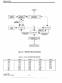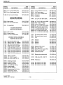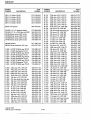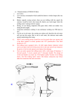
1
" Service Manual
115/230 VAC 25-100 Watts
Part No.: 242- 1 1 00-xxx
Fifth Prrntirig
August 1996
Supersedes 00I - l 100-002
JOHNSON 1100
150-174 MHz REPEATER
SERVICE MANUAL
1151230V AC OPERATION
25- 100 WATT RF OUTPUT
PART NO. 242- 1100-xxx
Copyright@ 1979 by the E.F. Johnson Company
The E.F. Johnson Company designs and manufactures two-way radio equipment to serve a wide variety of communications
needs. E.F. Johnson produces equipment for the mobile telephone and land mobile radio services which include business, industrial, government, public safety, and personal users.
LAND MOBILE PRODUCT WARRANTY
The manufacturer's warranty statement for this product is available from your product supplier or from the E.F. Johnson Company, 299 Johnson Avenue, Box 1249, Waseca, MN 56093-0514. Phone (507) 835-6222.
WARNING
This device complies with Part 15 of the FCC rules. Operation is subject to the condition that this device does not cause harmful
interference. In addition, changes or modification to this equipment not expressly approved by the E.F. Johnson Company could
void the user's authority to operate this equipment (FCC rules, 47CFR Part 15.19).
DO NOT allow the antenna to come close to or touch, the eyes, face, or any exposed body parts while the radio is transmitting.
DO NOT operate the radio near electrical blasting caps or in an explosive atmosphere.
DO NOT operate the radio unless all the radio frequency connectors are secure and any open connectors are properly terminated.
DO NOT allow children to operate transmitter equipped radio equipment.
SAFETY INFORMATION
Proper operation of this radio will result in user exposure below the Occupational Safety and Health Act and Federal Communication Commission limits.
The information in this document is subject to change without notice. E.F. Johnson Company will not be liable for any misunderstanding due to misinformation or errors found in this document.
--
Viking HeadEFJohnson Logo and Call Guard are registered trademarks of the E.F. Johnson Company, a subsidiary of Transcrypt
International, Inc. All other company and/or product names used in this manual are trademarks and/or registered trademarks of
their respective manufacturer.
TABLE OF CONTENTS
1
GENERAL INFORMATION
SCOPEOFMANUAL .......................................................................
1-1
DESCRIPTION ............................................................................ 1.1
REPEATER IDENTIFICATION ..............................................................1.1
JOHNSON CRllOO MODELS ................................................................ 1-1
ACCESSORIES ............................................................................ 1-1
EXTERNALCWIDENTIFIER ................................................................. 1-1
REPEATERCABINETS ......................................................................
1-2
MICROPHONE ............................................................................. 1-2
FACTORY CUSTOMER SERVICE ...........................................................1-2
PRODUCTWARRANm .................................................................... 1-2
FACTORYRETURNS ...................................................................... 1-3
REPLACEMENTPARTS .................................................................... 1-3
2
INSTALLATION
2.1
2.2
2.3
2.4
INTRODUCTION .......................................................................... 2-1
115/230VACOPERATION ..................................................................
2-1
INSTALLATION ...........................................................................
2-1
REPEATER START-UP ..................................................................... 2-1
3
CIRCUIT DESCRIPTION
3.1
3.2
GENERAL ................................................................................ 3-1
RECEIVER ................................................................................ 3-1
3-1
DCPOWERSUPPLY ........................................................................
HELICALFILTER. FIRSTMIXER ............................................................. 3-1
OSCILLATOR TRIPLER. SECOND TRIPLER. INJECTION AMPLIFIER .............................3-1
10.7 MHz CRYSTAL FILTER AND 10.7 MHz AMPLIFIER . . . . . . . . . . . . . . . . . . . . . . . . . . . . . . . . . . . . . . . . . 3-2
SECOND OSCILLATOR. SECOND MIXER .....................................................3-2
FIRST IF AMPLIFIER. SECOND IF AMPLIFIER . . . . . . . . . . . . . . . . . . . . . . . . . . . . . . . . . . . . . . . . . . . . . . . . . 3-2
LIMITERDISCRIMINATOR . . . . . . . . . . . . . . . . . . . . . . . . . . . . . . . . . . . . . . . . . . . . . . . . . . . . . . . . . . . . . . . . . . 3-2
AUDIO PRE.AMPLIFIER. CALL GUARD FILTER . . . . . . . . . . . . . . . . . . . . . . . . . . . . . . . . . . . . . . . . . . . . . . . 3-2
AUDIODRIVER. AUDIOOUTPUT ............................................................ 3-2
SQUELCH AMPLIFIER. SQUELCH FILTER (U202D). SQUELCH GATE . . . . . . . . . . . . . . . . . . . . . . . . . . . . . 3-3
TRANSMITTER ........................................................................... 3 4
DC POWER SUPPLY. TRANSMIT SWITCH . . . . . . . . . . . . . . . . . . . . . . . . . . . . . . . . . . . . . . . . . . . . . . . . . . . . . 3-4
TRANSMITAUDIOSTAGES . . . . . . . . . . . . . . . . . . . . . . . . . . . . . . . . . . . . . . . . . . . . . . . . . . . . . . . . . . . . . . . . . 3 4
TRANSMIT OSCILLATORDOUBLER . . . . . . . . . . . . . . . . . . . . . . . . . . . . . . . . . . . . . . . . . . . . . . . . . . . . . . . . . 3-4
FIRST DOUBLER. SECOND DOUBLER . . . . . . . . . . . . . . . . . . . . . . . . . . . . . . . . . . . . . . . . . . . . . . . . . . . . . . . . 3-5
FIRST RF AMPLIFIER. SECOND RF AMPLIFIER . . . . . . . . . . . . . . . . . . . . . . . . . . . . . . . . . . . . . . . . . . . . . . . . 3-5
PREDRIVER.DRIVER. FINALS ............................................................... 3-6
POWERCONTROL . . . . . . . . . . . . . . . . . . . . . . . . . . . . . . . . . . . . . . . . . . . . . . . . . . . . . . . . . . . . . . . . . . . . . . . . . 3-6
POWERSUPPLY . . . . . . . . . . . . . . . . . . . . . . . . . . . . . . . . . . . . . . . . . . . . . . . . . . . . . . . . . . . . . . . . . . . . . . . . . . 3-6
CONTROLCARD . . . . . . . . . . . . . . . . . . . . . . . . . . . . . . . . . . . . . . . . . . . . . . . . . . . . . . . . . . . . . . . . . . . . . . . . . . 3-7
GENERAL . . . . . . . . . . . . . . . . . . . . . . . . . . . . . . . . . . . . . . . . . . . . . . . . . . . . . . . . . . . . . . . . . . . . . . . . . . . . . . . . . 3-7
TRANSMIT CONTROL CIRCUITS. . . . . . . . . . . . . . . . . . . . . . . . . . . . . . . . . . . . . . . . . . . . . . . . . . . . . . . . . . . . .3-7
CALL GUARD SQUELCH CIRCUITS . . . . . . . . . . . . . . . . . . . . . . . . . . . . . . . . . . . . . . . . . . . . . . . . . . . . . . . . . .3-8
LEVEL ADJUST CARD . . . . . . . . . . . . . . . . . . . . . . . . . . . . . . . . . . . . . . . . . . . . . . . . . . . . . . . . . . . . . . . . . . . . . 3-9
GENERAL . . . . . . . . . . . . . . . . . . . . . . . . . . . . . . . . . . . . . . . . . . . . . . . . . . . . . . . . . . . . . . . . . . . . . . . . . . . . . . . . . 3-9
9.6VREGULATOR . . . . . . . . . . . . . . . . . . . . . . . . . . . . . . . . . . . . . . . . . . . . . . . . . . . . . . . . . . . . . . . . . . . . . . . . . . 3-9
TRANSMITAUDIOCIRCUITS(REMOTEKEY1NG). . . . . . . . . . . . . . . . . . . . . . . . . . . . . . . . . . . . . . . . . . . . . 3-9
3.3
3.4
3.5
3.6
.
TABLE OF CONTENTS
RECEIVE CALL GUARD AUDIO CIRCUITS ................................................... 3-9
ENCODED CALL GUARD AUDIO ...........................................................3-10
TRANSMIT AUDIO CIRCUITS (LOCAL KEYING) ............................................. 3-11
SQUELCH ADJUSTMENT ..................................................................3-11
CALL GUARD SQUELCH CARD ............................................................3. 11
GENERAL . . . . . . . . . . . . . . . . . . . . . . . . . . . . . . . . . . . . . . . . . . . . . . . . . . . . . . . . . . . . . . . . . . . . . . . . . . . . . . . 3-11
DECODEAUDIO MPUT ...................................................................3-11
DECODE BUFFEWAMPLIFIER (U503A). BANDPASS FILTER (U503BAJ503C) ..................... 3-11
THRESHOLD DETECTOR (U503D). BANDPASS FILTER (U503BAJ503C) . . . . . . . . . . . . . . . . . . . . . . . . . 3-12
ENCODE SWITCH (Q504) AND AUDIO SWITCH (S500) . . . . . . . . . . . . . . . . . . . . . . . . . . . . . . . . . . . . . . . . 3-12
ENCODEMODE .......................................................................... 3-12
SERVICING
GENERAL . . . . . . . . . . . . . . . . . . . . . . . . . . . . . . . . . . . . . . . . . . . . . . . . . . . . . . . . . . . . . . . . . . . . . . . . . . . . . . . . .4-1
PERIODICCHECKS . . . . . . . . . . . . . . . . . . . . . . . . . . . . . . . . . . . . . . . . . . . . . . . . . . . . . . . . . . . . . . . . . . . . . . . . 4-1
VISUALINSPECTION ...................................................................... 4-1
SCHEMATICS AND COMPONENT LAYOUTS . . . . . . . . . . . . . . . . . . . . . . . . . . . . . . . . . . . . . . . . . . . . . . . . . 4-1
REPLACEMENTPARTS . . . . . . . . . . . . . . . . . . . . . . . . . . . . . . . . . . . . . . . . . . . . . . . . . . . . . . . . . . . . . . . . . . . . 4-1
SERVICEANDALIGNMENTTOOLS ......................................................... 4-1
DRAWERREMOVAL . . . . . . . . . . . . . . . . . . . . . . . . . . . . . . . . . . . . . . . . . . . . . . . . . . . . . . . . . . . . . . . . . . . . . . 4-1
INTEGRATED CIRCUIT SERVICING ........................................................4. 1
CMOSHANDLINGPRECAUTIONS ........................................................... 4-1
SERVICINGTECHNIQUES . . . . . . . . . . . . . . . . . . . . . . . . . . . . . . . . . . . . . . . . . . . . . . . . . . . . . . . . . . . . . . . . . . 4-2
TRANSISTOR SERVICING .................................................................. 4.2
REPLACING TRANSISTORS SOLDERED TO MICROSTRIP . . . . . . . . . . . . . . . . . . . . . . . . . . . . . . . . . . . . . . 4-2
LOCALIZING PROBLEM TO A DEFECTIVE ASSEMBLY ......................................4.3
INTRODUCTION .......................................................................... 4-3
RECEIVETROUBLESHOOTING ............................................................4-3
DCSUPPLYVOLTAGES .................................................................... 4-3
SQUELCH . . . . . . . . . . . . . . . . . . . . . . . . . . . . . . . . . . . . . . . . . . . . . . . . . . . . . . . . . . . . . . . . . . . . . . . . . . . . . . . . 4-3
AUDIO . . . . . . . . . . . . . . . . . . . . . . . . . . . . . . . . . . . . . . . . . . . . . . . . . . . . . . . . . . . . . . . . . . . . . . . . . . . . . . . . . . . 4-3
LIMITER.DISCRIMINATOR, FIRST AND SECOND IF . . . . . . . . . . . . . . . . . . . . . . . . . . . . . . . . . . . . . . . . . . . 4-4
SECOND MIXEWSECOND OSCILLATOR / 10.7 MHz AMPLIFIER . . . . . . . . . . . . . . . . . . . . . . . . . . . . . . . . . 4-4
OSCILLATOR-TRIPLER/I?IIPLER/INJECTION
AMPLIFIERIFIRST MIXER ......................... 4-5
TRANSMIT TROUBLESHOOTING...........................................................4.5
GENERAL . . . . . . . . . . . . . . . . . . . . . . . . . . . . . . . . . . . . . . . . . . . . . . . . . . . . . . . . . . . . . . . . . . . . . . . . . . . . . . . . 4-5
DCSUPPLYVOLTAGE . . . . . . . . . . . . . . . . . . . . . . . . . . . . . . . . . . . . . . . . . . . . . . . . . . . . . . . . . . . . . . . . . . . . . 4-5
AUDIO . . . . . . . . . . . . . . . . . . . . . . . . . . . . . . . . . . . . . . . . . . . . . . . . . . . . . . . . . . . . . . . . . . . . . . . . . . . . . . . . . . . 4-5
OSCLLATOR/DOUBLER, FIRST-SECOND DOUBLER . . . . . . . . . . . . . . . . . . . . . . . . . . . . . . . . . . . . . . . . . . 4-5
FIRST-SECOND RF AMPLIFIERS, PREDRIVER ................................................ 4-6
POWERCONTROL . . . . . . . . . . . . . . . . . . . . . . . . . . . . . . . . . . . . . . . . . . . . . . . . . . . . . . . . . . . . . . . . . . . . . . . . . 4-6
POWER AMPLIFIER TROUBLESHOOTING . . . . . . . . . . . . . . . . . . . . . . . . . . . . . . . . . . . . . . . . . . . . . . . . . . 4-7
COMPONENTREPLACEMENT . . . . . . . . . . . . . . . . . . . . . . . . . . . . . . . . . . . . . . . . . . . . . . . . . . . . . . . . . . . . . . 4-7
POWER AMPLIFIER PC BOARD REMOVAL . . . . . . . . . . . . . . . . . . . . . . . . . . . . . . . . . . . . . . . . . . . . . . . . . . . 4-7
CIRCUITPROTECTION. . . . . . . . . . . . . . . . . . . . . . . . . . . . . . . . . . . . . . . . . . . . . . . . . . . . . . . . . . . . . . . . . . . . . 4-7
TESTINGQ901 . . . . . . . . . . . . . . . . . . . . . . . . . . . . . . . . . . . . . . . . . . . . . . . . . . . . . . . . . . . . . . . . . . . . . . . . . . . . 4-8
TESTINGQ902, Q903ANDQ904 . . . . . . . . . . . . . . . . . . . . . . . . . . . . . . . . . . . . . . . . . . . . . . . . . . . . . . . . . . . . . 4-8
LEVEL ADJUST, CONTROL AND CALL GUARD SQUELCH CARDS . . . . . . . . . . . . . . . . . . . . . . . . . . . .4.8
GENERAL . . . . . . . . . . . . . . . . . . . . . . . . . . . . . . . . . . . . . . . . . . . . . . . . . . . . . . . . . . . . . . . . . . . . . . . . . . . . . . . . 4-8
CONTROL CARD NOR GATE (U602) OPERATION . . . . . . . . . . . . . . . . . . . . . . . . . . . . . . . . . . . . . . . . . . . . . 4-8
TABLE OF CONTENTS
4.10
CHECKING RECEIVE DESENSITIZATION....................................................4.9
INTRODUCTION ............................................................................4-9
CAPACITNECOUPLER ..................................................................... 4-9
TESTPROCEDURE ......................................................................... 4-9
LOCALIZING CAUSE OF DESENSITIZATION .................................................. 4-9
DETERMINING EFFECTIVE SENSITIVITY . . . . . . . . . . . . . . . . . . . . . . . . . . . . . . . . . . . . . . . . . . . . . . . . . . 4-9
5
ALIGNMENT AND PERFORMANCE TESTS
5.1
5.2
GENERAL ................................................................................ 5-1
RECEIVERALIGNMENT ...................................................................5-1
FIRST OSCILLATOR/TRIPLER. INJECTION AMPLIFIER ......................................... 5-1
FIRST OSCILLATOR FREQUENCY ADJUSTMENT .............................................. 5-1
5-1
FRONTENDANDIFAMPLIFIERS ............................................................
DISCRIMINATOR . . . . . . . . . . . . . . . . . . . . . . . . . . . . . . . . . . . . . . . . . . . . . . . . . . . . . . . . . . . . . . . . . . . . . . . . . . 5-2
TRANSMITTERALIGNMENT . . . . . . . . . . . . . . . . . . . . . . . . . . . . . . . . . . . . . . . . . . . . . . . . . . . . . . . . . . . . . . 5-2
0SCILLATOR.DOUBLER. MULTIPLIERS ...................................................... 5-2
SECONDRFAMPLIFIER ....................................................................5-2
PRELIMINARY DEVIATION ADJUSTMENT....................................................
5-3
TRANSMITDEVIATION . . . . . . . . . . . . . . . . . . . . . . . . . . . . . . . . . . . . . . . . . . . . . . . . . . . . . . . . . . . . . . . . . . . . .5-3
CALLGUARDDEVIATION . . . . . . . . . . . . . . . . . . . . . . . . . . . . . . . . . . . . . . . . . . . . . . . . . . . . . . . . . . . . . . . . . . 5-3
CALL GUARD TONE FREQUENCY ADJUSTMENT.............................................. 5-3
RECEIVER PERFORMANCE TEST ..........................................................
5-4
Q U I E T I N G S E N S I W m .................................................................... 5-4
SINADSENSITIVITY ....................................................................... 5-4
SQUELCHSENSITIVITY .................................................................... 5-5
CALLGUARDSQUELCH .................................................................... 5-5
TRANSMIT PERFORMANCE TEST .......................................................... 5.5
TRANSMITFREQUENCY .................................................................... 5-5
TRANSMITPOWEROUTPUT ................................................................ 5-5
TRANSMITDEVIATION .....................................................................5-5
CALLGUARDSQUELCH . . . . . . . . . . . . . . . . . . . . . . . . . . . . . . . . . . . . . . . . . . . . . . . . . . . . . . . . . . . . . . . . . . . . 5-5
4.9
5.3
5.4
5.5
6
PARTSLIST
11OOREPEATER150-160MHz . . . . . . . . . . . . . . . . . . . . . . . . . . . . . . . . . . . . . . . . . . . . . . . . . . . . . . . . . . . . . . . . 6-1
1100 REPEATER 160- 174 MHz . . . . . . . . . . . . . . . . . . . . . . . . . . . . . . . . . . . . . . . . . . . . . . . . . . . . . . . . . . . . . . . . 6-1
RECEIVER. . . . . . . . . . . . . . . . . . . . . . . . . . . . . . . . . . . . . . . . . . . . . . . . . . . . . . . . . . . . . . . . . . . . . . . . . . . . . . . . -6-1
EXCITER .................................................................................. 6-5
POWERAMPLIFIER ........................................................................ 6-9
25APOWERSUPPLY . . . . . . . . . . . . . . . . . . . . . . . . . . . . . . . . . . . . . . . . . . . . . . . . . . . . . . . . . . . . . . . . . . . . . . 6-11
RECEIVERHARNESS . . . . . . . . . . . . . . . . . . . . . . . . . . . . . . . . . . . . . . . . . . . . . . . . . . . . . . . . . . . . . . . . . . . . . . 6-12
EXCITERHARNESS . . . . . . . . . . . . . . . . . . . . . . . . . . . . . . . . . . . . . . . . . . . . . . . . . . . . . . . . . . . . . . . . . . . . . . . 6-12
FILTERCOVERASSEMBLY . . . . . . . . . . . . . . . . . . . . . . . . . . . . . . . . . . . . . . . . . . . . . . . . . . . . . . . . . . . . . . . . 6-12
CARDRACKASSEMBLY . . . . . . . . . . . . . . . . . . . . . . . . . . . . . . . . . . . . . . . . . . . . . . . . . . . . . . . . . . . . . . . . . . . 6-13
TEST CARD . . . . . . . . . . . . . . . . . . . . . . . . . . . . . . . . . . . . . . . . . . . . . . . . . . . . . . . . . . . . . . . . . . . . . . . . . . . . . - 6 -13
CONTROL CARD . . . . . . . . . . . . . . . . . . . . . . . . . . . . . . . . . . . . . . . . . . . . . . . . . . . . . . . . . . . . . . . . . . . . . . . . . - 6 -13
LEVELCARD . . . . . . . . . . . . . . . . . . . . . . . . . . . . . . . . . . . . . . . . . . . . . . . . . . . . . . . . . . . . . . . . . . . . . . . . . . . . . 6-15
TYPE-ACALLGUARDCA RD . . . . . . . . . . . . . . . . . . . . . . . . . . . . . . . . . . . . . . . . . . . . . . . . . . . . . . . . . . . . . . . 6-16
4-TONE CALL GUARD CARD . . . . . . . . . . . . . . . . . . . . . . . . . . . . . . . . . . . . . . . . . . . . . . . . . . . . . . . . . . . . . . . 6-17
CWIDCARD . . . . . . . . . . . . . . . . . . . . . . . . . . . . . . . . . . . . . . . . . . . . . . . . . . . . . . . . . . . . . . . . . . . . . . . . . . . . . . 6-19
TABLE OF CONTENTS
7
SCHEMATIC DIAGRAMS AND COMPONENT LAYOUTS
ACCESSORIESIOPTIONS ....................................................................
1-2
CALLGUARDFREQUENCIES ...............................................................
2-2
APPROXlMATE LOGIC LEVELS .............................................................4.2
SQUELCHVOLTAGES ......................................................................
4-3
RECEIVER AUDIO SIGNAL TRACING ........................................................4-4
IF AND LIMITER/DISCRIMINATOR VOLTAGES ...............................................44.
.
10.7 MHz UNMODULATED INJECTION POINTS . . . . . . . . . . . . . . . . . . . . . . . . . . . . . . . . . . . . . . . . . . . . . . .4-4
2ndMIXER/2ndOSC/10.7MHzAMP ...........................................................
4-5
INJECTION STRIP AND FIRST MIXER . . . . . . . . . . . . . . . . . . . . . . . . . . . . . . . . . . . . . . . . . . . . . . . . . . . . . . . .4.5
TRANSMITTER AUDIO SIGNAL TRACING ....................................................4.6
POWER CONTROL VOLTAGES ..............................................................4.6
EXCITER VOLTAGE READINGS .............................................................4.7
TEST PANEL SWITCH POSITIONS ...........................................................
5.1
C271VALUES .............................................................................
5-1
C325VALUES .............................................................................
5-2
CALLGUARDRANGEJUMPERS .............................................................5-4
LIST OF FIGURES
REPEATERBLOCKDIAG RAM .............................................................. 2-2
RECEIVERBLOCKDIAGRAM ..............................................................3-3
TRANSMITTER BLOCK DIAGRAM . . . . . . . . . . . . . . . . . . . . . . . . . . . . . . . . . . . . . . . . . . . . . . . . . . . . . . . . . . 3-5
CONTROL CARD BLOCK DIAGRAM . . . . . . . . . . . . . . . . . . . . . . . . . . . . . . . . . . . . . . . . . . . . . . . . . . . . . . . . . 3-8
LEVEL ADJUST CARD BLOCK DIAGRAM ................................................... 3-10
CALLGUARDCARDBLOCKDIAGRAM .................................................... 3-12
MICROPHONESUBSTITUTE ................................................................4-6
RECEIVER DESENSE TEST SETUP........................................................... 4-9
RECEIVER TROUBLESHOOTING FLOWCHART .............................................. 4-10
TRANSMITTER TROUBLESHOOTING FLOWCHART .......................................... 4-11
RECEIVERTESTSETUP . . . . . . . . . . . . . . . . . . . . . . . . . . . . . . . . . . . . . . . . . . . . . . . . . . . . . . . . . . . . . . . . . . . . 5-1
TRANSMITTESTSETUP ................................................................... 5-2
CALLGUARDCARDALIGNMENTPOINTS . . . . . . . . . . . . . . . . . . . . . . . . . . . . . . . . . . . . . . . . . . . . . . . . . . . 5-4
RECEIVER ALIGNMENT POINTS . . . . . . . . . . . . . . . . . . . . . . . . . . . . . . . . . . . . . . . . . . . . . . . . . . . . . . . . . . . . 5-6
TRANSMITTERALIGNMENTPOINTS . . . . . . . . . . . . . . . . . . . . . . . . . . . . . . . . . . . . . . . . . . . . . . . . . . . . . . . . 5-6
CARDRACKWIRINGDIAGRAM . . . . . . . . . . . . . . . . . . . . . . . . . . . . . . . . . . . . . . . . . . . . . . . . . . . . . . . . . . . .7-1
CARD RACK BLOCK DIAGRAM . . . . . . . . . . . . . . . . . . . . . . . . . . . . . . . . . . . . . . . . . . . . . . . . . . . . . . . . . . . . . 7-2
25A POWER SUPPLY SCHEMATIC........................................................... 7-3
25A POWER SUPPLY COMPONENT LAYOUT (TOP) ........................................... 7-3
25A POWER SUPPLY COMPONENT LAYOUT (BOTI'OM) . . . . . . . . . . . . . . . . . . . . . . . . . . . . . . . . . . . . . . . 7-3
TESTSWITCHSCHEMATIC . . . . . . . . . . . . . . . . . . . . . . . . . . . . . . . . . . . . . . . . . . . . . . . . . . . . . . . . . . . . . . . . . 7-3
RECEIVER BOARD COMPONENT LAYOUT . . . . . . . . . . . . . . . . . . . . . . . . . . . . . . . . . . . . . . . . . . . . . . . . . . . 7-4
FRONTENDSTRIPCOMPONENTLAYO UT . . . . . . . . . . . . . . . . . . . . . . . . . . . . . . . . . . . . . . . . . . . . . . . . . . . 7-4
RECEIVER SCHEMATIC DIAGRAM . . . . . . . . . . . . . . . . . . . . . . . . . . . . . . . . . . . . . . . . . . . . . . . . . . . . . . . . . . 7-5
TRANSMITTER BOARD COMPONENT LAYOUT . . . . . . . . . . . . . . . . . . . . . . . . . . . . . . . . . . . . . . . . . . . . . . 7-6
POWER CONTROL BOARD COMPONENT LAYOUT . . . . . . . . . . . . . . . . . . . . . . . . . . . . . . . . . . . . . . . . . . . 7-6
TRANSMITTER SCHEMATIC DIAGRAM . . . . . . . . . . . . . . . . . . . . . . . . . . . . . . . . . . . . . . . . . . . . . . . . . . . . . 7-7
POWER AMPLIFIER COMPONENT LAY OUT . . . . . . . . . . . . . . . . . . . . . . . . . . . . . . . . . . . . . . . . . . . . . . . . . . 7-8
POWER AMPLIFIER AND FILTER COVER ASSEMBLY ......................................... 7-9
TYPE-ACALLGUARDCOMPONENTLAYOUT. . . . . . . . . . . . . . . . . . . . . . . . . . . . . . . . . . . . . . . . . . . . . . 7-10
TYPE-ACALLGUARDSCHEMATIC ........................................................7-11
CONTROL CARD COMPONENT LAYOUT . . . . . . . . . . . . . . . . . . . . . . . . . . . . . . . . . . . . . . . . . . . . . . . . . . . 7-12
CONTROLCARDSCHEMATIC ............................................................. 7-13
LEVEL ADJUST CARD COMPONENT LAY OUT . . . . . . . . . . . . . . . . . . . . . . . . . . . . . . . . . . . . . . . . . . . . . . . 7-14
TABLE OF CONTENTS
'
7-20
7-2 1
'-22
1-23
7-24
.
.
LEVEL ADJUST CARD SCHEMATIC ........................................................ 7-15
4-TONE CALL GUARD COMPONENT LAYOUT............................................... 7-16
4-TONE CALL GUARD SCHEMATIC ........................................................ 7-17
CW IDENTIFIER COMPONENT LAYOUT ...............: .................................... 7-18
CW IDENTIFIER SCHEMATIC .............................................................. 7-19
LIST OF TABLES
ACCESSORIESIOPTIONS ....................................................................1-2
CALLGUARDFREQUENCIES ...............................................................2-2
APPROXIMATE LOGIC LEVELS .............................................................4.2
SQUELCHVOLTAGES ......................................................................4-3
RECEIVER AUDIO SIGNAL TRACING ........................................................4.4
IF AND LIMITERIDISCRIMINATOR VOLTAGES ...............................................4.4
10.7 MHz UNMODULATED INJECTION POINTS ................................................4.4
2nd MIXERl2nd OSCl10.7 MHz AMP ...........................................................4.5
INJECTION STRIP AND FIRST MIXER ........................................................4.5
TRANSMITTER AUDIO SIGNAL TRACING ....................................................4.6
POWER CONTROL VOLTAGES .............................................................-4-6
EXCITERVOLTAGEREADINGS .............................................................4-7
TESTPANELSWITCHPOSITIONS ...........................................................5-1
C271VALUES .............................................................................5-1
C325VALUES .............................................................................5-2
CALLGUARDRANGEJUMPERS .............................................................5-4
TABLE OF CONTENTS
GENERAL INFORMATION
SECTION 1 GENERAL INFORMATION
1.1 SCOPE OF MANUAL
1.4 JOHNSON CR1100 MODELS
This service manual includes installation, circuit
description, servicing, and alignment information for
the Johnson 1100 VHF repeater, Part No. 242- 1100-
The following breakdown shows the part number
scheme used for the Johnson CR1100 models.
XXX.
242- 1 1 W X X X
TTT
1.2 DESCRIPTION
4
The Johnson 1100 is a VHF FM repeater which
operates on a single channel in the 150-174 MHz
range. It is completely solid state and the transmitter
is rated at 100 watts RF power output continuous duty.
The output from the duplexer (if equipped) is approximately 70 watts.
The 1100 can be ordered as a single-user or a
community repeater. When used in a single-user configuration, the repeater is activated by the receiver's
squelch circuitry or by a tone if the unit is equipped
with the Retransmit Call Guard@card.
The tone remote console (Part No. 250-45xxxxx) functions as a control point or base station when
used with the repeater.
When used in the community repeater configuration, the repeater is activated by any one of 16 possible
Call Guard tones. Each Call Guard card contains four
tunable Call Guards (see Table 1-1).
1.3 REPEATER IDENTIFICATION
The serial number is printed on an adhesive
backed cloth attached to the inside of the cabinet. The
following table shows a breakdown of an identification number.
Revision
1
1100
A
Manufacture
o1,
Month
oLeU
12345
A = Waseca
[l] WITH DUPLEXER
[2] WITH TONE REMOTE
1.5 ACCESSORIES
Refer to Table 1-1 for a listing of CR1100
repeater accessories/optionsand their part numbers.
1.5.1 EXTERNAL CW IDENTIFIER
The CWID is a separate PC board option that provides automatic international Morse Code station call
sign identification by superimposing coded audio onto
the transmit modulation. If voice communication is in
process, the ID is not transmitted until the repeater
unkeys. If the ID is being transmitted, the repeater can
be accessed and the voice communication will be
heard over the ID.
U701 is included in the kit to upgrade the software if necessary. Revision 208 or later software is
required with the CWID.
Warranty
;
0-BASE STATION
1 -STANDARD UNIT
2-STANDARD UNIT [l]
3-STANDARD UNIT (21
1
The PROM can be factory programmed or programmed with the PROM Programmer 11, Part No.
250-3020-200.
August 1996
Part No. 001-1 100-003
GENERAL INFORMATION
Table 1-1 ACCESSORIESIOPTIONS
Part Number
Description
522-oxxx-xxx
I'ransmit 2.5 PPM TCXO [I]
522- 1xxx-xxx
Zeceive 2.5 PPM TCXO [I]
52 1-Oxxx-xxx
I'ransmit 5 PPM TCXO [I]
521-6xxx-xxx
Receive 5 PPM TCXO [1]
023-3823-080
Receiver Shield Kit
023-3823-340
rest Panel
023-3823-050
$-Tone Call Guard Squelch
023-3823-056
Type-A Call Guard Squelch
023-3988-001
Power Failure Alarm
023-3823-330
CW Identifier Card
250-0740-200
Heavy Duty Microphone
023-3824-003
60" Indoor Cabinet
023-4061-001
43" Outdoor Cabinet
023-4061-002
60" Outdoor Cabinet
Duplexer
532-4001-006
150-162 MHz
532-4001-013
162-174 MHz
[I] The last six digits are determined by the frequency in
MHz.
This information may also be requested by phone
from the Warranty Department as described in Section
1.7. The Warranty Department may also be contacted
for Warranty Service Reports, claim forms, or any
questions concerning warranties or warranty service
by dialing (507) 835-6222.
1.7 FACTORY CUSTOMER SERVICE
The Customer Service Department of the E.F.
Johnson Company provides customer assistance on
technical problems and the availability of local and
factory repair facilities. Regular Customer Service
hours are 7:30 a.m. - 5:30 p.m. Central Time,
Monday - Friday. The Customer Service Department
can be reached using one of the following telephone
numbers:
Toll-Free: (800) 328-3911
(From within continental United States only)
International: (507) 835-6911
FAX: (507) 835-6969
1.5.2 REPEATER CABINETS
The standard 30-inch cabinet does not have additional room for accessories. The 43" or 60" cabinets
are used when accessories, such as a duplexer are
installed. The outdoor cabinet consists of three panels
which install around the indoor cabinet to make it
weather resistant.
1.5.3 MICROPHONE
This is a high-impedance microphone used for
repeater testing.
1.6 PRODUCT WARRANTY
The warranty statement for this transceiver is
available from your product supplier or from the
Warranty Department
Transcrypt International, Inc.
299 Johnson Avenue,
Box 1249,
Waseca, MN 56093- 0514
August 1996
Part No. 001 -1 100-003
E-Mail: First InitiaVLast [email protected]
(You need to know the name of the person you want to
reach. Example: [email protected])
NOTE: Emergency 24-hour technical support is also
available at the 800 and preceding numbers during o f
hours, holidays, and weekends.
When your call is answered at E.F. Johnson Company, you will hear a brief message informing you of
numbers that can be entered to reach various departments. This number may be entered during or after the
message using a tone-type telephone. If you have a
pulse-type telephone, wait until the message is finished and an operator will come on the line to assist
you. When you enter some numbers, another number
is requested to further categorize the type of information you need.
You may also contact the Customer Service
Department by mail. Please include all information
that may be helpful in solving your problem. The
mailing address is as follows:
-
GENERAL INFORMATION
Transcrypt International, Inc.
Customer Service Department
299 Johnson Avenue
P.O. Box 1249
Waseca, MN 56093-0514
1.8 FACTORY RETURNS
Repair service is normally available through local
authorized E.F. Johnson Land Mobile Radio Service
Centers. If local service is not available, the equipment
can be returned to the factory for repair. However, it is
recommended that you contact the Customer Service
Department before returning equipment because a service representative may be able to suggest a solution
to the problem so that return of the equipment would
not be necessary.
Be sure to fill out a Factory Repair Request Form
#271 for each unit to be repaired, whether it is in or
out of warranty. These forms are available free of
charge by calling the repair lab (see Section 1.7) or by
requesting them when you send a unit in for repair.
Clearly describe the difficulty experienced in the space
provided and also note any prior physical damage to
the equipment. Then include a form in the shipping
container with each unit. Your telephone number and
contact name are important because there are times
when the technicians have specific questions that need
to be answered in order to completely identify and
repair a problem.
When returning equipment for repair, use a PO
number or some other reference number on your
paperwork in case you need to call the repair lab about
your unit. These numbers are referenced on the repair
order and it makes it easier and faster to locate your
unit in the lab.
Return Authorization (RA) numbers are not necessary unless you have been given one by the Field
Service Department. RA numbers are required for
exchange units or if the Field Service Department
wants to be aware of a specific problem. If you have
been given an RA number, reference this number on
the Factory Repair Request Form sent with the unit.
The repair lab will then contact the Field Service
Department when the unit arrives.
1.9 REPLACEMENT PARTS
E.F. Johnson replacement parts can be ordered
directly from the Service Parts Department. To order
parts by phone, dial the toll-free number as described
in Section 1.7. When ordering, please supply the part
number and quantity of each part ordered. E.F.
Johnson dealers also need to give their account number. If there is uncertainty about the part number,
include the designator (C 112, for example) and the
model number of the equipment the part is from.
You may also send your order by mail or FAX.
The mailing address is as follows and the FAX number
is shown in Section 1.7.
E.F. Johnson Company
Service Parts Department
299 Johnson Avenue
P.O. Box 1249
Waseca, MN 56093-0514
1.10 INTERNET HOME PAGE
The E.F. Johnson Company has a home page on
the World Wide Web that can be accessed for information on such things as products, systems, and regulations. The address is http:Nwww.transcrypt.com.
August 1996
Part No. 001-1100-003
GENERAL INFORMATION
August 1996
Part No. 001 -1 100-003
INSTALLATION
SECTION 2 INSTALLATION
2.1 INTRODUCTION
2.3 INSTALLATION
Although this equipment is carefully aligned at
the factory, shipment can upset some of the adjustments so pre-installation testing is recommended.
Complete the tests listed in the "Performance Tests",
Sections 5.4 and 5.5.
1. Install the antenna coaxial cable through the access
holes in the front or back baseplates of the repeater
cabinet. Connect the cable to the duplexer or to the
transmitter and receiver, depending on the type of
installation. Connect the power supply to AC
power.
Site preparation and antenna installation is not
within the scope of this manual. Refer to the "Dealer
Guide To Site Preparation", Part No. 004-8000-100,
for preliminary installation requirements. Factory
installation of repeaters is available. Contact your
sales representative for more information.
NOTE: Because most repeater installations require
several hundred feet of coaxial cable, it is very important that the cable be a high quality product. Failure
to use a high quality cable may result in large power
losses and poor repeater perSonnance.
2.4 REPEATER START-UP
2.2 1151230V AC OPERATION
Connect the AC power cord and set the various
controls on the cards as follows:
Call Guard Card
CAUTION
Do not connect the power supply to AC power
until an antenna or dummy load has been connected
to the antenna jack. The transmitter may momentarily
key and damage to the power ampliBer could result.
Set the Encode switch to OFF and the switches
on the PC board to ON if the respective Call Guard
squelch is being used.
Control Card
Set Repeat switch to ON and the Access switch
to TONE.
The same power supply can be used for 115 or
230V AC power sources. If the power supply needs to
be converted to operate on the other power source,
rewire the transformer and change fuse F1 as shown
on the schematic and wiring diagrams in the back of
this manual. However, if a change between 50 and 60
Hz power sources is necessary, a different transformer
is required.
Level Card
The Call Guard Level control and Transmit
Audio Level control are factory set or are adjusted
during repeater alignment. Adjust the Local audio
control as desired and adjust the Squelch Adjust control so the squelch opens and the transmitter keys
when the desired signal level is received.
August 1996
Part No. 001-1 100-003
INSTALLATION
ANTENNA
I
POWER
+AMPLIFIER
%,TX
DUPLEXER
(OPTIONAL)
RX
RF
DC
POWER
CONTROL
RF
-
DC
PANEL
EXCITER
>*
RECEIVER
AUDIO AND DC
CONTROL
ONE REMOTE RACK
(OPTIONAL)
Figure 2-1 REPEATER BLOCK DIAGRAM
Table 2-1 CALL GUARD FREQUENCIES
I
FREQ
FREQ
FREQ
FREQ
FREQ
203.5
21 0.7
218.1
225.7
233.6
241.8
250.3
August 1996
Part No. 001-1 100-003
-
INSTALLATION
CRllOO SPECIFICATIONS
The following are general specifications intended for use in testing and servicing this repeater. For current advertised specifications, refer to the Marketing Specifications sheet. Specifications are subject to change without notice.
GENERAL
Frequency Range
Channels
Transrnit/Receive Separation
Dimensions
Microphone
Power Source
FCC Compliance
Duty Cycle
Circuit Protection
150-174 MHz
1
5 MHz
43"H x 22"W x 15"D
Optional HD for local operation and test
115V ACl230V AC
Parts 15,21,74,90 and 16F3
Continuous
25A fuse
RECEIVER
Sensitivity
Selectivity
Squelch Sensitivity
Spurious
Image Rejection
Intermodulation
Audio Power Output
Hum and Noise
Frequency Stability
Optional
Input Impedance
Speaker impedance
0.35 mV (12 dB SINAD)
-90 dB
0.25 mV
-100 dB
-100 dB
-80 dB
0.5 Watt (local)
-60 dB (squelched)
It5 PPM -22°F to +140°F
k2.5 PPM -22°F to +140°F
50 Ohms (nominal)
8 Ohms
TRANSMITTER
RF Power Output
Duty Cycle
Spurious and Harmonic Emissions
Modulation
FM Hum and Noise
Frequency Stability
Optional
Audio distortion
Load Impedance
100 Watts
Continuous
-70 dB
16KOF3E: +5 kHz at 77"F/100% at 1 kHz
-50 dB minimum
+J PPM -20°F to +140°F
e . 5 PPM -20°F to +140°F
5% at 1 kHz (23 kHz deviation)
50 Ohms
INSTALLATION
CIRCUIT DESCRIPTION
SECTION 3 CIRCUIT DESCRIPTION
3.1 GENERAL
3.2.3 OSCILLATOR TRIPLER, SECOND TRIPLER, INJECTION AMPLIFIER
The Johnson 1100 is a VHF full duplex multitone repeater (see Figure 2-1). The unit is powered by
a 1151230V AC power supply. The incoming signal is
fed from the receive section of the duplexer to the
receiver. The audio output of the receiver is then fed
to the card rack. A portion of the Card Rack processes
the audio and turns on the exciter. The RF output of
the exciter is coupled to the power amplifier and to the
optional duplexer and the antenna. The repeater can
also be controlled by the optional tone remote console.
Refer to the appropriate schematic diagram or block
diagram while following the circuit description.
Parts are included on the circuit board for two
channel operation, however, only channel 1 is operational. This has been done by hard wiring the emitter
circuit of Q211 to ground.
The oscillator tripler is a modified Colpitts circuit
with the collector of Q211 tuned to the third harmonic
of the crystal frequency. The oscillator output frequency is tuned by R208 and T209. A passive temperature compensation scheme is used with thermistor RT201 controlling the effective capacitance of
C291 which establishes the temperature compensation of the oscillator.
3.2 RECEIVER
3.2.1 DC POWER SUPPLY
NOTE: Crystal compensating capacitor C291 is a factory selected part and is shipped with the crystal.
DC power is applied to the receiver 15.7V DC
line at 5200, pin 35. This line supplies power to the
audio output stages, 9.1V regulator, first mixer, 10.7
MHz IF amplifier, and the audio output stages. Filtering is provided by C 1, C2, C260, L206, C296, L212,
C297, L213 and C299. A regulated 9.1V is supplied
to the remainder of the receiver by Zener diode
CR209.
Frequency adjustment is provided at C269 and
the range of adjustment can be extended by changing
C271 (see Section 5.2.2).
The first oscillator crystal frequency can be determined by the following formula:
3.2.2 HELICAL FILTER, FIRST MIXER
Crystal Freq. = (Chnl Freq f 10.7 MHz) + 9
The incoming on-channel signal is coupled
through a 5-section helical resonator and L106 to the
gate of first mixer Q101. The individual cavities are
tuned by C101-C105. These variable capacitors represent the variable spacing between the ends of their
respective coils and ground. The size and shape of the
aperture between cavities determine the degree of coupling and bandpass characteristics.
The oscillator output circuit is coupled by T208
and T209 to the base of second tripler Q213 through
capacitor C281. The tripler output signal is then coupled through transformer T210 and capacitor C286 to
the base of injection amplifier Q102. A tripler test
voltage is rectified by CR212 and coupled to TP204.
The tripler output is tuned by T210.
An impedance match between the helical resonators and the gate of QlOl is provided by L106 and
C106. First mixer QlOl mixes the incoming signal
with the output of injection amplifier Q102.
The signal from injection amplifier Q102 is coupled to the source of first mixer Q101. The output of
Q102 is tuned by C108 and C109. A test voltage is
rectified by CRlOl and coupled to TP205.
3-1
August 1996
Part No. 001-1100-003
CIRCUIT DESCRIPTION
3.2.4 10.7MHz CRYSTAL FILTER AND 10.7
90" phase shift audio recovery process is used. Inductor T205 adjusts the detector and is tuned for maximum undistorted audio output.
MHz AMPLIFIER
The output of QlOl is tuned to 10.7 MHz, the
difference of the incoming signal frequency and the
output frequency of injection amplifier 4102. This
difference frequency is fed through a length of coax,
L202 and C201 to the input of 2-pole crystal filter
2202. The crystal filter has a bandwidth o f f 5 kHz at
the 3 dB points. The output of 2202 is coupled
through C202, T201 and C298 to the base of
10.7 MHz IF amplifier 4215.
3.2.8 AUDIO PRE-AMPLIFIER, CALL GUARD
FILTER
Detected audio from U202 is coupled through
C235 to the de-emphasis network C230, C255, C237,
R233, R234 and R232. This network provides a 6 dB
per octave de-emphasis from 300-3000 Hz. The gain
of U202A is determined by the ratio of the feedback
resistance and its input resistance. The feedback path
contains C247, used to roll off amplification of frequency over 3 kHz.
The output of 4215 is taken off the collector and
coupled through R295 to crystal filter 2201. An
impedance match between 4215 and 2201 is provided
by R295. This crystal filter has a bandwidth of
15 kHz at the 6 dB points.
The output of U202A is coupled by C252 and
C254 to the inverting input of Call Guard filter
U202B. The components make U202A act as a highpass filter with a low frequency roll-off of approximately 300 Hz to remove Call Guard tones. The audio
output from U202A, pin 10 is coupled through C246
to 5200, pin 11. This pin goes to the transmit audio
circuit and to local volume control on the Level
Adjust card in the card rack.
3.2.5 SECOND OSCILLATOR, SECOND MIXER
Second oscillator 4214 is a modified Colpitts
oscillator with the feedback controlled by C263 and
C264. Crystal Y203 functions as a parallel resonant
element and oscillates at either 11.155 MHz (high side
injection) or 10.245 MHz (low side injection). High
side injection is used in most units, low side injection
is optional. The signal from the second oscillator is
coupled to the base of second mixer 4202 through
C209 and C206.
3.2.9 AUDIO DRIVER, AUDIO OUTPUT
The output of the local volume control is fed to
5200, pin 12 and coupled by C250 and R247 to the
base of audio amplifier 4206. Base bias for 4206 is
developed across R262 and fed through R252 to the
base of 4206. Negative feedback capacitor C259
helps high frequency roll-off response. The audio is
directly coupled from 4206 to the base of audio
driver, 4207. The output of 4207 is taken off the collector of 4207 and applied to the primary of T206, the
input transformer to a Class B push-pull audio amplifier. A 180" shift of the audio signal applied to 4210
and 4209 is accomplished by putting the base circuits
of the two transistors in the opposite portions of the
secondary. The transistors are biased slightly by a
biasing network made up of R256, R255, R254 and
R253 to prevent crossover distortion. To provide temperature stabilization, R261 and R257 are in the emitter circuits of 4210 and 4209 respectively. Negative
feedback is provided by C258 and R259 to further
decrease distortion and shape the audio response.
R249 and C274 in series dampen oscillations caused
by the inductive effects of the speaker.
The output of second mixer 4202 is tuned to
455 kHz, the difference of the two signals on the base.
The output is coupled from T207 through C215 to the
base of IF amplifier 4203.
3.2.6 FIRST IF AMPLIFIER, SECOND IF AMPLIFIER
The output of first IF amplifier 4203 is coupled
to the base of second IF amplifier 4204 through T203
and C221. The output of 4204 is coupled to limiter1
discriminator U201 by T204. An IF test voltage is
rectified by CR201 and coupled to TP203.
The IF amplifier, limiter, detector and audio preamplifier circuitry are contained in U201. The detector operates as a quadrature type which means that a
August 1996
part No. 001-1100-003
3-2
-
CIRCUIT DESCRIPTION
5-SECTION
HELICAL FILTER
ANTENN
INPUT
-
FIRST
MIXER
QlOl
INJECTION
...-.
.-l-k l TRIPLER
~ ~ p.~
t n
.
OSCILLATOW
TRIPLER
A
FO3 10.7 MHz
9
L101 L105
10.7 MHz
IF
10.7 MHz
POLE
CRYSTAL FILTER
10.7 M H ~
CRYSTAL FILTER
2202
SECOND
MIXER
SECOND
Q202
OSCILLATOR
2201
1
r m ~ ~ TS TRA
~ ~SCIACUITS
~M TC J
SQUELCH
SQUELCH
(10.245 MHz)
AUDIO
SQUELCH
Figure 3-1 RECEIVER BLOCK DIAGRAM
3.2.10 SQUELCH AMPLIFIER, SQUELCH FIL-
This low is also fed to the squelch circuits on the level
adjust card. The squelch potentiometer on the Level
Adjust card sets the point at which 4208 conducts.
TER, SQUELCH GATE
The operation of the squelch circuit depends upon
the presence or absence of an on-frequency RF carrier. Without an on-frequency signal input to the
receiver, high frequency noise is fed from the limiter1
discriminator to squelch amplifier U202C through
R240. The level of noise is raised approximately 20
dB and fed to squelch filter U202D. The squelch filter
has a sharp roll off below 3 kHz. The noise output is
fed to a voltage divider network consisting of R2371
R238. This network establishes the input level to
squelch filter U202D. The feedback circuit consists of
C241, C242 and R235. These components allow
U202D to act as a highpass filter. The output is fed
through C244 to a voltage rectifierldoubler circuit
made up of CR204, CR203 and C248.
When an on-channel signal is received there is no
noise fed to the squelch amplifier, the squelch filter, or
the rectifierldoubler. The base of the squelch gate
goes to OV and Q208 turns off. The collector voltage
on Q208 rises and allows Q206 and 4207 to operate
normally.
To prevent intermittent squelching when receiving a weaklfading signal, a hysteresis circuit made up
of CR208IR242 is used. In the unsquelched mode
CR208 is forward biased. This provides a shunt path
to ground through R242, CR208 and C236 for some of
the noise. This effectively reduces the sensitivity of
the squelch circuit to minor fades. A greater change in
the received noise is now required to squelch the
radio. To prevent the receiver from being
unsquelched during short fades, C245 is in the emitter-base circuit of Q208.
In this model receiver, CR205 and C295 perform
no function. The positive DC voltage from the rectifierldoubler is fed through R250 to the base of squelch
gate Q208, turning it on. The collector of Q208 goes
low, disabling local audio amplifiers Q206 and Q207.
3-3
August 1996
Part No. 001-1100-003
CIRCUIT DESCRIPTION
3.3.1 DC POWER SUPPLY, TRANSMIT SWITCH
B+ from the power supply is applied to the power
amplifier assembly through P904. Transient voltage
protection is provided by 17V Zener diode CR902.
Polarity protection is provided by CR901. If a negative potential is applied to the radio, CR901 conducts
and blows the power supply fuse.
A DC power cable containing a 5A fuse carries
B+ from the power amplifier to the exciter. Inside the
exciter B+ is applied directly to the collector of Q376
and to L206 in the transmit switching circuit.
In the receive mode, transmit switch Q348 is
turned off by a positive voltage on the base provided
by R3741'360. This prevents the 13.8V transmit
switch line from becoming activated.
In the transmit mode, J 1, pin 10 becomes
grounded and Q348 turns on. This supplies B+ voltage to the exciter circuitry except for Q375lQ376.
The receive switch is inactive as the receiver is on all
the time.
ing the gain of U301B. The result is a constant audio
output level regardless of input audio level. Capacitor
C304 helps to roll off the high frequency response.
The amplified and compressed audio goes from
U301B, pin 4 through C305 to limiter circuit R307,
CR303, CR304, R308 and R309. Diodes CR303 and
CR304 limit the audio to prevent overmodulation.
This is done by partially forward biasing CR303 and
CR304 to approximately 0.5V with voltage divider
R307, R308 and R309. When the positive peak audio
level exceeds 0.5V, CR303 becomes reverse biased
and limits the audio signal. When the negative audio
peaks exceed 0.5V, CR304 becomes reverse biased
and limits the audio.
The audio is coupled from the limiter through
C306lR310 to U301C, pin 11. U301C performs splatter filtering and audio amplification.
The amplified and filtered audio is coupled from
U301C, pin 10 through C307lR313, that provide additional pre-emphasis, and R314 to U301D, pin 8.
U301D performs additional splatter filtering and audio
amplification.
3.3.3 TRANSMIT OSCILLATORIDOUBLER
3.3.2 TRANSMIT AUDIO STAGES
Transmit audio from the level adjust card is
applied through C302 and R301 to first audio amplifier U301A, pin 6.
The amplified audio goes from U301A, pin 5
through C303 and R304 to U301B, pin 3. The series
RC network C303 and R304 forms a pre-emphasis
network. This network gives the audio signal part of
the required 6 dB per octave pre-emphasis. A high
level of modulation is maintained by a logarithmic
compression amplifier U3O 1B, CR3O1, CR302, R305
and C304. This is accomplished by effectively varying the resistance of the feedback path from U301B,
pin 4 to U301B, pin 3. The gain of U301B is initially
set by R305.
With a low level of audio fed back to U301B, pin
3, CR301 and CR302 do not conduct. This effectively
increases gain. With a high level of audio fed back to
U301B, pin 3, CR301lCR302 conduct. This effectively decreases the feedback loop resistance, decreasAugust 1996
Part No. 001-1100-003
Channel one of the transmitter is used for the
repeater, however, channel two can be used by
grounding the emitter of 4321.
Processed audio is taken from U301D, pin 9 and
coupled through C3 10, R320, R324, C321 and L321
to varactor diode CR321. Varying the amount of
reverse bias applied to this type of diode, the internal
capacity is varied. This varies the frequency of the
varactor's associated crystal.
The varactor is reverse biased by the +6.2V regulated line. When audio is applied to the varactor, the
reverse bias voltage varies at an audio rate and this
direct FM modulates the oscillator. Deviation is
adjusted by R324 on the TCXO circuit board and by
R714 on the level adjust card. Temperature compensation is accomplished in the same manner as in the
receiver. The approximate frequency on which Y301
operates is determined by C327 and is peaked to the
center range of C325. The transmitter oscillatorldoubler can be set exactly on frequency by adjusting
C325.
-
CIRCUIT DESCRIPTION
FIRST
WAITER
OSCILLATOW
TRANSMIT
FIRST
SECOND
FIRST
TCXO
AUDIO IN
FREQ =
LOCAL
MICROPHONE
TX FREQ
8
r'
I
SECOND
w
FINAL
POWER CONTROL
POWER CONTROL
AMPLIFIERS
POWER CONTROL
<4+7
AMPLIFIERS
HIGWLOW
POWER SWITCH
0402
THERMAL FOLDBACK
AMPLIFIERS
Figure 3-2 TRANSMITTER BLOCK DIAGRAM
The transmitter oscillator is a modified Colpitts
using a fundamental crystal operating in the 18.7 2 1.8 MHz range. Crystal frequency can be determined by the following formula:
and coupled by C352IC353 to the base of second doubler Q346. The collector circuit of Q346 is also tuned
to twice its input frequency. A test voltage is rectified
by CR346 and filtered by R358lC366.
Crystal Freq. = Channel Freq. + 8
The collector circuit of W320 is tuned to twice
the crystal frequency by L320IL345. An oscillator
test voltage is rectified by CR345 and filtered by
R345lC363.
3.3.4 FlRST DOUBLER, SECOND DOUBLER
The output of Q320 is coupled by C345lC347 to
the base of first doubler Q345. The collector circuit of
Q345 is tuned to twice the frequency of the signal on
the base. The output of Q345 is taken off the collector
3.3.5 FlRST RF AMPLIFIER, SECOND RF AMPLIFIER
The output of Q346 is coupled by C358lC359 to
the base of first RF amplifier Q347. A test point voltage is rectified by CR347 and filtered by R359lC368.
The amplified output is taken off the collector of Q347
and coupled through C36 1, L35 1 and a section of
microstrip to the base of second RF amplifier Q375.
The collector current of Q375 is controlled by the
power control circuit. This regulates the transmitter's
RF power output.
August 1996
Part No. 001-1100-003
CIRCUIT DESCRIPTION
3.3.6 PREDRIVER, DRIVER, FINALS
decreases causing the voltage level on U401C, pin 5 to
decrease. The voltage level on U401C, pin 7 also
decreases which turns off Q400. The collector voltage
on Q400 increases and turns off Q401. This leaves
less current available for Q375 and the RF output
power decreases until the power amplifier cools to a
safe temperature.
The output of Q375 is taken off the collector and
coupled through a section of microstrip, C383, and
another section of microstrip to the base of predriver
Q376. The output is taken off the collector and fed
through a section of microstrip, C397 and a coaxial
cable to the PA assembly.
If the power amplifier section gets extremely hot,
the resistance of RT902 decreases even more. This
causes the voltage on U401A, pin 14 to go even
higher. When this DC level gets to approximately
6.8V, CR402 conducts. This applies a positive DC
voltage to the inverting input of U401C. This also
results in the power output decreasing but since both
inputs to U401C are involved the amount of power
decrease is even more. This is done to ensure that the
power output decreases, especially if R412 or R420
are turned up to a high level.
The power amplifier assembly contains the
driver, finals, power sense, thermal sense circuitry and
the lowpass filter. The signal from the exciter is fed
through microstrip to the base of driver Q901. The
output of Q901 is taken off the collector and fed to
three paralleled finals, Q902, Q903 and Q904. The
output of the finals is fed through microstrip, C931, a
length of coax, and a lowpass filter to either a duplexer
or an antenna.
3.3.7 POWER CONTROL
When the higMow power switch is not used, no
voltage is applied to the junction of R426 and C420.
This allows Q403 to turn on which turns on Q402.
With the collector of Q402 essentially at ground
potential, a voltage divider consisting of R420 and
R421 is placed in the input circuit of U401C. The
high power adjustment is made with R420.
The power control circuit processes two separate
inputs to control the transmitter RF power output. One
input is a sample of the output power taken from the
output circuit just ahead of the lowpass filter. The
other input is a temperature indication produced by a
thermistor located near the finals. Under normal operating conditions only the RF power level input has an
effect on the power output. If the ambient temperature
of the finals exceeds a certain level, the power is cut
back to protect the finals from damage.
When the higMow power switch is used (with
the power fail beep alarm installed), normally no voltage is applied to the junction of R426 and C420 as previously discussed. When the AC power fails and the
battery takes over, approximately 12V is applied to the
junction of R426 and C420. This turns off Q403
which turns off Q402. With Q402 shut off, the high
power adjustment voltage divider is removed from the
inverting input circuit of U401C. This causes the
input voltage on the inverting input of U401 to
increase. The output on U401C, pin 7 decreases and
tends to turn off Q400. The collector voltage on Q400
increases causing Q401 to conduct less. This reduces
the conduction of Q375 and reduces the RF power output. The low power adjustment is made with R412.
A sample of the RF power output is coupled by
C954 from the input to the lowpass filter and rectifier1
filter circuit CR903, R910 and C957. The DC voltage
is applied through a voltage divider network to
U401C, pin 6. Thermistor RT400 is used to keep the
reference voltage level on U401C, pin 6 constant over
temperature.
The thermal foldback circuit is controlled by the
voltage drop across thermistor RT902. As the power
amplifier temperature increases, the resistance of
RT902 decreases. This results in a drop in the voltage
level on U401A, pin 13. The voltage level on U4Ol A,
pin 14 increases since the input is on the inverting
input. When the output on U401A, pin 14 is about
5.6V, Zener diode CR400 conducts and a voltage is
added to the reference voltage on U401B, pin 2. Since
this is the inverting input, the output of U401B, pin 1
August 1996
Part No. 001-1 100-003
3.4 POWER SUPPLY
This supply consists basically of a ferroresonant
transformer, bridge rectifier, and voltage regulator.
The ferroresonant power transformer is designed to
accept a nominal input of 1101220V AC f15% and
3-6
-
CIRCUIT DESCRIPTION
needed to operate the repeater. A Call Guard tone is
needed in the TONE position. A low is also applied
from pin 15 through R652 to NOR gate U602A, pin 9.
A low is not on U602A, pins 9, 10 and 11. In order to
key the transmitter, a low is also needed on U602A,
pin 12. With S600 in the OFF position, U602A, pin
11 will always be high and the transmitter cannot be
keyed. The base station control line (Control Card,
pin 21) is not used in the repeater.
provide a constant output of the secondary of 16V AC.
The output of the secondary is rectified by CR3 and
CR4. The output of the rectifier is then fed to a shunt
regulator circuit.
The initial load on the power supply is established by R1. The base of Q1 is held at a constant
14V by Zener diode CR1 and CR2. This places the
emitter of Q1 at approximately 14.7V. If the power
supply output voltage tends to rise, the conduction of
Q1 increases. This increases the current flow in the
secondary of T1 which increases the voltage drop.
This increase in voltage drop opposes the output voltage increase. If the output voltage tries to decrease,
the conduction of Q1 decreases. There is now less of
a voltage drop on the secondary of TI. This decrease
in voltage drop offsets the decrease in output voltage.
To increase the regulation of Q1, CR7 is placed
between the base and emitter.
When a low is applied to the base of Q600, it
turns off. This causes a positive pulse to be coupled
through C602 and CR600 to the base of Q603. C603
is charged to approximately 9V and this voltage is
applied to the base of Q603 and the collector goes low.
This places the positive end of C603 and U602A, pin
12 near ground potential. The capacitor cannot discharge through the base- emitter junction of Q601,
therefore the base of Q601 goes to approximately -8V.
This turns off 4601 and the collector goes high. The
base of Q603 also goes high to ensure it stays turned
on. C603 then begins discharging through R607.
3.5 CONTROL CARD
3.5.1 GENERAL
With all of the inputs to U602A low, the output
on U602A, pin 13 goes high. This high is applied
through R613 to the base of Q604 and it turns on. The
emitter of Q604 also goes high charging C605. This
high is passed through a resistor network to the base
of Q605 and it turns on. A low appears on the collector of Q605 and is applied to the inputs of NOR gate
U602B. This portion of U602 acts as an inverter and a
high appears on the base of Q606. A low appears on
the collector of Q606 that turns on CR603 and places
a low on the transmit switch line on Control Card, pin
19 to key the transmitter.
Refer to Figures 3-3 and 7-2 for block diagram
layouts of the card rack and control card.
The repeater control card contains circuitry that
can be put into two categories:
Transmit Control circuits
Call Guard circuits
While going through the circuit description refer
to the control card schematic Figure 7-18.
After approximately three minutes, C603 in the
time-out timer circuit discharges through R607 to a
point where Q601 turns on. This places a low on the
collector of Q601 and the base of Q603. The collector
voltage on Q603 rises and places a high on U602A,
pin 12. The output of U602A, pin 13 goes low to turn
off Q604. This allows C605 to discharge through
R615, R655 and the base-emitter junction of Q605.
After approximately three seconds Q605 turns off.
The collector voltage on Q605 increases and places a
high on the inputs to U602B. The output on U602B,
pin 1 goes low and turns off Q606. The collector voltage of Q606 rises and unkeys the transmitter and turns
off CR603. The low on U602B, pin 1 is also applied
3.5.2 TRANSMIT CONTROL CIRCUITS
NOTE: While going through the transmit control circuits, initially assume the receiver is receiving an onchannel signal with the proper Call Guard tone. The
circuitry that causes various voltages on the input pins
to the control card are discussed in the appropriate
sections of this service manual.
--
When a properly encoded signal is received, pins
15 and 16 go low. This places a low through repeater
switch S601 and R601 to the base of Q600. With
S601 in the OPEN position, a Call Guard tone is not
3-7
August 1996
Part No. 001-1100-003
CIRCUIT DESCRIPTION
RX CG AUDIO
CALL GUARD
PIN 14
-LOWPASS FILTER .
b
(U603)
BUFFEWAMP
LIMITER
IU601B)
PIN 13
4
AUDIO COMPRESSOR
SQ GATE
TX SWITCH
PIN 16
- CG TONE
- CG
TONE
TO TX
PIN 9
1
m
SWITCH
DISABLE SWITCH
SWITCH
- CG DECODE
INVERTER
TRANS MI^
SWITCH
rasoa
1
I PIN 19
I
TX P l T OUT
Figure 3-3 CONTROL CARD BLOCK DIAGRAM
through R606 to the base of 4602. 4602 turns on and
places a high positive voltage on the base of 4601.
This holds 4601 on and the transmitter stays unkeyed.
In order to bring the repeater up again, the remote operator must unkey the microphone that turns 4600 on.
could be missed. Any one of three resistors can be
chosen for the desired time delay. In addition, a provision has been made on the PC board for mounting a
potentiometer.
3.5.3 CALL GUARD SQUELCH CIRCUITS
The next signal (with appropriate Call Guard
tone) that the repeater receives brings it up again. The
three minute transmit cycle can also be started again
by using TIMER RESET switch S602, located on the
front of the repeater control card. This is a momentary
contact normally open switch. When the switch is
depressed, C602 discharges through R609. When the
switch is released, C602 charges and passes a positive
pulse through CR600 to the base of 4603 to reset the
timing cycle.
The audio output containing the Call Guard
squelch frequencies from the receiver is fed from the
level card to pin 14 on the control card. The audio is
then coupled by C606, R620 and C632 to the input of
low pass filter U603. This filter is a quad operational
amplifier which removes all frequencies above 300
Hz. This leaves only the Call Guard tones at the output on pin 14. The output of the limiter is coupled by
C624 to Control Card, pin 13 and goes to the Call
Guard card.
The purpose of the delay selector is to keep the
repeater up for a short period of time (usually three
seconds) after a transmission. This eliminates one of
the squelch tails and prevents loss of signal between
operators. If the repeater has to come up between conversation exchanges, the first part of each message
August 1996
part No. 001-1100-003
-
The output of low pass filter U603D, pin 14 is
also fed to the Call Guard audio compressor through
C6l8 and R637. This circuit ensures that the level of
the Call Guard tone fed to the Level Adjust card is
constant.
3-8
CIRCUIT DESCRIPTION
3.6.3 TRANSMIT AUDIO CIRCUITS (REMOTE
KEYING)
The input to the compressor is on the gate of
amplifier 4608. The source output is coupled by
C619 and R638 to U601A, pin 6. A portion of the
output is taken off U601A, pin 5 and coupled by C620
to the anode of CR605 and the base of Q609. When a
received tone is of too great an amplitude, the negative
peaks cause Q609 to conduct. Filtering is provided by
C261 and the gate of Q607 goes in a negative direction. This turns on 4607 and shorts the excess signal
to ground.
When the transmitter is brought up, the output of
U602A on the Control Card goes high. This puts a
high on pin 9 of the Level Adjust card and on bilateral
switch U701A, pin 6. When U701A, pin 6 goes high,
the switch closes and allows signals to pass.
The audio from the receiver is applied to pin 8 on
the Level Adjust card through a resistor network and
C720 to U701A, pin 8. Local audio control, R710
adjusts the received audio volume at the repeater site.
Level adjust pot R714 sets the amount of audio to the
transmit audio circuitry.
The processed Call Guard audio output is taken
off U601A, pin 5 and coupled through C607 to pin 22
on the Control Card. This pin goes to the Call Guard
level adjustment circuitry on the Level Adjust card.
3.6 LEVEL ADJUST CARD
The output on U701A, pin 9 is coupled through
R724, C7 10 and C7 11 to Call Guard filter Q705 and
4706. These two transistors, along with their associated components, make up a highpass filter that
removes signals of under 300 Hz. The output is taken
off the emitter of 4706 and coupled through C716 to
pin 18 of the Level Adjust card.
3.6.1 GENERAL
Refer to Figures 3-4 and 7-2 for block diagram
layouts of the Card Rack and Level Adjust card.
The Level Adjust card contains the 9.6V regulator, a portion of the transmit and audio Call Guard circuitry, a portion of the transmitter control circuitry,
and the local audio and keying circuitry. This card
also contains various transmit audio and Call Guard
audio level adjustments along with the receiver
squelch adjustment.
3.6.4 RECEIVE CALL GUARD AUDIO CIRCUITS
Level Adjust card pin 12 is connected to the collector of squelch gate Q208. When an on- channel
signal is received, the collector of 4208 goes high.
This places a high on the base of Q703. The collector
of Q703 goes low which places a low on Level Adjust
card pin 16 and Control Card pin 10.
3.6.2 9.6V REGULATOR
The regulator supplies 9.6V regulated DC to the
cards in the repeater card rack. An unregulated 15.7V
is applied to pin 21. The base of Q701 is held at a
constant 11V by CR700. The emitter- base junction of
4701 is forward biased which forward biases the
emitter-base junction of Q700. The emitter of 4700 is
approximately 1.4V less than the base of Q701
because of the two pin junctions.
A low is also placed on the base of 4702. The
collector of Q702 rises and U7O lB, pin 12 goes to
9.6V. This closes U701B and the Call guard audio
from the receiver is coupled through R742, C721,
U701B and C722 to Level Adjust card pin 15. This
pin goes to the Call Guard lowpass filter on the Control Card.
If the 9.6V regulated line tends to decrease, both
Q701 and 4700 turn on. The emitter to collector
resistance of Q700 decreases and it drops less voltage. This compensates for the decrease in voltage of
the regulated line.
The Control Card processes Call Guard audio
and feeds it to Call Guard card pin 13 and Level
Adjust card pin 23. From pin 23, the Call Guard audio
is coupled through U701D (normally closed by a high
on U701D, pin 5) to Call Guard level adjust R705.
From R705 the audio is coupled to level amplifier
Q704. The output on the collector is coupled through
C709 to Level Adjust card pin 22.
If the regulated line tries to increase in voltage,
both Q701 and Q700 tend to turn off. The emitter to
collector resistance of Q700 increases and Q700 drops
more voltage. This increased voltage drop counteracts
the increase in voltage on the regulated line.
3-9
August 1996
Part No. 001-1100-003
CIRCUIT DESCRIPTION
CG AUDlO
'IN 11
CALL GUARD
'4UDIO SWITCI(U7OlB)
PIN 15
- RXCG AUDlO
PIN
. ... 16
.-
-
,
INVERTER INVERTER
SQ GATE
RX AUDlO IN
RX AUDlO OUT
I
'I.N.- A'IN 7
I
TRANSMIT
.4UDIO SWlTCl
fU701A)
710 R71
PIN 9
SQ GATE
- TX SWITCH
SQ CONTROL
FILTER
SWITCH
LOCAL MIC AUDlO
INVERTER
SWITCH
(Q709)
LOCAL PTT
TX PTT OUT
TX AUDlO OUT
CG AUDlO OUT
1
PIN 19
PIN 18
'IN 22
CALL GUARD PIN 23
4UDIO SWITCk;
IU701D)
LEVEL
AMPLIFIER
(Q704)
- CG AUDlO IN
t
...
CALL GUARD
WITCH CONTRO
PIN 4
- CG ENCODE
Figure 3-4 LEVEL ADJUST CARD BLOCK DIAGRAM
3.6.5 ENCODED CALL GUARD AUDlO
When the Call Guard card is placed in the
ENCODE mode, encoded Call Guard audio is coupled to Level Adjust card pin 4. The Call Guard audio
is then coupled by C700 to encode level adjust R700,
through R7011C706 to the base of level amplifier
Q704. Collector output is coupled through C709 to
Level Adjust card pin 22.
August 1996
Part No. 001-1 100-003
When the Call Guard card is in the ENCODE
mode, it is necessary to make sure that a received Call
Guard tone is not simultaneously retransmitted with
the encoded tone. A portion of the encoded Call
Guard audio is coupled from Level Adjust card pin 4
through C717 and R738 to a voltage doubler consisting of CR701 and CR702. The output of the voltage
doubler is a positive voltage that is applied to the base
of Q707. This causes the collector of Q707 and
U701D, pin 5 to go low to disabled and no received
Call Guard audio is retransmitted.
CIRCUIT DESCRIPTION
3.6.6 TRANSMIT AUDIO CIRCUITS (LOCAL
KEYING)
The repeater can be brought up at the site by keying the local microphone. Level Adjust card pin 14
goes to ground and the base of Q709 goes to OV to
place a high on the collector, the base of Q708, and
U701C, pin 13. The microphone audio switch closes
to allow the local microphone audio to be coupled to
the Call Guard filter.
U602 on the Control card contains two 4-input
NOR gates. The output from both U602A and U602B
is high only when all inputs are low. When one or
more of the inputs on each NOR gate is high, the output is low.
The transmitter is keyed if all four inputs to
U602A are low. This means the squelch, time-out
timer, Call Guard (if used), and repeater disable signals must be low to key the transmitter.
The inputs to U603B must all be low for the output to go high and turn on Q606 that keys the transmitter. To unkey the transmitter, an input to U602B goes
high, the output goes low and Q606 turns off.
When the local microphone keys, a high is on the
base of Q708 and the collector goes low to Level
Adjust card pin 19 to key the transmitter.
3.6.7 SQUELCH ADJUSTMENT
The middle contact on squelch adjust pot R717 is
connected to CR206 in the receiver squelch circuit.
The lower the resistance of R717, more noise is
required to turn on the squelch gate. The higher the
resistance of R7l7, less noise is required to turn on the
squelch gate.
A rotary switch on the front panel of the Call
Guard card is used to switch each Call Guard to the
encode or tone generating mode so the correct frequency can be set. During normal repeater operation,
this switch is set to the "OFF" position so all four Call
Guard circuits are in the decode mode. An ONIOFF
switch for each Call Guard circuit is located on the PC
board to allow a Call Guard circuit to be disabled.
3.7.2 DECODE AUDIO INPUT
The Call Guard audio signal is from the receiver
audio preamplifier stage on 5211. The receive audio
and subaudible Call Guard tone is fed from the
receiver on 5200, pin 20 to Level Adjust card pin 11 in
the card rack. In the Level Adjust card the signal
passes through audio switch U701B to Level Adjust
card pin 15 and on to Control card pin 14. The signal
is then passed through lowpass filter U603. This filter
attenuates frequencies above 300 Hz and passes the
Call Guard tone frequencies. From the lowpass filter
the signal is fed to buffer1 amplifier U601B and a
diode limiter circuit that changes the Call Guard signal
from a sine wave to a square wave. The square wave
Call Guard signal is then fed to Call Guard card
pin 13.
NOTE: The following circuit description applies to all
four Call Guard circuits. Call Guard circuit number
three is used for discussion purposes.
3.7.3 DECODE BUFFEWAMPLlFlER (U503A),
BANDPASS FILTER (U503BlU503C)
The Call Guard audio input signal on pin 13 is
coupled by C514 to bufferlamplifier U503A, pin 2.
The bufferlamplifier provides isolation between the
bandpass filter and the receiver audio preamplifier.
3.7 CALL GUARD SQUELCH CARD
3.7.1 GENERAL
Each Call Guard card contains four separate
decodelencode Call Guard circuits. Each Call Guard
circuit can be tuned to any subaudible tone squelch
frequency and produce a low output when the correct
tone is decoded. These Call Guard circuits generate an
encoded tone for test and alignment purposes.
From U503A the signal is fed to the bandpass filter formed by U503B, U503C and their associated
components. This is an adjustable active filter formed
from operational amplifiers and has a bandpass of 2.5
Hz at Call Guard frequencies. The bandpass frequency is set by R548 and jumper wires A, B, C and
D. The location of the jumper wires is shown in Table
5-4. The ENCODE switch is used to set the Call
Guard frequency.
3-1 1
August 1996
Part No. 001-1 100-003
--
CIRCUIT DESCRIPTION
CG AUDIO
-
PIN 13
going alternation drops below the level on U503C, pin
12, a positive pulse is provided on the output. These
pulses cause C520 to charge through CR502 and turn
on Call Guard switch Q505. The collector drops to
near ground potential and current flows through LED
CR506 and R584. The Call Guard switch line output
on Call Guard card pin 15 is the voltage drop across
Q505 and CR506, approximately 2.2V.
CALL GUARD
4-I+
4-I+
-
-
i
CALL GUARD
3.7.5 ENCODE SWITCH (Q504) AND AUDIO
SWITCH (S500)
CALL GUARD
CALL GUARD
i
i
B
Encode switch 4504 is turned on in the decode
mode by removing the base voltage through S500B.
This effectively shorts the feedback path of the Call
Guard to AC ground which prevents the Call Guard
from oscillating.
PIN 15
CGDECODE
- *
3.7.6 ENCODE MODE
ENCODE
SWITCH
CG ENCODE
Figure 3-5 CALL GUARD CARD BLOCK DIAGRAM
3.7.4 THRESHOLD DETECTOR (U503D),
BANDPASS FILTER (U503BlU503C)
The output of the bandpass filter is on U503D,
pin 7 and fed to threshold detector U503C, pin 13.
The threshold level of the operational amplifier is set
by the voltage divider consisting of R559R560.
With no signal input to the threshold detector,
U503C, pin 13 is approximately 4.6V and pin 12 is
approximately 4V. Since the inverting input is at a
higher level, the output on U503C, pin 14 is OV. When
the bandpass filter decodes a signal, a sine wave input
on U503C, pin 13 is produced. When the negative
August 1996
Part No. 001-1 100-003
When the Call Guard circuit is in the encode
mode, S500A connects contacts 6 and 4 placing the
output of the Call Guard circuit to pin 4. In S500B,
contacts 12 and 10 are connected placing a high positive voltage on the base of 4504 and it turns off. A
portion of the Call Guard output is now fed back
through R558R557 to U503A, pin 3. This positive
feedback causes the Call Guard to oscillate at the
bandpass frequency.
The amplitude of the oscillations is controlled by
a voltage divider and limiter circuit made up of R591,
R592, CR5 12 and CR513. The diodes are connected
on one side to the DC input line which presents a
ground for AC signals. The output of the oscillator is
from U503B, pin 7 and fed through S500, pins 4 and 6
to the encoded Call Guard output line on Call Guard
card, pin 4. The oscillator frequency is measured at
TP503 or encoded on the transmit signal and measured
from the RF output.
The encode audio switch, 4508 is turned on in
the encode mode. This shorts the Call Guard audio
input line to ground. This prevents any signals on the
Call Guard audio input line from interfering with the
oscillator's operation.
SERVICING
SECTION 4 SERVICING
4.1 GENERAL
4.1.5 SERVICE AND ALIGNMENT TOOLS
4.1.I PERIODIC CHECKS
Only common service and alignment tools are
required to service the repeater. Use a low power soldering iron (60 watts or less) to prevent component
damage from overheating and use rosin core solder
containing 60% tin and 40% lead. To remove solder
when replacing a defective component, use a desoldering aid such as braided solder wick, bulb or
plunger type suction tool.
Heavy duty cycles and the number of users that
depend on the repeater make it especially important
that regular preventive maintenance be performed.
Checks should include; receiver sensitivity, SINAD,
and transmitter frequency, deviation and power output. The repeater should be checked monthly during
the first six months of operation and quarterly
thereafter.
4.1.2VISUAL INSPECTION
Always give the repeater a visual inspection
before attempting to isolate a problem. Check for;
loose, broken or pinched wires, overheated or discolored components and cold solder joints. A defective
solder joint may have excess solder, too little solder or
a dull, uneven coloring.
4.1.3 SCHEMATICS AND COMPONENT LAYOUTS
Schematic diagrams and component layouts for
all PC boards are located in Section 7. The component layouts allow quick location and identification of
components and test points.
4.1.4 REPLACEMENT PARTS
A replacement parts list with component part
numbers is located in Section 6. Parts are listed alphabetically according to designator, starting with the
lowest number, and are separated into sections identified by headings in boldface type.
Common straight, pointed and hex tipped alignment tools are used for adjustments. A kit containing
all the alignment tools needed to adjust Johnson
equipment is available from the Johnson Customer
Service Department. This kit (Part No. 115-0410-001)
contains seven alignment tools plus two ceramic
replacement tips (Replacement Parts Price Book).
4.1.6 DRAWER REMOVAL
The drawers used in this repeater can be pulled
out and tilted down for servicing or they can be easily
removed. Before removing a drawer or other subassemblies, turn off power and unplug all cables (note
where each is attached). To remove the drawer, slide
it out until the guide pins line up with the holes in the
side rails and then lift it up and out of the cabinet.
Each drawer has a top and bottom cover that can be
removed for servicing. To remove the power amplifier or power supply, remove the mounting screws
from the back of the cabinet mounting rail.
4.2 INTEGRATED CIRCUIT SERVICING
4.2.1 CMOS HANDLING PRECAUTIONS
-
Semiconductor devices used in the repeater are
selected to meet specific parameters and are listed
with E. F. Johnson part numbers. To obtain maximum
repeater performance, always replace defective semiconductors with the same type parts.
Some of the integrated circuits used in this
repeater are CMOS devices. CMOS integrated circuits can be identified by a part number of 544-3x1~xxx. Since these devices have very high open circuit
August 1996
Part No. 001 -1100-003
SERVICING
impedance, they are particularly susceptible to damage from static discharges. Damaging static charges
may be present even if static arcs are not observed.
When handling these devices, observe the following
precautions:
The steady state DC voltages of logic gates such
as AND or OR gates can also be measured with a voltmeter. Check the output level produced by each input
combination. Troubleshooting operating digital circuits, i.e. microprocessors, is difficult because of the
dynamic operation of these devices.
1. Before touching the equipment or a CMOS device,
discharge any built-up static charge on your body by
touching a good earth ground.
Table 4-1 shows the approximate logic levels for
CMOS and TTL integrated circuits.
2. Ground all test equipment and make sure the soldering iron tip is grounded. Connect ground leads
before connecting test probes.
4.3 TRANSISTOR SERVICING
3. Leave the CMOS device in its conductive shipping
packaging until it is inserted in the PC board.
4.3.1 REPLACING TRANSISTORS SOLDERED
TO MICROSTRIP
Once the device is installed in the PC board, it is
protected by internal diode protection circuits, so the
chance of static damage is somewhat reduced. A service bench protection kit, Part No. 299-0026-001, can
be ordered from the Service Parts Department. This
kit eliminates static build-up on the body and includes
a conductive mat, wrist strap, and a grounding strap
with a 1M ohm resistor.
Use the following procedure to replace transistors
that are soldered directly to PC board micro- strip
such as those on the power amplifier board.
4.2.2 SERVICING TECHNIQUES
A good starting point when servicing integrated
circuits is to measure steady state DC voltages. Operational amplifiers which function as buffers or amplifiers usually have a DC voltage on the input and output that is half the supply voltage. Others which
function as comparators may have an output voltage
that is near the supply voltage or 0 volts, depending on
which input is higher.
Removal
Remove the defective transistor and all excess
solder on the microstrip. Clean the mounting surface
with alcohol or another solvent that does not leave a
residue. Do not apply solvent to Under- wood capacitors because it may cause dielectric breakdown and
affect the value.
Tinning
Lightly tin the underside of each transistor lead
with solder. Do not allow a thick build-up of solder
since this could cause case separation when the transistor is tightened (when applicable).
Table 4-1 APPROXIMATE LOGIC LEVELS
I
Device
CMOS
5 v Supply
1OV Supply
ECL
August 1996
Part No. 001-1100-003
Input Level
Logic Low (Max)
Logic High (Min)
1.5v
3 .OV
3.5V
3.5v
7.0V
3.9V
Output Level
Logic Low (Max)
Logic High (Min)
0.05v
0.05V
3.4V
4.95v
9.95V
4.0V
I
SERVICING
-
Mounting
4.5.2 SQUELCH
Check to make sure that the transistor mount- ing
surface is clean and then apply a thin coat of silicon
heatsink compound. Insert the transistor and tighten it
securely (when applicable).
Solder the transistor using a generous amount of
solder to provide good contact between the entire
transistor tab and the microstrip. Check that no solder
bridges are present.
1. With no signal into the transceiver, measure the DC
voltage on the collector of 4208 (5209) while rotating squelch control R717. (The squelch control can
be adjusted through a hole on the level adjust card
in the card rack.)
4.4 LOCALIZING PROBLEM TO A DEFECTIVE
ASSEMBLY
2. With no signal into the receiver, measure the noise
on U201, pin 6 with an oscilloscope. (Typically 500
mV P-P of noise.)
Counterclockwise 6.6V DC
Clockwise
.lV DC
4.4.1 INTRODUCTION
A problem with the repeater can usually be isolated fairly quickly to a main subassembly such as the
receiver or exciter drawer. The following checks can
be used to verify operation of the receiver and transmitter. Before proceeding with these checks, make
sure all the cables on the rear panel connectors are in
place and that the power supply output voltage is
approximately 14V.
Refer to the troubleshooting flowchart Figure 4-3
or to the following information to determine if the
receiver is working properly.
4.5 RECEIVE TROUBLESHOOTING
The receiver can be removed from its mount for
servicing by loosening the two screws holding it in
place. The receiver can now be removed from its
mounting, the covers removed, and turned over for
easier servicing. (Refer to Figure 5-1 for a suggested
test setup.)
3. Measure and compare the voltages in the squelch
section with those in Table 4-2.
Table 4-2 SQUELCH VOLTAGES
Measured
At
Volts P-P
V DC
Squelched
V DC
Unsquelched
8.0V
20 m V
0.5V
4.5V
0.5V
0.5V
4.5V
0.5V
100 m V
2.0V
0.5V
0.5V
4.2V
0.5V
0.5V
4.2V
u202c,
pin 1
pin 5
pin 6
U202D,
pin 2
pin 3
pin 4
Q208,
base
0.7V
0.2V
collector
0.6V
6.7V
Test Conditions: No RF into receiver. Squelch control set a!
indicated.
4.5.3 AUDIO
For troubleshooting purposes, receiver troubles
can be quickly isolated to the defective stage by following the receiver troubleshooting flow chart (see
Figure 4-3) or by proceeding as follows.
1. With the receiver unsquelched, measure the voltage
at the base of 4207.
(Typically 2.1V DC.)
4.5.1 DC SUPPLY VOLTAGES
2. Inject a 1 kHz signal at 400 mV on U201, pin 6.
1. Measure the DC voltage on the cathode of CR208
and the positive lead of C260. They should be
within f5% of those listed below.
3. With the Local Audio volume control on the Level
Adjust card set for maximum unclipped audio output across the speaker load.
(Typically 11V P-P or 4V RMS minimum.)
Positive lead of C260 15.7V DC
Cathode of CR209
9.OV DC
4. Measure and compare the DC voltages in the audio
circuit with those in Table 4-3.
August 1996
Part No. 001-1100-003
SERVICING
Table 4-3 RECEIVER AUDIO SIGNAL
TRACING
-
Measured At
~-
Volts RMS
Table 4-4 IF AND LIMITER/DISCRIMINATOR
VOLTAGES
-
Volts P-P
V DC
U202A,
pin 8
6.2V
0.5V
pin 9
2.3V
4.2V
U202B,
pin 11
0.5V
pin 10
2.45V
6.8V
4.4V
R7 10/R723*
2.2V
6.1V
Q206
0.6V
Base
Collector
45mV
125mV
2.1V
Q207
Base
45mV
125mV
2.4V
Collector
1.lV
3.0V
14.6V
Q209
Base
34mV
104mV
0.7V
Collector
4.15V
11.6V
7.3V
Q210
Base
4.15V
11.6V
2.1V
Collector
24.5mV
70mV
15.7V
J212
0.41V
1.12V
Test Conditions: No RF into receiver. Squelch control set
fully c c w .
Measured At
Volts DC
Volts P-P (Noise)
u20 1,
pin 1
pin 2
pin 3
pin 6
pin 7
pin 8
pin 9
pin 10
pin 11
Q204
Emitter
Base
Collector
Q203
Emitter
Base
Collector
* At 455 kHz.
Test Conditions: No RF input to the receiver.
4.5.5 SECOND MIXERISECOND OSCILLATOR I
10.7 MHz AMPLIFIER
4.5.4 LIMITER-DISCRIMINATOR, FIRST AND
SECOND IF
1. Inject an unmodulated 455 kHz signal at a level of
70 pV into TP202 using a 6800 pF coupling capacitor. 20 dB of quieting should be measured.
2. Measure and compare the voltages on 4203,4204
and U201 with those listed in Table 4-4.
1. Inject unmodulated 10.7 MHz and 455 kHz signals
at the points indicated in Table 4-5 and compare
readings.
2. Measure and compare the DC voltages on 4202,
4214 and 4215 with those listed in Table 4-6.
Table 4-5 10.7 MHz UNMODULATED
INJECTION POINTS
Injected At
Q202
Base
Collector
Q215
Base
Collector
QlOl
Drain
August 1996
Part No. 001-1 100-003
Level (pV)
Quieting (dB)
10
25
20 (455 kHz)
20 (455 kHz)
5
1.5
20 (10.7 MHz)
20 (10.7 MHz)
7
20 ( 10.7 MHz)
SERVICING
4.6 TRANSMIT TROUBLESHOOTING
Table 4-6 2nd MIXERl2nd OSCl10.7 MHz AMP
4.6.1 GENERAL
Measured At
Volts DC
Q202
Emitter
1V
Base
1.6V
Collector
8.6V
Q214
Emitter
4.7V
Base
5.2V
Collector
5.3V
Q215
Emitter
2.7V
Base
3.4V
Collector
15.6V
Test Conditions: No RF into receiver.
Volts RMS
0.06V
0.32V
0.83V
1. Measure and compare voltages on Q211, Q213,
Q102 and QlOl with those listed in Table 4-7.
Table 4-7 INJECTION STRIP AND FIRST
MIXER
1. Measure the voltage on the cathode of CR350. A
reading of 14V DC +5% should be read.
2. Key the exciter and measure the DC voltage at the
cathode of CR3O7. A reading of 9V DC +5% should
be measured.
4.6.3 AUDIO
Remove the transmit crystal and proceed as follows.
Crystal
Measured At
For troubleshooting purposes, exciter troubles
can be quickly isolated to the defective stage by following the exciter troubleshooting flow chart (see Figure 4-4), or by proceeding as follows.
4.6.2 DC SUPPLY VOLTAGE
4.5.6 OSCILLATOR-TRIPLER/TRIPLEWINJECTlON AMPLlFlEWFlRST MIXER
IN
RF Volts
(RMS)
The exciter can be removed from its mount for
servicing by loosening the two screws holding it in
place. The exciter can now be removed from its
mount, the covers removed, and turned over for easier
servicing. Refer to Figure 5-2 for suggested test setup.
OUT
V DC
Q211
Emitter
Base
Collector
Q213
Emitter
Base
Collector
TP204
Q102
Emitter
Base
Collector
TP205
QlOl
Source
Drain
Test Conditions: No RF into the receiver.
V DC
1. Inject a 1 kHz audio signal at a level of 0.1V RMS
at microphone pin 1 on the card rack assembly. A
microphone substitution fixture (see Figure 4-1) can
be used.
2. Using an oscilloscope, measure and compare the
audio level with those listed in Table 4-8.
4.6.4 OSCILLATORIDOUBLER,FIRST-SECOND
DOUBLER
1. With the transmit crystal inserted, measure and
compare the voltage readings on Q320, Q345 and
Q346 with those listed in Table 4-10.
2. With the transmit crystal removed, measure and
compare the voltage readings with those in Table 410.
August 1996
Part No. 001-1100-003
SERVICING
5-PIN
MIC
TO AUDIO GENERATOR
OUTPUT TERMINALS
TRANSMllTER
BANANA PLUG
Figure 4-1 MICROPHONE SUBSTITUTE
4.6.6 POWER CONTROL
Table 4-8 TRANSMllTER AUDIO SIGNAL
TRACING
1. Measure and compare the voltages in Table 4-9 with
those in the power control section.
Signal Voltage
Table 4-9 POWER CONTROL VOLTAGES
Measured AT
Volts (RMS)
Volts (P-P)
U301,
pin 4
390mV
0.8V
pin 5
87mV
250mV
pin 9
0.9V
5.2V
pin 10
2.1V
4.3V
CR303lCR304
200mV
0.5V
C306/R3 10
24mV
40mV
R320R324
0.9V
5.2V
R324lC321
480mV
2.6V
Test Conditions: Inject a 1 kHz audio signal at k4.5 kHz
deviation on 52, pin 1. Transmitter keyed and transmit crys
tal was removed.
4.6.5 FIRST-SECOND RF AMPLIFIERS, PREDRIVER
1. With the transmit crystal inserted, measure and
compare the voltage readings on Q347, Q375 and
Q376 with those listed in Table 4-10.
2. With the transmit crystal removed, measure and
compare the voltage reading with those listed in
Table 4- 10.
August 1996
part No. 001-1 100-003
-
Measured At
4402
Base
4403
Emitter
Base
Collector
4400
Base
Collector
440 1
Emitter
Base
Collector
U40 1
pin 2
pin 3
pin 4
pin 5
pin 6
pin 7
pin 12
pin 13
Crystal IN
Volts DC
Crystal OUT
Volts DC
0.8V
0.8V
1.2v
0.5V
0.8V
1.2v
0.5V
0.8V
0.6V
12.7V
0.7V
0.5V
l4.lV
13.4V
3.7v
15.7V
15.0V
15.7V
0.9V
0.9V
9.5v
0.9V
0.9V
0.7V
4.7v
4.7v
2.2v
0.8V
0.8V
9.5v
0.8V
0.8V
5 .OV
4.7v
4.7v
2.3V
SERVICING
Transistors Q901 through 4904 may be removed
by first removing each transistor's two mounting
screws. The transistor's flanges may now be unsoldered and the transistor can be removed.
Table 4-10 EXCITER VOLTAGE READINGS
Crystal
Measure At
v RMS
IN
V DC
OUT
V DC
NOTE: When reinstalling Q901 through Q904,make
sure there is adequate heat sink compound on the
mounting base of the transistor. This can be done by
applying heat sink compound to the transistor's
mounting base and installing the transistor using the
two mounting holes. DO NOT SOLDER AT THIS
TIME. Remove the transistor and inspect the 'Ifootprint" on the heat sink. Look for any air pockets and
be sure there are no bare spots. Do the same for the
transistor's mounting base.
Base
Emitter
Collector
TP3O 1
Q345
Base
Emitter
Collector
TP302
Q346
Base
Emitter
Collector
TP303
Q347
Base
Collector
Q375
Base Collector
Q376
Base
Collector
Power at 5313
17 Watts
Test Conditions: Voltage readings are with reference to 17M
output.
NOTE: Power amplifier transistors Q901 through
Q904 must be of the same type and manufacturer.
4.7.2 POWER AMPLIFIER PC BOARD REMOVAL
The power amplifier PC board can be removed by
first removing the PA cover.
1. Unscrew the six screws holding the cover in place
and remove the cover.
2. Unsolder the coaxial input and output lines along
with the DC input line on C976.
3. Remove the eight mounting screws attaching Q901
through 4904.
4.7 POWER AMPLIFIER TROUBLESHOOTING
4. Remove the three screws holding the PC board in
place and remove the board.
4.7.1 COMPONENT REPLACEMENT
NOTE: When reinstalling the PC board, make sure
there is adequate heat sink compound on the transistor
bases and that the insulator between the PC board and
heat sink is in place. Also, make sure that no component leads touch the heat sink.
When a component needs replacing, it can be
accessed from the component side of the power amplifier board.
-
When replacing components on certain areas of
the board, care must be taken to prevent leads from
touching the heat sink under the PC board. An insulator is installed between the PC board and the heat sink,
but it covers only a portion of the board. The remainder of the board is mounted by electrically conductive
standoffs which keep the component leads from
becoming grounded. The standoffs also provide a path
to ground for the PC board.
4.7.3 CIRCUIT PROTECTION
If a transistor is shorted in the power amplifier,
the 25A fuse in the power cable will open. The fuse
provides short circuit protection for the power amplifier and must not be defeated since severe component
or microstrip damage could result.
4-7
August 1996
Part NO.001-1100-003
SERVICING
4.7.4 TESTING (2901
If the power output drops significantly, the transistor
is probably operating properly.
Confirm the Exciter is putting out approximately
17W RF.
If the power output does not drop, the transistor is
probably bad and must be replaced.
Measure the DC voltage on the collector of Q901
with the transmitter unkeyed.
(Typically 15.7V DC)
Isolation Method
Unsolder the supply side of L901.
Unsolder the final's base legs and their associated
equalizing resistors.
Connect a DC ammeter between L901 and the
removal point.
Temporarily reconnect each transistor's base individually.
The DC current should be about 3-3.5A with lOOW
RF output.
Each transistor should have about 33W RF output
power.
4.7.5 TESTING (2902, (2903 AND (2904
4.8 LEVEL ADJUST, CONTROL AND CALL
GUARD SQUELCH CARDS
Any one or a combination of the following may
be used to check Q902, Q903 and Q904. Be sure the
Exciter is delivering approximately 17W to the PA.
4.8.1 GENERAL
To isolate a problem to a specific stage on one of
these cards, refer to the card rack block diagram (see
Figure 7-2) and the appropriate schematic diagram.
Determine the signal path from the block diagram and
then measure the DC and AC voltages as shown on the
schematic.
WARNING
DO NOT TOUCH POWER AMPLIFIER
COMPONENTS
WHILE
TRANSMITTING
BECAUSE RF BURNS MAY RESULT.
4.8.2 CONTROL CARD NOR GATE (U602) OPERATION
Temperature Method
On the Control card, U602 contains two, 4-input
NOR gates. The output from both U602A and U602B
is high only when all the inputs are low. When one or
more of the inputs on each NOR gate is high, its output is low.
Key the transmitter for a short time to allow the transistors to heat.
Unkey the transmitter and briefly touch the transistor cases.
The transmitter is keyed if all four inputs at
U602A are low. This means that the squelch, time-out
timer, Call Guard squelch (if used), and the repeater
disable signals must be low to key the transmitter.
If one is cold it probably is not conducting and may
be defective.
Power Change Method
The inputs to U602B must all be low to key the
transmitter. This puts a high on the output and turns
on Q606. To unkey the transmitter, the input to
U602B goes high. This produces a low on the output
of U602B and Q606 turns off.
Key the transmitter.
Briefly short the suspected transistor's base and
emitter with the blade of a screwdriver.
August 1996
part No. 001-1100-003
4-8
-
SERVICING
4.9 CHECKING RECEIVE DESENSITIZATION
4.9.1 INTRODUCTION
Receiver desensitization is the loss of receiver
sensitivity caused by high level off-frequency signals
that are applied to the receiver. Some possible causes
of desensitization are improperly tuned combining
equipment or a transmitter generating excessive spurious radiation. The following test measures desensitization and helps locate its source.
RECEIVER
EXCITER
DUPLEXER
4.9.2 CAPACITIVE COUPLER
A capacitive coupler can be used to connect a signal generator to the antenna cable. This coupler
should provide 50-60 dB of isolation to adequately
protect the generator from high-level RF present on
the cable.
Figure 4-2 RECEIVER DESENSE TEST SETUP
4.9.4 LOCALIZING CAUSE OF DESENSITIZATION
Use a coupler such as a Bird Model 4275 or fabricate one from a coaxial "T" connector. To do this,
remove the pin from one of the side terminals of the
connector and shorten it until the required isolation is
obtained.
-
ANTENNA
Substitute a 50 ohm dummy load for the transmit
antenna and repeat the test. If the result is normal, the
antenna or feedline may be defective.
4.9.3 TEST PROCEDURE
DUPLEXER OR COMBINING EOUIPMENT
1. Connect the test setup shown in Figure 4-2. The
Connect the signal generator to the receiver
antenna jack and connect a 50 ohm dummy load to the
RF output jack of the transmitter. Repeat the test and
if the result is normal, the duplexer or combining
equipment may be improperly tuned or defective.
coupler should be inserted in the cable between the
receive antenna and repeater or combining equipment.
2. Switch the REPEAT switch to "OFF".
TRANSMITTER
3. Set the signal generator to the receive channel frequency with an unmodulated output.
If the preceding test still resulted in abnormal
desensitization, the transmitter may be emitting excessive spurious radiation.
4. Connect the generator and the antenna to the capac-
itive coupler. The repeater transmitter should be
unkeyed.
4.10 DETERMINING EFFECTIVE SENSITIVITY
5. Set the unmodulated generator output to obtain
15 dB of quieting.
-
If the repeater is operating in a congested area
where many high-level RF signals are present, the
effective sensitivity may be less than that obtained
using the standard bench check procedure. To determine the effective sensitivity of the repeater, perform
the following test.
6. Switch the REPEAT switch to "ON".
7. Less than 2 dB quieting degradation should result.
4-9
-
-
-
August 1996
Part No. 001-1 100-003
SERVICING
4. Determine the effective sensitivity using the following formula:
Check the quieting sensitivity of the receiver using
the standard bench check procedure detailed in the
"PerformanceTests" in Section 5.4. Perform the test
with the antenna combining equipment (if used) and
record the results.
Eff. Sens. = Bench X (Antenna + 50Q load)
Connect the test setup shown in Figure 4-2 using the
capacitive coupler as described in Sections 4.9.2
and 4.9.3. Check the sensitivity using a 50 ohm
dummy load connected to the capacitive coupler
and record the results (transmitter may be keyed or
unkeyed).
EXAMPLE:
Bench Check Sensitivity = 0.4 pV (20 dB Quieting)
Sensitivity with 50Q load = 400 pV (20 dB Quieting)
Antenna Sensitivity = 4000 pV (20 dB Quieting)
Effective Sensitivity = 0.4 X (4000 + 400)
Connect the antenna to the coupler and check the
sensitivity with no on-channel signal present.
Record the results.
Effective Sensitivity = 4 pV
INTERCONNECTCABLE.
AND 9V REGULATED LINE
MEASURE (2208
COLLECTOR (J209)
QUELCH CONTRO
'
ROUBLESHOOT
SQUELCH
CIRCUITS
MEASURE
(2214. (1204, W215
-REFER TO SCHEMATIC
VOLTAGE READINGS
I
TROUBLESHOOT
DEFECTIVE STAGE
MEASURE
1- f ,
9
REFER TO SCHEMATIC
VOLTAGE READINGS
YES
REFER TO SCHEMATIC
VOLTAGE READINGS
Q203. Q204 AND U201
AUDIO STAGES
TROUBLESHOOT
DEFECTIVE STAGE
I
I
MEASURE
OSCILLATOR FREQUENCY
I
Figure 4-3 RECEIVER TROUBLESHOOTING FLOWCHART
August 1996
Part No. 001-1100-003
SERVICING
CR350 CATHODE = 14V DC
GOO^^^
CHECK POWER SUPPLY
AND TRANSMIT SWITCH 0348
EASURE TRANSMITTE
No
>
CHECK
POWER CONTROL VOLTAGES
FS
I
AND AUDIO SYMMETRY
I
NCL_*
I
CHECK TRANSMITTER
AUDIO CIRCUITS
CHECK TRANSMITTER
FREQUENCY
L 5 PPM
Figure 4-4 TRANSMllTER TROUBLESHOOTING FLOWCHART
August 1996
Part No. 001-1100-003
SERVICING
August 1996
Part No. 001-1 1 00-003
ALIGNMENT AND PERFORMANCETESTS
SECTION 5 ALIGNMENT AND PERFORMANCE TESTS
5.1 GENERAL
3. Set the Control card access switch to OPEN and the
REPEAT switch to OFF.
A test panel is located on the card rack to provide
a convenient location for measuring test point voltages
during alignment. Plug a high impedance voltmeter
into the jacks provided and select the desired test point
with the selector knob as shown in Table 5-1.
4. Connect the test equipment as shown in Figure 5-1.
5.2.1 FIRST OSCILLATORKRIPLER, INJECTION AMPLIFIER
1. Set the test panel switch to position 1 (TP204).
Table 5-1 TEST PANEL SWITCH POSITIONS
Position
1
2
3
4
5
6
I
Test Points
TP204 Receiver oscltriple
TP302 Transmit 2nd doubler
TP301 Transmit 1 st doubler
TP203 Receiver IF
TP302 Transmit 1 st RF amp
TP205 Receiver injection amp
J308 13.8V DC
J304 15.7V DC (RX) 13.7V DC (TX)
2. Adjust T208, T209 and T210 for a maximum voltage.
3. Set the test panel switch to position 4 (TP205).
4. Adjust C108 and C109 for maximum voltage.
5. Repeat the preceding steps.
5.2.2 FIRST OSCILLATOR FREQUENCY AD-
I
JUSTMENT
1. Place a frequency monitor pickup loop near T210
and monitor the oscillator frequency.
ER
CARD RACK
2. Adjust C269 to the channel frequency minus 10.7
RECEIVER
MHz.
EXCITER
DUPLEXER
-/"/og","
NOTE: The value of (2217 can be changed to set the
oscillator frequency to within the tuning range of
(2269 (see Table 5-2).
;Fi,q
0
D
D
~
n
o
--
RF SIGNAL
GENERATOR
Table 5-2 C271 VALUES
POWER
SUPPLY
Figure 5-1 RECEIVER TEST SETUP
5.2 RECEIVER ALIGNMENT
5.2.3 FRONT END AND IF AMPLIFIERS
1. Loosen the two screws holding the receiver and its
mounting bracket in place.
1. Connect a signal generator set to the channel frequency, modulated with a 1 kHz tone at
+5 kHz deviation to the antenna jack.
2. Pull the assembly toward you and remove the top
cover.
2. Set the test panel switch to position 3 (TP203).
5-1
August 1996
Part No. 001-1100-003
ALIGNMENT AND PERFORMANCE TESTS
3. Adjust ClOl through C105, L106, T211, L204,
L205 and T201 through T204 for maximum voltage
while decreasing the generator output.
4. Retune ClOl - C105 for maximum quieting.
5. Retune T211, T201, T203 and T204 for best
SINAD.
7. Key the transmitter and tune T348 and L349 for a
maximum voltage reading.
8. Tune L351 for maximum power output
(typically 17W).
9. Place the frequency monitor's pickup loop near the
load and put the transmitter on frequency by adjusting C325.
NOTE: DO NOT retune L204 and L205.
5.2.4 DISCRIMINATOR
1. Connect an AC VTVM across a 3 ohm dummy load
plugged into the external speaker jack on the card
rack or connect an AC VTVM to the audio output
jacks.
2. Adjust T205 for a maximum meter indication (signal generator output on channel, modulated with
1 kHz tone at +5 kHz deviation).
5.3 TRANSMllTER ALIGNMENT
1. Loosen the two screws holding the transmitter and
its mounting bracket in place.
NOTE: C327 is a factory selected component and can
be replaced to bring the frequency within range of
C325 (see Table 5-3).
Table 5-3 C325 VALUES
Description
22 pF+C;%lOOV 1DM15
27 pF+C;%lOOV 1DM15
33 pF+C;%lOOV 1DM15
39 pF+C;%lOOV 1DM15
43 pF+C;%lOOV 1DM15
47 pF +C;% lOOV 1DM15
56 pF +C;% lOOV 1DM15
68 pF +C;% lOOV 1DM15
Part Number
5 10-0001 -220
5 10-0001 -270
5 10-0001-330
5 10-0001-390
510-0001-430
5 10-0001-470
510-0001-560
510-0001-680
2. Place the assembly toward you and remove the top
cover.
3. Connect the test equipment as shown in Figure 5-2.
5.3.1 OSCILLATOR-DOUBLER, MULTIPLIERS
POWER
AMPLIFIER
1. Disconnect the Exciter coax from the PA input and
connect a wattmeter with a 25W VHF element and
terminate with a 50 ohm dummy load.
POWER
SUPPLY
RF SIGNAL
GENERATOR
2. Set the test panel switch to position 2 (TP301).
3. Key the transmitter and tune L320 and L345 for
maximum voltage.
Figure 5-2 TRANSMIT TEST SETUP
4. Set the test switch to position 1 (TP302).
5.3.2 SECOND RF AMPLIFIER
5. Key the transmitter and tune T346 and L347 for a
maximum voltage reading.
6. Set the test switch to position 3 (TP303).
August 1996
Part No. 001 -1 100-003
1. Turn off the transmitter, disconnect the wattmeter
and connect the Exciter output to the power amplifier input.
-
ALIGNMENT AND PERFORMANCE TESTS
Connect the wattmeter with a 250W VHF range to
the power amplifier output. DO NOT use the
duplexer.
Set the generator for a 100 pV output on the receiver
channel frequency modulated with a 1 kHz tone at
f5 kHz deviation.
Power Switch-Over Option NOT Used
Monitor the transmitter output with a deviation
meter and adjust deviation control R324 on the
Exciter TCXO for fi kHz transmit deviation.
Preset R412 and R420 on the power control board
fully counterclockwise.
Reset the signal generator deviation level to
+4 kHz.
Adjust R420 for lOOW output power. DO NOT readjust R412.
Adjust XMIT AUDIO LEVEL R714 on the Level
Adjust card for +4 kHz transmit deviation.
Power Switch-Over Option is used.
Preset R412 and R420 on the power control board
fully counterclockwise.
Apply 9V DC to the junction of C420 and R426 by
soldering a jumper wire from that junction to the
cathode of CR4O 1.
Adjust R412 for 25W output power,
Remove the jumper wire and adjust R420 for 100W
output power. DO NOT re-adjust R412.
5.3.3 PRELIMINARY DEVlATlON ADJUSTMENT
On the Control card, set the REPEAT switch to ON
and the ACCESS switch to OPEN.
5.3.5 CALL GUARD DEVIATION
1. Connect an RF signal generator to the receiver
antenna jack.
2. Set the generator for 100 pV output on the receive
channel frequency modulated with
150 Hz audio at +600 Hz deviation.
3. Monitor the transmitter output with a deviation
meter and adjust Call Guard level control R705 on
the Level Adjust card for +600 Hz transmit deviation.
4. Turn off the signal generator modulation.
5. Remove the Level Adjust card and reinsert with an
extender card.
On the Level Adjust card, set XMIT AUDIO
LEVEL control R714 to maximum (fully clockwise).
6. Turn the ENCODE switch on the Call Guard card to
any encode position with a Call Guard frequency of
60-250 HZ.
Set CALL GUARD LEVEL control R705 to minimum (fully counterclockwise).
7. Monitor the transmitter output and adjust R700 on
the Level Card for +600 Hz.
Set SQUELCH ADJUST control R717 fully counterclockwise. The squelch should open and the
transmitter should key up.
5.3.6 CALL GUARD TONE FREQUENCY AD-
Set LOCAL AUDIO control R710 for background
noise, then re-adjust R717 for threshold squelch.
The transmitter should unkey.
JUSTMENT
5.3.4 TRANSMIT DEVlATlON
Refer to Figure 5-3 for Call Guard card alignment
locations.
1. Connect an RF signal generator to the receiver
antenna jack.
1. Remove the Call Guard card from the card rack and
reinsert with an extender card.
P
5-3
August 1996
Part No. 001-1 100-003
ALIGNMENT AND PERFORMANCE TESTS
2. Cut the frequency range jumpers as shown in
Table 5-4.
3. Check that the Call Guard switch on the PC board
for each active Call Guard circuit is ON.
4. Refer to Figure 5-3 for the ENCODE switch position, the frequency test point and the frequency
adjustment pot for each of the four Call Guard
circuits.
11
CNLGUARD 1
C A U GUARD 2
A
~
C 1
G
m f f i 2
OW
T85
CALL GUARD
BE:
OLUDFF SWITCHES
CALL GUARD
C A U GUARD 4
5. Use one of the following procedures to set the frequency to the required M.5% tolerance.
Method 1
Connect a period counter to the proper test point
and set it for the proper period count.
Figure 5-3 CALL GUARD CARD ALIGNMENT
POINTS
5.4 RECEIVER PERFORMANCE TEST
Period = 1 + Frequency in Hz.
Method 2
Compare the Call Guard frequency at the test
point to a preset frequency from an audio generator by
using a Lissajous pattern. A digitally set generator is
preferred over an analog generator because it can be
more accurately set on frequency. Connect the vertical
input of an oscilloscope to the test point and the horizontal input to the audio generator. With the audio
generator set to the Call Guard frequency, adjust the
proper frequency adjust pot to stop the rotation of the
circular Lissajous figure. Distortion of the circular
pattern is caused by differences in amplitude and not
frequency.
6. Return the ENCODE switches to the OFF position.
The switches on the PC board should be in the ON
position unless that particular Call Guard is not
being used.
Set the repeat switch to "off' and the access
switch to "open" on the Control card. Connect an RF
signal generator and set the receive channel frequency
(no output) to the receiver subassembly antenna jack.
5.4.1 QUIETING SENSITIVITY
1. Connect an AC VTVM across a 3 ohm dummy load
plugged into the external speaker jack or to the
audio output jacks on the card rack panel.
2. Set the squelch adjust control on the Level Adjust
card fully counterclockwise.
3. Set the local audio control for 0 dB indication on the
AC VTVM.
4. Increase the RF signal generator output (unmodulated) to 0.5 pV. The AC VTVM indication should
drop 20 dB or more.
Table 5-4 CALL GUARD RANGE JUMPERS
5.4.2 SlNAD SENSITIVITY
Frequency Range
65-73 Hz
73-90 Hz
90- 125 Hz
125-187 HZ
187-25 1 Hz
JA
OUT
OUT
OUT
OUT
August 1996
Part No. 001 -1 100-003
IN
JB
OUT
OUT
IN
IN
IN
JC
OUT
IN
OUT
IN
IN
JD
OUT
OUT
OUT
OUT
IN
1. Connect a distortion meter across a 3 ohm dummy
load or to the audio output jacks.
2. Set the RF signal generator for an output of 0.35 pV
on the receiver channel frequency, modulated with 1
kHz tone at +3 kHz deviation.
-
ALIGNMENT AND PERFORMANCE TESTS
5.5.1 TRANSMIT FREQUENCY
Adjust the local audio control for an output level of
0.77V RMS (200 mW).
1. Set the communications monitor to the transmitter
frequency and key the transmitter.
Adjust distortion meter for a 0 dB reference and null
out the 1 kHz signal (should occur at least 12 dB
below the reference reading).
2. The transmitter frequency should be within
35 PPM (&0.0005%).
5.5.2 TRANSMIT POWER OUTPUT
S = Signal
N = Noise
D = Distortion
Key the transmitter. Power output should be
100W (without duplexer) after one minute of continuous transmission.
5.4.3 SQUELCH SENSITIVITY
NOTE: If the optional duplexer is used, there is normally up to 1 dB power loss or up to 30W with an
With no signal input, adjust the SQUELCH ADJ
control on the Level Adjust card for threshold
squelch (just quieted).
input of IOOW, not including any power reflected from
the duplexer input.
5.5.3 TRANSMIT DEVIATION
Set the signal generator to the receive channel frequency, modulated with 1 kHz tone at +3 kHz deviation.
Set the repeat switch to "on" and the squelch adjust
control for threshold squelch.
Increase the signal generator output until the
squelch opens which should open 10.25 pV.
Set an RF signal generator to the receive channel
frequency modulated with a 1 kHz tone at f 5 kHz
deviation at an output level of 100 pV.
5.4.4 CALL GUARD SQUELCH
Set the squelch adjust control on the Level Adjust
card for threshold squelch and the access switch to
"tone".
Connect the signal generator to the receiver subassembly antenna jack.
Monitor the transmitter deviation meter. Deviation
should be f4.5 - 5 kHz.
Set the RF signal generator on the receiver channel
frequency modulated with the Call Guard tone (67250 Hz) at f600 Hz deviation.
Decrease the signal generator to f 4 kHz and the
transmitter deviation should drop to k4 kHz. To
reset deviation see Section 5.3.4.
Increase the generator output to 0.5 pV and the
squelch should open.
5.5.4 CALL GUARD SQUELCH
Repeat this procedure for each of the Call Guard
tones.
1. Set the encode switch on the Call Guard card to
position l , 2 , 3 or 4 and key the transmitter.
2. Deviation should be k600 Hz on the Call Guard frequency. Refer to Section 5.3.6.
5.5 TRANSMIT PERFORMANCE TEST
3. Repeat for each Call Guard tone.
Set the repeat switch to "off' and the access
,--switch to "open" on the Control card. The encode
switch on the Call Guard card should be "off'.
4. System deviation with Call Guard deviation should
be f 4.5 kHz, f500 Hz.
5-5
August 1996
Part NO.001-1 100-003
ALIGNMENT AND PERFORMANCE TESTS
Figure 5-4 RECEIVER ALIGNMENT POINTS
Figure 5-5 TRANSMITTER ALIGNMENT POINTS
August 1996
Part No. 001-1 100-003
PARTS LlST
SECTION 6 PARTS LlST
SYMBOL
NUMBER
1100 REPEATER 150-160 MHz
PART NO. 242-1100-231
25A power supply 1lOV 60Hz
Card rack assembly
Test card
Control card assembly
Level adjust card assembly
Receiver 150-174 MHz assem
Exciter 150-160 MHz assem
PA 150-160 MHz assembly
C 977 100 pF f 5% 50V N750 disc
023-3341-012
023-3823-020
023-3823-022
023-3823-030
023-3823-040
023-4111- 101
023-4111-210
023-4 111-260
5 10-3020-101
CHOOO Cover
0 17-1626-030
CHOOO 43" repeater cabinet assembly 023-3824-001
PART
NUMBER
DESCRIPTION
A 000 Receiver 160-174 MHz assem 023-4111-101
A 000 Exciter 160-174 MHz assem 023-4111-310
A 000 PA 160-174 MHz assembly
023-4111-360
C 977
100 pF f5% 50V N750 disc
510-3020-101
CHOOO Cover
017-1626-030
CHOOO 43" repeater cabinet assembly 023-3824-001
HWOOO #10 U-type ZPS speed nut
HWOOO 1/4-20 HH flange ZPS screw
HWOOO 1/4-20 HH flange ZPS screw
HWOOO #10 TF pan head philips CPS
HWOOO Backing plate
560-1810-002
575-1914-012
575-1914-016
575-3610-032
013-1479-001
NPOOO
NPOOO
NPOOO
NPOOO
559-0009-179
559-0009-195
559-0009-196
559-3056-001
FCC name plate
VHF repeater 1100 label
VHF 1100 repeater label
Exciter label
HW000#10 U-type ZPS speed nut
HWOOO 1/4-20 HH flange ZPS screw
HWOOO 1/4-20 HH flange ZPS screw
HW000#10 TF pan head philips CPS
HWOOO Backing plate
560-1810-002
575-1914-012
575-1914-016
575-3610-032
013-1479-001
W 000 Harness
W 000 RG-400 3 ft N-PL-259
023-3823-070
597-3004-001
NPOOO
NPOOO
NPOOO
WOO0
559-0009-179
559-0009-195
559-0009-196
559-3056-001
Y 000
Y 000
Y 000
Y 000
023-4245-001
023-4246-001
52 1-0000-000
521-6000-000
FCC name plate
VHF repeater 1100 label
VHF 1100 repeater label
Exciter label
W 000 Harness
W 000 RG-400 3 ft N-PL-259
Y 000
Y 000
Y 000
Y 000
023-3823-070
597-3004-001
Crystal comp
Crystal comp kit
Transmit crystal
Receive crystal
1100 REPEATER 160-174 MHz
PART NO. 242-1100-241
A 000
A 000
A 000
A 000
A 000
25A power supply 11OV 60Hz
Card rack assembly
Test card
Control card assembly
Level adjust card assembly
023-3341-012
023-3823-020
023-3823-022
023-3823-030
023-3823-040
Crystal comp
Crystal comp kit
Transmit crystal
Receive crystal
RECEIVER 150-174 MHz
PART NO. 023-4111-101
A 100 Front end assembly
A 200 Receiver board assembly
A 201 Receiver harness assembly
023-4091-001
023-3706-021
023-3823-002
BKlOl Bracket (front end)
017-1641-001
C 001 33 pF f 5% 50V NPO disc
C 002 33 pF f 5% 50V NPO disc
C106 15pFf5%50VN150disc
C 107 5.1 pF f 5 % 50V N150 disc
C 110 1000 pF 500V feedthrough
C111 lOOOpFf20%50VY5Udisc
C 112 1000 pF f20% 50V Y5U disc
510-3013-330
510-3013-330
510-3016-150
510-3216-519
510-3151-102
510-3002-102
5 10-3002-102
August 1996
Part No. 001-1100-003
PARTS LIST
SYMBOL
NUMBER
C 113
C 114
C 200
C 201
C 202
C 203
C204
C206
C207
C208
C 209
C 211
C 212
C213
C 214
C 215
C 216
C 217
C218
C 219
C220
C 221
C 222
C223
C 224
C 225
C226
C 227
C 228
C229
C 230
C 23 1
C232
C 233
C 234
C 235
C 236
C 237
C 238
C 239
C 240
C 241
C 242
C 243
C 244
C 245
C 246
DESCRIPTION
PART
NUMBER
10 pF +c% lOOV lDMlO
5 10-0202-100
1000 pF f 20% 5OV Y5U disc 5 10-3202-102
47 pF lOV radial aluminum
5 10-4110-470
8.2 pF +c% 5OV NPO disc
5 10-3213-829
11 pF +_5%50V NPO disc
510-3213-110
.O1 pF -0% 16V Y5S disc
5 10-3210-103
27pFf5% lOOV lDMlO
510-0202-270
68pFf5% lOOV lDMlO
5 10-0202-680
39pFf5% lOOV lDMlO
5 10-0202-390
.lpF-O%16VY5Sdisc
510-3210-104
5 10-9502-309
3 pF fi% 500V C O ~ P
.22 pF 3V Y5T disc
5 10-3209-224
.22 pF f10% 35V molded tant 510-2033-228
.lpF-O%16VY5Sdisc
510-3210-104
1500 pF +5% 500V 4DM20
5 10-0208-152
.O1 pF -0% 16V Y5S disc
510-3210-103
.22 pF 3V Y5T disc
510-3209-224
.1 pFf20% 16V Y5S disc
510-3210-104
1500pFf5%500V4DM20 510-0208-152
15 pF f 5 % lOOV lDMlO
5 10-0202-150
5 10-0202-150
15 pFf5% lOOV lDMlO
.O1 pF +20% 16V Y5S disc
510-3210-103
.22 pF 3V Y5T disc
5 10-3209-224
.lpFflO%16VY5Sdisc
510-3210-104
5 10-0208-152
1500 pF f 5% 500V 4DM20
100 pF -0% 5OV Y5U disc 5 10-3202-101
.01pFk20%16VY5Sdisc
510-3210-103
.1 pF f20% 16V Y5S disc
510-3210-104
510-3208-104
.1 pF 10V Y5U comp disc
22pFf5% lOOV lDMlO
510-0202-220
4700 pF +20% 5OV Y5U disc 510-3202-472
5 10-3208-104
.1 pF 10V Y5U comp disc
10pFf5% lOOV 1DM15 prep 510-0201-100
.1 pF flO% 16V Y5S disc
510-3210-104
.1 pF 10V Y5U comp disc
5 10-3208-104
510-2575-477
.047 pF f 10% 35V submin
1000 pF +20% 5OV Y5U disc 510-3204-102
.O1 pF +20% 16V Y5S disc
510-3210-103
100 pF f 5 % l00V 1DM15 prep510-0201-102
1500 pF f5% NPO axial multi 510-3541-152
220 pF 16V aluminum
510-4006-004
100 pF f 5 % lOOV 1DM15 prep510-0201-102
100 pF f 5 % l00V 1DM15 prep510-0201-102
510-2575-109
1 pF f 10% 35V submin
510-2575-109
1 pF f 10% 35V submin
5.6 pF -0% 15V molded
5 10-2023-569
1 pF f 10% 35V submin
510-2575-109
August 1996
Part No. 001-1100-003
SYMBOL
NUMBER
C 247
C 248
C 249
C 250
C 251
C 252
C 253
C 254
C 255
C 256
C 257
C 258
C 259
C 260
C 261
C 262
C 263
C 264
C 265
C266
C 269
C 270
C 27 1
C 272
C 273
C 274
C275
C 276
C277
C 278
C 279
C280
C 281
C 282
C 283
C 284
C 285
C 286
C 287
C 288
C 289
C 290
C 295
C 296
C 297
C 298
C299
6-2
DESCRIPTION
PART
NUMBER
680 pF 50V X5F ceramic
510-3262-681
6.8 pF -0% 35V dip prep
5 10-2245-689
.1 pF 10V Y5U comp disc
5 10-3208-104
1 pF f 10% 35V submin
5 10-2575-109
.1 pF -0% 16V Y5S disc
510-3210-104
.O1 pF f10% 250V flat foil
5 10-1203-103
.O1 pF f 10% 250V flat foil
510-1203-103
.O1 pF +lo% 250V flat foil
5 10-1203-103
.O1 pF -0% 16V Y5S disc
510-3210-103
5.6 pF -0% 15V molded
5 10-2023-569
470 pF 16V aluminum
510-4116-471
510-3210-104
.1 pF -0% 16V Y5S disc
2200 pF -0% 50V Y5U disc 510-3202-222
1000 pF 16V aluminum
5 10-4006-005
.O1 pF flO% 16V Y5S disc 510-3210-103
510-3220-470
47 pF f 5% 50V N750 disc
130 pF +5% 50V NPO disc
510-3213-131
270 pF f5% 50V N750 disc 5 10-3220-271
.O1 pF -0% 16V Y5S disc
5 10-3210-103
.lpFf20%16VY5Sdisc
510-3210-104
187-0109-005
1S l 5 . 7 pF vertical PC mt
1.9-15.7 pF vertical PC mt
187-0109-005
39 pF +5% 50V N330 disc
5 10-3218-390
510-3218-390
39 pF fi% 50V N330 disc
5 10-0202-910
91 pF +c% lOOV lDMlO
300 pF +5% 1OOV 1DM 10
5 10-0202-301
91 pFf5% lOOV lDMlO
5 10-0202-910
5 10-0202-301
300 pF f5% lOOV lDMlO
100pF+5%50VN150disc 510-3216-101
3 pF f 5 % 500V composition 5 10-9502-309
.O1 pF -0% 16V Y5S disc 5 10-3210-103
91pFf5%50VN150disc
510-3216-910
1000 pF -0% 50V Y5U disc 5 10-3204-102
82 pF f 5 % 1OOV 1DM15 prep 5 10-0201-820
.O1 pF f20% 16V Y5S disc
5 10-3210-103
1.8 pF +5% 50V NPO disc
510-3213-189
.O1 pF f 20% 16V Y5S disc 510-3210-103
3 pF +5% 500V composition 5 10-9502-309
10 pF -0% 50V Y5U disc
510-3202-100
1000 pF -0% 50V Y5U disc 5 10-3204-102
510-2073-339
3.3 pF f 10% 15V submin
3.3 pF f 10% 15V submin
5 10-2073-339
.O1 pF -0% 16V Y5S disc
510-3210-103
.1 pF f10% Y5R 50V submin 510-3109-104
.1 pF f 10% Y5R 50V submin 510-3109-104
.1 pF +lo% Y5R 50V submin 510-3109-104
.1 pFflO%Y5R5OVsubmin 510-3109-104
PARTS LIST
SYMBOL
NUMBER
DESCRIPTION
PART
NUMBER
SYMBOL
NUMBER
Male conntr housing wlinsert
Solderless pin
Solderless pin
Solderless pin
Solderless pin
Solderless pin
Solderless pin
Solderless pin
Solderless pin
Solderless pin
Solderless pin
Solderless pin
CHOOl Casting
CH002 Connector mounting plate
CH202 Front cover casting
CRl 01 Ge diode 1N67A
CR201 Ge diode 1N67A
CR203 Ge diode 1N67A
CR204 Ge diode 1N67A
CR205 Ge diode 1N67A
CR206 Ge diode 1N67A
CR207 Ge diode 1N67A
CR208 Ge diode 1N67A
CR209 9.1V +5% 1W Zener
CR212 Ge diode 1N67A
EPOOl
EPOlO
EP030
EPlOO
EPlOl
EP102
EP103
EP104
EP105
EP106
EP107
EP108
EP112
EP202
EP209
EP210
EP213
EP405
PART
NUMBER
DESCRIPTION
J 250
Helical tuning cup
Male contact
Insulated pad adhesive backed
Black ext plastic tubing
Helical coil form
Helical coil form
Helical coil form
Helical coil form
Helical coil form
Helical coil form
Helical coil form
Standoff terminal red
Standoff terminal white
Crystal pin insulator long slot
Compression washer 77 CS
Compression washer 77 CS
0.138 x 0.070 femte bead
Femte bead .14 x .13
MPlOl
MP113
MP20 1
MP201
WOO2 6-32 panhead taptite 114"
W0046-32 x .078 NPB nut
WOO5 Lockwasher int 6 x .018 NPB
WOO6 4-40 panhead philips screw
W0074-40 x .375 panhead phi1 TT
WO19 Shoulder screw
W 0 2 16-32 panhead philips ZPS
3W024518-24 x .094 hex nut SPB
W 0 2 8 Tension lock nut CPS
HW0306-32 panhead philips ZPS
HWlOl6-32 panhead slot nylon screw
HW200 Teflon flat washer
Female coax UHF TBO
142-0102-004
Helical inductor
Helical inductor
Helical inductor
Helical inductor
Helical inductor
0.115-0.14 pH variable induct
Helical inductor
Helical inductor
1 pH f10% choke
5-8.6 pH variable inductor
5-8.6 pH variable inductor
50 pH f 5% choke
6.8 pH f10% RF choke
20 pH f5% choke
20 pH f 5% choke
20 pH 150 mA filter choke
0 16- 1929-001
016-1929-001
0 16- 1929-001
016-1929-001
016-1929-001
542-1007-002
016- 1929-002
016- 1929-003
542-3502-001
542-1012-001
542-1012-001
542-3502-003
542-3504-689
542-3502-002
542-3502-002
542-5007-001
Crystal clip
Front end shield
Connector shield
IF shield
032-0589-001
0 17-2097-001
013-1198-001
0 17-2013-001
NPOOl Receiver label 150-174 MHz
J-FET low noise RF TO-92
Si NPN 1 GHz amp TO-72
Si NPN FM osclmul TO-92
NPN gen purp
NPN gen purp
NPN gen purp
Si NPN audio driverMPS-UO1
NPN gen purp
6-3
559-9001-236
576-0006-009
576-0003-029
576-0003-002
576-0003-058
576-0003-058
576-0003-058
576-0002-027
576-0003-058
August 1996
Part No. 001-1 100-003
PARTS LIST
SYMBOL
MrmBER
DESCRIPTION
NPN 65W 6A TO-220
NPN 65W 6A TO-220
Si NPN VHFNHF amplosc
Si NPN FM osc/mul TO-92
Si NPN FM osclmul TO-92
Si NPN FM osc/mul TO-92
2.7k ohm +5% 114W CF
470 ohm +5% 114W CF
8.2k ohm +5% 114W CF
2.7k ohm 35% 114W CF
10k ohm f 5 % 114W CF
150 ohm f 5 % 114W CF
4.7k ohm +5% 114W CF
2.2k ohm f 5 % 114W CF
10k ohm f5% 114W CF
820 ohm +5% 114W CF
10k ohm +5% 114W CF
100 ohm f 5% 114W CF
6.8k ohm +5% 114W CF
3.3k ohm f 5% 114W CF
10k ohm %% 114W CF
l k ohm 35%114W CF
6.8k ohm f 5% 114W CF
l k ohm f 5 % 114W CF
3.3k ohm %% 114W CF
10k ohm f 5 % 114W CF
l k ohm +5% 114W CF
6.8k ohm %% 114W CF
l k ohm f 5 % 114W CF
10 ohm f 5 % 114W CF
l00k ohm f 5% 114W CF
10k ohm f5% 114W CF
10 ohm f 5 % 114W CF
100 ohm f5% 114W CF
820k ohm +5% 114W CF
39k ohm +5% 114W CF
1M ohm f 5% 114W CF
330k ohm %% 114W CF
15kohmf5% 114W CF
10k ohm f 5 % 114W CF
10k ohm f5% 114W CF
120k ohm f 5% 114W CF
270k ohm 3 5 % 114W CF
5.6k ohm f 5% 114W CF
47k ohm %% 114W CF
470k ohm fi% 114W CF
August 1996
pa; No. 001-1 100-003
--
PART
NUMBER
SYMBOL
NUMBER
DESCRIPTION
68k ohm +5% 114W CF
8.2k ohm +5% 114W CF
12k ohm +5% 114W CF
390k ohm +5% 114W CF
l8Ok ohm f5% 114W CF
l k ohm f 5 % 114W CF
1k ohm f 5 % 114W CF
2.2k ohm f 5% 114W CF
1.8k ohm f 5 % 114W CF
2.2k ohm +5% 114W CF
lOOk ohm +5% 114W CF
220 ohm +lo% 112W CC
27 ohm f 5% 114W CF
220 ohm f 10% 112W CC
27 ohm f 5 % 114W CF
.27 ohm f 5 % 1.2W WW
10 ohm +5% 114W CF
22k ohm f 5 % 114W CF
2.2 ohm f 5 % 112W WW
.27 ohm %% 1.2W WW
47 ohm +5% 114W CF
22k ohm f 5% 114W CF
1.5k ohm f 5 % 114W CF
l k ohm f 5 % 114W CF
39 ohm f 10% 1W CC
47k ohm +5% 114W CF
47k ohm f 5 % 114W CF
27k ohm f 5 % 114W CF
27k ohm f 5 % 114W CF
100 ohm +5% 114W CF
100 ohm f 5 % 114W CF
100 ohm f 5 % 114W CF
3.3k ohm f 5% 114W CF
470 ohm +5% 114W CF
22k ohm f 5% 114W CF
lOOk ohm f 5 % 114W CF
10k ohm f 5 % 114W CF
2.7k ohm +_5%114W CF
1.5k ohm +5% 114W CF
1.5k ohm f 5% 114W CF
56 ohm +5% 114W CF
56 ohm f 5% 114W CF
1.2k ohm 35% 114W CF
200 ohm thermistor
200 ohm thermistor
PART
NUMBER
PARTS LIST
SYMBOL
NUMBER
DESCRIPTION
SYMBOL
NUMBER
PART
NUMBER
lOmm 10.7 MHz IF xformer
lOmm 455 kHz IF xformer
1Omm 455 kHz IF xformer
1Omm 455 kHz IF xformer
lOmm 455 kHz IF xformer
Input/driver transformer
lOmm 150 MHz transformer
lOmm 150 MHz transformer
1Omm 150 MHz transformer
18.75 MHz ph mod xformer
TBOOl 3-ins 1-gnd terminal strip
586-1001-022
TP202 Red vertical tip jack .08
TP203 Red vertical tip jack .08
TP204 Red vertical tip jack .08
105-2202-211
105-2202-211
105-2202-211
U 101
U 200
U 201
U202
035-0212-001
035-03 14-001
544-2002-007
544-2005-001
PC board (front end)
PC board RGC
FM IF system
Quadopamp3301
W 054 RG-188A/U coax cable
W 056 RG-188A/U coax cable
1000 pF 16V aluminum
5.6 pF +20% 35V tubular
.047 pF 320% 16V Y5S disc
.1 pF 10V Y5U disc
6800 pF 320% 50V Y5U disc
.1 pF f 10% 250V flatfoil
1 pF f20% 35V dipped
1 pF f20% 35V dipped
.1 pF 10V Y5U disc
.0047 pF 200V foil
390 pF +5% lOOV 1DM15
.1 pF 10V Y5U disc
5.6 pF +20% 15V molded
1000 pF f 20% 50V Y5U disc
470pFf5%lOOVlDM15
.047 pF 320% 16V Y5S disc
.047 pF f 20% 16V Y5S disc
470 pF +5%N1500 50V
470 pF +5% N1500 50V
1000 pF 220% 50V Y5U disc
1S l 5 . 7 pF vert mount cap
1S l 5 . 7 pF vert mount cap
43 pF f 5% 50V NPO disc
43 pF f5% 50V NPO disc
56 pF +20% 6V tubular
.O1 pF +20% 16V Y5S disc
91 pFf5% lOOV lDMlO
300 pF +5 % 100V 1DM 10
91 pFf5% lOOV lDMlO
300pF~5%lOOV1DM10
1000 pF f 20% 50V Y5U disc
.OlpFf20%16VY5Sdisc
.047 pF f 20% 16V Y5S disc
5.1 pF f5% 50V N150 disc
82 pF lOOV 1DM15
(150-160 MHz)
56 pF f5% lOOV 1DM15
(160-174 MHz)
470 pF +5% lOOV 1DM15
1000 pF f20% 50V Y5U disc
82 pF lOOV 1DM15
1000 pF +20% 50V Y5U disc
33 pF +5% 50V N150 disc
(150- 160 MHz)
22pFf5%50VN150disc
(160- 174 MHz)
1.8pF+5%50VNPOdisc
597-3002-003
597-3002-003
X 201 Crystal socket
X 202 Crystal socket
Z 201 10.7 MHz crystal filter
532-0007-002
Z 202 10.7 MHz 2-pole crystal filter 532-0006-001
EXCITER
PART NO. 023-4111-210 (150-160 MHz)
PART NO. 023-4111-310 (160-174 MHz)
A 300
A 301
A 301
A 400
Exciter harness assembly
Transmitter bd 150-160 MHz
Transmitter bd 160-174 MHz
Power terminal assembly
023-3823-011
023-3493-001
023-3493-002
023-4111-012
C 001
C 002
C 003
C 090
C091
33 pF f5% 50V N150 disc
1000 pF 320% 5OV Y5U disc
.O1 pF f 20% 50V Y5U disc
1000 pF f 20% 1kV feedthru
lOOOpF+20%1kVfeedthru
510-3016-330
5 10-3204-102
510-3202-103
5 10-3149-102
510-3149-102
PART
NUMBER
DESCRIPTION
6-5
510-4006-005
510-2005-569
510-3210-473
510-3208-104
5 10-3202-682
510-1203-104
5 10-2245-109
510-2245-109
510-3208-104
510-1201-472
510-0201-391
5 10-3208-104
5 10-2023-569
510-3204-102
510-0201-471
510-3210-473
510-3210-473
510-3121-471
510-3121-471
5 10-3204-102
187-0109-005
187-0109-005
5 10-3213-430
5 10-3213-430
5 10-2001-560
510-3210-103
5 10-0202-910
5 10-0202-301
5 10-0202-910
510-0202-301
510-3204-102
510-3210-103
5 10-3210-473
510-3216-519
510-0201-820
510-0201-560
510-0201-471
510-3204-102
510-0201-820
510-3204-102
510-3216-330
510-3216-220
510-3213-189
August 1996
Part No. 001-1100-003
PARTS LIST
-
-
-
SYMBOL
YUMBER
DESCRIPTION
PART
NUMBER
SYMBOL
NUMBER
C 353 43 pF f 5 % 50V N150 disc
C 354 56 pF +5% 50V N150 disc
C 355 300 pF 100V 1DM15
(150- 160 MHz)
C 355 100 pF f20% 5OV Y5U disc
(160-174 MHz)
C 356 6.8 pF +5% 50V N150 disc
(150- 160 MHz)
C 356 5.1 pF 5% 50V N150 disc
(160-174 MHz)
C 357 1000 pF +20% 50V Y5U disc
C 358 .56 pF f 5 % 500V comp
C 359 5.1 pF+5% 50VN150disc
C360 8.2pF+5% 50VN150disc
C 361 12 pF f 5% 50V N750 disc
(150-160 MHz)
C 361 8.2 pF +5% 50V N750 disc
(160-174 MHz)
C 362 1 pF S%500V comp
C 363 .O1 pF &2O% 16V Y5S disc
C364 5.1 pF+5% 50VN150disc
C 365 2 pF f5% 5OOV comp
C 366 .O1 pF +20% 16V Y5S disc
C367 1000pFf20%5OVY5Udisc
C 368 .O1 pF f20% 16V Y5S disc
C 369 5.6 pF +20% 35V tubular
C 370 1000 pF +20% 5OV Y5U disc
C 371 56 pF +5% 50V N750 disc
(160- 174 MHz)
C 374 1000 pF +20% 50V Y5U disc
C 375 27 pF +5% 50V N750 disc
C376 22pFf5% 50VN750disc
C 377 56 pF f 5% 50V N750 disc
(150- 160 MHz)
C 377 47 pF +5% 50V N750 disc
(160-174 MHz)
C 378 56 pF +5% 50V N750 disc
C 381 .O1 pF &2O%50V Y5U disc
C 382 27 pF +5% 50V N750 disc
(150- 160 MHz)
C 383 56 pF +5% 50V N750 disc
C 384 .O1 pF &2O%50V Y5U disc
C 385 1000 pF +20% 5OV Y5U disc
C 386 5.6 pF &2O%35V tubular
C 387 56 pF f 5% 50V N750 disc
C 388 56 pF +5% 50V N750 disc
C 389 .O1 pF S O % 50V Y5U disc
- --
PART
NUMBER
.O1 pF &2O%50V Y5U disc
15 pF +5% 50V N750 disc
(150-160 MHz)
56 pF +5% 50V N750 disc
(160-174 MHz)
22 pF +5% 50V N750 disc
22 pF f5% 50V N750 disc
(150-160 MHz)
18 pF +5% 50V N750 disc
(160- 174 MHz)
12 pF +5% 50V N750 disc
(150-160 MHz)
27 pF +5% 50V N750 disc
(150-160 MHz)
56 pF +5% 50V N750 disc
1000 pF 320% 50V Y5U disc
33 pF f5% 50V N750 disc
1 pF f 20% 35V dip
1 pF +20% 35V dip
1 pF +20% 35V dip
220 pF 16V aluminum
1000 pF 190% 50V Y5U disc
33 pF f 5 % 50V N750 disc
33 pF f 5 % 50V N750 disc
100 pF f20% 50V Y5U disc
33 pF +5% 50V N750 disc
1000 pF 20% 50V Y5U disc
5.6 pF +20% 35V tubular
100 pF -0% 50V Y5U disc
100 pF +20% 50V Y5U disc
.047 pF +20% 16V Y5S disc
33 pF 35% 50V N750 disc
33 pF +5% 50V N750 disc
1000 pF &2O% 50V Y5U disc
33 pF +5% 50V N750 disc
15 pF f 10% 15V submin
33 pF +5% 50V N750 disc
33 pF +5% 50V N750 disc
.1 pF +20% 16V Y5S disc
39 pF +5% 50V N750 disc
+
August 1996
Part No. 001-1100-003
DESCRIPTION
+
6-6
Casting 581B (G)
CH002 Connector mounting plate
017-1666-003
CR301 Diode lN88111N645
CR302 Diode lN88111N645
CR303 Si diode lN4448
523-1500-881
523-1500-881
523-1500-883
PARTS LIST
SYMBOL
NUMBER
DESCRIPTION
PART
NUMBER
SYMBOL
NUMBER
CR304 Si diode IN4448
CR307 9.1V +5% 1W zener
CR318 Ge diode 1N67A
CR320 Ge diode 1N67A
CR321 Varicap diode SMV1628
CR322 Varicap diode SMV1628
CR323 6.2V 5% 1W zener
CR345 Ge diode 1N67A
CR346 Ge diode 1N67A
CR347 Ge diode 1N67A
CR350 17V k5% 1W zener
CR400 6.2V 5% 1W zener
CR401 9.1Vf5% 1W zener
CR402 6.8V f 5% 1W zener
CR403 Hot carrier diode IN57 11
CR404 Hot carrier diode IN5711
CR405 Ge diode 1N67A
CR406 12V +5% 1W zener
HW025 114" 0.315 x 112 washer
HW032 4-40 x 0.094 NPB nut
HW033 4-40 panhead philips ZPS
+
+
EPOlO
EP300
EP301
EP302
EP306
EP308
EP375
EP376
EP377
EP400
EP401
EP402
EP403
EP405
EP407
PART
NUMBER
DESCRIPTION
J 3 13
5314
J 3 15
Solderless pin
Solderless pin
Solderless pin
Solderless pin
Solderless pin
Solderless pin
Solderless pin
Solderless pin
Solderless pin
Male conn housing wlinsert
Female conn housing wlinsert
UHF female coax TBO
Jack
Pin receptacle
596-4514-020
560-2104-008
575-1604-010
586-3502-002
586-3502-002
586-3502-002
586-3502-002
586-3502-002
586-3502-002
586-3502-002
586-3502-002
586-3502-002
117-0336-103
117-0436-103
20 pH 150mA filter choke
0.22 - 0.37 pF inductor violet
1 pH choke
1 pH choke
0.22-0.37 pH inductor violet
RF coil space wound brown
RF coil space wound brown
RF choke
0.115-0.16 pH variable ind
2.5T fenite choke
2.5T fenite choke
2.5T fenite choke
2.5T fenite choke
Male contact
Soldering terminal
Soldering terminal
Black varnished tubing
Insulator pad wladhesive back
0.055 teflon tubing
Spacer TO-39
112" coil shield
318" coil shield
0.14 x 0.14 x 0.07 bead
Battery contacts
0.03 teflon tubing
0.08 teflon tubing
0.14 x 0.14 x 0.07 bead
0.375 x 0.375 fenite bead
MP002
MP004
MPOlO
MP03 1
MP303
MP3 13
MP377
HW002 6-32 panhead taptite 114"
HW0046-32 x 0.078 nut NPB
HW005 6 x 0.018 NPB lockwasher int
HW0064-40 x 0.375 panhead philips
HW0104-40 panhead philips screw
HWO 15Rubber grommet #778
HWO 19Shoulder screw
HW020Transistor nut
HW0216-32 panhead philips ZPS
HW022 114" 28 x 0.109 NPB hex nut
HW023 318" 32 x 0.094 NPB hex nut
HWO24 518" 24 x 0.094 SPB hex nut
Transmitter shield
Exciter insulator
Standoff
Heat sink
Crystal clip
Connector shield
Spacer TO-39
NPOOl Exciter 150-160 MHz label
NPOOl Exciter 150-174 MHz label
P 001
Banana plug sub assembly
Q 320 Si NPN VHFNHF amplosc
6-7
August 1996
Part No. 001-1100-003
PARTS LIST
iYMBOL
WMBER
DESCRIPTION
PART
NUMBER
SYMBOL
NUMBER
470 ohm +5% 114W CF
27k ohm +5% 114W CF
56k ohm +5% 114W CF
33k ohm f5% 114W CF
33k ohm f 5 % 114W CF
47k ohm +5% 114W CF
47k ohm f 5 % 114W CF
100 ohm +5% 114W CF
27k ohm f 5 % 114W CF
27k ohm f5% 114W CF
470 ohm f 5% 114W CF
470 ohm f5% 114W CF
6800 ohm +5% 114W CF
150 ohm f 5 % 114W CF
1.8k ohm +5% 114W CF
10 ohm +5% 114W CF
10k ohm f 5 % 114W CF
100 ohm f 5 % 114W CF
10 ohm f 5 % 114W CF
3.3k ohm +5% 114W CF
220 ohm +5% 114W CF
56 ohm +5% 114W CF
150 ohm f 5% 114W CF
3.3k ohm +5% 114W CF
150 ohm f 5 % 114W CF
10k ohm +5% 114W CF
10k ohm f 5% 114W CF
10k ohm f 5 % 114W CF
680 ohm +5% 114W CF
lk ohm+5% 114W CF
56 ohm +lo% 1W CC
2.7k ohm f 5% 114W CF
2.7k ohm f5% 114W CF
47 ohm +5% 114W CF
1k ohm +5% 114W CF
10 ohm f10% 112W CC
(150- 160 MHz)
56 ohm +lo% 112W CC
(160- 174 MHz)
56 ohm f 10% 112W CC
56 ohm f 10% 112W CC
56 ohm +lo% 112W CC
(150-160 MHz)
1.5k ohm f5% 114W CF
1k ohm +1% 118W MF
1OOk ohm f 5% 114W CF
l k ohm f 1% 118W MF
Si NPN VHFIUHF amplosc
Si NPN 1 GHz amp TO-72
1W 175 MHz amp TO-39
2W 175 MHz amp RO-39
Si PNP 80V 7A TO-220
Si PNP 80V 7A TO-220
NPN gen purp 2N3904
13W VHF amp SOE
30W VHF amp
NPN gen purp 2N3904
Si PNP 80V 7A TO-220
NPN gen purp 2N3904
Si PNP 50 MHz amp TO-92
NPN gen purp 2N3904
7.5 ohm f 5% 7W WW
l00k ohm f 5% 114W CF
(150- 160 MHz)
15k ohm f 5 % 114W CF
(160- 174 MHz)
22k ohm +5% 114W CF
l00k ohm f 5% 114W CF
l00k ohm f5% 114W CF
2.7k ohm f 5 % 114W CF
82k ohm +5% 114W CF
82k ohm +5% 114W CF
10k ohm +5% 114W CF
82k ohm A5% 114W CF
10k ohm +5% 114W CF
lkohm+5% 114W CF
l00k ohm f 5 % 114W CF
l00k ohm 35% 114W CF
68k ohm f 5% 114W CF
27k ohm +5% 114W CF
(150- 160 MHz)
15k ohm f 5% 114W CF
(160-174 MHz)
68k ohm +5% 114W CF
82k ohm f 5 % 114W CF
l k ohm +5% 114W CF
l k ohm f5% 114W CF
150k ohm +5% 114W CF
l k ohm f 5 % 114W CF
50k ohm 118W PC trim pot
27k ohm +5% 114W CF
50k ohm 118W PC trim pot
27k ohm f 5% 114W CF
August 1996
part No. 001 -1 100-003
DESCRIPTION
6-8
PART
NUMBER
PARTS LIST
WMBOL
YUMBER
DESCRIPTION
R404 lOOkohrnfi% 114WCF
R 405 10k ohm +5% 114W CF
R406 10kohm+l% 118WMF
1k ohm +1% 118W MF
270k ohm f5% 114W CF
l00k ohm +5% 114W CF
10 ohm +lo% 112W CC
10k ohm +5% 114W CF
50k ohm 118W PC trim pot
l00k ohm k5% 114W CF
12k ohm f i % 114W CF
470k ohm +5% 114W CF
10k ohm +5% 114W CF
47k ohm f 5 % 114W CF
330 ohm f 10% 112W CC
lk ohm f 5% 114W CF
50k ohm 118W PC trim pot
2.2k ohm f 5% 114W CF
10k ohm f 5 % 114W CF
1k ohm f 5% 114W CF
1k ohm f 5% 114W CF
10k ohm 35% 114W CF
lk ohm 35% 114W CF
3.3k ohm f 5% 114W CF
lk ohm +5% 114W CF
1.5k ohm +5% 114W CF
PART
NUMBER
SYMBOL
NUMBER
X 302 Crystal socket
X 303 Crystal socket
126-0110-014
126-0110-014
POWER AMPLIFIER
PART NO. 023-4111-260 (150-160 MHz)
PART NO. 023-4111-360 (160-174 MHz)
A 001 Filter cover assembly
C 901
C 901
C 902
C901
C 903
C 905
C 906
RT320 200 ohm thermistor
RT321 200 ohm thermistor
RT400 Thermistor
T 346 RF transformer brown
T 348 RF transformer green
TB002 2-ins 1-gnd terminal strip
TP301
TP302
TP303
TP304
PART
NUMBER
DESCRIPl'ION
Red vertical tip jack
Red vertical tip jack
Red vertical tip jack
Red vertical tip jack
U 300 PC board transmitter
U 301 Quad op amp 3301
U 400 PC board power thermal
W 089 RF-188A/U coax cable
6-9
023-4111-061
12 pF f5% 50V N750 disc
(150- 160 MHz)
22 pF +5% 50V N750 disc
(160- 174 MHz)
15 pF +5% 50V N750 disc
(150- 160 MHz)
10pFf5%50VN750disc
(160-174 MHz)
33 pF +5% 50V N750 disc
(160-174 MHz)
56 pF +5% 50V N750 disc
1000 pF f20% 50V Y5U disc
56 pF +5% 50V N750 disc
56 pF f 5% 50V N750 disc
56 pF f 5% 50V N750 disc
56 pF &5% 50V N750 disc
(150- 160 MHz)
68 pF f 5% 50V N750 disc
(160- 174 MHz)
56 pF +5% 50V N750 disc
56 pF +5% 50V N750 disc
(150-160 MHz)
47 pF f 5 % 50V N750 disc
(160-174 MHz)
56 pF f 5% 50V N750 disc
(150-160 MHz)
56 pF f5% 50V N750 disc
(150- 160 MHz)
47 pF +5% 50V N750 disc
(160-174 MHz)
56 pF f 5% 50V N750 disc
(150- 160 MHz)
56 pF f 5% 50V N750 disc
(150-160 MHz)
47 pF f 5% 50V N750 disc
(160-174 MHz)
56 pF f5% 50V N750 disc
(150- 160 MHz)
510-3220-120
510-3220-220
5 10-3220-150
510-3220-100
510-3220-330
510-3220-560
510-3202-102
August 1996
Part No. 001-1 100-003
PARTS LIST
iYMBOL
WMBER
DESCRIPTION
3 918 56 pF +s%50V N750 disc
3 919 56 pF f 5 % 50V N750 disc
C: 920 56 pF f 5% 50V N750 disc
(150- 160 MHz)
C: 920 47 pF f 5% 50V N750 disc
(160-174 MHz)
C: 921 56 pF f 5% 50V N750 disc
2 922 56 pF f 5% 50V N750 disc
2 923 56 pF f 5% 50V N750 disc
(150- 160 MHz)
2923 47pFf5% 50VN750disc
( 160-174 MHz)
C 924 56 pF f5% 50V N750 disc
C 925 56 pF f 5% 50V N750 disc
C 926 56 pF f5% 50V N750 disc
(150-160 MHz)
C 926 47 pF f 5% 50V N750 disc
(160-174 MHz)
C927 18pFf5% 50VN750disc
(160-174 MHz)
C 928 22 pF +5% 50V N750 disc
C 929 33 pF f5% 50V N750 disc
(150- 160 MHz)
C929 22pFf5% 50VN750disc
(160-174 MHz)
C 930 10 pF f 5% 50V N750 disc
(150-160 MHz)
C 930 18 pF f 5% 50V N750 disc
(160- 174 MHz)
C 931 47 pF f 5% 50V N750 disc
C 932 .O1 pF f20% 50V Y5U disc
C 933 10 pF 25V aluminum
C 934 .O1 pF f20% 50V Y5U disc
C 935 1000 pF f20% 50V Y5U disc
C 936 10 pF 25V aluminum
C 940 5 pF +s% 50V N750 disc
(150-160 MHz)
C941 1.8pFf5% 50VNPOdisc
(160-174 MHz)
C 942 22 pF f 5% 50V N750 disc
(160- 174 MHz)
C 943 10 pF f5% 50V N750 disc
(160-174 MHz)
C 948 56 pF f 5% 50V N750 disc
(150- 160 MHz)
C 951 15 pF f 5% 50V N750 disc
(150-160 MHz)
August 1996
Part No. 001-1100-003
PART
NUMBER
SYMBOL
NUMBER
DESCRIPTION
C 976
1000 pF &20% 1kV feedthru
EP407
EP901
EP903
EP904
0.375 x 0.375 ferrite bead
Insulator
0.055 teflon tubing
0.055 teflon tubing
HW002 4-40 x 0.375 panhead phil IT
HW005 4-40 panhead philips screw
HW006 4-40 x 0.025 panhead phil IT
HW007 4-40 x 0.375 panhead phil IT
HW008 #4 washer NPB
HW009 0.225 ID flat washer NPB
L 901
L 902
L 903
L 904
1S T ferrite choke
1S T ferrite choke
2.5T ferrite choke
1.5T ferrite choke
MP901
MP903
MP908
MP910
MP911
MP999
PA heatsink
Heatsink
Standoff
PA shield insert
PA cover universal heatsink
PA shield insert univ heatsink
NPOOl PA 150-160 MHz label
Q 901
Q 902
Q 903
Q 904
40W 175 MHz amp
40W 175 MHz amp
40W 175 MHz amp
40W 175 MHz amp
27 ohm f 10% 1W CC
56 ohm +lo% 1W CC
10 ohm +lo% 1W CC
10 ohm f 10% 1W CC
10 ohm +lo% 1W CC
10 ohm f10% 1W CC
27 ohm f 10% 1W CC
0.56 1OW
U 901 PC board
6-10
PART
NUMBER
PARTS LIST
-
SYMBOL
NUMBER
DESCRIPTION
PART
NUMBER
25A POWER SUPPLY llOV AC 60 Hz
PART NO. 023-3341-012
BKOOl Bracket
C 001
C 002
C 003
C 004
C 005
55000 pF aluminum
.033 pF f20% 50V Y5U disc
55000 pF aluminum
1000 pF k20% 1kV feedthru
10 pF 370V AC oil filled
CBOOl Circuit breaker
CHOOl Chassis
CROOl
CR002
CR003
CR004
CR007
CROlO
6.8V f5% 1W zener
6.8V +5 % 1W zener
50V 20A rectifier
50V 20A rectifier
200V 1A rectifier IN4003
50V 20A rectifier
EPOOl
EP002
EP003
EP004
EP005
EP006
EP007
EP008
EP009
EP029
EP03 1
EP032
Connector
Connector
114" stud mtng mica washer
Molded handle
10116- 14 AWG ring terminal
Push on terminals
Soldering terminal
114" ring terminal 16-14 AWG
Black varnished tubing
Terminal lug 2104-10
1018 AWG ring terminal
Connector shield
SYMBOL
NUMBER
PART
NUMBER
DESCRIPTION
HW008 10-32 panhead philips ZPS
HW009 10-32 panhead philips ZPS
HWOlO 8-32 x 0.125 CPS nut
HWOll 6 x 0.018 lockwasher int ZPS
HW012 #10 shakeproof washer
HW013 4 x 0.015 lockwasher int NPB
HW014 114" 0.315 x 112" washer
HW015 114" 28 x 0.109 hex nut NPB
HW016 4-40 panhead philips ZPS
HW017 114" x 0.025 lockwasher int
HW0 18 Rubber grommet
HW019 8-32 U-type nut CPS
HW020 Backing plate
HW021 318" 32 x 0.094 nut NPB
HW022 6-32 panhead philips ZPS
HW024 Capacitor mounting bracket
HW025 8 x 0.02 lockwasher int CPS
HW026 8-32 panhead philips CPS
HW027 6-32 panhead philips ZPS
HW030 6-32 panhead philips CPS
HW032 4-40 x 0.063 nut NPB
HW034 Cushion wladhesive backing
HW035 10-32 panhead
J 001
J 002
Jack
125V AC receptacle wlgnd
L 001
1 pH filter choke
586-0001-013
042-0240-500
586-0005-110
586-0001-027
032-0576-001
MPOOl Rack panel
MP002 Heatsink, outer
MP003 Heatsink, inner
F 001 5A 250V SE slow blow fuse
534-0002-030
P 001
Banana plug subassembly
FHOOl Fuse holder HKP
534-1002-001
Q 001
Si PNP 80V 7A TO-220
ROO1
R 002
R 003
R 004
R 010
27ohm 10W
l k ohm f 10% 112W CC
10 ohm 112W CC
220k ohm +lo% 112W CC
5.6 ohm f10% 10W WW
T 001
Ferroresonant transformer
HWOOO Capacitor mounting bracket
WOO1 10-32 x 0.375 CPS nut
HW0024-40 x 0.094 NPB nut
HW003 6-32 114" panhead taptite
HW0046-32 x 0.078 NPB nut
HW005 9/16 ID rubber grommet
HW006 Strain relief SVISVT-18
HW007 8-18 hex head sheet mtl ZPS
575-1610-020
575-1610-036
560-1108-011
596-1106-009
596-1110-012
596-2104-008
WOO1 25A 120V AC 60 Hz label
6-1 1
August 1996
Part No. 001-1 100-003
PARTS LIST
PART
NUMBER
SYMBOL
YUMBER
DESCRIPTION
rBOOl 3-ins 1-gnd terminal strip
rB002 4-ins 1-gnd terminal strip
586-1001-022
586-1001-024
W 006 8 ft AC cord 3-18 black
597-1001-002
RECEIVER HARNESS
PART NO. 023-3823-002
EPOlO Male contact
EP405 0.14 x 0.13 femte bead
0 16-1932-002
5 17-2002-001
1 001
586-3002-015
Pin receptacle
EXCITER HARNESS
PART NO. 023-3823-011
EPOlO Male contact
EPOl 1 Female contact
EP405 0.14 x 0.13 ferrite bead
0 16-1932-002
016-1931-002
5 17-2002-001
FILTER COVER ASSEMBLY
PART NO. 023-4111-061
0.56 pF f5% 500V comp
1000 pF f20% 1kV feedthru
1000 pF +20% 1kV feedthru
100 pF +5 % 50V N750 disc
33 pF 5% 50V N150 disc
18 pF +5% 350V underwood
40 pF +5% 350V underwood
40 pF +5% 350V underwood
40 pF +5% 350V underwood
18 pF +5% 350V underwood
+
CR901 100V 6A rectifier
CR902 17V f 5 % 1W zener
CR903 Hot carrier diode 1N57 11
523-0015-001
523-2503-170
523-1500-014
SYMBOL
NUMBER
DESCRIPTION
EP013
EP015
EP407
EP9 11
EP912
6-ring terminal 16-14 wire
14-16 wire contact
0.375 x 0.375 femte bead
Connector
Connector
F 900
5A 125V slow blow MDX
HWOOl 114" 28 x 0.109 hex nut NPB
HW002 Fiber washer insulator
HW003 4-40 x 0.094 nut NPB
HW004 318" 32 x 0.094 hex nut NPB
HW005 0.5 OD nylon snap bushing
HW006 4-40 panhead philips screw
HW007 4-40 panhead philips ZPS
HWOlO 114" x 0.025 lockwasher int
HWOl 1 114" x 0.018 flat washer SPB
J 900
J 901
J 902
N-connector panel mount
N-connector panel mount
Jack
L 910
L 911
L 912
L 913
Inductor
Inductor
Inductor
Inductor
MPOOl
MP005
MP006
MP007
MP313
Heatsink filter cover
Fuse body 9835
Know 9953112 washer 9955
Fuse spring 1A1853
Connector shield
P 903
Banana plug subassembly
R 910
lOOk ohm +5% 114W CF
RT900 Thermistor
EPOOl
EP002
EP003
EP004
EP006
EP007
EP008
EP009
EP012
Soldering terminal
Connector shield
Soldering terminal
114" heatshrink tubing
Molded handle
Rib lock standoff
6-ring terminal 16-14 wire
Black plastic tubing
Terminal lug 2104-10
August 1996
Part No. 001-1100-003
W 901 RG-188A/U coax cable
W 904 RG- 188A/U coax cable
W 999 RG- 188A/U coax cable
6-12
PART
NUMBER
PARTS LIST
iYMBOL
W E R
PART
NUMBER
DESCRJPI'ION
SYMBOL
NUMBER
CARD RACK ASSEMBLY
PART NO. 023-3823-020
4 001 Chassis assembly
4 002 Harness assembly
4 002 Microphone connector assem
023-3773-001
023-3823-021
117-5205-102
EPOOl
EP002
EPOlO
EP405
586-3504-001
042-0240-770
023-1932-002
5 17-2002-005
Post
Black ext plastic tubing
Contact assembly male
0.14 x 0.13 ferrite bead
CONTROL CARD
PART NO. 023-3823-030
A 600 Harness
Male conn housing wlinsert
3.6 mm jack enclosed
Red banana jack
Black banana jack
LS003 Speaker assembly
023-3409-001
MPOOl Microphone mounting bracket 017-2003-011
MP002 Card guide
574-9015-001
569-05 13-102
U 001 PC board
035-0351-002
TEST CARD
PART NO. 023-3823-022
EPOO 1 Receptacle
EP002 Right angle pin male
586-3503-001
586-3504-021
U 001 PC board extender card
035-0355-010
510-3204-
6.8 pF +20% 35V tantalum
510-2245-689
6.8 pF +20% 35V tantalum
510-2245-689
100 pF 10V alum electrolytic 5 10-4003-005
100 pF +20% 50V Y5U ceram 510-3202-101
6.8 pF f20% 35V tantalum
510-2245-689
1 pF f10% 35V tantalum
510-2575-109
6.8 pF S O % 35V tantalum
5 10-2245-689
.0047 pF 200V foil
510-1201-472
.OOl5 pF 200V foil
510-1201-152
.015 pF +lo% 250V flat foil 5 10-1203-153
560pFf5%lOOVlDM15
510-0201-561
.0047 pF 200V foil
510-1201-472
.0015 pF 200V foil
510-1201-152
.015pFf10%250Vflatfoil 510-1203-153
560pF+5%1OOVlDM15
510-0201-561
6.8 pF f20% 35V tantalum
510-2245-689
lOOOpFf20%50VY5Ucer 510-3204-102
6.8 pF f20% 35V tantalum
510-2245-689
5 10-2245-109
1 pF f 20% 35V tantalum
.O1 pF S O % 16V Y5 s cer disc 5 10-3210-103
6.8 pF +20% 35V tantalum
6.8 pF +20% 35V tantalum
6.8 pF GO% 35V tantalum
15 pF f10% 15V tantalum
6.8 pF f20% 35V tantalum
1000 pF 320% 50V Y5U cer
1000 pF GO% 50V Y5U cer
1 pF f 20% 35V tantalum
1000 pF f20% 50V Y5U cer
47 pF f 20% 15V dipped
4700 pF +20% 50V Y5U cer
1 pF k20% 35V tantalum
117-0336- 103
515-2001-011
108-0902-001
108-0903-00 1
R 001 1k ohm f 5% 114W CF
023-3823-031
1000 pF 320% 50V Y5U cerarn
HW0026-32 panhead taptite 114"
HW003 6-32 panhead philips ZPS
HW004 6-32 x 0.078 nut NPB
HW005 6 x 0.018 lockwasher int NPB
HW006 4-40 panhead philips
HW007 4-40 x 0.094 nut NPB
HW008 4-40 panhead philips ZPS
HW009 3116" cable clamp
HW0104 x 0.015 lockwasher int NPB
HWOl5 Wire tie
HW016 118" self-threading nut CPS
J 001
J 003
J 004
J 005
PART
NUMBER
DESCRIPTION
CR600
CR601
CR602
CR603
CR604
CR605
6-13
Diode lN88 IAN645
Si diode 1NU48
Si diode lN4448
Red LED
Si diode lN4448
Diode lN88 lIlN645
August 1996
Part No. 001-1 100-003
PARTS LIST
iYMBOL
WMBER
DESCRIPTION
PART
NUMBER
SYMBOL
NUMBER
PART
NUMBER
330k ohm f 5 % 114W CF
390k ohm f 5 % 114W CF
180k ohm k5% 114W C F
330k ohm k5% 114W CF
330k ohm f 5% 114W CF
330k ohm +5% 114W C F
390k ohm f 5% 114W CF
330k ohm +5% 114W CF
l5Ok ohm f 10% 114W
10k ohm f 5 % 114W CF
10k ohm +5% 114W C F
10 ohm +5% 114W C F
22k ohm f5% 114W C F
470k ohm f 5 % 114W CF
4.7k ohm +5% 114W C F
2.2k ohm +5% 114W C F
8.2k ohm +5% 114W C F
270k ohm f 5 % 114W C F
270k ohm +5% 114W C F
1k ohm f 5 % 114W C F
2.7k ohm f 5% 114W C F
18k ohm f 5% 114W C F
2.7k ohm f 5% 114W C F
l k ohm +5% lI4W C F
l k ohm +5% 114W C F
10 ohm f 5 % 114W C F
lOOk ohm f 5 % 114W C F
10k ohm f 5 % 114W C F
10k ohm f 5 % 114W C F
220k ohm +5% 114W C F
47k ohm f 5 % 114W CF
1k ohm +5% 114W C F
1M ohm f 5 % 114W C F
220k ohm +5% 114W CF
220k ohm +5% 114W C F
10 ohm +5% 114W C F
3P500 Receptacle
W000Panel mount LED socket
HW600 114" 32 x 0.094 hex nut NPB
HW601114" 6-32 panhead taptite
HW6022-56 x 0.063 nut NPB
HW603 2-56 panhead philips ZPS
HW6O4 2 x 0.013 lockwasher int NPB
HW605 Panel mount LED socket
MP600 PC board bracket
Si NPN gen purp TO-92
Si NPN gen purp TO-92
Si PNP 50 MHz amp TO-92
Si NPN Darlington TO-92
Si NPN gen purp TO-92
Si NPN gen purp TO-92
Si NPN Darlington TO-92
J-FET 4- 12k switch TO-92
J-FET low noise RF TO-92
Si PNP 50 MHz amp TO-92
10 ohm +5% 114W CF
lOOk ohm f 5% 114W CF
1k ohm f 5% 114W C F
l00k ohm f 5 % 114W C F
l k ohm +5% 114W CF
l k ohm +5% 114W C F
l00k ohm f 5 % 114W C F
2.2M ohm f 5 % 114W CF
l k ohm f 5% 114W CF
10k ohm +5% 114W C F
22k ohm +5% 114W CF
10k ohm f 5 % 114W CF
1k ohm +5% 114W CF
10k ohm f 5 % 114W CF
l k ohm f 5% 114W CF
180k ohm +5% 114W C F
10k ohm +5% 114W C F
lOOk ohm f 5% 114W C F
l00k ohm +5% 114W C F
l k ohm f 5 % 114W C F
l00k ohm k5% 114W C F
330k ohm +5% 114W C F
390k ohm +5% 114W C F
270k ohm +5% 114W CF
August 1996
Part No. 001 -1 100-003
DESCRIPTION
Slide switch DPDT
Slide switch DPDT
SPST pushbutton switch
PC board
Quad op amp 3301
Dual NOR gate CMOS 4002
Quad op amp 224
6-14
544-3001- 135
544-2020-001
PARTS LIST
SYMBOL
NUMBER
PART
NUMBER
DESCRIPTION
SYMBOL
NUMBER
LEVEL ADJUST CARD
PART NO. 023-3823-040
C 700
C 701
C 702
C 703
C 704
C 705
C 706
C 707
C 708
C 709
C 710
C 711
C 7 12
C 713
C 714
C 715
C 716
C 717
C718
C 720
C 721
C 722
C 723
C 724
C 725
C 726
Si NPN gen purp TO-92
Si NPN gen purp TO-92
Si NPN gen purp TO-92
Si NPN gen purp TO-92
Si NPN gen purp TO-92
Si NPN gen purp TO-92
1 pF f 10% 35V tantalum
1000 pF -0% 50V Y5U cer
.O1 pF 320% 16V Y5S cer
6.8 pF f 20% 35V tantalum
1 pF f10% 35V tantalum
1000 pF -0% 5OV Y5U cer
1 pF +lo% 35V tantalum
.1 pF 10V Y5U cer disc
6.8 pF -0% 35V tantalum
1 pF +lo% 35V tantalum
3300 pF -0% 50V Y5U cer
3300 pF f20% 50V Y5U cer
2.2 pF f20% 35V tantalum
3300pF-0% 50V Y5Ucer
3300 pF 320% 50V Y5U cer
2.2 pF -0% 35V tantalum
1 pF f 10% 35V tantalum
2.2 pF -0% 35V tantalum
1 pFf10%35Vtantalum
1 pF +lo% 35V tantalum
1 pF +lo% 35V tantalum
1 pF f10% 35V tantalum
1 pF +lo% 35V tantalum
1 pF f 10% 35V tantalum
1 pF +lo% 35V tantalum
6.8 pF f20% 35V tantalum
200k ohm 118W PC trim pot
27k ohm f5% 114W CF
l00k ohm +5% 114W CF
l k ohm f5% 114W CF
l00k ohm f 5% 114W CF
200k ohm 118W PC trim pot
lOOk ohm +5% 114W CF
1k ohm f 5% 114W CF
lk ohm +5% 114W CF
15 ohm +lo% 112W CC
10k ohm volume pot
lk ohm f5% 114W CF
10k ohm +5% 114W CF
10k ohm f5% 114W CF
200k ohm 118W PC trim pot
10k ohm +5% 114W CF
lOOk ohm f5% 114W CF
200k ohm 118W PC trim pot
lOOk ohm f5% 114W CF
1OOk ohm f 5% 114W CF
10k ohm +5% 114W CF
10k ohm +5% 114W CF
lOOk ohm f 5% 114W CF
4.7k ohm +5% 114W CF
10 ohm +5% 114W CF
lOOk ohm f5% 114W CF
10k ohm +5% 114W CF
33k ohm +5% 114W CF
2.2k ohm f 5% 114W CF
82k ohm +lo% 114W
330k ohm f 5% 114W CF
10k ohm f5% 114W CF
10k ohm f5% 114W CF
330k ohm f 5% 114W CF
82k ohm +lo% 114W
2.2k ohm f 5% 114W CF
10 ohm f 5% 114W CF
10k ohm f 5% 114W CF
10k ohm f5% 114W CF
lOOk ohm f 5% 114W CF
CR700 11V f5% 1W zener
CR701 Si diode IN4448
CR702 Si diode IN4448
EP500 Receptacle
EP700 Red ribbed lock feedthru
HW700 114" 32 x 0.094 hex nut NPB
HW701114" 6-32 panhead taptite
MP700 PC board bracket
MP701 Knob machined 0.425 long
Q 700
Q 701
Q 702
Q 703
Si NPN power audio MJE2480
Si NPN gen purp TO-92
Si NPN gen purp TO-92
Si NPN gen purp TO-92
PART
NUMBER
DESCRmrION
576-0002-026
576-0003-053
576-0003-053
576-0003-053
6-15
August 1996
Part No. 001-1100-003
PARTS LIST
3YMBOL
YUMBER
DESCRIPTION
PART
NUMBER
SYMBOL
NUMBER
CR002
CR500
CR501
CR502
CR503
CR504
CR505
10k ohm f 5 % 114W CF
10 ohm +5% 114W CF
10 ohm f5% 114W CF
15k ohm +5% 114W CF
l k ohm +5% 114W CF
l00k ohm f5% 114W CF
10 ohm f 5 % 114W CF
l k o h m f 5 % 114W CF
10k ohm +5% 114W CF
10 ohm f 5% 114W CF
l00k ohm +5% 114W CF
l00k ohm f5% 114W CF
l00k ohm f5% 114W CF
l00k ohm f 5% 114W CF
10k ohm +5% 114W CF
10k ohm +5% 114W CF
l00k ohm f 5% 114W CF
l00k ohm f5% 114W CF
l00k ohm +5% 114W CF
10k ohm +5% 114W CF
HW5O 1 114" 6-32 panhead taptite
HW502 2-56 x 0.063 nut NPB
HW503 2-56 panhead philips ZPS
HW504 Wire tie
HW505 Panel mount LED socket
PC board bracket
PC board
Si PNP 50 MHz amp TO-92
Si PNP 50 MHz amp TO-92
Si NPN Darlington TO-92
Si PNP 50 MHz amp TO-92
J-FET low noise RF TO-92
Si NPN gen purp TO-92
Si NPN gen purp TO-92
Si NPN gen purp TO-92
PC board
Quad analog switch
TYPE-A CALL GUARD CARD
PART NO. 023-3823-056
1 pF f10% 35V tantalum
.1 pF lOOV polycarb
.1 pF 100V polycarb
6.8 pF f20% 35V tantalum
1000 pF f20% 50V Y5U cer
1 pF -0% 35V tantalum
1 pF -0% 35V tantalum
1 pF +20% 35V tantalum
.1 pF lOOV polycarb
.1 pF 100V polycarb
6.8 pF -0% 35V tantalum
1000 pF f 20% 50V Y5U cer
1 pF f20% 35V tantalum
33 pF f 5 % 50V NPO cer disc
3.3 pF +lo% 15V tantalum
1 pF f 10% 35V tantalum
August 1996
part No. 001-1100-003
Ge diode 1N67A
Si diode lN4448
Si diode IN4448
Diode lN88 111N645
Red LED
Si diode lN4448
Si diode lN4448
EP500 Receptacle
Black feedthru terminal
Ge diode 1N67A
DESCRIPTION
2.2k ohm +5% 114W CF
10k ohm f 5 % 114W C F
10k ohm +5% 114W CF
2.2k ohm +5% 114W CF
10k ohm +5% 114W CF
l k ohm +5% 114W CF
470k ohm f 5% 114W CF
470k ohm f 5 % 114W CF
1k ohm f 5% 114W CF
820k ohm f 5 % 114W CF
820k ohm f5% 114W CF
30.9k ohm f 1% 118W MF
15k ohm f 1 % 118W MF
25k ohm multi-turn trim pot
10k ohm f 1 % 118W MF
10k ohm f 1% 118W MF
390k ohm +5% 114W CF
10k ohm +1% 118W MF
523-1500-067
6-16
-
PART
NUMBER
PARTS LIST
SYMBOL
NUMBER
DESCRIPTION
l k ohm +1% 118W MF
l k o h m f l % 118W MF
10 ohm +5% 114W CF
l00k ohm +5% 114W CF
l k ohm f 5% 114W C F
10k ohm f 5 % 114W C F
10k ohm f 5% 114W CF
15k ohm f 1% 118W MF
l00k ohm f 1% 118W MF
270k ohm f 5% 114W CF
l00k ohm f 5 % 114W CF
l k ohm +5% 114W C F
10k ohm +5% 114W CF
10 ohm +5% 114W C F
10k ohm f 5 % 114W C F
10 ohm +5% 114W CF
470k ohm f 5% 114W CF
l k ohm f 5% 114W C F
390k ohm f 5% 114W CF
390k ohm f 5% 114W CF
30.9k ohm f 1% 118W MF
15k ohm f 1% 118W MF
25k ohm multi-turn trim pot
10k ohm f 1% 118W MF
10k ohm f 1% 118W MF
1 0 k o h m f l % 118W MF
l00k ohm f 5 % 114W CF
1.2k ohm +5% 114W CF
1M ohm +5% 114W C F
l k ohm f1% 118W MF
l k ohm f 1% 118W MF
10 ohm +5% 114W C F
1M ohm f5% 114W C F
1M ohm f 5% 114W C F
22k ohm f 5% 114W CF
22k ohm +5% 114W CF
470k ohm +5% 114W CF
Sub-miniature switch PC mt
DPDT slide switch
Tip jack vertical PC mount
Brown vertical tip jack .08
Red vertical tip jack .08
Quad op amp 224
Quad op amp 224
PART
NUMBER
SYMBOL
NUMBER
PART
NUMBER
DESCRIPTION
4-TONE CALL GUARD CARD
PART NO. 023-3823-050
A 500
Switch harness assembly
023-3823-05 1
1 pF f 10% 35V tantalum
.1 pF 1OOV polycarbon
.1 pF lOOV polycarbon
6.8 pF f 20% 35V tantalum
1000 pF f2O% 50V Y5U cer
1 p F +20% 35V tantalum
1 p F f 20% 35V tantalum
1 p F f 10% 35V tantalum
.1 pF lOOV polycarbon
.1 pF 1OOV polycarbon
6.8 p F f20% 35V tantalum
1000 pF f20% 50V Y5U cer
1 p F f 20% 35V tantalum
1 p F f 20% 35V tantalum
1 p F +lo% 35V tantalum
.1 pF lOOV polycarbon
.1 pF 1OOV polycarbon
6.8 pF f 20% 35V tantalum
1000 pF +20% 50V Y5U cer
1 p F f20% 35V tantalum
1 p F f 20% 35V tantalum
1 p F f 10% 35V tantalum
.1 pF lOOV polycarbon
.1 p F 1OOV polycarbon
6.8 p F f20% 35V tantalum
1000 pF +20% 50V Y5U cer
1 p F f 20% 35V tantalum
1 p F +20% 35V tantalum
33 pF +5% 50V NPO cer disc
1 p F +lo% 35V tantalum
CR500
CR501
CR502
CR503
CR504
CR505
CR506
CR507
CR508
CR509
CR5 10
6-17
Diode lN88 111N645
Diode IN88 lllN645
Diode lN88 111N645
Diode lN88111N645
Red LED
Red LED
Red LED
Red LED
Si diode lN448
Si diode lN448
Si diode lN448
August 1996
Part No. 001-1 100-003
PARTS LIST
iYMBOL
WMBER
DESCRIPTION
PART
NUMBER
SYMBOL
NUMBER
270k ohm +5% 114W CF
lOOk ohm f5% 114W CF
470k ohm +s% 114W CF
470k ohm +c% 114W CF
820k ohm +s% 114W CF
820k ohm +s% 114W CF
30.9k ohm f1% 118W MF
15k ohm +1% 118W MF
25k ohm multi-turn trim pot
10k ohm f1% 118W MF
10k ohm +1% 118W MF
10k ohm +1% 118W MF
l k ohm +1% 118W MF
l k ohm +1% 118W MF
10 ohm +5% 114W CF
l k ohm +1% 118W MF
10k ohm +5% 114W CF
lOOk ohm +5% 114W CF
10k ohm +5% 114W CF
15k ohm +1% 118W MF
lOOk ohm +1% 118W MF
270k o h m s % 114W CF
lOOk ohm +5% 114W CF
470k ohm +5% 114W CF
470k ohm f5% 114W CF
820k ohm +5% 114W CF
820k ohm +_5%114W CF
30.9k ohm f1% 118W MF
15k ohm +1% 118W MF
25k ohm multi-turn trim pot
10k ohm +1% 118W MF
10k ohm f1% 118W MF
10k ohm f1% 118W MF
l k ohm f1% 118W MF
l k ohm +1% 118W MF
10 ohm +5% 114W CF
270k ohm f5% 114W CF
lOOk ohm +5% 114W CF
470k ohm +5% 114W CF
470k ohm f5% 114W CF
820k ohm +5% 114W CF
820k ohm +5% 114W CF
30.9k ohm +I% 118W MF
15k ohm +1% 118W MF
25k ohm multi-turn trim pot
10k ohm f1% 118W MF
10k ohm f1% 118W MF
2R5 11 Si diode 1N U 8
2R5 12 Si diode IN448
ZR5 13 Si diode IN448
ZR5 14 Si diode IN448
ZR5 15 Si diode 1N448
EP500 Receptacle
HW501114" 6-32 panhead taptite
HW502 114" 32 x 0.094 hex nut NPB
HW504Panel mount LED socket
HW505 Panel mount LED socket
HW506Panel mount LED socket
HW507 Panel mount LED socket
MP500 Bracket
MP501 Knob machined .425 long
Q 500
Q 501
Q 502
Q 503
Q 504
Q 505
Q 506
Q 507
Q 508
DESCRIPTION
Si PNP 50 MHz amp TO-92
Si NPN Darlington TO-92
Si PNP 50 MHz amp TO-92
Si NPN Darlington TO-92
Si PNP 50 MHz amp TO-92
Si NPN Darlington TO-92
Si PNP 50 MHz amp TO-92
Si NPN Darlington TO-92
Si PNP 50 MHz amp TO-92
470k ohm +5% 114W CF
470k ohm f5% 114W CF
820k ohm f5% 114W CF
820k ohm +5% 114W CF
30.9k ohm f1% 118W MF
15k ohm +1% 118W MF
25k ohm multi-turn trim pot
10k ohm f1% 118W MF
10k ohm f1% 118W MF
10k ohm f1% 118W MF
lk ohm +1% 118W MF
l k ohm +1% 118W MF
10 ohm +5% 114W CF
l k ohm +1% 118W MF
10k ohm f 5 % 114W CF
l00k ohm +5% 114W CF
10k ohm +5% 114W CF
15k ohm +1% 118W MF
l00k ohm f1% 118W MF
August 1996
part No. 001-1 100-003
6-18
- -
PART
NUMBER
PARTS LIST
SYMBOL
VUMBER
DESCRIPTION
10k ohm +1% 118W MF
l k ohm f1% 118W MF
lk ohm f1% 118W MF
10 ohm +5% 114W CF
l k ohm f 1% 118W MF
10k ohm +5% 114W CF
l00k ohm +5% 114W CF
10k ohm f 5 % 114W CF
15k ohm +1% 118W MF
lOOk ohm f1% 118W MF
270k ohm +5% 114W CF
l00k ohm +5% 114W CF
470k ohm &5% 114W CF
470k ohm +5% 114W CF
820k ohm f5% 114W CF
820k ohm +5% 114W CF
30.9k ohm +I % 118W MF
15k ohm f 1% 118W MF
25k ohm multi-turn trim pot
10k ohm f 1% 118W MF
10k ohm +1% 118W MF
10k ohm +1% 118W MF
l k ohm +1% 118W MF
lkohm+l% 118W MF
10 ohm f5% 114W CF
lk ohm f 1% 118W MF
10k ohm f 5 % 114W CF
lOOk ohm f 5% 114W CF
10k ohm &5% 114W CF
15k ohm +1% 118W MF
lOOk ohm f1% 118W MF
270k ohm f5% 114W CF
l00k ohm f5% 114W CF
470k ohm f 5% 114W CF
470k ohm +5 % 114W CF
820k ohm f5% 114W CF
820k ohm f5% 114W CF
390k ohm +5% 114W CF
1k ohm f 5% 114W CF
390k ohm +5% 114W CF
1k ohm f 5% 114W CF
390k ohm f 5% 114W CF
lk ohm +5% 114W CF
390k ohm f5% 114W CF
22k ohm f5% 114W CF
22k ohm +5% 114W CF
22k ohm +5% 114W CF
PART
NUMBER
SYMBOL
NUMBER
PART
NUMBER
DESCRIPTION
R 598
22k ohm +5% 114W CF
569-05 13-223
S 500
S 501
S 502
S 503
S 504
Switch
Sub-miniature switch PC mt
Sub-miniature switch PC mt
Sub-miniature switch PC mt
Sub-miniature switch PC mt
583-2036-007
583-3001-211
583-3001-211
583-3001-211
583-3001-211
TP501
TP502
TP503
TP504
TP505
Brown vertical tip jack .08
Red vertical tip jack .08
Orange vertical tip jack .08
Yellow vertical tip jack -08
Tip jack vertical PT mount
105-2208-211
105-2202-211
105-2206-211
105-2207-211
105-0860-001
U500
U 501
U 502
U 503
U 504
PCboard
Quad op amp 224
Quad op amp 224
Quad op amp 224
Quad op amp 224
035-0355-050
544-2020-001
544-2020-001
544-2020-001
544-2020-001
.
CW IDENTIFIER CARD
PART NO. 023-3823-330
BKOOl PC board bracket assembly
CROOl
CR002
CR003
CR004
CR005
CR006
6-19
017-2007-015
.1 pF +lo% 250V flat foil
.33 pF f 10% 35V molded tant
1000 pF e 0 % 1kV Y5S cer
1000 pF f20% 1kV Y5S cer
1000 pF +20% 1kV Y5S cer
.33 pF f10% 35V molded tant
6.8 pF f 20% 35V tantalum
1OOOpFf20% lkVY5Scer
100 pF 10V alum electrolytic
.12 pF f 10% 25V flat foil
.12pFf10%25Vflatfoil
1 pF +20% 35V tantalum
1 pF +20% 35V tantalum
1 pF f 20% 35V tantalum
150 pF 25V alum electrolytic
510-1203-104
5 10-2033-338
510-3261-102
510-3261-102
510-3261-102
510-2033-338
510-2245-689
510-3261-102
510-4003-005
510-1203-124
510-1203-124
510-22451 0 9
510-2245-109
5 10-22451 0 9
510-4006-006
Si diode IN4448
6.2V +5% 1W zener
Red LED
Si diode lN4448
Si diode lN4448
Si diode lN4448
523-1500-883
523-2503-629
549-4001-001
523-1500-883
523-1500-883
523-1500-883
August 1996
Part No. 001-1100-003
PARTS LIST
3YMBOL
WMBER
DESCRIPTION
PART
NUMBER
EP500 Receptacle
586-3503-001
HWOOl 114" 6-32 panhead taptite
HW003 Panel mount LED socket
575-0606-010
550-0006-100
Q 001
Q 003
Q 004
Q 005
Q 006
Q 007
Q 008
Si NPN audio driver MPS-UO1 576-0002-027
Si NPN gen purp TO-92
Si NPN 50 MHz amp TO-92
Si PNP 50 MHz amp TO-92
Si NPN gen purp TO-92
J-FET low noise RF TO-92
Si NPN Darlington To-92
1M ohm +5% 114W CF
200k ohm 118W PC trim pot
150k ohm 10% 114W
10k ohm +5% 114W CF
10k ohm +5% 114W CF
10k ohm +5% 114W CF
1M ohm +5% 114W CF
200k ohm 118W PC trim pot
150k ohm f10% 114W
10k ohm +5% 114W CF
10k ohm 5% 114W CF
10k ohm +5% 114W CF
l00k ohm +5% 114W CF
l00k ohm +5% 114W CF
10k ohm +5% 114W CF
10k ohm +5% 114W CF
100 ohm +lo% 112W
10k ohm f5% 114W CF
1k ohm 35% 114W CF
470 ohm +5% 114W CF
5.6k ohm +5% 114W CF
10k ohm +5% 114W CF
470 ohm +5% 114W CF
50k ohm 118W PC trim pot
33k ohm +5% 114W CF
470k ohm +5% 114W CF
l00k ohm +5% 114W CF
470k ohm +5% 114W CF
lk ohm +5% 114W CF
470k ohm +5% 114W CF
+
+
S 001 Sub-miniature switch PC mt
S 002 SPST pushbutton switch
August 1996
Part No. 001-1 100-003
SYMBOL
NUMBER
DESCRrrmON
Quad 2-input NOR
Quad 2-input NOR
Quad 2-input NOR
12-bit binary counter 4040B
12-bit binary counter 4040B
Bi-polar PROM 1k
PC board
IC socket
PART
NUMBER
PIN
24
23
22
21
20
19
18
17
16
15
14
13
12
11
10
9
8
7
6
5
4
3
2
1
PIN
OPTION
G
OPTION
E
CG
MOTHER BOARD
CG
F
D
CG
C
CG
CARD RACK
CONTROL
B
.
--+(I
"
A
j PIN
j 24
I
j 23
I
I
122
;
18
19
120
I
j
I
117
116
14
j 15
i
I
i 13
I
I
II
I
112
j 11
I
I
I
i
1
I
15
1
I
4
I
j 3
j2
j l
I
I
----------!PIN
\
X
+
17
I
8
19
I
x j 10
-
\
/\
,,
x
\
---------
LEVEL
ADJ
SECTION 7
SCHEMATIC DIAGRAMS AND COMPONENT LAYOUTS
OPTION
H
COLUMN
CARD RACK WIRING DIAGRAM
FIGURIS 7-1
(USED WITH TONE REMOTE)
REPEATER WIRE H A R N E S S
-
FOLDOUT-
RECEIVER
CALL GUARD AUDlO
SQUELCH GATE
AUDlO OUTPUT
AUDlO INPUT
SQUELCH CONTROL
LOCAL AUDlO OUTPUT
LOCAL
SPEAKER
TRANSMITTER
TRANSMIT AUDlO
PIN 21
PIN 11
PIN 12
PIN 5
PIN 11
PIN 22
PIN 18
PIN 19
PIN 13
Dlhl 7
PIN 8
PIN 12
1
PIN 10
PIN 9
C-------PIN 22
-L
MIC AUDIO
SWITCH
(Urn 1C)
LOCAL AUDlO
ADJUST
)
CALL GUARD
FILTER
(Q705, Q706)
PIN 11
I
LEVEL
I
1
CALL GUARD
SWITCH CONTROL
CALL
CALL GUARD
GUARD
+ P 1 7 0 f l [ AUDlO SWITCH
lllmln\
(Urn ID)
CALL GUARD
AUDlO LEVEL ADJUST
TI
CALL GUARD
AUDlO SWITCH
1
,
t
(R71n
SQUELCH
CONTROL
.
LEVEL AMP
LEVELAMPb
(Q704)
ENCODE
+
I
ACCESS
SWITCH
CALL GUARD
TRANSMIT
SWITCH
(Q 606)
TIME-OUT
TIMER
( 0 , Q601, (3602,
I
BUFFER/AMP
LIMITER
(U60 1BI
CONTROL CARD
CALL GUARD
I
REPEATER
DISABLE SWITCH
TRANSMIT
DELAY
(Q604, Q604
PIN 19
A
C A L L GUARD CARD
-
PIN 3
-
I
CALL GUARD
1
(urn lr
CALL GUARD
9
CALL GUARD
9
'IN 15
1
CARD RACK BLOCK DIAGRAM
FIGURE 7-2
HW17(2)
\
HWlO (4)
I
HW6 (31
I
BLK, POWER
CABLE S
E
,E
DETAIL B
/
25A POWER SUPPLY COMPONENT LAYOUT (TOP)
FIGURE 7-4
sEP31
t
EP~I
BLK, WHT, GRN
SEE DETAIL F
BATTERY
TAKE- OVER /CHARGER
OPTION
FHI
25A POWER SUPPLY COMPONENT LAYOUT (BOTTOM)
FIGURE 7-5
J 3 TO TRANSCEIVER TEST JACK
RECEIVER OSC/TRIPLER TEST POlNT ( T P 2 0 4 )
TRANSMIT 2ND DOUBLER TEST POlNT ( T P 3 0 2 )
TRANSMIT FIRST DOUBLER TEST POlNT (TP301)
RECEIVER IF TEST POlNT (TP203)
TRANSMIT FIRST RF AMPLIFIER TEST POlNT (TP303)
RECEIVER INJECTION AMPLIFIER TEST POlNT (TP205)
13.8 VDC SWITCHED (J3O8)
15.7 VDC (RECEIVE) 13.7VDC (XMIT) (J304)
NOT USED
EXTERNAL
METER
h
TEST SWITCH SCHEMATIC
FIGURE 7-6
TINNED TO JCT
R103, R104
-36 P I N JACK
COAX
TO C102
SHIELD
TO GND
WHT/BLK TO
PIN8, J200
RECEIVER BOARD C(
FIGUH
RED TO
PIN4 OF TBI
)MPONENT LAYOUT
E 7-7
SEE DETAIL'A
I
ORN
JUMPER
EP112
QIO2,EMITT
COAX TO
L 202
I
WHT/BRN TO
PIN l OF T B I
I
ORN TO JCT.
R273, R 2 8 2
DETAIL ' A *
SEE DETAIL "8"
9 1 0 2 , BASE
I
BLUIVIO TO
PIN 20, 5 2 0 0
WHT/YEL TO
PIN 27, J 2 0 0
FRONT END STRIP COMPONENT 1,AYOUT
FIGUKIS 7-8
,YEL
TO
PIN II, J 2 0 0
DETAIL B
P2. JZOO
FI, JZOO
f
CH 2
[NOT USED1
...
56
O S C I L L A T O R TRIPLER
TOP VlEW
1
-
I
TOP V l E W
7
\
SEMICONDUCTOR BASING IS BOTTOM VIEW UNLESS OTHERWISE INDICATED.
}
I
I
\
INIILC I V N
4YF
- - - - -
-
-
- - - - - - - L V REG
NOTES :
I. UNLESS OTHERWISE SPECIFIED A L L RESISTORS ARE IN OHMS
AND CAPACTORS ARE IN MICROIFARA
FACTORY SELECTED VALUE.
10.7 MHz UNMODULATED S I O N A L L E V E L I N p V , INJECTED
THROUGH A 0.01 p F CAPACITOR, WHICH PRODUCES 2 0 d b
AUDIO QUIETING.
SAME A S
E X C E P T 4 S J K H z INJECTION SIGNAL.
UNMODULATED INPUT L E V E L I N p V WHICH PRODUCES
2 0 d b QUlETlNOe
*
0INDICATES SQUELCHED DC READINGS.
2. IC U 2 0 2 HAS SUPPLY VOLTAGE ON PIN 14 AND GROUND ON PIN 7.
3. DC VOLTAGES I N INJECTION STRIP MEASURED WlTH XTAL REMOVED.
5.
4.
7
&,
A
A
VOLTAGES ARE RMS.
TO PEAK NOISE VOLTAGES MEASURED WlTH NO
9 P E A K TO P E A K AUDIO V O L T A G E S PRODUCED BY 0.5pV
INPUT S I G N A L AT ANTENNA JACK ~ M O O U L A TWlTH
E D I KHz
AT _ + 5 K H z DEVIATION). AUDIO OUTPUT L E V E L SET FOR
2 WATTS I N T O A 3 h LOAD.
A
& PEAK
: K X % I P
\
I
SECOND 0 S C
I
SECOND
I
IF
9V
REG
8.0
-
1
I
I
SQUELCH
SQUELCH S W I T C H O U T P U T
R251
LOCAL SPEAKER
T O SQUELCH C O N T R O L
FROM LOCAL AUDIO VOLUME CONTROL
PZI. JZOO
3
>
P35, JZOO
>
PIZ, 5 2 0 0
RECEIVER SCHEMATIC DIAGRAM
HGURIS 7-9
GRY TO
PIN 10, J311
ORN TO
PIN 9, J312
WHT/GRY
TO PIN 13,
J311
WHT TO
PIN9, J311
EP377 (6)
WHT TO
PIN& J312
BLU TO
PIN2. J312
~ ~ 3 7 7
EP375
W H T ~ Y E LTO
PIN I , J312
~ ~ 3 7 6
WHT/ VIO
TO (2401 (C1
- - -v
RED
T0/c90
COAX
TO J901
TRANSMITTER BOARD COMPONENT LAYOUT
FIGURE 7-10
WHT/BRN TO
PIN 24. J311
GRN TO
PIN6, J311
POWER CONTROL BOARD COMPONISNT IAYOUT
FIGURE 7-11
--
CHAWNEL
-
<REP
1 D L U l T l S FR(ICI(CI R U G L , TEMPERATUBE C O Y P E Y S I T I O U .
OR SEMICONDUCTOR Y I T C R I # # C SEE TABLE BELOW.
(1
2.
AUDIO V O L T A B E S ARE RMS.
WlTW CRYSTAL I l t Y O V t O .
O C YOLTAOES
TAKE*
3.
I N J E C T l K H Z 0.1 V R M S
4.6 V R F
I
I
I424C420
ORIVEI)
H I - L O POWER SWITCH
R 3 3 8 , C136
1111
I
/
-
- - - ..- -- - - - - -- - - - - ..- - - - - - .
..
.- - - - .. - -. - - - - -
l OSC
CH."
;
I,
1E:zacN
I5.7 VDC I Y I T
ILIIYOC IYC
111041
- -- -- - - - -
y
1J1011
83.8 VDC
IWITCHD
I5JV
J111
nrD TO
PIN 73
..
E
I
I
I
I
TOP V I E W
7
SEMICONDUCTOR BASING IS BOTTOM VIEW UNLESS OTHERWISE INDICATED.
B
fl
E
X
R
-
TYPE-A CALL GUARD C O M P O N E N T tAYOUrl'
FIGURIS 7-15
JR
R505
JC
R548
22k
ENCODE
JD
-.
FREO ADJ
W517
25k
X l l
r
h
TO TONE REMOTL
AUDIO P I N 9
TO TONE REMOTE
104
P2
<>
CARD
CONTROL TO
5 0 FROM RX
-
ii;
1
J,
1
*+-
pTT
t i
R4
2.3
k
X 5 5 (t-
e-
v&itX23
0
X56 b
0 X54
0
TONE REMOTE SWITCHING
TO
ADJUST
RPTR L E V E, L2 PIN 7 &
\ 5-
OPTIONAL SWITCHES
DC R E M O T E S W I T C H I N G
' I I L E S S OTHERWISE SPECIFIED
ALL RESISTORS ARE IN OHMS AND CAPACITORS iN MICROFARADS
t J X l l / L 5 0 2 PIN 4 IS Vcc At4D PIN 1 1 5 GROUND
TYPE-A GAIA G U A R D SClfISMAI'IC
FIGUHIS 7-16
RED T O
S601
B L U TO
S6 0 2
G R N TO
S601
V I O TO
S601
Y E L TO
S600
ORN TO
S600
I
ELK TO
ssp0
ELK TO
S601
--USED FOR
VARIABLE TIME
DELAY
(OPTIONAL)
CR603
HW6Ol (2)
CONTROL CARD COMPONISNT LAYOUT
FIGURE 7-17
HW603 (SCREW-4)
HW604 (WASHER-4)
HW602 ( N U T - 4 )
S600
HW600 (NUT)
S602 (SWITCH)
S601
MP600
>
GROUND
I
S601 ACCESS
SWITCH
SQUELCH SWITCH
FROM SQUELCH INVERTER ION
6 C0L.A
LEVEL CARD - P\N 1
I
I 6>
CALL GUARD SWITCH LINE 9.9
Iok
FROM CALL GUARD SWITCH ON LC
!
GUARD CARD
PIN 15 C0L.C
12.61
I 5>
NOT USED IN REPEATERS
QUTPUT FROM NOR GATE
BASE STATION CONTROL
21>
XMlT SWITCH
PIN9 C0L.A
9> TO TRANSMIT AUDIO SWITCH ON LEVEL CARD
19>
13>
FILTERED CALL GUARD AUDIO OUTPUT
TO CALL GUARD SWITCH ON LEVEL CARD
PIN 2 3 C0L.A
LIMITED AUDIO TO CALL GUARDS
TO BANDPASS FILTERS ON CALL GUARD CARD
PIN 13 C0L.C
TO XMlT SWITCH IN EXCITER
J I PIN 10
9.6
REG.
FROM LEVEL CARD
PIN 2 0 C0L.A
23>
AUDIO IN
FROM AUDIO-CALL GUARD SWITCH ON LEVEL CARD
PIN 15 C0L.A
20>
14>
0.6
I
I
VP-P
A L L RESISTOR VALUES IN OHMS UNLESS OTHERWISE SPECIFIED.
NOTES2
I.
DC VOLTAGES MEASURED WlTH NO SIGNAL BEING RECEIVED.
ALL CAPACITOR
FACTORY SELECTABLE.
MEASURED WlTH TRANSMITTER TIMED OUT.
MEASURED IN TRANSMIT.
VALUES I N MICROFARADS UNLESS OTHERWISE SPECIFIED.
3.
2.
ODC
VOLTAGES
*
0DC VOLTAGES
4.
+
lOOk
/
R606
0.3
MLM 2 2 4
VP-P
TIME OUT TIMER
4
A L L AC WAVEFORMS ARE S I N E WAVES U N L E S S SHOWN O T H E R W I S E o
AC MEASUREMENTS T A K E N W l T H RECElVER R F INPUT O F 100pV,
MODULATED W l T H A C A L L GUARD TONE A T
6 0 0 H z DEVIATION.
0 .!
1
LOW PASS
$ MLM 2 2 4
224
I
TRANSMIT CONTROL
$ MLM
REPEATER
GATE
I
AND DELAY
$ MLM 724
1
YVP-p
TRANSMIT SWITCH
I
IVP-P
BUFFER AMP
R641
R619
CONTKOI, CAR11 SCHISMATIC
I;I<;UH15 7-18
YEL TO R710
(VOL. POT)
GRN TO R710
(VOL. POT)
RED TO TP 70[
BRN TO TP 701
I
BLK TO R710
(VOL. POT)
LEVEL AIIJUST CARD COMPONISNT LAYOUT
IiIGURIS 7- 19
TP
AUDIO
LEVEL
0w
CALL GUARD
3
XMlT
3
r
E
L
v
L
E
TP
0w
LEVEL
SQUELCH
J
0
ADJUST
3
LOCAL
AUDIO
A
LOCAL M C AlJnlO
13
)
>-
>
~
- -
---.
H742
10
-
..
-_
--
-p--__.
+
>
11 ,,.--
PIN 3 5 21>
EXClTrR KEY 19
+ 1 3 8 V . J1
C L A U D I O F K O M RX
d l . P I N 20
A U D I O 10 CONTROL C A R D 1 5
LPF ( C O I R . P I N 1 4 )
SO SW F R O M R I
P I N- - -2- -1. ' 21
SO 5 W TO NOR G A T E 1 6
O N C'JNTROL C A R D
( C O I H, P I N 1 6 )
CG A U D I O TO E X C I T E R 2 2
d l . PIN 22
10
R741
SQIJCLCtl ADJliST
1.--
F-
F I L T E R E D LG AUDIO
F R O M CONlROI. CARD
C L A U D I O COMPRESSOR 23 <---+( r O L H. P I N 23)
RX SO LONTROL
J1, PIN 5
ENCODF AUDIO IN
F R O M CC CARD
( C O I ( PIPI 4 )
L:LI
jt+--
jt+-
r7?1
1
-p---
~-
C7?4
1
W513
JUMPER B
W502
RED TO S 5 0 0 ,
PIN 3
W512
JUMPER A
W531
WHT/ BLU
JUMPER
W532
BLU JUMPER
W525
W H T I R E D TO
S 5 0 0 , PIN 9
W530
VIO TO S 5 0 0
PIN A
C A L L GUARD 2
W514
S 5 0 0 , PIN II
W527
W522
C A L L GUARD 4
PIN 5
W504
W528
GRN TO S 5 0 0
W520
W509
W521
C A L L GUARD
W508
I
W510
S 5 0 0 , PIN 10
w
JUMPER D
W526
CALL GUARl
W501
W536
JUMPER D
ORN TO S500,
PIN 4
W503
BRN TO S 5 0 0 ,
PIN 2
/
PER C
518
3
CG I
LED
CG 2
LED
W529
WHT TO S 5 0 0 ,
PIN 0
W524
WHT/BRN TO
S 5 0 0 , PIN 8
W533
WHT / GUY
JUMPER
CG3
LED
W534
GUY JUMPER
W516
JUMPER A
CG 4
LED
4-TONE CALL GUARD COMI'ONENT LAYOUT
FIGUIW 7-21
All
I ll!'ARll
,Win 1 1 1
0
I ,!If
u l :
,I.!
{I,;
(,I
I
i,
,t
~~-
r
P I ~ W)
I
I
.
t IL! t R
-
-
.
p
~
22h
R595
-
-
-
.~ .
-
f
HF 0
..
AUJ
---
C502
- -
--
-
Jn
-
C A L L GUARD 1
I
C A L L GUARD 3
!3At4rlPA','
W I T I
-
--
-
1
1
UL
VO! I h 1 , l
'>
l A C F IN llii
PIN I I
J D DL I f K M l N t
MOllt
UIiR?i
31 1 , N n
t
, L -
r
A
wfi:
t
,I
I
A l l i ~ lIt.rPl,l
~ ~
81:
A I
t,o[
7
0'04
ENCC
i Ht111lt NI Y PAN(:[
(31
M I A r I l ~ <1)l v , l l l l
I Ni.0ut
V O I I A G F W I I H A L A i I Cl!ARll
of vol
Ai
!I,.
it^! W I I ~ I 4 C A I I i;lJAvr> IINJI
JOMPt K 5 J A , .IN.
MOIW
131 ('1 111 McIOf
<_,J
[
DC V O I T A G F S M t A S U R t Lj W T t i [ t i C i l l l F '.Wlll'H
IN OHMS ,5111) C A P A l I I O P T 114
OP AMPS V c c O N P I N 4 . I,ROIINU
NOTtS
6
'J
4
.5
,' A1 I RFSISTORS AKF
.
./
0003 cl I
Oh, 0508
uc>O:
'>'
ri'#llO.
',ib
S500
)DE S W I T C H
!
--
t U.f
\
V
C A L L GUARD 2
C A L L GUARD 4
I
DISABLE
SWITCH
i'?
CR507
i'?
J CR505
1
')
R 2 CODE SPEED ADJ
YEL TO U5
PIN 1, 14, 15
W3
GRN TO S 2 PIN
CODE TIMING A I
DEVIATION ADJ
CR3
HWI (2)
CW IDENTJFIER COMPONENT LAYOU'I'
FIGURE 7-23
NUT1WASHER
S2 (SWITCH)
PIN 19
PIN 2 4
I N
PIN 2 0
P I N 18
>
XMlT
9 v
AUDIO
SWITCH
TO XMITER
1
>
>
d?
CODE SPEED CLOCK
4 TO 8HZ
TIMING CLOCK
REGULATOR
A L L CAPACITOR VALUES ARE IN MICRO FARADS UNLESS OTHERWISE SPECIFIED.
NOTES
I. A L L RESISTOR VALUES ARE IN OHMS UNLESS OTHERWISE SPECIFIED.
2.
4.
A
SEE TABLE I FOR TIMING RANGE DESIRED.
U I , U 2 AND U 3 HAVE 5VOLT SUPPLY ON PIN 14 AND GROUND ON PIN 7 ,
U 4 , U 5 AND U 6 HAVE 5VOLT SUPPLY ON PiN 16 AND GROUND ON PIN 8.
5.
A
DIGITAL C(
TIMING
INDICATOR
DC VOLTAGES TAKl
0
LED OFF. TEST 01
TEST POSITION.
0
DC VOLTAGE:
DC VOLTAGE
DC VOLTAGES TAK
NNTER
DIGITAL
R22
COUNTER
I
RII
PROGRAMED MEMORY
/f7
EN WlTH A FLUKE 8 0 0 0 A . TIMING
'ERATE SWITCH IN 'OPERATE" POSITION.
i TAKEN WlTH TIMING LED ON.
S TAKEN WHEN IDENTIFYING*
EN WlTH TEST/OPERATE SWITCH IN
RESET
SWITCH
A
TIMING CHART
CONNECTION
TABLE I
AUDIO
DEVIATION TEST
I
TIME RANGE
I
JUMPER
SWITCH
I
CR6
R17
IOK
1100 Seriec
Part No. 00 I - l 100-003
Includes revisions through
896rnwp
Printed In U.S.A