1
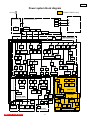
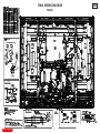
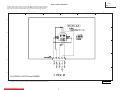
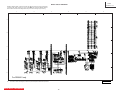
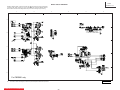
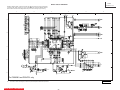
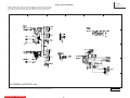
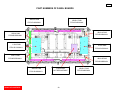
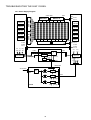
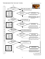
PA
No. 0226
P50X901 / DW3-D
P50V701 / DW3-D
P50S601 / DW3-F
SERVICE MANUAL
R/C: CLU-4372A
R/C: CLU-4374A
R/C: CLU-4373A
p/n HL02402
p/n HL02404
p/n HL02403
P50X901
P50V701
P50S601
SERVICE MANUAL REVISION HISTORY INFORMATION
DATE
REVISION #
REASON
Oct, 08, 2007
SM00001
FIRST ISSUE OF MANUAL
Nov, 12, 2007
CH1
Added Remote Control Info. How to enter Service Menu (Page 31)
Nov, 12, 2007
CH1
Added In-Depth 50AF1 Panel Troubleshooting Flowchart (Page 32)
Nov, 27, 2007
CH2
Added additional adjustment details about power supply (Page 48)
Dec, 05, 2007
CH3
Added note about power supply adjustment (Page 4)
SPECIFICATIONS AND PARTS ARE SUBJECT TO CHANGE FOR IMPROVEMENT
PLASMA DISPLAY PANEL
MAY 2007
HHEA-MANUFACTURING DIVISION
PA
No. 0226
P50X901 / DW3-D
P50V701 / DW3-D
P50S601 / DW3-F
SERVICE MANUAL
R/C: CLU-4372A
R/C: CLU-4374A
R/C: CLU-4373A
p/n HL02402
p/n HL02404
p/n HL02403
P50X901
P50V701
P50S601
This ADDENDUM is made due to the new models P50X901 (DW3D), P50V701 (DW3D) and P50S601 (DW3F).
They are different to models P50H401 (DW3A), P50T501 (DW3A) and P50H4011 (DW3A). The Main difference is the panel,
the X/V/S models use "AF1" Plasma Panel and the H/T Models use "AE1" Plasma Panel. Software (Digital Main PWB) is also
different because of Plasma Panel difference.
Refer to Service Manual PA0224 when servicing X/V/S models in regards to other adjustments not covered in this addendum.
This ADDENDUM indicates only the differences and special considerations to be taken when servicing the X/V/S models.
TO GO TO A CHAPTER, CLICK ON ITS HEADING BELOW
CONTENTS
SPECIFICATIONS ...................................................................................................
ADJUSTMENTS (See below for Power Supply Adjustment Info.) ...........................
BLOCK DIAGRAMS .................................................................................................
CONNECTOR DIAGRAMS ......................................................................................
FINAL WIRING DIAGRAM .......................................................................................
QUICK DISASSEMBLY GUIDE ...............................................................................
CIRCUIT SCHEMATIC DIAGRAMS ........................................................................
PARTS LIST ............................................................................................................
PANEL PARTS .......................................................................................................
PANEL CONNECTORS ..........................................................................................
REMOTE CONTROL “HOW TO ENTER SERVICE MENU” DW-1, 2 AND 3 .........
IN DEPTH 55 INCH PANEL (50AF1) TROUBLESHOOTING FLOW CHARTS ......
REPLACING THE POWER SUPPLY INFORMATION and ADJUSTMENTS .........
CAUTION:
2
4
5
7
9
11
13~27
28
29
30
31
32
48
These servicing instructions are for use by qualified service personnel only. To reduce the risk of
Electric shock do not perform any servicing other than that contained in the operating instructions
Unless you are qualified to do so. Before servicing this chassis, it is important that the service
Technician read the “IMPORTANT SAFETY INSTRUCTIONS” in this service manual.
SAFETY NOTICE
USE ISOLATION TRANSFORMER WHEN SERVICING
Components having special safety characteristics are identified by a ! on the schematics and on the parts list in this
Service Data and its supplements and bulletins. Before servicing the chassis, it is important that the service technician
Read and follow the “Important Safety Instructions” in this Service Manual.
SPECIFICATIONS AND PARTS ARE SUBJECT TO CHANGE FOR IMPROVEMENT
PLASMA DISPLAY PANEL
MAY 2007
HHEA-MANUFACTURING DIVISION
DW3
SPECIFICATIONS
APPEARANCE
Model name
P50X901
P50S601
P50V701
Series Name
Director's
UltraVision
UltraVision
Cabinet Design
High Gloss Black/Frame, High Gloss Black/Bezel, High Gloss Hidden/SP
High Gloss Black/Frame, Black/Bezel, High Gloss Hidden/SP
High Gloss Black/Frame, Black/Bezel, High Gloss Hidden/SP
SYSTEM
No.
Model name
VHF(ch)
1
2
3
P50X901
P50S601
P50V701
2~13
Channel coverage band
UHF(ch)
CATV(ch)
14~69
A-5~A-1, A~I,J~W,W+1~W+94
Reception system
NTSC
ATSC
64QAM/
(8VSB) 256QAM
X
X
X
X
X
X
X
X
X
STRUCTURAL DIMENSIONS
No.
Model name
WIDTH
[mm]
HEIGHT
[mm]
DEPTH
[mm]
WEIGHT
[kg]
1
P50X901
1250
885(817)
423(134)
50.9(44.8)
2
3
P50S601
P50V701
1241.4
1241.4
884(820.2)
884(820.2)
422.7(129)
422.7(129)
49.8(43.7)
49.9(43.8)
Note
Without table
top stand.
EXTERNAL TERMINALS AND JACKS
Model
name
P50X901
P50S601
P50V701
Model
name
P50X901
P50S601
P50V701
Rear
A/V
IN
3
3
3
Front
A/V
IN
1
1
1
S
IN
1
1
1
S
IN
-
-
-
COMP.
IN
2
2
2
COMP.
IN
-
-
-
TABLE OF CONTENTS
HDMI
2
2
2
HDMI
1
1
1
M
OUT
1
1
1
Photo
(SD)
1
1
1
A
OUT
1
1
1
Subwoofer
OUT
-
-
-
Upgrade
←Common
←Common
←Common
2
DV
IN
-
-
-
ANT
IN
1
1
1
Rear
IR OUT
1
-
1
OPT
OUT
1
1
1
IR OUT
/G-LINK
1
(1: Service)
1
DV IN
IEEE 1394
-
-
-
POD
CARD
1
-
1
SWIVEL
OUT
1
1
1
RS232C
1
1
1
DW3
MAIN FEATURES
No.
Feature
1
Panel
2
Resolution
3
4
5
6
7
8
9
10
11
12
13
14
15
16
17
18
19
20
21
Front Filter with ARF
(Transparency)
Seine2
FRC (FC8)
One NTSC/ATSC Tuner
POD (Point Of Deployment)
PinP (Digital/External Analog SPLIT)
3 Picture Mode
Color Temperature Mode
Color Decoding Adjustment
Color Management Adjustment
7 Mode Aspect Ratio Interchangeable
EPG (G-GUIDE) Function
SD-card Photo Viewer
Audio Output
Swivel
AV NET, AV NET Learning
IR Pass Through
OSD Design
Energy Star
P50
X901
AF1
1920x
1080i
Mesh
(36%)
X
X
X
X
X
X
4
X
X
X
X
X
10W x2
Power
X
X
Direc.
-
P50
S601
AF1
1920x
1080i
Mesh
(41%)
X
-
X
-
-
X
4
-
-
X
-
-
10W x2
Power
-
-
B
-
P50
V701
AF1
1920x
1080i
Mesh
(36%)
X
X
X
X
X
X
4
-
-
X
X
X
10W x2
Power
X
X
C
-
POWER CONSUMPTION
MODEL
NAME
P50X901
P50S601
P50V701
INDICATED
Max. Rating
605W
587W
605W
VALUE
Max. Rating
5.7A
5.3A
5.7A
(Average Rating)
364W
350W
364W
SAFETY KEY COMPONENTS
Symbol.No. / P/N / Spec.
F9A1 / P#FN00551 / Fuse
10A
TABLE OF CONTENTS
Model
P50X901, P50V701, P50S601
3
PST
Without POD
0.6W
0.6W
0.6W
[W]
CHASSIS
With POD
14W
14W
DW3D
DW3F
DW3D
DW3
ADJUSTMENTS
NOTE: The next adjustment procedure is only for the P50X901, P50V701 and the P50S601, refer to the service manual PA
no. 0224 for all the other adjustments.
POWER SUPPLY Vs, Va VOLTAGE ADJUSTMENT
Since Power Supply P#HA02202 is already adjusted by Manufacturer is not necessary to adjust any voltage.
Important Note: Please don’t move any control (potenciometer) on power supply since is already adjusted.
See Page 48: Please see page 48 for additional Power Supply Adjustment Information.
VIDEO COLOR TEMPERATURE ADJUSTMENT - BLACK AND WHITE MODE.
-Preparation
(1) Set the output of signal generator to white raster (Ratio: 100%).
(2) Component signal (480i)
Video level:
0.7Vp-p
SYNC:
0.3Vp-p
Set-up level:
0V
(3) Input white raster signal into COMPONENT input terminal.
(4) Set user control to Day (Dynamic) mode (Picture mode).
(5) Confirm that the mode is set as ‘Factory setting mode’.
(6) Aspect: 4:3 Expanded.
-Adjustment
(1)
(2)
(3)
(4)
Perform the following adjustment with the remote control.
Set the CRT color analyzer (CA-100) at the center of the panel.
Ensure that the adjustment parameters R/G/B DRIVE(B/W) are all set as FF.
After receiving the PC signal, reduce the value of two (or only one) of the RGB adjustment
parameters step down two (or one) among adjustment R/G/B DRIVE(B/W) and adjust the value
shown below.
Specification
Video Color temperature (B/W)
x = 0.335± 0.005
y = 0.343± 0.005
( Color temp? 5400K)
At least one of the data should be FF.
-Remarks
(1) Color temperature should be adjusted under the condition in which the screen is the brightest,
thus the initial value for adjustment is set at its maximum.
(2) Adjustment is made by reducing brightness only. Reduce the brightest color for adjustment.
(3) Video color temperature & Adjustment number are the same, but addresses in the memory are
different, thus there’s no problem.
(4) When this adjustment item is done through MMC slot, Sniffer Jig must be inserted after the set is
switched to Sniffer Mode. (the PC would have trouble if this sequence is not kept.)
TABLE OF CONTENTS
4
DW3
BLOCK DIAGRAM
For P50X901, P50V701 and P50S601.
Y SUS
Scan Driver
Scan Driver
X-SUS
P50X901, P50V701 only.
Address Driver
Driver Controller
PDP
Panel
Module
LOGIC
LVDS Receiver Signal Controller
Vcego
Vsago
AC
Inlet
RGB
(LVDS)
Power
Supply
Unit
Filter PWB
Fuse
Data Controller
Main
Power SW
CPUgo
PDPgo
FAN
FAN
FAN
FAN
FC8 PWB
FC8
DDR2
DC-DC
Conv.
Main-Digital PWB
AC-CLK
Power2
Sub
Micro
PLD
(Nereid)
DC-DC
Conv.
Demodulator
Power1
POD PWB
PLD
(Oberon)
Seine2
A-chip
Seine2
D-chip
Audio
DSP
DDR2
Audio
ADC
Audio
PWM
Digital
Audio
Amplifier
Audio
DAC
VCXO
PLL
Digital/
Analog
Tuner
Video
SW
Reg.
For FAN
Audio
SW
A/V
Pin Jack
POD
Card I/F
DC-DC
(POD-Vcc)
Terminal PWB
UEI
HDMI
IR-Blaster
Driver
RS-232C
Motor
Driver
OPT-Audio
Output
Remote
Control
IR
Receiver
LED
LED PWB
Key
SW
A/V
Pin Jack
HDMI
I/F
Control PWB
SD/MMC
Card I/F
SD PWB
Speaker R
Speaker L
Stand
TABLE OF CONTENTS
5
DW3
Power system block diagram
P50X901, P50V701 only.
AC120V
PDP Panel Module
Filter PWB
Power Supply Unit
Vs
Va
Vcc
+16V
AC
SW
+15V
+10.5V
+5.6V
STBY+5V
Main-Digital PWB
+3.3V
Reg.
+12V
Reg.
Bus
SW
+5V
Reg.
+3.3V
Reg.
Digital
Audio Amp.
+9V
Reg.
Audio
DSP
Audio
PWM
+1.3V
DC-DC
Audio
DAC
+2.5V
Reg.
+3.3V
Reg.
+3.3V
Reg.
Cable
Equalizer
Key
ROM
+30V
Reg.
+3.3V
Reg.
+1.0V
DC-DC
Seine2-D
DDR2
Bus
SW
+5V
Reg.
Demodulator
+5V
Reg.
+5V
Reg.
Tuner
OOB
AV-Control
+9V
Reg.
LPF
Buffer
+5V
Reg.
AGC
I2C
Level shift
+9V
Reg.
+3.3V
Reg.
+2.5V
Reg.
Vari.
Reg.
x2
FAN
x2
FAN
IR-Blaster
Driver
Swivel
Motor
Driver
Swivel
Stand
Vari.
Reg.
PODVcc
PODVpp
POD PWB
FC8 PWB
Oberon2
+1.8V
DC-DC
+1.05V
DC-DC
x2
IR-receiver
LED
I2C
Buffer
LED PWB
TABLE OF CONTENTS
Clock
Buffer
SD PWB
SD
MMC
+1.05V
Reg.
Buffer
Control PWB
6
FC8DDR2
PLD
(Nereid)
+3.3V
DC-DC
+1.2V
Reg.
Buffer
OPT
Output
Seine2-A
Flash Memory
(OneNand)
VCXO PLL
AV SW
+3.3V
Reg.
IR
Mod.
+2.5V
Reg.
+9V
Reg.
Terminal PWB
+1.5V
Reg.
+5V
Reg.
+3.0V
Reg.
+1.8V
Reg.
Sub
MICRO
+3.3V
Reg.
+2.5V
Reg.
Seine2-D
+5V
Reg.
+3.3V
DC-DC
+1.3V
Reg.
+3.3V
Reg.
Audio
ADC
+1.8V
DC-DC
x2
+3.3V
Reg.
FC8
+1.8V
Reg.
LVDS
SW
DW3
CONNECTIONS DIAGRAM
For P50S601.
Power Supply Unit
PDP Module
CONNECTION DIAGRAM
CN64
VH-10P
AC INLET
FILTER PWB
PFAC
VT-2P
AC IN
Va
N.C.
Vcc
GND
GND
GND
N.C.
Vs
Vs
Vs
PPU1
VT-2P
CN61
VT-2P
L
2 AC(L)
AC(L)
1
1 AC(L)
N
1 AC(N)
AC(N)
2
2 AC(N)
CN23
VH-10P
1
2
3
4
5
6
7
8
9
10
1
2
3
4
5
6
7
8
9
10
CN68
PH-9P
FG
Vcc
GND
N.C.
GND
Vra
Vrs
Vcego
Vsago
N.C.
Va
N.C.
Vcc
GND
GND
GND
N.C.
Vs
Vs
Vs
CN8
PH-9P
1
2
3
4
5
6
7
8
9
1
2
3
4
5
6
7
8
9
Vcc
GND
N.C.
GND
Vra
Vrs
Vcego
Vsago
N.C.
Main Digital board
CN63
EH-8P
STBY+5V
GND
N.C.
PoWERoFF
ACCLoCK
PoWER1
PoWER2
N.C.
PPM1
ZH-08H
1
2
3
4
5
6
7
8
1
2
3
4
5
6
7
8
CNPPS
EH-15P
+5.6V
+5.6V
+5.6V
GND
GND
GND
+10.5V
GND
+16V
GND
GND
GND
+15V
+15V
+15V
EC01
FI-RE51S
STBY+5V
GND
N.C.
PoWERoFF
ACCLoCK
PoWER1
PoWER2
PNLoN
GND
SDA
SCL
GND
PNL_RX
iRQ
PNL_TX
PDWN
PNLRST
PNLoN
GND
TA1TA1+
TB1TB1+
TC1TC1+
GND(LVDS)
TCLK1TCLK1+
GND
TD1TD1+
TE1TE1+
GND
GND
TA2TA2+
TB2TB2+
TC2TC2+
GND(LVDS)
TCLK2TCLK2+
GND
TD2TD2+
TE2TE2+
GND
GND
GND
GND
GND
N.C.
PNL_MoDE
PNL_P2
PNL_P0
PNL_CLK
PPM2
DF3D-15H
1
2
3
4
5
6
7
8
9
10
11
12
13
14
15
1
2
3
4
5
6
7
8
9
10
11
12
13
14
15
+5.6V
+5.6V
+5.6V
GND
GND
GND
+10.5V
GND
+16V
GND
GND
GND
N.C.
N.C.
N.C.
PPM3
PPM2
DF3D-15H
PA-6V
1
2
3
4
5
6
GND
GND
GND
+15V
+15V
+15V
TERMINAL PWB
PSM
501497-160VS
SWIVEL PWB
PWT
52418-05HS-D
1
3
5
7
9
11
13
15
17
19
21
23
25
27
29
31
33
35
37
39
41
43
45
47
49
51
53
55
57
59
61
63
65
67
69
71
73
75
77
79
81
83
85
87
89
91
93
95
97
99
101
103
105
107
109
111
113
115
117
119
121
123
125
127
129
131
133
135
137
139
141
143
145
147
149
151
153
155
157
159
PTW
53290-05VP-D
GND
MoToR+
MoToRJoiNTDET
SW_CoM
1
2
3
4
5
VCC
LoCK
GND
1
2
3
VCC
LoCK
GND
1
2
3
1
2
3
4
5
GND
MoToR+
MoToRJoiNTDET
SW_CoM
FAN
PFA1
ZH-03H
1 VCC
2 LoCK
3 GND
FAN
PFA2
ZH-03H
1 VCC
2 LoCK
3 GND
FAN
PFB1
ZH-04H
VCC
LoCK
GND
1
2
3
VCC
LoCK
GND
1
2
3
1
2
3
4
VCC
LoCK
GND
N.C.
FAN
PFB2
ZH-04H
1
2
3
4
VCC
LoCK
GND
N.C.
GND
+5.6V
+5.6V
+5.6V
+5.6V
GND
SBY+5.0V
GND
+16V
GND
N.C.
iRoUT
N.C.
N.C.
FiN
RiN
CPDET
SWVLDET
GND
AEP_R
AEP_L
GND
ASP_R
ASP_L
GND
N.C.
GND
SEL_L_S
SEL_R_S
GND
SCL1_3V_100
SDA1_3V_100
GND
SCL_TU
SDA_TU
ANA/DIGI
GND
IF_AGC
GND
FDC_AGC
GND
FAT_INP
GND
GND
FAT_INN
GND
FDC_INP
GND
FDC_INN
GND
FS_OUTP
GND
PoWERoFF
GND
FS_OUTN
GND
GND
FAN_DET
GND
MTV_AFC
SIG_DET
N.C.
PNLoN
GND
REC_MUTE
GND
N.C.
N.C.
GND
N.C.
N.C.
N.C.
N.C.
N.C.
N.C.
N.C.
N.C.
GND
N.C.
GND
PMS1
501493-160VP
GND
D+3.3V
D+3.3V
D+3.3V
GND
GND
SBY+3.3V
GND
+10V
SWiVEL_G
MAiN_Y/V
GND
MAiN_Y_E
GND
MAiN_PB
GND
MAiN_PR/C
GND
SUB_Y/V
GND
S/PDiT
GND
SD_Yo
GND
SD_Co
GND
FAN_EN
N.C.
GND
N.C.
N.C.
GND
N.C.
N.C.
GND
SEL_L_M
SEL_R_M
GND
UATXD3
UARXD3
GND
SDA2_3V_100
GND
SCL2_3V_100
GND
N.C.
N.C.
PoWER_2_Td
N.C.
GND
FAN_CONT
N.C.
GND
N.C.
N.C.
N.C.
N.C.
GND
N.C.
GND
N.C.
GND
N.C.
GND
N.C.
GND
N.C.
GND
AVCTXD
AVCRXD
AVCCTS_N
AVCRTS_N
GND
N.C.
N.C.
N.C.
N.C.
N.C.
N.C.
N.C.
2
4
6
8
10
12
14
16
18
20
22
24
26
28
30
32
34
36
38
40
42
44
46
48
50
52
54
56
58
60
62
64
66
68
70
72
74
76
78
80
82
84
86
88
90
92
94
96
98
100
102
104
106
108
110
112
114
116
118
120
122
124
126
128
130
132
134
136
138
140
142
144
146
148
150
152
154
156
158
160
V4_CY
GND
V4_Y
GND
V4_C
GND
V4_L
V4_R
GND
T+9V
PWRKEY
ADKEY0
ADKEY1
GND
1
2
3
4
5
6
7
8
9
10
V4_CY
GND
V4_Y
GND
V4_C
GND
V4_L
V4_R
GND
T+9V
+
-
Lout-P
Lout-N
Rout-P
Rout-N
SD PWB
PSD
PDS
CNPPS
501331-12V
EH-15P
501568-12H
SDCLK
SDCMD
GND
SDDAT0
SDDAT1
SDDAT2
SDDAT3
+5.6V
SDCD
SDWP
GND
D+3.3V
VBUS
VBUS
VBUS
GND
D+
DGND
+3.3V
+5V
WP
HPD
DDCPOW
GND
SDA
SCL
ACK
GND
ClockClock+
GND
Data0Data0+
GND
Data1Data1+
GND
Data2Data2+
GND
CEC
GND
PSC
PTF
ZH-13H
GH-04H
1 PWRKEY
2 ADKEY0
3 ADKEY1
4 GND
1
2
3
4
5
6
7
8
9
10
11
Speaker (R)
+
-
LED PWB
TABLE OF CONTENTS
1
2
3
4
PDS
PSD
PPM2
501568-12H
DF3D-15H
501331-12V
1
2
3
4
5
6
7
8
9
10
11
12
P403
PH01
FIR-31V
FI-RE31S
PLS
501331-11V
iR_iN
STBY+3.3V
iR_CAPiN
GND
+5.6V
STBY+5V
ALARMLED0
PWRLED0
PWRLED1
MLEDG_N
MLEDR_N
GND
SDA
SCL
N.C.
N.C.
IRQOUT
N.C.
PDWN
CPUGO
PDPGO
GND
RA0RA0+
RA1RA1+
RA2RA2+
GND
RACLKRACLK+
GND
RA3RA3+
RA4RA4+
GND
GND
RB0RB0+
RB1RB1+
RB2RB2+
GND
RBCLKRBCLK+
GND
RB3RB3+
RB4RB4+
GND
GND
GND
GND
GND
N.C.
N.C.
N.C.
N.C.
N.C.
PSPK
PA-04V
PTC
PTF
ZH-13H
GH-10V
1
2
3
4
5
6
7
8
9
10
11
12
13
14
1
2
3
4
5
6
7
8
9
10
11
12
13
14
15
16
17
18
19
20
21
22
23
24
25
26
27
28
29
30
31
32
33
34
35
36
37
38
39
40
41
42
43
44
45
46
47
48
49
50
51
Speaker (L)
CONTROL PWB
PCST
GH-14V
CN1
FI-RE51S
51
50
49
48
47
46
45
44
43
42
41
40
39
38
37
36
35
34
33
32
31
30
29
28
27
26
25
24
23
22
21
20
19
18
17
16
15
14
13
12
11
10
9
8
7
6
5
4
3
2
1
PSL
PA01
501786-8011
501568-11H
1 iR_iN
2 STBY+3.3V
3 iR_CAPiN
4 GND
5 +5.6V
6 STBY+5V
7 ALARMLED0
8 PWRLED0
9 PWRLED1
10 MLEDG_N
11 MLEDR_N
7
1
2
3
4
5
6
7
8
9
10
11
12
SDCLK
SDCMD
GND
SDDAT0
SDDAT1
SDDAT2
SDDAT3
+5.6V
SDCD
SDWP
GND
D+3.3V
PH01
P403
FIR-31H
FI-RE31S
31
30
29
28
27
26
25
24
23
22
21
20
19
18
17
16
15
14
13
12
11
10
9
8
7
6
5
4
3
2
1
1
2
3
4
5
6
7
8
9
10
11
12
13
14
15
16
17
18
19
20
21
22
23
24
25
26
27
28
29
30
31
VBUS
VBUS
VBUS
GND
D+
DGND
+3.3V
+5V
WP
HPD
DDCPOW
GND
SDA
SCL
ACK
GND
ClockClock+
GND
Data0Data0+
GND
Data1Data1+
GND
Data2Data2+
GND
CEC
GND
DW3
CONNECTIONS DIAGRAM
For P50V701 and P50X901
Power Supply Unit
PDP Module
CONNECTION DIAGRAM
CN64
VH-10P
AC INLET
FILTER PWB
PFAC
VT-2P
AC IN
Va
N.C.
Vcc
GND
GND
GND
N.C.
Vs
Vs
Vs
PPU1
VT-2P
CN61
VT-2P
L
2 AC(L)
AC(L)
1
1 AC(L)
N
1 AC(N)
AC(N)
2
2 AC(N)
CN23
VH-10P
1
2
3
4
5
6
7
8
9
10
1
2
3
4
5
6
7
8
9
10
CN68
PH-9P
FG
Vcc
GND
N.C.
GND
Vra
Vrs
Vcego
Vsago
N.C.
Va
N.C.
Vcc
GND
GND
GND
N.C.
Vs
Vs
Vs
CN8
PH-9P
1
2
3
4
5
6
7
8
9
1
2
3
4
5
6
7
8
9
Vcc
GND
N.C.
GND
Vra
Vrs
Vcego
Vsago
N.C.
Main Digital board
CN63
EH-8P
STBY+5V
GND
N.C.
PoWERoFF
ACCLoCK
PoWER1
PoWER2
N.C.
PPM1
ZH-08H
1
2
3
4
5
6
7
8
CNPPS
EH-15P
+5.6V
+5.6V
+5.6V
GND
GND
GND
+10.5V
GND
+16V
GND
GND
GND
+15V
+15V
+15V
1
2
3
4
5
6
7
8
EC01
FI-RE51S
STBY+5V
GND
N.C.
PoWERoFF
ACCLoCK
PoWER1
PoWER2
PNLoN
GND
SDA
SCL
GND
PNL_RX
iRQ
PNL_TX
PDWN
PNLRST
PNLoN
GND
TA1TA1+
TB1TB1+
TC1TC1+
GND(LVDS)
TCLK1TCLK1+
GND
TD1TD1+
TE1TE1+
GND
GND
TA2TA2+
TB2TB2+
TC2TC2+
GND(LVDS)
TCLK2TCLK2+
GND
TD2TD2+
TE2TE2+
GND
GND
GND
GND
GND
N.C.
PNL_MoDE
PNL_P2
PNL_P0
PNL_CLK
PPM2
DF3D-15H
1
2
3
4
5
6
7
8
9
10
11
12
13
14
15
1
2
3
4
5
6
7
8
9
10
11
12
13
14
15
+5.6V
+5.6V
+5.6V
GND
GND
GND
+10.5V
GND
+16V
GND
GND
GND
N.C.
N.C.
N.C.
PPM3
PPM2
DF3D-15H
PA-6V
1
2
3
4
5
6
GND
GND
GND
+15V
+15V
+15V
TERMINAL PWB
PSM
501497-160VS
SWIVEL PWB
PWT
52418-05HS-D
1 GND
3 +5.6V
5 +5.6V
7 +5.6V
9 +5.6V
11 GND
13 SBY+5.0V
15 GND
17 +16V
19 GND
21 N.C.
23 iRoUT
25 N.C.
27 N.C.
29 FiN
31 RiN
33 CPDET
35 SWVLDET
37 GND
39 AEP_R
41 AEP_L
43 GND
45 ASP_R
47 ASP_L
49 GND
51 N.C.
53 GND
55 SEL_L_S
57 SEL_R_S
59 GND
61 SCL1_3V_100
63 SDA1_3V_100
65 GND
67 SCL_TU
69 SDA_TU
71 ANA/DIGI
73 GND
75 IF_AGC
77 GND
79 FDC_AGC
81 GND
83 FAT_INP
85 GND
87 GND
89 FAT_INN
91 GND
93 FDC_INP
95 GND
97 FDC_INN
99 GND
101 FS_OUTP
103 GND
105 PoWERoFF
107 GND
109 FS_OUTN
111 GND
113 GND
115 FAN_DET
117 GND
119 MTV_AFC
121 SIG_DET
123 N.C.
125 PNLoN
127 GND
129 REC_MUTE
131 GND
133 N.C.
135 N.C.
137 GND
139 N.C.
141 N.C.
143 N.C.
145 N.C.
147 N.C.
149 N.C.
151 N.C.
153 N.C.
155 GND
157 N.C.
159 GND
PTW
53290-05VP-D
GND
MoToR+
MoToRJoiNTDET
SW_CoM
1
2
3
4
5
VCC
LoCK
GND
1
2
3
VCC
LoCK
GND
1
2
3
1
2
3
4
5
GND
MoToR+
MoToRJoiNTDET
SW_CoM
FAN
PFA1
ZH-03H
1 VCC
2 LoCK
3 GND
FAN
PFA2
ZH-03H
1 VCC
2 LoCK
3 GND
FAN
PFB1
ZH-04H
VCC
LoCK
GND
1
2
3
VCC
LoCK
GND
1
2
3
1
2
3
4
VCC
LoCK
GND
N.C.
FAN
PFB2
ZH-04H
1 VCC
2 LoCK
3 GND
4 N.C.
PMS1
501493-160VP
GND
D+3.3V
D+3.3V
D+3.3V
GND
GND
SBY+3.3V
GND
+10V
SWiVEL_G
MAiN_Y/V
GND
MAiN_Y_E
GND
MAiN_PB
GND
MAiN_PR/C
GND
SUB_Y/V
GND
S/PDiT
GND
SD_Yo
GND
SD_Co
GND
FAN_EN
N.C.
GND
N.C.
N.C.
GND
N.C.
N.C.
GND
SEL_L_M
SEL_R_M
GND
UATXD3
UARXD3
GND
SDA2_3V_100
GND
SCL2_3V_100
GND
N.C.
N.C.
PoWER_2_Td
N.C.
GND
FAN_CONT
N.C.
GND
N.C.
N.C.
N.C.
N.C.
GND
N.C.
GND
N.C.
GND
N.C.
GND
N.C.
GND
N.C.
GND
AVCTXD
AVCRXD
AVCCTS_N
AVCRTS_N
GND
N.C.
N.C.
N.C.
N.C.
N.C.
N.C.
N.C.
2
4
6
8
10
12
14
16
18
20
22
24
26
28
30
32
34
36
38
40
42
44
46
48
50
52
54
56
58
60
62
64
66
68
70
72
74
76
78
80
82
84
86
88
90
92
94
96
98
100
102
104
106
108
110
112
114
116
118
120
122
124
126
128
130
132
134
136
138
140
142
144
146
148
150
152
154
156
158
160
V4_CY
GND
V4_Y
GND
V4_C
GND
V4_L
V4_R
GND
T+9V
PWRKEY
ADKEY0
ADKEY1
GND
1
2
3
4
5
6
7
8
9
10
V4_CY
GND
V4_Y
GND
V4_C
GND
V4_L
V4_R
GND
T+9V
+
-
Lout-P
Lout-N
Rout-P
Rout-N
1
2
3
4
Speaker (R)
+
-
SD PWB
PSD
PDS
CNPPS
501331-12V
EH-15P
501568-12H
SDCLK
SDCMD
GND
SDDAT0
SDDAT1
SDDAT2
SDDAT3
+5.6V
SDCD
SDWP
GND
D+3.3V
PDS
PSD
PPM2
501568-12H
DF3D-15H
501331-12V
1
2
3
4
5
6
7
8
9
10
11
12
1
2
3
4
5
6
7
8
9
10
11
12
P403
PH01
FIR-31V
FI-RE31S
VBUS
VBUS
VBUS
GND
D+
DGND
+3.3V
+5V
WP
HPD
DDCPOW
GND
SDA
SCL
ACK
GND
ClockClock+
GND
Data0Data0+
GND
Data1Data1+
GND
Data2Data2+
GND
CEC
GND
PSC
PTF
ZH-13H
GH-04H
1
2
3
4
PWRKEY
ADKEY0
ADKEY1
GND
LED PWB
PLS
501331-11V
iR_iN
STBY+3.3V
iR_CAPiN
GND
+5.6V
STBY+5V
ALARMLED0
PWRLED0
PWRLED1
MLEDG_N
MLEDR_N
PSL
PA01
501786-8011
501568-11H
1
2
3
4
5
6
7
8
9
10
11
1
2
3
4
5
6
7
8
9
10
11
iR_iN
STBY+3.3V
iR_CAPiN
GND
+5.6V
STBY+5V
ALARMLED0
PWRLED0
PWRLED1
MLEDG_N
MLEDR_N
SDCLK
SDCMD
GND
SDDAT0
SDDAT1
SDDAT2
SDDAT3
+5.6V
SDCD
SDWP
GND
D+3.3V
PH01
P403
FIR-31H
FI-RE31S
31
30
29
28
27
26
25
24
23
22
21
20
19
18
17
16
15
14
13
12
11
10
9
8
7
6
5
4
3
2
1
1
2
3
4
5
6
7
8
9
10
11
12
13
14
15
16
17
18
19
20
21
22
23
24
25
26
27
28
29
30
31
POD PWB
VBUS
VBUS
VBUS
GND
D+
DGND
+3.3V
+5V
WP
HPD
DDCPOW
GND
SDA
SCL
ACK
GND
ClockClock+
GND
Data0Data0+
GND
Data1Data1+
GND
Data2Data2+
GND
CEC
GND
FC8 PWB
PW01
501864-8090
D+3.3V
SBADD13
SBADD12
SBADD11
SBADD10
SBADD9
GND
SBADD8
SBADD7
SBADD6
SBADD5
SBADD4
SBADD3
SBADD2
SBADD1
GND
SBDAT7
SBDAT6
SBDAT5
SBDAT4
SBDAT3
SBDAT2
SBDAT1
SBDAT0
SBoE_N
SBWE_N
SBBE0_N
SBACK_N
GND
SBCLK_3
RESET1_N
CoNF_PRoG
CoNF_iNiT
CoNF_DoNE
GND
MCLKo
GND
MDoD
MoVAL
MoSTRT
CRXiN
DRXiN
GND
MPEG_PCLK
GND
MPEG_PD7
MPEG_PD6
MPEG_PD5
MPEG_PD4
MPEG_PD3
MPEG_PD2
MPEG_PD1
MPEG_PD0
MPEG_PEN
MPEG_PSYNC
GND
PLL_66M
GND
SBCE6a_N
SBCE7_N
PoD_CD_N
iREQ_N
PG_+5.6V
PNLoN
SDDAT3
SDDAT2
SDDAT1
SDWP
SDDAT0
SDCD
SDCMD
GND
SDCLK
GND
+5.6V
+5.6V
+5.6V
+5.6V
+5.6V
TABLE OF CONTENTS
GND
SDA
SCL
N.C.
N.C.
IRQOUT
N.C.
PDWN
CPUGO
PDPGO
GND
RA0RA0+
RA1RA1+
RA2RA2+
GND
RACLKRACLK+
GND
RA3RA3+
RA4RA4+
GND
GND
RB0RB0+
RB1RB1+
RB2RB2+
GND
RBCLKRBCLK+
GND
RB3RB3+
RB4RB4+
GND
GND
GND
GND
GND
N.C.
N.C.
N.C.
N.C.
N.C.
PSPK
PA-04V
PTC
PTF
ZH-13H
GH-10V
1
2
3
4
5
6
7
8
9
10
11
12
13
14
1
2
3
4
5
6
7
8
9
10
11
12
13
14
15
16
17
18
19
20
21
22
23
24
25
26
27
28
29
30
31
32
33
34
35
36
37
38
39
40
41
42
43
44
45
46
47
48
49
50
51
Speaker (L)
CONTROL PWB
PCST
GH-14V
CN1
FI-RE51S
51
50
49
48
47
46
45
44
43
42
41
40
39
38
37
36
35
34
33
32
31
30
29
28
27
26
25
24
23
22
21
20
19
18
17
16
15
14
13
12
11
10
9
8
7
6
5
4
3
2
1
PA01
501786-8090
80
79
78
77
76
75
74
73
72
71
70
69
68
67
66
65
64
63
62
61
60
59
58
57
56
55
54
53
52
51
50
49
48
47
46
45
44
43
42
41
40
39
38
37
36
35
34
33
32
31
30
29
28
27
26
25
24
23
22
21
20
19
18
17
16
15
14
13
12
11
10
9
8
7
6
5
4
3
2
1
1
2
3
4
5
6
7
8
9
10
11
12
13
14
15
16
17
18
19
20
21
22
23
24
25
26
27
28
29
30
31
32
33
34
35
36
37
38
39
40
41
42
43
44
45
46
47
48
49
50
51
52
53
54
55
56
57
58
59
60
61
62
63
64
65
66
67
68
69
70
71
72
73
74
75
76
77
78
79
80
PMF1
501497-160VS
D+3.3V
SBADD13
SBADD12
SBADD11
SBADD10
SBADD9
PoD_Ari
SBADD8
SBADD7
SBADD6
SBADD5
SBADD4
SBADD3
SBADD2
SBADD1
GND
SBDAT7
SBDAT6
SBDAT5
SBDAT4
SBDAT3
SBDAT2
SBDAT1
SBDAT0
SBoE11_N
SBWE11_N
SBBE0_N
SBACK_N
GND
SBCLK_3
RESET1_N
CoNF_PRoG
CoNF_iNiT
CoNF_DoNE
GND
MCLKo
GND
MDoD
MoVAL
MoSTRT
CRXiN
DRXiN
GND
PoD_PCLK
GND
MPEG_PD7
MPEG_PD6
MPEG_PD5
MPEG_PD4
MPEG_PD3
MPEG_PD2
MPEG_PD1
PoD_PD0
PoD_PEN
PoD_PSYNC
GND
PLL_66M
GND
SBCE6a_N
SBCE7_N
PoD_CD_N
iREQ_N
PG_+5.6V
PNLoN
SDDAT3
SDDAT2
SDDAT1
SDWP
SDDAT0
SDCD
SDCMD
GND
SDCLK
GND
1
3
5
7
9
11
13
15
17
19
21
23
25
27
29
31
33
35
37
39
41
43
45
47
49
51
53
55
57
59
61
63
65
67
69
71
73
75
77
79
81
83
85
87
89
91
93
95
97
99
101
103
105
107
109
111
113
115
117
119
121
123
125
127
129
131
133
135
137
139
141
143
145
147
149
151
153
155
157
159
+5.6V
+5.6V
+5.6V
+5.6V
+5.6V
8
GND
+5.6V
+5.6V
+5.6V
+5.6V
+5.6V
GND
D+3.3V
GND
GND
GND
GND
RA1RA1+
GND
RB1RB1+
GND
RC1RC1+
GND
RCLK1RCLK1+
GND
RD1RD1+
GND
RE1RE1+
GND
RA2RA2+
GND
RB2RB2+
GND
RC2RC2+
GND
RCLK2RCLK2+
GND
RD2RD2+
GND
RE2RE2+
GND
GND
SBCLK_2
GND
SBCE6c_N
SBWE_N
SBoE_N
SBDAT0
SBDAT1
SBDAT2
SBDAT3
SBDAT4
SBDAT5
SBDAT6
SBDAT7
RESET2_N
FCoNT
FPHASE
PC_SEL
PC_RST
GND
PLL_27M_FC8
GND
TELEROCK
AUDiooUT
LRCKoUT
BiToUT
MoDE0
FRC0
FRC2
FRC4
FRC6
FRC8
P602
501493-160VP
GND
+5.6V
+5.6V
+5.6V
+5.6V
+5.6V
GND
D+3.3V
GND
GND
GND
GND
TA1TA1+
GND
TB1TB1+
GND
TC1TC1+
GND
TCLK1TCLK1+
GND
TD1TD1+
GND
TE1TE1+
GND
TA2TA2+
GND
TB2TB2+
GND
TC2TC2+
GND
TCLK2TCLK2+
GND
TD2TD2+
GND
TE2TE2+
GND
CPUSEL
SBADD1
SBADD2
SBADD3
SBADD4
SBADD5
SBADD6
SBADD7
SBADD8
SBADD9
SBADD10
SBADD11
SBADD12
SBADD13
EXTLD
PBLK
GND
SCL1_3V_100
SDA1_3V_100
GND
PoWER_2_Td
GND
VSYNC
AUDioiN
LRCKiN
BiTiN
MODE1
FRC1
FRC3
FRC5
FRC7
FRC9
2
4
6
8
10
12
14
16
18
20
22
24
26
28
30
32
34
36
38
40
42
44
46
48
50
52
54
56
58
60
62
64
66
68
70
72
74
76
78
80
82
84
86
88
90
92
94
96
98
100
102
104
106
108
110
112
114
116
118
120
122
124
126
128
130
132
134
136
138
140
142
144
146
148
150
152
154
156
158
160
FINAL WIRING DIAGRAM
FOR P50V701 AND P50S601
TABLE OF CONTENTS
9
DW3
FINAL WIRING DIAGRAM
P50X901
TABLE OF CONTENTS
10
DW3
DW3D, DW3F
QUICK DISASSEMBLE GUIDE(These two pages show diffrential points from H/T Models, other pages are common)
POWER UNIT, FAN ASSY(P50S601, P50V701, P50X901)
① Remove Screw M3M 3*8 P#MJ03598( 4 pcs.)
Screw M3E 3*8 P#MJ03963( 2 pcs.)
⑥ Remove Screw M3D 4*10 P#MJ03895( 2 pcs.)
Screw M3D 4*10 P#MJ04067( 2 pcs.)
Panel fan Ass'y
② Remove Power Unit P#HA02202
⑦ Remove Screw M3D 4*10 P#MJ04067( 2 pcs.)
③ Remove Screw M3M 3*8 P#MJ03598( 3 pcs.)
Power Fan Ass'y
⑧ Remove Fan P#GS00697( 2 pcs.)
④ Remove Screw M3D 4*10 P#MJ03895( 2 pcs.)
⑤ Remove Fan P#GS00696( 2 pcs.)
PANEL FAN ASS'Y
SUPPORT
PANEL FAN ASS'Y DETAIL
METAL
METAL COVER
CUSHION
SUPPORT METAL
POWER FAN ASS'Y
POWER FAN ASS'Y DETAIL
FERRITE
CORE ASS'Y
SUPPORT METAL
METAL COVER
TABLE OF CONTENTS
11
DW3D
CHASSIS ASS'Y 2(P50V701, P50X901 ONLY)
① Remove Screw M3E 3*8 P#MJ03467( 2 pcs.)
② Remove Screw M3E 3*8 P#MJ03963( 2 pcs.)
③ Remove POD PWB ASS'Y P#JP55141
④ Remove Screw M3E 3*8 P#MJ03467( 2 pcs.)
⑤ Remove FC8 PWB ASS'Y P#JP56845
TABLE OF CONTENTS
12
DW3U
BASIC CIRCUIT DIAGRAM
1
2
3
NOTES 1 of 1
4
5
6
A
NOTES ABOUT THE SCHEMATICS.
B
C
D
The schematic drawings included in this service manual addendum are:
1. Swivel board
2. Filter board
3. Terminal board
4. LED board for P50X901 and for P50V701
5. POD board for P50X901 and for P50V701
Refer to the service manual PA no. 0224 for the next additional schematic drawings:
1. Control board (for P50X901, P50V701 and P50S601)
2. SD board (for P50X901, P50V701 and P50S601)
4. LED board for P50S601
E
NOTES
TABLE OF CONTENTS
13
PRODUCT SAFETY NOTE: Components marked with a ! and shaded have special characteristics
important to safety. Before replacing any of these components, read carefully the PRODUCT SAFETY
NOTE of this Service Manual. Don't degrade the safety of the receiver through improper servicing.
1
2
DW3U
BASIC CIRCUIT DIAGRAM
3
SWIVEL 1 of 1
4
5
6
A
B
C
D
E
For P50X901, P50V701 and P50S601
•
SWIVEL
Since this is a basic circuit diagram, the value of the parts is subject to be altered for improvement.
NOTES ABOUT THE SCHEMATICS
14
PRODUCT SAFETY NOTE: Components marked with a ! and shaded have special characteristics
important to safety. Before replacing any of these components, read carefully the PRODUCT SAFETY
NOTE of this Service Manual. Don't degrade the safety of the receiver through improper servicing.
1
2
DW3U
BASIC CIRCUIT DIAGRAM
3
FILTER 1 of 1
4
5
6
A
B
C
D
E
For P50X901, P50V701 and P50S601.
•
FILTER
Since this is a basic circuit diagram, the value of the parts is subject to be altered for improvement.
NOTES ABOUT THE SCHEMATICS
15
PRODUCT SAFETY NOTE: Components marked with a ! and shaded have special characteristics
important to safety. Before replacing any of these components, read carefully the PRODUCT SAFETY
NOTE of this Service Manual. Don't degrade the safety of the receiver through improper servicing.
1
2
DW3U
BASIC CIRCUIT DIAGRAM
3
TERMINAL 1 of 5
4
5
6
A
B
C
D
E
For P50S601 only
•
TERMINAL
Since this is a basic circuit diagram, the value of the parts is subject to be altered for improvement.
NOTES ABOUT THE SCHEMATICS
16
PRODUCT SAFETY NOTE: Components marked with a ! and shaded have special characteristics
important to safety. Before replacing any of these components, read carefully the PRODUCT SAFETY
NOTE of this Service Manual. Don't degrade the safety of the receiver through improper servicing.
1
2
DW3U
BASIC CIRCUIT DIAGRAM
3
TERMINAL 2 of 5
4
5
6
A
B
C
D
E
For P50S601 only
•
TERMINAL
Since this is a basic circuit diagram, the value of the parts is subject to be altered for improvement.
NOTES ABOUT THE SCHEMATICS
17
PRODUCT SAFETY NOTE: Components marked with a ! and shaded have special characteristics
important to safety. Before replacing any of these components, read carefully the PRODUCT SAFETY
NOTE of this Service Manual. Don't degrade the safety of the receiver through improper servicing.
1
2
DW3U
BASIC CIRCUIT DIAGRAM
3
TERMINAL 3 of 5
4
5
6
A
B
C
D
E
For P50S601 only
•
TERMINAL
Since this is a basic circuit diagram, the value of the parts is subject to be altered for improvement.
NOTES ABOUT THE SCHEMATICS
18
PRODUCT SAFETY NOTE: Components marked with a ! and shaded have special characteristics
important to safety. Before replacing any of these components, read carefully the PRODUCT SAFETY
NOTE of this Service Manual. Don't degrade the safety of the receiver through improper servicing.
1
2
DW3U
BASIC CIRCUIT DIAGRAM
3
TERMINAL 4 of 5
4
5
6
A
B
C
D
E
For P50S601 only
•
TERMINAL
Since this is a basic circuit diagram, the value of the parts is subject to be altered for improvement.
NOTES ABOUT THE SCHEMATICS
19
PRODUCT SAFETY NOTE: Components marked with a ! and shaded have special characteristics
important to safety. Before replacing any of these components, read carefully the PRODUCT SAFETY
NOTE of this Service Manual. Don't degrade the safety of the receiver through improper servicing.
1
2
DW3U
BASIC CIRCUIT DIAGRAM
3
TERMINAL 5 of 5
4
5
6
A
B
C
D
E
For P50S601 only
•
TERMINAL
Since this is a basic circuit diagram, the value of the parts is subject to be altered for improvement.
NOTES ABOUT THE SCHEMATICS
20
PRODUCT SAFETY NOTE: Components marked with a ! and shaded have special characteristics
important to safety. Before replacing any of these components, read carefully the PRODUCT SAFETY
NOTE of this Service Manual. Don't degrade the safety of the receiver through improper servicing.
1
2
DW3U
BASIC CIRCUIT DIAGRAM
3
TERMINAL 1 of 5
4
5
6
A
B
C
D
E
For P50X901 and P50V701 only
•
TERMINAL
Since this is a basic circuit diagram, the value of the parts is subject to be altered for improvement.
NOTES ABOUT THE SCHEMATICS
21
PRODUCT SAFETY NOTE: Components marked with a ! and shaded have special characteristics
important to safety. Before replacing any of these components, read carefully the PRODUCT SAFETY
NOTE of this Service Manual. Don't degrade the safety of the receiver through improper servicing.
1
2
DW3U
BASIC CIRCUIT DIAGRAM
3
TERMINAL 2 of 5
4
5
6
A
B
C
D
E
For P50X901 and P50V701 only
•
TERMINAL
Since this is a basic circuit diagram, the value of the parts is subject to be altered for improvement.
NOTES ABOUT THE SCHEMATICS
22
PRODUCT SAFETY NOTE: Components marked with a ! and shaded have special characteristics
important to safety. Before replacing any of these components, read carefully the PRODUCT SAFETY
NOTE of this Service Manual. Don't degrade the safety of the receiver through improper servicing.
1
2
DW3U
BASIC CIRCUIT DIAGRAM
3
TERMINAL 3 of 5
4
5
6
A
B
C
D
E
For P50X901 and P50V701 only
•
TERMINAL
Since this is a basic circuit diagram, the value of the parts is subject to be altered for improvement.
NOTES ABOUT THE SCHEMATICS
23
PRODUCT SAFETY NOTE: Components marked with a ! and shaded have special characteristics
important to safety. Before replacing any of these components, read carefully the PRODUCT SAFETY
NOTE of this Service Manual. Don't degrade the safety of the receiver through improper servicing.
1
2
DW3U
BASIC CIRCUIT DIAGRAM
3
TERMINAL 4 of 5
4
5
6
A
B
C
D
E
For P50X901 and P50V701 only
•
TERMINAL
Since this is a basic circuit diagram, the value of the parts is subject to be altered for improvement.
NOTES ABOUT THE SCHEMATICS
24
PRODUCT SAFETY NOTE: Components marked with a ! and shaded have special characteristics
important to safety. Before replacing any of these components, read carefully the PRODUCT SAFETY
NOTE of this Service Manual. Don't degrade the safety of the receiver through improper servicing.
1
2
DW3U
BASIC CIRCUIT DIAGRAM
3
TERMINAL 5 of 5
4
5
6
A
B
C
D
E
For P50X901 and P50V701 only
•
TERMINAL
Since this is a basic circuit diagram, the value of the parts is subject to be altered for improvement.
NOTES ABOUT THE SCHEMATICS
25
PRODUCT SAFETY NOTE: Components marked with a ! and shaded have special characteristics
important to safety. Before replacing any of these components, read carefully the PRODUCT SAFETY
NOTE of this Service Manual. Don't degrade the safety of the receiver through improper servicing.
1
2
DW3U
BASIC CIRCUIT DIAGRAM
3
LED 1 of 1
4
5
6
A
B
C
D
E
For P50X901 and P50V701 only. Refer to PA no. 0224 for the P50S601.
•
LED
Since this is a basic circuit diagram, the value of the parts is subject to be altered for improvement.
NOTES ABOUT THE SCHEMATICS
26
PRODUCT SAFETY NOTE: Components marked with a ! and shaded have special characteristics
important to safety. Before replacing any of these components, read carefully the PRODUCT SAFETY
NOTE of this Service Manual. Don't degrade the safety of the receiver through improper servicing.
1
2
DW3U
BASIC CIRCUIT DIAGRAM
3
POD 1 of 1
4
5
6
A
B
C
D
E
For P50X901 and P50V701 only
•
POD
Since this is a basic circuit diagram, the value of the parts is subject to be altered for improvement.
NOTES ABOUT THE SCHEMATICS
27
P50S601 / P50V701 / P50X901
Parts List
P50S601
DD00941
EK01933
EV01841
EW08433
FPF38R-XBD54621
FPF38R-XBU54611
FPF38RADM019F03
FPF41R-ABA56061
FPF41R-ABB56071
FPF41R-ABC56081
FPF41R-CBL02381
FPF41R-CBL02382
FPF41R-CBL02383
FPF41R-CBL02384
FPF41R-CBL02385
FPF41R-CBL02386
FPF41R-CBL27301
FPF41R-CBL27311
FPF41R-CBL27312
FPF41R-CBL27313
Not Replaceable
FPF41R-XSS56421
FPF41R-YSS56431
GK01652
GS00696
GS00697
HA02202
HL02403
JP55124
JP55134
UX28027
KS22255
PC07042
PC07071
PH40153
PH41211
PH41771
PH41772
PH41781
PH43353
PH43572
PH43771
PH43772
PU00961
QA03713
QD56864
QJ03754
QR71591
UE27036
FPF50C240135UA-55
WIRE (PROCESSED) JF04R0R021970
POWER CORD 125V10A UL/CSA
8P PLUG CODE L=350MM
XBUS (D)
XBUS (U)
ADM
ABUS (A)
ABUS (B)
ABUS
SIGNAL CABLE
SIGNAL CABLE
SIGNAL CABLE
SIGNAL CABLE
SIGNAL CABLE
SIGNAL CABLE
POWER CABLE
POWER CABLE
POWER CABLE
POWER CABLE
LOGIC Board
XSUS Board
YSUS Board
SPEAKER-04X15D
DC MOTOR: DC2406KL-04W-B29-T0E
DC MOTOR:DC2406KL-04W-B29-T0E
POW-MPF7726
REMOTE CONTROL UNIT CLU-4373A
DW3F TERMINAL PWB (SUB-DIGI)
DW3 FILTER PWB
PSA DW3-C MAIN-DIG.
50SC01MRT_EM41%VE_F.FILTER
DW2 POWER BUTTON ASS Y
DW3 POW BTN-50 SHAFT
DW2 FR CONT KEY US
DW3 CONT PLT 50U
DW3 P50U SP GRILL R
DW3 P50U SP GRILL L
DW3 P50U CONTROL DOOR
DW3 50TP2 DECO BEZEL
DW3_50US_SV_DOOR_SHEET
DW3 50 SV SP-SHEET L
DW3 50 SV SP-SHEET R
DW2 50 HITACHI BADGE
DW3 50US-X BACK COVER
P50S601 F-COSMETICS
DW3 50 STAND ASSY U
S601 INST. BOOK
DW3F CHASSIS ASSY
P50V701
DD00941
EF27632
EK01901
EK01933
EP00411
EV01841
EW08433
EY01641
FPF38R-XBD54621
FPF38R-XBU54611
FPF38RADM019F03
FPF41R-ABA56061
FPF41R-ABB56071
FPF41R-ABC56081
FPF41R-CBL02381
FPF41R-CBL02382
FPF41R-CBL02383
FPF41R-CBL02384
FPF41R-CBL02385
FPF41R-CBL02386
FPF41R-CBL27301
FPF41R-CBL27311
FPF41R-CBL27312
FPF41R-CBL27313
Not Replaceable
FPF41R-XSS56421
FPF41R-YSS56431
GK01652
GS00696
GS00697
GX00731
HA02202
HL02404
JP55141
UX28028
JP56845
KS22254
PC07042
PH38111
PH38121
PH40153
PH41212
PH41771
PH41772
PH41781
PH43353
PU00961
QA03713
QD56865
QJ03754
QR71601
UE27034
FPF50C240135UA-55
CONNECTOR CABLE CO-51C-C0R5S40
80P FFC CABLE L=***MM UL20861
WIRE (PROCESSED) JF04R0R021970
AC INLET SK-1015(F1-0)
POWER CORD 125V10A UL/CSA
8P PLUG CODE L=350MM
IR MOUSE CABLE
XBUS (D)
XBUS (U)
ADM
ABUS (A)
ABUS (B)
ABUS
SIGNAL CABLE
SIGNAL CABLE
SIGNAL CABLE
SIGNAL CABLE
SIGNAL CABLE
SIGNAL CABLE
POWER CABLE
POWER CABLE
POWER CABLE
POWER CABLE
LOGIC Board
XSUS Board
YSUS Board
SPEAKER-04X15D
DC MOTOR:DC2406KL-04W-B29-T0E
DC MOTOR:DC2406KL-04W-B29-T0E
MAGNET K5CRC12X15X7-MG2
POW-MPF7726
REMOTE CONTROL UNIT CLU-4374A
DW3 POD PWB
PSA DW3-D MAIN-DIG.
PSA FC8 (DW3 US)
50SC01MRT_EM36%VE_F.FILTER
DW2 POWER BUTTON ASS Y
DW2 PC CARD HOLDER
DW2 CARD COVER
DW2 FR CONT KEY US
DW3 CONT PLT 50U 501
DW3 P50U SP GRILL R
DW3 P50U SP GRILL L
DW3 P50U CONTROL DOOR
DW3 50TP2 DECO BEZEL
DW2 50 HITACHI BADGE
DW3 50US-X BACK COVER
P50V701 F-COSMETICS
DW3 50 STAND ASSY U
V701 INST. BOOK
DW3D CHASSIS ASSY
28
P50X901
DD00941
EK01901
EP00411
EV01841
EW08433
FPF38R-XBD54621
FPF38R-XBU54611
FPF38RADM019F03
FPF41R-ABA56061
FPF41R-ABB56071
FPF41R-ABC56081
FPF41R-CBL02381
FPF41R-CBL02382
FPF41R-CBL02383
FPF41R-CBL02384
FPF41R-CBL02385
FPF41R-CBL02386
FPF41R-CBL27301
FPF41R-CBL27311
FPF41R-CBL27312
FPF41R-CBL27313
FPF41R-LGC54681
FPF41R-XSS56421
FPF41R-YSS56431
GK01652
GS00696
GS00697
HA02202
HL01864
HL02402
UX28029
JP56845
KS22256
MF02414
NA88102
NA90811
NA90812
NA91161
NA91491
NA91961
NA93762
NA95813
NA95852
PC07042
PC07071
PH38111
PH40153
PH41213
PH43521
PH43522
PM32521
PM32531
QA03713
QJ03754
QR71581
FPF50C240135UA-55
80P FFC CABLE L=***MM UL20861
AC INLET SK-1015(F1-0)
POWER CORD 125V10A UL/CSA
8P PLUG CODE L=350MM
XBUS (D)
XBUS (U)
ADM
ABUS (A)
ABUS (B)
ABUS
SIGNAL CABLE
SIGNAL CABLE
SIGNAL CABLE
SIGNAL CABLE
SIGNAL CABLE
SIGNAL CABLE
POWER CABLE
POWER CABLE
POWER CABLE
POWER CABLE
LOGIC Board
XSUS Board
YSUS Board
SPEAKER-04X15D
DC MOTOR:DC2406KL-04W-B29-T0E
DC MOTOR:DC2406KL-04W-B29-T0E
POW-MPF7726
RCT- CLU123S
REMOTE CONTROL UNIT CLU-4372A
PSA DW3-D MAIN-DIG.
PSA FC8 (DW3 US)
50SC01MRT_EM36%LVE_F.FILTER
GASKET 10-2-40 J1G
DW3 50US BEZEL FRAME BOTTOM
DW3 50US BEZEL FRAME R
DW3 50US BEZEL FRAME L
DW3 50US BEZEL FRAME TOP
DW2 50 FAN COVER
DW2 50 KEY SUPPORT
DW3 50XR MAIN FRAME
DW3 50X-U FAN BS MTL
DW3 50XR FAN BASE A2
DW2 POWER BUTTON ASS Y
DW3 POW BTN-50 SHAFT
DW2 PC CARD HOLDER
DW2 FR CONT KEY US
DW3 CONT PLT 50U 901
DW3 50 SIDE BEZEL R
DW3 50 SIDE BEZEL L
DW3 50 AL DECO T (X)
DW3 50 AL DECO B (X)
DW3 50US-X BACK COVER
DW3 50 STAND ASSY U
X901 INST. BOOK
DW3
PART NUMBERS OF PANEL BOARDS
ABUS-A PWB
ABUS-C PWB
FPF41R-ABA56061
FPF41R-ABC56081
XBUS-U PWB
SDR-U PWB
FPF38R-XBU54611
FPF38R-SDR54592
Y-SUS PWB
X-SUS PWB
FPF41R-YSS56431
FPF41R-XSS56421
SDR-L PWB
FPF38R-SDR54602
XBUS-D PWB
FPF38R-XBD54621
TABLE OF CONTENTS
ABUS-B PWB
LOGIC PWB
ABUS-C PWB
FPF41R-ABB56071
NOT REPLACEABLE
FPF41R-ABC56081
29
DW3
PART NUMBER OF PANEL CONNECTORS
Signal cable
Power cable
Signal cable
FPF41R-CBL02386
FPF41R-CBL27312
FPF41R-CBL02385
Power cable
FPF41R-CBL27311
Signal cable
FPF41R-CBL02382
Signal cable
FPF41R-CBL02381
Signal cable
Power cable
FPF41R-CBL02384
FPF41R-CBL27311
TABLE OF CONTENTS
Power cable
Power cable
Signal cable
FPF41R-CBL27301
FPF41R-CBL27313
FPF41R-CBL02383
30
DW1 / DW2 / DW33
Service Modes available to the technician (via remote only)
DW3 - H models
DW1
DW2
MENU + MENU + MENU + 8 + SELECT = Service Adj Mode (I2C Adjust)
MENU + MENU + MENU + 9 + SELECT = Panel Test Mode (see below)
DW3 - T models
TROUBLESHOOTING THE 50AF1 PANEL FOR THE FOLLOWING MODELS:
P50S601, P50V701, P50X901
3. NAME and FUNCTION of each parts
3. 1 CONFIGURATION
3.1.1 Boards Configuration
FPF50C240135UA-55
ABUS-C
ABUS-A
XBUS-U
SDR-U
XSUS
YSUS
LOGIC
SDR-D
XBUS-D
ABUS-B
ABUS-C
3.1.2 CONNECTORS CONFIGURATION
CN02
CN03
CN04
CN05
CN01
CN03
CN02
CN04
CN05
CN06
CN07
CN06
CN821
CN27
CN822
CN823
CN61
CN34
CN05 CN04
CN62
CN23
CN63
CN22
CN64
CN08
CN831
CN01
CN32
CN35
CN07
CN31
CN06
CN03 CN02
CN832
CN21
CN26
CN833
CN06
CN05
CN04
CN03
CN02
CN07
CN01
CN04
32
CN05
CN03
CN02
CN06
CN01
CN65
CN66
TROUBLESHOOTING THE 50AF1 PANEL
3.2 Block Diagrams
3.2.1 Signal Diagrams
CN05
YSUS B.
CN34
Y-SCAN
EVEN SW
ABUS-C B.
ADM ADM ADM ADM ADM ADM ADM
SDR-U B.
Y-SUS
EVEN SW
ABUS-B B.
CN05
ADM ADM ADM ADM ADM ADM ADM ADM
ABUS-B B.
CN05
CN01
SIGNAL
INPUT
LVDS
X-SUS
EVEN SW
X-SCAN
ODD SW
CN04
POS
RESET
CN26
ABUS-C B.
CN05
LOGIC B.
XSUS B.
X-SUS
ODD SW
SDR-D B.
POS/NEG
RESET CN35
SW
CN31
CN03
CN05
XBUS B.
CN02
DATA CONVERTER
Gamma
Gain
Error def.
Dither
Memory
Controller
Sub Field
Processor
CN06
CN07
SCAN CONTROLLER
MPU
I2C
ANALOG
SW
CN27
X-SCAN
EVEN SW
Y-SUS
ODD SW
Y-SCAN
ODD SW
XBUS B.
Vsync cont.
Serial comm.
Failure Det.
APC cont.
TIMMING
ROM
EEPROM
PSU B.
CN08
D/A
Conv.
33
Vcego
Vsago
Vrs
Vra
CN21
TROUBLESHOOTING THE 50AF1 PANEL
3.2.2 Power Supply Diagram
YSUS B.
CN06 CN06
ABUS-B B.
CN34
Y-SCAN
EVEN SW
CN27
Va 65v
Vcc 5v
ABUS-C B.
ADM ADM ADM ADM ADM ADM ADM
SDR-U B.
Y-SUS
EVEN SW
XSUS B.
CN07
X-SUS
EVEN SW
X-SCAN
EVEN SW
Y-SUS
ODD SW
X-SUS
ODD SW
POS/NEG
RESET SW
CN35
X-SCAN
ODD SW
SDR-D B.
Y-SCAN
ODD SW
ADM ADM ADM ADM ADM ADM ADM ADM
ABUS-B B.
Vs 89v
Va 65v
Vcc 5v
Vw Vy Vey
190v 18v 16v
CN26
ABUS-C B.
CN06
CN06 CN07
CN22
CN32
LOGIC B.
YRST
DC/DC
CONVERTER
MPU
Vwgo
D/A
XRST
RESET
Vcego
IC
Vsago
CN63/CN68
AC100-240v
Vcc
CN61
Vcego
CN64
Va
Vra
Vsago
Vs
Vrs
PSU B.
34
Vsago
Vs 89v
Va 65v
Vcc 5v
Vxx
16v
Vex
16v
Vcc Va Vs
5v 65v 89v
CN08
PFC
Va 65v
Vcc 5v
DC/DC
CONVERTER
Vcc 5v
Vrs,Vr
POS
RESET
CN23
TROUBLESHOOTING THE 50AF1 PANEL
3.3 Function
3.3.1 Logic board Function
1) Data Processor
2) Data Converter
3) Scan Controller
4) Waveform ROM
5) MPU
6) EEPROM
Function of X-SUS Board
1) DC/DC power supply block
2) X switching block
3) Current detector block
4) Voltage detector block
FUNCTION OF Y-SUS BOARD
1) DC/DC power supply block
2) Y switching block
- Y adjustment
- NTSC/EBU format (Color Matrix) Switch
- RGB gain Control (White balance adjustment, Amplitude limitation)
- Error Diffusion Technology (Grayscale adjustment)
- Dither (Grayscale adjustment)
- Burn-in Pattern generation
- Streaking adjustment
- Quasi out-line adjustment (luminous pattern control)
- Address driver control signal generator (ADM)
- scan driver control signal generator (SDM)
- X / Y sustain control signal generator
- Waveform Pattern for drive / Timing memory
- Synchronous detection
- System control
- Driving voltage(Va, Vs, Vw) minor adjustment
- Abnormal watch (breakdown detection)/abnormal processing
- Is(sustain) current control (sustain pulse control)
- Ia(address) current control (sub-field control / sustain pulse control)
- External communication control
- Flash memory (firmware)
- Control parameter memory
- The accumulation energizing time (Every hour).
- Abnormal status memory (16 careers)
- Va (+63V) -> Vx(-30V) / Vq (-55V)
- Vcc (+5V) -> Ve (+17V) / XFve (+18V, floating)
- Switch circuit for sustain period
- Switch circuit for address period
- Switch circuit for reset period
- Isx (sustain) current detection
- Ia (address) current detection
- Vs (sustain) voltage detection
- Va (address) voltage detection
- Vcc (+5V) -> Ve (+17V) / YFve (+18V, floating)
- Vs (+85V) -> Vw (200V)
- Switching for sustain period
- Switching for address period
- Switching for reset period
35
TROUBLESHOOTING THE 50AF1 PANEL
4.5 Fault Symptom (Note the Logic PWB is not replaceable, it is part of the Panel)
No
After momentarily lighting, the
screen becomes black
immediately or after a few
seconds.
(Main power is turned off.)
Suspected fault
location
X-SUS, Y-SUS
PSU, Panel, LOGIC
ABUS-A, B, C
SDRU and SDRD
Screen does not show any
picture but lights dimly.
LOGIC
Panel Failure
Single vertical line
PANEL
LOGIC
See Vertical Line
Troubleshooting Flowchart
PANEL
Panel Failure
PANEL
ABUS-A, B, C
LOGIC
And related connection
See Vertical Line
Troubleshooting Flowchart
Fault contents
1
Entire screen does not
light (No Picture)
2
Fault status
3
Analysis procedure
and measure
Replace defective PCB
See "No Picture"
Troubleshooting Flowchart
Vertical Line
Vertical line from middle of
4
Screen. Vertical line of
Different Color
5
Vertical bar with 1/15 or its
multiplication width of screen.
Vertical Bar
6
ABUS-A, B, C
Vertical bar with 1/2
width of screen.
LOGIC
And related connection
Make sure connector at
location from SDR
is correctly seated.
If connector OK, Panel
Single Horizontal line (Does not
light) or Single Horizontal line
does not light in entire screen
7
Horizontal Line
8
Every other lines do not light in
entire screen
X-SUS
Y-SUS
Bar width of 1/2 vertical size of
the screen does not light.
Could be Top or Bottom.
May be Bottom
Panel, SDRU and D
Y or X-SUS
And related
connections
See Horizontal Bar
Troubleshooting Flowchart
Image sticking
(or Image retentions) Fixed contents are always visible
Text or Graphics
of any kind.
PANEL
Judge after operation test
on full white display,
Replace Panel
10
13
14
15
16
17
Exchange X-SUS or Y-SUS
Make sure connector at
location from SDR
is correctly seated.
SDR-U or D
Horizontal Bar
12
Panel Failure
Bar width of 1/8 of vertical size of
the screen does not light
9
11
See Vertical Bar
Troubleshooting Flowchart
May be Top
Twinkle
The entire screen momentarily becomes
brighter or darker.
Flicker
The entire screen flickers continuously
Luminance is abnormal
Loose contact on
CN01 Connector
LOGIC PWB
Connector
LOGIC
Luminance linearity is poor
Crominance is abnormal Colors can not be displayed correctly
Syncronization is abnormal
Sync is disturbed
There is an image, but it is not normal.
Picture is Distorted
Some steps of gradation
Luminance linearity is poor.
18 are skipped
19 Abnormal Sound
Control of external
20 communication is
abnormal.
Unusual Sound coming from inside the set.
It is unable to adjust Contrast, Chrominance
and gamma value.
36
Exchange SDR board
Re-Connect cables
or replace defective cables
Panel Failure
LOGIC
Panel Failure
LOGIC
Panel Failure
PANEL
Panel Failure
LOGIC
Panel Failure
POWER SUPPLY,
X or Y-SUS, Cabinet
Find defective part by
watching and hearing, after
replace defective part.
LOGIC
Panel Failure
PANEL TROUBLESHOOTING FLOWCHARTS (50AF1) PANEL:
4.5 FAILURE ANALYSIS PROCEDURE
4.5.1 "No Picture” failure analysis procedure
The entire screen does not light.
Main Power is turned Off
Y
Remove CN68 and CN64
(on PSU Board)
PSU to LOGIC and X-SUS
A
Turn on AC Power
N
A
L
PSU board STBY
(5V) exists?
Pin 1 CN63
Y
PSU board is
defective.
N
S
STANDBY power supply
has abnormality
Y
I
Turn off AC power.
Connect CN68 to LOGIC.
Turn on AC power
S
O
P
PSU board STBY
(5V) exists?
Pin 1 CN63
E
R
N
STANDBY power supply (MPU)
power supply system has
short-circuit.
Y
A
T
Panel is
defective.
Turn off the AC power.
Remove the following five power connectors
CN68, CN26 (X-SUS), CN32 (Y-SUS)
CNR3 (ABUSR), CNL 2 (ABUSL)
I
O
N
XSUS
CN23
[XSUS - PSU]
Vs
Vs
Vs
NC
GND
GND
GND
Vcc
NC
Va
10
9
8
7
6
5
4
3
2
1
X-SUS to PSU
CN22
[XSUS - YSUS]
13
-Vs
12
-Vs
11
NC
10
GND
9
NC
8
Vu
7
NC
6
Vcc
5
NC
4
GND
3
NC
2
Vs
1
Vs
X-SUS - Y-SUS
X-SUS board
CN23 (3)-(4) pins or
CN23 (8)-(6) pins or
CN22 (10)-(13) pins
are shorted?
Y
X-SUS board is
defective.
Switching circuit
(Power Supply) has a short-circuit.
N
Turn off the AC Power,
End of analysis
(1)
37
TROUBLESHOOTING THE 50AF1 PANEL
(1)
YSUS
CN32
[YSUS - XSUS]
-Vs
-Vs
NC
GND
NC
Vcc
NC
Vx
NC
GND
NC
Vs
Vs
A
N
A
13
12
11
10
9
8
7
On Y-SUS board
CN32 (1)-(4) pins or
CN32 (6)-(4) pins or
CN32 (8)-(10) pins or
CN32 (10)-(13) pins
shorted?
Y
Y-SUS board is
defective.
Switching circuit (power
supply) has a short-circuit.
6
5
4
3
2
N
1
Remove SDR from CN34
and CN35 on YSUS
On CN801 on SDRU,
or CN811 on SDRD,
check for short circuit in following pins?
(2)-(6), (20)-(24),
(28)-(30), (46)-(50)
Y
SDR is defective.
L
Y
N
S
I
S
O
On X-BUS board
CN63 (1)-(9)
shorted.
Y
XFPCs (Ribbon connectos to Panel)
Remove the six XFPCs
(Disconnect CN61, CN62, CN63, CN64,
CN65 and CN66)
N
P
E
R
On X-BUS board
CN63 (1)-(9)
are shorted.
A
N
Panel chassis
is defective
T
Y
I
Remove XBUS-U XBUS-D
O
N
On X-BUS board
CN63 (1)-(9)
shorted?
N
XBUS board is
defective.
Y
X-SUS board
is defective.
(2)
End of analysis
38
TROUBLESHOOTING THE 50AF1 PANEL
ADM (Connector with COF attached)
COF (Chip on Film)
(2)
COF
ABUSA board
CNL2 (14)-(19) pin or
CNL2 (14)-(15) pin are
shorted?
Y
N
Remove ADM from connectors on
ABUSA, CN02, CN03 and CN04
ABUSA board
CN06 (1)-(3) pins or
CN06 (3)-(5) pins
are shorted?
N
COF
Connector to ABUS PWB
ADM is defective
(Panel is defective)
ADM chip (COF) is defective
Y
ABUSA board is defective.
Power supply circuit
has short-circuit.
A
N
ABUSB board
CN06 (1)-(3) pins or
CN06 (3)-(5) pins
shorted?
Y
Remove ADM from the
following four connectors.
CN02, CN03,CN04,CN05
N
ABUSB board
CN06 (1)-(3) pins or
CN06 (3)-(5) pins
are shorted?
A
L
Y
N
ADM is defective
(Panel is defective)
ADM chip (COF) is defective
Y
ABUSB board is defective.
S
Power supply circuit has short-circuit.
I
S
O
ABUSC(U) board
CN06 (1)-(3) pins or
CN06 (3)-(5) pins
shorted?
Y
Remove ADM from the following
four connectors on ABUSC(U),
CN02, CN03,CN04 and CN05
P
E
N
ABUSC(U) board
CN06 (1)-(3) pins or
CN06 (3)-(5) pins
shorted?
R
N
ADM is defective
(Panel is defective)
ADM chip (COF) is defective
A
T
ABUS-C(U) board is defective.
I
Power supply circuit has short-circuit.
O
N
ABUSC(D) board
CN06 (1)-(3) pins or
CN06 (3)-(5) pins
shorted?
Y
Remove ADM from the following
four connectors.
CN02, CN03,CN04 and CN05
ABUSC(D) board
CN06 (1)-(3) pins or
CN06 (3)-(5) pins
shorted?
N
ADM is defective
(Panel is defective)
ADM chip (COF) is defective
Y
ABUS-C(D) board is defective.
Power supply circuit has short-circuit.
(3)
End of analysis
39
TROUBLESHOOTING THE 50AF1 PANEL
(3)
Connect CN23 (X-SUS), CN32 (Y-SUS),
and Turn on PDP
On PSU board
Vcc (5V), Vs(89V),
Va(65V) exists ?
N
Panel or X-SUS board or
Y-SUS board is defective.
In case that Vs Power system or Va Power system of
X-SUS or Y-SUS is defective, Vcc starts but goes down
in a few seconds.
Y
Turn off AC power
Connect SDR U /D (with CN34 and CN35)
Turn on PDP
A
N
A
On PSU board
Vcc (5V), Vs (89V),
Va (65V) exists ?
N
Y
L
Y
S
Turn Off AC power and disconnect YFPC from
CN812, CN822, CN823, CN831, CN832, CN833,
and Turn on AC power
On PSU board
Vcc(5V), Vs (89V)
exists ?
Turn off AC power.
Connect CN 26 (X-SUS).
Turn on Power
N
SDR U or D board is
defective
Y
YFPC or Panel is defective
Panel Defective
I
S
O
On PSU board
Va (65V) exist?
Y
Turn off AC power and remove ADMs from
following connectors CN01, CN02, CN03, CN04
Afterwards, turn on Power (Vsago)
P
E
N
A
T
N
On PSU board
Va(65V) exists ?
R
Turn off AC power.
Connect CN 06(ABUSB).
Turn on Power.
ABUSC (D) board is defective.
Y
ADM is defective
(Panel is defective.)
I
O
N
On PSU board
Va (65V) exists ?
N
Turn off AC power.
And remove ADMs from CN01, CN02, CN03,
and CN04. After that turn on PDP
Y
On PSU board
Va (65V) exists ?
Turn off AC power.
Connect CN 06(ABUSB).
Turn on Power.
N
ABUSB board is defective.
Y
ADM is defective
(Panel is defective.)
Turn off AC power, End of analysis
(4)
40
TROUBLESHOOTING THE 50AF1 PANEL
(4)
Turn off AC power.
Connect CNL2 (ABUSL).
Turn on Power (Vsago)
On PSU board
Va (65V)
exists ?
Turn off AC power.
And remove ADMs from following connectors
CN01, CN02, CN03, CN04
Afterwards, turn on Power (Vsago)
N
Y
On PSU board
Va (65V)
exists ?
Turn off AC power.
Connect CN06 (ABUSA).
Turn on Power (Vsago)
ABUSC(U) board
is defective
N
Y
ADM is defect ive
(Panel is defective.)
A
N
A
L
On PSU board
Va (65V)
exists ?
Turn off AC power.
And remove ADMs from following connectors
CN02, CN03, CN04 (ABUSA)
Afterwards, turn on Power (Vsago)
N
Y
S
Y
I
S
( No Recurrence )
On PSU board
Va (65V)
exists ?
N
ABUSA board is
defective.
O
Y
ADM is defective
(Panel is defective.)
P
E
R
A
T
Turn off AC power, End of analysis
I
O
N
41
TROUBLESHOOTING THE 50AF1 PANEL
ADM (Connector with COF attached)
COF (Chip on Film)
4.6.2"Vertical line/Vertical bar" failure analysis procedure
COF
COF
COF
COF
Connector to ABUS PWB
Vertical line/Vertical bar
Y
LOGIC board – ABUS
board signal cable has
abnormal appearance?
Signal cable is defective
Ripped, torn, bent, unseated?
N
Y
ADM flexible cable
has abnormal
appearance?
ADM is defective
(Panel is defective.)
Ripped, torn, bent, unseated?
ADM contains (COF)
End of analysis
Turn on PDP
Y
One vertical line ?
Tap lightly heat seal portion on ADM flexible cable
N
Heat-melted junction is defective
(Panel is defective.)
Y
Any
changes?
N
Panel address has open circuit or
ADM IC chip is defective.
(Panel is defective.)
ADM IC is the (COF)
Vertical bar appears
like following figure
Panel, ABUSC (D) board or Signal
cable is defective.
Or loose contact of CN02 (LOGIC) or
CN05 (ABUSC)
Y
N
a
b
c
d
e
f
g
h
i
j
k
l
m
n
o
Turn off AC power
Analysis is over
(1)
42
TROUBLESHOOTING THE 50AF1 PANEL
(1)
Panel, ABUSC (U) board,
or Signal cable is defective.
Or loose contact of CN04 (LOGIC) or
CN05 (ABUSC)
Y
Vertical bar
appears like
following figure ?
N
a
b
Vertical bar
appears like
following figure ?
c
d
e
f
g
h
i
j
k
l
m
n
o
Panel, ABUSB board,
or Signal cable is defective.
Or loose contact of CN03 (LOGIC) or
CN05 (ABUSB)
Y
N
a
Vertical bar
appears like
following figure ?
b
c
d
e
f
g
h i
j
k
l
m n
o
Panel , ABUSA board,
or Signal cable is defective.
Or loose contact of CN05 (LOGIC) or
CN05 (ABUSB)
Y
N
a
Different Color
Of Vertical
line ?
b
c
d
e
f
g
h
i
j
k
l
m
n
o
Turn off the AC
Y
End of analysis
N
(2)
(3)
43
TROUBLESHOOTING THE 50AF1 PANEL
(3)
(2)
The vertical lines
are at the area of
“a”, “e”, “e”, or “g”?
Y
Turn off the main power.
Replace ABUSC (D) board
Turn on PDP
N
a
b
c
d
e
f
g
h
i
j
k
l
m
n
o
Normal?
Y
ABUSC(D) board
is defective
N
Turn off the main power.
LOGIC pwb can not be replaced
Turn on PDP.
Normal?
Y
Panel may be
defective.
N
Turn off the main power.
Replace signal cables LOGIC – ABUSC(D).
Turn on PDP.
Signal cable is defective
Normal?
The vertical lines
are at the area of
“b”, “d”, “f”, or “h”?
N
a
b
c
d
e
f
g
h
i
j
k
l
m
n
ADM is defective.
(Panel is defective.)
Y
ADM contains (COF)
Turn off the main power.
Replace ABUSC (D) board
Turn on PDP
o
Normal?
Y
ABUSC(U) board
is defective
N
Turn off the main power.
LOGIC PWB can not be replaced
Y
Normal?
Panel may be defective
N
Turn off the main power.
Replace signal cables LOGIC – ABUSC(D).
Turn on PDP
Normal?
Y
Signal cable is defective
N
ADM is defective.
(Panel is defective.)
(4)
ADM contains (COF)
(5)
44
(6)
TROUBLESHOOTING THE 50AF1 PANEL
(5)
(4)
(6)
The vertical lines
are at the area of
“i”, “k”, “m” or “o”?
Y
Turn off the main power.
Replace ABUSB board
Turn on PDP.
N
a b c d e f g h i j k l m n o
Y
ABUSB board is
defective
Normal?
N
Turn off the main power.
Panel Defective
Y
Panel is
defective
Normal ?
N
Turn off the main power.
Replace signal cables LOGIC – ABUSB.
Turn on PDP
Normal?
Y
Signal cable is defective
N
ADM is defective.
Panel is defective
Turn off the main power.
Replace ABUSB board
ADM contains (COF)
Y
ABUSB board is defective
Normal?
N
Turn off the main power.
Logic PWB can not be replaced
Y
Continue?
(Panel) may be defective
N
Turn off the main power.
Replace signal cables LOGIC – ABUSA.
Turn PDP (Vcego available)
Y
Signal cable is defective
Normal?
N
ADM is defective.
(Panel is defective)
ADM contains (COF)
Panel is defective.
Turn off the AC power and Analysis is over
45
TROUBLESHOOTING THE 50AF1 PANEL
4.6.3 "Horizontal Bar" Problem analysis procedure
Horizontal bar
Turn off the main power.
Replace X-SUS board
Turn on PDP
Normal?
Y
X-SUS board is
defective.
N
Turn off the main power.
Replace X-SUS board
Replace Y-SUS board
Turn on the PDP
Normal?
Y
Y-SUS board is
defective.
N
Panel is
defective.
Turn off the main power
End of analysis
46
DW3D/F
POWER SUPPLY REPLACEMENT INFORMATION HA02202
If it becomes necessary to replace the Power Supply PWB HA02202, the Vs and Va voltage
pots MUST be placed in the CENTER of their rotation. Adjustments will be made Automatically.
HA02202
VR380 (Va)
CN99
CN64
VR580 (Vs)
CNPPS
VR380
Va Adj Center the Pot
CN99
Pin 1 Va
Pin 2 Vs
Pin 3 Gnd
Heat Run Full White
1 Minute before Adjustment
VR580
Vs Adj Center the Pot
CN61
VR251
The Logic PWB will make the
appropriate Vs/Va adjustments
shortly after power on.
DO NOT TOUCH
CN63
CN68
VR151
If the pots VR251 or VR151 are accidentally moved, please read below.
VR151 should be adjusted to the point when CNPPS connector Pin 1, 2 or 3 voltage is 5.65 V (+/-0.25V).
VR251 should be adjusted at the point when CNPPS connector Pin 13, 14 or 15 voltage is 15 V (+/- 0.5).
48