1
KE-32TS2U/32TS2E
PANEL MODULE SERVICE MANUAL
PDP Module Name
FPF32C106128UA-7X
UC Model
AEP Model
UK Model
Koria Model
FLAT PANEL COLOR TV
Contents
1. Outline
1.1 Out view ------------------------------------------------------------------------------ 1
1.2 Feature -------------------------------------------------------------------------------- 2
1.3 Specification
1.3.1 Functional specification ------------------------------------------------------ 2
1.3.2 Display quality specification ------------------------------------------------- 3
1.3.3 I/O Interface specification ---------------------------------------------------- 4
2. Notes on safe handling of the plasma display
2.1 Notes to follow during servicing -------------------------------------------------10
3. Name and Function
3.1 Configuration ----------------------------------------------------------------------- 11
3.2 Block Diagrams
3.2.1 Signal Diagrams -------------------------------------------------------------- 12
3.2.2 Power Diagrams -------------------------------------------------------------- 13
3.3 Function ----------------------------------------------------------------------------- 14
3.3.1 Function of LOGIC CIRCUIT BOARD ---------------------------------- 14
3.3.2 Function of X-SUS CIRCUIT BOARD ---------------------------------- 22
3.3.3 Function of Y-SUS CIRCUIT BOARD ---------------------------------- 22
3.3.4 Function of PSU CIRCUIT BOARD ------------------------------------- 22
3.4 Protection function ---------------------------------------------------------------- 23
4. Problem analysis
4.1 Outline of Repair Flow ---------------------------------------------------------4.2 Outline of PDP Module Repair Flow -----------------------------------------4.3 Checking the Product Requested for Repair ---------------------------------4.4 Operation Test Procedure -------------------------------------------------------4.5 Fault Symptom -------------------------------------------------------------------4.6 Failure analysis procedure
4.6.1 Procedure of no screen (Power supply) ----------------------------------4.6.2 Vertical line/Vertical bar analysis procedure ----------------------------4.6.3 Horizontal line/Horizontal bar --------------------------------------------4.7 Failure Analysis using a personal computer
4.7.1 Connection a Computer ----------------------------------------------------4.7.2 Preparing a Computer -------------------------------------------------------
24
25
28
29
30
33
40
44
45
45
4.7.3 Problem Analysis procedure ----------------------------------------------- 46
5. DISASSEMBLE AND REASSEMBLING
5.1 Disassembling overview --------------------------------------------------------- 50
5.2 X-SUS CIRCUIT BOARD REMOVING MANUAL ----------------------- 51
5.3 Y-SUS CIRCUIT BOARD REMOVING MANUAL ----------------------- 53
5.4 ADDRESS-BUS Left CIRCUIT BOARD REMOVING MANUAL ----- 55
5.5 ADDRESS-BUS Right CIRCUIT BOARD REMOVING MANUAL ---- 57
5.6 LOGIC CIRCUIT BOARD REMOVING MANUAL ----------------------- 59
5.7 PSU CIRCUIT BOARD REMOVING MANUAL --------------------------- 61
5.8 Panel chassis Replacement procedure ------------------------------------------ 64
6. Checking and adjustment
6.1 Check and Adjustment list ------------------------------------------------------- 65
6.2 Check and Adjustment ------------------------------------------------------------ 66
6.2.1 Check and Adjustment Procedure ----------------------------------------- 66
6.2.2 Glass panel driving voltage adjustment ----------------------------------- 67
6.2.3 Operation performance check ---------------------------------------------- 69
6.2.4 Heat-running test ------------------------------------------------------------- 71
6.2.5 Logic board parameter forwarding ----------------------------------------- 72
6.2.6 Accumulation time reset ----------------------------------------------------- 73
6.2.7 Setup before shipment ------------------------------------------------------- 74
7. The parts Information --------------------------------------------------------- 75
1.
Out line
The module is a plasma display module which can be designed in there is no fan in addition to a general
feature of the plasma display such as a flat type, lightness, and high-viewing-angle and terrestrial
magnetism.
1.1 Out view
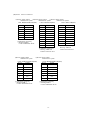
784
448
399.36
715.68
Pixel pitch(horizontal)
Sub- pixel pitch(horizontal)
0.84mm
R G B R G B R G B
R G B R G B R G B
R G B R G B R G B
0.39 mm
Pixelpitch(Vertical)
R G B R G B R G B
R G B R G B R G B
R G B R G B R G B
-1-
0.28mm
1.2 Feature
1. For high definition television by ALIS method
2. For FAN Less design(Low consumption electric power)
3. Thin Depth and Lightness
4.
1.3
Customizing of module equipped with communication function
Specification
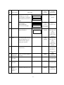
1.3.1 Functional specification
Item
Externals
NO
UA-1x
784 x 448 x 65.5 mm
13 kg
715.68 x 399.36 mm
(32inch: 16:9)
16:9
852 x 1024 pixel
0.84(H) x 0.39(V) mm
0.28(H) x 0.39(V) mm
Module size
Weight
Display size
1
2
3
Aspect ratio
Resolution
Pixel pitch
Sub pixel pitch
4
5
6
7
Color
Grayscale (standard)
8
BrightNess
White (display load
Ratio 1%, standard)
(x,y), white 10%
9
10
(0.300, 0.290) (TYP.)
Contrast in Darkroom (60Hz)
11
500:1 (TYP.)
Video signal
(RGB each color)
Dot clock (max)
12
LVDS (8bit)
13
52 MHz
Horizontal Sync Signal (max)
14
50KHz (LVDS)
Vertical Sync Signal
15
50Hz ± 19/60 ± 1.7Hz
(LVDS)
Input voltage/current
16
100-120/200-240VAC
4.0-1.7A 50/60Hz
Standby electric power (max)
Shade noise at 18dB(A) or less
Temperature (operation)
Temperature (storage)
Humidity (operation)
Humidity (storage)
17
18
19
20
21
22
1W
25dB(A) orless
0 - 55°C
0 - 55°C
20 - 85%RH (no condensation)
20 - 80%RH (no condensation)
Display panel
Chromaticity
Coordinates
Contrast
Data signal
Sync Signal
Powersupply
Noise
Guarantee
environment
RGB each color
256 Grayscale
650 cd/㎡ (TYP.)
Specification
UA-6x
←
←
←
←
←
←
←
←
←
←
←
←
←
←
←
←
←
←
←
←
+3.3/+5/+70-90/+
30-70VDC
0.05/6/ 2.5 /2A
←
←
←
←
←
←
※ It is made to give priority when there is a delivery specification according to the customer.
-2-
UA-7x
←
←
←
900cd/㎡
(typ.)
(0.300,0.300)
(typ.)
900:1
(typ.)
←
←
←
50Hz±1.9/60±
1.7
/70Hz±1.5Hz
(LVDS)
+3.3/+5/+70-90/
+30-65VDC
0.05/6/ 2.5 /2A
←
←
←
←
←
←
1.3.2 Display quality specification
Item
Non-lighting
cell defect
Non-extinguish
ing cell defect
Flickering cell
defect
High intensity
cell defect
Brightness
variation
Color variation
Specification
NO
Total number (subpixel)
Density (subpixel/cm2)
1
2
Size(HxV)
3
(subpixel)
Total number (subpixel)
4
Density (subpixel/ cm2)
5
Flickering lighting cell defect
(sub pixel/ cm2)
Flickering non-extinguishing cell
defect
Twice or more bright point
6
White block of 10% load
[9 point](%)
In area adjacent 20mm
[White](%)
White block of 10% load
[9 point]
7
UA-1x
15 or less
2 or less
(However,1 continuousness or less)
1x2 or less,
Or 2x1 or less
6 or less
(each color 2 or less)
Each color 2 cells max
(However,1 continuousness or less)
5 or less
UA-6x
UA-7x
←
←
←
←
←
←
←
←
←
←
←
←
←
←
8
Number on inside of
Non-extinguishing cell defect
0
←
←
9
20 or less
←
←
10
10 or less
←
←
11
X: Average ±0.015
y: Average ±0.015
←
←
Note: It is made to give priority when there is a delivery specification according to the customer.
-3-
1.3.3
I/0
Interface Specification
(1) I/O signal
No.
Item
Signal Name
Reflection
signal
Timing
Signal
1
RXIN0RXIN0+
RXIN1RXIN1+
RXIN2RXIN2+
RXIN3RXIN3+
Number
of
signals
I/O
Input
LVDS
Differe
ntial
Input video and timing signals
after differential serial
conversion using a dedicated
transceiver.
The serial data signal is
transmitted seven times faster
than the base signal.
Differential clock signal.
Clock
RXCLKINRXCLKIN+
1
1
Input
LVDS
Differe
ntial
Power down
Signal
PDWN
1
Input
LVTTL
SDA
1
I/O
Communication
2
Content of definition
Differential serial data signal.
1
1
1
1
1
1
1
1
Display
Data
MPU
Comm
unicati
on/
Control
Form
LVTTL
(I2C)
SCL
1
I/O
CPUGO
1
Input
LVTTL
PDPGO
1
Input
LVTTL
Input the clock signal after
differential conversion using a
dedicated transceiver.
The clock signal is transmitted
at the same speed as the base
signal.
Low: LVDS receiver
outputs are all L.
High: Input signals are
active.
I2C bus serial data
communication signal.
Communication with the
control MPU of this product is
enabled.
Low power consumption mode
of the control MPU of this
product is released.
“High”:
Control
IRQ
1
Output LVTTL
-4-
This product is started.
(CPUGO=“High” Effective)
It changes into "Low" Î "High"
when this product enters the
undermentioned state.
1.Vcc/Va/Vs output decrease
2.Circuit abnormality detection
(2) LVDS Signal Definition and Function
A video signal (display data signal and control signal) is converted from parallel data to serial data with the LVDS
transmitter and further converted into four sets of differential signals before input to this product.
These signals are transmitted seven times faster than dot clock signals.
The dot clock signal is converted into one set of differential signals by the transmitter before input to this product.
The LVDS signal definition and function are summarized below:
Signal name
Symbol
Number
of signals
RXIN0RXIN0+
1
1
RXIN1RXIN1+
1
1
RXIN2RXIN2+
1
1
Signal definition and function
Display data signal
R0,R1,R2,R3,R4,R5,G0
Display data signal
G1,G2,G3,G4,G5,B0,B1
Video signal
Timing signal
Transmission line
Clock transmission line
RXIN3RXIN3+
1
1
RXCLKINRXCLKIN+
1
1
Display data signal, Sync Signal, Control signal
B2,B3,B4,B5
_____ _____
Hsync, Vsync,
_______
BLANK
Display data signal, Control signal
R6,R7,G6,G7,B6,B7,PARITY
Clock signal
_____
DCLK
-5-
(3)
Video Signal Definition and Function
The table below summarizes the definitions and functions of input video signals before
LVDS conversion.
Item
Original
Display
signal
(before
LVDS
transmitta
nce)
Signal name
Video signal
(digital RGB)
Data Clock
DATA-R
DATA-G
DATA-B
DCLK
Number
of
signals
8
8
8
Input/
output
Input
1
Input
Horizontal sync
signal
_____
Hsync
1
Input
Vertical sync
signal
_____
Vsync
1
Input
PARITY
1
Input
1
Input
Parity signal
Blanking signal
BLANK
-6-
Signal definition and function
Display data signal
R7/G7/B7 is the highest intensity bit.
R0/G0/B0 is the lowest intensity bit.
Display data timing signal: Data are read
when DCLK is low. DCLK is continuously
input.
Regulates one horizontal line of data: Begins
control of the next screen when Hsync is
lowered.
Screen starts up control timing signal: Begins
control of the next screen when Vsync is
lowered.
Input the same frequency in both
odd-numbered and even-numbered fields.
This signal specifies the display field.
H: Odd-numbered field
L: Even-numbered field
Parity signal should be alternated in every
Vsync cycle. This signal is arbitrarily
reversed internally when there is no reversing
signal.
Display period timing signal.
H indicates the display period and L indicates
the non display period.
Note:
Set this timing properly like followings, as is
used internally for signal processing.
・Set the blanking period so that the number
of effective display data items in one
horizontal period is 852.
・Set the number of blanking signals in one
vertical period to 512, which is one half the
number of effective scan lines.
If the BLANK changes when the Vsync
frequency is switched, the screen display may
be disturbed or brightness may change.
The screen display is restored to the normal
state later when the BLANK length is
constant again.
(4) Connector Specifications
The connector specification is shown below.
Please do not connect anything with the terminal NC.
(I) Signal connector CN1: DF13-20DP-1.25 V (tin-plated) (Maker: HIROSE DENKI)
Pin No.
Signal name
Pin No.
Signal name
1
RXIN0-
2
GND
3
RXIN0+
4
SCL
5
RXIN1-
6
GND
7
RXIN1+
8
SDA
9
RXIN2-
10
GND
11
RXIN2+
12
CPUGO
13
RXCLKIN-
14
PDPGO
15
RXCLKIN+
16
IRQ
17
RXIN3-
18
PDWN
19
RXIN3+
20
GND
[Conforming connector]
Housing: DF13-20DS-1.25C
Contact: DF-2630SCF
(II) Power Source Connectors for power supply(jig)
(a) Power input connector
(b) Power supply output connector for system
CN61: B06P-VH
CN62:B03P-VH
(Maker: JST)
(Maker: JST)
Pin No.
Symbol
Pin No.
Symbol
1
2
3
VAUX
N.C
GND
1
2
3
4
AC(L)
N.C
AC(N)
N.C
5
N.C
6
F.G
[Conforming connector]
Housing: VHR-06N (or M)
Contact: SVH-21T-P1.1
[Conforming connector]
Housing: VHR-03N (or M)
Contact: SVH-21T-P1.1
(c) Power supply output connector for system
CN63: B5B-XH-A
(Maker: JST)
Pin No.
Symbol
1
Vpr1
2
N.C.
3
Vpr2
4
N.C.
5
GND
[Conforming connector]
Housing: XHP-5
Contact: SXH-001T-P0.6
-7-
(III) Power Source Connectors
(a)Power supply output
(b)Power supply output
connector for system
(c)Power supply output
connector for system
CN6: B6B-PH-SM3-TB(JST)
connector for system
CN23: B10PS-VH(JST)
CN33: B9PS-VH(JST)
Pin No.
Symbol
Pin No.
Symbol
Pin No.
Symbol
1
Vpr2
1
Va
1
Vcc
2
N.C.
2
N.C.
2
GND
3
4
5
6
GND
GND
N.C.
Vcc
3
4
5
6
7
8
9
10
Vcc
GND
GND
GND
N.C.
Vs
Vs
Vs
3
4
5
6
7
8
9
GND
GND
GND
N.C.
Vs
Vs
Vs
[Conforming connector]
Housing: PHR-6
Contact: SPH-002T-P0.5L
[Conforming connector]
Housing: VHR-10N
Contact: SVH-21T-P1.1
(d)Power supply output
(e)Power supply output
connector for system
CN42: B7B-PH-SM3-TB(JST)
connector for system
CN52: B7B-PH-SM3-TB(JST)
Pin No.
Symbol
Pin No.
Symbol
1
Va
1
Va
2
N.C.
2
N.C.
3
N.C.
3
N.C.
4
GND
4
GND
5
GND
5
GND
6
N.C.
6
N.C.
7
Vcc
7
Vcc
[Conforming connector]
Housing: PHR-7
Contact: SPH-002T-P0.5L
[Conforming connector]
Housing: VHR-9N
Contact: SVH-21T-P1.1
[Conforming connector]
Housing: PHR-7
Contact: SPH-002T-P0.5L
-8-
(f)Power supply output
connector for system
CN7: 00 6200 520 330 000 [ZIF Right Angle Connector](kyousera elco)
Pin No.
Symbol
Pin No.
Symbol
1
2
3
4
5
6
7
8
9
10
N.C.
N.C.
N.C.
N.C.
GND
VSAGO
GND
VCEGO
GND
PFCGO
11
12
13
14
15
16
17
18
19
20
GND
Vra
GND
Vrs
GND
Iak
GND
Vak
GND
Vsk
-9-
2.
Notes on safe handling of the plasma display
2. 1
Notes to follow during servicing
The work procedures shown with the Note indication are important for ensuring the safety of the
product and the servicing work. Be sure to follow these instructions.
Before starting the work, secure a sufficient working space.
At all times other than when adjusting and checking the product, be sure to turn OFF the main
POWER switch and disconnect the power cable from the power source of the display (jig or the
display itself) during servicing.
To prevent electric shock and breakage of PC board, start the servicing work at least 30 seconds after the
main power has been turned off. Especially when installing and removing the power supply PC board
and the SUS PC board in which high voltages are applied, start servicing at least 2 minutes after the
main power has been turned off.
While the main power is on, do not touch any parts or circuits other than the ones specified.
The high voltage power supply block within the PDP module has a floating ground. If any
connection other than the one specified is made between the measuring equipment and the high
voltage power supply block, it can result in electric shock or activation of the leakage-detection
circuit breaker.
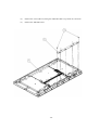
When installing the PDP module in, and removing it from the packing carton, be sure to have at least two
persons perform the work while being careful to ensure that the flexible printed-circuit cable of the PDP
module does not get caught by the packing carton.
When the surface of the panel comes into contact with the cushioning materials, be sure to confirm
that there is no foreign matter on top of the cushioning materials before the surface of the panel comes
into contact with the cushioning materials. Failure to observe this precaution may result in the surface
of the panel being scratched by foreign matter.
When handling the circuit PC board, be sure to remove static electricity from your body before
handling the circuit PC board.
Be sure to handle the circuit PC board by holding the such large parts as the heat sink or transformer.
Failure to observe this precaution may result in the occurrence of an abnormality in the soldered areas.
Do not stack the circuit PC boards.
Failure to observe this precaution may result in problems resulting from scratches on the parts, the
deformation of parts, and short-circuits due to residual electric charge.
Routing of the wires and fixing them in position must be done in accordance with the original routing
and fixing configuration when servicing is completed.
All the wires are routed far away from the areas that become hot (such as the heat sink). These
wires are fixed in position with the wire clamps so that the wires do not move, thereby ensuring
that they are not damaged and their materials do not deteriorate over long periods of time.
Therefore, route the cables and fix the cables to the original position and states using the wire
clamps.
Perform a safety check when servicing is completed.
Verify that the peripherals of the serviced points have not undergone any deterioration during
servicing. Also verify that the screws, parts and cables removed for servicing purposes have all
been returned to their proper locations in accordance with the original setup.
-10-
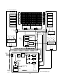
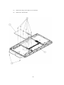
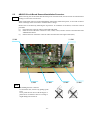
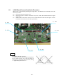
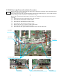
3. Name and Function
3.1 Configuration
③Y-SUS board
Panel chassis
⑥PSU board *1
Product label
Serial Id label
②X-SUS board
Scan module
⑧Signal
cable
⑦Ps cable
ADM1
ADM2
ADM3
ADM4
ADM5
ADM6
ADM7
⑩PSU
Signal cable
XBB
Address module(ADM)
④ABUSL board
⑤ABUSR board
①LOGIC board
The figure shows the article number in the parts information table of clause 7.
*1:Power supply(jig)
-11-
3.2 Block Diagrams
3.2.1 Signal Diagrams
Y-SUS B.
Y-SUS
EVEN SW
X
B
B
S
D
M
X-SUS B.
X-SUS
EVEN SW
X-SCAN
EVEN SW
Y-SCAN
EVEN SW
S
D
M
Y-SUS
ODD SW
Y-SCAN
ODD SW
X
B
B
X-SUS
ODD SW
X-SCAN
ODD SW
ADM1 ADM2 ADM3 ADM4 ADM5 ADM6 ADM7
ABUSR B.
ABUSL B.
POS /NEG
RESET SW
CN51
POS
RESET SW
CN41
CN31
CN21
TIMMING ROM
LOGIC B.
CN3
CN2
SCAN CONTROLLER
OSC
24MHz
SIGNAL
INPUT
DATA CONVERTER
DATA PROCESSOR
CN1
LVDS
γ comp.
RGB
GAIN
DITHER
/ERR DIF.
SUB FIELD
PRC.
MEMORY
CN5
CONTROLLER
CN4
MPU
V-SYNC cont.
I2 C
Analog SW
OSC
OSC
50MHz
SCI.
Failure DET.
OSC
80MHz
EEPROM
APC cont.
FLASH
D/A
I/O
8MHz
CN7
-12-
PFCgo
Vsago
Vcego
Vrs
Vra
Vrw
Vrx
FRAME
MEMORY
3.2.2 Power Diagrams
X-SUS B.
Y-SUS B.
Y-SUS
EVEN SW
S
D
M
X
B
B
Y-SCAN
EVEN SW
Y-SUS
ODD SW
Y-SCAN
ODD SW
X-SUS
EVEN SW
X-SCAN
EVEN SW
S
D
M
X
B
B
ADM1
POS/NEG
ADM2
ADM3
ADM4
ADM5
ADM6
Vcc 5V
Va 55V
Vcc 5V
X-SCAN
ODD SW
ADM7
POS
ABUSR B.
ABUSL B.
RESET SW
X-SUS
ODD SW
RESET SW
Va 55V
Va
Vw 160V
Vb -5V
CN32
CN52
5V
YFVCC2
YFVE2
VE
17V
17V
17V
DC/DC
CONVERTER
D/A
CPUgo
PDPgo
Vs 80V
Vra
Vrs
Vrw
Vrx
17V
YFVE1
XFVCC1
Vcc 5V
Vs 80V
RST
Vrst
LOGIC B.
5V
VEW
17V
XFVE1
XFVE2
VE
17V
17V
17V
DC/DC
CONVERTER
Vcc 5V
CN6
CN33
XFVCC2
5V
MPU
Vpr2 3.3V
45V
DC/DC
CONVERTER
FVE5H
5V
Vcc 5V
Vx
-5V
CN22
CN42
Vxwgo
YFVCC1
Vb
Vs 80V
CN23
AC100 240V
10A
PFC
380V
55V
Va
CN61
Vsago
CN65
5V
Vcc
Servce
SW
CN68
Vcego
Vs
80V
CN67
PFCgo
Vpr2
Vpr1
5/3.3V
Control
PFCgo
Vsago
Vcego
CN66
3.3V
5V
Vsago
CN64
Vra Vrs
PSU B. *1
-13-
*1:Power supply (jig)
3.3 Function
3.3.1 Logic board Function
(1) Data Processor
z
γadjustment (1/2.2/2.4/2.6/2.8)
z
NTSC/EBU format(Color matrix)Switch
z
RGB gain Control(White balance adjustment、Amplitude limitation)
z
Error Diffusion Technology (Grayscale adjustment)
z
Dithering (Grayscale adjustment)
z
Burn-in Pattern generation
(2) Scan Controller
z
Address driver control signal generator (ADM)
z
Scan driver control signal generator (SDM)
z
X/Y sustain control signal generator
(3) Waveform ROM
z
Waveform Pattern for drive / Timing memory
(4) MPU
z
Synchronous detection
z
System control
z
Driving voltage (Va,Vs,Vr,Vw) adjustment and tuning
z
Abnormal watching (breakdown detection) / abnormal processing
z
Is (sustain) current control (sustain pulse control)
z
Ia (address) current control (sub-field control)
z
External communication control
z
Waveform ROM pattern writing
(5) EEPROM
z
Control parameter memory
z
The accumulation energizing time (Every hour).
z
Abnormal status memory (16 careers)
-14-
Sub Data
Address bit
00
7-0
7
01
02
Symbol
Item
Function
Setting [hex]
RANGE
INITIAL value
00 ~ FF
01【UA1x/6x】
02【UA7x 】
MAPVER
address MAP
Version
Indicates the version number of the address
map.
ERRF
update of Error
Flag
Indicates that an error has occurred.
It can be cleared with the ErrRST setting.
If this flag is set,
• Error code is written.
• Cannot enter the PDP-ON mode.
0: Not updated
1: Updated
0
6
OHRF
update of
Operation Hours
Flag
Indicates that the drive hours are counted.
0: Not updated
1: Updated
0
5
PSDF
Power Shut
Down Flag
Indicates that shutdown of the AC power is
detected and the PDP has executed the
OFF-sequence. It can be cleared with the
PSDRST setting.
0: Not detected
1: Detected
0
4-0
CNDC
Condition Code
Indicates status of the module.
-
-
Error Code
Indicates error code.
The error codes of as many as 16 errors in
the past can be retrieved with the ERRS
setting. . Same error code is not stored
00~FF
00
7-0
ERRC
continuously.
03
7-0
OHRH
Operation Hours
Higher bits
Indicates the higher 8 bits of the module
driving hours. *1)
00~FF
00
04
7-0
OHRL
Operation Hours
Lower bits
Indicates the lower 8 bits of the module
driving hours. *1)
00~FF
00
0: The single
color display
is switched
every 2
seconds. A
total of 8
colors are
displayed.
1: All white
(Different
from actual
white.)
0
0: Displaying
the input
signal
1: Displaying
the built-in
pattern
0
0: Blank
1: Displaying
the input
signal
1
It selects the built-in test pattern signals of
this display. This setting is valid when the
PATON setting is 1.
7
PATSEL
Selecting
patterns
Display of the built-in pattern signal in this
product is turned ON/OFF.
6
PATON
Built-in pattern
display is set to
ON.
5
ADEN
Address
data
enable
The black screen is displayed.
0 is set when the input video signal has
disturbance.
4
-
-
Be sure to use the display with the setting
fixed to 0.
3
-
-
DSPPRT
DiSPlay
PaRiTy
20
3
Be sure to use the display with the setting
fixed to 1.
Input reflection polarity setting
-15-
0~1
0
0~1
1【UA1x/6x】
0:Emits light by
LOW
1:Emits light by
High
1【UA7x
】
Setting [hex]
Sub Data
Address bit
Symbol
Item
20
2
IFON
Interface power
supply ON
1
PDPON
High voltage
power supply
ON
Function
Switches the interface power ON/OFF.
Use this item when you want turn ON the
main power of the interface side only when
the PDPON is set to 0. This setting is
invalid when PDPON is set to 1.
Switches ON/OFF the high voltage power
supply of PDP.
RANGE
INITIAL value
0: Power OFF
1: Power ON
0
0: Power OFF
1: Power ON
0
Be sure to use the display with the setting
fixed to 1.
0
0~1
1
*1) It is not the one to guarantee brightness.
Sub Data
Address bit
Symbol
Item
Function
Setting[hex]
RANGE
INITIAL value
7-5
-
-
Be sure to use the display with the setting
fixed to 0.
0~7
0【UA1x/6x】
7-6
-
-
Be sure to use the display with the setting
fixed to 0.
0~7
0【UA7x】
4
CCFMD
Color correction
mode
3
DCBON
Selecting the color correction modes.
Valid when the CCFON setting is 1
0: Luminance
has priority.
1: Gradation
has priority
0
Dynamic Color
Balance
Tracking correction of white balance
between the high luminance and the low
luminance.
0: OFF
1: ON
0
2
HAON
Heat APC
function
When a picture with high luminance/small
area is displayed for about 3 minutes or
longer, the number of pulses is reduced to
about 20% at a maximum. This item can be
used to reduce panel temperature/extend
useful life when the display is used to
show a still image.
1
-
-
Be sure to use the display with the setting
fixed to 0.
21
0: OFF
0
1: ON
0~1
0
Whether the register value is reflected to
the operating status of this product,
selected by this item.
The following switch is executed.
0
22
0: The received register value is reflected
from the next field.
Color collection process is turned
ON/OFF.
1: The received register value is stored so
that the DSET setting is reflected from
the next field.
(DSET setting: Setting bit 0 of address
FF)
7
CCFON
Color correction
6
CCFORM
Color correction
format
-
-
Be sure to use the display with the setting
fixed to 0.
Item
Function
5-3
Sub
DSETEN
Data
set
enable
Data
Symbol
Color collection process is switched.
This item is valid when CCFON setting is
1.
0: Invalid
1: Valid
0: OFF
1: ON
0
0: NTSC
1: EBU
0~7
Setting [hex]
-16-
1
0
0
Addre
ss
bit
Reverse γ correction level is set.
The setup 7 is the test mode. Do not select
the setup 7.
22
2-0
GAMSEL
Selecting the
reverse γ
correction
23
7-0
CONTRAS
T
Peak luminance
24
7-0
R-RATIO
R ratio
25
7-0
G-RATIO
G ratio
26
7-0
B-RATIO
B ratio
6
ERRRST
5
-
-
Be sure to use the display with the setting
fixed to 0.
Sub
ERRS
00~FF
FF
00~FF
FF
00~FF
FF
0: Normal
1: IRQ signal
clear
0
0: Normal
1: ERRF
flag clear
0
0~1
0【UA1x/6x】
Clearing the
OHRF flag
The control by which the OHRF flag is
returned to 0 is done. This setting
automatically returns to the state of 0 after
returning 0 the ERRF flag when this
setting is set to one.
0: Normal
1: OHRF
flag clear
Clearing the
PSDF flag
This item exercise control to return the
PSDF flag to 0 when this machine
performs the OFF sequence at AC power
shutdown. When this item is set to 1, this
setting automatically returns to 0 after
returning the PSDF flag to 0.
0: Normal
1: PSDF
flag
clear
0
When this setting is changed and the
ERRC setting is read out, the error
contents (as many as 16 errors) of the
module that have occurred in the past can
be checked.
If more than 16 errors have occurred, the
error code is updated starting from the
oldest error.
0: Latest error
1: Previous
error
2:
|
E:
F:Oldest error
0
27
3-0
FF
Use the display with at least one item being
set to FF (hex).
This item implements control to return the
ERRF flag to 0 when an error occurs.
When this item is set to 1, this setting
automatically returns to 0 after returning
the ERRF flag to 0.
PSDRST
00~FF
White balance is adjusted.
Clearing the
ERRF flag
4
2
When the display picture load is heavy, the
peak luminance is automatically limited.
Clearing the IRQ
output signal
OHRRST
0: OFF
1: 1.0 th power
2: 2.2 nd
power
3: 2.4 th power
4: 2.6 th power
5: 2.8 th power
6: USER
7: TEST
Peak luminance is adjusted.
IRQRST
5
28
When the setup 6 is selected, setting of the
addressed in the range of 31~51 become
valid.
This item implements control to return the
IRQ signal from "HIGH" to "Low" level
when an error occurs. When this item is set
to 1, the IRQ signal is returned to "Low"
level.
7
INITIAL
value
RANGE
Error code
selection
-
-
Be sure to use the display with the setting
fixed to 0.
0~3
7
PWMP
Power Maximam
peek control
The PWMAX setting is switched to
constant brightness (peak electric power)
control. The password setting is necessary
to turn on this setting.
When password
is set
0:OFF 1:ON
Data
Symbol
Item
Function
7-6
0【UA7x】
0【UA1x/6x】
0【UA7x】
Setting [hex]
-17-
Addre
ss
bit
6
28
5-4
-
PWMAX
-
Be sure to use the display with the setting
fixed to 0.
Maximum power
consumption
Sets the maximum power consumption.
Set this item in accordance with the status
of the machine.
Make sure that the respective parts'
temperature/panel temperature stays within
the specifications. If the setting is set to 3,
power consumption increases to a level
exceeding the standard consumption. Be
sure to execute the heat dissipation design
so that respective parts' temperature/panel
temperature stays within the specifications.
Setting of the maximum electric
power.
0: 0W
1: +10W
2: +20W
3: +30W
PWMP
=1
Setting of peak electric power.
Electric power by which electric
power is permitted in addition to
improve practical brightness to
the maximum electric power set
3:+10W
0: −20W
1: −10W
2: ±0W
3: +10W
2【UA1x/6x】
Maximum power
consumption
3-0
-
-
Be sure to use the display with the setting
fixed to 0.
0-F
Password of peak
electric power
setting
Password of peak electric power
setting.The password is described to the
delivery specifications. When the password
setting is normally done, the reading value
of the real thing ground becomes 51.
51: Permission
of PWMP
ON
Another:
Prohibition
Ps-Tank PoWer
The maximum
electric power
setting:
The maximum
over electric power
from +10W
7-0
PWM
PASS
PsTPW
When the amount of
an over electric
power becomes
PsTPW×PsTTM or
less at PWMP=1, the
control by which
brightness is lowered
is done.
2D
7-0
PsTTM
Ps-Tank TiMe
31
7-0
GAM00
Reverse γ
correction DC
Sets the input level that implements the
forced 0 [LSB] output.
7-2
-
<no use>
-
1-0
GAM01
[9: 8]
7-0
GAM01
[7: 0]
Reverse γ
coefficient 01
Reverse γ coefficient value is set.
Input Output value of 8 [LSB]
7-3
-
<no use>
-
Reverse γ
correction 02
Reverse γ coefficient value is set.
Input Output value of 16 [LSB]
Item
Function
34
0: −20W
1: −10W
2: ±0W
3: +10W
PWMP
=0
Time which can
operate by the
maximum over
electric power
(*10sec)
33
0【UA7x】
PWMAX
7-0
32
0-3
5-4
29
2C
INITIAL
value
RANGE
2-0
GAM02
[10: 8]
35
7-0
GAM02
[7: 0]
Sub
Data
Symbol
2【UA7x】
0
FF【UA7x】
00-FF
1E【UA7x】
00-FF
3C【UA7x】
00~FF
1F
00~FF
00
00~FF
04
00~FF
00
00~FF
24
Setting [hex]
-18-
Addre
ss
36
37
bit
7-4
-
<no use>
-
3-0
GAM03
[11:8]
Reverse γ
correction 03
Reverse γ coefficient value is set.
7-0
7-4
38
3-0
39
7-0
7-5
3A
3B
3C
3D
3E
3F
40
41
42
43
Sub
4-0
7-1
GAM03
[7: 0]
-
<no use>
-
GAM04
Reverse γ
correction 04
Reverse γ coefficient value is set.
Input Output value of 32 [LSB]
[11: 8]
GAM04
[7: 0]
-
<no use>
GAM05
Reverse γ
correction 05
0
-
<no use>
-
-
<no use>
-
7-1
GAM06
GAM06
Reverse γ
correction 06
[7: 1]
0
-
<no use>
-
-
<no use>
-
7-2
GAM07
[12: 8]
GAM07
Reverse γ
correction 07
[7: 2]
-
<no use>
-
7-5
-
<no use>
-
7-2
GAM08
[12: 8]
GAM08
Reverse γ
correction 08
[7: 2]
-
<no use>
-
7-6
-
<no use>
-
7-4
GAM09
[13: 8]
GAM09
Reverse γ
correction 09
00
00~FF
A7
00~FF
01
00~FF
12
00~FF
01
00~FF
9A
00~FF
02
00~FF
40
00~FF
03
00~FF
04
00~FF
04
00~FF
F0
Reverse γ coefficient value is set.
Input
Output value of 64 [LSB]
1-0
5-0
00~FF
Reverse γ coefficient value is set.
Input
Output value of 56 [LSB]
1-0
4-0
58
Reverse γ coefficient value is set.
Input
Output value of 48 [LSB]
7-5
4-0
00~FF
Reverse γ coefficient value is set.
Input
Output value of 40 [LSB]
[7: 1]
[12: 8]
00
-
GAM05
[12: 8]
00-FF
Input Output value of 24 [LSB]
7-5
4-0
INITIAL
value
RANGE
Reverse γ coefficient value is set.
Input
Output value of 80 [LSB]
[7: 4]
3-0
-
<no use>
-
Data
Symbol
Item
Function
Setting [hex]
-19-
Addre
ss
bit
7-6
44
45
46
47
48
-
<no use>
-
GAM10
Reverse γ
correction 10
Reverse γ coefficient value is set.
Input
Output value of 96 [LSB]
[7: 4]
Reverse γ
correction 10
Reverse γ coefficient value is set.
Input
Output value of 96 [LSB]
3-0
-
<no use>
-
7-6
-
<no use>
-
5-0
7-4
5-0
7-4
4C
4D
4E
4F
50
51
Sub
GAM11
[13: 8]
GAM11
Reverse γ
correction 11
Reverse γ coefficient value is set.
Input
Output value of 112 [LSB]
[7: 4]
<no use>
-
7-6
-
<no use>
-
7-4
4B
GAM10
-
49
4A
[13: 8]
3-0
5-0
GAM12
[13: 8]
GAM12
Reverse γ
correction 12
[7: 4]
-
<no use>
-
7-6
-
<no use>
-
7-4
GAM13[1
3: 8]
GAM13[7:
Reverse γ
correction 13
Reverse γ coefficient value is set.
Input
Output value of 160 [LSB]
4]
3-0
-
<no use>
-
7-6
-
<no use>
-
5-0
7-4
GAM14[1
3: 8]
GAM14[7:
Reverse γ
correction 14
4]
3-0
-
<no use>
-
-
<no use>
-
7-4
GAM15[1
3: 8]
GAM15[7:
Reverse γ
correction 15
Reverse γ coefficient value is set.
Input
Output value of 224 [LSB]
4]
3-0
-
<no use>
-
7
-
<no use>
-
6-0
7-5
GAM16[1
4: 8]
GAM16[7:
Reverse γ
correction 16
-
<no use>
Data
Symbol
Item
00~FF
60
00~FF
0A
00~FF
50
00~FF
0D
00~FF
D0
00~FF
16
00~FF
A0
00~FF
21
00~FF
E0
00~FF
2F
00~FF
90
00~FF
40
00~FF
00
Reverse γ coefficient
Input
Output value of 256 [LSB]
5]
4-0
07
Reverse γ coefficient value is set.
Input
Output value of 192 [LSB]
7-6
5-0
00~FF
Reverse γ coefficient value is set.
Input
Output value of 128 [LSB]
3-0
5-0
INITIAL
value
RANGE
Function
Setting [hex]
-20-
Addre
ss
bit
E5
7-0
UVrs
USER Vrs
7-0
UVra
USER Vra
7-3
-
<no use>
E6
2
RCLVr
UVrs/UVra
RECALL
1
EWRVr
UVrs/UVra
Write
0
-
-
7-1
-
-
DSET
Data setup
FE
FF
0
00~AA
INITIAL
value
Adjusted in
factory
Adjusted in
factory
0
0
RANGE
Setting Vrs voltage
Standard equation: Vrs=2.99*UVrs/255
Setting Vra voltage
Standard equation: Vra=2.99*UVra/255
Be sure to use the display with the setting
fixed to 0.
Resetting the UVrs, UVra in both of
register and EEPROM to the initial value
by setting RCLVr to 1.
This setting automatically returns to 0 after
resetting the UVrs,Uvra.
Storing the UVrs,UVra
in register to
EEPROM by setting EWRVr to 1.
This setting automatically returns to 0 after
resetting the UVrs,Uvra.
Be sure to use the display with the setting
fixed to 0.
Be sure to use the display with the setting
fixed to 0.
When the DSETEN setting is 1, setting
this bit causes all the register setups that
have been set up to now, to be reflected to
the operation status of this product. They
are reflected from the next field after this
bit is accepted.
-21-
00~AA
0:Normal
1:UVrs,UVra
initialized
0
0:Normal
1:UVrs,UVra
stored
in EEPROM
0
0
0
0
0
0: Normal
1: Execute
0
3.3.2
Function of X-SUS Board
(1) DC/DC power supply block
Vs (+80V) Î Vw (+180V)/Vx (+45V) 【UA-1x/6x】
Vs (+80V) Î Vw (+170V)/Vx (+60V) 【UA-7x】
Vcc (+5V) Î XFvcc (+5V, floating)/XFve (+17V, floating)/Ve (+17V)/Vb(-5V)
(2) X switching block
Switching during address period
Switching during sustain period
Switching during reset period
(3) Current detector block
Isx (sustain) current detection
3.3.3
Function of Y-SUS Board
(1) DC/DC power supply block
Vcc (+5V) Î Y Fvcc (+5V, floating)/Y Fve (+17V, floating)/Ve (+17V)
(2) Switching block
Switching during address period
Switching during sustain period
Switching during reset period
(3) Current detector block
Isy (sustain) current detection
Isp (SDM) current detection
3.3.4
Function of PSU Board (jig)
(1) Standby power supply block
AC100–200 Î Vpr1 (+5V)/Vpr2 (+3.3v)
(2) PFC block (AD/DC power supply block)
AC100–200 Î 380V
(3) AD/DC power supply block
+380V Î Vcc (+5V) / Vs (+80V)/Va (+55V)
(4) Current detection block
Ia (address) current detection
(5) Abnormal voltage monitoring
Vs excess voltage monitoring
Va excess voltage monitoring
-22-
3.4 Protection function
State of protection operation (×:State change , There is no change at the blank)
Abnormality part
State
Vw
Vx
Vs
Va
Vex
Vey
Vcc
Vpr1
Vpr2
PSU
Heat
sink
Vx
Vs
Va
Vex
Vey
Vcc
Vpr
Vau
x
Overvoltage
Stop(no latch)
×
×
×
×
×
×
×
Overcurrent
Delay Latch
×
×
×
×
×
×
×
Overvoltage
Stop(no latch)
×
×
×
×
×
×
×
Overcurrent
Delay Latch
×
×
×
×
×
×
×
Overvoltage
Latch
×
×
×
×
×
×
×
Low voltage
Latch
×
×
×
×
×
×
×
Overcurrent
Delay Latch
×
×
×
×
×
×
×
Overvoltage
Latch
×
×
×
×
×
×
×
Low voltage
Latch
×
×
×
×
×
×
×
Overcurrent
Delay Latch
×
×
×
×
×
×
×
Overvoltage
Stop(no latch)
×
×
×
×
×
×
×
Overcurrent
Voltage
pendency
(no latch)
×
×
×
×
×
×
×
Overvoltage
Latch
×
×
×
×
×
×
×
Overcurrent
Delay Latch
×
×
×
×
×
×
×
Overvoltage
Latch
×
×
×
×
×
×
×
×
×
○
Delay Latch
×
×
×
×
×
×
×
×
×
○
Delay Latch
×
×
×
×
×
×
×
×
×
○
Latch
×
×
×
×
×
×
×
×
×
○
Voltage pendency
×
×
×
×
×
×
×
×
×
×
×
×
×
×
×
×
○
Overcurrent
Overcurrent
Overvoltage
Vaux
Vw,
Reactivation
condition when
abnormal content is
excluded
AC
PFCgo
Re-turni
Reset
ng on
○
○
○
○
Overcurrent
(Note 2)
Temperature
○
○
○
○
○
○
○
○
○
○
○
○
○
○
○
○
○
○
○
○
○
○
○
○
(no latch)
Latch
-23-
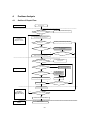
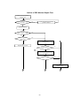
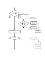
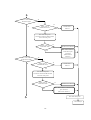
4.
Problem Analysis
4. 1
Outline of Repair Flow
Client
Client claim
Repair product
and Claim contents match
Recheck the problem description
Y
Product block/PDP module block
Locating cause of problem
Product
manufacturer
(Repair center)
Y
Is PDP module block
Defective ?
N
Product problem analysis/Repair
N
PC board replacement/Parts
replacement
Y
Is the Panel defective ?
Y
N
Y
Operation normal ?
PDP module sent to factory
Repair product and
claim contents match
N
Y
Is the panel faulty?
Repair center
Recheck problem
description
Panel replacement/IC
module replacement
N
PC board
unacceptable (NG) ?
Y
PC board
replacement/Parts
replacement
N
Processing to prevent recurrence
Packing/Shipment
Y
Installation in product
Product
manufacturer
(Repair center)
N
Product runs normally ?
Y
Return of repaired product
Client
End of repair
-24-
Heat run
Operation normal ?
N
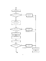
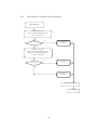
Outline of PDP Module Repair Flow
Receipt of returned product
(Chapter 4.3)
Does ID of
returned product agree with ID
of actual
No
Repair description and returned
product rechecked.
Yes
Appearance check
Yes
Appearance unacceptable
(NG) ?
No
Yes
Repair of appearance
requested ?
No
Yes
4
Perform operation test
(Chapter 4.4).
Repair defective spots
Problem recurred ?
2
No
Yes
Check description of
repair request.
Contents match ?
No
Yes
Problem symptom nonrecurrence
analysis mode
3
1
-25-
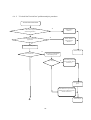
5
1
Fault mode classification (Chapter 4.5)
Fault analysis (Chapter 4.6)
Repair of faulty spots (Chapter 5)
Replace LOGIC PC board or
panel chassis ?
Yes
Adjustment (Chapter 6)
No
3
Perform operation test (Chapter 4.4)
No
Problem repaired?
Yes
Warranty test (Running)
End of repair
Shipment
-26-
Problem symptom nonrecurrence
analysis mode/Shipment process mode
5
Implement module tapping
No
Problem recurs ?
Perform running test (Burn-in pattern)
Yes
Problem recurs ?
Turn off the main power
2
No
Yes
3
-27-
4.3 Checking the Product Requested for Repair
Check the serial ID number of the product requested for repair before starting the problem analysis and
repair.
Structure of serial ID number is shown below.
(1) Checking serial ID number of PDP module (14 digits)
The serial ID number of the product that is brought in for service and that of the completed panel
chassis has the structure as shown below.
The serial ID number is shown on the bar code label that is attached to the rear of the chassis
(aluminum).
N5A
1 01 001A1
01A
Version No.: 01 ~ 99
A ~ Z (excluding I and O)
Lot No.: 001 ~ 999
A ~ Z (excluding I and O)
1~3
Production week code: 01 ~ 53
Production year (low digit): 0 ~ 9
Product code: N5A ,P5A and S5A model 32 H1 type
Module product label
Serial ID label of panel chassis
∗ The module serial ID number and the serial ID number of the completed chassis (product requested for
repair) are usually the same when the product is brought in for repair for the first time.
(2) Checking serial ID number of constituent PC boards (12 digits)
The serial ID number of the module constituent PC boards has the following structure.
The serial ID number is shown on the bar code label that is attached to each PC board.
GG 1 01
0001
01A
Version No.: 01 ~ 99
A ~ Z (excluding I and O)
Lot No.: 0001 ~ Z9999
Production week code: 01 ~ 54
Production year (low digit): 0 ~ 9,A~ K(10-20)
Product code: GG X-SUS board
: GJ Y-SUS board
: GE ABUSR board
: GD ABUSL board
: GF LOGIC board
: -- PSU board
-28-
4.4 Operation Test Procedure
(1) Prepare the test equipment and the module requested for repair.
(2) Affix to the stand (jig) the module requested for repair.
(3) Connect LOGIC board connector CN1 of the module to the Interface board
(jig) CN5 with the dedicated signal cable.
(4) Connect the AC power cable to the module requested for repair.
(5) Turn on the AC power to the interface board (jig).
(6) Select the signal used when a problem occurs, or an all white pattern.
(7) Set the PDP go switch on the Interface board (jig) to ON.
(The main power of the module is turned on.)
Check Fault Symptom
CN1
CN5
PDPgo
ON
OFF
-29-
4.5 Fault Symptom
NO
Fault contents
1
Entire screen
does not light.
2
Suspected
fault
location
Analysis
procedure
and measure
After momentarily going
on, the screen becomes
black immediately or after a
few seconds. (Main power
is turned off.)
X-SUS
Y-SUS
Panel chassis
LOGIC
ABUSL
ABUSR
Refer to
Chapter 4.6.1
Screen lights dimly even on
LOGIC
Replace
Fault status
the back screen.
3
Vertical line
LOGIC board
Panel chassis
LOGIC
Single vertical line (of
different color)
5
Vertical bar
Horizontal
line
8
Panel chassis
Replace panel
chassis
Panel chassis
ABUSL
ABUSR
LOGIC
Bar width of 1/7 of
horizontal size or in
multiples of 1/7, is
displayed. Abnormal
display.
Refer to
Chapter 4.6.2
Above boards
are connected.
ABUSL
ABUSR
LOGIC
Bar width of 3/7 or 4/7 of
the screen width, is
displayed. Abnormal
display. (Vertical line of
different color)
6
7
Chapter 4.6.2
Vertical line from the
middle of effective scan
area (Vertical line of
different color)
4
Refer to
Refer to
Chapter 4.6.2
Above boards
are connected.
Single horizontal line (No
light) Or single horizontal
line does not light among
the effective scanning area.
Single horizontal line does
not light.
Occurrence by one line(No
light) ,full screen
Panel chassis
Replace panel
chassis
X-SUS
Y-SUS
-30-
Replace
X-SUS
Y-SUS
NO
Fault contents
9
Horizontal bar
Fault status
Bar width of 1/8 or
multiples of 1/8 of the
screen height, is displayed.
Suspected
fault
location
Analysis
procedure
and measure
Panel chassis
Replace panel
chassis
Abnormal (Screen does not
light)
Bar width of 1/2 of the
screen height.
Abnormal display
(Screen does not light)
10
11
Image burn-in
Panel chassis
Y-SUS
X-SUS
Fixed display contents are
always displayed.
ABCDEFG
Panel
chassis
Stains
Oval-shaped points having
abnormal luminance are
scattered in the upper or
lower part of screen.
Panel
chassis
13
Flicker
The entire screen flickers
continuously.
Connector
Chrominance
is abnormal
15 Sync is
disturbed
18
Picture
distorted
19
Steps of
gradation are
skipped
Chapter 4.6.3
Above boards
are connected.
12
14
Refer to
Colors cannot be displayed
correctly.
LOGIC
LOGIC
Luminance linearity is poor.
-31-
Perform all
white heat run.
After
judgment,
replace panel
chassis
Perform all
white heat run.
After
judgment,
replace panel
chassis
Reconnecting
of connector
and cable, or
exchanges the
cable.
Replace
LOGIC board
Replace
LOGIC board
LOGIC
Replace
LOGIC board
LOGIC
Replace
LOGIC board
NO
Fault contents
20
Abnormal
Fault status
sound
Suspected
fault
location
Analysis
procedure
and measure
PSU
X-SUS
Y-SUS
Locate cause
of abnormality
(Core is broken,
and viewing.
or transformer
Replace the
is abnormal.)
cause of
from listening
problem.
21
Control on
Contrast, color temperature
external
adjustment and ϒ cannot be
LOGIC
Replace
LOGIC board
communicatio changed.
n is abnormal
-32-
4.6 Problem Analysis Procedure
4.6.1 "The entire screen does not light (Main power is turned off)” problem analysis
procedure
The entire screen does not light.
(Main power is turned off.)
Y
PC for analysis
Connected?
Analysis using PC
Chapter 4.7
N
Remove CN6 (LOGIC)
Turn on AC power.
N
PSU board Vpr2
(3.3V) exists?
PSU board is
defective.
Y
STANDBY power
supply has
abnormality.
Turn off AC power.
Connect CN 6 (LOGIC).
Turn on AC power
N
PSU board
Vpr2 (3.3V) exists?
LOGIC board is
defective.
Y
STANDBY power supply (MPU
Turn off the AC power.
Remove the following power connectors
(4 locations):
CN 23 (X-SUS)
CN 33 (Y-SUS)
CN 42 (ABUSR)
CN 52 (ABUSL)
power supply)
short-circuit.
system
has
Turn off the AC
power.
End of analysis
1
-33-
1
X-SUS board
CN23 3 ― 4 pins or
CN23 6 ― 8 pins
CN23
3 : Vcc
4 : GND
6 : GND
8 : Vs
CN33
1 : Vcc
2 : GND
5 : GND
7 : Vs
Y
X-SUS board is
defective.
are shorted.
Switching circuit (power
supply) has a short-circuit.
N
Y-SUS board
CN33 1 ― 2 pins or
CN33 5 ― 7 pins are
shorted.
N
Y
Remove SDM from the
following (2) connectors. ∗
CN 34 and CN 35
Y-SUS board
CN33 1 ― 2 pins or
CN33 5 ― 7 pins
are shorted.
* Refer to Chapter 5.3 for
SDM removal. procedure.
N
SDM is defective
(Panel chassis is
defective.)
SDM chip/Flexible shorted
Y
Y-SUS board is
defective.
ABUSL board
CN52 1 ― 4 pins or
Switching circuit (power
supply) has short-circuit.
Y
CN52 5 ― 7 pins
CN52
1 : Va
4 : GND
5 : GND
7 : Vcc
are shorted.
Remove ADM from the following
(2) connectors. ∗
CN 53 CN 54
CN 55 CN 56
ABUSL board
CN52 1 ― 4 pins or
CN52 5 ― 7 pins
are shorted.
* Refer to Chapter 5.4 for
ADM removal. procedure.
N
ADM is defective
(Panel chassis is
defective.)
ADM chip/Flexible shorted
Y
2
ABUSL board is
defective.
Power supply circuit has a short-circuit.
End of analysis
-34-
2
ABUSL board
Y
CN42 1 ― 4 pins or
CN42
1 : Va
4 : GND
5 : GND
7 : Vcc
CN42 5 ― 7 pins
are shorted.
N
Remove ADM from the following (4)
connectors.
CN 43
CN 44
CN 45
CN 46
ABUSL board
CN42 1 ― 4 pins or
CN42 5 ― 7 pins
are shorted.
Y
* Refer to Chapter 5.4 for
ADM removal. procedure.
N
ADM is defective
(Panel chassis is
defective.)
ADM chip/Flexible shorted
ABUSR board is
defective.
Power supply circuit has short-circuit.
Turn on AC power.
End of analysis
Turn on the Jig PDP go switch.
PSU board
Vcc (5V) exists?
N
LOGIC board is
defective.
Y
Control logic power system has short-circuit.
Turn off the AC power.
End of analysis
3
-35-
3
Turn off the AC power.
Connect CN 42(ABUSR).
Turn on AC power.
N
PSU board
Vcc (5V) exists?
ABUSR board is
defective.
Logic buffer circuit has abnormality.
Y
Turn off the AC power.
Connect CN 52(ABUSL).
Turn on AC power.
PSU board
Vcc (5V) exists ?
N
Y
ABUSL board is
defective.
Logic buffer circuit has abnormality.
Turn off the AC power.
Connect CN 23(X-SUS).
Turn on AC power.
PSU board
Vcc (5V) exists ?
N
X-SUS board is
defective.
DC/DC power supply circuit or control logic
circuit has abnormality.
Y
Turn off the AC power.
Connect CN 33(Y-SUS).
Turn on AC power.
N
PSU board
Vcc (5V) exists ?
Y-SUS board is
defective.
DC/DC power supply circuit or control logic circuit
has abnormality.
Y
Turn off the AC power.
Turn off the AC power.
Remove ADM 1 - 8
End of analysis
4
-36-
4
Turn on AC power.
PSU board
Va (50V) exists ?
N
ADM is defective
(Panel chassis is
defective.)
Y
ADM chip operation is abnormal.
Turn off the AC power.
ABUSR board
Disconnect connector CN42.
Turn on AC power.
PSU board
Va (50V) exists ?
Y
ABUSR board
is defective.
N
Power supply system (capacitor, etc.,)
has abnormality.
Turn off the AC power.
ABUSL board
Disconnect connector CN52.
Turn on AC power.
PSU board
Va (50V) exists ?
N
Y
ABUSL board
is defective.
Power supply system (capacitor, etc.,)
has abnormality.
Turn off the AC. power
End of analysis
5
-37-
5
PSU board
Vs(80V) exists?
PSU board
(Vsa block) is
defective.
(Panel chassis is
defective.)
Y
N
Turn off the AC. power
Turn off the AC power.
Connect Y-SUS board.
Disconnect connector CN33.
Turn on AC power
PSU board
Vs (80V) exists?
End of analysis
Y
Y-SUS board
(reset block) is defective.
N
Turn off the AC power.
Connect SDM/Y-SUS board
Disconnect connector.
Measure resistance of SDM power line
(Between A1-A2 and B1-B2.)
6
A1
-38-
A2
B1
B2
6
SDM is faulty.
(Panel chassis is
defective.)
Y
SDM power supply
line is shorted.
SDM ship is shorted.
N
Turn on AC power.
N
Turn off the AC
power.
Y
PSU board Vs
/Vccis output
Disconnect connection from
XBB/X-SUS board.
Turn off the AC
power.
Measure resistance of XBB line.
(Between A1-B1)
XBB line has
short-circuit.
XBB is faulty
(Panel chassis is
defective.)
Y
X-SUS board
is defective.
N
Y-SUS board
is defective.
X-SUS board
is defective.
End of analysis
B1
A1
-39-
4. 6. 2
"Vertical line/Vertical bar" problem analysis procedure
Vertical line/Vertical bar
Y
LOGIC ~ ABUS board signal cable has
abnormal appearance?
Signal cable is
defective.
N
Y
ADM flexible has abnormal
appearance?
ADM is defective.
(Panel chassis is
defective.)
N
Turn on the main power.
Y
One vertical line?
End of analysis
Tap lightly on ADM flexible
heat-melted junction.
N
Any changes?
Y
Heat-melted junction is
defective (Panel chassis
is defective.)
N
Turn off the main
power.
Panel address has open circuit or
ADM IC chip is defective.(Panel
chassis is defective.)
End of analysis
1
-40-
1
Bar of 3/7 width on the
left does not light?
Y
Y
N
LOGIC board is
Voltage exists at
ABUSL board CN 52.
defective.
N
Turn off the main power.
Disconnect CN52 from ABUSL board.
Turn on the main power.
Voltage exists at
CN52 of PSU Side?
Y
ABUSL board is defective.
PSU cable is defective.
Connector has poor
N
Bar of 4/7 width
in right does not light?
N
connection
(LOGIC board is
defective.)
Y
Voltage exists at
ABUSR board CN42?
Y
LOGIC board is
defective.
N
Turn off the main power.
Disconnect CN42 from ABUSL board.
Turn on the main power.
Voltage exists at
CN42 of PSU Side?
N
Y
ABUSR board is defective.
PSU cable is defective. Connector has
poor connection.
(PSU board is defective.)
Turn off the main power.
2
End of analysis
-41-
2
Vertical line of
different color?
N
Y
Exists in left 3/7
area.
N
Y
Turn off the main power.
Replace ABUSL board (Backup part).
Turn on the main power.
Y
Normal?
ABUSL board is
defective.
N
Turn off the main power.
Replace LOGIC board (Backup part)
Turn on the main power.
Y
LOGIC board is
Normal?
defective.
N
Turn off the main power.
Replace LOGIC ~ ABUSL signal cable.
Turn on the main power.
Signal cable is
Normal?
Y
defective.
N
ADM is defective.
(Panel chassis is
defective.)
Turn off the main power.
3
4
End of analysis
-42-
3
4
Turn off the main power.
Replace ABUSR board (Backup part).
Turn on the main power.
Y
Normal?
ABUSR board is
defective.
N
Turn off the main power.
Replace LOGIC board (Backup part).
Turn on the main power.
Y
LOGIC board is
Normal?
defective.
N
Turn off the main power.
Replace signal cables LOGIC ~ ABUSR.
Turn on the main power.
Y
Normal?
Signal cable is
defective.
N
ADM is defective.
(Panel chassis is
defective.)
Panel is defective.
(Panel chassis is
defective.)
Turn off the main power.
End of analysis
-43-
4.6.3
"Horizontal bar" Problem analysis procedure
Horizontal bar
Turn off the main power.
Replace X-SUS board (Backup parts).
Turn on the main power.
Y
N
Y
Normal?
X-SUS board is
defective.
N
Turn off the main power.
Replace X-SUS0 board (Defective product).
Replace Y-SUS board (Backup parts)
Turn on the main power.
Normal?
Y
Y-SUS board is
defective.
N
Panel chassis is
defective.
Turn off the main power.
End of analysis
-44-
4.7
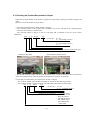
Problem Analysis Using a Personal Computer
4.7.1
Connecting a computer
(1)
Set the module in accordance with Chapter 4.4.
(2)
Connect the RS-232C terminal of the computer to the RS-232C terminal of the interface board.
(3)
Turn on the main power to the interface board. (Red LED goes on.)
POWER indicator (red LED)
4.7.2
Preparing a computer
(1)
Turn on the main power to the computer.
(2)
Set the PDPgo switch on the interface board to ON and turn on the main power to the module.
(3)
For computer running DOS/V:
C : \ > FHPH2<ENTER>
For computer running WINDOWS:
Start menu → Run → FHPH2<ENTER>
(4)
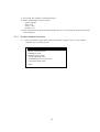
The following menu screen appears.
32H2
Main menu
<Rev. SVH2E 1.0>
** Module information menu
POWER ON menu
Problem analysis menu
Voltage adjustment menu
Accumulated power-on time menu
Logic board change menu
EXIT
-45-
*1: Use COM1: the computer's communication port.
*2: Set the communication setup as follows.
Speed: 9600 bps
Data: 7 bits
Parity: 1 none
Stop bit: 1 bit
*3: If the program starts up while the module standby power is not yet turned on, the menu screen will
not be displayed.
4.7.3
Problem Analysis Procedure
(1)
Select the problem analysis menu from the main menu using the ↑ key or ↓ key and press
<ENTER> key to start the program.
32H2
Main menu
<Rev. SVH2E 1.0>
Module information menu
POWER ON menu
** Problem analysis menu
Voltage adjustment menu
Accumulated power-on time menu
Logic board change menu
EXIT
-46-
(2) Check the error code (hexadecimal number) from the Latest error code read-out menu and locate the
faulty position from the following table.
32H2
Problem analysis menu
**_Condition code
Latest error code
Previous error Code
2nd previous error code
3rd previous error code
4th previous error code
5th previous error code
6th previous error code
7th previous error code
8th previous error code
9th previous error code
10th previous error code
11th previous error code
12th previous error code
13th previous error code
14th previous error code
15th previous error code
Error code clear / execute
:**
:**
:**
:**
:**
:**
:**
:**
:**
:**
:**
:**
:**
:**
:**
:**
:**
(Hex)
(Hex)
(Hex)
(Hex)
(Hex)
(Hex)
(Hex)
(Hex)
(Hex)
(Hex)
(Hex)
(Hex)
(Hex)
(Hex)
(Hex)
(Hex)
(Hex)
モジュールの状態
The state of the module is shown.
を示します。
最新のエラーコー
The latest error code is shown.
ドを示します。
過去のエラーコー
A past error code is shown in new
ドを新しい順に示
します。
the order.
全エラーコードを
All error code is cleared to 0.
0クリアします。
RETURN
EXIT
故障解析メニューの表示例
Example of displaying breakdown analysis menu
(3)
Select RETURN using the ↑ key or ↓ key and press <ENTER> key to start the program, then the
screen returns to the menu screen.
*
When EXIT is selected, the screen returns to the WINDOWS or DOS screen.
-47-
Error code table
ERR Detect
code position
(board)
00
LOGIC
02
LOGIC
Suspected faulty board
(In the order of higher probability of defect)
Contents
(1)
STANDBY power is stopped
(2)
Waveform ROM data error
LOGIC
LOGIC
PSU
06
3.3V power startup is faulty
X-SUS
Y-SUS
18
Internal I2C_SCL1_LOW level
LOGIC
19
Internal I2C_ACK does not respond
LOGIC
LOGIC
1C
EEPROM initial setting is defective
1D
EEPROM write-down is defective
LOGIC
1E
EEPROM user initial setting is defective
LOGIC
X-SUS
25
EEPROM factory setting reading is defective
LOGIC
Vex power voltage has decreased
X-SUS
Vex power voltage is excessive
X-SUS
ADM1 - 8 PSU
LOGIC
26
Vex power startup is faulty.
X-SUS
LOGIC
28
Vx power voltage has dropped
X-SUS
LOGIC
29
Vx power voltage is excessive
X-SUS
2A
Vx power startup is faulty.
X-SUS
LOGIC
2C
Vpx voltage has dropped
X-SUS
LOGIC
2D
Vpx voltage is excessive
X-SUS
LOGIC
30
Vpx1 voltage has dropped
X-SUS
LOGIC
31
Vpx1 voltage is excessive
X-SUS
LOGIC
34
Vpx2 voltage has dropped
X-SUS
LOGIC
35
Vpx2 voltage is excessive
X-SUS
LOGIC
39
Vs power current is excessive (during operation) X-SUS
Panel
LOGIC
3B
Vs power current is excessive (during startup)
X-SUS
Panel
LOGIC
Vey power voltage has dropped
Y-SUS
LOGIC
Vey power voltage is excessive
Y-SUS
44
Y-SUS
45
46
Vey power startup is faulty.
Y-SUS
LOGIC
4C
Vpy voltage has dropped
Y-SUS
LOGIC
4D
Vpy voltage is excessive
Y-SUS
LOGIC
50
Vpy1 voltage has dropped
Y-SUS
LOGIC
51
Vpy1 voltage is excessive
Y-SUS
LOGIC
54
Vpy2 voltage has dropped
Y-SUS
LOGIC
55
Vpy2 voltage is excessive
Y-SUS
LOGIC
59
Vs power current is excessive (during operation) Y-SUS
Panel
LOGIC
5B
Vs power current is excessive (during startup)
Y-SUS
Panel
LOGIC
Vs power current is excessive (during operation) Y-SUS
SDM
Panel
LOGIC
Vs power voltage is excessive
LOGIC
LOGIC
5D
61
PSU
62
64
65
X-SUS
Y-SUS
66
68
X-SUS
69
6A
6C
6D
X-SUS
Y-SUS
(5)
(6)
(7)
PSU temperature has
probably increased
【UA-7x】
3.3V power voltage has dropped
24
(4)
PSU
04
1F
(3)
Remarks
PSU
Vs power startup is faulty.
X-SUS
Y-SUS
PSU
Vex and Vpy power voltage has dropped
LOGIC
X-SUS
Y-SUS
Vex and Vey power voltage is excessive
X-SUS
Y-SUS
Vex and Vey power startup is faulty.
LOGIC
X-SUS
Y-SUS
Vw power voltage has dropped
Y-SUS
X-SUS
LOGIC
Vw power voltage is excessive
X-SUS
Vw power startup is faulty.
Y-SUS
X-SUS
LOGIC
Vpx and Vpy voltage has dropped
LOGIC
X-SUS
Y-SUS
Vpx and Vpy voltage is excessive
LOGIC
X-SUS
Y-SUS
-48-
ABUS-L ABUS-R LOGIC
ERR Detect
code position
( board)
81
PSU
Contents
Remarks
Suspected faulty board
(In the order of higher probability of defect)
(1)
(2)
(3)
(4)
(5)
Va power voltage is excessive
PSU
82
Va power startup is faulty.
ADM1 - 8 PSU
99
Va power current is excessive (during operation) ADM1 - 8 ABUS-L ABUS-R PSU
LOGIC
9B
Va power current is excessive (during startup)
ADM1 - 8 ABUS-L ABUS-R PSU
LOGIC
9D
Va power current is excessive (during operation) ADM1 - 8 ABUS-L ABUS-R PSU
LOGIC
(6)
(7)
LOGIC
LOGIC
A5
ADM1
ADM1 has abnormal heat generation.
ADM1
PSU
A9
ADM2
ADM2 has abnormal heat generation.
ADM2
PSU
LOGIC
AD
ADM3
ADM3 has abnormal heat generation.
ADM3
PSU
LOGIC
B1
ADM4
ADM4 has abnormal heat generation.
ADM4
PSU
LOGIC
B5
ADM5
ADM5 has abnormal heat generation.
ADM5
PSU
LOGIC
B9
ADM6
ADM6 has abnormal heat generation.
ADM6
PSU
LOGIC
BD
ADM7
ADM7 has abnormal heat generation.
ADM7
PSU
LOGIC
C5
ADM8
ADM8 has abnormal heat generation.
ADM8
PSU
LOGIC
E2
LOGIC
5V power startup is faulty.
X-SUS
Y-SUS
PANEL
E2
PSU
Detection error of Vs and Va voltage.
PSU
LOGIC
-49-
ABUS-L ABUS-R
LOGIC
PSU ABUS-L ABUS-R LOGIC
Excess current is
detected in ACCC
operation.
It can possibly occur
depending on screen
display.
5. Disassembling and Reassembling
Unless otherwise specified, use the torque screwdriver for screw tightening, following the
tightening torques below.
Screw size
Tightening torque
M3
0.69 ±0.049Nm (7±0.5kg·cm)
M4
1.18 ±0.098Nm (12 ±1.0kg·cm)
5.1 Disassembling Overview
*
*
*
The encircled numbers indicate the item numbers of the constituent parts described in item 7.
*: Power supply (jig)
-50-
5.2
Note
X-SUS Circuit Board Removal/Installation Procedure
When removing the circuit board after the main power is turned on/off, wait for at least one minute
before starting to remove the circuit board.
If the circuit board removal is started immediately after turning off the main power, it can result in
electric shock or damage to the circuit due to residual electric charge.
Remove the circuit board following the steps below. To install the circuit board, reverse the removal
procedure.
(1)
(1)XBB clamping×4
This is picked up
by the finger.
(2)
(3)
(4)
Pull off the BUS-XU/XD horizontally. Disconnect the connectors (CN24, CN25).
Release the lock of the FPC connector (CN21) and disconnect the signal cable.
Disconnect the cables from the VH connectors (CN22, CN23).
(2)CN25
Pull off
(4)CN22
(2)CN24
(4)CN23
Pull off
(3)CN21
51-
Note
* On handling the FPC connector
To release the lock, release it by gently flipping it
with the nail of the thumb or forefinger.
Never pinch the lock lever with fingers or hook on
it (especially with a fingernail). Doing so might
damage the lock lever.
(5)
Remove the fixing screws (M3×6) at the 8 locations.
(6)
Remove the X-SUS board.
52-
5.3
Y-SUS Circuit Board Removal/Installation Procedure
When removing the circuit board after the main power is turned on/off, wait for at least one minute
before starting to remove the circuit board.
If the circuit board removal is started immediately after turning off the main power, it can result in
electric shock or damage to the circuit due to residual electric charge.
Remove the circuit board by following the steps below. To install the circuit board, reverse the removal
procedure.
(1)
Remove the screws (M3X6) fixing SDM (4 locations).
(2)
Pull out the SMD horizontally and disconnect the connectors (CN34, CN35).
(3)
Release the lock of the FPC connector (CN31) and disconnect the signal cable.
(4)
Disconnect the cables from the VH connectors (CN32, CN33).
Note
(4)CN32
(2)CN35
Pull off
(4)CN33
(3)CN31
(2)CN34
Pull off
(1)screw*2
Note
* On handling the FPC connector
To release the lock, release it by gently flipping it
with the nail of the thumb or forefinger.
Never pinch the lock lever with fingers or hook
onto it (especially with fingernails). Doing so
might damage the lock lever.
-53-
(5)
Remove the fixing screws (M3×6) at 6 locations.
(6)
Remove the Y-SUS board.
-54-
5.4
ABUS-L Circuit Board Removal/Installation Procedure
Note
When removing the circuit board after the main power is turned on/off, wait for at least one minute
before starting to remove the circuit board.
If the circuit board removal is started immediately after turning off the main power, it can result in
electric shock or damage of the circuit due to residual electric charge.
Remove the circuit board by following the steps below. To install the circuit board, reverse the removal
procedure.
(1)
Disconnect the connector CN52 from the ABUS-L board.
(2)
Raise the lock of the FPC connectors CN53, CN54, CN55 to release it and remove the ADM
flexible board.
(3)
Release the lock of the FPC connector CN51 and disconnect the signal cable (FPC).
(1)CN52
(3)CN51
(2)CN54
(2)CN53
Note
* On handling the FPC connector
To release the lock, release it by pulling up the
lever.
Never pinch the lock lever with the fingers or push
hard on it without a cable in it. Doing so might
damage the lock lever.
-55-
(2)CN55
(4)
Remove the screws (M3X6) fixing the ABUS-L board at the 2 locations.
(5)
Remove the ABUS-L board.
-56-
5.5
ABUS-R Circuit Board Removal/Installation Procedure
Note
When removing the circuit board after the main power is turned on/off, wait for at least one minute before
starting to remove the circuit board.
If the circuit board removal is started immediately after turning off the main power, it can result in electric
shock or damage of the circuit due to residual electric charge.
Remove the circuit board by following the steps below. To install the circuit board, reverse the removal
procedure.
(1)
Disconnect the connector CN42 on the ABUS-R board.
(2)
Raise the lock of the FPC connectors CN43, CN44, CN45, CN46 to release it and disconnect the
ADM flexible board.
(3)
Release the lock of the FPC connector CN41 and disconnect the signal cable (FPC).
(3)CN41
(1)CN42
(2)CN43
(2)CN44
Note
* On handling the FPC connector
To release the lock, release it by pulling up the
lever.
Never pinch the lock lever with the fingers or
push hard on it without a cable in it. Doing so
might damage the lock lever.
-57-
(2)CN45
(2)CN46
(4)
Remove the screws (M3×8) fixing the ABUS-R board at in position at 2 locations.
(5)
Remove the ABUS-R board.
-58-
5.6
LOGIC Board Removal/Installation Procedure
Remove the circuit board by following the steps below. To install the circuit board, reverse the
removal procedure.
(1)
Disconnect the EH connector CN6.
(2)
Release the lock of the FPC connectors CN2, CN3, CN4, CN5 and disconnect the signal
cable (FPC).
(3)
Slide the lock of the FPC connector CN7 toward the PSU board side, then press it down
toward the front and remove the PSU signal cable.
(1)CN6
(3)CN7
(2)CN3
(2)CN2
(2)CN5
Note
* On handling the FPC connector
To release the lock, release it by gently flipping it.
Never pinch the lock lever with the fingers or
hook onto it (especially with fingernails). Doing
so might damage the lock lever.
-59-
(2)CN4
(4)
Remove the screws (M3×6) fixing the LOGIC board in position at 2 locations.
(5)
Remove the LOGIC board.
(6) Tabs for fixing
(6)
When installing the LOGIC board, place it so that the LOGIC board is locked by the tabs for
fixing it in position (at 3 locations).
-60-
5.7 PSU Board (jig) Removal/Installation Procedure
Note
When removing the circuit board after the main power is turned on/off, wait for at least one minute before
starting to remove the circuit board.
If the circuit board removal is started immediately after turning off the main power, it can result in electric
shock or damage to the circuit due to residual electric charge.
Remove the circuit board by following the steps below. To install the circuit board, reverse the removal
procedure.
(1) Release the lock of the cable clamp (large) .(At 4 locations)
(2) Disconnect the X-SUS board connector CN23.
(3) Disconnect the Y-SUS board connector CN33.
(4) Disconnect the ABUSR board connector CN42.
(5) Disconnect the ABUSL board connector CN52.
(6) Remove the wires (4), (5) from the cable clamp (small) .
(7) Disconnect the LOGIC board connector CN6.
(8) Disconnect the PSU signal cable from the PSU board connector CN69 side.
(8) CN69
(3) CN33
(2) CN23
(7) CN6
(1) Cable bind (4 points)
(5) CN52
(6) Cable bind (2 points)
-61-
(4) CN42
(9)
Remove the screws (M3×6) fixing the PSU board in position. (7 locations)
(10)
Use cutting pliers to cut the nylon bands tying the following 5 power cables.
(11)
・CN64 (PSU) ~ CN32 (Y-SUS)
:
・CN65 (PSU) ~ CN23 (X-SUS)
:
・CN66 (PSU) ~ CN42 (ABUSR)
:
・CN67 (PSU) ~ CN52 (ABUSL)
:
・CN22 (X-SUS) ~ CN23 (Y-SUS)
:
Remove the PSU board.
-62-
(12)
When the installation of the board is complete, route the wires as shown below.
Pass the CN52 cable (RED/ BLK/ GRY)
under the signal cable.
Route it on top of the PSU signal cable.
Pass the CN42 cable (YEL/BLK/GRY)
under the signal cable.
Enlarged
CN63
CN63
Wrap the CN23 cable (YEL/BLK/GRY) around the other
cables (4 types) coming from the PSU board by one full turn
and then insert CN23 into the X-SUS board. (Note that the
cable must not touch the PSU board CN63.)
-63-
5.8
Panel Chassis Replacement Procedure
(1)
Remove the 6 types of printed-circuit board (X-SUS, Y-SUS, ABUSL, ABUSR, LOGIC,
and PSU) that are installed in the panel module.
For the removal procedure, refer to Section 5.2 to 5.7.
*
(2)
Before removing the above 6 types of board, be sure to remove both ends of the single
power cable (BLU) and those of the four FPC cables (WHT) that are used to connect the
circuit boards.
Remove the rivets fixing the complete panel chassis (maintenance part) and XBB board in
position (4 locations).
*
The removed rivets are used only for keeping the machine from shifting during
transportation, and are not used for the product.
R iv e t ( P C B su p p o r t) x 4 p c s
C h a s s is
P anel
(3)
Install panel chassis (repair parts) the printed-circuit board that was removed in step (1) and
fix it in position. (Refer to the exploded view shown in Section 5.1.)
(4)
Print the serial ID number of the product to be repaired on the product label, which is
prepared separately. Attach the product label to the panel chassis on top of the X-SUS board
(See the photo)
-64-
6
Operation Check and Adjustment Method
6.1
List of Check and Adjustment Items
Adjustment position
Adjustment item
(Major item)
VR adjustment
Parameter
adjustment
Adjustment item
(Minor item)
(Name of the part)
Is detection adjustment
Ve voltage adjustment
Vw voltage adjustment
Vx voltage adjustment
CU timing adjustment
CD timing adjustment
LU timing adjustment
LD timing adjustment
Ve voltage adjustment
Is detection adjustment
CU timing adjustment
CD timing adjustment
LU timing adjustment
LD timing adjustment
PFC voltage
adjustment
Vs adj1
Vs adj2
Va adj2
Vs f min
Vpr adj
Vcc f min
Vcc adj
Va adj1
Vaa
Va f min
Vs voltage adjustment
Va voltage adjustment
Vw voltage adjustment
Vx voltage adjustment
X-SUS board RE1
X-SUS board RE108
X-SUS sub-board R10
X-SUS sub-board R39
X-SUS sub-board VR1
X-SUS sub-board VR2
X-SUS sub-board VR3
X-SUS sub-board VR4
Y-SUS board RY75
Y-SUS board RE1Y
Y-SUS sub-board VR1
Y-SUS sub-board VR2
Y-SUS sub-board VR3
Y-SUS sub-board VR4
PSU board RV301
Error history clear
Default setting
Accumulated power-on
time clear
PSU board RV801
PSU board RV802
PSU board RV803
PSU board RV901
PSU sub-board RV201
PSU sub-board RV150
PSU sub-board RV270
PSU sub-board RV860
PSU sub-board RV861
PSU sub-board RV950
LOGIC board(Vsvolt)
LOGIC board(Vavolt)
LOGIC board(Vwvolt)
LOGIC board(Vxvolt)
LOGIC board
(EEPROM)
LOGIC board
(EEPROM)
Check and adjustment
When PDP
panel is
replaced
When
X-SUS
board is
replaced
When
Y-SUS
board
is replaced
Required timing
When
LOGIC
board
is replaced
When ABUS
board
is replaced
Labor
When PSU
board
is replaced
Jig/tools
Digital voltmeter ,
screwdriver
Be sure to keep the default setup set at the factory.
(Do not change the VR control settings.)
{
{
{
{
{
{
{
{
{
{
{
{
{ : Check, adjustment, or setup
-65 -
{
Interface board,
personal
computer, Digital
voltmeter
{
required
Interface board,
personal computer
Labor
(persons)
Time
(minutes)
1
1
1
1
1
1
1
1
1
1
1
1
1
1
1
1
1
1
1
1
1
1
1
1
1
1
1
1
1
1
1
1
1
1
1
1
1
1
1
1
1
1
1
1
1
1
1
1
1
1
1
1
1
1
1
1
1
1
1
1
1
1
6.2
Check and Adjustment Method
6.2.1
Check and adjustment procedure
Check and adjustment
Was LOGIC board
replaced?
Y
Logic board data transfer
(Section 6.2.5)
N
Y
Was Panel chassis
replaced? replaced?
Parameter adjustment
(Section 6.2.2)
N
Operation/performance check
(Section 6.2.3)
No abnormality?
N
Y
Burn-in mode setting
(Section 6.2.4)
Heat run
(Section 6.2.4)
Y
Abnormal
N
Was Panel chassis
Accumulated power-on time
reset
(Section 6.2.6)
Y
replaced?
N
Default setup (Error history clear)
(Section 6.2.7)
Re-analysis
To Section 4.2
End
-66-
6.2.2 Glass Panel Driving Voltage Adjustment (Voltage Data Loading)
List of parameter adjustment items
Ite
m
1
Adjustment items
Vs voltage
adjustment
Adjustment parameter
Measurement point
Vrs
Adjustment value
(conditions)
PSU board TP5
Voltage setting label
indication value*
±1%
2
Va voltage
adjustment
Vra
PSU board TP4
Voltage setting label
indication value*
±1%
3
4
Vw voltage
adjustment
Vx voltage
adjustment
Vrw
Vrx
(all black)
(all black)
X-SUS board
connector
Voltage setting label
indication value*
CNX01 6-pin
±1%
X-SUS board
connector
Voltage setting label
indication value*
CNX01 1-pin
±1%
(all black)
(all black)
*: Voltage setting label shows the following messages at the top left of the back of the chassis.
< LOT >
Vs =
Vw =
.
.
V
V
Va =
Vx =
.
.
V
V
<X-SUS Board>
<Y-SUS Board>
PVS(VS)
<PSU Board>
PVX(VX)
PVW(VW)
PGND(GND)
PVA(VA)
<LOGIC Board>
<ABUSL Board>
<ABUSR Board>
-67-
Remarks
(1)
From the main menu, select the voltage adjustment menu with the ↑key or ↓key and press the
<ENTER> key.
32H2 Main menu
Module information menu
Power ON menu
Problem analysis menu
** Voltage adjustment menu
Accumulated power-on time menu
Logic board change menu
EXIT
(2)
From the voltage adjustment menu, adjust parameters in the order starting from Vs, Va, Vw, and Vx.
Select parameter with the ↑key or ↓key and adjust the parameter with the →key (increment) or ←key
(decrement). The adjustment values are shown on the voltage label that is attached to the panel chassis.
32H2 Voltage adjustment menu
** Voltage adjustment / Vs[V] : **.**
Voltage adjustment / Va[V] : **.**
Voltage adjustment / Vw[V] : **.**
Voltage adjustment / Vx[V] : ***.**
RETURN
EXIT
** numbers are shown in decimal values.
Input the numeric value/dot and press the <ENTER> key and then press the <ENTER>
key again to set the adjustment value directly.
(3)
Select RETURN with the ↑key or ↓key and press the <ENTER> key to return to the menu screen.
-68-
6.2.3
Operation performance check items
(1)
Environmental conditions
Temperature: Room temperature
Judgment distance: 1 meter from panel screen
Preheat run: 5 minutes with entire screen lit (white)
(2)
Test patterns:
PSEL
H
H
H
H
H
H
H
H
L
L
L
L
L
L
L
L
Push
SW
0
1
2
3
4
5
6
7
0
1
2
3
4
5
6
7
Display pattern
Size
Details
White screen
Cross slash
Vertical stripe
Horizontal stripe
Color bars
Gray scale
Color gray scale
Divided WINDOW
1% WINDOW
Cross slash
Vertical stripe
Horizontal stripe
Color bars
Gray scale
Color gray scale
Divided WINDOW
Large
Every other dot
Every other line
Vertical bar
Horiz. direction
Horiz. direction
9 blocks
Center
Small
Every other cell
Every 2 lines
Horizontal bar
Vert. direction
Vert. direction
16 blocks
24 ×24
H_blk divided in 8
Every 3 dots
Every 3 dots
Follow the ROM
Follow the ROM
12 ×12
V_blk divided in 8
Every 4 dots
Every 4 dots *2
Follow ROM *3
PDPGO SW
CPUGO SW
-69-
(3)
Judgment
Item
1
2
Test items
Brightness
Test signal
Judgment criterion
White screen (W)
Brightness non-uniformity in the form of stripes
non-uniform
must not be visible in vertical and horizontal
ity
directions.
Black noise
Horizontal gray scale
(Each color of R/G/B)
3
4
5
Rank 3 or higher in the 5-step evaluation.
<Rank>
5: No noise
4: Small noise is intermittently visible
3: Noise of 1 line is not visible continuously
2: Noise occurs continuously
1: Much noise occurs continuously
Number of
The entire screen lights
Conforms to Section 1.3.2 Display quality
defects
(Each color of
specifications.
Number of
W/R/G/B)
However, when Delivery Specifications Sheets are
extra dots
prepared for each client, the specifications shown in
Number of
the Delivery Specifications Sheet must be met.
flickering
dots
(4) Power ON/OFF
・ Power ON
Both PDPGO-SW and CPUGO-SW are made set of turning on.
・ Power OFF
Only PDPGO-SW is made set of turning off.
(CPUGO-SW is in the state of turning on.)
-70-
6.2.4
Heat Run Test
(1)
Set the module by following the same procedure as that for Problem Analysis in Section 4.7.
(2)
From the main menu, select the POWER ON menu with the ↑key or ↓key and press the <ENTER>
key.
32H2 Main menu
Module information menu
** Power ON menu
Problem analysis menu
Voltage adjustment menu
Accumulated power-on time menu
Logic board change menu
EXIT
(3)
From the POWER ON menu, select the Module power with the ↑key or ↓key and press the <ENTER>
key. When you press the →key, the main power of the module is turned on. (When you press the ←key,
the main power is turned off.)
32H2 Power ON menu
** Internal pattern selection :**
00 - changing colors (full picture)
01 - blue
02 - green or red
03 - syan or magenta
04 - red or green
05 - magenta or syan
06 - yellow
07 - white
08 - black
10 - factory pattern (OLD)
77 - factory pattern
Burn–in start / execute
RETURN
EXIT
(4) To change the internal pattern, select the internal pattern selection from the POWER ON menu using the ↑
(up) or ↓(down) key, and press the <ENTER> key.
Setup
value
00
01
02
03
04
(5)
Display pattern
01 to 08 patterns are displayed
every 2 seconds.
Entire screen is blue
Entire screen is red
Entire screen is magenta
Entire screen is green
Setup
value
05
Display pattern
Entire screen is cyan
06
07
08
09
Entire screen is yellow
Entire screen is white
Entire screen is black
Plant burn-in pattern
From the POWER ON menu, select Burn-in start with the ↑key or↓key and press the <ENTER> key.
The display pattern is automatically generated in PDP.
(6)
Select RETURN with ↑key or↓key and press <ENTER> key to return to the menu screen
-71-
6.2.5
Logic board parameter forwarding
(1) The module is set according to the same to failure analysis procedure in clause 4.7.
The logic board before being exchanged is installed in the module.
(2) From the main menu, select change Logic board menu with the ↑key or ↓key and press the <ENTER> key.
32H2 Main menu
Module information menu
** Power ON menu
Problem analysis menu
Voltage adjustment menu
Accumulated power-on time menu
Logic board change menu
EXIT
(3) From the logic board change menu, select data copy with the ↑key or ↓key and press the <ENTER> key.
Data is read before the Logic board is exchanged.
32H2 Logic board change menu
** Data copy (PDP -> Temp.FILE)/execute
Data Paste (PDP -> Temp.FILE)/execute
RETURN
EXIT
(4) The Logic board is exchanged.
(6) From the logic board change menu, select data paste with the↑key or ↓key and press the<ENTER> key. Data
is written in the exchanged Logic board.
32H2 Logic board change menu
Data copy (PDP -> Temp.FILE)/execute
** Data Paste (PDP -> Temp.FILE)/execute
RETURN
EXIT
(6) Select RETURN with ↑key or ↓key and press <ENTER> key to return to the menu screen.
-72-
6.2.6 Accumulation time reset
(1) The module is set according to the same to failure analysis procedure in clause 4.7.
(2) From the main menu, select Power-on time menu with the ↑key or ↓key and press the <ENTER> key.
32H2 Main menu
Module information menu
Power ON menu
Problem analysis menu
Voltage adjustment menu
** Accumulated power-on time menu
Logic board change menu
EXIT
(3) From the Power-on time menu, select Operation hours with the ↑key or ↓key and press the <ENTER> key.
The Operation hour is input. *It is not possible to change in the energizing time according to the version of the
service software.
32H2 Accumulated power-on time menu
** Running time indication:[hh:mm:ss]=
RETURN
EXIT
(4) "minute" is continuously input and < ENTER > key is pushed.
(5) "Second" is continuously input and < ENTER > key is pushed.
(6) Select RETURN with ↑key or ↓key and press <ENTER> key to return to the menu screen.
-73-
6.2.7
Setup Before Shipment
Before shipment from Service Center, perform the following setup or initialization.
1) Initial values that are shown in the List of EEPROM contents in Section 3.3.1.
(Main power of the module is turned off.)
2)
Clearing the error codes
(1)
From the main menu, select the Shipment from service setting/execute with the ↑key or↓ key and press
the <ENTER> key.
(2)
Shipping the set screen is displayed, and “Y" is pushed.
In shipping the set processing, there is a thing that the power supply of the module turns on
automatically.
The shipment setting ends, and when the power supply of the module is on, the power supply is turned
off automatically.
Shipment from service setting?(input the "Y" or "N" key)
“N" When the key is pushed, the shipment setting is not done, and the power supply is turned off.
-74-
7. The parts information
Model name
Module name
Parts No.
KE-32TS2
FPF32C106128UA-73
9-885-048-69
FPF17R-XSS5016 BOARD
2
9-885-048-70
FPF17R-YSS5017 BOARD
3
9-885-048-71
FPF17R-LGC5018 BOARD
4
9-885-048-72
FPF17R-ABR5015 BOARD
5
9-885-048-73
FPF17R-ABUL5014 BOARD
6
9-885-053-30
FPF32C106128UA-73
1
Parts name
-75-
Others
9-878-210-01
Sony EMCS Corporation
Ichinomiya TEC
2003LL08-Data
Made in Japan
2003. 12