1
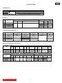
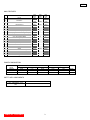
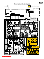
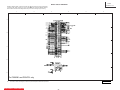
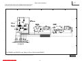
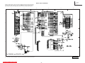
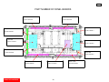
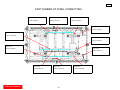
No. 0226
PA
P50X901/DW3D
P50V701/DW3D
P50S601/DW3F
SERVICE MANUAL
NTTSSCC
N
NTTSSCC
A
P
D
D W1
3
AC h a s s i s
R/C: CLU-4372A / CLU-123S P50X901
R/C: CLU-4374A
P50V701
R/C: CLU-4373A
P50S601
PRELIMINARY
This ADDENDUM is made due to the new models P50X901 (DW3D), P50V701 (DW3D) and P50S601 (DW3F).
They are different to models P50H401 (DW3A), P50T501 (DW3A) and P50H4011 (DW3A). The Main difference is the
panel, the X/V/S models use "AF1" Plasma Panel and the H/T Models use "AE1" Plasma Panel. Software (Digital Main PWB)
is also different because of Plasma Panel difference.
Refer to Service Manual PA0224 when servicing X/V/S models in regards to other adjustments not covered in this addendum.
This ADDENDUM indicates only the differences and special considerations to be taken when servicing the X/V/S models.
CONTENTS
SPECIFICATIONS . . . . . . . . . . . . . . . . . . . . . . . . . . . . . . . . . . . . . . . . . . . . . . . . . . . . 2
ADJUSTMENTS . . . . . . . . . . . . . . . . . . . . . . . . . . . . . . . . . . . . . . . . . . . . . . . . . . . . . . . 4
BLOCK DIAGRAM . . . . . . . . . . . . . . . . . . . . . . . . . . . . . . . . . . . . . . . . . . . . . . . . . . . . . 5
CONNECTION DIAGRAM . . . . . . . . . . . . . . . . . . . . . . . . . . . . . . . . . . . . . . . . . . . . . . . 7
FINAL WIRING DIAGRAM . . . . . . . . . . . . . . . . . . . . . . . . . . . . . . . . . . . . . . . . . . . . . . . 9
QUICK DISASSEMBLY GUIDE . . . . . . . . . . . . . . . . . . . . . . . . . . . . . . . . . . . . . . . 11
CIRCUIT SCHEMATIC DIAGRAMS . . . . . . . . . . . . . . . . . . . . . . . . . . . . . . . . . . . . . . . 13
PRINTED CIRCUIT BOARDS . . . . . . . . . . . . . . . . . . . . . . . . . . . . . . . . . . . . . . . . . . . . 28
PARTS LIST . . . . . . . . . . . . . . . . . . . . . . . . . . . . . . . . . . . . . . . . . . . . . . . . . . . . . . . . . . 28
PANEL PART S . . . . . . . . . . . . . . . . . . . . . . . . . . . . . . . . . . . . . . . . . . . . . . . . . . . . . . . 29
QUICK REFERENCE PARTS LIST . . . . . . . . . . . . . . . . . . . . . . . . . . . . . . . . . . . . . . . . 49
CAUTION:
These servicing instructions are for use by qualified service personnel only. To reduce the risk of
electric shock do not perform any servicing other than that contained in the operating instructions
unless you are qualified to do so. Before servicing this chassis, it is important that technician
read the “IMPORTANT SAFETY INSTRUCTIONS” in Service Manual PA0224.
SAFETY NOTICE
USE ISOLATION TRANSFORMER WHEN SERVICING
Components having special safety characteristics are identified by a ! on the schematics and on the parts list in this
Service Manual and on the PA0224. Before servicing the chassis, it is important that the service technician read and
follow the “Important Safety Instructions” shown in Service Manual PA0224.
SPECIFICATIONS AND PARTS ARE SUBJECT TO CHANGE FOR IMPROVEMENT
PLASMA DISPLAY PANEL
MAY 2007
HHEA-MANUFACTURING DIVISION
DW3
SPECIFICATIONS
APPEARANCE
Model name
P50X901
P50S601
P50V701
Series Name
Director's
UltraVision
UltraVision
Cabinet Design
High Gloss Black/Frame, High Gloss Black/Bezel, High Gloss Hidden/SP
High Gloss Black/Frame, Black/Bezel, High Gloss Hidden/SP
High Gloss Black/Frame, Black/Bezel, High Gloss Hidden/SP
SYSTEM
No.
Model name
VHF(ch)
1
2
3
P50X901
P50S601
P50V701
2~13
Channel coverage band
UHF(ch)
CATV(ch)
14~69
A-5~A-1, A~I,J~W,W+1~W+94
Reception system
NTSC
ATSC
64QAM/
(8VSB) 256QAM
X
X
X
X
X
X
X
X
X
STRUCTURAL DIMENSIONS
No.
Model name
WIDTH
[mm]
HEIGHT
[mm]
DEPTH
[mm]
WEIGHT
[kg]
1
P50X901
1250
885(817)
423(134)
50.9(44.8)
2
3
P50S601
P50V701
1241.4
1241.4
884(820.2)
884(820.2)
422.7(129)
422.7(129)
49.8(43.7)
49.9(43.8)
Note
Without table
top stand.
EXTERNAL TERMINALS AND JACKS
Model
name
P50X901
P50S601
P50V701
Model
name
P50X901
P50S601
P50V701
Rear
A/V
IN
3
3
3
Front
A/V
IN
1
1
1
S
IN
1
1
1
S
IN
-
-
-
COMP.
IN
2
2
2
COMP.
IN
-
-
-
TABLE OF CONTENTS
HDMI
2
2
2
HDMI
1
1
1
M
OUT
1
1
1
Photo
(SD)
1
1
1
A
OUT
1
1
1
Subwoofer
OUT
-
-
-
Upgrade
←Common
←Common
←Common
2
DV
IN
-
-
-
ANT
IN
1
1
1
Rear
IR OUT
1
-
1
OPT
OUT
1
1
1
IR OUT
/G-LINK
1
(1: Service)
1
DV IN
IEEE 1394
-
-
-
POD
CARD
1
-
1
SWIVEL
OUT
1
1
1
RS232C
1
1
1
DW3
MAIN FEATURES
No.
Feature
1
Panel
2
Resolution
3
4
5
6
7
8
9
10
11
12
13
14
15
16
17
18
19
20
21
Front Filter with ARF
(Transparency)
Seine2
FRC (FC8)
One NTSC/ATSC Tuner
POD (Point Of Deployment)
PinP (Digital/External Analog SPLIT)
3 Picture Mode
Color Temperature Mode
Color Decoding Adjustment
Color Management Adjustment
7 Mode Aspect Ratio Interchangeable
EPG (G-GUIDE) Function
SD-card Photo Viewer
Audio Output
Swivel
AV NET, AV NET Learning
IR Pass Through
OSD Design
Energy Star
P50
X901
AF1
1920x
1080i
Mesh
(36%)
X
X
X
X
X
X
4
X
X
X
X
X
10W x2
Power
X
X
Direc.
-
P50
S601
AF1
1920x
1080i
Mesh
(41%)
X
-
X
-
-
X
4
-
-
X
-
-
10W x2
Power
-
-
B
-
P50
V701
AF1
1920x
1080i
Mesh
(36%)
X
X
X
X
X
X
4
-
-
X
X
X
10W x2
Power
X
X
C
-
POWER CONSUMPTION
MODEL
NAME
P50X901
P50S601
P50V701
INDICATED
Max. Rating
605W
587W
605W
VALUE
Max. Rating
5.7A
5.3A
5.7A
(Average Rating)
364W
350W
364W
SAFETY KEY COMPONENTS
Symbol.No. / P/N / Spec.
F9A1 / P#FN00551 / Fuse
10A
TABLE OF CONTENTS
Model
P50X901, P50V701, P50S601
3
PST
Without POD
0.6W
0.6W
0.6W
[W]
CHASSIS
With POD
14W
14W
DW3D
DW3F
DW3D
DW3
ADJUSTMENTS
NOTE: The next adjustment procedure is only for the P50X901, P50V701 and the P50S601, refer to the service manual PA
no. 0224 for all the other adjustments.
VIDEO COLOR TEMPERATURE ADJUSTMENT - BLACK AND WHITE MODE.
-Preparation
(1) Set the output of signal generator to white raster (Ratio: 100%).
(2) Component signal (480i)
Video level:
0.7Vp-p
SYNC:
0.3Vp-p
Set-up level:
0V
(3) Input white raster signal into COMPONENT input terminal.
(4) Set user control to Day (Dynamic) mode (Picture mode).
(5) Confirm that the mode is set as ‘Factory setting mode’.
(6) Aspect: 4:3 Expanded.
-Adjustment
(1)
(2)
(3)
(4)
Perform the following adjustment with the remote control.
Set the CRT color analyzer (CA-100) at the center of the panel.
Ensure that the adjustment parameters R/G/B DRIVE(B/W) are all set as FF.
After receiving the PC signal, reduce the value of two (or only one) of the RGB adjustment
parameters step down two (or one) among adjustment R/G/B DRIVE(B/W) and adjust the value
shown below.
Specification
Video Color temperature (B/W)
x = 0.335 ± 0.005
y = 0.343 ± 0.005
(Color temp:5400K)
At least one of the data should be FF.
-Remarks
(1) Color temperature should be adjusted under the condition in which the screen is the brightest,
thus the initial value for adjustment is set at its maximum.
(2) Adjustment is made by reducing brightness only. Reduce the brightest color for adjustment.
(3) Video color temperature & Adjustment number are the same, but addresses in the memory are
different, thus there’s no problem.
(4) When this adjustment item is done through MMC slot, Sniffer Jig must be inserted after the set is
switched to Sniffer Mode. (the PC would have trouble if this sequence is not kept.)
TABLE OF CONTENTS
4
DW3
BLOCK DIAGRAM
For P50X901, P50V701 and P50S601.
Y SUS
Scan Driver
Scan Driver
X-SUS
P50X901, P50V701 only.
Address Driver
Driver Controller
PDP
Panel
Module
LOGIC
LVDS Receiver Signal Controller
Vcego
Vsago
AC
Inlet
RGB
(LVDS)
Power
Supply
Unit
Filter PWB
Fuse
Data Controller
Main
Power SW
CPUgo
PDPgo
FAN
FAN
FAN
FAN
FC8 PWB
FC8
DDR2
DC-DC
Conv.
Main-Digital PWB
AC-CLK
Power2
Sub
Micro
PLD
(Nereid)
DC-DC
Conv.
Demodulator
Power1
POD PWB
PLD
(Oberon)
Seine2
A-chip
Seine2
D-chip
Audio
DSP
DDR2
Audio
ADC
Audio
PWM
Digital
Audio
Amplifier
Audio
DAC
VCXO
PLL
Digital/
Analog
Tuner
Video
SW
Reg.
For FAN
Audio
SW
A/V
Pin Jack
POD
Card I/F
DC-DC
(POD-Vcc)
Terminal PWB
UEI
HDMI
IR-Blaster
Driver
RS-232C
Motor
Driver
OPT-Audio
Output
Remote
Control
IR
Receiver
LED
LED PWB
Key
SW
A/V
Pin Jack
HDMI
I/F
Control PWB
SD/MMC
Card I/F
SD PWB
Speaker R
Speaker L
Stand
TABLE OF CONTENTS
5
DW3
Power system block diagram
P50X901, P50V701 only.
AC120V
PDP Panel Module
Filter PWB
Power Supply Unit
Vs
Va
Vcc
+16V
AC
SW
+15V
+10.5V
+5.6V
STBY+5V
Main-Digital PWB
+3.3V
Reg.
+12V
Reg.
Bus
SW
+5V
Reg.
+3.3V
Reg.
Digital
Audio Amp.
+9V
Reg.
Audio
DSP
Audio
PWM
+1.3V
DC-DC
Audio
DAC
+2.5V
Reg.
+3.3V
Reg.
+3.3V
Reg.
Cable
Equalizer
Key
ROM
+30V
Reg.
+3.3V
Reg.
+1.0V
DC-DC
Seine2-D
DDR2
Bus
SW
+5V
Reg.
Demodulator
+5V
Reg.
+5V
Reg.
Tuner
OOB
AV-Control
+9V
Reg.
LPF
Buffer
+5V
Reg.
AGC
I2C
Level shift
+9V
Reg.
+3.3V
Reg.
+2.5V
Reg.
Vari.
Reg.
x2
FAN
x2
FAN
IR-Blaster
Driver
Swivel
Motor
Driver
Swivel
Stand
Vari.
Reg.
PODVcc
PODVpp
POD PWB
FC8 PWB
Oberon2
+1.8V
DC-DC
+1.05V
DC-DC
x2
IR-receiver
LED
I2C
Buffer
LED PWB
TABLE OF CONTENTS
Clock
Buffer
SD PWB
SD
MMC
+1.05V
Reg.
Buffer
Control PWB
6
FC8DDR2
PLD
(Nereid)
+3.3V
DC-DC
+1.2V
Reg.
Buffer
OPT
Output
Seine2-A
Flash Memory
(OneNand)
VCXO PLL
AV SW
+3.3V
Reg.
IR
Mod.
+2.5V
Reg.
+9V
Reg.
Terminal PWB
+1.5V
Reg.
+5V
Reg.
+3.0V
Reg.
+1.8V
Reg.
Sub
MICRO
+3.3V
Reg.
+2.5V
Reg.
Seine2-D
+5V
Reg.
+3.3V
DC-DC
+1.3V
Reg.
+3.3V
Reg.
Audio
ADC
+1.8V
DC-DC
x2
+3.3V
Reg.
FC8
+1.8V
Reg.
LVDS
SW
DW3
CONNECTIONS DIAGRAM
For P50S601.
Power Supply Unit
PDP Module
CONNECTION DIAGRAM
CN64
VH-10P
AC INLET
FILTER PWB
PFAC
VT-2P
AC IN
Va
N.C.
Vcc
GND
GND
GND
N.C.
Vs
Vs
Vs
PPU1
VT-2P
CN61
VT-2P
L
2 AC(L)
AC(L)
1
1 AC(L)
N
1 AC(N)
AC(N)
2
2 AC(N)
CN23
VH-10P
1
2
3
4
5
6
7
8
9
10
1
2
3
4
5
6
7
8
9
10
CN68
PH-9P
FG
Vcc
GND
N.C.
GND
Vra
Vrs
Vcego
Vsago
N.C.
Va
N.C.
Vcc
GND
GND
GND
N.C.
Vs
Vs
Vs
CN8
PH-9P
1
2
3
4
5
6
7
8
9
1
2
3
4
5
6
7
8
9
Vcc
GND
N.C.
GND
Vra
Vrs
Vcego
Vsago
N.C.
Main Digital board
CN63
EH-8P
STBY+5V
GND
N.C.
PoWERoFF
ACCLoCK
PoWER1
PoWER2
N.C.
PPM1
ZH-08H
1
2
3
4
5
6
7
8
1
2
3
4
5
6
7
8
CNPPS
EH-15P
+5.6V
+5.6V
+5.6V
GND
GND
GND
+10.5V
GND
+16V
GND
GND
GND
+15V
+15V
+15V
EC01
FI-RE51S
STBY+5V
GND
N.C.
PoWERoFF
ACCLoCK
PoWER1
PoWER2
PNLoN
GND
SDA
SCL
GND
PNL_RX
iRQ
PNL_TX
PDWN
PNLRST
PNLoN
GND
TA1TA1+
TB1TB1+
TC1TC1+
GND(LVDS)
TCLK1TCLK1+
GND
TD1TD1+
TE1TE1+
GND
GND
TA2TA2+
TB2TB2+
TC2TC2+
GND(LVDS)
TCLK2TCLK2+
GND
TD2TD2+
TE2TE2+
GND
GND
GND
GND
GND
N.C.
PNL_MoDE
PNL_P2
PNL_P0
PNL_CLK
PPM2
DF3D-15H
1
2
3
4
5
6
7
8
9
10
11
12
13
14
15
1
2
3
4
5
6
7
8
9
10
11
12
13
14
15
+5.6V
+5.6V
+5.6V
GND
GND
GND
+10.5V
GND
+16V
GND
GND
GND
N.C.
N.C.
N.C.
PPM3
PPM2
DF3D-15H
PA-6V
1
2
3
4
5
6
GND
GND
GND
+15V
+15V
+15V
TERMINAL PWB
PSM
501497-160VS
SWIVEL PWB
PWT
52418-05HS-D
1
3
5
7
9
11
13
15
17
19
21
23
25
27
29
31
33
35
37
39
41
43
45
47
49
51
53
55
57
59
61
63
65
67
69
71
73
75
77
79
81
83
85
87
89
91
93
95
97
99
101
103
105
107
109
111
113
115
117
119
121
123
125
127
129
131
133
135
137
139
141
143
145
147
149
151
153
155
157
159
PTW
53290-05VP-D
GND
MoToR+
MoToRJoiNTDET
SW_CoM
1
2
3
4
5
VCC
LoCK
GND
1
2
3
VCC
LoCK
GND
1
2
3
1
2
3
4
5
GND
MoToR+
MoToRJoiNTDET
SW_CoM
FAN
PFA1
ZH-03H
1 VCC
2 LoCK
3 GND
FAN
PFA2
ZH-03H
1 VCC
2 LoCK
3 GND
FAN
PFB1
ZH-04H
VCC
LoCK
GND
1
2
3
VCC
LoCK
GND
1
2
3
1
2
3
4
VCC
LoCK
GND
N.C.
FAN
PFB2
ZH-04H
1
2
3
4
VCC
LoCK
GND
N.C.
GND
+5.6V
+5.6V
+5.6V
+5.6V
GND
SBY+5.0V
GND
+16V
GND
N.C.
iRoUT
N.C.
N.C.
FiN
RiN
CPDET
SWVLDET
GND
AEP_R
AEP_L
GND
ASP_R
ASP_L
GND
N.C.
GND
SEL_L_S
SEL_R_S
GND
SCL1_3V_100
SDA1_3V_100
GND
SCL_TU
SDA_TU
ANA/DIGI
GND
IF_AGC
GND
FDC_AGC
GND
FAT_INP
GND
GND
FAT_INN
GND
FDC_INP
GND
FDC_INN
GND
FS_OUTP
GND
PoWERoFF
GND
FS_OUTN
GND
GND
FAN_DET
GND
MTV_AFC
SIG_DET
N.C.
PNLoN
GND
REC_MUTE
GND
N.C.
N.C.
GND
N.C.
N.C.
N.C.
N.C.
N.C.
N.C.
N.C.
N.C.
GND
N.C.
GND
PMS1
501493-160VP
GND
D+3.3V
D+3.3V
D+3.3V
GND
GND
SBY+3.3V
GND
+10V
SWiVEL_G
MAiN_Y/V
GND
MAiN_Y_E
GND
MAiN_PB
GND
MAiN_PR/C
GND
SUB_Y/V
GND
S/PDiT
GND
SD_Yo
GND
SD_Co
GND
FAN_EN
N.C.
GND
N.C.
N.C.
GND
N.C.
N.C.
GND
SEL_L_M
SEL_R_M
GND
UATXD3
UARXD3
GND
SDA2_3V_100
GND
SCL2_3V_100
GND
N.C.
N.C.
PoWER_2_Td
N.C.
GND
FAN_CONT
N.C.
GND
N.C.
N.C.
N.C.
N.C.
GND
N.C.
GND
N.C.
GND
N.C.
GND
N.C.
GND
N.C.
GND
AVCTXD
AVCRXD
AVCCTS_N
AVCRTS_N
GND
N.C.
N.C.
N.C.
N.C.
N.C.
N.C.
N.C.
2
4
6
8
10
12
14
16
18
20
22
24
26
28
30
32
34
36
38
40
42
44
46
48
50
52
54
56
58
60
62
64
66
68
70
72
74
76
78
80
82
84
86
88
90
92
94
96
98
100
102
104
106
108
110
112
114
116
118
120
122
124
126
128
130
132
134
136
138
140
142
144
146
148
150
152
154
156
158
160
V4_CY
GND
V4_Y
GND
V4_C
GND
V4_L
V4_R
GND
T+9V
PWRKEY
ADKEY0
ADKEY1
GND
1
2
3
4
5
6
7
8
9
10
V4_CY
GND
V4_Y
GND
V4_C
GND
V4_L
V4_R
GND
T+9V
+
-
Lout-P
Lout-N
Rout-P
Rout-N
SD PWB
PSD
PDS
CNPPS
501331-12V
EH-15P
501568-12H
SDCLK
SDCMD
GND
SDDAT0
SDDAT1
SDDAT2
SDDAT3
+5.6V
SDCD
SDWP
GND
D+3.3V
VBUS
VBUS
VBUS
GND
D+
DGND
+3.3V
+5V
WP
HPD
DDCPOW
GND
SDA
SCL
ACK
GND
ClockClock+
GND
Data0Data0+
GND
Data1Data1+
GND
Data2Data2+
GND
CEC
GND
PSC
PTF
ZH-13H
GH-04H
1 PWRKEY
2 ADKEY0
3 ADKEY1
4 GND
1
2
3
4
5
6
7
8
9
10
11
Speaker (R)
+
-
LED PWB
TABLE OF CONTENTS
1
2
3
4
PDS
PSD
PPM2
501568-12H
DF3D-15H
501331-12V
1
2
3
4
5
6
7
8
9
10
11
12
P403
PH01
FIR-31V
FI-RE31S
PLS
501331-11V
iR_iN
STBY+3.3V
iR_CAPiN
GND
+5.6V
STBY+5V
ALARMLED0
PWRLED0
PWRLED1
MLEDG_N
MLEDR_N
GND
SDA
SCL
N.C.
N.C.
IRQOUT
N.C.
PDWN
CPUGO
PDPGO
GND
RA0RA0+
RA1RA1+
RA2RA2+
GND
RACLKRACLK+
GND
RA3RA3+
RA4RA4+
GND
GND
RB0RB0+
RB1RB1+
RB2RB2+
GND
RBCLKRBCLK+
GND
RB3RB3+
RB4RB4+
GND
GND
GND
GND
GND
N.C.
N.C.
N.C.
N.C.
N.C.
PSPK
PA-04V
PTC
PTF
ZH-13H
GH-10V
1
2
3
4
5
6
7
8
9
10
11
12
13
14
1
2
3
4
5
6
7
8
9
10
11
12
13
14
15
16
17
18
19
20
21
22
23
24
25
26
27
28
29
30
31
32
33
34
35
36
37
38
39
40
41
42
43
44
45
46
47
48
49
50
51
Speaker (L)
CONTROL PWB
PCST
GH-14V
CN1
FI-RE51S
51
50
49
48
47
46
45
44
43
42
41
40
39
38
37
36
35
34
33
32
31
30
29
28
27
26
25
24
23
22
21
20
19
18
17
16
15
14
13
12
11
10
9
8
7
6
5
4
3
2
1
PSL
PA01
501786-8011
501568-11H
1 iR_iN
2 STBY+3.3V
3 iR_CAPiN
4 GND
5 +5.6V
6 STBY+5V
7 ALARMLED0
8 PWRLED0
9 PWRLED1
10 MLEDG_N
11 MLEDR_N
7
1
2
3
4
5
6
7
8
9
10
11
12
SDCLK
SDCMD
GND
SDDAT0
SDDAT1
SDDAT2
SDDAT3
+5.6V
SDCD
SDWP
GND
D+3.3V
PH01
P403
FIR-31H
FI-RE31S
31
30
29
28
27
26
25
24
23
22
21
20
19
18
17
16
15
14
13
12
11
10
9
8
7
6
5
4
3
2
1
1
2
3
4
5
6
7
8
9
10
11
12
13
14
15
16
17
18
19
20
21
22
23
24
25
26
27
28
29
30
31
VBUS
VBUS
VBUS
GND
D+
DGND
+3.3V
+5V
WP
HPD
DDCPOW
GND
SDA
SCL
ACK
GND
ClockClock+
GND
Data0Data0+
GND
Data1Data1+
GND
Data2Data2+
GND
CEC
GND
DW3
CONNECTIONS DIAGRAM
For P50V701 and P50X901
Power Supply Unit
PDP Module
CONNECTION DIAGRAM
CN64
VH-10P
AC INLET
FILTER PWB
PFAC
VT-2P
AC IN
Va
N.C.
Vcc
GND
GND
GND
N.C.
Vs
Vs
Vs
PPU1
VT-2P
CN61
VT-2P
L
2 AC(L)
AC(L)
1
1 AC(L)
N
1 AC(N)
AC(N)
2
2 AC(N)
CN23
VH-10P
1
2
3
4
5
6
7
8
9
10
1
2
3
4
5
6
7
8
9
10
CN68
PH-9P
FG
Vcc
GND
N.C.
GND
Vra
Vrs
Vcego
Vsago
N.C.
Va
N.C.
Vcc
GND
GND
GND
N.C.
Vs
Vs
Vs
CN8
PH-9P
1
2
3
4
5
6
7
8
9
1
2
3
4
5
6
7
8
9
Vcc
GND
N.C.
GND
Vra
Vrs
Vcego
Vsago
N.C.
Main Digital board
CN63
EH-8P
STBY+5V
GND
N.C.
PoWERoFF
ACCLoCK
PoWER1
PoWER2
N.C.
PPM1
ZH-08H
1
2
3
4
5
6
7
8
CNPPS
EH-15P
+5.6V
+5.6V
+5.6V
GND
GND
GND
+10.5V
GND
+16V
GND
GND
GND
+15V
+15V
+15V
1
2
3
4
5
6
7
8
EC01
FI-RE51S
STBY+5V
GND
N.C.
PoWERoFF
ACCLoCK
PoWER1
PoWER2
PNLoN
GND
SDA
SCL
GND
PNL_RX
iRQ
PNL_TX
PDWN
PNLRST
PNLoN
GND
TA1TA1+
TB1TB1+
TC1TC1+
GND(LVDS)
TCLK1TCLK1+
GND
TD1TD1+
TE1TE1+
GND
GND
TA2TA2+
TB2TB2+
TC2TC2+
GND(LVDS)
TCLK2TCLK2+
GND
TD2TD2+
TE2TE2+
GND
GND
GND
GND
GND
N.C.
PNL_MoDE
PNL_P2
PNL_P0
PNL_CLK
PPM2
DF3D-15H
1
2
3
4
5
6
7
8
9
10
11
12
13
14
15
1
2
3
4
5
6
7
8
9
10
11
12
13
14
15
+5.6V
+5.6V
+5.6V
GND
GND
GND
+10.5V
GND
+16V
GND
GND
GND
N.C.
N.C.
N.C.
PPM3
PPM2
DF3D-15H
PA-6V
1
2
3
4
5
6
GND
GND
GND
+15V
+15V
+15V
TERMINAL PWB
PSM
501497-160VS
SWIVEL PWB
PWT
52418-05HS-D
1 GND
3 +5.6V
5 +5.6V
7 +5.6V
9 +5.6V
11 GND
13 SBY+5.0V
15 GND
17 +16V
19 GND
21 N.C.
23 iRoUT
25 N.C.
27 N.C.
29 FiN
31 RiN
33 CPDET
35 SWVLDET
37 GND
39 AEP_R
41 AEP_L
43 GND
45 ASP_R
47 ASP_L
49 GND
51 N.C.
53 GND
55 SEL_L_S
57 SEL_R_S
59 GND
61 SCL1_3V_100
63 SDA1_3V_100
65 GND
67 SCL_TU
69 SDA_TU
71 ANA/DIGI
73 GND
75 IF_AGC
77 GND
79 FDC_AGC
81 GND
83 FAT_INP
85 GND
87 GND
89 FAT_INN
91 GND
93 FDC_INP
95 GND
97 FDC_INN
99 GND
101 FS_OUTP
103 GND
105 PoWERoFF
107 GND
109 FS_OUTN
111 GND
113 GND
115 FAN_DET
117 GND
119 MTV_AFC
121 SIG_DET
123 N.C.
125 PNLoN
127 GND
129 REC_MUTE
131 GND
133 N.C.
135 N.C.
137 GND
139 N.C.
141 N.C.
143 N.C.
145 N.C.
147 N.C.
149 N.C.
151 N.C.
153 N.C.
155 GND
157 N.C.
159 GND
PTW
53290-05VP-D
GND
MoToR+
MoToRJoiNTDET
SW_CoM
1
2
3
4
5
VCC
LoCK
GND
1
2
3
VCC
LoCK
GND
1
2
3
1
2
3
4
5
GND
MoToR+
MoToRJoiNTDET
SW_CoM
FAN
PFA1
ZH-03H
1 VCC
2 LoCK
3 GND
FAN
PFA2
ZH-03H
1 VCC
2 LoCK
3 GND
FAN
PFB1
ZH-04H
VCC
LoCK
GND
1
2
3
VCC
LoCK
GND
1
2
3
1
2
3
4
VCC
LoCK
GND
N.C.
FAN
PFB2
ZH-04H
1 VCC
2 LoCK
3 GND
4 N.C.
PMS1
501493-160VP
GND
D+3.3V
D+3.3V
D+3.3V
GND
GND
SBY+3.3V
GND
+10V
SWiVEL_G
MAiN_Y/V
GND
MAiN_Y_E
GND
MAiN_PB
GND
MAiN_PR/C
GND
SUB_Y/V
GND
S/PDiT
GND
SD_Yo
GND
SD_Co
GND
FAN_EN
N.C.
GND
N.C.
N.C.
GND
N.C.
N.C.
GND
SEL_L_M
SEL_R_M
GND
UATXD3
UARXD3
GND
SDA2_3V_100
GND
SCL2_3V_100
GND
N.C.
N.C.
PoWER_2_Td
N.C.
GND
FAN_CONT
N.C.
GND
N.C.
N.C.
N.C.
N.C.
GND
N.C.
GND
N.C.
GND
N.C.
GND
N.C.
GND
N.C.
GND
AVCTXD
AVCRXD
AVCCTS_N
AVCRTS_N
GND
N.C.
N.C.
N.C.
N.C.
N.C.
N.C.
N.C.
2
4
6
8
10
12
14
16
18
20
22
24
26
28
30
32
34
36
38
40
42
44
46
48
50
52
54
56
58
60
62
64
66
68
70
72
74
76
78
80
82
84
86
88
90
92
94
96
98
100
102
104
106
108
110
112
114
116
118
120
122
124
126
128
130
132
134
136
138
140
142
144
146
148
150
152
154
156
158
160
V4_CY
GND
V4_Y
GND
V4_C
GND
V4_L
V4_R
GND
T+9V
PWRKEY
ADKEY0
ADKEY1
GND
1
2
3
4
5
6
7
8
9
10
V4_CY
GND
V4_Y
GND
V4_C
GND
V4_L
V4_R
GND
T+9V
+
-
Lout-P
Lout-N
Rout-P
Rout-N
1
2
3
4
Speaker (R)
+
-
SD PWB
PSD
PDS
CNPPS
501331-12V
EH-15P
501568-12H
SDCLK
SDCMD
GND
SDDAT0
SDDAT1
SDDAT2
SDDAT3
+5.6V
SDCD
SDWP
GND
D+3.3V
PDS
PSD
PPM2
501568-12H
DF3D-15H
501331-12V
1
2
3
4
5
6
7
8
9
10
11
12
1
2
3
4
5
6
7
8
9
10
11
12
P403
PH01
FIR-31V
FI-RE31S
VBUS
VBUS
VBUS
GND
D+
DGND
+3.3V
+5V
WP
HPD
DDCPOW
GND
SDA
SCL
ACK
GND
ClockClock+
GND
Data0Data0+
GND
Data1Data1+
GND
Data2Data2+
GND
CEC
GND
PSC
PTF
ZH-13H
GH-04H
1
2
3
4
PWRKEY
ADKEY0
ADKEY1
GND
LED PWB
PLS
501331-11V
iR_iN
STBY+3.3V
iR_CAPiN
GND
+5.6V
STBY+5V
ALARMLED0
PWRLED0
PWRLED1
MLEDG_N
MLEDR_N
PSL
PA01
501786-8011
501568-11H
1
2
3
4
5
6
7
8
9
10
11
1
2
3
4
5
6
7
8
9
10
11
iR_iN
STBY+3.3V
iR_CAPiN
GND
+5.6V
STBY+5V
ALARMLED0
PWRLED0
PWRLED1
MLEDG_N
MLEDR_N
SDCLK
SDCMD
GND
SDDAT0
SDDAT1
SDDAT2
SDDAT3
+5.6V
SDCD
SDWP
GND
D+3.3V
PH01
P403
FIR-31H
FI-RE31S
31
30
29
28
27
26
25
24
23
22
21
20
19
18
17
16
15
14
13
12
11
10
9
8
7
6
5
4
3
2
1
1
2
3
4
5
6
7
8
9
10
11
12
13
14
15
16
17
18
19
20
21
22
23
24
25
26
27
28
29
30
31
POD PWB
VBUS
VBUS
VBUS
GND
D+
DGND
+3.3V
+5V
WP
HPD
DDCPOW
GND
SDA
SCL
ACK
GND
ClockClock+
GND
Data0Data0+
GND
Data1Data1+
GND
Data2Data2+
GND
CEC
GND
FC8 PWB
PW01
501864-8090
D+3.3V
SBADD13
SBADD12
SBADD11
SBADD10
SBADD9
GND
SBADD8
SBADD7
SBADD6
SBADD5
SBADD4
SBADD3
SBADD2
SBADD1
GND
SBDAT7
SBDAT6
SBDAT5
SBDAT4
SBDAT3
SBDAT2
SBDAT1
SBDAT0
SBoE_N
SBWE_N
SBBE0_N
SBACK_N
GND
SBCLK_3
RESET1_N
CoNF_PRoG
CoNF_iNiT
CoNF_DoNE
GND
MCLKo
GND
MDoD
MoVAL
MoSTRT
CRXiN
DRXiN
GND
MPEG_PCLK
GND
MPEG_PD7
MPEG_PD6
MPEG_PD5
MPEG_PD4
MPEG_PD3
MPEG_PD2
MPEG_PD1
MPEG_PD0
MPEG_PEN
MPEG_PSYNC
GND
PLL_66M
GND
SBCE6a_N
SBCE7_N
PoD_CD_N
iREQ_N
PG_+5.6V
PNLoN
SDDAT3
SDDAT2
SDDAT1
SDWP
SDDAT0
SDCD
SDCMD
GND
SDCLK
GND
+5.6V
+5.6V
+5.6V
+5.6V
+5.6V
TABLE OF CONTENTS
GND
SDA
SCL
N.C.
N.C.
IRQOUT
N.C.
PDWN
CPUGO
PDPGO
GND
RA0RA0+
RA1RA1+
RA2RA2+
GND
RACLKRACLK+
GND
RA3RA3+
RA4RA4+
GND
GND
RB0RB0+
RB1RB1+
RB2RB2+
GND
RBCLKRBCLK+
GND
RB3RB3+
RB4RB4+
GND
GND
GND
GND
GND
N.C.
N.C.
N.C.
N.C.
N.C.
PSPK
PA-04V
PTC
PTF
ZH-13H
GH-10V
1
2
3
4
5
6
7
8
9
10
11
12
13
14
1
2
3
4
5
6
7
8
9
10
11
12
13
14
15
16
17
18
19
20
21
22
23
24
25
26
27
28
29
30
31
32
33
34
35
36
37
38
39
40
41
42
43
44
45
46
47
48
49
50
51
Speaker (L)
CONTROL PWB
PCST
GH-14V
CN1
FI-RE51S
51
50
49
48
47
46
45
44
43
42
41
40
39
38
37
36
35
34
33
32
31
30
29
28
27
26
25
24
23
22
21
20
19
18
17
16
15
14
13
12
11
10
9
8
7
6
5
4
3
2
1
PA01
501786-8090
80
79
78
77
76
75
74
73
72
71
70
69
68
67
66
65
64
63
62
61
60
59
58
57
56
55
54
53
52
51
50
49
48
47
46
45
44
43
42
41
40
39
38
37
36
35
34
33
32
31
30
29
28
27
26
25
24
23
22
21
20
19
18
17
16
15
14
13
12
11
10
9
8
7
6
5
4
3
2
1
1
2
3
4
5
6
7
8
9
10
11
12
13
14
15
16
17
18
19
20
21
22
23
24
25
26
27
28
29
30
31
32
33
34
35
36
37
38
39
40
41
42
43
44
45
46
47
48
49
50
51
52
53
54
55
56
57
58
59
60
61
62
63
64
65
66
67
68
69
70
71
72
73
74
75
76
77
78
79
80
PMF1
501497-160VS
D+3.3V
SBADD13
SBADD12
SBADD11
SBADD10
SBADD9
PoD_Ari
SBADD8
SBADD7
SBADD6
SBADD5
SBADD4
SBADD3
SBADD2
SBADD1
GND
SBDAT7
SBDAT6
SBDAT5
SBDAT4
SBDAT3
SBDAT2
SBDAT1
SBDAT0
SBoE11_N
SBWE11_N
SBBE0_N
SBACK_N
GND
SBCLK_3
RESET1_N
CoNF_PRoG
CoNF_iNiT
CoNF_DoNE
GND
MCLKo
GND
MDoD
MoVAL
MoSTRT
CRXiN
DRXiN
GND
PoD_PCLK
GND
MPEG_PD7
MPEG_PD6
MPEG_PD5
MPEG_PD4
MPEG_PD3
MPEG_PD2
MPEG_PD1
PoD_PD0
PoD_PEN
PoD_PSYNC
GND
PLL_66M
GND
SBCE6a_N
SBCE7_N
PoD_CD_N
iREQ_N
PG_+5.6V
PNLoN
SDDAT3
SDDAT2
SDDAT1
SDWP
SDDAT0
SDCD
SDCMD
GND
SDCLK
GND
1
3
5
7
9
11
13
15
17
19
21
23
25
27
29
31
33
35
37
39
41
43
45
47
49
51
53
55
57
59
61
63
65
67
69
71
73
75
77
79
81
83
85
87
89
91
93
95
97
99
101
103
105
107
109
111
113
115
117
119
121
123
125
127
129
131
133
135
137
139
141
143
145
147
149
151
153
155
157
159
+5.6V
+5.6V
+5.6V
+5.6V
+5.6V
8
GND
+5.6V
+5.6V
+5.6V
+5.6V
+5.6V
GND
D+3.3V
GND
GND
GND
GND
RA1RA1+
GND
RB1RB1+
GND
RC1RC1+
GND
RCLK1RCLK1+
GND
RD1RD1+
GND
RE1RE1+
GND
RA2RA2+
GND
RB2RB2+
GND
RC2RC2+
GND
RCLK2RCLK2+
GND
RD2RD2+
GND
RE2RE2+
GND
GND
SBCLK_2
GND
SBCE6c_N
SBWE_N
SBoE_N
SBDAT0
SBDAT1
SBDAT2
SBDAT3
SBDAT4
SBDAT5
SBDAT6
SBDAT7
RESET2_N
FCoNT
FPHASE
PC_SEL
PC_RST
GND
PLL_27M_FC8
GND
TELEROCK
AUDiooUT
LRCKoUT
BiToUT
MoDE0
FRC0
FRC2
FRC4
FRC6
FRC8
P602
501493-160VP
GND
+5.6V
+5.6V
+5.6V
+5.6V
+5.6V
GND
D+3.3V
GND
GND
GND
GND
TA1TA1+
GND
TB1TB1+
GND
TC1TC1+
GND
TCLK1TCLK1+
GND
TD1TD1+
GND
TE1TE1+
GND
TA2TA2+
GND
TB2TB2+
GND
TC2TC2+
GND
TCLK2TCLK2+
GND
TD2TD2+
GND
TE2TE2+
GND
CPUSEL
SBADD1
SBADD2
SBADD3
SBADD4
SBADD5
SBADD6
SBADD7
SBADD8
SBADD9
SBADD10
SBADD11
SBADD12
SBADD13
EXTLD
PBLK
GND
SCL1_3V_100
SDA1_3V_100
GND
PoWER_2_Td
GND
VSYNC
AUDioiN
LRCKiN
BiTiN
MODE1
FRC1
FRC3
FRC5
FRC7
FRC9
2
4
6
8
10
12
14
16
18
20
22
24
26
28
30
32
34
36
38
40
42
44
46
48
50
52
54
56
58
60
62
64
66
68
70
72
74
76
78
80
82
84
86
88
90
92
94
96
98
100
102
104
106
108
110
112
114
116
118
120
122
124
126
128
130
132
134
136
138
140
142
144
146
148
150
152
154
156
158
160
FINAL WIRING DIAGRAM
FOR P50V701 AND P50S601
TABLE OF CONTENTS
9
DW3
FINAL WIRING DIAGRAM
P50X901
TABLE OF CONTENTS
10
DW3
DW3D, DW3F
QUICK DISASSEMBLE GUIDE(These two pages show diffrential points from H/T Models, other pages are common)
POWER UNIT, FAN ASSY(P50S601, P50V701, P50X901)
① Remove Screw M3M 3*8 P#MJ03598( 4 pcs.)
Screw M3E 3*8 P#MJ03963( 2 pcs.)
⑥ Remove Screw M3D 4*10 P#MJ03895( 2 pcs.)
Screw M3D 4*10 P#MJ04067( 2 pcs.)
Panel fan Ass'y
② Remove Power Unit P#HA02202
⑦ Remove Screw M3D 4*10 P#MJ04067( 2 pcs.)
③ Remove Screw M3M 3*8 P#MJ03598( 3 pcs.)
Power Fan Ass'y
⑧ Remove Fan P#GS00697( 2 pcs.)
④ Remove Screw M3D 4*10 P#MJ03895( 2 pcs.)
⑤ Remove Fan P#GS00696( 2 pcs.)
PANEL FAN ASS'Y
SUPPORT
PANEL FAN ASS'Y DETAIL
METAL
METAL COVER
CUSHION
SUPPORT METAL
POWER FAN ASS'Y
POWER FAN ASS'Y DETAIL
FERRITE
CORE ASS'Y
SUPPORT METAL
METAL COVER
TABLE OF CONTENTS
11
DW3D
CHASSIS ASS'Y 2(P50V701, P50X901 ONLY)
① Remove Screw M3E 3*8 P#MJ03467( 2 pcs.)
② Remove Screw M3E 3*8 P#MJ03963( 2 pcs.)
③ Remove POD PWB ASS'Y P#JP55141
④ Remove Screw M3E 3*8 P#MJ03467( 2 pcs.)
⑤ Remove FC8 PWB ASS'Y P#JP56845
TABLE OF CONTENTS
12
DW3U
BASIC CIRCUIT DIAGRAM
1
2
3
NOTES 1 of 1
4
5
6
A
NOTES ABOUT THE SCHEMATICS.
B
C
D
The schematic drawings included in this service manual addendum are:
1. Swivel board
2. Filter board
3. Terminal board
4. LED board for P50X901 and for P50V701
5. POD board for P50X901 and for P50V701
Refer to the service manual PA no. 0224 for the next additional schematic drawings:
1. Control board (for P50X901, P50V701 and P50S601)
2. SD board (for P50X901, P50V701 and P50S601)
4. LED board for P50S601
E
NOTES
TABLE OF CONTENTS
13
PRODUCT SAFETY NOTE: Components marked with a ! and shaded have special characteristics
important to safety. Before replacing any of these components, read carefully the PRODUCT SAFETY
NOTE of this Service Manual. Don't degrade the safety of the receiver through improper servicing.
1
2
DW3U
BASIC CIRCUIT DIAGRAM
3
SWIVEL 1 of 1
4
5
6
A
B
C
D
E
For P50X901, P50V701 and P50S601
•
SWIVEL
Since this is a basic circuit diagram, the value of the parts is subject to be altered for improvement.
NOTES ABOUT THE SCHEMATICS
14
PRODUCT SAFETY NOTE: Components marked with a ! and shaded have special characteristics
important to safety. Before replacing any of these components, read carefully the PRODUCT SAFETY
NOTE of this Service Manual. Don't degrade the safety of the receiver through improper servicing.
1
2
DW3U
BASIC CIRCUIT DIAGRAM
3
FILTER 1 of 1
4
5
6
A
B
C
D
E
For P50X901, P50V701 and P50S601.
•
FILTER
Since this is a basic circuit diagram, the value of the parts is subject to be altered for improvement.
NOTES ABOUT THE SCHEMATICS
15
PRODUCT SAFETY NOTE: Components marked with a ! and shaded have special characteristics
important to safety. Before replacing any of these components, read carefully the PRODUCT SAFETY
NOTE of this Service Manual. Don't degrade the safety of the receiver through improper servicing.
1
2
DW3U
BASIC CIRCUIT DIAGRAM
3
TERMINAL 1 of 5
4
5
6
A
B
C
D
E
For P50S601 only
•
TERMINAL
Since this is a basic circuit diagram, the value of the parts is subject to be altered for improvement.
NOTES ABOUT THE SCHEMATICS
16
PRODUCT SAFETY NOTE: Components marked with a ! and shaded have special characteristics
important to safety. Before replacing any of these components, read carefully the PRODUCT SAFETY
NOTE of this Service Manual. Don't degrade the safety of the receiver through improper servicing.
1
2
DW3U
BASIC CIRCUIT DIAGRAM
3
TERMINAL 2 of 5
4
5
6
A
B
C
D
E
For P50S601 only
•
TERMINAL
Since this is a basic circuit diagram, the value of the parts is subject to be altered for improvement.
NOTES ABOUT THE SCHEMATICS
17
PRODUCT SAFETY NOTE: Components marked with a ! and shaded have special characteristics
important to safety. Before replacing any of these components, read carefully the PRODUCT SAFETY
NOTE of this Service Manual. Don't degrade the safety of the receiver through improper servicing.
1
2
DW3U
BASIC CIRCUIT DIAGRAM
3
TERMINAL 3 of 5
4
5
6
A
B
C
D
E
For P50S601 only
•
TERMINAL
Since this is a basic circuit diagram, the value of the parts is subject to be altered for improvement.
NOTES ABOUT THE SCHEMATICS
18
PRODUCT SAFETY NOTE: Components marked with a ! and shaded have special characteristics
important to safety. Before replacing any of these components, read carefully the PRODUCT SAFETY
NOTE of this Service Manual. Don't degrade the safety of the receiver through improper servicing.
1
2
DW3U
BASIC CIRCUIT DIAGRAM
3
TERMINAL 4 of 5
4
5
6
A
B
C
D
E
For P50S601 only
•
TERMINAL
Since this is a basic circuit diagram, the value of the parts is subject to be altered for improvement.
NOTES ABOUT THE SCHEMATICS
19
PRODUCT SAFETY NOTE: Components marked with a ! and shaded have special characteristics
important to safety. Before replacing any of these components, read carefully the PRODUCT SAFETY
NOTE of this Service Manual. Don't degrade the safety of the receiver through improper servicing.
1
2
DW3U
BASIC CIRCUIT DIAGRAM
3
TERMINAL 5 of 5
4
5
6
A
B
C
D
E
For P50S601 only
•
TERMINAL
Since this is a basic circuit diagram, the value of the parts is subject to be altered for improvement.
NOTES ABOUT THE SCHEMATICS
20
PRODUCT SAFETY NOTE: Components marked with a ! and shaded have special characteristics
important to safety. Before replacing any of these components, read carefully the PRODUCT SAFETY
NOTE of this Service Manual. Don't degrade the safety of the receiver through improper servicing.
1
2
DW3U
BASIC CIRCUIT DIAGRAM
3
TERMINAL 1 of 5
4
5
6
A
B
C
D
E
For P50X901 and P50V701 only
•
TERMINAL
Since this is a basic circuit diagram, the value of the parts is subject to be altered for improvement.
NOTES ABOUT THE SCHEMATICS
21
PRODUCT SAFETY NOTE: Components marked with a ! and shaded have special characteristics
important to safety. Before replacing any of these components, read carefully the PRODUCT SAFETY
NOTE of this Service Manual. Don't degrade the safety of the receiver through improper servicing.
1
2
DW3U
BASIC CIRCUIT DIAGRAM
3
TERMINAL 2 of 5
4
5
6
A
B
C
D
E
For P50X901 and P50V701 only
•
TERMINAL
Since this is a basic circuit diagram, the value of the parts is subject to be altered for improvement.
NOTES ABOUT THE SCHEMATICS
22
PRODUCT SAFETY NOTE: Components marked with a ! and shaded have special characteristics
important to safety. Before replacing any of these components, read carefully the PRODUCT SAFETY
NOTE of this Service Manual. Don't degrade the safety of the receiver through improper servicing.
1
2
DW3U
BASIC CIRCUIT DIAGRAM
3
TERMINAL 3 of 5
4
5
6
A
B
C
D
E
For P50X901 and P50V701 only
•
TERMINAL
Since this is a basic circuit diagram, the value of the parts is subject to be altered for improvement.
NOTES ABOUT THE SCHEMATICS
23
PRODUCT SAFETY NOTE: Components marked with a ! and shaded have special characteristics
important to safety. Before replacing any of these components, read carefully the PRODUCT SAFETY
NOTE of this Service Manual. Don't degrade the safety of the receiver through improper servicing.
1
2
DW3U
BASIC CIRCUIT DIAGRAM
3
TERMINAL 4 of 5
4
5
6
A
B
C
D
E
For P50X901 and P50V701 only
•
TERMINAL
Since this is a basic circuit diagram, the value of the parts is subject to be altered for improvement.
NOTES ABOUT THE SCHEMATICS
24
PRODUCT SAFETY NOTE: Components marked with a ! and shaded have special characteristics
important to safety. Before replacing any of these components, read carefully the PRODUCT SAFETY
NOTE of this Service Manual. Don't degrade the safety of the receiver through improper servicing.
1
2
DW3U
BASIC CIRCUIT DIAGRAM
3
TERMINAL 5 of 5
4
5
6
A
B
C
D
E
For P50X901 and P50V701 only
•
TERMINAL
Since this is a basic circuit diagram, the value of the parts is subject to be altered for improvement.
NOTES ABOUT THE SCHEMATICS
25
PRODUCT SAFETY NOTE: Components marked with a ! and shaded have special characteristics
important to safety. Before replacing any of these components, read carefully the PRODUCT SAFETY
NOTE of this Service Manual. Don't degrade the safety of the receiver through improper servicing.
1
2
DW3U
BASIC CIRCUIT DIAGRAM
3
LED 1 of 1
4
5
6
A
B
C
D
E
For P50X901 and P50V701 only. Refer to PA no. 0224 for the P50S601.
•
LED
Since this is a basic circuit diagram, the value of the parts is subject to be altered for improvement.
NOTES ABOUT THE SCHEMATICS
26
PRODUCT SAFETY NOTE: Components marked with a ! and shaded have special characteristics
important to safety. Before replacing any of these components, read carefully the PRODUCT SAFETY
NOTE of this Service Manual. Don't degrade the safety of the receiver through improper servicing.
1
2
DW3U
BASIC CIRCUIT DIAGRAM
3
POD 1 of 1
4
5
6
A
B
C
D
E
For P50X901 and P50V701 only
•
POD
Since this is a basic circuit diagram, the value of the parts is subject to be altered for improvement.
NOTES ABOUT THE SCHEMATICS
27
P50S601 / P50V701 / P50X901
DD00941
EK01933
EV01841
EW08433
FPF38R-XBD54621
FPF38R-XBU54611
FPF38RADM019F03
FPF41R-ABA56061
FPF41R-ABB56071
FPF41R-ABC56081
FPF41R-CBL02381
FPF41R-CBL02382
FPF41R-CBL02383
FPF41R-CBL02384
FPF41R-CBL02385
FPF41R-CBL02386
FPF41R-CBL27301
FPF41R-CBL27311
FPF41R-CBL27312
FPF41R-CBL27313
FPF41R-LGC54681
FPF41R-XSS56421
FPF41R-YSS56431
GK01652
GS00696
GS00697
HA02202
HL02403
JP55124
JP55134
JP55153
KS22255
PC07042
PC07071
PH40153
PH41211
PH41771
PH41772
PH41781
PH43353
PH43572
PH43771
PH43772
PU00961
QA03713
QD56864
QJ03754
QR71591
UE27036
P50S601
FPF50C240135UA-55
WIRE (PROCESSED) JF04R0R021970
POWER CORD 125V10A UL/CSA
8P PLUG CODE L=350MM
XBUS (D)
XBUS (U)
ADM
ABUS (A)
ABUS (B)
ABUS
SIGNAL CABLE
SIGNAL CABLE
SIGNAL CABLE
SIGNAL CABLE
SIGNAL CABLE
SIGNAL CABLE
POWER CABLE
POWER CABLE
POWER CABLE
POWER CABLE
LOGIC Board
XSUS Board
YSUS Board
SPEAKER-04X15D
DC MOTOR:DC2406KL-04W-B29-T0E
DC MOTOR:DC2406KL-04W-B29-T0E
POW-MPF7726
REMOTE CONTROL UNIT CLU-4373A
DW3F TERMINAL PWB (SUB-DIGI)
DW3 FILTER PWB
PSA DW3-C MAIN-DIG.
50SC01MRT_EM41%VE_F.FILTER
DW2 POWER BUTTON ASS Y
DW3 POW BTN-50 SHAFT
DW2 FR CONT KEY US
DW3 CONT PLT 50U
DW3 P50U SP GRILL R
DW3 P50U SP GRILL L
DW3 P50U CONTROL DOOR
DW3 50TP2 DECO BEZEL
DW3_50US_SV_DOOR_SHEET
DW3 50 SV SP-SHEET L
DW3 50 SV SP-SHEET R
DW2 50 HITACHI BADGE
DW3 50US-X BACK COVER
P50S601 F-COSMETICS
DW3 50 STAND ASSY U
S601 INST. BOOK
DW3F CHASSIS ASSY
Parts List
DD00941
EF27632
EK01901
EK01933
EP00411
EV01841
EW08433
EY01641
FPF38R-XBD54621
FPF38R-XBU54611
FPF38RADM019F03
FPF41R-ABA56061
FPF41R-ABB56071
FPF41R-ABC56081
FPF41R-CBL02381
FPF41R-CBL02382
FPF41R-CBL02383
FPF41R-CBL02384
FPF41R-CBL02385
FPF41R-CBL02386
FPF41R-CBL27301
FPF41R-CBL27311
FPF41R-CBL27312
FPF41R-CBL27313
FPF41R-LGC54681
FPF41R-XSS56421
FPF41R-YSS56431
GK01652
GS00696
GS00697
GX00731
HA02202
HL02404
JP55141
JP55154
JP56845
KS22254
PC07042
PH38111
PH38121
PH40153
PH41212
PH41771
PH41772
PH41781
PH43353
PU00961
QA03713
QD56865
QJ03754
QR71601
UE27034
P50V701
FPF50C240135UA-55
CONNECTOR CABLE CO-51C-C0R5S40
80P FFC CABLE L=***MM UL20861
WIRE (PROCESSED) JF04R0R021970
AC INLET SK-1015(F1-0)
POWER CORD 125V10A UL/CSA
8P PLUG CODE L=350MM
IR MOUSE CABLE
XBUS (D)
XBUS (U)
ADM
ABUS (A)
ABUS (B)
ABUS
SIGNAL CABLE
SIGNAL CABLE
SIGNAL CABLE
SIGNAL CABLE
SIGNAL CABLE
SIGNAL CABLE
POWER CABLE
POWER CABLE
POWER CABLE
POWER CABLE
LOGIC Board
XSUS Board
YSUS Board
SPEAKER-04X15D
DC MOTOR:DC2406KL-04W-B29-T0E
DC MOTOR:DC2406KL-04W-B29-T0E
MAGNET K5CRC12X15X7-MG2
POW-MPF7726
REMOTE CONTROL UNIT CLU-4374A
DW3 POD PWB
PSA DW3-D MAIN-DIG.
PSA FC8 (DW3 US)
50SC01MRT_EM36%VE_F.FILTER
DW2 POWER BUTTON ASS Y
DW2 PC CARD HOLDER
DW2 CARD COVER
DW2 FR CONT KEY US
DW3 CONT PLT 50U 501
DW3 P50U SP GRILL R
DW3 P50U SP GRILL L
DW3 P50U CONTROL DOOR
DW3 50TP2 DECO BEZEL
DW2 50 HITACHI BADGE
DW3 50US-X BACK COVER
P50V701 F-COSMETICS
DW3 50 STAND ASSY U
V701 INST. BOOK
DW3D CHASSIS ASSY
28
DD00941
EK01901
EP00411
EV01841
EW08433
FPF38R-XBD54621
FPF38R-XBU54611
FPF38RADM019F03
FPF41R-ABA56061
FPF41R-ABB56071
FPF41R-ABC56081
FPF41R-CBL02381
FPF41R-CBL02382
FPF41R-CBL02383
FPF41R-CBL02384
FPF41R-CBL02385
FPF41R-CBL02386
FPF41R-CBL27301
FPF41R-CBL27311
FPF41R-CBL27312
FPF41R-CBL27313
FPF41R-LGC54681
FPF41R-XSS56421
FPF41R-YSS56431
GK01652
GS00696
GS00697
HA02202
HL01864
HL02402
JP55154
JP56845
KS22256
MF02414
NA88102
NA90811
NA90812
NA91161
NA91491
NA91961
NA93762
NA95813
NA95852
PC07042
PC07071
PH38111
PH40153
PH41213
PH43521
PH43522
PM32521
PM32531
QA03713
QJ03754
QR71581
P50X901
FPF50C240135UA-55
80P FFC CABLE L=***MM UL20861
AC INLET SK-1015(F1-0)
POWER CORD 125V10A UL/CSA
8P PLUG CODE L=350MM
XBUS (D)
XBUS (U)
ADM
ABUS (A)
ABUS (B)
ABUS
SIGNAL CABLE
SIGNAL CABLE
SIGNAL CABLE
SIGNAL CABLE
SIGNAL CABLE
SIGNAL CABLE
POWER CABLE
POWER CABLE
POWER CABLE
POWER CABLE
LOGIC Board
XSUS Board
YSUS Board
SPEAKER-04X15D
DC MOTOR:DC2406KL-04W-B29-T0E
DC MOTOR:DC2406KL-04W-B29-T0E
POW-MPF7726
RCT- CLU123S
REMOTE CONTROL UNIT CLU-4372A
PSA DW3-D MAIN-DIG.
PSA FC8 (DW3 US)
50SC01MRT_EM36%LVE_F.FILTER
GASKET 10-2-40 J1G
DW3 50US BEZEL FRAME BOTTOM
DW3 50US BEZEL FRAME R
DW3 50US BEZEL FRAME L
DW3 50US BEZEL FRAME TOP
DW2 50 FAN COVER
DW2 50 KEY SUPPORT
DW3 50XR MAIN FRAME
DW3 50X-U FAN BS MTL
DW3 50XR FAN BASE A2
DW2 POWER BUTTON ASS Y
DW3 POW BTN-50 SHAFT
DW2 PC CARD HOLDER
DW2 FR CONT KEY US
DW3 CONT PLT 50U 901
DW3 50 SIDE BEZEL R
DW3 50 SIDE BEZEL L
DW3 50 AL DECO T (X)
DW3 50 AL DECO B (X)
DW3 50US-X BACK COVER
DW3 50 STAND ASSY U
X901 INST. BOOK
DW3
PART NUMBER OF PANEL BOARDS
ABUS-A PWB
ABUS-C PWB
FPF41R-ABA56061
FPF41R-ABC56081
XBUSU PWB
SDR PWB
FPF38R-XBU54611
FPF38R-SDR54592
YSUS PWB
XSUS PWB
FPF41R-YSS56431
FPF41R-XSS56421
SDR PWB
FPF38R-SDR54602
XBUSD PWB
FPF38R-XBD54621
TABLE OF CONTENTS
ABUS-B PWB
LOGIC PWB
ABUS-C PWB
FPF41R-ABB56071
FPF41R-LGC54681
FPF41R-ABC56081
29
DW3
PART NUMBER OF PANEL CONNECTORS
Signal cable
Power cable
Signal cable
FPF41R-CBL02386
FPF41R-CBL27312
FPF41R-CBL02385
Power cable
FPF41R-CBL27311
Signal cable
FPF41R-CBL02382
Signal cable
FPF41R-CBL02381
Signal cable
Power cable
FPF41R-CBL02384
FPF41R-CBL27311
TABLE OF CONTENTS
Power cable
Power cable
Signal cable
FPF41R-CBL27301
FPF41R-CBL27313
FPF41R-CBL02383
30