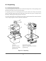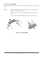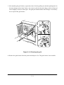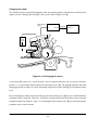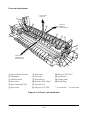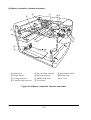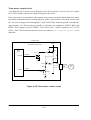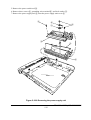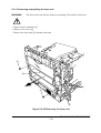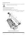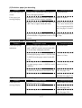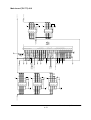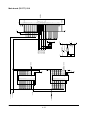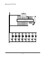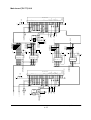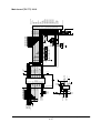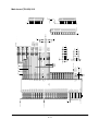
1
FS-1800/N FS-3800/N Page printers FS-1800/1800N/3800/3800N Series Combined Service Manual C Kyocera Corporation 2000 All rights reserved. Export Edition Notice The information in this manual is subject to change without notification. Additional pages may be inserted in future editions. The reader is asked to excuse any technical inaccuracies or typographical errors in the present edition. No responsibility is assumed if accidents occur while the service person is following the instructions in this manual. The contents of this manual are protected by copyright. No part of the manual may be reproduced or copied by any means without the permission of the copyright holder. Information This equipment has been tested and found to comply with the limits for a Class A*1/ Class B *2 digital device, pursuant to Part 15 of the FCC Rules. These limits are designed to provide reasonable protection against FS-1800/1800N | FS-3800/3800N harmful interference in a residential installation. This equipment generates, uses, and can radiate radio frequency energy and, if not installed and used in accordance with the instructions, may cause harmful interference to radio communications. However, there is no guarantee that interference will not occur in a particular installation. If this equipment does cause harmful interference to radio or television reception, which can be determined by turning the equipment off and on, the user is encouraged to try to correct the interference by one or more of the following measures. Reorient or relocate the receiving antenna. Increase the separation between the equipment and receiver. Connect the equipment into an outlet on a circuit different from that to which the receiver is connected. Consult the dealer or an experienced radio/TV technician for help. Changes or modifications not expressly approved by the manufacturer for compliance could void the user’s authority to operate the equipment. *1 : FS-1800N/FS-3800N *2 : FS-1800/FS-3800 Important notice to service person Before attempting service on the equipment, including disassembling, reassembling, troubleshooting, and adjustment, read this manual carefully. During performing service, use extreme care to avoid possible electric shock hazard, burn, and human injuries. Make sure the printer is not provided with any safety facilities other than those primarily intended for the safety of users. Regarding Tradenames PRESCRIBE is a registered trademark of Kyocera Corporation. PRESCRIBE 2e, KPDL, and KIR (Kyocera Image Refinement) are trademarks of Kyocera Corporation. Diablo 630 is a product of Xerox Corporation. IBM Proprinter X24E is a product of International Business Machines Corporation. Epson LQ-850 is a product of Seiko Epson Corporation. Hewlett-Packard, PCL, and PJL are registered trademarks of Hewlett-Packard Company. Centronics is a trade name of Centronics Data Computer Inc. PostScript is a registered trademark of Adobe Systems Incorporated. Macintosh is a registered trademark of Apple computer, Inc. Microsoft, Windows, and Windows NT are registered trademarks of Microsoft Corporation. PowerPC and Micro-Drive are trademarks of International Business Machines Corporation. CompactFlash is a trademark of SanDisk Corporation. ENERGY STAR is a U.S. registered mark. All other brand and product names are registered trademarks or trademarks of their respective companies. This Kyocera page printer uses PeerlessPrintXL to provide the HP LaserJet compatible PCL6 language emulation. PeerlessPrintXL is a trademark of The Peerless Group, Redondo Beach, CA 90278, U.S.A. This product was developed using the Tornado™ Real Time Operating System and Tools from Wind River Systems. Contains UFST ™ and MicroType ® from Agfa Corporation. Fine 1200 mode uses iRET image enhancement technology. iRET is a trademark of Oak Technology, Inc. FS-1800/1800N | FS-3800/3800N Conventions Throughout this manual, the following conventions are used: Italic letters refer related chapters or sections or documentations. This symbol followed by WARNING denotes that the following paragraph(s) includes precautions which, if ignored, could result in personal injury, and/or irrevocable damage to the printer. When followed by CAUTION this symbol denotes that the following paragraph(s) include the precautions which, if ignored, could result in damage to the printer. FS-1800/1800N | FS-3800/3800N About the chapters Unless otherwise specified, the content of this manual apply to both printer models of Ecosys FS1800, FS-1800N, FS-3800 and FS-3800N. The manual is comprised of the following chapters: Chapter 1: Product Information Chapter 2: Installation/Operation Chapter 3: Maintenance/Adjustments Chapter 4: Operation Overview Chapter 5: Disassembly Chapter 6: Troubleshooting Contents Appendix A: Diagrams Appendix B: Status Page Appendix C: Interface Contents Contents FS-1800/1800N | FS-3800/3800N REVISION HISTORY Version 1.00A 1.10 1.20 Date 23-Oct-2000 4-Dec-2000 4-Jul-2001 Replaced Pages 1-7, 3-12, 3-14, 3-15, 3-16, 4-37, 5-12, 5-37, 6-11,6-15, 6-16, 6-17, 6-18, 6-19, 6-20, 6-21, 6-22,6-23, 6-24, B-4, B-5 1-6, 1-7, 2-18, 2-20, 3-14, 3-15, 3-16, 3-19, 3-20 Remarks TO OBTAIN THE LATEST PRINTER DRIVERS AND UTILITIES, VISIT US AT OUR INTERNET HOME PAGE: http://www.kyocera.com/w2k FS-1800/1800N | FS-3800/3800N Chapter 1 Product Information Chapter 1 Contents 1-1 Printer specifications ...................................................................................................................... 1-3 1-1-1 Specifications ............................................................................................................................ 1-3 (1) Engine ....................................................................................................................................... 1-3 (2) Controller ................................................................................................................................... 1-4 (3) Weight and dimensions ............................................................................................................. 1-4 (4) Power requirements .................................................................................................................. 1-5 (5) Environmental requirements ...................................................................................................... 1-5 1-1-2 Available option memory/device ................................................................................................ 1-6 (1) Expansion memory (DIMM) ....................................................................................................... 1-6 (2) Memory card (CompactFlash) ................................................................................................... 1-7 (3) Hard disk (Microdrive) ............................................................................................................... 1-8 1-2 Names of parts ................................................................................................................................. 1-9 1-2-1 Names of parts .......................................................................................................................... 1-9 1-3 Safety information ......................................................................................................................... 1-10 1-3-1 Safety information .................................................................................................................... 1-10 (1) Laser safety ............................................................................................................................. 1-10 (2) Laser notice ............................................................................................................................. 1-10 (3) Laser caution label on the scanner unit ................................................................................... 1-10 (4) CDRH regulations (U.S.A.) ...................................................................................................... 1-12 (5) Ozone concentration ............................................................................................................... 1-12 (6) FCC statement (U.S.A.) ........................................................................................................... 1-12 a) For the FS-1800 and FS-3800 models ..................................................................................... 1-12 b) For the FS-1800N and FS-3800N models ................................................................................ 1-13 (7) Canadian Department of Communications compliance statement .......................................... 1-13 (8) Avis de conformité aux normes du ministère des Communications du Canada ..................... 1-13 (9) ISO 7779 ................................................................................................................................. 1-13 (10) CE marking directive ............................................................................................................. 1-14 (11) Declaration of conformity (Australia) ..................................................................................... 1-14 1-4 Environmental requirements ........................................................................................................ 1-15 1-4-1 Environmental conditions ........................................................................................................ 1-15 (1) Clearance ................................................................................................................................ 1-16 (2) Places to avoid ........................................................................................................................ 1-17 (3) Note on power ......................................................................................................................... 1-17 (4) Removing the printer ............................................................................................................... 1-18 1-5 About the toner container ............................................................................................................. 1-19 1-5-1 Toner container ....................................................................................................................... 1-19 (1) Toner container handling ......................................................................................................... 1-19 (2) Toner container storage .......................................................................................................... 1-20 1-1 Printer specifications 1-1-1 Specifications (1) Engine Item Print method Print speed (when printing multiple page) Resolution FS-1800/1800N Electrophotography laser scan 16 pages/min. (A4) 17 pages/min. (Letter) Fine 1200 mode Fast 1200 mode with KIR 600 dpi with KIR 300 dpi with KIR Smoothing KIR (Kyocera Image Refinement) First print (A4 or letter, 23 °C), Approximately 17.5 seconds or depends on input data less Warm-up time Standby: 20 seconds or less (23 °C ) Sleeping: 6.5 seconds or less Maximum duty cycle (A4) 65,000 pages/month Machine life expectancy 300,000 pages of printing or 5 years (expandable to 900,000 pages of printing using MK kits) Development Mono component dry developer Laser Visible laser Main charger Scorotron plus charging Transferring Negative charger roller Separation Curvature separation Drum cleaning Blade Drum discharging Eraser lamp (LED array) Fuser Heat roller and press roller Paper Plain paper Capacity of paper feed source Cassette: 500 sheets, (80 g/m2 [0.11 mm thickness]) MP tray: 100 sheets Capacity of output trays Face-up: 250 sheets, 2 (80 g/m [0.11 mm thickness]) Face-down: 250 sheets FS-3800/3800N ← 24 pages/min. (A4) 25 pages/min. (Letter) ← ← Approximately 9 seconds or less 35 seconds or less 35 seconds or less 100,000 pages/month ← ← ← ← ← ← ← ← ← ← ← ← FS-1800/1800N | FS-3800/3800N 1-3 (2) Controller Item CPU System ROM Font ROM Main (Video) RAM Maximum: Slot: DIMM size: Memory card (Optional) Hard disk (Optional) Host interface Parallel: Serial: Network interface card: (KUIO-LV [3.3 V]) Page description language Standard emulation modes FS-1800/1800N PowerPC405GF/200MHz 4 MB Mask (or Flash) DIMM 2 MB FS-1800 model: 8 MB FS-1800N model: 24 MB 264 MB (Including main RAM) 2 DIMM slots (A 16 MB DIMM is factoryinstalled in one slot for FS-1800N.) 16, 32, 64, 128 MB CompactFlash Microdrive (340 MB) High-speed, bidirectional (IEEE1284) RS-232C, Maximum speed: 115.2 Kbps 10/100 Base-TX, type IB-21 (Standard with equipped FS1800N) Prescribe PCL6, Diablo 630, IBM proprinter X24E, Epson LQ850, Line printer, KPDL FS-3800/3800N PowerPC740/200MHz ← ← FS-3800 model: 16 MB FS-3800N model: 32 MB 272 MB (Including main RAM) 2 DIMM slots (A 16 MB DIMM is factoryinstalled in one slot for FS-3800N.) ← ← ← ← ← 10/100 Base-TX, type IB-21 (Standard with equipped FS3800N) ← ← (3) Weight and dimensions Item Main unit (excluding protrusions) Width: Height: Depth: Weight: FS-1800/1800N 34.5 cm (13-9/16 inches) 30.0 cm (11-13/16 inches) 39.0 cm (15-3/8 inches) 13 Kg (28-5/8 lb.) FS-1800/1800N | FS-3800/3800N 1-4 FS-3800/3800N ← ← ← ← (4) Power requirements Item Voltage/current Watts FS-1800/1800N US/Canada: 120 V AC ±10 %, 60 Hz ±2 %/7.2 A Europe/Asia: 220 - 240 V AC ±10 %, 50/60 Hz ±2 %/3.6 A Average: FS-1800 model: 328 W FS-1800N model: 961 W Maximum: 120 V AC model: 961 W 220 - 240 V AC model: 961 W Standby (Ready): FS-1800 model: 21 W FS-1800N model: 23 W Sleeping: FS-1800 model: 14 W FS-1800N model: 15 W FS-3800/3800N ← ← FS-3800 model: 499 W FS-3800N model: 972 W 120 V AC model: 972 W 220 - 240 V AC model: 972 W FS-3800 model: 126 W FS-3800N model: 126 W FS-3800 model: 14 W FS-3800N model: 16 W (5) Environmental requirements Item Operating temperature and humidity Maximum altitude Noise emission (Excluding peaks, measured at 1 m from printer, as per ISO7779) FS-1800/1800N 10 to 32.5 °C (50 to 90.5 °F), 20 to 80 %RH 2,000 m (6,500 feet) Maximum: 53 dB(A) , Standby: 35 dB(A) FS-3800/3800N ← ← Maximum: 57 dB(A) , Standby: 39 dB(A) FS-1800/1800N | FS-3800/3800N 1-5 1-1-2 Available option memory/device (1) Expansion memory (DIMM) The following memory DIMMs are available for use with the printer. For more information about DIMM, refer to Section 2-2-4 Expanding the memory (DIMM) on page 2-11. NOTE Availability of the memory DIMMs, manufacturers, and specifications may change without notice. No responsibility is assumed by Kyocera Mita with respect to loss or damage caused by the use of these DIMMs. Manufacturer Melco Inc. Capacity 16 MB 32 MB 64 MB Model PM-HP-16M-KC PM-HP-32M-KC PM-HP-64M-KC 128 MB PM-HP-128M-KC FS-1800/1800N | FS-3800/3800N 1-6 This page is intentionally blank. FS-1800/1800N | FS-3800/3800N 1-7 (2) Memory card (CompactFlash) The following memory cards are available for use with the printer. Do not insert or remove a memory card (CompactFlash) while power is on. If the memory card is removed while the printer is on, damage could result in the printer’s electronics or the memory card. Refer to Section Installing the option memory card (CompactFlash) on page 2-16. NOTE Availability of the following memory cards (CompactFlash), manufacturers, and specifications may change without notice. No responsibility is assumed by kyocera Mita with respect to loss or damage caused by the use of these memory card. Manufacturer SanDisk Viking Kingston Capacity 8 MB 16 MB 24 MB 32 MB 48 MB 64 MB 96 MB 4 MB 8 MB 12 MB 16 MB 24 MB 32 MB 48 MB 64 MB 80 MB 8 MB 16 MB 24 MB 32 MB 48 MB 64 MB 96 MB FS-1800/1800N | FS-3800/3800N 1-8 Model SDCFBS-8-101 SDCFBS-16-101 SDCFBS-24-101 SDCFBS-32-101 SDCFBS-48-101 SDCFBS-64-101 SDCFBS-96-101 CF4M CF8M CF12M CF16M CF24M CF32M CF48M CF64M CF80M CF/8 CF/16 CF/24 CF/32 CF/48 CF/64 CF/96 Manufacturer DelkinDevices Inc. HITACHI Transcend SST LEXAR Media Capacity 8 MB 16 MB 24 MB 32 MB 48 MB 64 MB 96 MB 8 MB 16 MB 32 MB 48 MB 64 MB 4 MB 8 MB 16 MB 32 MB 8 MB 16 MB 24 MB 32 MB 48 MB 64 MB 96 MB 16 MB 32 MB 48 MB 64 MB 80 MB Model DDCFFLS2-008 DDCFFLS2-016 DDCFFLS2-024 DDCFFLS2-032 DDCFFLS2-048 DDCFFLS2-064 DDCFFLS2-096 HB286008C4 HB286016C4 HB289032C4 HB289048C4 HB288064C5 TS4MFLASHCP TS8MFLASHCP TS16MFLASHCP TS32MFLASHCP SST48CF008 SST48CF016 SST48CF024 SST48CF032 SST48CF048 SST48CF064 SST48CF096 - (3) Hard disk (Microdrive) The following hard disk is available for the printer: IBM Microdrive 340 MB capacity type FS-1800/1800N | FS-3800/3800N 1-9 1-2 Names of parts 1-2-1 Names of parts 1 0 2 ! 3 9 4 7 5 8 @ 6 # & ¤⁄ * ) ‹ ( 1 Top cover 2 Toner container 3 Operator panel 4 Paper gauge 5 Paper cassette 6 Paper size window 7 Power switch 8 Paper size dial 9 Waste toner bottle 0 Side cover $ ! Charger Cleaning knob % @ Paper stopper ^ # Face-down output tray $ Memory card slot ) Parallel interface connector % Paper feed unit ⁄ Serial interface connector ^ Paper feed unit release lever ¤ Option unit connector & MP tray ‹ Network interface card *1 *1 * Rear cover : Standard-installed with the FS-1800N/3800N ( AC inlet models (Normally covered with a cover plate) Figure 1-2-1 Name of parts FS-1800/1800N | FS-3800/3800N 1-10 1-3 Safety information 1-3-1 Safety information (1) Laser safety This printer is certified as a Class 1 laser product under the U.S. Department of Health and Human Services (DHHS) Radiation Performance Standard according to Radiation Control for Health and Safety Act of 1968. This means that the printer does not produce hazardous laser radiation. Since radiation emitted inside the printer is completely confined within protective housings and external covers, the laser beam cannot escape from the printer during any phase of user operation. (2) Laser notice This printer is certified in the U.S. to conform to the requirements of DHHS 21 CFR Subchapter for Class I (1) laser products, and elsewhere is certified as a Class I laser product conforming to the requirements of IEC 825. (3) Laser caution label on the scanner unit The laser scanner unit inside the printer has the following label affixed on its top. Observe the laser radiation warning and figures when handling the laser scanner unit. FS-1800/1800N | FS-3800/3800N 1-11 WARNING Use of controls or adjustments or performance of procedures other than those specified herein may result in hazardous radiation exposure. Laser radiation warning This label is affixed atop of the laser scanner unit inside the printer. FS-3800 US/Canada model FS-3800 Asian countries model Figure 1-3-1 Caution labels FS-1800/1800N | FS-3800/3800N 1-12 FS-3800 Europe/Pacific model (4) CDRH regulations (U.S.A.) The Center of Devices and Radiological Health (CDRH) of the U.S. Food and Drug Administration implemented regulations for laser products on August 2, 1976. These regulations apply to laser products manufactured after August 1, 1976. Compliance is mandatory for products marketed in the United States. A label indicating compliance with the CDRH regulations must be attached to laser products marketed in the United States. (5) Ozone concentration The printers generate ozone gas (O3) which may concentrate in the place of installation and cause an unpleasant smell. To minimize concentration of ozone gas to less than 0.1 ppm, we recommend you not to install the printer in a confined area where ventilation is blocked. (6) FCC statement (U.S.A.) a) For the FS-1800 and FS-3800 models This device complies with Part 15 of the FCC Rules. Operation is subject to the following two conditions: (1) This device may not cause harmful interference, and (2) this device must accept any interference received, including interference that may cause undesired operation. This equipment has been tested and found to comply with the limits for Class B digital device, pursuant to Part 15 of the FCC Rules. These limits are designed to provide reasonable protection against harmful interference in a residential installation. This equipment generates, uses, and can radiate radio frequency energy and, if not installed and used in accordance with the instructions, may cause harmful interference to radio communications. However, there is no guarantee that interference will not occur in a particular installation. If this equipment does cause harmful interferences to radio or television reception, which can be determined by turning the equipment off and on, the user is encouraged to try to correct the interference by one or more of the following measures: • Reorient or relocate the receiving antenna. • Increase the separation between the equipment and receiver. • Connect the equipment into an outlet on a circuit different from that to which the receiver is connected. • Consult the dealer or an experienced radio/TV technician for help. Changes or modifications not expressly approved by the manufacturer for compliance could void the user’s authority to operate the equipment. Shielded circular cable should be used for interfacing with the computer. FS-1800/1800N | FS-3800/3800N 1-13 Any modification without prior permission may cause harmful interference. If any modification/change is introduced to this equipment without prior permission, Kyocera as the manufacturer cannot guarantee compliance with FCC rules. To use equipment which does not comply with FCC rules is prohibited. The printer may be optionally installed with the following units: Options conforming to the Class B limit • Sorter SO-60 • Duplexer DU-60 • Paper feeder PF-60 b) For the FS-1800N and FS-3800N models This equipment has been tested and found to comply with the limits for Class A digital device, pursuant to Part 15 of the FCC Rules. These limits are designed to provide reasonable protection against harmful interference when the equipment is operated in a commercial environment. This equipment generates, uses, and can radiate radio frequency energy and, if not installed and used in accordance with the instruction manual, may cause harmful interference to radio communications. Operation of this equipment in a residential area is likely to cause harmful interference in which case the user will be required to correct the interference at his own expense. WARNING FCC Regulations state that any unauthorized changes or modifications to this equipment not expressly approved by the manufacturer could void the user’s authority to operate the equipment. (7) Canadian Department of Communications compliance statement This Class B digital apparatus complies with Canadian ICES-003. (8) Avis de conformité aux normes du ministère des Communications du Canada Cet appareil numérique de la classe B est conforme à la norme NMB-003 du Canada. (9) ISO 7779 Maschinenlärminformationsverordnung 3. GSGV, 18.01.1991: Der höchste Schalldruckpegel beträgt 70 dB(A) oder weniger gemäß ISO 7779. FS-1800/1800N | FS-3800/3800N 1-14 (10) CE marking directive According to Council Directive 89/336/EEC and 73/23/EEC declares that the product Product name: Page printer Model name: FS-1800/FS-3800/FS-1800N/FS-3800N (as tested with the enhancement optional unit: PF-60, DU-60 and SO-60) Conforms to the following product specifications. EN 55 022:1998 Class B EN 61 000-3-2:1995 EN 61 000-3-3:1995 EN 55 024:1998 EN 60 950:1992 (+A1+A2+A3+A4+A11) EN 60 825-1:1994+A11 (11) Declaration of conformity (Australia) declares that the product Product number: Page printer Model name: FS-1800/FS-3800/FS-1800N/FS-3800N (as tested with the enhancement optional units: PF-60, DU-60 and SO-60) Description of device: This page printer model FS-3800 is the 24 ppm (FS-1800 is the 16 ppm); A4 size and utilizes plain paper; laser; dry toner, etc. The printer can be equipped with several enhancement optional units such as a paper feeder PF-60, a duplexer DU-60, a sorter SO-60, etc. Ther printer conforms to the following product specifications: AS/NZS 3548; 1995 (EN 55 022:1994 Class B) IEC60950 (EN 60 950:1992+A1+A2+A3+A4+A11) IEC60825-1 (EN 60 825-1:1994+A11) FS-1800/1800N | FS-3800/3800N 1-15 1-4 Environmental requirements 1-4-1 Environmental conditions The Environmental requirements section on page 1-5 should be observed to ensure the optimum operation of the printer. The use of the printer in a location which does not satisfy the requirements may result in troubles and risk shortening its service life. The printer will work best if it is installed in a location that is: • Level and well supported (Place the printer on a table or desk.) • Not exposed to sunlight or other bright light (not next to an uncurtained window). Do not place the printer on an unstable cart, stand or table. • Near an AC wall outlet, preferably one that can be used for the printer alone. The outlet should have a ground slot, or an adapter should be used. If you use an extension cord, the total length of the power cord plus extension cord should be 17 feet or 5 meters or less. • Well ventilated, not too hot or cold, and not too damp or dry (See section Environmental requirements on page 1-5). If you install the printer where the temperature or humidity is outside the requirements in section Environmental requirements in chapter 1, the best print quality may not be expected and there will be an increased chance of paper jams. • Provide a sufficient clearances around the printer to ensure ventilation and ease of access. (See section Clearance on next page). FS-1800/1800N | FS-3800/3800N 1-16 (1) Clearance Allow the necessary minimum clearance on all sides of the printer as below. 5 4 1 3 2 Figure 1-4-1 Clearances Ref. 1 2 3 4 5 Clearance Left Front Right Back Head room Dimensions [Minimum] 30 cm (11-13/16 inches) 60 cm (23-5/8 inches) 25 cm (9-7/8 inches) 20 cm (7-7/8 inches) 30 cm (11-13/16 inches) FS-1800/1800N | FS-3800/3800N 1-17 (2) Places to avoid Avoid installing the printer in locations exposed to: • Direct drafts of hot or cold air. • Direct drafts of outside air. (Avoid locations next to outside doors.) • Sudden temperature or humidity changes. • Any source of high heat, such as a radiator or stove. • Excessive dust. Dust and smoke may cause contamination on the laser scanner window, causing print quality problem. • Vibration. • Ammonia fumes or other harmful fumes. (In case of fumigating the room or saturate it with insecticide, remove the printer first.) • Avoid greenhouse-like rooms. (Because of sunlight and humidity.) • Avoid enclosed spaces that block ventilation. • Avoid sites more than 6,500 feet or 2,000 meters above sea level. (3) Note on power Use only the power source voltage conforming to the printer’s rated power voltage. Do not use other power sources. • Disconnect the printer from the power source before attempting removal or replacement of an electrical component or a printed-circuit board. • The printer should not be connected to a power source until the instruction is given to do so when performing tests described in this manual. • In connecting the printer power, exercise an extreme care in handling the power supply or any other electric parts which may give an electric shock. • Before performing maintenance or repair, power from both the power source and the associated peripheral devices (computer, sorter, etc.) should be disconnected, unless otherwise specified. • To avoid possible electrical shock, extreme caution must be exercised in handling the power cord and any other electrical part. • An easily accessible socket outlet must be provided near the equipment. WARNING As the disconnect device is not incorporated in the printer’s AC primary circuit, an easily accessible socket outlet must be provided near the equipment. FS-1800/1800N | FS-3800/3800N 1-18 (4) Removing the printer Observe the following precautions in removal and transportation of the printer. • Be sure to repack the printer in its original carton. • Do not leave the printer, toner container, process unit and other printer modules inside a vehicle if the outdoor temperature is more than 25 °C. As unexpectedly high temperature may develop inside when a vehicle is parked for a long period of time, the drum, toner container, process unit and the supplies should be removed from the vehicle. The vehicle during transportation should be parked in the shade or with the window open to allow minimum air circulation or the adequate air conditioning should be made. • Should the printer be left in a vehicle, it may not be exposed to the temperature change of more than 7 °C within 30 minutes. • Before removing the printer to a warm place, wrap it in a blanket, etc., before crating it. Allow approximately two to three hours after having moved after uncrated. Failure to observe the above may result in moisture condensation which will affect the performance of the printer. FS-1800/1800N | FS-3800/3800N 1-19 1-5 About the toner container 1-5-1 Toner container The printer should use a Kyocera TK-60/TK-60E toner kit. To ensure the high print quality and long service life, the following handling precautions should apply: CAUTION As the Ecosys printers are designed to ensure the optimum print quality when used with Kyocera’s proprietary toner, Kyocera do not recommend to use any refilled toner containers that may be available commercially. This is because Kyocera have no means of control over how such refilled toner could affect the print quality and the reliability of the printer. (1) Toner container handling To loosen and mix the toner inside before use, with the label side down, thoroughly shake the toner container 1 (in the direction of the arrows) ten times or more. 1 Figure 1-5-1 Toner container handling CAUTION The toner container is not designed for disassembly or refilling. Do not attempt to disassemble or refill the toner container. FS-1800/1800N | FS-3800/3800N 1-20 (2) Toner container storage The toner contained in the container is susceptible to temperature and humidity. To ensure the high print quality, store the toner container in a place that satisfies the following environmental conditions: Temperature: Humidity: −20 to 40 °C (−4 to 104 °F) 15 to 90 % RH NOTE If the toner container is removed from the printer’s developer, put it in a protective bag and keep it in a dark place. CAUTION If the printer is shipped for return, etc., do not ship it with the toner container installed. Remove the toner container from the developer and put in a plastic bag and seal the plastic bag. Otherwise, toner may leak and contamination may result in the printer. FS-1800/1800N | FS-3800/3800N 1-21 Chapter 2 Installation/Operation Chapter 2 Contents 2-1 Unpacking ......................................................................................................................................... 2-3 2-1-1 Unpacking and inspection ......................................................................................................... 2-3 2-2 Installing the printer ........................................................................................................................ 2-5 2-2-1 Installing the toner container ..................................................................................................... 2-5 Removing the toner container ......................................................................................................... 2-7 2-2-2 Installing the waste toner bottle ................................................................................................. 2-8 Removing the waste toner bottle .................................................................................................... 2-9 2-2-3 Developer initialization (automatic) .......................................................................................... 2-10 2-2-4 Expanding the memory (DIMM) ............................................................................................... 2-11 (1) Minimum memory requirements .............................................................................................. 2-11 (2) DIMM specifications ................................................................................................................ 2-11 (3) Notes on handling DIMM ......................................................................................................... 2-12 (4) Installing the DIMM .................................................................................................................. 2-13 (5) Testing the expansion memory ............................................................................................... 2-14 (6) Installing the option hard disk (Microdrive) .............................................................................. 2-15 (7) Installing the option memory card (CompactFlash) ................................................................. 2-16 (8) Installing the option network interface card ............................................................................. 2-17 2-3 Using the operator panel ............................................................................................................... 2-18 2-3-1 Operator panel ......................................................................................................................... 2-18 (1) Indicators and keys .................................................................................................................. 2-18 (2) Interface indicator .................................................................................................................... 2-20 (3) Paper size indicator ................................................................................................................. 2-20 (4) Paper type Indicator ................................................................................................................ 2-21 (5) Message display ...................................................................................................................... 2-22 2-3-2 Menu selection system ............................................................................................................ 2-23 (1) Menu selection and sequence ................................................................................................. 2-23 2-1 Unpacking 2-1-1 Unpacking and inspection The printer package should contain the items as shown in the figure below. After unpacking, remove the printer and all the accessories from the package. For unpacking, place the box containing the printer on a flat, stable surface. Remove the manuals, toner kit, and other items located on top of the spacer. Then remove the spacer. Carefully remove the printer. Obtain help from other persons if necessary. For the FS-1800N/3800N, the CD-ROM (Network library) and the manual for the network interface card are shipped together with the components listed below. 7 56 1 2 4 3 1 Printer 2 Toner container 3 Waste toner bottle 4 Power cord 5 Installation manual 6 Kyocera digital library CD-ROM 7 Plastic bag Figure 2-1-1 Unpacking FS-1800/1800N | FS-3800/3800N 2-3 1 2 3 6 5 1 Printer 2 Toner container 3 Waste toner bottle 4 Power cord 7 5 Installation manual 6 Kyocera digital library CD-ROM 7 Plastic bag Figure 2-1-2 List of shipped components FS-1800/1800N | FS-3800/3800N 2-4 4 2-2 Installing the printer Installing the printer requires several steps. Proceed as follows in sequence. 2-2-1 Installing the toner container 1. Open the top cover all the way. 2. Take toner container 1 from the bag. With the label side down and pivoting on the middle of the container, thoroughly shake the toner container (in the direction of the arrows) ten times or more to loosen and mix the toner inside. 1 Figure 2-2-1 Shake the toner container FS-1800/1800N | FS-3800/3800N 2-5 3. Carefully remove the protective seal 2. 2 Figure 2-2-2 Removing the protective seal 4. Install the toner container 2 into the printer. 5. Push firmly on the top of the toner container 2 at the positions marked [PUSH HERE]. Figure 2-2-3 Installing the toner container FS-1800/1800N | FS-3800/3800N 2-6 Removing the toner container To remove the toner container, pull the lock lever (green colored) 1 and gently lift the toner container. NOTE Do not remove the toner container unless you need to do so for servicing, etc. 1 Figure- 2-2-4 Removing the toner container FS-1800/1800N | FS-3800/3800N 2-7 2-2-2 Installing the waste toner bottle The waste toner bottle must be installed in the printer. It must be properly fitted inside the left side cover as explained below. 1. Open the cap 1 of the waste toner bottle 2. 2. Open the side cover 3 and install the waste toner bottle 2 so that it is properly seated in the area under the drum unit. 3. Close the side cover 3. 2 2 1 3 3 Figure 2-2-5 Installing the waste toner bottle FS-1800/1800N | FS-3800/3800N 2-8 Removing the waste toner bottle To remove the waste toner bottle 1, while holding the waste toner bottle 1, press the lock lever 2 aside, then gently remove the waste toner bottle 1 sideways. NOTE Do not remove the waste toner bottle unless you need to do so for service, etc. 2 1 Figure 2-2-6 Removing the waste toner bottle FS-1800/1800N | FS-3800/3800N 2-9 2-2-3 Developer initialization (automatic) The printer is shipped from the factory with no toner installed in the developer. In order for the printer to be operable, the developer must be filled with a sufficient amount of toner necessary to continuously support print jobs. This is called developer initialization and automatically executed when the printer is turned on for the first time. Developer initialization takes up to 15 minutes for the original developers (DV-60 for the FS-1800 and DV-61 for the FS-3800) or 8 minutes for the service developer (DV-62 for both models). NOTE Do not turn printer power off during the developer is initialized. If the printer is switched off in the middle of developer initialization, even after the printer is switch on again, the printer will not automatically resumes developer initialization. Should this be the case, enforce the printer to resume developer initialization in the following manner: 1. While the printer is turned off, press and hold the GO and CANCEL keys. 2. Turn printer power on. 3. Let go off of the GO and CANCEL keys for more than 5 seconds. Developer initialization resumes for the rest of the required total time. 4. Wait until the READY indicator is lit and the message display indicates Ready. 5. Make a test print by printing a status page. To print a test page, proceed as follows; 1 Press the MENU key on the printer. 2 Press the key or key repeatedly until the message display shows Print Status Page. 3 Press the ENTER key twice. 6. If the status page is printed satisfactorily, setup is complete. If not, investigate whether all step procedures are properly followed. FS-1800/1800N | FS-3800/3800N 2-10 2-2-4 Expanding the memory (DIMM) The FS-1800/1800N comes standard-equipped with 8 MB of main memory; the FS-3800/3800N comes with 16 MB of memory. The FS-1800/1800N can be expanded up to the maximum of 264 MB (8 MB + 256 MB), and the FS-3800/3800N can be expanded up to the maximum of 272 MB (16 MB + 256 MB). For all models, expansion should be done using optional DIMMs (Dual Inline Memory Module). (1) Minimum memory requirements Printing environment PCL6, duplex mode = None PCL6, duplex mode = On KPDL, duplex mode = None KPDL, duplex mode = On PCL6/KPDL resource protection, duplex mode = None PCL6/KPDL resource protection, duplex mode = ON 300 dpi 8 MB 8 MB 8 MB 8 MB - Resolution 600 dpi 1200 dpi Fast mode Fine mode 8 MB 8 MB 8 MB 8 MB 8 MB 12 MB 8 MB 8 MB 8 MB 8 MB 12 MB 12 MB 10 MB 10 MB 10 MB 14 MB 14 MB 14 MB (2) DIMM specifications Item Memory size in MB Number of pins Access speed Parity Bus width Specification 16, 32, 64, 128 MB 100 pins 66 MHz None 32 bits FS-1800/1800N | FS-3800/3800N 2-11 (3) Notes on handling DIMM Before proceeding to install DIMM, to protect the main board and DIMMs, read the following notes: NOTE • Before touching a DIMM, touch a water pipe or other large metal object to discharge yourself of static electricity. • While doing the work, it is recommended that you wear an antistatic wrist strap. • Touch the main board and DIMM only by the edges, not in the middle. Figure 2-2-7 Handling DIMM FS-1800/1800N | FS-3800/3800N 2-12 (4) Installing the DIMM The main board of the printer is equipped with two sockets for installing extra DIMMs. NOTE A 16 MB DIMM is already installed in one socket for FS-1800N/3800N models. CAUTION Be sure that no foreign objects such as metal chips or liquid get inside the printer during installing DIMMs. Operation of the printer during the presence of a foreign substance may lead to fire or electric shock. WARNING Before proceeding installation, turn the printer’s power switch off. Unplug the printer’s power cable and disconnect the printer from the computer or the network. 1. Turn the power switch off. 2. Remove the memory card (CompactFlash) that may be inserted in the memory card slot 1 at the left side of the printer. 3. Remove the main board 2 by removing the two (plated) screws 3. 4. Pull the main board 2 all the way out of the printer. 2 1 3 3 Figure 2-2-8 Removing the main board FS-1800/1800N | FS-3800/3800N 2-13 5. Open the clips 4 on both ends of the DIMM socket 5. 6. Insert the DIMM 6 into the DIMM socket 5 so that the notches on the DIMM align with the corresponding protrusions in the slot. 6 4 4 5 Figure 2-2-9 Inserting the DIMM (1) 7. Close the clips 4 on the DIMM socket 5 to secure the DIMM 6. 6 4 5 4 Figure 2-2-10 Inserting the DIMM (2) (5) Testing the expansion memory To test the expansion memory, turn printer power on and print a status page. If the installation has been successful, the Available Memory item of the status page will show the expanded memory size corresponding to the amount of memory added. FS-1800/1800N | FS-3800/3800N 2-14 (6) Installing the option hard disk (Microdrive) The main board of the printer is equipped with a socket for the hard disk (Microdrive). If the hard disk is installed in the printer, received data can be rasterized and stored on this hard disk. This enables high-speed printing of multiple copies using an electronic sort function. Also, by using the quick copy job function or private/stored job function, desired documents can be printed at any later time. For details of these functions, refer to the printer’s Users Manual. CAUTION Take precautions that no foreign objects such as metal chips or liquid get inside the printer during the installation process. Operation of the printer during the presence of a foreign objects may lead to fire or electric shock. WARNING Turn the printer’s power switch off. Unplug the printer’s power cable and disconnect the printer from the computer or the network. 1. Turn the power switch off. 2. Remove the main board 1 from the printer. (See step 2 to 4, on page 2-13.) 3. Install the hard disk 2 to the hard disk slot 3. 3 2 1 Figure 2-2-11 Installing the option hard disk FS-1800/1800N | FS-3800/3800N 2-15 (7) Installing the option memory card (CompactFlash) CAUTION Do not insert or remove a memory card (CompactFlash) while power is on. If the memory card is removed while the printer is on, damage could result in the printer’s electronics or the memory card. 1. Turn the power switch off. 2. Insert the memory card 1 in the memory card slot 2 at the right bottom of the printer. Insert it face up, connector end first. Push it in all the way. 2 1 Figure 2-2-12 Installing the option memory card FS-1800/1800N | FS-3800/3800N 2-16 (8) Installing the option network interface card The main board of the printer is equipped with a network interface card slot (KUIO-LV type, 3.3 V). The FS-1800N and FS-3800N have a network interface card IB-21 already installed at the factory. CAUTION Be sure that no foreign object such as metal chips or liquid get inside the printer during the installation process. Operation of the printer during the presence of a foreign object may lead to fire or electric shock. WARNING Turn the printer’s power switch off. Unplug the printer’s power cable and disconnect the printer from the computer. 1. Turn the power switch off. 2. Remove the two screws 1 then remove the option interface card slot cover 2. 3. Insert the network interface card 3 to the option interface card slot 4. 4. Fix the network interface card 3 by two screws 1. 5. Connect the network cable 5 to the network interface card 3. 6. Set the network address from the printer operator panel. (Refer to the printer’s User’s Manual) 2 1 3 5 4 3 Figure 2-2-13 Installing the option network interface card FS-1800/1800N | FS-3800/3800N 2-17 2-3 Using the operator panel This section provides explanation on how to use the printer’s operator panel. For details on operating the printer, refer to the printer’s User’s Manual. 2-3-1 Operator panel The printer’s operator panel has the following indicators, keys and message display. Note that adjustments made using these keys may be overridden by those made from within the application software. 1 23 Message display $ # @ 4 9 7 0 5 6 8 ! Figure 2-3-1 Operator panel (1) Indicators and keys Indicator 1 READY indicator Condition Flashing Lit Off 2 DATA indicator Flashing Lit 3 ATTENTION indicator Flashing Lit Off Description An error has occurred that the user can clear. The printer is on-line and ready to print. The printer is off-line. The printers stores but does not print received data. This is also indicates when printing is automatically stopped due to the occurrence of an error. Data transfer between the printer and the computer is taking place. Either data is being processed, or data is being written onto the option CompactFlash or Microdrive. The printer needs maintenance attention or the printer is warming up (Please wait). A problem or an error has occurred that the user can clear, for example, paper jam. Operations are normal. FS-1800/1800N | FS-3800/3800N 2-18 Key 4 GO key 5 CANCEL key 6 MENU key 7 key 8 key 9 < key 0 > key ( key) ! ENTER key Function • Switches the printer on-line and off-line. • Prints and feed out one page. • Cancels a printing job. To cancel a print job, proceed as follows: 1. Check the message Processing is displayed in the message display. 2. Press the CANCEL key. 3. The message Print Cancel? will appear in the message display and the interface to be canceled will be displayed. Parallel Serial Option (appears only when an [option] network interface card is installed) Press the CANCEL key again if you wish to stop the cancellation of printing. 4. Selecting the interface to cancel using the or key. Then press the ENTER key. Printing from the interface selected will be stopped. The Cancelling data message appears in the message display and printing stops after the printer finishes printing the current page. • Resets numeric values, or cancels a setting procedure. • Stops the sound alarm that indicates the occurrence of an error. • Enter menu mode • When pressed during menu selection, terminates the setting and returns to the Ready condition. Lets you access the desired item or enter numeric values. In some of the control procedures, the < and > keys are used to enter or exit the sub items. Enables access to the desired item or entering of numeric values. In some of the control procedures, the < and > keys are used to enter or exit the sub items. Used as the < key in the menu selection. • Used as the > key in the menu selection. • Displays on-line help messages on the message display when paper jam occur. When pressed in the Ready condition, displays on-line help messages. Finalizes numeric values and other selections in menu selection. FS-1800/1800N | FS-3800/3800N 2-19 (2) Interface indicator The INTERFACE indicator $ shows which of the printer's interfaces is currently active. It uses the following abbreviations: Message --PAR SER OPT Meaning No interface is currently used Standard bidirectional parallel interface Serial interface (RS-232C) [Option] network interface card The PAR , SER , or OPT indicator flashes when the printer is receiving data and remains indicated for the duration of the interface time-out time. (3) Paper size indicator The SIZE indicator # indicates the size of the current paper cassette. Default is Letter size for the U.S.A. and A4 for European countrie. While the printer is Processing data to print, the SIZE indicator switches to indicate the paper size selected by the application software. The following abbreviations are used to indicate paper sizes. Message A4 DL A5 C5 A6 b5 B5 EX B6 #6 LT #9 LG HA MO OH BU CU Paper size ISO A4 (21 × 29.7 cm) ISO DL (11 × 22 cm) * ISO A5 (14.8 × 21 cm) ISO C5 (16.2 × 22.9 cm) * ISO A6 (10.5 × 14.8 cm) * ISO B5 (17.6 × 25 cm) * JIS B5 (18.2 × 25.6 cm) Executive (7-1/4 × 10-1/2 inches) * JIS B6 (12.8 × 18.2 cm) * Commercial 6-3/4 (3-5/8 × 6-1/2 inches) * Letter (8-1/2 × 11 inches) Commercial 9 (3-7/8 × 8-7/8 inches) * Legal (8-1/2 × 14 inches) Japanese postcard (10 × 14.8 cm) * Monarch (3-7/8 × 7-1/2 inches) * Return postcard (20 × 14.8 cm) * Business (4-1/8 inches) * Custom size (14.8 × 21 cm to 21.6 × 35.6 cm) * with only the MP tray feeding FS-1800/1800N | FS-3800/3800N 2-20 (4) Paper type Indicator The TYPE indicator @ indicates paper types. The following abbreviations are used to indicate paper types. Message Paper type (none) Auto ROUGH Rough PLAIN Plain LETTERHEA Letterhead TRNSPRNCY Transparency* COLOR Color PREPRINTE Preprinted PREPUNCH Prepunched LABELS Labels* ENVELOPE Envelope* BOND Bond CARDSTOCK Cardstock* RECYCLED Recycled CUSTOM1(to 8) Custom 1 (to 8) VELLUM Vellum* * with only the MP tray feeding FS-1800/1800N | FS-3800/3800N 2-21 (5) Message display The message display gives information in the form of short messages. The six messages listed below are displayed during normal warm-up and printing. Other messages appear when the printer needs the operator's attention as explained in Chapter 6 Troubleshooting. Message Self test Please wait Ready Processing Waiting Sleeping Cancelling data FormFeed Time Out Meaning The printer is self-testing after power-up. The printer is warming up and is not ready. When the printer is switched on the first time after the toner container is installed, (Adding toner) also appears. The printer is ready to print. The printer is receiving data, generating graphics, reading an memory card (CompactFlash)/hard disk (Microdrive), or printing. The printer is waiting for a command that says the job is over before printing the last page. Pressing the GO key allows you to obtain the last page immediately. The printer is in Sleep mode. The printer wakes from Sleep mode whenever a key on the operator panel is pressed, the cover is opened or closed, or data is received. The printer then warms up and goes on-line. (The time that it takes the printer to enter Sleep mode depends on the Sleep Timer setting.) Data inside the printer is being canceled. The printer prints the last page after a waiting period. FS-1800/1800N | FS-3800/3800N 2-22 2-3-2 Menu selection system The MENU key on the operator panel allows you to use the menu selection system to set or change the printer environment such as the paper source, emulation, etc. Settings can be made when Ready is indicated on the printer message display. The printer obeys the most recently received printer settings sent from the application software, or from the printer driver, which take priority over operator panel settings. (1) Menu selection and sequence The following is the hierarchy diagram of the menu selection system of the printer. Ready PAR A4 PLAIN These items will not show unless the printer is installed with the applicable option unit. Print Menu Map Print Status Page e-MPS Interface Serial > >Bau rate 9600 > >Data Bits 8 >Quick Copy >Stop Bits 1 >Private/Stored >Parity None >Print VMB Data >Protocol DTR (pos.)&XON >List of VMB >Barcode Mode Off Interface Option >List of Code JOB > >NetWare Off >e-MPS > Configuration >NetWare On >>Quick Copy >>NetWare Frame Auto >>Temp.Code JOB Size Inter face Parallel > >>Perm.Code JOB Size >TCP/IP Off >>VMB Size >TCP/IP On > >>DHCP Off > >>IP Address >Parallel I/F Nibble (high) >>Subnet Mask >Parallel I/F Auto >>Gateway >Parallel I/F Normal >Ether Talk Off >Parallel I/F High Speed >OPT. StatusPage Off Continued on next page. FS-1800/1800N | FS-3800/3800N 2-23 Emulation PCL 6 Font Option > >Code set ISO-6 ASCII Emulation KPDL > I000 >Courier Dark > >Print KPDL errs Off >Courier Regular >Print KPDL errs On Emulation KPDL (AUTO) > >Letter Gothic Regular > >Letter Gothic Dark >Alt. Emulation PCL 6 >Size 012.00 point(s) >Print KPDL errs Off >Pitch >Print KPDL errs On >List of Fonts 10.00 cpi Emulation > IBM Proprinter Page set >Code set IBM US > >Copies Emulation Line printer > 001 >Orientation Portrait >Code set IBM US Emulation DIABLO 630 >Orientation Landscape > >Page Protect Auto >Code set DIABLO US Emulation EPSON LQ-850 >Page Protect On > >Code set LQ US Font Internal >LF Action LF only >LF Action CR and LF > > I000 >LF Action Ignore LF >Courier Dark >CR Action LF only >Courier Regular >CR Action CR and LF >Letter Gothic Regular >CR Action Ignore CR >Letter Gothic Dark >Wide A4 Off >Size 012.00 point(s) >Wide A4 On >Pitch 10.00 cpi >List of Fonts Continued on next page. FS-1800/1800N | FS-3800/3800N 2-24 Print Quality > Memory Card > >KIR Mode On >Read Fonts >KIR Mode Off >Read Data >Ecoprint Mode Off >Write Data >Ecoprint Mode On >Delete Data >Resolution Fast 1200 mode >List of Partitions >Resolution Fine 1200 mode >Resolution 300 dpi >Resolution 600 dpi >Print Density 03 Opt. ROM > >Read Data >List of Partitions Hard Disk > >Read Data >Write Data >Delete Data >List of Partitions RAM Disk Mode On RAM Disk Mode Off >RAM Disk Size >Read Data >Write Data >Delete Data >List of Partitions Continued on next page. FS-1800/1800N | FS-3800/3800N 2-25 Paper Handling > >MP Tray Mode First >MP Tray Size A4 or Letter LIFE Counters >MP Tray Type Plain > >Total Print >EF Size DL or Business >New Toner Installed >EF Type Plain Others > >BulkFeeder Size >Form Feed Time Out 030sec. >BulkFeeder Type Plain >Sleep Timer > 005 min. >Cassette Size > >>Sleep Mode On >>Unit mm >>Sleep Mode Off >>Unit inch >Print HEX-DUMP >>X Dimension >Printer Reset >>Y Dimension >Cassette Type Plain >Resource prot. Off >Feed Select Cassette >Resource prot. Permanent >Duplex Mode None >Resource prot. Perm / Temp >Stack Select Face-down tray >Buzzer On >Opt.StackerMode Sorter >Buzzer Off >Override A4/LT Off >Auto Continue Mode On >Override A4/LT On >Type Adjust Custom 1 >>Auto Continue Timer 000sec. > >Auto Continue Mode Off >>Paper weight Normal >Service >>Paper weight Heavy (Thick) > >>Print Status Page >>Paper weight Light (Thin) >>Toner ID >>Duplex Path Disable >>Developer >>Duplex Path Enable >>Drum >Reset Type Adjust FS-1800/1800N | FS-3800/3800N 2-26 Chapter 3 Maintenance/Adjustments Chapter 3 Contents 3-1 Maintenance/Adjustments .............................................................................................................. 3-3 3-1-1 Life expectancy of modules ....................................................................................................... 3-3 3-1-2 Toner container ......................................................................................................................... 3-4 (1) When to replace the toner container ......................................................................................... 3-4 (2) Notes on changing the toner container ...................................................................................... 3-4 (3) Toner container replacement ..................................................................................................... 3-5 (4) Toner saver mode (EcoPrint) .................................................................................................... 3-6 (5) Replacing the waste toner bottle ............................................................................................... 3-7 3-1-3 Cleaning the printer ................................................................................................................... 3-8 (1) Main charger unit ....................................................................................................................... 3-8 (2) Cleaning the main charger wire and grid ................................................................................... 3-9 Main charger wire ........................................................................................................................... 3-9 Grid ............................................................................................................................................... 3-10 (3) Paper feed unit ........................................................................................................................ 3-12 (4) Replacing the developer .......................................................................................................... 3-13 Shipping the developer ................................................................................................................. 3-13 (5) Developer initialization (Toner install mode) ............................................................................ 3-14 (6) Developer refreshing mode ..................................................................................................... 3-15 (7) Drum cleaning mode ............................................................................................................... 3-16 3-1-4 Updating the firmware ............................................................................................................. 3-17 (1) Firmware program data format ................................................................................................ 3-18 (2) Downloading the engine and controller firmware .................................................................... 3-18 From the parallel interface ............................................................................................................ 3-18 From the memory card (CompactFlash) ....................................................................................... 3-20 (3) Downloading operator panel message data ............................................................................ 3-21 (4) Downloading errors ................................................................................................................. 3-22 3-1 Maintenance/Adjustments 3-1-1 Life expectancy of modules The table below shows the nominal life expectancy for modules. Detailed part information for each module (except toner containers) can be found in the separate Parts Catalog. Table 3-1-1 Life expectancy of modules Module Toner container*1 Drum unit Developer Fuser unit Main charger unit Refurbishment kit*2 Model FS-1800/1800N FS-3800/3800N TK-60 TK-60E DK-60 DK-61 DV-60 DV-61 DV-62 FK-60*3 FE-60 MK-60 Nominal life (pages) 20,000 10,000 300,000 300,000 300,000 FK-61*3 FE-61 MK-61 300,000 300,000 300,000 *1 : User-replaceable *2 : Includes DK, DV, and FK kits and a feed-transfer unit. *3 : Each FK kits have two voltage type for 120 V AC and 220 - 240 VAC. FS-1800/1800N | FS-3800/3800N 3-3 3-1-2 Toner container Assuming an average toner coverage of 5 % with EcoPrint mode turned off, the toner container TK-60 will need replacing approximately once every 20,000 pages; the toner container TK-60E, approximately once every 10,000 pages. Kit Life in pages TK-60 20,000 TK-60E 10,000 Based on letter or A4 size paper; average print coverage of 5 % NOTE Table 3-1-2 Toner container A new printer in which a toner kit TK-60 is installed for the first time, the number of copies that can be printed will be limited to approximately 10,000 pages. (1) When to replace the toner container When the printer runs low on toner, Toner low TK-60 display and ATTENTION indicator lit on the operation panel. Be sure to promptly replace the toner container and clean the inside of the printer when this message appears. If the printer stops printing while Replace toner TK-60 is display, replace the toner container to continue printing. (2) Notes on changing the toner container Observe the following cautions when replacing the toner container: • Do not attempt to disassemble the old toner. • Do not attempt to reuse the waste toner inside. • Keep magnetic media such as floppy disks away from the toner container. • Be sure to clean the parts as instructed in section 3-1-1 Cleaning the printer on page 3-8 at the same timing of replacing toner container. • Use of the Kyocera toner kit TK-60/TK-60E is highly recommended for the optimum operation of the printer. FS-1800/1800N | FS-3800/3800N 3-4 (3) Toner container replacement To replace the toner container, open the top cover. Pull the lock lever 1 to the right and gently lift the old container 2. 1 2 Figure 3-1-1 Removing the old toner container FS-1800/1800N | FS-3800/3800N 3-5 Put the old toner container in the supplied plastic bag 3 and dispose of it. 3 Figure 3-1-2 Disposal of the old toner container NOTE Although the toner container is made from non-harmful, flammable material, be sure to dispose of it according to laws and regulations. See also the instructions provided in chapter 2, Installing the toner container on page 2-5 to complete installation of the new toner container. (4) Toner saver mode (EcoPrint) The EcoPrint enables to reduce the amount of toner consumed on the page so as to save printing costs by drastically extending the toner container life. EcoPrint mode is factory-set to off and turned on by using the menu system of the printer operator panel. For details, see the printer’s User’s Manual. FS-1800/1800N | FS-3800/3800N 3-6 (5) Replacing the waste toner bottle Note that the printer has a sensor to monitor the presence of the waste toner bottle. The printer does not operate without a waste toner bottle installed. For the reference, the waste toner bottle can hold up to 100 g of waste toner. The nominal amount of waste toner derived after 10,000 pages of printing is 20 to 30 g (Letter or A4 size paper; average print coverage of 5 %). Open the side cover. While holding old the waste toner bottle 1, press the lock lever 2 in the right ward direction. Then gently pull out the waste toner bottle 1. Close the cap 3 of waste toner bottle 1 after removing from the printer. To avoid toner spilling, place the capped waste toner bottle 1 in the plastic bag 4 supplied before forwarding to proper disposal. Locate the new waste toner bottle in the toner kit, and install it in the printer according to section 22-2 Installing the waste toner bottle on page 2-8. 2 4 3 1 Figure 3-1-3 Removing the old waste toner bottle FS-1800/1800N | FS-3800/3800N 3-7 3-1-3 Cleaning the printer To avoid print quality problems, the following printer parts must be cleaned with every toner container replacement. (1) Main charger unit The main charger unit should be cleaned in its two parts, the main charger wire and grid (See figure below.) whenever the toner container is changed. Cleaning of the main charger can be done without needing any tools thanks to its self-cleaning system. Cleaning pad Main charger wire Grid Shield Cleanig knob Figure 3-1-4 Main charger unit FS-1800/1800N | FS-3800/3800N 3-8 (2) Cleaning the main charger wire and grid Main charger wire 1. Open the side cover 1. 2. Pull the cleaning knob (green colored) 2 slowly in and out a few times. NOTE Cleaning knob pulls a cleaning pad inside the drum unit along the main charger wire. 1 2 Figure 3-1-5 Cleaning the main charger wire FS-1800/1800N | FS-3800/3800N 3-9 Grid 1. Take the grid cleaner 1 from protective bag 2 in the new toner kit and remove the cap 3. NOTE The grid cleaner pad is impregnated with water. Perform the following cleaning procedure before the pad dries. 3 1 2 Figure 3-1-6 Grid cleaner 2. Attach the grid cleaner 1 to the drum unit 3 with the pad uppermost as shown in the diagram. 1 3 Figure 3-1-7 Attaching the grid cleaner FS-1800/1800N | FS-3800/3800N 3-10 3. After attaching the grid cleaner, repeat the action of slowly pulling out and then pushing back in the main charger unit at least 5 times. It is easier to pull out the main charger with its front end raised slightly as shown in the figure. The grid part underneath the main charger is cleaned by the wet pad of the grid cleaner. Figure 3-1-8 Cleaning the grid 4. Remove the grid cleaner from the printer and dispose of it. The grid cleaner is not reusable. FS-1800/1800N | FS-3800/3800N 3-11 (3) Paper feed unit To avoid print quality problems due to paper dust and debris, clean the paper feed unit in the following manner: Pull the paper feed unit release lever 1 up and draw the paper feed unit all the way out until it stops. Wipe the paper dust on the upper registration roller 2 and the paper ramp 3 using the wiper cloth 4 included in the toner kit. CAUTION Do not touch the transfer roller 5 (black sponge roller) when wiping the paper ramp 3. Area 6 below is factory-applied with lubricating oil. When cleaning the paper feed unit 7, do not use alcohol to clean this area. If the oil is completely removed, an incorrect action of the MP tray paper sensor (8, actuator) will result. 8 6 3 7 5 2 4 1 Figure 3-1-9 Cleaning the upper registration roller and the paper ramp FS-1800/1800N | FS-3800/3800N 3-12 (4) Replacing the developer To remove the developer unit from the printer for shipment or replacing to a new one, it should be handled following the instructions below. After the replacement, new developer needs to be initialized in manner explained in the section Developer initialization (Feeding toner into the new developer) on next page. Shipping the developer The printer is supplied with a plastic bag that should be retained for future shipment of the developer. To pack the developer 1 in the packing carton, first flap down the magnet roller protective cover 2. Put the developer 1 into the supplied plastic bag 3. Put the developer 1 on the developer install position 4 of packing carton. 1 3 2 4 Figure 3-1-10 Shipping the developer FS-1800/1800N | FS-3800/3800N 3-13 (5) Developer initialization (Toner install mode) The new developer unit is shipped from the factory with no toner contained. The developer can be automatically replete with toner when a toner container is installed onto it and the printer is turned on. However, because the toner reservoir in the developer has a large capacity, it requires a lengthy period of time until a substantial amount of toner has been fed to get the printer ready. (A new developer needs approximately 100 g for triggering the sensor inside.) A great many seconds of time for this is greatly deducted by using the service menu in the printer’s mode select routine as accessed by its operation panel. Follow these steps to use this feature, top to bottom (For details, refer to section 2-3 Using the operator panel on page 2-19). Perform in sequence 1 Press the MODE key. 2 Press the key (repeatedly). Display to show Remarks Others > 3 Press the > key. 4 Press the key (repeatedly). >Service > 5 Press the > key. >>Developer 6 Press the ENTER key. >>Developer? 7 Press the ENTER key. The printer enters the service mode and the developer and toner motor are continually activated. Note: To cancel the toner install mode during in this mode first turn power off, press and hold all three paper size switches, and turn power on until message changes to Ready. Paper size switch Ready 8 Turn printer power off then on. When printer power is turned on again, the printer continually engages in this mode for a period of approximately 15*1/8*2 minutes, after which the printer reverts to the ready state. *1 : Developer DV-60/DV-61 *2 : Developer DV-62 FS-1800/1800N | FS-3800/3800N 3-14 (6) Developer refreshing mode This mode is used to eliminate light printing problems. Once activated, the toner in the developer unit is enforced to be sent onto the drum unit, collected back in the waste toner bnottls. At the same time the new toner is fed in the developer so that the developer unit is refilled with new toner. Once activated, the printer will keep engaged in this mode and be running for an average of 60 minutes. NOTE The amount of the (old) toner replaced and collected in the waste toner bottle will be approximately 100 g. The waste toner bottole consequently become full and must be replaced with a new one. Perform in sequence: 1 Turn printer power on. 2 Make sure the printer is Ready. (Connect the printer to the computer using the parallel interface. 3 At the DOS prompt, send the following command to the printer: >ECHO !R!EXTP 7,92;EXIT;>PRN 4 Turn printer power off, then on. The toner refreshing mode will begin. The old toner will be rejected in the first approximately 20 minutes, followed by another 40 minutes interval in which the new toner is fed in the developer unit. Paper size switch Display shows: Ready Please Wait (Adding toner) Note: To cancel the toner refreshing mode first turn power off, press and hold all three paper size switches, and turn power on until message changes to Ready. 5 Check that the display reverts to Ready. (If the display shows “Call service person99”, refer to section 6-1-2 Diagnostic (Service error messages) on page 6-11. 6 Print a page to check the print density. (If the print density is too dark (gray background), change the “Print Density” setting in the menu selection to 1 or 2 steps lighter. (Default is 3.) Refer to printer’s User’s Manual for details. Ready Print density 03 FS-1800/1800N | FS-3800/3800N 3-15 (7) Drum cleaning mode This mode enforces the printer to rotate the drum against the cleaning roller inside the drum unit for a predetermined period of time. The cleaning roller then removes dust and debris that may have resulted from dew condensation on the drum. The printer automatically activates the drum cleaning mode based on the environmental conditions as the temperature/humidity sensor detects. The time required to complete the drum cleaning mode varies depending on the current setting for the sleep timer and will be deactivated during the developer initialization. The drum cleaning mode is also activated manually by following the steps below: Perform in sequence 1 Press the MODE key. 2 Press the key (repeatedly). Display to show Remarks Others > 3 Press the > key. 4 Press the key. (repeatedly). >Service > 5 Press the > key. >>Drum 6 Press the ENTER key. >>Drum? 7 Press the ENTER key. Drum is cleaned by the cleaning blade in the drum unit. If paper is present on the MP tray, the drum is also cleaned by that the paper which is fed automatically and stops at the transfer roller. FS-1800/1800N | FS-3800/3800N 3-16 3-1-4 Updating the firmware Updating the engine and controller firmware is possible by downloading the firmware through the parallel interface or through the memory card (CompactFlash). These firmware programs are directly overwritten in the flash ROM (U202) on the printer’s engine board or system DIMM [board KP777*1/KP-858*2] (Flash ROM type only) on the main board. *1: FS-1800/1800N *2: FS-3800/3800N The operator panel message in different languages can also be downloaded, but through the parallel interface only. NOTE Controller system DIMM: Firmware update is possible with flash ROM type system DIMM [board] only. Masked type system DIMM [board] can not be overwritten. Check the type of the system DIMM [board] used on the main board by referring to the figure below. If the DIMM has a Kyocera logo and firmware version label, the DIMM is a masked-type and can not be updated. To update firmware for this type of system DIMM, replace the DIMM. Flash ROM (U202) System DIMM [board] Engine board Masked type system DIMM [board] Main board Firmware version Kyocera logo Figure 3-1-11 Engine flash ROM (U202) and masked type system DIMM [board] Engine flash ROM: The engine flash ROM (U202) is directly mounted on the engine board. Updating the engine firmware is possible only by downloading the data in the manner described in the following sections. FS-1800/1800N | FS-3800/3800N 3-17 Kyocera supplies the following types of data for updating firmware of the different purposes: • Controller firmware • Engine firmware • Operator panel message data (1) Firmware program data format The data to be downloaded are supplied in the following format: Identifies... 1 de3730.dat 1 2 3 4 2 3 4 de Engine firmware data System firmware data dm Operator panel message data 37 FS-1800 and FS-1800N 38 FS-3800 and FS-3800N 30 Version of data (2 to 4 digits) dat Engine or Controller firmware data dan Operator panel message data for Danish swe Operator panel message data for Swedish Ita Operator panel message data for Italian spa Operator panel message data for Spanish por Operator panel message data for Portuguese rus Operator panel message data for Russian pol Operator panel message data for Polish cze Operator panel message data for Czech FS-1800/1800N | FS-3800/3800N 3-18 (2) Downloading the engine and controller firmware From the parallel interface This section explains how to download firmware data from the parallel interface. The engine and controller firmware data are downloaded using the same command. The printer system can automatically recognize whether the data is overwritten for the engine or the controller firmware. CAUTION Downloading the controller firmware takes several minutes. Do not turn power off during downloading. NOTE The computer that MS-DOS is usable is necessary for a download from parallel interface. It is necessary for a computer to be connected to a printer with a parallel cable. Turn power off. Self test Make sure the printer is Ready. Ready At the DOS prompt, send the following command to the printer: >ECHO !R! UPGR'SYS';EXIT;>PRN Note: Do not add an EXIT; command in the above. The message display should indicate Supervisor mode. Supervisor mode Copy the engine or controller firmware data to the printer by typing: >COPY\B program file name PRN Downloading is performed in the sequence explaned in the right-hand column. Turn power on again. Check the printer gets Ready. Ready Confirm that the status page shows the new firmware version. Supervisor mode Supervisor mode palallel waiting Waiting for the program data. data receiving >>>>>>>>>>> Receiving the program data. BootROM erase&write The system DIMM is overwritten with the new data. DIMM erasing #?? ================ DIMM writing <<<<<<<<<<u u: Extracting w: Writing v: Verifying The flash ROM is overwritten with the new data. engine download <<<<<<<<<<< Means more than one data Finished. Version 52.00S 01/03/31[1234] 2 When more than on data are downloaded, the data can be selected using key or key. Year/Month/Day [Checksum] Means more than one data Machine code, Version A37 A3 01/03/31[1234] 2 Year/Month/Day [Checksum] : Controller (System) : Engine Confirm that the status page shows the new engine firmware or controller firmware version (See Appendix B on page B-4). If the message display indicates Call service personDn (n=0, 1, ...), refer to section Downloading errors on page 3-20. FS-1800/1800N | FS-3800/3800N 3-19 From the memory card (CompactFlash) To download data written in a memory card (CompactFlash) to the printer, proceed as explained in this section. CAUTION Downloading engine or controller firmware takes several minutes. Do not turn power off during downloading. If downloading is interrupted by an accidental power failure, etc., the system DIMM may have to be replaced. NOTE The system or engine firmware program data must be stored to the root directory of the memory card (CompactFlash). Turn power off. Insert the memory card (CompactFlash) in the printer's memory card slot. Supervisor mode Supervisor mode Supervisor mode CF-CARD Reading Data are transferred to the RAM on the main controller board. BootROM erase&write The system DIMM is overwritten with the new data. Memory card Turn power on. Self test Downloading is performed in the sequence explaned in the right-hand column. DIMM erasing #?? ================ DIMM writing <<<<<<<<<<u u: Extracting w: Writing v: Verifying The flash ROM is overwritten with the new data. engine download <<<<<<<<<<< Turn power off. Means more than one data Finished. Remove the memory card. Version Turn power on. 52.00S 01/03/31[1234] 2 Check the printer gets Ready. Ready Confirm that the status page shows the new firmware version. When more than on data are downloaded, the data can be selected using key or key. Year/Month/Day [Checksum] Means more than one data Machine code, Version A37 A003 01/03/31[1234] 2 Year/Month/Day [Checksum] : Controller (System) : Engine page B-4). If the message display indicates Call service person Dn (n=0, 1, ...), refer to section Downloading errors on page 3-20. FS-1800/1800N | FS-3800/3800N 3-20 (3) Downloading operator panel message data To download data from the parallel interface, proceed as follows. CAUTION Downloading operator panel message data takes several minutes. Do not turn power off during downloading. Perform in sequence 1 Turn printer power on. 2 Make sure the printer is Ready. Display shows Ready 3 At the DOS prompt, send the following command to the printer: >ECHO !R!BOOT’SPR’;EXIT;>PRN Note: Do not add an EXIT; command in the above. 4 The message display should indicate Supervisor mode. 5 Copy the message data to the printer by typing: >COPY\B panel message file. name PRN 6 Check the display reverts to Ready. Supervisor mode parallel waiting Downloading Ready 7 Turn power on again. Check the printer gets Ready. If the message display indicates Call service personDn (n=0, 1, ...), refer to section Downloading error on next page. FS-1800/1800N | FS-3800/3800N 3-21 (4) Downloading errors The following messages are indicated on the message display when an error occurred during downloading the firmware data. Error message Call service perosonD0 Call service perosonD1 Call service perosonD2 Call service perosonD3 Meaning • Checksum error Checksum error occurred during downloading. The flash ROM is empty. • Machine compatibility error The data to be downloaded is not compatible with the printer. • Version compatibility error The version of the data does not match the current engine version. • Data error The data to be downloaded is corrupted. Corrective action Turn printer power off once, then on again. Try downloading again. Obtain correct data for the printer model. Obtain the correct version of data. Obtain the correct data. If the corrective action above does not solve the problem, replace engine board (KP-864). See page 5-22. FS-1800/1800N | FS-3800/3800N 3-22 Chapter 4 Operation Overview Chapter 4 Contents 4-1 Electrophotographic system .......................................................................................................... 4-3 4-1-1 Electrophotographic cycle ......................................................................................................... 4-3 (1) Main charging ............................................................................................................................ 4-4 Components of drum and main charger unit ................................................................................... 4-4 Amorphus-silicon drum ................................................................................................................... 4-5 Charging the drum .......................................................................................................................... 4-6 (2) Exposure ................................................................................................................................... 4-7 Laser scanner unit .......................................................................................................................... 4-8 Drum surface potential .................................................................................................................. 4-10 (3) Development ........................................................................................................................... 4-11 (4) Transfer ................................................................................................................................... 4-14 (5) Fusing ...................................................................................................................................... 4-15 Fuser unit mechanism ................................................................................................................... 4-16 (6) Cleaning .................................................................................................................................. 4-17 4-2 Paper feeding system .................................................................................................................... 4-18 4-2-1 Paper feed control ................................................................................................................... 4-19 (1) Paper feeding mechanism ....................................................................................................... 4-20 Drive and paper feed unit .............................................................................................................. 4-20 MP tray paper feed unit ................................................................................................................. 4-21 Fuser unit and face up/down output .............................................................................................. 4-22 4-3 Electrical control system .............................................................................................................. 4-23 4-3-1 Electrical parts layout .............................................................................................................. 4-23 (1) Circuit boards, sensors and switches ...................................................................................... 4-23 (2) Motors, solenoids, clutches and others ................................................................................... 4-24 (3) Drum unit and developer ......................................................................................................... 4-25 4-3-2 Operation of circuit boards ...................................................................................................... 4-26 (1) Main board ............................................................................................................................... 4-26 Main board KP-777 for FS-1800/1800N models ........................................................................... 4-26 Main board KP-858 for FS-3800/3800N models ........................................................................... 4-27 (2) Engine board ........................................................................................................................... 4-28 Eraser lamp control circuit ............................................................................................................ 4-29 Toner motor control circuit ............................................................................................................ 4-30 Heater lamp control circuit ............................................................................................................ 4-31 (3) Sensor board ........................................................................................................................... 4-33 Paper gauge sensing circuit .......................................................................................................... 4-33 Interlock circuit .............................................................................................................................. 4-34 Paper size detecting circuit ........................................................................................................... 4-36 (4) Power supply unit .................................................................................................................... 4-38 (5) High voltage unit ...................................................................................................................... 4-39 4-1 Electrophotographic system Electrophotography is the technology used in laser printing which transfer data representing texts and graphics objects into a visible image which is developed on the photosensitive drum, finally fusing them on paper using the light beam generated by a laser diode. This section provides technical details on the printer’s electrophotography system. 4-1-1 Electrophotographic cycle The electrophotographic system of the printer performs a cyclic action made of six steps as follows. Each step is technically explained in the following sections. Drum unit Laser scanner unit 1 Main charging 6 Cleaning 2 Exposure Drum 3 Developing Developer 4 Transfer 5 Fusing Paper feed unit Fuser unit Figure 4-1-1 Electrophotographic cycle FS-1800/1800N | FS-3800/3800N 4-3 (1) Main charging Components of drum and main charger unit 2 6 1 Drum unit 9 0 7 8 $ 5 4 @ 3 # ! Main charger unit 1 Eraser lamp [board] (KP-752) 2 Zener board (KP-768) 3 Drum board (KP-748) 4 Waste toner full sensor [board] (KP-766) 5 Waste toner full sensor (receiver) 6 Cleaning blade 7 Cleaning roller 8 Cleaner screw 9 Drum gear Z36H 0 Drum ! Main charger shield @ Grid # Main charger wire $ Charger wire cleaner Figure 4-1-2 Components of drum and main charger unit FS-1800/1800N | FS-3800/3800N 4-4 Amorphus-silicon drum The printer use the long lasting amorphous silicon drum. The drum surface is a composite of five substances coated in five layers as shown below. 1 2 3 4 5 Drum 1 Aluminum base 2 Carrier block (1 to 3 µm thick) 3 Photoconductor a-Si 4 Primary protection layer (1 µm thick) 5 Secondary protection layer Figure 4-1-3 Amorphus silicon drum The primary and secondary layers are for protecting the amorphous silicon layer underneath. The amorphus silicon layer is of photoconductive, meaning it can be electronically conductive when exposed to a (laser) light source to effectively ground electrons charged on its outer surface to the ground. This layer is approximately 9 µm thick. The carrier block layer lies between the amorphous silicon layer and the aluminum base cylinder and prevents the backward electron flow, from the base cylinder to the drum’s outer surface, which might give adverse effect (possibly “ghost”) on the print quality. FS-1800/1800N | FS-3800/3800N 4-5 Charging the drum The following shows a simplified diagram of the electrophotographic components in relation to the engine system. Charging the drum A is done by the main charger wire B. Main charging output High voltage unit CN2-9 M Engine board MCHON* YC204-10 B C Zener board KP-768 A Figure 4-1-4 Charging the drum As the drum A rotates in a “clean (neutral)” state, its photoconductive layer is given a uniform, positive (+) corona charge dispersed by the main charger wire B. The grid C regulates the main charging potential so that it is evenly and stably dispersed over the drum A at a constant voltage level. Due to being high-voltage scorotron charging, the main charger wire B can get contaminated by oxidization after a long run. Therefore, it must be cleaned periodically from time to time using the method explained in chapter 3, page 3-9. Cleaning the main charger wire B prevents print quality problems such as black streaks. FS-1800/1800N | FS-3800/3800N 4-6 (2) Exposure The charged surface of the drum A is exposed to the laser beam scanning from the laser scanner unit B. E D D C B Laser beam output A Figure 4-1-5 Exposure The polygon motor C (with polygon mirrors) revolves to reflect the laser beam over the drum A. Lenses D and diversion mirror E are housed in the laser scanner unit B. These lenses adjust the diameter of the laser beam (670 nm wavelength) so that the laser beam effectively focalizes on the drum A surface. FS-1800/1800N | FS-3800/3800N 4-7 Laser scanner unit 4 5 3 2 1 9 0 6 8 7 Figure 4-1-6 Laser scanner unit Name 1 Laser diode 2 Collimator lens 3 Cylindrical lens 4 Polygon motor Description Emits diffused, visible laser. Aligns the laser beam to the cylindrical lens. Compensates the vertical angle at which the laser beam hits on of the polygon mirror segments. Has six mirror segments around its hexagonal circumference. Each mirror corresponds to one scanned line width on the drum when the laser beam scans on it. FS-1800/1800N | FS-3800/3800N 4-8 Name 5 Primary f-theta lens 6 Secondary f-theta lens 7 Diversion mirror 8 Protective glass 9 Sensor mirror 0 Pin photo sensor Description See figure 4-1-7 below. The primary (above) and secondary f-theta lenses equalize focusing distortion on the area on the drum closer to the edge. The effective length of line (A, B in the figure below) the laser beam draws on the drum becomes longer as the laser beam hits closer to the drum edge. In the figure 4-1-7 below, distances represented by A and B are not the same (A > B) until the f-theta lenses are provided between the polygon mirror and the drum (A = B). Diverts the laser beam vertically onto the drum. Note the diffused laser beam finally pinpoints on the drum. Prevent dust, debris, etc., from entering the scanner assembly. Bends the very first shot of a laser scan towards the pin photo sensor (below). When shone by the sensor mirror above, this pin photo sensor generates a trigger signal. Polygon mirror Laser diode Laser beam Primary f-theta lens Secondary f-theta lens Drum Figure 4-1-7 F-theta lens FS-1800/1800N | FS-3800/3800N 4-9 Drum surface potential The laser beam is continually switched on and off depending on the print data. It is on for a black (exposed) dot and off for a white (blank) dot. Since the drum surface is evenly charged, whenever it is illuminated by the laser beam, the electrical resistance of the photoconductor is reduced and the potential on the photoconductor is also lowered. Resulted on the drum surface is an electrostatic image which represents the data to print. Note that the area to be printed black has the low potential, constituting a “positively exposed” image. Laser beam Exposed surface potential approximately 0 to +20 V Charged surface potential +230–15 V a-Si layer Drum Aluminum base Figure 4-1-8 Drum surface potential FS-1800/1800N | FS-3800/3800N 4-10 (3) Development Power train A A B 7 6 Toner container 1 B 4 5 Developer 3 2 1 Toner motor 2 Toner sensor 3 Developing roller 4 DLP A screw 5 DLP B screw 6 Blade 7 Magnet Figure 4-1-9 Developer mechanism FS-1800/1800N | FS-3800/3800N 4-11 The latent image constituted on the drum A is developed into a visible image. The developing roller B contains a 4-pole (S-N-S-N) magnet core C and an aluminum cylinder rotating around the magnet core C. Toner attracts to the developing roller B since it is powdery ink made of black resin bound to iron particles. Blade D magnetized by magnet E is positioned approximately 0.3 to 0.4 mm above the developing roller B. It constitutes a smooth layer of toner in accordance with the revolution of the roller. D Magnetism A E 0.1 mm 0.3 to 0.4 mm N S F S N N Engine board High voltage unit S 150 V DC + AC B CN2-11 HVCLK YC204-8 Developing bias output B C Figure 4-1-10 Development The developing roller B is applied with the AC-weighted, positive DC power source. Toner F on the developing roller B is given a positive charge. The positively charged toner F is then attracted to the areas of the drum A which was exposed to the laser light. (The gap between the drum A and the developing roller B is approximately 0.3 mm.) The non-exposed areas of the drum A repel the positively charged toner as these areas maintain the positive charge. The developing roller B is also AC-biased to ensure contrast in yielding by compensating the toner’s attraction and repelling action during development. FS-1800/1800N | FS-3800/3800N 4-12 A toner sensor is provided within the developer. As the toner supply from the toner container dwindles and the toner level lowers in the reservoir, the sensor translates it into an electrical signal through its diaphragm, urging the toner motor to feed more toner. Toner container Toner hopper Toner motor Sensable level Diaphragm Toner Toner sensor Developer Figure 4-1-11 Toner sensor FS-1800/1800N | FS-3800/3800N 4-13 (4) Transfer The image developed by toner on the drum A is transferred onto the paper because of the electrical attraction between the toner itself and the transfer roller B. The transfer roller B is negativelybiased so that the positively-charged toner is attracted onto the paper while it is pinched by the drum A and the transfer roller B. A S N S B Transfer bias output Normal Thick Thin Voltage −2.3 kV −2.6 kV −2.1 kV Current −65 µA Engine board High voltage unit Paper type Transfer bias output TR CN2-13 TRCHON* YC204-6 Figure 4-1-12 Transfer The nominal transfer bias is set to approximately -2.3 kV (limit) with the -65 µA current. Since the ideal potential of the transfer bias depends on the thickness of paper, the bias is raised to approximately -2.6 kV/-65 µA for thicker paper. On the other hand, the bias current is reduced to -2.1 kV/-65 µA for thin paper. FS-1800/1800N | FS-3800/3800N 4-14 (5) Fusing The toner on the paper is molten by heat and pressed into the paper as it passes between the heat roller A and the press roller B in the fuser unit. Fusing control temperature Model FS-1800 FS-3800 FS-1800N FS-3800N Paper type Thin A4 Normal Thick B5 Thick A5 or Normal smaller Thick Ready Engine board THERM YC202-6 HEATON* YC202-11 Power supply unit D AC power off/on output C A B Figure 4-1-13 Fusing The heat roller A has a heater (infrared) lamp C inside which continuously turns on and off by the thermistor to maintain the constant temperature on the heat roller A surface. The fusing temperature is also controlled based on paper types. See the table in the figure above. The heat roller A is florin coated by to prevent toner from accumulating on the roller after a long usage. Care must be taken while handling the heat roller A not to scratch the roller surface as doing so may result in quality problems. The heat roller A has four scraping claws (Separators) D which are continuously in contact with its surface. These claws prevent the paper on which toner has been fused from being wound around the heat roller A causing paper jam. The press roller B is made of the heat resistant silicon rubber. This roller is used to strongly press the paper towards the heat roller A by means of coil springs. The temperature of the heat roller A is constantly monitored by the engine board using the thermistor and triac. Should the temperature of the heat roller A exceed the predetermined value, the thermal cutout is activated to effectively disconnect the heater lamp C from power. FS-1800/1800N | FS-3800/3800N 4-15 Fuser unit mechanism To face-down output tray 1 23 $ 5 To face-up output tray or option devices % 9 4 8 # @ ! Paper from paper feed unit (transfer section) 0 ^ 6 1 Face up/down solenoid 2 Thermistor 3 Thermal cutout 4 Exit sensor 5 Fuser board (KP-756) 6 Press roller 7 Heat roller 8 Exit roller 9 Exit pulley(s) 0 Heat gear Z36*1/Z46*2 ! Exit gear Z21 @ Idle gear Z18*1/Z28*2 # Idle gear Z28*1/Z21*2 $ Separator(s) % Change guide ^ Heater lamp *1 : FS-1800/1800N Figure 4-1-14 Fuser unit mechanism FS-1800/1800N | FS-3800/3800N 4-16 7 *2 : FS-3800/3800N (6) Cleaning After the transferring process, the drum needs to be physically cleaned of toner which is residual after the development process. The cleaning blade A is constantly pressed against the drum B and scrapes the residual toner on the drum off to the cleaning roller C. The cleaning roller drives the toner to the cleaner screw D at one end of which the waste toner bottle is connected to collect the waste toner. E B A D C Figure 4-1-15 Drum cleaning and erasing static charge After the drum A is physically cleaned, it then must be electrically cleaned to neutral state. This is necessary to erase any residual positive charges, ready to accept the next uniform charge. The residual charge is canceled by exposing the drum A to the light emitted from the eraser lamp [board] E (See figure 4-1-15 above.) in the similar manner as described on page 4-6. This lowers the electrical conductivity of the drum A surface making the residual charge on the drum A surface escape to the ground. FS-1800/1800N | FS-3800/3800N 4-17 4-2 Paper feeding system The paper feeding system picks up paper from the paper cassette, MP tray, or if installed, the paper feeder PF-60, feeds it in the printer and delivers in the output tray. Paper is feed at the precise timing in synchronization with data processing. The paper feeding system finally delivers the printed page to either the face-down or face-up output tray as manipulated by the user. The figure below shows the components in the paper feeding system and the paths through which the paper travels. The sensors, clutches, solenoids, motor etc., are described in the following pages. ( ) * 1 2 3 & 4 ^ 5 % 6 $ 7 # 1 Middle feed roller 2 MP tray feed roller 3 Guide pulley(s) 4 MP tray 5 Paper cassette 6 Feed pulley 7 Retard roller @ ! 0 Paper from option paper feeder PF-60 or duplexer DU-60 9 8 8 Feed roller 9 Pickup roller 0 Upper registration roller ! Lower registration roller @ Transfer roller # Drum $ Press roller % Heat roller ^ Exit roller & Exit pulley(s) * FD roller ( Pinch roller(s) ) Face-down output tray Figure 4-2-1 Paper feeding components FS-1800/1800N | FS-3800/3800N 4-18 4-2-1 Paper feed control The following diagram shows interconnectivity of the feeding system components including the sensors and rollers. The engine board issues various signals in synchronization with the electrophotographic process that is executed by the main board. Toner container 5 Laser scanner unit Drum unit 2 Developer 8 Fuser board 1 HANDS* High voltage unit YC204-13 MPFSOL* YC206-3 MIDDR* YC206-5 REGDR* FDDR* YC206-11 Engine board YC206-15 YC203-17 REGPAP EXITPAP* YC202-6 FDPFUL* YC202-2 YC202-4 FDDR FUDR Engine relay board MMOTON* Sensor baord Power supply unit YC206-18 Paper cassette YC202-3 MP tray 9 3 4 0 6 7 Fuser unit : Power train 1 Main motor 2 MP tray paper sensor 3 Registration sensor 4 Exit sensor 5 Paper full sensor 6 MP tray feed solenoid 7 Middle feed clutch 8 Feed clutch 9 Registration clutch 0 Face up/down solenoid Figure 4-2-2 Paper feed control FS-1800/1800N | FS-3800/3800N 4-19 (1) Paper feeding mechanism Drive and paper feed unit Drive unit Power train B A 1 8 7 6 2 3 To fuser unit B A 4 5 Paper feed unit 1 Main motor 2 Registration clutch 3 Feed clutch 4 Pickup roller 5 Feed roller 6 Lower registration roller 7 Upper registration roller 8 Transfer roller Figure 4-2-3 Drive and paper feed unit FS-1800/1800N | FS-3800/3800N 4-20 MP tray paper feed unit Drive unit D C Power train 0 9 MP tray paper feed unit ! D To paper feed unit C @ MP tray ! MP tray feed roller @ Middle feed roller 9 Middle feed clutch 0 MP tray feed solenoid Figure 4-2-4 MP tray paper feed unit FS-1800/1800N | FS-3800/3800N 4-21 Fuser unit and face up/down output * & FD gear bracket To face-down output tray ^ To face-up output tray or option device Power train % F Paper from paper feed unit $ Drive unit F # Fuser unit # Heat roller $ Press roller % Exit roller ^ Exit pulley(s) & FD roller * Pinch roller(s) Figure 4-2-5 Fuser unit and face up/down output FS-1800/1800N | FS-3800/3800N 4-22 4-3 Electrical control system 4-3-1 Electrical parts layout (1) Circuit boards, sensors and switches 7 fi fl 8 6 ¤ 5 ) 9 ! ⁄ ‡ 1 ‹ 2 3 ^ 4 % # $& @ 0 1 Main board (KP-777 /KP-858 ) 2 System DIMM [board] (KP-710*1/KP-689*2) 3 Engine board (KP-864) 4 Sensor board (KP-574) 5 LCD controller board (KP-738) 6 Engine relay board (KP-760) 7 APC board (KP-742) 8 Pin photo diode sensor [board] (KP-746) 9 Fuser board (KP-756) 0 Power supply unit ! High voltage unit @ Registration sensor (PH701) # Paper gauge sensor 1 (PH702) *1 *2 › * ( $ Paper gauge sensor 2 (PH703) % Top cover/paper feed unit interlock switch (SW702) ^ Side cover interlock switch (SW703) & Top cover switch (SW701) * MP tray paper sensor (PC502) ( Option feeder sensor (PC501) ) Paper full sensor *1 : FS-1800/1800N *2 : FS-3800/3800N ⁄ Exit sensor *3 : Standard installed ¤ Temperature/humidity sensor for FS-1800N/3800N models only. ‹ Power switch › Paper size switch fl Thermal cutout fi Thermistor ‡ Network interface card*3 Figure 4-3-1 Circuit boards, sensors and switches FS-1800/1800N | FS-3800/3800N 4-23 (2) Motors, solenoids, clutches and others 1 3 2 98 5 0 6 7 4 ! 1 Main motor 2 Polygon motor 3 Cooling fan motor 4 Controller unit fan motor 5 Face up/down solenoid 6 MP feed solenoid 7 Middle feed clutch 8 Feed clutch 9 Registration clutch 0 Heater lamp ! AC inlet Figure 4-3-2 Motors, solenoids, clutches and others FS-1800/1800N | FS-3800/3800N 4-24 (3) Drum unit and developer 5 4 Drum unit 3 Developer 2 1 7 6 1 Drum board (KP-748) 2 Waste toner full sensor [board] (KP-766) 3 Waste toner full sensor (receiver) 4 Eraser lamp [board] (KP-752) 5 Zener board (KP-768) 6 Toner sensor 7 Toner motor Figure 4-3-3 Drum unit and developer FS-1800/1800N | FS-3800/3800N 4-25 4-3-2 Operation of circuit boards (1) Main board Main board KP-777 for FS-1800/1800N models U16 YS01 CSN [1:0], OEN0, WEN0 U03-U05 CSN2, OEN0, WEN0 Image chip XLIDATA, SRCCLKN ROMA [4:2] LA [22:2] Buffers PVIDEO [7:0], BD, FSYNC, RSTOUTN System DIMM [board] LA [3:2] CPUD [31:24] CPUD [31:0] CPUD [15:0] U06-U07 CPUA [31:0] U01 EXTBOEN, EXTDIR Buffers CPUD [31:0] CPU PowerPC405GF 200 MHz U08, U09S ROMA1 BCLK, BGN, TAN, TEAN, RSTOUTN, CPUINTN LA [21:2] LD [15:0] ABBN, DBBN, TBSTN, TSIZ [2:0], TT1, TT3 U02 ASIC X01 X’tal 50.0000 MHz LA22, LA [11:2] YC06 X’tal 25.50629 MHz KUIOCSN1 IORN1, IOWN1, OPRDY1, DMAACKN1 OPRST1, IODTACKN1, OPIRN1, DMAREQ1 YC04 U10 SDA [12:0], SDBA [1:0] LA [16:2] SDD [31:0] SDRAM YS02 Expanding SDRAM (DIMM) YS03 Expanding SDRAM (DIMM) U12-U15 NAND U17 Engine Board EXTBOEN, CFOEN1 Buffers U31 U22T AND YC01 KUIO LD [15:0] SDCLK, SDCKE, SDCSN [5:0], SDRAS, SDCAS, SDWEN, DQMUU, DQMUM, DQMLM, DQMLL IICSDA, IICSCL SCLK, SI, SO, SDIR, BD, ENGIRN, SBSY, VDFON, VDOUTP, VDOUTN, FPDIR, FPCLK, PFDAT 2nd Optional Interface CFCSN1, CFCSN2, CFOEN2, CFWEN2, CDET2A, CDET2B, CFRST2, CFWAITN2 Option hard disk (Microdrive) LD [15:0] X02 YC07 CSN [3:2], OEN1, (WEN0) FONTs Centronics Buffer YC02 P1284HD, ACK, BUSY, PERROR, SELECT, FAULT, P1284DIR, SELECTIN, STROBE, AUTOFD, INIT, P1284DIR XTXD, XDTR, XRTS, XDSR, XCTS, XRXD, RSSEL CFA22, CFA [11:2] YC05 U18, U19E +5 V Serial Interface CFCSM1, CFCSN2, CFOEN1, CFWEN1, CDET1A, CDET1B, CFRST1, CFWAIT1 Option memory card (CompactFlash) Serial Driver YC03 Parallel Interface CFD [15:0] U20 +3.3 V +5 V Regulator +5 V U24 +3.3 V 4-26 +2.5 V Regulator +5 V Regulator Figure 4-3-4 Main board KP-777 circuit block diagram FS-1800/1800N | FS-3800/3800N U21 U28 +3.3 V Regulator Main board KP-858 for FS-3800/3800N models U16 YS01 CSN [1:0], OEN0, WEN0 U03-U05 ALATCH CSN2, OEN0, WEN0 Image chip XLIDATA, SRCCLKN ROMA [4:2] LA [22:2] Address Latch PVIDEO [7:0], BD, FSYNC, RSTOUTN System DIMM [board] LA [3:2] CPUD [31:24] CPUD [31:0] CPUD [15:0] U06-U07 CPUA [31:0] U01 EXTBOEN, EXTDIR Buffers CPU PowerPC740 200 MHz CPUD [31:0] BCLK, BGN, TAN, TEAN, RSTOUTN, CPUINTN, DBGN, AACKN U08, U09S ROMA1 LA [21:2] LD [15:0] ABBN, DBBN, TBSTN, TSIZ [2:0], TT1, TT3 U02 ASIC X01 X’tal 50.0000 MHz LA22, LA [11:2] YC06 X’tal 25.76930 MHz YC04 U10, U11 SDA [12:0], SDBA [1:0] Expanding SDRAM (DIMM) Expanding SDRAM (DIMM) U12-U15 U31 U22T NAND U17 2nd Optional Interface YC01 Engine Board EXTBOEN, CFOEN1 Buffers AND YC07 KUIO LD [15:0] SDCLK, SDCKE, SDCSN [5:0], SDRAS, SDCAS, SDWEN, DQMUU, DQMUM, DQMLM, DQMLL IICSDA, IICSCL SCLK, SI, SO, SDIR, BD, ENGIRN, SBSY, VDFON, VDOUTP, VDOUTN, FPDIR, FPCLK, PFDAT KUIOCSN1 IORN1, IOWN1, OPRDY1, DMAACKN1 OPRST1, IODTACKN1, OPIRN1, DMAREQ1 LA [16:2] SDD [31:0] SDRAM YS03 CFCSN1, CFCSN2, CFOEN2, CFWEN2, CDET2A, CDET2B, CFRST2, CFWAITN2 Option hard disk (Microdrive) LD [15:0] X02 YS02 CSN [3:2], OEN1, (WEN0) FONTs Centronics Buffer YC02 P1284HD, ACK, BUSY, PERROR, SELECT, FAULT, P1284DIR, SELECTIN, STROBE, AUTOFD, INIT, P1284DIR XTXD, XDTR, XRTS, XDSR, XCTS, XRXD, RSSEL YC05 CFD [15:0] U18, U19E +5 V Serial Driver YC03 Serial Interface Parallel Interface CFCSM1, CFCSN2, CFOEN1, CFWEN1, CDET1A, CDET1B, CFRST1, CFWAIT1 Option memory card (CompactFlash) U20 +3.3 V +5 V Regulator +5 V U24 +3.3 V U21 +2.5 V Regulator +5 V Regulator U28 +3.3 V Regulator Figure 4-3-5 Main board KP-858 circuit block diagram FS-1800/1800N | FS-3800/3800N 4-27 (2) Engine board Engine board Eraser lamp control circuit Sensor board Waste toner full detection circuit ERASE ERDEAD* OPRDY* WTNLED Address/Data multiplex bus AD0 - AD7 Address bus A8 - A19 WTONFUL* Address bus LA0 - LA7 EECLK EEDIO Paper gauge sensing circuit PAPVOL A8 - A17 CASIZE RD*, WR*, ALE ZCROSS THERM Power supply unit FRCS* CPU (U201) +5V1, +24V1, +24V2 Engine gate array (U204) Flash ROM (U202) 5VSAVE* 5 V DC power saver Thermisor blown-out THDEAD* detection Abnormal HTEMP* temperature detection HEATON circuit SOOUT, SCLKOUT SYSCLK GAINT Heater lamp control circuit RESET* Reset IC (U203) AIRTEMP, AIRWET RESET* WETCK1, WETCK2 3+24V1 terminal +5V3 regulator (U208) POLCLK, POLON, POLRDY* PDIN* SAMPLE1*, POWCONT LASER* BFANON VSEREQ* SIOUT REGPAP, TCOVOP, SCOVOP*,FCOVOP*, HEATON* FDPFUL*, EXITPAP* Engine relay board FDDR, FUDR Driver Driver FDON, FUON OPSCLK, OPSDO Controller unit fan motor driver circuit FANON* Cooling fan motor driver circuit Controller unit fan motor Bus buffer (U206) OPTSDI Option unit MMOTRDY* MMOTON, MPFSOL, FEDDR, MIDDR, REGDR Scanner unit OPSEL0-3 OPSEL3-4 FANSPD Bus buffer (U207) FPRST* TMOTON TNMOC Toner motor control circuit DLPTYPE, CONTYPE TONSCAN TNEMP* MCHON, TRCHON, RTRCHON*, TRVSEL1,TRVSEL2, TRVSEL3, TRTCHON, HVCLK1, HVCLK2 HUNIT*, HANDS* High voltage unit OPSDI, OPRDY* SYSRES*, SDIR, VDFON1*, PDOUT*, 20PTRIG, SBSY* EGIR, VDFON1* SCLKIN, SOIN FPCLK, FPDIR FPDATA +3.3V1 Figure 4-3-6 Engine board circuit block diagram FS-1800/1800N | FS-3800/3800N 4-28 Main board Eraser lamp control circuit CPU (U201) turns on its #59 pin to H and turns Q215 and Q214 on. Current flows through Q214 and R249, then the eraser lamp, activating the lamp. Current also routes through R251 and R252 as bled by R251. Point A below is approximately 14.5 V when the eraser lamp is normal. If the eraser lamp blows out or the connector is not fitted, current goes through only R251 and R252, subsequently the potential at point A is as high as approximately 24 V. Difference in the potential at point A where the eraser lamp is normal or not is automatically detected as an error. When anomaly is detected with the eraser lamp, the detector circuit turns Q216 on and turns ERDEAD* at #60 pin of CPU (U201) to L. This in turn causes CPU (U201) to determine that the eraser lamp is faulty, displaying Call service personE5. Engine board +24V Eraser lamp cotrol circuit CPU U201 Q215 59 P37/SOT0CLK 2 ERASE 3 Q214 1 3 2 +5V R249 1 P40/SCK0 Drum board A YC203 9 2 GND 60 ERDEAD* ERASEDR ERASER Q216 3 R251 2 1 GND R252 GND Eraser lamp [board] Figure 4-3-7 Eraser lamp control circuit FS-1800/1800N | FS-3800/3800N 4-29 Toner motor control circuit As TMOTON at #15 of gate array (U204) turns to H, Q218 and Q217 turn on, and +24 V reaches Q217, R265 and the toner motor, finally driving the toner motor. If the toner motor is overloaded by some reasons, an overcurrent may flow through the toner motor beyond the predetermined level, turning Q220 on. Q220, when turned on, causes the current from the +24 V power supply to flow through Q217, Q220, R267, R268, and to the ground. Consequently, approximately 3.9 V (H) develops at point A, as limited by the combination of R267, R268, and DZ206. This voltage is used as TNMOC - toner motor error - which is applied to #17 of CPU (U201). Thus, CPU determines the toner motor error and lets Call service person E9 be indicated. Engine board +24V2 Toner motor control circuit CPU U204 1 Q218 15 TMOTON 2 3 TMOTON 3 Q217 2 1 R265 GND 1 2 Q220 YC203 16 R266 3 9 R267 TNMOC 17 TNMOC DZ206 R268 GND GND Figure 4-3-8 Toner motor control circuit FS-1800/1800N | FS-3800/3800N 4-30 TMOTDR GND Toner motor Heater lamp control circuit The heater lamp control circuit turns the heater lamp on and off which is located coaxially inside the heat roller. The surface of the roller maintains the constant temperature needed to permanently fuse the toner on paper. The heater lamp is directly fed with AC primary power (120 V or 220 - 240 V) which is supplied from the power supply unit. Engine board +5V1 +5V1 +5V1 R217 2.2k + R219 3.3k 8 6 − 7 393 5 + 4 U205-2 +5V1 QA201B 4 5 HEATON* Engine gate array (U204) 3 3 HEATON 4 2 Q204 6 HEATON 2 1 1 QA201A THERM +5V1 CPU (U201) +5V1 HTEMP* 63 R233 1M 2 − 3 393 + U205-1 1 THDEAD 54 P43/PPG3 P34/RT04 /HRQ R228 1.3k THERM 3 PC P50/AN0 +5V1 Thermisor Heater lamp TRC AC Fuser board Power supply unit Figure 4-3-9 heater lamp control circuit FS-1800/1800N | FS-3800/3800N 4-31 As change in temperature is detected by the thermistor, CPU U201 adjusts the voltage that is resultant of change in temperature, given at pin #3 (THERM) to keep the temperature as constant as possible. This voltage is used to continuously switch the fuser lamp on and off. If pin #4 (HEATON) of the engine gate array U204 is H level, transistor Q204 (pin #2) turns on, the photo coupler (PC) on the power supply unit turns on, and the triac (TRC) turns on, consequently the heater lamp is AC powered and lights. The heater lamp continuously turns on and off to maintain the temperature on the heater roller at approximately 185*1/200*2 °C (Normal paper, A4), 175*1/190*2 °C (Thin paper, A4), and 190*1/205*2 °C (Thick paper, A4) for printing and approximately 95 °C at standby (Ready). Refer to section Fusing on page 4-15. *1: FS-1800/1800N *2: FS-3800/3800N Abnormal temperature detection circuit The thermal cutout device which is connected in series with the heater lamp, constitutes the the abnormal temperature detection circuit including of comparators U205-2, R217, R219, etc. Pin #5 of the comparator U205-2 is continuously given with the voltage by resistors R217 and R219, which simulate the voltage given if an abnormally high temperature develops. Pin #6 receives the voltage the thermistor detects. For instance, the heater lamp happens not to switch off, the voltage the thermistor gives at pin #6 will become unusually high, and as soon as it exceeds the voltage at pin #5, pin #7 of the comparator U205-2 output changes to L level. This in turn turns transistors QA201B and QA201A on, and turns QA201A (pin #6) to L level. Since pins #6 of the transistor QA201A and #2 of transistor Q204 are connected to each other, pin #4 of the engine gate array U204, even though it is currently at H level, is enforced to be H level, effectively disabling the heater lamp. Pin #7, the output from comparator U205-2, changes to L. Then, it is output to #63 of CPU (U201) which in turn determines that an unusual temperature has developed in the fuser, indicating Call service personE4. Thermistor blown-out detection The thermistor is monitored by the combination of comparator U205-1, R233, and R238. Extremely low potential is applied to pin #3 of U205-1 by means of R233 and R238. Whereas, pin #2 is applied with the voltage the thermistor detects. In normal state, as the heater lamp glows, the voltage detected by the thermistor is greater than the potential at #3 of U205-1, making the U205-1 output to L and sent to #54 (THDEAD) of CPU. When the thermistor has blown, pin #2 of U205-1 becomes zero which is well lower than the potential at pin #3 of U205-1, the comparator output becomes H, delivering THDEAD at pin #54 of CPU. CPU uses this signal to determine that the thermistor is faulty and displays Call service personE4. FS-1800/1800N | FS-3800/3800N 4-32 (3) Sensor board Paper gauge sensing circuit Paper gauge operates in four levels of paper remaining in the cassette. The height of the paper stack in the paper cassette changes the angle of the actuator. At the end of the actuator is a reflecting mirror which reflects or interrupts the light emitting from photointerruptor sensors PH702 and PH703 accordingly. These two sensors generate four digital signals which will be digital-analog-converted and input to A/D port of CPU. CPU then issues signals according to the level of the analog signals. The resultant signals are used to monitor the amount of paper in the cassette through the network management utilities. Paper feed unit Sensor board Paper gauge sensor 1 (PH702) Paper gauge sensor 2 (PH703) Acutuator (Reflecting mirror) Paper gauge Actuator position Sensing input D/A converted output PH702 PH703 Empty H H approximately 5V 1/4 to 1/2 L H approximately 2.25 V 1/2 to 3/4 L L approximately 1.95 V 3/4 to full H L approximately 3.9 V PH702 PH703 Figure 4-3-10 Paper gauge sensor(s) FS-1800/1800N | FS-3800/3800N 4-33 Interlock circuit The interlock circuit is constituted by SW702, the top cover/paper feed unit interlock, and SW703, the side cover interlock, both mounted on the sensor board. These switches are controlled by the actuator which is mechanically activated by the projection on the top cover and the feed unit. SW703 and SW702 are connected in series to the +24 V power. Physically opening the top cover, side cover, or the paper feed unit will disconnect the +24 V power, signaling the status to the engine board. The top cover switch (SW701) serves only the top cover. Top cover Projection Side cover interlock switch (SW703) Sensor board Actuator Projection Side cover Top cover/ feed unit interlock switch (SW702) Paper feed unit Top cover switch (SW701) Projection Figure 4-3-11 Interlock system FS-1800/1800N | FS-3800/3800N 4-34 The interlock circuit outputs the three different detection signals which are combined in matrix to produce various levels of situations regarding the covers. The subsequent status is displayed on the message display. Engine board +24V1 Top cover Actuator N.O. Top cover/ paper feed unit interlock switch (SW702) N.C. +5V2 Paper feed unit COM Side cover B Top cover switch (SW701) COM GND GND Side cover interlock switch (SW703) N.C. Engine gate array (U204) +24V2 C N.O. GND A GND Output level Operator panel message display Ready Top cover open Top cover open Top cover open Top cover open Feed open Feed open Side cover open Feed Side Feed Side open cover open open cover open Side cover open A B C H L L L L L L L L H H H H L L L H L L L L L L H NOTE: Message display priority is from left to right. Figure 4-3-12 Interlock circuit FS-1800/1800N | FS-3800/3800N 4-35 Paper size detecting circuit The three paper size switches (SW1, SW2, SW3) are activated according to the positioning of the paper size dial on the paper cassette. An analog signal is generated by the combination of the paper size switches, which are put in comparison with the voltage/paper size table referenced by the paper size detecting circuit. The paper size is detected. Paper size switch Paper size dial Cassette Figure 4-3-13 Paper size detecting circuit FS-1800/1800N | FS-3800/3800N 4-36 The paper size dial has predetermined patterns of activating the paper size switches using concaves and convexes according to paper sizes. SW1, SW2, and SW3 produce corresponding signals for paper sizes. These patterns are translated into analog voltages and sent to the engine board on a single line. The signals are analog-digital-converted on the engine board. Sensor board +24V1 R704 GND R702 DZ70 R703 R701 Paper size dial SW1 Engine board SW2 SW3 CPU (U204) Paper size switch C246 GND R238 Paper cassette GND Paper size dial Paper size Cassette not installed Other Legal A4 A5 B5 See note below. SW1 Off Off Off On On On On SW2 Off Off On Off Off On On Concave (Function Off) SW3 Off On Off Off On Off On Convex (Function On) Paper size switch D/A converted output voltage 0V 1.94 V 1.19 V 0.42 V 2.28 V 2.92 V 3.22 V Approximately Note: Toner install mode cancellaton signal (See page 3-14) Figure 4-3-14 Paper size detecting circuit FS-1800/1800N | FS-3800/3800N 4-37 (4) Power supply unit The power supply unit produces DC power outputs from the AC input. The high voltage bias generator circuit is mounted on a separate unit. A simplified schematic diagram is shown below. Engine board Power supply unit AC input Power Current switch fuse SLEEP* Noise filter circuit Rectifier circuit Transformer + FET Heater lamp Thermal cutout +24V1 Enargysaving circuit Switching control circuit Zero cross signal generation circuit 24 V DC rectifier/ smoothing circuit Over voltage/ current detection circuit 5 V DC rectifier/ smoothing circuit GND +5V1 GND Photocoupler Photocoupler ZCROSS PhotoTriac HEATON* Triac THERM FDFUL EXITPAP* FDDR FUDR Thermistor +5V1 Paper full sensor +24V Fuser board Exit sensor Figure 4-3-15 Power supply unit circuit block diagram FS-1800/1800N | FS-3800/3800N 4-38 Face up/down solenoid (5) High voltage unit High voltage unit contains main charger unit, transfer roller high voltage output circuit which generates the developer bias. It also contains MP tray paper sensor and option feeder sensor. High voltage board Engine board High voltage output circuit Main charger unit +24V2 Developer (Magnet roller) Control and driver circuit RTRCHON* MCHON* TRCHON* TRVSEL3* TRVSEL2* TRVSEL1* Control and driver circuit HVCLK Driver circuit Transfer bias output positive voltage circuit Transfer roller Rectifier circuit GND PGND Sensor circuit +5V2 MP tray HUNIT* Option feeder sensor MP tray paper sensor HANDS* Paper Figure 4-3-16 High voltage unit circuit block diagram FS-1800/1800N | FS-3800/3800N 4-39 Chapter 5 D i s a s s e m b l y Chapter 5 Contents 5-1 General instructions ........................................................................................................................ 5-3 5-1-1 Screw/hardware ......................................................................................................................... 5-3 5-1-2 Before starting disassembly ...................................................................................................... 5-3 5-2 Disassembly ..................................................................................................................................... 5-4 5-2-1 Removing the developer ............................................................................................................ 5-4 (1) Removing the developer ............................................................................................................ 5-4 5-2-2 Removing the paper feed unit ................................................................................................... 5-6 5-2-3 Removing the main charger unit ................................................................................................ 5-7 5-2-4 Removing the operator panel and outer covers ........................................................................ 5-8 (1) Removing the operator panel .................................................................................................... 5-8 (2) Removing the top cover/face-down output tray ......................................................................... 5-9 (3) Removing the right cover ......................................................................................................... 5-10 (4) Removing the left cover ........................................................................................................... 5-11 5-2-5 Removing the drum unit .......................................................................................................... 5-12 5-2-6 Removing the pickup roller and feed roller .............................................................................. 5-13 5-2-7 Removing the MP paper feed unit ........................................................................................... 5-15 5-2-8 Removing the transfer roller .................................................................................................... 5-17 5-2-9 Removing the controller unit and the principal circuit boards .................................................. 5-18 (1) Removing and opening the controller unit ............................................................................... 5-18 (2) Removing the engine board and power supply unit ................................................................ 5-22 (3) Removing the main board ....................................................................................................... 5-24 (4) Removing the high voltage unit ............................................................................................... 5-25 (5) Removing the sensor board .................................................................................................... 5-26 5-2-10 Removing the drive unit and main motor ............................................................................... 5-27 5-2-11 Removing and splitting the fuser unit .................................................................................... 5-29 (1) Removing the separators ........................................................................................................ 5-32 (2) Removing the heater lamp ...................................................................................................... 5-33 (3) Removing the heat roller ......................................................................................................... 5-34 (4) Removing the thermistor and the thermal cutout ..................................................................... 5-35 (5) Removing the press roller ........................................................................................................ 5-36 5-2-12 Removing the laser scanner unit ........................................................................................... 5-37 5-1 General instructions This chapter provides the procedure for removal and replacement of field replacement components. For other components not explained in this chapter, it is recommended that your refer to the diagrams in the Parts Catalog as a supplemental reference to this chapter. It features all the part drawings and help you disassemble or refit the parts in the printer. When replacing of a component, reverse the procedure for the removal procedure explained in this chapter. WARNING To avoid injury caused by electric shock, make sure that AC power is removed and the power cord is unplugged from both the power line and the printer. 5-1-1 Screw/hardware Screws and hardware used in the printer are listed in the Ecosys Screw catalog. These screw symbol numbers are universal to most Ecosys printers. CAUTION When securing a self-tapping screws, align it with the thread carefully. First turn it counterclockwise, then slowly clockwise. Do not overtighten. In case the selftapped thread is damaged, the whole part may have to be replaced with a new part. 5-1-2 Before starting disassembly Before proceeding, unplug the power cord from the printer and the power supply. WARNING Never attempt to operate the printer with components removed. CAUTION The printer use electrostatic sensitive parts inside (circuit boards, laser scanner unit, etc.). Provide an antistatic (discharging) device, such as a wrist strap, that can effectively discharge your body before touching those components. FS-1800/1800N | FS-3800/3800N 5-3 5-2 Disassembly 5-2-1 Removing the developer (1) Removing the developer CAUTION When if installing or removing the developer, do not let the magnet roller touch any part in the printer. When handling developer, use both hands. Do not press the bottom of the developer. 1. Open the top cover. 2. Remove the toner container. 3. Disconnect the developer connector 1. 4. Remove the developer 2 from the printer while sliding the developer lock lever 3 frontwards. 3 1 2 2 Figure 5-2-1 Removing the developer FS-1800/1800N | FS-3800/3800N 5-4 5. Gently flip down the magnet roller protective cover 4. 4 5 Figure 5-2-2 Closing the magnet roller protective cover NOTE After removing the developer, seal it in the protective bag and place it on a flat surface. Do not place the developer in a dusty area. If you ship the developer, pack it in the shipping container specifically supplied with the printer. See section Shipping the developer on page 3-13. Also do not touch the developing roller 5. Do not place floppy disks near the developer. FS-1800/1800N | FS-3800/3800N 5-5 5-2-2 Removing the paper feed unit 1. Draw the paper feed unit 1 while pressing the buttons in the direction of arrow A. A 1 Figure 5-2-3 Removing the paper feed unit FS-1800/1800N | FS-3800/3800N 5-6 5-2-3 Removing the main charger unit 1. Pull the main charger unit 1 upwards while pushing main charger release lever 2. Then, pull the main charger unit 1 frontwards. 2 1 Figure 5-2-4 Removing the main charger unit FS-1800/1800N | FS-3800/3800N 5-7 5-2-4 Removing the operator panel and outer covers (1) Removing the operator panel 1. Open the top cover 1 and MP tray 2. 2. Unlatch two hooks 3. 3. Pull the operator panel 4 towards the front. 1 3 4 3 2 Figure 5-2-5 Removing the operator panel FS-1800/1800N | FS-3800/3800N 5-8 (2) Removing the top cover/face-down output tray 1. Open the top cover 1. 2. Remove two screws 2. 3. Remove the top cover/face-down output tray 3 while pressing it the direction arrows 4 (backwards). 2 1 2 3 4 4 Figure 5-2-6 Removing the top cover/face-down output tray FS-1800/1800N | FS-3800/3800N 5-9 (3) Removing the right cover 1. Remove the operator panel. See page 5-8. 2. Unlatch the four snaps 1 and three hooks 2 on the chassis. Remove the right cover 3. 1 1 1 1 2 2 2 3 Figure 5-2-7 Removing the right cover FS-1800/1800N | FS-3800/3800N 5-10 (4) Removing the left cover 1. Unlatch the four snaps 1 and three hooks 2 on the chassis. Remove the left cover 3. 1 1 1 1 2 2 2 3 Figure 5-2-8 Removing the left cover FS-1800/1800N | FS-3800/3800N 5-11 5-2-5 Removing the drum unit 1. Remove the paper cassette and the paper feed unit. See page 5-6. 2. Remove the developer unit. See page 5-4. 3. Remove the waste toner bottle. See page 3-7. 4. Remove the drum unit 1 while pressing the drum lock 2. 1 2 Figure 5-2-9 Removing the drum unit FS-1800/1800N | FS-3800/3800N 5-12 5-2-6 Removing the pickup roller and feed roller 1. Remove the paper feed unit. See page 5-6. 2. Turn the paper feed unit 1 over. 3. Detach the release holder 2 by sliding it while pressing the projections A. 4. Remove the feed roller assembly 3 while pressing it in the direction of arrow B. B 3 2 A A 1 Figure 5-2-10 Removing the feed roller assembly FS-1800/1800N | FS-3800/3800N 5-13 5. Remove the feed bracket cover 4 while unlatching three snaps 5. 6. Remove the pickup roller 6 and the feed roller 7. 5 8 6 9 4 5 7 Figure 5-2-11 Remove the pickup roller and feed roller CAUTION Pickup gear Z32S 8 is installed of the inside the one way clutch 9. When refitting pickup gear Z32S 8, face the one way clutch 9 face to the feed bracket cover 4. FS-1800/1800N | FS-3800/3800N 5-14 5-2-7 Removing the MP paper feed unit 1. Remove the paper feed unit. See page 5-6. 2. Remove the developer. See page 5-4. 3. Remove three connectors 1. 4. Remove the engine relay board 2 while unlatching the latches 3. 1 2 1 3 Figure 5-2-12 Removing the engine relay board FS-1800/1800N | FS-3800/3800N 5-15 5. Pull the MP tray paper feed unit 4 out while unlatching two latches 5 off of points A. A 5 A 5 4 Figure 5-2-13 Removing the MP paper feed unit FS-1800/1800N | FS-3800/3800N 5-16 5-2-8 Removing the transfer roller CAUTION Do not touch the transfer roller 1 (sponge) surface. Oil and dust (particles of paper, etc.) on the transfer roller 1 can significantly deteriorate the print quality (white spots, etc.). 1. Draw the feed unit from the printer. 2. Remove the paper chute 2. 3. Remove the transfer roller 1. 1 2 Figure 5-2-14 Removing the transfer roller FS-1800/1800N | FS-3800/3800N 5-17 5-2-9 Removing the controller unit and the principal circuit boards (1) Removing and opening the controller unit 1. Remove the top cover/face-down output tray. See page 5-9. 2. Remove the right and left covers. See page 5-10 and 5-11. 3. Remove the four connectors 1 from the controller unit 2 left side. CAUTION Draw the connector straight to remove. If you draw the connector while it is slanted, the receptacle may be damaged. 1 2 Receptacle 1 Connector Figure 5-2-15 Removing the connectors from controller unit left side FS-1800/1800N | FS-3800/3800N 5-18 4. Remove the two connectors 3 from the controller unit 2 right side. Receptacle 2 3 Connector Figure 5-2-16 Removing the connectors from controller unit right side FS-1800/1800N | FS-3800/3800N 5-19 5. Remove three screws 4. 6. Remove frame unit 5 while releasing the projections from the catches on the frame unit 5. 5 4 4 4 Figure 5-2-17 Removing the controller unit form the frame unit FS-1800/1800N | FS-3800/3800N 5-20 7. Remove two screws 6. 8. Remove the main board 7. 9. Remove four screws 8. 10. Remove the controller unit lid 9 from the controller unit 2. 8 8 9 8 6 8 7 2 6 Figure 5-2-18 Opening the controller unit FS-1800/1800N | FS-3800/3800N 5-21 (2) Removing the engine board and power supply unit 1. Remove and open the controller unit. See pages 5-18. 2. Remove two connectors 1 from the engine board 2. 3. Remove five screws 3. 4. Remove the engine board 2. 3 1 1 3 2 Figure 5-2-19 Removing the engine board FS-1800/1800N | FS-3800/3800N 5-22 5. Remove the power switch rod 4. 6. Remove three screws 5, grounding wire terminal 6, and lock washer 7. 7. Remove the power supply unit 8 from the power supply unit cover 9. 5 6 5 7 8 4 9 Figure 5-2-20 Removing the power supply unit FS-1800/1800N | FS-3800/3800N 5-23 (3) Removing the main board CAUTION Before removing the main board, the memory card must be removed first. However, do not remove the memory card while power is on. If the memory card is removed (or inserted) while the printer is on, damage could result in the printer’s electronics as well as the memory card. 1. Turn the power switch off. 2. Remove the memory card that may be inserted in the memory card slot 1 at the left side of the printer. 3. Remove two screws 2. 4. Pull the main board 3 all the way out of the printer. 3 1 2 2 Figure 5-2-21 Removing the main board FS-1800/1800N | FS-3800/3800N 5-24 (4) Removing the high voltage unit 1. Remove the top cover and left covers. See pages 5-9 and 5-11. 2. Remove the high voltage unit 1 while unlatching two latches 2. 3. Remove two connectors 3, from the high voltage unit. 1. 3 1 2 3 Figure 5-2-22 Removing the high voltage unit FS-1800/1800N | FS-3800/3800N 5-25 (5) Removing the sensor board CAUTION Draw the connector straight to remove. If you draw the connector while it is slanted, the receptacle may be damaged. 1. Remove the drum unit. See page 5-12. 2. Remove the high voltage unit. See previous page. 3. Remove two connectors 1. 4. Remove the high voltage unit cover 2. 5. Remove the sensor board 3 while unlatching two latches A. 2 3 A A Connector 1 Receptacle Connector 1 Receptacle Figure 5-2-23 Removing the sensor board FS-1800/1800N | FS-3800/3800N 5-26 5-2-10 Removing the drive unit and main motor CAUTION Draw the connector straight to remove. If you draw the connector while it is slanted, the receptacle may be damaged. 1. Remove the paper cassette and the feed unit. See page 5-6. 2. Remove the top cover/face-down output tray. See page 5-9. 3. Remove the left and right covers. See pages 5-10 and 5-11. 4. Remove two connectors 1. 5. Remove three connectors 2 of the drive unit 3. 6. Remove five screws 4 and the ground wire terminal 5. 7. Remove the drive unit 3 from the frame unit. 2 4 Connector Receptacle Connector 3 1 5 Receptacle 4 Figure 5-2-24 Removing drive unit FS-1800/1800N | FS-3800/3800N 5-27 8. Remove four screws 6. 9. Remove the main motor 7 from the drive unit 3. 3 6 6 7 Figure 5-2-25 Removing the main motor FS-1800/1800N | FS-3800/3800N 5-28 5-2-11 Removing and splitting the fuser unit WARNING The fuser unit is hot after the printer was running. Wait until it cools down. 1. Remove three connectors 1. 2. Remove two screws 2. 3. Remove the fuser unit 3 from the frame unit. 2 3 1 2 1 Figure 5-2-26 Removing the fuser unit FS-1800/1800N | FS-3800/3800N 5-29 4. Remove the rear cover 4 and the spring 5. 5. Remove the solenoid actuator 6. 6. Remove the change guide 7. 7. Remove one connector 8. 5 4 7 6 8 Figure 5-2-27 Removing the rear cover and change guide FS-1800/1800N | FS-3800/3800N 5-30 8. Remove two screws 9. 9. Split the fuser unit 0. 9 0 9 Figure 5-2-28 Splitting the fuser unit FS-1800/1800N | FS-3800/3800N 5-31 (1) Removing the separators WARNING The separators are extremely hot immediately after the printer was running. Allow substantial period of time until it cools down. 1. Remove and split the fuser unit. See page 5-29. 2. Remove the upper exit guide 1 while unlatching three latches 2. 3. Remove the exit pulley 3. 4. Hold the separator 4 upright and remove the separator 4 and the separator spring 5. 1 2 3 2 Step 1 Step 2 2 4 4 5 Figure 5-2-29 Removing the separators FS-1800/1800N | FS-3800/3800N 5-32 (2) Removing the heater lamp WARNING The heater lamp is extremely hot immediately after the printer was running. Allow substantial period of time until it cools down. CAUTION The heater lamps are fragile. Use extreme care when handling not to drop or break. Do not directly touch on the heater lamp. Finger prints on the heater lamp’s outer surface can prevent proper fusing of toner on paper. When holding the heater lamp, hold the ceramic parts of heater lamp at both ends. When refitting the heater lamp, direct the wattage making side facing the gear side. 1. Remove and split the fuser unit. See page 5-29. 2. Remove the lamp support 1. 3. Remove one screw 2 then remove the lamp holder 3. 4. Remove the heater lamp 4 from the heat roller 5. Gear Wattage marking 1 2 4 5 3 Figure 5-2-30 Removing the heater lamp FS-1800/1800N | FS-3800/3800N 5-33 (3) Removing the heat roller WARNING The heat roller is extremely hot immediately after the printer was running. Allow a substantial period of time until it cools down. 1. Remove and split the fuser unit. See page 5-29. 2. Remove the heater lamp. See the previous page. 3. Remove the separators. See page 5-32. 4. Pull up both heat R bush 1 and heat L bush 2 at the same time. 5. Remove heat gear Z36*1/Z26*2 3, heat R bush 1, and heat L bush 2 from the heat roller 4. *1 : FS-1800/1800N *2 : FS-3800/3800N 3 1 4 2 Figure 5-2-31 Removing the heat roller FS-1800/1800N | FS-3800/3800N 5-34 (4) Removing the thermistor and the thermal cutout 1. Remove and split the fuser unit. See page 5-29. 2. Remove the heater lamp. See page 5-33. 3. Remove the heat roller. See previous page. 4. Remove one screw 1. 5. Remove the thermistor 2. 6. Remove two screws 3 and then remove cord plate 4. 7. Remove one screw 5 and the heater wire terminal 6. 8. Remove the thermal cutout 7. 3 4 5 6 7 1 2 Figure 5-2-32 Removing the thermistor and thermal cutout FS-1800/1800N | FS-3800/3800N 5-35 (5) Removing the press roller WARNING The press roller is extremely hot immediately after the printer was running. Allow substantial period of time until it cools down. 1. Remove and split the fuser unit. See page 5-29. 2. Remove the press roller 1 from the fuser unit 2. 1 2 Figure 5-2-33 Removing the press roller FS-1800/1800N | FS-3800/3800N 5-36 5-2-12 Removing the laser scanner unit 1. Remove the top cover/face-down output tray. See pages 5-9. 2. Remove two connectors 1. 3. Remove four screws 2. 4. Remove the laser scanner unit 3 from the frame unit. 2 3 Order of fixing the laser scanner unit 4 1 3 2 1 CAUTION When refitting the laser scanner unit, fix the four screws in the order indicated above. Figure 5-2-34 Removing the laser scanner unit FS-1800/1800N | FS-3800/3800N 5-37 Chapter 6 Troubleshooting Chapter 6 Contents 6-1 Troubleshooting ............................................................................................................................... 6-4 6-1-1 General error handling ............................................................................................................... 6-4 (1) Maintenance messages ............................................................................................................. 6-4 (2) Error messages ......................................................................................................................... 6-7 6-1-2 Diagnostic (Service error messages) ...................................................................................... 6-11 (1) A0 Zero cross signal error .................................................................................................... 6-12 (2) A2 Abnomal high temperature error ..................................................................................... 6-12 (3) B2 Option paper feeder PF-60 (Top) paper feed motor error .............................................. 6-13 (4) B3 Option paper feeder PF-60 (Middle) paper feed motor error .......................................... 6-13 (5) B4 Option paper feeder PF-60 (Bottom) paper feed motor error ....................................... 6-13 (6) C0 Option paper feeder PF-60 communication error ........................................................... 6-14 (7) C1 Option duplexer DU-60 communication error ................................................................. 6-14 (8) C2 Option duplexer DU-60 side registration error................................................................ 6-14 (9) C4 Option sorter SO-60 communication error ..................................................................... 6-15 (10) CE Option bulk paper feeder PF-8E motor error ............................................................... 6-16 (11) CF Option bulk paper stacker HS-8E motor error .............................................................. 6-16 (12) E0 Communication error .................................................................................................... 6-16 (13) E1 Main motor error ........................................................................................................... 6-17 (14) E2 Laser scanner unit (Polygon motor) error ..................................................................... 6-18 (15) E3 Laser scanner unit (Pin photo diode sensor) error ....................................................... 6-19 (16) E4 Fuser unit error ............................................................................................................. 6-20 (17) E5 Eraser lamp error .......................................................................................................... 6-21 (18) E9 Toner motor error ......................................................................................................... 6-22 (19) ED Flash ROM error .......................................................................................................... 6-23 (20) F0 LCD controller board error ............................................................................................ 6-23 (21) F1 System DIMM [board] error .......................................................................................... 6-23 (22) F2 Main or expanded memory error .................................................................................. 6-24 (23) F3 General failure .............................................................................................................. 6-24 (24) 99 Toner refreshing mode error ......................................................................................... 6-24 6-1-3 Other problems ........................................................................................................................ 6-25 (1) False “Paper feed unit Open” .................................................................................................. 6-25 (2) False “Top cover Open” ........................................................................................................... 6-25 (3) False “Side cover Open” .......................................................................................................... 6-26 (4) Defective waste toner bottle detecting ..................................................................................... 6-26 (5) Defective paper jam detecting ................................................................................................. 6-27 (6) Defective paper gauge sensing ............................................................................................... 6-27 (7) Defective paper size detecting ................................................................................................ 6-27 (8) Defective message displaying (LCD) ...................................................................................... 6-28 (9) Defective face up/down solenoid operating ............................................................................. 6-29 6-1-4 Circuit board terminal voltages ................................................................................................ (1) Engine board ........................................................................................................................... 6-1-5 Assignment of circuit board connector pins ............................................................................. 6-1-6 Print quality problems .............................................................................................................. (1) Completely blank printout ........................................................................................................ (2) All-black printout ...................................................................................................................... (3) Dropouts .................................................................................................................................. (4) Black dots ................................................................................................................................ (5) Black horizontal streaks ........................................................................................................... (6) Black vertical streaks ............................................................................................................... (7) Unsharpness ........................................................................................................................... (8) Gray background ..................................................................................................................... (9) Dirt on the top edge or back of the paper ................................................................................ (10) Undulated printing at the left edge (scanning start position) ................................................. Repetitive defects gauge .............................................................................................................. 6-1-7 Correcting a paper jam ............................................................................................................ (1) Jam in the rear cover ............................................................................................................... (2) Jam inside the printer .............................................................................................................. 6-30 6-30 6-36 6-37 6-38 6-39 6-40 6-41 6-41 6-42 6-43 6-44 6-45 6-46 6-47 6-48 6-48 6-49 6-1 Troubleshooting 6-1-1 General error handling (1) Maintenance messages Message Add paper (paper source) Check waste toner bottle Clean printer Press GO Duplexer rear cover open Face-down tray paper full Corrective action The paper has run out. Supply paper according to the paper source displayed (paper cassette, MP tray, or option paper feeder). Messages indicating the printer status (Ready , Please wait Processing *, Waiting, and FormFeed Time Out *) are displayed alternately. * These messages will not appear if the number of copies is set to 2 or more. The waste toner bottle is not installed. Replace the old waste toner bottle with the new one which is included in the TK-60/TK-60E toner kit. The message will also be shown if the waste toner bottle has become full. The waste toner bottle should be replaced when the message display eventually shows Toner low TK-60. See section Toner container replacement on page 3-5. Clean the inside of the printer, according to section 3-1-3 Cleaning the printer on page 3-8. This message will be displayed when replacing the toner container after the message Replace toner TK-60 has been displayed. After cleaning the inside of the printer, press the GO key and the printer will be ready for printing. If Auto Continue is set to On, printing will be automatically resumed after a preset period of time. Open the option duplexer rear cover, then close tightly. The face-down output tray has become full (approximately 250 pages). Remove all printed pages from the face-down output tray. When the printer senses that the face-down output tray is empty again, it will continue printing into the face-down output tray. : Alarm buzzer sounds when an error occurs. Press the CANCEL key to stop the alarm buzzer. FS-1800/1800N | FS-3800/3800N 6-4 Message Load Cassette # (paper size)/(paper type)* Corrective action Paper whose size watches the size embedded in a print job is empty. Set paper into the paper source as displayed on the operator panel, and press the GO key to restart printing. The paper source number *(paper size) and (paper type) (#) is only displayed when there is an optional paper feeder installed. are displayed flashing If you want to print from an alternative paper source press the alternately. key or key to display Use alternative? and you can change to another paper source. Further, you can change the paper source by pressing the GO key. After selecting a paper source and pressing the MENU key, Paper handling > appears. By pressing the > key, the paper type setting menu appears. After setting the correct paper type, press the ENTER key and printing starts. Load MP tray There is no paper cassette (paper size and paper type) that matches (paper size)/(paper type) the size embedded in a print job. Printing is done from the MP tray. Set paper into the MP tray that matches the paper size and type *(paper size) and (paper shown on the display and press the GO key to restart printing. type) are displayed flashing If you want to print from an alternative paper source, press the or alternately. key to display Use alternative? and you can change to Missing duplex drawer Opt.Stacker unit rear cover open Option interface another paper source. Further, you can change the paper source by pressing the GO key. After selecting a paper source and pressing the MENU key, Paper Handling > appears. By pressing the > key, the paper type setting menu appears. After setting the correct paper type, press the ENTER key and printing starts. The duplex drawer is either not installed or incorrectly inserted. Insert the duplex drawer securely. Open the sorter rear cover, then close tightly. A failure has occurred with the (option) network interface card. Error Check the (option) network interface card installed on the printer. : Alarm buzzer sounds when an error occurs. Press the CANCEL key to stop the alarm buzzer. FS-1800/1800N | FS-3800/3800N 6-5 Message Option tray ## paper full Corrective action The sorter tray indicated by # is now full. Remove the paper from the tray. Paper feed unit Open Paper jam ############### Open the paper feed unit, then close tightly. Remove paper option tray ## Replace toner Clean printer Side cover Open Toner low TK-60 Top cover Open Warning image adapt Warning Low memory Open the top cover or the paper feed unit and correct the paper jam (or paper mis-feeding in the cassette). The location of the paper jam is also indicated in place of the # 's. On-line help messages which are useful for correcting the paper jam will be displayed by pressing key. See section 6-1-7 Correcting a Paper Jam on page 6the 48. There is still paper in the option sorter's tray indicated by # when the power was turned on or the sorter’s mode was switched. Remove all the paper inside the sorter. Replace the toner container using a new toner kit. The printer does not operate when this message is displayed. See section Toner container replacement on page 3-5. Open the side cover, then close tightly. Replace the toner container using a new toner kit. See section Toner container replacement on page 3-5. Open the top cover, then close tightly. Printing job cannot be done in current resolution because there is not enough memory. Try adding more memory or change resolution. The printer memory is running low due to the number of fonts and macros downloaded. Print a status page to see how much user memory is left, and try deleting unnecessary fonts and macros. : Alarm buzzer sounds when an error occurs. Press the CANCEL key to stop the alarm buzzer. FS-1800/1800N | FS-3800/3800N 6-6 (2) Error messages Message Call service personAn:0123456 Call service personBn:0123456 Call service personCn:0123456 Call service personDn:0123456 Call service personEn:0123456 Call service personFn Call service Corrective action (Refer to section 6-1-2 Diagnostic (Service error messages) on page 6-11.) (Refer to section 6-1-2 Diagnostic (Service error messages) on page 6-11.) (Refer to section 6-1-2 Diagnostic (Service error messages) on page 6-11.) (Refer to section 6-1-2 Diagnostic (Service error messages) on page 6-11.) (Refer to section 6-1-2 Diagnostic (Service error messages) on page 6-11.) (Refer to section 6-1-2 Diagnostic (Service error messages) on page 6-11.) (Refer to section 6-1-2 Diagnostic (Service error messages) on page person99 6-11.) File not found VMB: A VMB tray that was specified for output does not contain Press GO any jobs, or the VMB tray is not being used. Confirm the VMB tray. If Auto Continue is set to On, printing will be automatically resumed after a preset period of time. Refer to printer’s User’s Manual. Format error This message appears when the printer is in the ready state and the Memory Card memory card (CompactFlash) is not formatted, and therefore cannot be read or written. Refer to printer’s User’s Manual. Format error Initialization (formatting) of the hard disk is required. Initialize the Hard disk hard disk (Microdrive). Refer to printer’s User’s Manual. Hard disk error## Look at the error code given in place of # # and refer to the Press GO corresponding description given below. 01 : Hard disk (Microdrive) format error. If this error recurs even if the power has been turned off and then on, reformat the hard disk. 02 : The disk system is not installed. Recheck the requirements for using the system and the devices. 04 : There is no available hard disk (Microdrive) space. Delete unnecessary files, etc., in order to free up space. 05 : The specified file does not exist in the hard disk (Microdrive). 06 : There is no memory available to the hard disk (Microdrive) system. Increase the available memory. : Alarm buzzer sounds when an error occurs. Press the CANCEL key to stop the alarm buzzer. FS-1800/1800N | FS-3800/3800N 6-7 Message Hard disk error## Press GO I/F occupied ID error Insert the same memory card KPDL Error Press GO ## Memory card err Insert again Corrective action 10 : Formatting is not possible because host data is being spooled on the hard disk (Microdrive). Wait until the hard disk is ready, and then format. 85 : VMB; Alias error (The alias setting was lost, or the VMB tray corresponding to the alias does not exist.) Set alias again. 97 : Code job; The number of permanent code job reached the limit value, and no more can be saved. Either delete some unnecessary jobs, etc., or increase the limit. 99 : A print job for the specified ID does not exist in the hard disk (Microdrive). This message is displayed when you attempt to use the printer's operator panel to change the environmental settings on the interface from which data are presently being received. The ID entered for a private job, or a stored job is not correct. Check the ID that is set using the printer driver. You have inserted a wrong memory card (CompactFlash) when the Insert again message was displayed. Remove the wrong memory card from the printer's memory card slot and insert the correct memory card. The printer again reads it from the beginning of the data. PostScript error has occurred and current print processing cannot continue. To print out an error report, display > Print KPDL errs from the menu selection system, and select On. Press the GO key to resume printing. You can abandon printing by the CANCEL key. If Auto Continue is set to On, printing will be automatically resumed after a preset period of time. Refer to printer’s User’s Manual. The memory card (CompactFlash) is accidentally removed from the printer's memory card slot during reading. If you continue reading the memory card, insert the same memory card into the slot again. The printer again reads it from the beginning of the data. Note: We recommend that you follow the reading procedure from the beginning to ensure correct reading of the memory card. : Alarm buzzer sounds when an error occurs. Press the CANCEL key to stop the alarm buzzer. FS-1800/1800N | FS-3800/3800N 6-8 Message Memory overflow Press GO Corrective action The total amount of data received by the printer exceeds the printer’s internal memory. Try adding more memory (expansion DIMM). Press the GO key to resume printing. You can abandon printing by the CANCEL key. If Auto Continue is set to On, printing will be automatically resumed after a preset period of time. Refer to printer’s User’s Manual. MemoryCard err## This message appears when an error occurred during access to the Press GO memory card (CompactFlash) using the PRESCRIBE 2e RWER command or from the printer's operator panel. Look at the error code given in place of ## and refer to the corresponding description given below: 01 : The memory card (CompactFlash) does not meet the requirement. This memory card cannot be used by this printer. Insert a memory card which complies with the requirements. (See section 1-1-2 Available option memory/device on page 1-6.) 02 : The memory card is not installed. Check the requirements for using the memory card. 04 : The capacity of the memory card is insufficient. Clean up files. 05 : Specified file not found on the memory card. 06 : Insufficient printer memory to support a memory card. Expand printer memory. Paper path error There is no cassette in the feeder, or the cassette is not inserted properly. When two or more option feeders are installed and the lowest one is selected, the same message will appear if any of the upper feeder cassettes and the printer cassette is improperly installed. The data transferred to the printer was too complex to print on a page. Print overrun Press the GO key to resume printing. (The page may break in some Press GO pages.) You can abandon printing by the CANCEL key. Note: After this message has been displayed, Page protect mode will be On. To maintain optimum use of memory during printing, display >Page protect from the operator panel, and re-select Auto. Refer to printer’s User’s Manual. If Auto Continue is set to On, printing will be automatically resumed after a preset period of time. Refer to printer’s User’s Manual. : Alarm buzzer sounds when an error occurs. Press the CANCEL key to stop the alarm buzzer. FS-1800/1800N | FS-3800/3800N 6-9 Message RAM disk error ## Press GO Corrective action Look at the error code given in place of # # and refer to the corresponding description below. 01 : Abnormal format. Try turning the power off and on again. 02 : RAM DISK mode is Off. Turn RAM DISK mode On. 04 : No disk space. Clean up files. 05 : Specified file not on disk. 06 : No insufficient printer memory to support RAM disk. Expand printer memory. Virtual mail The storage area for the VMB is full. Purge accumulated VMB data box fail by printing or deleting them. : Alarm buzzer sounds when an error occurs. Press the CANCEL key to stop the alarm buzzer. FS-1800/1800N | FS-3800/3800N 6-10 6-1-2 Diagnostic (Service error messages) The printer does not operate when a message beginning with A to F and 99 is displayed. The message is categorized as follows: Message Call service personAn:0123456 Call service personBn:0123456 Call service personCn:0123456 Call service personDn Call service personEn:0123456 Call service personFn Call service person99 Meaning Fuser error (n=0, 2). The total number of pages printed follows. Follow the appropriate instructions provided in the following sections. Option paper feeder error (n=2 to 4). The total number of pages printed follows. This message pertains to option paper feeder PF-60. Follow the appropriate instructions provided in the following. Option equipment error (n=0 to 4, 7, E and F). The total number of pages printed follows. This message pertains to paper feeder PF-60, sorter SO-60, and duplexer DU-60. Follow the appropriate instructions provided in the follow sections. Engine firmware download error (n=0 to 3). See section 3-1-4 Updating the firmware on page 3-15. Mechanical error (n=0 to 5, 9 and D). The total number of pages printed follows. Follow the appropriate instructions provided in the following section. Controller error (n=0 to 3). Follow the appropriate instructions provided in the following sections. Toner refreshing mode error. Follow the appropriate instruction provided in the following sections. FS-1800/1800N | FS-3800/3800N 6-11 (1) A0 Zero cross signal error Meaning Suggested causes The ZCROSS signal • Defective power supply unit. does not reach the engine board within • Defective CPU U201 on the engine board. 3 seconds after power on. Corrective action Replace power supply unit. See page 5-22. Replace engine board. See page 5-22. (2) A2 Abnomal high temperature error Meaning CPU U201 detected that the HTEMP* signal (Abnormal temperature of more than approximately 220 °C) is low for more than 3 seconds. Suggested causes Corrective action • Defective CPU U201 or comparator U205 Follow the flow chart on the engine board. below. • Defective engine board (KP-864). • Defective thermistor. • Defective photo coupler on the power supply unit for the heater lamp. Call service personA2:0123456 Turn power switch off. CAUTION: Fuser unit is fed directly by AC power from primary circuit on power supply board. Be careful with electricshock. Remove and check harness (S02415) between fuser board (KP-756) and power supply unit. No OK? Yes Replace harness (S02415) between fuser board (KP756) and power supply unit. Turn power switch on. Replace fuser unit. See page 5-29. Measure voltage at pin #6 (THERM) of YC831 on fuser board (KP-756). More than 3 V DC over 3 seconds? NOTE: If the problem is not solved by this flow chart replace, the following items: No Replace engine board (KP-864). See page 5-22. Yes FS-1800/1800N | FS-3800/3800N 6-12 Engine board (KP-864) Power supply unit Fuser unit (3) B2 Option paper feeder PF-60 (Top) paper feed motor error Meaning Suggested causes Paper feed motor error • Defective gate array U204 on the engine board (KP-864). in the top option paper • Defective harness (S02400) between engine feeder. board and option unit interface connector. • Defective paper feeder PF-60. Corrective action Replace engine board (KP-864). See page 5-22. Replace harness (S02400). Refer to option paper feeder PF-60’s Service Manual. (4) B3 Option paper feeder PF-60 (Middle) paper feed motor error Meaning Suggested causes Paper feed motor error • Defective gate array U204 on the engine board (KP-864). in the middle option • Defective harness (S02400) between engine paper feeder. board and option unit interface connector. • Defective option paper feeder PF-60. Corrective action Replace engine board (KP864). See page 5-22. Replace harness (S02400). Refer to option paper feeder PF-60’s Service Manual. (5) B4 Option paper feeder PF-60 (Bottom) paper feed motor error Meaning Suggested causes Paper feed motor error • Defective gate array U204 on the engine board in the bottom option (KP-864). paper feeder. • Defective harness (S02400) between engine board and option unit interface connector. • Defective paper feeder PF-60. Corrective action Replace engine board (KP864). See page 5-22. Replace harness (S02400). Refer to option paper feeder PF-60’s Service Manual. FS-1800/1800N | FS-3800/3800N 6-13 (6) C0 Option paper feeder PF-60 communication error Meaning Suggested causes Communication error • Defective gate array U204 on the engine board (KP-864). between engine board • Blown-out fuse (F202) on the engine board. and option paper • Improper installation between printer and feeder PF-60. option paper feeder. • Defective harness (S02400) between engine board and option unit interface connector. • Improper connector insertion. • Defective option paper feeder PF-60. *1 Corrective action Replace engine board (KP864). See page 5-22. Follow installation instruction carefully again. Replace harness (S02400). Remedy. Refer to option paper feeder PF-60’s Service Manual. : FS-1800/1800N *2 : FS-3800/3800N (7) C1 Option duplexer DU-60 communication error Meaning Suggested causes Corrective action Communication error • Defective gate array U204 on the engine board Replace engine board (KPbetween engine board (KP-864). 864). See page 5-22. and option duplexer • Blown-out fuse (F202) on the engine board. DU-60. • Improper installation between printer and F o l l o w i n s t a l l a t i o n option duplexers. instruction carefully again. • Defective harness (S02400) between engine Replace harness (S02400). board and option unit interface connector. • Improper connector insertion. Remedy. • Defective option duplexer DU-60. Refer to option duplexer DU-60’s Service Manual. (8) C2 Option duplexer DU-60 side registration error Meaning Suggested causes Side registration home • Defective gate array U204 on the engine position error of option board (KP-864). duplexer DU-60. • Improper installation between printer and option duplexer, or each option unit. • Defective harness (S02400) between engine board and option unit interface connector. • Improper connector insertion. • Defective option duplexer DU-60. FS-1800/1800N | FS-3800/3800N 6-14 Corrective action Replace engine board (KP864). See page 5-22. Follow installation instruction carefully again. Replace harness (S02400). Remedy. Refer to option duplexer DU-60’s Service Manual. (9) C4 Option sorter SO-60 communication error Meaning Suggested causes Corrective action Communication error • Defective gate array U204 on the engine Replace engine board between engine board (KP-864). See page 5-22. board (KP-864). and option sorter • Blown-out fuse (F202) on the engine board. SO-60. • Improper installation between printer and F o l l o w i n s t a l l a t i o n instruction carefully option sorters. again. • Improper connector insertion. • Defective main board (KP-777*1/KP-858*2). Replace main board (KP777*1/KP-858*2). See page 5-22. Refer to option sorter SO• Defective option sorter SO-60. 60’s Service Manual. *1 : FS-1800/1800N *2 : FS-3800/3800N FS-1800/1800N | FS-3800/3800N 6-15 (10) CE Option bulk paper feeder PF-8E motor error Meaning Motor error in the option bulk paper feeder PF-8E. Suggested causes Corrective action • Defective harness (S02400) between engine Replace engine board (KPboard and option unit interface connector. 864). See page 5-22. • Defective option bulk paper feeder. Replace harness (S02400). (11) CF Option bulk paper stacker HS-8E motor error Meaning Motor error in the option bulk paper stacker HS-8E. Suggested causes Corrective action • Defective harness (S02400) between engine Replace engine board (KPboard and option unit interface connector. 864). See page 5-22. • Defective option bulk paper stacker HS-8E. Replace harness (S02400). (12) E0 Communication error Meaning Communication between the engine board and the main board is failed. Suggested causes Corrective action • Defective gate array (U02) on the main board. Replace the main board (KP-777*1/KP-858*2). See page 5-24. • Connector failure between the engine board V e r i f y c o n n e c t o r (KP-864) and main board (KP-777*1/KP- connections. 858*2). • Overrun in the engine system, deactivating Replace the engine board the program flash ROM (U202) on the (KP-864). See page 5-22. engine board (KP-864). *1 FS-1800/1800N | FS-3800/3800N 6-16 : FS-1800/1800N *2 : FS-3800/3800N (13) E1 Main motor error Meaning The main motor is overloaded. Suggested causes Corrective action • Overcurrent in the main motor circuitry due Follow the flow chart to an excessive torque. below. • Connector insertion error. • Defective gate array U204 on the engine board (KP-864). • Defective harness between engine board and engine relay board (KP-760). • Defective harness between engine relay board (KP-760) and main motor. Call service personE1:0123456 Turn power switch off. Remove and check harness (S02405) between engine board (KP-864) and engine relaly board (KP-760), or harness (S02401) between engine board (KP864) and main motor. Print status page. Does pin #3 (MMOTON*) of YC802 on engine board (KP-864) goes high, then low? Yes No OK? Replace harness (S02405) between engine board (KP-864) and engine relaly board (KP-760). Yes Turn power switch on. +24 V DC at #1 pin of YC802 on engine board (KP-864) ? No No Replace engine relay board (KP-760). See page 5-15. Yes Print status page. Does pin #7 (MMOTRDY*) of YC802 on engine board goes low, after pin #3 (MMOTON*) of YC802 goes low? Yes No Replace engine board (KP-864). See page 5-22. NOTE: If the problem is not solved by this flow chart replace the following items: Harness (S02401) between engine relay board (KP-760) and engine board (KP-864) Drive unit (See page 5-27.) Replace Main motor. See page 5-27. Engine board (KP-864) and main motor (replace at the same time) FS-1800/1800N | FS-3800/3800N 6-17 (14) E2 Laser scanner unit (Polygon motor) error Meaning POLRDY* does not go low within 20 seconds after POLON* goes low (When starting) or within 16 seconds after REGPAP signal goes high (during printing). Suggested causes Corrective action • Defective gate array U204 on the engine Follow the flow chart board. below. • Defective polygon motor. • Improper connector insertion. • Defective harness between laser scanner unit and engine board. Call service personE2:01234546 NOTE: Pins of YC206 connector are crowded and tiny. When if measuring signal, contact measurement probe with pins of YC206 connector accurately. Turn power switch off. Remove and check harness between engine board (KP-864) and laser scanner unit. No OK? Does pin #31 (POLON*) of YC206 on engine board (KP-864) goes high and then low? No Yes Replace harness between engine board (KP-864) and laser scanner unit. Yes Turn power switch on. +24 V DC at #33 pin of YC206 on engine board (KP-864) ? Yes Print status page. Print status page. Does pin #30 (POLRDY*) of YC206 on engine board goes low, after pin #31 (POLON*) of YC206 goes low? No No Yes Print status page. Replace engine board (KP-864). See page 5-22. Does pin #1 (POLCLK) of YC206 on engine board (KP-864) output square-wave*1 signal? No Replace laser scanner unit. See page 5-37. Yes *1: [FS-1800/1800N] 2,298 Hz [FS-3800/3800N] 2,314.93 Hz Replace engine board (KP-864). See page 5-22. NOTE: When If not solved this flow chart, try to replace below items. Harness (S02404) scanner unit and engine board (KP-864) Engine board (KP-864) and scanner unit (replace at the same time) FS-1800/1800N | FS-3800/3800N 6-18 (15) E3 Laser scanner unit (Pin photo diode sensor) error Meaning Laser beam detection failed. The pin photo diode sensor [board] (KP-746) does not deliver a horizontal synchronous signal (PD*). Suggested causes Corrective action • No laser beam due to the laser diode defect Follow the flow chart below. (PD*). • Soiled or defective pin photo diode sensor. • Defective gate array U204 of engine board. • Improper connector insertion. • Defective harness between engine board and laser scanner unit. Call service personE3:0123456 *1: Pin photo diode sensor [board KP-746] detecting horizontal synchronization signal Turn power switch off. [FS-1800/1800N] Frequency: 2.3 kHz, Low level width: 1.4 µs [FS-3800/3800N] Frequency: 3.5 kHz, Low level width: 1.0 µs Remove and check harness between engine board (KP-864) and laser scanner unit. No OK? Yes Replace harness between engine board (KP-864) and laser scanner unit. Turn power switch on. +24 V DC at #1 pin of YC601 on APC board (KP-742) ? No Print status page. Pin #8 (_PDIN*) of YC601 on APC board (KP-742) output pulse signal*1 ? No Yes Replace engine board (KP-864). See page 5-22. Yes Print status page. Replace laser scanner unit. See page 5-37. Does pin #4 (LASER*) of YC601 on APC board (KP-742) goes high and then low? Yes No Replace engine board (KP-864). See page 5-22. NOTE: If the problem is not solved by this flow chart replace the following items: Harness (S02404) scanner unit and engine board (KP-864) Engine board (KP-864) and scanner unit (replace at the same time) FS-1800/1800N | FS-3800/3800N 6-19 (16) E4 Fuser unit error Meaning HTEMP* remains high for longer than 4*1/2*2 seconds since the heater lamp is on. The heater lamp continues to be turn on for longer than 60*1/30*2 seconds. Suggested causes Corrective action • Blown-out thermistor. Follow the flow chart • Blown-out heater lamp. below. • Defective CPU U201 or comparator U205 on the engine board. • Improper connector insertion. • Defective power supply unit. • Defective harness between fuser unit and power supply unit. *1: FS-1800/1800N *2: FS-3800/3800N Call service personE4:0123456 Turn power switch off. Remove and check harness (S02415) between fuser board (KP-756) and power supply unit, or thermistor connector (YC834) on the fuser board (KP-756). CAUTION: Fuser unit is fed directly by AC power from primary circuit on power supply board. Be careful with electricshock. Fuser unit is extremely hot immediately after the printer was running. Allow substantial period of time until it cools down. Replace harness (S02415) between fuser board (KP-756) and power supply unit. No OK? No Open (infinite)? Yes Replace fuser unit. See page 5-29. Yes Turn power switch on. Replace fuser unit. See page 5-29. Replace power supply unit. See page 5-22. 0 V DC Yes at pin #6 (THERM) of YC831 on fuser board (KP-756) ? Turn power switch on. No Turn power switch off, and remove power cable. "E4" shown? No Yes Detach connector CN2 A on power supply board. See figure right. Replace engine board (KP-864). See page 5-22. A Measure resistance between pins 1 and 3 of the detached connector. Heater lamp 1 End. 3 FS-1800/1800N | FS-3800/3800N 6-20 (17) E5 Eraser lamp error Meaning Suggested causes Corrective action The ERADEAD* • Blown-out eraser lamp [board KP-762]. Follow the flow chart signal (delivered from • Defective CPU U201 on the engine board. below. the eraser lamp blown- • Improper connector insertion to the eraser out detection circuit on lamp [board KP-762]. the engine board) goes low continuously more than 1 second, while eraser lamp is on. Call service personE5:0123456 Measure voltage #1 pin (ERASEDR*) of sensor board (KP-754). Turn power switch off. Remove and check harness (S02407) between engine board (KP-864) and sensor board (KP-754). Approximately 0 V DC? Yes No No OK? Approximately 14 to 15.5 V DC? Yes Remove and check harness (S02412) between drum board (KP-748) and eraser lamp [board KP762]. Replace sensor board (KP-754) and linked harness (S02407). No Approximately 24 V DC? Yes Replace engine board (KP-864. See page 5-22. Yes No OK? No Yes Check deformation pins of connector YC702 on sensor board. Deformed ? Replace harness (S02412) between drum board (KP-748) and eraser lamp [board KP762]. Yes No Turn power switch on and print starus page. Remedy pins or replace sensor board (KP-754). See page 5-26. Replacedrum drumunit. unit. Replace Seepage page5-12. 5-12. See Replace sensor board (KP-754). See page 5-26. NOTE: If the problem is not solved by this flow chart replace the following items: Engine board (KP864) Sensor board (KP754) Drum unit FS-1800/1800N | FS-3800/3800N 6-21 (18) E9 Toner motor error Meaning Toner motor is overloaded. TNMOC is detected by sampling every other 100 ms in 2 seconds since the main and toner motors are activated following the Replace toner Clean printer message after the Toner low TK-60 is detected. Suggested causes Corrective action • Overcurrent in the toner motor circuitry due Follow the flow chart to an excessive torque, caused by hardened below. toner. • Defective gate array U204 on the engine board. • Improper connector insertion. • Defective harness between developer and high voltage unit. • Defective harness between high voltage unit and engine board. Call service personE9:0123456 Replace with a new toner kit. See page 3-4. "E9" shown? Yes Replace engine board (KP-864) and developer. See page 5-22 and 3-13. No End. NOTE: If the problem is not solved by this flow chart, replace the following items: High voltage unit Harness (S02416) [Between developer and high voltage unit] Harness (S02416) [Between engine board and high voltage unit] FS-1800/1800N | FS-3800/3800N 6-22 (19) ED Flash ROM error Meaning Suggested causes Corrective action CPU U201 of engine • Defective CPU U201 or gate array U204 or Replace engine board flash ROM U202 on the engine board (KP- (KP-864). board could not write 864). data failed to flash ROM U202. Write sequence to flash ROM is not successful. Verify error. (Written data does not match the original data.) (20) F0 LCD controller board error Meaning Suggested causes Communication is • Defective system DIMM [board KP-710*1/ failed between the KP-689*2]. LCD controller board • Defective main board (KP-777*1/KP-858*2). (KP-738) and the main board. • LCD controller board (KP-738). *1 Corrective action Replace system DIMM [board KP-710 *1 /KP689*2] or main board (KP777*1/KP-858*2). Replace LCD controller board (KP-738). : FS-1800/1800N (21) F1 System DIMM [board] error Meaning Suggested causes Checksum failed with • Defective system DIMM [board KP-710*1/ system DIMM [board KP-689*2]. KP-710*1/KP-689*2] on the main board. *2 : FS-3800/3800N Corrective action Replace system DIMM [ b o a r d K P - 7 1 0 *1/ K P 689*2] or main board (KP777*1/KP-858*2). • Improper system DIMM [board KP-710*1/ R e i n s e r t t h e s y s t e m KP-689*2] insertion to system DIMM slot DIMM [board KP-710*1/ on the main board (KP-777*1/KP-858*2). KP-689*2]. *1 : FS-1800/1800N *2 : FS-3800/3800N FS-1800/1800N | FS-3800/3800N 6-23 (22) F2 Main or expanded memory error Meaning Suggested causes Checksum failed with • Defective system main memory (RAM) on main memory (RAM) the main board (KP-777*1/KP-858*2). on the main board or • Defective main board (KP-777*1/KP-858*2). expanded memory • Defective expanding memory (DIMM) on the (DIMM). main board (KP-777*1/KP-858*2). *1 Corrective action Replace main board (KP777*1/KP-858*2). Replace expanding memory (DIMM). : FS-1800/1800N *2 : FS-3800/3800N (23) F3 General failure Meaning Miscellaneous failure with the main board, other than F0, F1 and Suggested causes Corrective action • Defective main board (KP-777*1/KP-858*2). Replace main board (KP777*1/KP-858*2). F2, above. *1 : FS-1800/1800N *2 : FS-3800/3800N (24) 99 Toner refreshing mode error Meaning Suggested causes Toner refreshing mode • Defective high voltage unit. error. FS-1800/1800N | FS-3800/3800N 6-24 Corrective action Replace high voltage unit. See page 5-25. Refer to section Toner refreshing mode on page 322. 6-1-3 Other problems (1) False “Paper feed unit Open” False "Paper feed unit Open" Measure voltage #12 pin of YC701 on sensor board (KP-754). When paper feed unit close scurely, does pin #12 voltage change 0 to 24 V DC? Yes Connect circuit tester to pin #20 of YC203 on engine board (KP-864). No When paper feed unit close scurely, does pin #20 voltage change 0 to 24 V DC? Replace sensor board (KP-754). See page 5-26. Yes No Replace sensor board (KP-754). See page 5-26. Replace engine board (KP-864). See page 5-22. (2) False “Top cover Open” False "Top cover open" Measure logic level #11 pin of YC701 on sensor board (KP-754). When Top cover close scurely, does pin #11 goes low to high? Yes No Replace sensor board (KP-754). See page 5-26. Replace engine board (KP-864). See page 5-22. FS-1800/1800N | FS-3800/3800N 6-25 (3) False “Side cover Open” False "Side cover Open" Measure voltage #6, #7 and #8 pins of YC203 on engine board (KP-864). When Side cover close scurely, Do pins #5, #6 and #7 voltage change 0 to 24 V DC? Yes No Replace sensor board (KP-754). See page 5-26. Replace engine board (KP-864). See page 5-22. (4) Defective waste toner bottle detecting Problem Suggested causes • Defective waste toner full sensor [board] Although new waste toner bottle is installed, (KP-766) or waste toner sensor (receiver). • Deformed pins of connector (YC702) on the Check waste sensor board (KP-574). toner bottle is displayed. Although waste toner bottle is not installed, Ready is displayed. • Defective engine board (KP-864). FS-1800/1800N | FS-3800/3800N 6-26 Corrective action Replace drum unit. See page 5-12. Check and straighten pins of connector (YC702) on the sensor board (KP-574). Replace engine board (KP864). (5) Defective paper jam detecting Problem Suggested causes Corrective action Paper jam frequently • Surface of the registration sensor (PH701) is Clean with cloth. occurs. dirty with paper particles. False paper jam • Actuators of registration sensor (PH701) or Repair or replace. message display. exit sensor does not operate smoothly. • Defective sensor board (KP-574), fuser board Replace sensor board (KP574), fuser board (KP(KP-756) or engine board (KP-864). 756), or engine board (KP864). See page 5-26 and 522. • A piece of paper torn from a sheet is caught Check visually and remove around actuator of registration sensor or exit it, if any. sensor. (6) Defective paper gauge sensing Problem False paper gauge indication. Suggested causes Corrective action • Surface of the paper gauge sensor 1 (PH702) and 2 (PH703) on the sensor board (KP574) are dirty with paper particles. • A piece of paper torn from a sheet is caught around paper gauge sensor 1 (PH702) and 2 (PH703) on the paper sensor board (KP574). • Reflecting mirror has come off the actuator of paper gauge sensor 1 (PH702) and 2 (PH703). • Defective paper gauge sensor 1 (PH702) and 2 (PH703) on the sensor board (KP-574). • Defective engine board (KP-864). Clean with cloth. Check visually and remove it, if any. Check visually and remove it, if any. Replace sensor board (KP574). See page 5-26. Replace engine board (KP-864). See page 5-22. (7) Defective paper size detecting Problem False paper size message display. Suggested causes • Defective paper size switch. • Defective sensor board (KP-574). • Defective engine board (KP-864). Corrective action Replace paper size switch. Replace sensor board (KP574). See page 5-26. Replace engine board (KP864). See page 5-22. FS-1800/1800N | FS-3800/3800N 6-27 (8) Defective message displaying (LCD) Problem No message appears on the message display (LCD), though the message background is faintly illuminated.. (Power is supplied to the LCD controller board [KP-738] .) No message appears on the message display (LCD), even thought the message background does not illuminate faintly. (The power is not supplied to the LCD controller board [KP-738].) Suggested causes Corrective action • Defective main board (system DIMM board R e p l a c e m a i n b o a r d [KP-710*1/KP-689*2]). (system DIMM [board]). • Defective LCD controller board (KP-738). Replace LCD controller board (KP-738). • Defective engine board (KP-864). Replace engine board (KP-864). • Improper connection of harness (S02402) Reinsert the connector. between LCD controller board (KP-738) and engine relay board (KP-760). • Improper connection of harness (S02405) Reinsert the connector. between engine board (KP-864) and engine relay board (KP-760). • Defective main board (system DIMM [board R e p l a c e m a i n b o a r d KP-710*1/KP-689*2]). (system DIMM [board]). • Defective LCD controller board (KP-738). Replace LCD controller board (KP-738). • Defective engine board (KP-864). Replace engine board (KP-864). • Improper connection of harness (S02402) Reinsert the connector. between LCD controller board (KP-738) and engine relay board (KP-760). • Improper connection of harness (S02405) Reinsert the connector. between engine board (KP-864) and engine relay board (KP-760). • Broken power cord. Replace the power cord. • The power cord is not plugged in properly. C h e c k t h e c o n t a c t between the printer’s AC inlet and the outlet. Measure the AC power voltage at the outlet. Replace the power supply unit. See page 5-22. • No electricity at the power outlet. • Defective power supply unit. *1 FS-1800/1800N | FS-3800/3800N 6-28 : FS-1800/1800N *2 : FS-3800/3800N (9) Defective face up/down solenoid operating Problem Suggested causes Change guide does not • Improper insertion of the face up/down solenoid connector into fuser board (KPoperate in the fuser 756). unit. • Broken face up/down solenoid coil or blownout fuse (ICP831) on the fuser board (KP756). Corrective action Reinsert the connector. Remove and then check for continuity across the face up/down solenoid connector terminals; pin #1 and pin #2, pin #3 and pin #2. Remove and check for continuity of fuser board (KP-756) connectors terminals; across the pin #2 of connector (YC832) and pin #2 of connector (YC831). If none, replace the face up/down solenoid and fuser board (KP-756) at the same time. Or replace fuser unit. See page 5-29. FS-1800/1800N | FS-3800/3800N 6-29 6-1-4 Circuit board terminal voltages (1) Engine board Connector Pin# Signal YC201 A1 GND B1 GND A2 +5V1 B2 +5V1 A3 +5V1 B3 SIOUT A4 SDIR B4 SCLKN A5 EGIR B5 A6 B6 A7 SBSY* VDFON1 SOIN VSREQ* I/O I I I O O O O 5 V DC 5 V DC 5 V DC 3.3 V/0 V DC 3.3 V/0 V DC 3.3 V/0 V DC (Pulse) 3.3 V/0 V DC O O I O 0 V/3.3 V DC 0 V/3.3 V DC 3.3 V/0 V DC 0 V/3.3 V DC B7 SYSRES* O A8 GND B8 PDOUT* O A9 B9 A10 B10 A11 B11 A12 Voltage 0 V/3.3 V DC 0 V/3.3 V DC (Pulse) GND GND GND VDO+ GND VDOFPDIR I I O 1.02 to 1.38 V DC 1.38 to 1.02 V DC 3.3 V/0 V DC B12 GND A13 +3.3V1 B13 FPCLK O O 3.3 V DC 3.3 V/0 V DC (Pulse) A14 GND B14 FPDATA I/O 3.3 V/0 V DC (Pulse) Function Signal ground Signal ground Power supply for main board Power supply for main board Power supply for main board Serial data output signal Serial line direction signal Serial clock signal Engine interrupt request signal Interrupt/Not Interrupt Serial line busy signal, Busy/Not busy Forced video data output signal, On/Off Serial data input signal Vertical synchronized request signal Request/Not request System reset signal, Reset/Not reset Signal ground Pin photo diode sensor [board], Laser beam detecting signal Signal ground Signal ground Signal ground LVDS video data signal (positive) Signal ground LVDS video data signal (negative) Communication direction signal with LCD controller board Signal ground Power supply for LCD controller board Communication data clock signal with LCD controller board Signal ground Communication data signal with LCD controller board FS-1800/1800N | FS-3800/3800N 6-30 Connector Pin# Signal YC201 A15 20PSEL5 B15 GND A16 20PSEL3 B16 20PSEL4 A17 GND B17 20PTRIG* A18 20PSDO B18 20PRDY* YC202 I/O O O O O O I Voltage 5 V/0 V DC 5 V/0 V DC 5 V/0 V DC 0 V/5 V DC 5 V/0 V DC (Pulse) 0 V/5 V DC 20PSDI OP24V OP5V +24V2 FDPFUL* FUDR I O O I I O 5 V/0 V DC (Pulse) 24 V DC 5 V DC 24 V DC 0 V/5 V DC 0 V/24 V DC 4 FDDR O 0 V/24 V DC 5 THERM I Analog 6 EXITPAP* I 0 V/5 V DC 7 8 9 10 11 +5V1 GND +24V2 SLEEP* ZCROSS 5 V DC 24 V DC 0 V/5 V DC 5 V/0 V DC (pulse) Function Option unit identifying signal 5 Signal ground Option unit identifying signal 3 Option unit identifying signal 4 Signal ground Reserved Serial communication output signal Option unit ready signal, Ready, Not ready Serial communication clock signal with option unit Serial communication input signal Power supply for option unit Power supply for option unit Power supply Paper full sensor, Paper full/Not full Face up/down solenoid, Change to face down, On/Off Face up/down solenoid, Change to face up, On/Off Thermistor detecting heat roller temperature signal Exit sensor, Paper Detected/Not detected Power supply Signal ground Power supply Energy saving mode, On/Off Zero cross signal 12 HEATON* O 0 V/5 V DC Heater lamp, On/Off A19 20PSCLK O 0 V/5 V DC (Pulse) B19 A20 B20 1 2 3 I I O I FS-1800/1800N | FS-3800/3800N 6-31 Connector Pin# Signal YC202 13 +5V1 14 +5V1 15 +5V1 16 +5V1 17 GND 18 GND 19 GND 20 GND 21 +24V1 22 +24V1 23 +24V1 24 +24V1 YC203 1 +24V1 2 +24V1 3 +24V1 4 GND 5 GND 6 +24V2 7 +24V2 8 +24V2 9 ERASEDR 10 WTNLED* I/O I I I I I I I I O O O I I I O O Voltage 5 V DC 5 V DC 5 V DC 5 V DC 24 V DC 24 V DC 24 V DC 24 V DC 24 V DC 24 V DC 24 V DC 24 V DC 24 V DC 24 V DC 0 V/14.7 V DC 0 V/4.3 V DC 11 TNRFUL* O 0 V/4.1 V DC 12 13 +5V2 O 5 V/0V DC 14 15 16 17 GND EEDIO EECLK I/O O 5 V/0 V DC (pulse) 5 V/0 V DC (pulse) REGPAP* I 0 V/5 V DC 18 19 PVOLAN1 TCOVOP 0 V/5 V DC 0 V/5 V DC I I FS-1800/1800N | FS-3800/3800N 6-32 Function Power supply Power supply Power supply Power supply Signal ground Signal ground Power ground Power ground Power supply Power supply Power supply Power supply Power supply to sensor board Power supply to sensor board Power supply to sensor board Not used Not used Power supply Power supply Power supply Eraser lamp [board], Turn On/Off Waste toner full sensor [board] (light emitting), Turn On/Off Waste toner full sensor (light receiving), Toner full Detected/Not detected (Signal validates during WTNLED* signal output.) Reserved Power supply to sensor board, Printer status Ready/Sleep Signal ground EEPROM (Drum board) data signal EEPROM (Drum board) clock signal Registration sensor, Paper Detected/Not detected Paper gauge sensor 1, On/Off Top cover switch, On/Off Connector Pin# Signal I/O YC203 20 FCOVOP* I YC204 YC205 21 22 1 CSIZE I PVOLAN2 I TRVSEL2* O Analog 0 V/5 V DC 0 V/24 V DC 2 TRVSEL1* O 0 V/24 V DC 3 4 +5V1 O TRVSEL3* O 5 V DC 0 V/24 V DC 5 6 7 TNEMP* I TRCON* O TONSCAN O 0 V/5 V DC 0 V/24 V DC 5 V/0 V DC (Pulse) 8 9 10 11 12 13 HVCLK GND MCHON* HUNIT* RTRCHON* HANDS* O O I O I 5 V/0 V DC (Pulse) 0 V/24 V DC 5 V/0 V DC 0 V/24 V DC 0 V/5 V DC 14 15 16 17 DLPTYPE +5V2 TMOTDR CONTYPE I O O I 18 +24V2 O Analog 5 V DC 24 V/0 V DC 5 V DC (0 V/5 V DC) 24 V DC Function Top cover/paper feed unit interlock switch, On/Off Paper size switch detecting signal Paper gauge sensor 2, On/Off Transfer bias output voltage control signal 2 Transfer bias output voltage control signal 1 Power supply for high voltage board Transfer bias output voltage control signal 3 Toner sensor, Toner empty/Not empty Transfer bias, Output On/Off Toner sensor, Toner detecting clock signal Developing bias output clock signal Power ground Main charger, Output On/Off Option feeder, Installed/Not installed Transfer bias output, Reverse On/Off MP tray paper sensor, Paper Detected/Not detected Developer identifying signal Power supply for high voltage board Toner motor, Drive/Stop Toner container identifying signal (MICR model only) Power supply for high voltage board OP24V GND OP5V OPSCLK O O - 24 V DC 5 V DC 5 V/0 V DC (Pulse) Power supply for option unit Signal ground Power supply for option unit Reserved Serial communication clock signal 1 2 3 4 5 Voltage 24 V/0 V DC FS-1800/1800N | FS-3800/3800N 6-33 Connector Pin# Signal YC205 6 OPSEL0 7 OPSDI 8 9 YC206 10 11 12 1 2 3 4 5 6 7 8 9 10 11 12 13 14 15 16 17 18 19 20 I/O O I Voltage 0 V/5 V DC 5 V/0 V DC Function Option unit identify signal 0 Serial communication data signal with option unit OPSEL1 O 0 V/5 V DC Option unit identifying signal 1 OPSDO O 5 V/0 V DC Serial communication data signal with option unit OPSEL2 O 0 V/5 V DC Option unit identifying signal 2 OPRDY* I 0 V/5 V DC Option unit, Ready/Not ready GND Signal ground +24V2 O 24 V DC Power supply for engine relay board +3.3V1 O 3.3 V DC Power supply for LCD controller board MPFSOL* O 0 V/24 V DC MP tray feed solenoid, On/Off FPDATA I/O 3.3 V/0 V DC LCD controller board data signal MIDDR* O 0 V/24 V DC Middle feed clutch, On/Off FPDIR I 3.3 V/0 V DC LCD controller board +24V2 O 24 V DC Power supply for engine relay board FPCLK I 3.3 V/0 V DC (Pulse) Communication data clock signal GND Power/Signal ground GND Power/Signal ground FEDDR* O 0 V/24 V DC Feed clutch, On/Off FPRST* O 3.3 V/0 V DC LCD controller board reset signal +24V2 O 24 V DC Power supply for engine relay board 24 V/15 to 16 V/0 VDC Cooling fan motor, FANDR O Speed control High/Low/Stop REGDR* O 0 V/24 V DC Registration clutch, On/Off MMOTON* O 0 V/5 V DC Main motor, Drive/Stop GND Power/Signal ground MMOTRDY* O 0 V/5 V DC Main motor, Ready/Not ready +5V3 O 5 V DC Power supply for laser scanner unit SAMPLE1* O 0 V/5 V DC (Pulse) 21 POWCONT O 0 V/5 V DC 22 LASER* 0 V/5 V DC O FS-1800/1800N | FS-3800/3800N 6-34 Laser power data sample and hold control signal Data Sampling/Not sampling Laser power level control signal, High/Low Laser power output signal, Enable/Disable Connector Pin# Signal YC206 23 VDO+ 24 VDO− 25 GND 26 +5V3 YC209 I/O O O O Voltage 1.02 to 1.38 V DC 1.38 to 1.02 V DC 5 V DC 27 28 29 PDIN* I GND POLCLK O 0 V/5 V DC 0 V/5 V DC (Pulse) 30 POLRDY* I 0 V/5 V DC 31 POLON* O 0 V/5 V DC 32 33 34 1 GND +24V2 O GND AIRTEMP I 24 V DC Analog 2 3 +5V1 O WETCK1 O 5 V DC 0 V/5 V DC (Pulse) 4 WETCK2 O 0 V/5 V DC (Pulse) Function LVDS video data signal (positive) LVDS video data signal (negative) Power/Signal ground Power supply for laser scanner unit step-downed from 24 V DC (+24V2) Pin photo diode sensor detecting signal Power/Signal ground Polygon motor rotation speed control clock signal Polygon motor start-up ready signal, Ready/Not ready Polygon motor drive signal, Drive/Stop Power/Signal ground Power supply for laser scanner unit Power/Signal ground Temperature/humidity sensor detecting external temperature signal Power supply for engine relay board Temperature/humidity sensor drive clock signal 1 Temperature/humidity sensor drive clock signal 2 FS-1800/1800N | FS-3800/3800N 6-35 6-1-5 Assignment of circuit board connector pins When measuring voltage or signal of circuit board installed in the printer, refer to the pin assignment figure below. For further information of each pins and other circuit board, refer to section Appendix A Wiring diagram on page A-20. Engine board 1 1 2 4 33 34 YC209 YC206 Engine board High voltage unit CN1 1 [Parts side] 9 [Solder side] 9 1 18 2 High voltage unit 1 17 CN2 Engine board 1 2 21 22 1 18 YC204 YC203 Engine board Fuser board 1 1 2 3 YC833 Fuser board 8 YC831 Power supply unit 1 3 CN2 1 8 YC902 Power supply unit Figure 6-1-1 Assignment of circuit board connector pins FS-1800/1800N | FS-3800/3800N 6-36 6-1-6 Print quality problems Print quality problems range from uneven tone to completely blank output. The troubleshooting procedure for each type of problem is given below. (1) Completely blank printout See page 6-38. (2) All-black printout See page 6-39. (3) Dropouts See page 6-40. ABC 123 (5) Black horizontal streaks See page 6-41. ABC 123 (9) Dirt on the top edge or back of the paper See page 6-45. (6) Black vertical streaks See page 6-42. (4) Black dots See page 6-41. ABC 123 (7) Unsharpness (8) Gray See page 6-43. background See page 6-44. ABC 123 ABC 123 (10) Undulated printing at the left edge (scanning start position) See page 6-46. ABC 123 Square drawn a line. FS-1800/1800N | FS-3800/3800N 6-37 (1) Completely blank printout Check the developer. • Check that the developer is inserted correctly. See page 5-4. • Check that the toner on the magnet roller surface. See page 5-4. Check the transfer bias potential. • Check the transfer bias output on the high voltage unit. This requires removal of the left cover and the test equipment. Replace the high voltage unit if high voltage potential is not available on the board. See page 5-25. Check the laser scanner unit. • The scanner components within the scanner may be disordered. Replace the laser scanner unit. See page 5-37. FS-1800/1800N | FS-3800/3800N 6-38 (2) All-black printout Check the main charger unit • Open the printer side cover and check that the drum unit is correctly seated. Check for poor contact of the main charger terminal between the main charger unit and the drum unit. Check the drum bias. • Make sure the bias from the high voltage unit correctly arrives at the drum unit. Check high voltage potential at the high voltage unit. • Check the high voltage output on the high voltage unit. Replace the high voltage unit if high voltage potential is not available on the board. FS-1800/1800N | FS-3800/3800N 6-39 (3) Dropouts ABC 123 Note the spacing of the defects. Refer to Repetitive defects gauge. See page 6-47. • If the defects occur at regular intervals of 39 mm, the problem may be the damaged developing roller (in the developer). Replace the developer. See page 3-13. •If the defects occur at regular intervals of 94 mm, the problem may be the damaged drum (in the drum unit). Replace the drum unit. See page 5-12. •If the defects occur at regular intervals of 72*1/94*2 mm (heat roller) or 79 mm (press roller), the problem may be the damaged fuser unit. Replace the press roller or heat roller. See page 5-34 or 536. *1: FS-1800/1800N *2: FS-3800/3800N Check paper property. • Paper with rugged surface or dump tends to cause dropouts. Replace paper with the one that satisfies the paper specifications. Check the transfer roller installation. • The transfer roller must be supported by the bushes at the both ends. Clean the bush to remove oil and debris. Replace the transfer roller if necessary. See page 5-17. Check the transfer bias potential. • Check the transfer bias output on the high voltage unit. This requires removal of the left cover and the test equipment. Replace the high voltage unit if high voltage potential is not available on the board. See page 5-25. FS-1800/1800N | FS-3800/3800N 6-40 (4) Black dots ABC 123 Note the spacing of the defects. Use the Repetitive defects gauge. See page 6-47. • If the defects occur at regular intervals of 94 mm, the problem may be the damaged drum (in the drum unit). Replace the drum unit. See page 5-12. • If the defects occur at random intervals, the toner may be leaking from the developer and drum unit. Replace the developer and drum unit. See page 5-4 and 5-12. (5) Black horizontal streaks ABC 123 Check the drum unit’s ground. • The drum axle in the drum unit and its counter part, the grounding tab in the printer, must be in a good contact. If necessary, apply a small amount of electro-conductive grease onto the tab. The drum may be defective. • Replace the drum unit. See page 5-12. FS-1800/1800N | FS-3800/3800N 6-41 (6) Black vertical streaks ABC 123 Contaminated main charger wire. • Clean the main charger wire by pulling the green colored cleaning knob in and out several times. See page 3-9. Check the drum surface for a streak of toner laying lengthwise. • A streak of toner remaining on drum after printing means that the cleaning blade (in the drum unit ) is not working properly. Replace the drum unit. See page 5-12. Defective magnet roller (in the developer). • Replace the developer. See page 5-4. FS-1800/1800N | FS-3800/3800N 6-42 (7) Unsharpness Check paper for property. • Paper with rugged surface or dump tends to cause unsharp printing. Replace paper with the one that satisfies the paper specifications. Check the transfer roller installation. • The transfer roller must be supported by the bushes at the both ends. Clean the bush to remove oil and debris. Replace the transfer roller if necessary. See page 5-17. Check the transfer bias potential. • Check the transfer bias output on the high voltage unit. This requires removal of the left cover and the test equipment. Replace the high voltage unit if high voltage potential is not available on the board. See page 5-25. Check EcoPrint setting. • The EcoPrint mode can provides faint, unsharp printing because it acts to conserve toner for draft printing purpose. For normal printing, turn the EcoPrint mode off by using the operator panel. For details refer to the printer’s User’s Manual. FS-1800/1800N | FS-3800/3800N 6-43 (8) Gray background ABC 123 Check the print density setting. • The print density may be set too high. Try adjusting the print density using the Remote operation panel utility. For details refer to the printer’s User’s Manual. Check the surface potential of the drum (in the drum unit). • The drum potential should be approximately 230±15 V. This may vary depending on production lots. Measurement is possible only by using the jig and tool specifically designed for this purpose. The drum unit will have to be replaced if it bears values far out of the allowable range. Check the grid. • Clean the grid by grid cleaner. See page 3-9. The developing roller (in the developer) may be defective. • If a developer which is known to work normally is available for check, replace the current developer in the printer with the normal one. If the symptom disappears, replace the developer with a new one. See page 5-4. FS-1800/1800N | FS-3800/3800N 6-44 (9) Dirt on the top edge or back of the paper ABC 123 Check toner contamination in various parts. • Dirty edges and back of the paper can be caused by toner accumulated on such parts as the paper chute, paper transportation paths, the bottom of the drum and developer, and the fuser unit inlet. Clean these areas and parts to remove toner. Check the transfer roller. • If the transfer roller is contaminated with toner, clean the transfer roller using a vacuum cleaner; or by continuously printing a low-density page until the symptom has faded away. FS-1800/1800N | FS-3800/3800N 6-45 (10) Undulated printing at the left edge (scanning start position) Square drawn a line. Replace the laser scanner unit. • Defective polygon motor in the laser scanner unit. Replace the laser scanner unit. See page 5-37. Replace the engine board. • Defective engine controller circuit in the engine board (KP-864). Replace the engine board (KP864). See page 5-22. FS-1800/1800N | FS-3800/3800N 6-46 Repetitive defects gauge Use the following measurements for checking repetitive occurrences on the printed page. This will help locating the roller, etc., which has the cause for these defects. See the above section for details. First occurrence of defect [39 mm] Developing roller (Developer) [50 mm] Upper and Lower registration roller [62 mm] Transfer roller [72 mm] Heat roller (Fuser unit) [FS-1800/1800N] [79 mm] Press roller (Fuser unit) [94 mm] Heat roller (Fuser unit) [FS-1800/1800N] Drum (Drum unit) Figure 6-1-2 Repetitive defects gauge FS-1800/1800N | FS-3800/3800N 6-47 6-1-7 Correcting a paper jam If a paper jam occurs while you are printing, remove the jammed paper as described below. After you have removed the jammed paper, open and close the top cover or the paper feed unit. While the paper jam message is displayed, press the key. A on-line help message appears. (1) Jam in the rear cover 1. While pulling the paper feed unit release lever 1, pull out the paper feed unit 2. 1 2 Figure 6-1-3 Drawing the paper feed unit 2. Open the rear cover 3 and remove the jammed paper as shown in the figure. 3 Figure 6-1-4 Jam in the rear cover FS-1800/1800N | FS-3800/3800N 6-48 (2) Jam inside the printer 1. While pulling the paper feed unit release lever, pull out the paper feed unit (See previous page). 2. If paper is jammed before the registration roller, remove it as shown figure 6-1-5. If paper jammed under the registration roller, remove it as shown in figure 6-1-6. Figure 6-1-5 Jam in the printer (1) Figure 6-1-6 Jam in the printer (2) FS-1800/1800N | FS-3800/3800N 6-49 Appendix A D i a g r a m s Appendix A Contents Timing charts .......................................................................................................................................... A-4 Cassette feeding, A4 size, face-down tray output ............................................................................... A-4 Cassette feeding, Letter size, face-down tray output .......................................................................... A-5 Cassette feeding, Legal size, face-down tray output .......................................................................... A-6 MP tray feeding, Letter size, face-down tray output ............................................................................ A-7 MP tray feeding, Legal size, face-down tray output ........................................................................... A-8 Wiring diagram ....................................................................................................................................... A-9 Schematic diagrams ............................................................................................................................ A-10 Engine board 1/8 ............................................................................................................................... A-10 Engine board 2/8 ............................................................................................................................... A-11 Engine board 3/8 ............................................................................................................................... A-12 Engine board 4/8 ............................................................................................................................... A-13 Engine board 5/8 ............................................................................................................................... A-14 Engine board 6/8 ............................................................................................................................... A-15 Engine board 7/8 ............................................................................................................................... A-16 Engine board 8/8 ............................................................................................................................... A-17 Main board (TK-777) 1/12 ................................................................................................................. A-18 Main board (TK-777) 2/12 ................................................................................................................. A-19 Main board (TK-777) 3/12 ................................................................................................................. A-20 Main board (TK-777) 4/12 ................................................................................................................. A-21 Main board (TK-777) 5/12 ................................................................................................................. A-22 Main board (TK-777) 6/12 ................................................................................................................. A-23 Main board (TK-777) 7/12 ................................................................................................................. A-24 Main board (TK-777) 8/12 ................................................................................................................. A-25 Main board (TK-777) 9/12 ................................................................................................................. A-26 Main board (TK-777) 10/12 ............................................................................................................... A-27 Main board (TK-777) 11/12 ............................................................................................................... A-28 Main board (TK-777) 12/12 ............................................................................................................... A-29 Main board (TK-858) 1/12 ................................................................................................................. A-30 Main board (TK-858) 2/12 ................................................................................................................. A-31 Main board (TK-858) 3/12 ................................................................................................................. A-32 Main board (TK-858) 4/12 ................................................................................................................. A-33 Main board (TK-858) 5/12 ................................................................................................................. A-34 Main board (TK-858) 6/12 ................................................................................................................. A-35 Main board (TK-858) 7/12 ................................................................................................................. A-36 Main board (TK-858) 8/12 ................................................................................................................. A-37 Main board (TK-858) 9/12 ................................................................................................................. A-38 Main board (TK-858) 10/12 ............................................................................................................... A-39 Main board (TK-858) 11/12 ............................................................................................................... A-40 Main board (TK-858) 12/12 ............................................................................................................... A-41 Power supply unit (120 V AC model, Sanken®) ............................................................................... A-42 Power supply unit (220 - 240 V AC model, Sanken®) ...................................................................... A-43 Power supply unit (220 - 240 V AC model, Sharp®) ......................................................................... A-44 MMOTON (Main motor) POLON (Polygon motor) LASER* (Laser diode) REGDR (Registration clutch) REGPAP (Registration sensor) EXITPAP (Exit sensor) MIDDR (Millde feed clutch) FDON/FUON Face up/down solenoid MCHON (Main charger) ERASE (Eraser lamp) BIAS (Developing bias) TRCHON (Transfer charger) RTRCHON (Transfer charger) FEDDR (Feed clutch) 0 100 0 (ms) FS-1800/1800N | FS-3800/3800N A-4 1 1 1460 1280 1280 1460 1280 2 2 Drum speed: 147 mm/s Paper feeding speed: 147 mm/s 0 330 320 200 300 0 3 3 4450 4450 4450 4400 5 5 6 5230 5600 5590 5790 5800 6 6810 7 6880 6860 6730 6810 6880 6170 6420 6650 6880 6660 6630 6830 7 7660 6960 7020 8 8030 7850 8 9 6610 8850 8230 8250 9 9750 9170 9290 9290 9020 9070 9020 : Detecting no presence of paper at this time indicates paper jam. : Detecting presence of paper in this period of time indicates paper jam. 4 4 10 10290 10 11 11 11670 11670 11670 11670 11670 12 12 13 (s) 13 (s) Timing charts Cassette feeding, A4 size, face-down tray output A-5 0 330 310 200 300 0 100 0 (ms) 1 1 1550 1380 1380 1550 1380 2 2 Drum speed: 147 mm/s Paper feeding speed: 147 mm/s MMOTON (Main motor) POLON (Polygon motor) LASER* (Laser diode) REGDR (Registration clutch) REGPAP (Registration sensor) EXITPAP (Exit sensor) MIDDR (Millde feed clutch) FDON/FUON Face up/down solenoid MCHON (Main charger) ERASE (Eraser lamp) BIAS (Developing bias) TRCHON (Transfer charger) RTRCHON (Transfer charger) FEDDR (Feed clutch) 0 3 3 4390 5 5 5100 5490 5580 6 5780 5790 6 6780 6710 7 6780 6890 6790 6650 6920 6780 6710 6160 6290 6540 6560 6540 6730 7 7450 7930 7720 8 8130 8520 8840 8890 8840 8630 8130 8 9 9 8990 9110 9110 : Detecting no presence of paper at this time indicates paper jam. : Detecting presence of paper in this period of time indicates paper jam. 4 4440 4440 4440 4 10 9570 10060 10 11 11 11490 11490 11490 11490 11490 12 12 13 (s) 13 (s) Cassette feeding, Letter size, face-down tray output FS-1800/1800N | FS-3800/3800N FS-1800/1800N | FS-3800/3800N A-6 0 330 320 200 300 0 100 0 (ms) 1 1 1580 1400 1400 1580 1400 2 2 Drum speed: 147 mm/s Paper feeding speed: 147 mm/s MMOTON (Main motor) POLON (Polygon motor) LASER* (Laser diode) REGDR (Registration clutch) REGPAP (Registration sensor) EXITPAP (Exit sensor) MIDDR (Millde feed clutch) FDON/FUON Face up/down solenoid MCHON (Main charger) ERASE (Eraser lamp) BIAS (Developing bias) TRCHON (Transfer charger) RTRCHON (Transfer charger) FEDDR (Feed clutch) 0 3 3 5 5 5600 5630 6 5800 5800 6 5990 6190 6820 7 7380 7420 7290 7220 7270 7140 7220 7290 7050 7070 7290 7030 7240 7 8 8440 8240 8 8470 9 8640 8650 9 9020 9650 9830 9870 9830 : Detecting no presence of paper at this time indicates paper jam. : Detecting presence of paper in this period of time indicates paper jam. 4 4450 4450 4450 4410 4 10100 10100 10 10560 9970 10 11 11080 11 12 12 13 (s) 12490 12490 12490 12490 12490 13 (s) Cassette feeding, Legal size, face-down tray output A-7 0 330 310 200 300 0 100 0 (ms) 840 1 1 1200 1200 1380 1200 2 2 Drum speed: 147 mm/s Paper feeding speed: 147 mm/s MMOTON (Main motor) POLON (Polygon motor) LASER* (Laser diode) REGDR (Registration clutch) REGPAP (Registration sensor) EXITPAP (Exit sensor) MIDDR (Millde feed clutch) FDON/FUON Face up/down solenoid MCHON (Main charger) ERASE (Eraser lamp) BIAS (Developing bias) TRCHON (Transfer charger) RTRCHON (Transfer charger) FEDDR (Feed clutch) 0 3 3 5 5 5770 5540 5740 5760 6 6 6840 7670 6980 7 6820 6280 6720 6590 6840 6780 6130 6240 6620 6630 6490 6800 7 8 7990 8 8190 9 8200 8650 8700 8890 8940 8890 9 9040 9160 9160 : Detecting no presence of paper at this time indicates paper jam. : Detecting presence of paper in this period of time indicates paper jam. 4 4440 4440 4350 4 10 9620 10130 10 11 11 11540 11540 11540 11540 11540 12 12 13 (s) 13 (s) MP tray feeding, Letter size, face-down tray output FS-1800/1800N | FS-3800/3800N FS-1800/1800N | FS-3800/3800N A-8 0 340 320 200 300 0 100 0 (ms) 850 1 1200 1200 1390 1200 1 2 2 Drum speed: 147 mm/s Paper feeding speed: 147 mm/s MMOTON (Main motor) POLON (Polygon motor) LASER* (Laser diode) REGDR (Registration clutch) REGPAP (Registration sensor) EXITPAP (Exit sensor) MIDDR (Millde feed clutch) FDON/FUON Face up/down solenoid MCHON (Main charger) ERASE (Eraser lamp) BIAS (Developing bias) TRCHON (Transfer charger) RTRCHON (Transfer charger) FEDDR (Feed clutch) 0 3 3 4370 4370 4230 5 5 5510 5710 5730 6 6 6230 6090 6740 6730 6960 7240 7420 7 7200 7320 7070 7210 7280 7050 7060 7280 7 8 8430 8160 8 8630 8630 9 9 9020 9640 9820 9860 9820 : Detecting no presence of paper at this time indicates paper jam. : Detecting presence of paper in this period of time indicates paper jam. 4 4 10 10 10550 9970 10090 10090 11 11 11080 12 12 12480 12480 12480 12480 12480 13 (s) 13 (s) MP tray feeding, Legal size, face-down tray output Wiring diagram Parallel I/F (RS232C) Serial I/F Optional unit I/F connctor 1 2 3 4 1 2 3 4 Main motor S02401 +24V2 1 GND 2 MMOTN* 3 MMOTRDY* 4 Feed clutch +24V2 1 1 MPFSOL* 2 2 MP Feed solenoid +24V2 1 1 MIDDR* 2 2 Middle feed clutch (YC807) FANDR 1 1 GND 2 2 (YC808) 1 2 3 4 5 6 S02402 +3.3V1 FPDATA FPDIR FPCLK GND FPRST* 6 5 4 3 2 1 S02406 1 2 3 4 5 To PF-60, DU-60 or HS-60 1 7 2 8 3 9 4 10 5 11 6 12 Optional unit I/F connector OP24V GND OP5V (PFSEL) OPSCLK OPSEL0 OPSDI OPSEL1 OPSD0 OPSEL2 OPRDY* Polygon motor POLCLK POLRDY* POLON* GND +24V2 Pin photo diode sensor [board] (KP-746) (YC651) 1 2 3 4 5 S02403 +5V3 1 1 1 PD* 2 2 2 GND 3 3 3 LCD controller board (KP-738) 1 2 3 4 5 6 Cooling fan motor (YC803) (YC804) (YC805) (YC806) 1 2 3 4 5 6 7 8 9 10 11 12 Network interface card*3 (YC07) (YC802) (YC205) 1 2 3 4 5 6 7 8 9 10 11 12 KUIO-LV (YC04) S02423 S02404 +24V2 OP24V +5V1 OP5V (Centronics) (YC03) OP24V (YC06) 1 2 3 4 5 (YC02) (YC05) (YS02) POLCLK POLRDY* POLON* GND +24V2 12 +24V2 1 1 FDDR* 2 2 APC board (KP-742) 8 8 9 9 1 Registration clutch (YC602) 1 2 3 4 5 6 7 (YC601) 29 30 31 32 33 34 PDIN* GND 1 2 3 4 5 6 7 1 2 3 4 1 12 +24V2 1 1 REGDR* 2 2 Temperature /humidity sensor 29 30 31 32 33 34 +5V3 SAMPLE* POWCONT LASER* VDD+ VOOGND (YC801) 19 20 21 22 23 24 25 26 27 28 10 8 6 4 2 12 9 14 17 16 7 18 1 3 11 5 13 15 (YC809) 19 20 21 22 23 24 25 26 27 28 10 8 6 4 2 12 9 14 7 16 17 18 1 3 11 5 13 15 Engine relay board (KP-760) 10 8 6 4 2 12 9 14 7 16 17 18 1 3 11 5 13 15 4 3 2 1 +24V2 10 8 6 4 2 12 9 14 7 16 17 18 1 3 11 5 13 15 S02405 GND FPCLK PFDIR FPDATA +3.3V1 FPRST* GND FANDR +24V2 MMOTON* GND MMOTRDY* +24V2 MPFSOL* FEDDR* MIDDR* +24V2 REGDR* 4 3 2 1 (YS01) Optional hard disk drive slot S02419 AIRTEMP +5V1 WETCK1 WETCK2 Option DIMM Option DIMM Main board (KP-777*1/KP858*2) System DIMM [board] (KP-710*1/KP-689*2) MICR switch MP feed roller S024** 3800N models only. TMOTDR 3 3 GND 4 4 COM 5 5 6 6 7 7 8 8 CNTYPE 9 9 S02116 MP tray paper sensor 7 6 5 4 3 2 1 Option feeder sensor 1 1 2 2 S02424 : FS-1800 S02425 : FS-3800 S02426 : S02427 : S02428 : FS-1800 MICR S02429 : FS-3800 MICR S02430 : S02431 : 7 6 5 4 3 2 1 18 17 16 15 14 13 12 11 10 9 8 7 6 5 4 3 2 1 MicroDrive *1: FS-1800/1800N *2: FS-3800/3800N *3: Standard FS-1800N/ Toner sensor TMOTDR GND TPMSCAN 1 1 9 9 (GND) 2 2 8 8 S02408 +24V2 CONTYPE TMOTDR +5V2 DLPTYPE HANDS* RTRCHON* HUNIT* MCHON* GND HVCLK TONSCAN TRCHON* TNEMP* TRVSEL3* +5V1 TRVSEL1* TRVSEL2* 1 2 3 4 (YC206) + − 1 1 2 2 TONSCAN GND 1 2 3 4 5 6 7 8 9 10 11 12 13 14 15 16 17 18 (YC204) Hight voltage unit Toner motor Transfer roller 1 2 3 4 5 6 7 8 9 10 11 12 13 14 15 16 17 18 1 2 3 4 (YC209) +24V2 Magnet roller OP24V OP24V ERASEDR 9 9 WTNLED* 10 10 TNRFUL* 11 11 12 12 +5V2 13 13 GND 14 14 EEDIO 15 15 EECLK 16 16 REGPAP 17 17 PVPLAM1 18 18 TCPVP 19 19 FCPVP* 20 20 CASIZE 21 21 PVOLAN2 22 22 Grid Zener board (KP-768) (YC01) (YC201) 1 2 3 4 5 6 7 8 9 10 11 12 13 14 1 2 3 4 5 6 7 8 (YC203) N.C. (GND) ERASEDR N.C. (GND) WTNLED* EECLK TNRFUL* EEDIO N.C. (+5V2) GND +5V2 Top cover switch 1 2 3 4 5 6 7 8 9 10 (YC701) (YC742) (YC741) 1 2 Drum board (KP-748) (YC743) WTNLED* S02412 ERASEDR 2 2 GND 1 1 (YC761) Eraser lamp [board] (KP-752) 2 1 (YC702) 1 2 3 4 5 6 7 8 9 10 (YC704) 1 1 2 2 (YC771) Waste toner full sensor [board] (KP-766) S02411 +5V2 4 3 2 1 Sensor board (KP-754) 1 2 3 4 (YC703) Paper size switch S02409 CAS0 COM CAS1 CAS2 Top cover/paper feed unit interlock switch Exit sensor +24V2 (YC832) Waste toner full sensor (receiver) C S02410 E S02407 +24V1 1 1 +24V1 2 2 +24V1 3 3 4 4 5 +24V2 5 6 +24V2 6 7 +24V2 7 8 Option memory card slot A20 A20 B20 B20 Engine board (KP-864) Fuser board (KP-756) (YC833) FUDR 1 1 +24V2 2 2 FDDR 3 3 1 2 3 4 5 Registration sensor Side cover interlock switch Paper gauge sensor 1 Paper gauge sensor 2 (YC834) +5V2 3 3 FDPFUL 2 2 GND 1 1 1 1 2 2 3 3 1 +5V1 DBTX DBRX DBCLK GND 1 2 3 4 5 6 7 8 S02413 A1 A1 B1 B1 (YC208) S02415 FDPFUL* 1 +24V2 2 FUDR 3 FDDR 4 EXITPAP* 5 THERM 6 GND 7 +5V1 8 Face Paper full up/down sensor solenoid Thermistor 1 1 1 1 2 2 (YC207) Controller unit fan motor 8 7 6 5 4 3 2 1 Heater lamp Thermal cutout S02420 : 120 V AC model S02421 : 220 - 240 V AC model 2 2 24/23 22/21 20/19 18/17 16/15 14/13 12/11 10/9 8/7 6/5 4/3 2/1 BFANDR(+5V) GND (YC831) +5V1 THERM 2 24/23 22/21 20/19 18/17 16/15 14/13 12/11 10/9 8/7 6/5 4/3 2/1 (YC202) SankenR DL935HA (E) DL935LA8 (U) 8 7 6 5 4 3 2 1 1 1 3 3 (YC902) (CN2) Power switch SharpR A1DU2L1B114(E) A1DU2L1B113(U) (CN1) (YC901) +24V1/+24V1 +24V1/+24V1 GND/GND GND/GND +5V1/+5V1 +5V1/+5V1 ZCROSS/HEATON* +24V2/SLEEP* +5V2/GND THERM/EXITPAP* FDDR/FUDR +24V2/FDPFUL* Power supply unit AC inlet AC input Compact Flash S02400 FS-1800/1800N | FS-3800/3800N A-9 R201 0 TP242 (2) RESET* (2) SYSCLK (2) SOOUT (8) SIOUT (2) SCLKOUT (2) GAINT (3) THERM (4) PAPVOL (4) CASIZE (5) DLPTYPE (8) AIRTEMP (5) TONSCAN (3) ZCROSS (8) AIRWET (6) OPTRDY* (4) EEDIO (3) HTEMP* (4) EECLK (8) VSREQ* (4) WTONFUL* (4) WTNLED (4) ERASE (4) ERDEAD* 1 2 3 C238 0.1µ C201 1000p TP232 +5V1 PST598D M/R VCC SUB GND VOUT U203 +5V1 RESET X0 X1 MOD0 MOD1 MOD2 AVCC AVR AVSS P60/SIN1 P61/SOT1 P62/SCK1 P63/INT7/DTTI P50/AN0 P51/AN1 P52/AN2 P53/AN3 P54/AN4 P55/AN5 P56/AN6 P57/AN7 P41/PPG0 P42/PPG1 P43/PPG2 P44/PPG3 P45/PPG4 P46/PPG5 P36/SIN0/RDY P37/SOT0/CLK P40/SCK0 C207 0.1µ 4 5 R205 10k C208 0.1µ +5V1 MB90560 19 22 23 18 20 21 11 12 13 14 15 16 17 3 4 5 6 7 8 9 10 61 62 63 64 1 2 58 59 60 56 VCC TP245 WETCK1 (8) WETCK2 (8) 57 50 51 52 53 54 55 2 TP241 TP462 TP458 1 3 TP243 RA208 100 2 1 4 3 6 5 8 7 TP225 +5V1 Q201 DTC144EUA_01 R206 1k THDEAD (3) R203 10k TP244 RA209 10k R204 10k 1 A16 A17 A18 A19 RA204 100 RA205 100 1 2 3 4 5 6 7 8 33 34 35 36 37 38 39 40 41 42 43 44 45 46 47 48 A8 A9 A10 A11 A12 A13 A14 A15 RA202 100 RA203 100 1 2 3 4 5 6 7 8 1 2 3 4 5 6 7 8 100 AD0 AD1 AD2 AD3 AD4 AD5 AD6 AD7 TP223 TP205 1 3 5 7 1 3 5 7 TP204 RA201 2 4 6 8 2 4 6 8 TP207 TP203 25 26 27 28 29 30 31 32 RESET* (2) TP451 C202 0.1µ C R30/RTO0/ALE R31/RTO1/RDX R32/RTO2/WRLX R33/RTO3/RHX R34/RTO4/HRQ R35/RTO5/HAKX P20/TIN0/A16 P21/TO0/A17 P22/TIN1/A18 P23/TO1/A19 P24/TIN0/A20 P25/TIN1/A21 P26/TIN2/A22 P27/TIN3/A23 P10/INT0/AD08 P11/INT1/AD09 P12/INT2/AD10 P13/INT3/AD11 P14/INT4/AD12 P15/INT5/AD13 P16/INT6/AD14 P17/FRCK/AD15 P00/AD00 P01/AD01 P02/AD02 P03/AD03 P04/AD04 P05/AD05 P06/AD06 P07/AD07 TP202 7 5 3 1 8 6 4 2 2 3 +5V1 Q202 2SB1424 ALE (2) RD* (2) WR* (2) PRINT* (8) TP220 TP222 +5V2 TP208 TP218 30 2 3 29 28 4 25 23 26 27 5 6 7 8 9 10 11 12 A17 A16 A15 A14 A13 A12 A11 A10 A9 A8 A7 A6 A5 A4 A3 A2 A1 A0 U202 LA [0: 7] SST29EE020(PLCC) A17 A16 A15 A14 A13 A12 A11 A10 A9 A8 LA7 LA6 LA5 LA4 LA3 LA2 LA1 LA0 NC WE* OE* CE* DQ7 DQ6 DQ5 DQ4 DQ3 DQ2 DQ1 DQ0 1 31 24 22 TP229 TP227 TP228 TP230 R202 10k +5V1 100 AD7 AD6 AD5 AD4 AD3 AD2 AD1 AD0 A[8:19] (2) RA206 100 2 1 4 3 6 5 8 7 2 1 4 3 6 5 8 7 TP226 TP217 A[8:19] RA207 21 20 19 18 17 15 14 13 C206 0.1µ +5V1 32 VCC VSS U201 VSS 24 VSS A-10 49 FS-1800/1800N | FS-3800/3800N 16 +5V1 LA [0: 7] (2) WR* (2) RD* (2) FRCS* (2) AD[0: 7] (2) Schematic diagrams Engine board 1/8 TP209 TP210 TP211 TP212 TP213 TP214 TP215 TP216 TP240 TP239 TP238 TP237 TP236 TP235 TP234 TP233 A-11 (1) SYSCLK 1 3 TP452 2 TP444 R213 R211 R209 (8) PDOUT* (8) 20PTRG (3) BFANON (7) POLRDY* (7) PDIN* (7) POWCONT (7) SAMPLE1* (7) POLCLK (7) POLON (7) LASER* (7) FEDDR (7) MIDDR (7) REGDR (7) MPFSOL (7) MMOTON (5) FANON* (5) FANSPD (7) FPRST* (7) MMOTRDY* (5) RTRCHON R210 1M 560 X201 16.000MHz R208 0 27p C216 27p C209 TP455 Q203 DTC114EUA_01 (3) SLEEP* (4) FUON (4) FDON (4) REGPAP (4) TCOVOP (4) FCOVOP* (4) SCOVOP* (3) HEATON (5) HUNIT* (5) HANDS* (5) TNEMP* (5) TNMOC (5) CONTYPE (5) HVCLK1 (5) MCHON (5) TRCHON (5) HVCLK2 (5) TRVSEL3 (5) TRVSEL1 (5) TRVSEL2 (5) TMOTON 0 0 TP456 R212 TP266 TP265 TP257 TP442 TP443 0 TP269 TP267 BXIN SYSCLK IXIN TEST 20PTRG BFANON RSVIO2 PDOUT* POLRDY* PDIN* POWCONT SAMPLE1* POLCLK POLON LASER* FEDDR MIDDR REGDR MPFSOL MMOTON FANON* FANSPD FPRST* MMOTRDY* FGIN RTRCHON SLEEP FUON FDON REGPAP TCOVOP FCOVOP* SCOVOP* HEATON RSVIO1 SAMPLE2* VDFON2* HUNIT* HANDS* TNEMP* TNMOC CONTYPE HVCLK1 MCHON TRCHON HVCLK2 TRISEL TRVSEL1 TRVSEL2 TMOTON TP271 34 2 32 3 107 104 105 57 48 55 54 53 49 50 52 38 37 36 39 42 44 45 47 40 43 29 30 6 5 7 8 9 10 4 12 35 56 13 14 18 17 19 24 27 26 25 20 22 23 15 16 40 60 76 106 120 33 VSS VSS VSS VSS VSS VSS VSS VSS VSS VSS VSS VSS 1 11 21 31 41 51 61 71 81 91 101 111 U204 +5V1 RESET* SYSRES* SCLKIN SCLKOUT SOIN SOOUT SDIR SBSY* STRIG VDFON1* EGIR FDPFUL* EXITPAP* OPSEL0 OPSEL1 OPTSDI OPSD0 OPSCLK OPSEL2 OPSEL3 OPSEL4 OPSEL5 GAINT FRCS* TEST2 DEVSEL* DBCLK DBRX DBTX WR* RD* ALE A17 A18 A19 LA0 LA1 LA2 LA3 LA4 LA5 LA6 LA7 78 58 68 59 69 62 67 63 66 64 65 112 113 114 115 108 109 110 116 117 118 119 73 70 72 28 80 79 82 74 75 77 94 93 92 90 89 88 87 86 85 84 83 AD0 103 AD1 102 AD2 100 AD3 99 AD4 98 AD5 97 AD6 96 AD7 65 TP268 TP261 TP262 TP445 TP263 TP258 TP246 TP247 TP248 TP249 TP250 TP251 TP252 TP253 TP254 TP255 A17 A18 A19 TP272 TP270 RESET* (1) VDFON1* (8) EGIR (8) SYSRES* (8) SCLKIN (8) SCLKOUT (1) SOIN (8) SOOUT (1) SDIR (8) SBSY* (8) FDPFUL* (3) EXITPAP* (3) OPSEL0 (6) OPSEL1 (6) OPTSDI (6) OPSD0 (6) OPSCLK (6) OPSEL2 (6) OPSEL3 (6) OPSEL4 (6) OPSEL5 (6) GAINT (1) FRCS* (1) WR* (1) RD* (1) ALE (1) AD0 AD1 AD2 AD3 AD4 AD5 AD6 AD7 LA0 LA1 LA2 LA3 LA4 LA5 LA6 LA7 0.1µ C210 0.1µ C211 TP259 TP260 TP256 RA211 100 RA210 100 1 2 3 4 5 6 7 8 2 1 4 3 6 5 8 7 AD[0: 7] A[17:19] 0.1µ C212 0.1µ C213 0.1µ C214 +5V1 LA [0: 7] YC208 0.1µ C215 +5V1 CONNECTOR5 5 4 3 2 1 LA [0: 7] (1) AD[0: 7] (1) A[17:19] (1) Engine board 2/8 FS-1800/1800N | FS-3800/3800N FS-1800/1800N | FS-3800/3800N A-12 6 5 4 +5V1 EXITPAP* THERM FDDR (2) BFANON Power supply unit TP288 FUDR FDDR THERM 1 2 2 FDPFUL* 3 4 5 6 EXITPAP* 7 8 1 3 TP284 Q206 DTC114EUA_01 TP287 R226 1k 1 1 R225 4.7k 2 D210 1SS355 YB208 2 3 C239 1000p 1 YB259 Q205 2SB1424 +5V1 +5V1 2 2 YB207 YB205 1 2 2 2 TP446 YB203 1 2 YB206 YB204 1 1 SLEEP* 10 9 1 ZCROSS 11 YB201 R301 0 1 YB202 1 2 + C301 100µ/10V +5V1 HEATON* +24V2 +24V1 +24V2 12 13 14 15 16 17 18 19 20 21 22 23 24 CONNECTOR24 1 7 GND +24V2 8 +24V2 3 9 SLEEP* 2 10 ZCROSS FUDR 11 HEATON* FDPFUL* 13 12 +5V1 15 14 +5V1 +5V1 17 16 GND 18 GND +5V1 20 19 GND GND 22 21 +24V1 23 +24V1 +24V1 24 +24V1 YC202 1 2 C219 TP285 R221 5.6k TP277 Controller box fan motor CONNECTOR2 2 1 YC207 TP381 THERM (1) FUDR (4) 2 TP276 SLEEP* (2) FDDR (4) C218 R216 10k 1000p 1000p 1000p C217 R214 10k +5V1 R228 1.3k R233 1M +5V1 R219 3.3k C221 0.1µ R217 2.2k C223 0.1µ + 1 3 R227 1M 2 − 3 393 + 2 R220 1M U205-1 BA1039F_01 1 C222 100p Q204 DTC114EUA_01 C302 1µ/50V 7 C224 0.1µ THDEAD (1) R222 1k TP278 +5V1 1 6 5 TP283 HEATON (2) TP282 HTEMP* (1) FDPFUL* (2) EXITPAP* (2) ZCROSS (1) QA201A UMD3N_01 2 3 QA201B UMD3N_01 4 TP280 R218 4.7k +5V1 TP286 R224 4.7k +5V1 4 U205-2 BA1039F_01 8 6 − 393 5 + +5V1 C220 100p TP275 TP274 TP273 Engine board 3/8 TP454 A-13 (1) WTONFUL* (1) EDEAD* (1) ERASE TP312 (2) FUON (2) FDON TP453 2 2.2k TP457 1 3 Q208 2SD2011 R240 4.7k R239 1k TP305 3 1 2 R252 1k 2 1 3 TP301 2 DZ201 UDZ2.0B TP307 R251 30k ERASEDR FUDR (3) FDDR (3) R249 220 TP314 Q214 2SB1132 TP315 2 Q213 DTC114YUA_01 +5V1 1 3 R250 10k Q216 2SC4081 Q211 DTA123JUA_01 TP318 +5V1 1 3 D206 1SS120 D205 1SS120 TP313 +24V2 D203 1SS120 +24V2 Q208 2SD2011 R242 10k 1 2 1 2 R244 4.7k 3 3 Q215 DTC114EUA_01 TP310 R235 4.7k R237 2.2k R230 4.7k R232 D202 1SS120 +24V2 (1) CASIZE (1) PAPVOL R316 10k +5V1 +5V2 R247 200 R229 DZ204 UDZ3.9B R245 1k R241 2.2k TP311 2 4 1 TP304 3 1 DZ202 UDZ3.9B FCOVOP* 2 TP300 1 1YB215 2 1YB213 2 1 YB211 2 TP298 TP296 TNRFUL* WTNLED* 2 2 2 R238 510 2 YB217 YB216 YB214 YB218 1 1 1 1YB212 2 +5V2 YB210 1 2 +24V2 YB209 + +24V1 C303 100µ/35V ERASEDR TP299 TP297 Q207 2SC4081 QA202 5 UMG9N_01 TP309 1 3 TP303 R236 12k TCOVOP TP316 R246 1k 2 REGPAP +24V2 R231 4.7k 2.2k R243 22k C256 1000p R234 10k +5V1 TP317 R248 4.7k TP308 C255 1000p R233 TP294 TP295 10k R315 10k DZ203 UDZ3.9B (2) FCOVOP* (2) SCOVOP* (2) TCOVOP (2) REGPAP (1) EECLK (1) EEDIO (1) WTNLED TP289 TP293 YC203 +24V1 PVOLAN2 CSIZE FCOVOP* TCOVOP PVOLAN1 REGPAP EECLK EEDIO GND +5V2 TNRFUL* WTNLED* ERASEDR +24V2 +24V2 +24V2 GND GND +24V1 +24V1 Sensor board CONNECTOR22 22 21 20 19 18 17 16 15 14 13 12 11 10 9 8 7 6 5 4 3 2 1 Engine board 4/8 FS-1800/1800N | FS-3800/3800N FS-1800/1800N | FS-3800/3800N A-14 (2) TMOTON TP358 (2) HVCLK2 TP353 (2) HVCLK1 (2) RTRCHON (2) TRVSEL2 (2) TRVSEL1 (2) TRVSEL3 (2) TRCHON (2) MCHON TP363 QA206A 1 UMD3N_01 2 6 3 4 +5V1 QA206B UMD3N_01 5 TP342 TP338 TP329 TP325 TP321 TP320 R261 10k TP354 R258 10k 5 4 5 4 5 2 R259 0 QA205 UMG9N_01 1 3 QA204 UMG9N_01 1 3 QA203 UMG9N_01 1 3 4 2 2 2 1 3 DZ206 UDZ3.9B R267 10k TP366 Q220 2SA1576A 3 1 2 R268 2.2k R266 1k TP365 TP370 R263 4.7k TP361 R262 10k TP360 Q218 DTC114EUA_01 TP359 TP357 TP347 TP336 TP332 TP327 TP322 TP319 1 2 3 R265 5.6 Q217 2SB1132 +24V2 TP356 TP355 TP352 TNMOC (2) TMOTDR D208 1SS355 (2) HANDS* (2) HUNIT* (2) CONTYPE TMOTDR (1) DLPTYPE (1) TONSCAN (2) TNEMP* (2) FANSPD (2) FANON* R256 10k TP344 TP367 TP362 YB229 YB227 YB225 5 YB226 YB224 YB222 2 2 2 1 3 2 13 11 15 17 16 14 7 5 9 3 8 12 1 2 4 6 10 18 YC204 C304 47µ/16V C240 1000p D207 1SS355 +24V2 HANDS* HUNIT* +5V2 CONTYPE TMOTDR DLPTYPE TONSCAN TNEMP* GND +5V1 HVCLK RTRCHON* TRVSEL2* TRVSEL1* TRVSEL3* TRCON* MCHON* + +5V1 + FANDR (7) C305 47µ/35V +24V2 High voltage unit CONNECTOR18 13 11 15 17 16 14 7 5 9 3 8 12 1 2 4 6 10 18 +24V2 +5V2 +5V1 Q219 2SD1664 TP369 DZ205 UDZ16B R317 5.6k +24V1 TP349 TP350 TP346 TP345 TP341 TP340 TP337 TP335 TP333 TP331 TP330 TP328 TP326 TP324 TP323 2 YB231 2 TP334 TP348 1 YB232 2 1 1 YB230 YB228 1 2 1 1 1 YB220 1 2 R267 5.6k 2 2 2 2 HANDS* HUNIT* 4 QA207 UMG9N_01 3 1 1 1 1 CONTYPE HVCLK RTRCHON* TRVSEL1* YB223 TRVSEL2* 1 2 TRVSEL3* 1YB221 2 TRCHON* MCHON* 1YB219 2 C228 C229 1000p 1000p R255 10k TP364 C227 1000p R254 10k +5V1 R257 510 TP343 TP339 TP351 R253 10k +5V1 Engine board 5/8 Engine board 6/8 (2) OPSCLK (2) OPSDO OPSDI OPRDY* (2) OPSEL0 (2) OPSEL1 (2) OPSEL2 (2) OPSEL3 (2) OPSEL4 (2) OPSEL5 TP374 TP376 TP379 TP381 TP387 TP390 TP393 TP395 TP397 2 4 6 10 1 15 12 14 12 14 2 4 6 10 1 15 1A1 1A2 1A3 A14 2Y1 11 2Y2 13 1Y1 1Y2 1Y3 1Y4 U206 2A1 2A2 VCC 16 GND 8 3 5 7 9 G1 G2 SN74LS367_01 1A1 1A2 1A3 A14 2Y1 11 2Y2 13 1Y1 1Y2 1Y3 1Y4 U207 2A1 2A2 VCC 16 GND 8 3 5 7 9 G1 G2 SN74LS367_01 +5V1 TP380 TP382 +5V1 C230 0.1µ C231 0.1µ DZA201 D-ZENER 1 2 3 5 TP396 DZA202 D-ZENER 4 DZA203 D-ZENER 1 2 3 5 20PSCLK (8) F201 FUSE 3.15A/125VAC 2 1 TP378 TP377 F202 FUSE 3.15A/125VAC 1 2 100 C306 100µ/35V 100 + +5V1 +24V2 + R270 R269 OPTSDI (2) TP388 TP385 TP391 R274 2.2k +5V1 R273 2.2k C233 100p TP398 TP399 OPTRDY* (1) 100 100 R271 R275 100 100 R276 R272 RA212 100 1 2 3 4 5 6 7 8 C307 100µ/10V 20PSDO (8) TP372 TP371 TP375 TP373 TP383 TP384 TP389 TP386 TP394 TP392 OPSDI OPRDY* C232 100p YB234 2 1 YB236 2 1 YB238 2 1 YB235 2 1 YB233 2 1 YB239 2 1 YB2372 1 1 3 2 5 4 7 6 9 8 10 12 11 20PSEL3 (8) 20PSEL5 (8) 20PSEL4 (8) 20PRDY* (8) 20PSDI (8) OP24V (8) OP24V OP5V (8) 1 OP5V GND YC205 3 2 5 OPSDI OPSEL0 OPSCLK 4 7 OPSDO OPSEL1 6 9 OPRDY* OPSEL2 8 10 12 11 CONNECTOR12 Optional unit interface A-15 1 2 3 5 4 4 FS-1800/1800N | FS-3800/3800N FS-1800/1800N | FS-3800/3800N A-16 (2) POLON (2) POLCLK POLRDY* (2) PDIN* (8) VDO- (8) VDO+ (2) LASER* TP424 TP427 TP426 5 2 TP428 QA208 UMG9N_01 1 4 5 330p 1000p C242 1000p C237 R287 56 TP416 TP412 0 0 C236 TP425 3 2 TP408 +5V1 R284 2.2k R282 R281 + 1 6 QA209B UMD3N_01 QA209A UMD3N_01 3 4 +5V1 TP406 C308 3.3µ/50V U208 BA17805FP 1 3 IN OUT 2 COM D209 1SS355 TP402 R283 10k VDO- VDO+ TP418 TP410 (2) POWCONT C324 0.1µ R277 130 2W (2) SAMPLE1* +24V2 1 1 1 1 3 2 3 2 1 1 CU207 2 3 CU206 CU205 2 3 CU204 TP401 3 3 2 SAMPLE1* R280 0 + +24V2 R291 0 POLON* POLRDY* POLCLK PDIN* LASER* POWCONT C309 47µ/35V CU203 2 CU202 3 1 CU201 2 +5V3 34 33 32 31 30 29 28 27 26 25 24 23 22 21 20 19 YC206A POLRDY* GND +24V2 GND POLON* (2) REGDR (2) MIDDR (2) FEDDR TP422 TP420 TP417 TP414 (2) MMOTRDY* (2) MMOTON (8) FANDR (2) MPFSOL APC board POLCLK GND PDIN* +5V3 GND VDO- VDO+ LASER* POWCONT SAMPLE1* +5V3 CONNECOTR34 34 33 32 31 30 29 28 27 26 25 24 23 22 21 20 19 (8) FPRST* (8) FPDATA (8) FPDIR (8) FPCLK 2 TP411 TP409 TP423 R290 1k TP291 R288 1k R286 1k TP419 R285 1k TP415 1 1 2 3 Q222 2SD1664 3 2 R293 4.7k 1 R292 4.7k R289 4.7k 1 Q221 DTC114EUA_01 TP413 3 2 3 2 R294 4.7k 1 1 1 YB244 YB242 2 2 YB240 1 2 Q225 2SD1664 1 1 1 2 2 2 + +5V1 YB251 YB249 YB247 YB245 1 2 C311 47µ/16V REGDR* MIDDR* 1 YB250 2 FFDDR* MPFSOL*1YB248 2 2 + +24V2 YB243 1 2 1 YB241 C310 100µ/35V MMOTON*1 YB246 2 FANDR Q224 2SD1664 Q223 2SD1664 TP405 FPPST* FPDIR FPDATA TP404 TP407 FPCLK TP403 3 R279 10k +5V1 +3.3V1 15 13 5 11 3 1 18 17 16 7 14 9 12 2 4 6 8 10 YC206B GND REGDR* +24V2 MIDDR* FEDDR* MPFSOL* +24V2 MMOTRDY* GND MMOTON* +24V2 FANDR GND FPRST* +3.3V1 FPDATA FPDIR FPCLK Engine relay board CONNECTOR34 15 13 5 11 3 1 18 17 16 7 14 9 12 2 4 6 8 10 Engine board 7/8 A-17 (1) WETCK1 (1) WETCK2 A1 B1 A2 B2 A3 B3 A4 B4 A5 B5 A6 B6 A7 B7 A8 B8 A9 B9 A10 B10 A11 B11 A12 B12 A13 B13 A14 B14 A15 B15 A16 B16 A17 B17 A18 B18 A19 B19 A20 B20 YC201 A1 B1 A2 B2 A3 B3 A4 B4 A5 B5 A6 B6 A7 B7 A8 B8 A9 B9 A10 B10 A11 B11 A12 B12 A13 B13 A14 B14 A15 B15 A16 B16 A17 B17 A18 B18 A19 B19 A20 B20 1 2 3 4 1 2 3 4 R303 30k +5V1 +3.3V1 CONNECTOR4PIN YC209 R311 0 Engine relay baord TP460 TP459 CONNECTOR D40PIN_01 Main baord GND PRINT* +5V1 +5V1 +5V1 SIOUT SDIR SCLKN EGIR SBSY* VDFON1 SOIN VSREQ* SYSRES* GND PDOUT* GND GND GND VDO+ GND VDOFPDIR GND +3.3V1 FPCLK GND FPDATA 20PSEL5 GND 20PSEL3 20PSEL4 GND 20PTRIG* 20PSDO 20PRDY* 20PSCLK 20PSDI OP24V OP5V R306 5.6k 0.1µ C244 +5V1 R304 1M OP5V (6) OP24V (6) C243 1000p AIRTEMP (1) R305 1k 1 YB2582 1 YB2572 Q226 DTC114EUA_01 5 6 + − 4 358 8 7 U209A C245 TP461 BA10358 +5V1 1 3 TP439 2 0.1µ R310 4.7k R299 0 R307 0 2 3 + − 1 BA10358 358 U209B R390 4.7k TP440 TP438 TP437 R298 0 1 YB256 2 TP431 TP435 TP436 R297 1k TP430 56 R296 1 YB2552 1YB254 2 1YB253 2 YB252 1 2 TP429 56 R295 R300 2.7k TP463 TP441 AIRWET (1) 20PTRIG (2) 20PSDI (6) 20PSCLK (6) 20PRDY* (6) 20PSDO (6) 20PSEL4 (6) 20PSEL3 (6) 20PSEL5 (6) FPDATA (7) FPCLK (7) FPDIR (7) VDO- (7) VDO+ (7) PDOUT* (2) SYSRES* (2) VSREQ* (1) SOIN (2) VDFON1* (2) SBSY* (2) EGIR (2) SCLKIN (2) SDIR (2) SIOUT (1) PRINT* (1) Engine board 8/8 FS-1800/1800N | FS-3800/3800N 220/6.3V C03 + GND C04 0.1 +3.3V C05 0.1 C06 0.1 C07 0.1 C08 0.1 TP70 TP71 TP67 TP65 TP68 TP66 TP64 TP69 TP63 TP62 TP61 TP60 TP59 TP55 TP56 TP58 TP54 TP50 TP49 TP46 C09 0.1 CPUA1 CPUA0 CPUA4 CPUA6 CPUA3 CPUA5 CPUA7 CPUA2 CPUA8 CPUA9 CPUA10 CPUA11 CPUA12 CPUA14 CPUA15 CPUA13 CPUA17 CPUA20 CPUA21 CPUA24 CPUA16 CPUA18 CPUA19 CPUA22 TP73 (2) TT1 (2) TBSTN TP72 (2) TT3 (2) TSIZ2 (2) TSIZ1 (2) ABNN TP431 TP30 CPUA31 (2) DBBN (2) TSIZ0 (2) BGN (2) BCLK (2) TAN (2) TEAN TP443 TP442 TP438 TP439 TP440 TP441 TP436 TP437 TP432 TP433 TP434 TP435 TP470 (2, 4, 9, 10) RSTOUTN CPUA29 CPUA30 CPUA31 CPUA26 CPUA27 CPUA28 1 2 3 4 5 6 7 8 9 10 11 12 13 14 15 16 17 18 19 20 21 22 23 24 25 26 27 28 29 30 31 32 33 34 35 36 VDD2 D5 D4 D3 PVDD33 D2 D1 D0 BUSREQ RESETN TEST BOOTWID1 HOLDREQ PLLCLK READY BUSERR GND HOLDACK WBE3 VDD2 WBE0 WBE1 WBE2 CSN0 CSN2 PVDD33 CSN1 PGND Blast CSN3 CNTLIN PVDD33 VREFIN OEN RNW GND CPUD22 CPUD21 CPUD20 CPUD25 CPUD24 CPUD23 TP422 CPUA28 CPUA27 CPUA26 CPUA25 CPUA24 TP55 TP53 TP45 TP48 CPUD19 CPUA23 U01 CPUD17 CPUD16 CPUD15 CPUD18 CPUA22 CPUA21 CPUA20 CPUA19 CPUA18 CPUA23 CPUA25 CPUA26 CPUA27 CPUD14 CPUD13 PPC405GF CPUA17 CPUA16 TP47 TP45 TP44 TP43 CPUA15 CPUA14 CPUA13 CPUA28 CPUD12 CPUD11 CPUD10 CPUD9 CPUD8 CPUA12 TP41 CPUD7 CPUA11 (2, 4) CPUA [28: 0] CPUD6 CPUD5 CPUD4 CPUD3 CPUD2 CPUD1 CPUD0 CPUA10 CPUA9 CPUA8 PPC405GF_01 GND TMRCLK SYSERR TRCCYCLE EVENSTAT1 EVENSTAT0 PVDD33 ODDSTAT1 THMVDD THMGND PGND ODDSTAT0 PVDD33 TRCSTAT3 TRCSTAT2 TRCSTAT1 VDD2 TRCSTAT0 IRQ2 GND IRQ1 IRQ0 HALTN TCK BOOTWID0 TMS TDI CLKSTR TRSTN TDO A31 A30 A29 A28 A27 VDD2 108 107 106 105 104 103 102 101 100 99 98 97 96 95 94 93 92 91 80 89 88 87 86 85 84 83 82 81 80 79 78 77 76 75 74 73 GND +3.3V CPUA0 CPUA1 CPUA2 CPUA3 CPUA4 TP425 TP426 TP444 +3.3V +3.3V 0 R101 144 143 142 141 140 139 138 137 136 135 134 133 132 131 130 129 128 127 126 125 124 123 122 121 120 119 118 117 116 115 114 113 112 111 110 109 GND D6 D7 D8 PVDD33 D9 D10 D11 PVDD33 D12 PGND D13 PVDD33 D14 D15 D16 VDD2 D17 D18 GND D19 D20 D21 D22 D23 PVDD33 D24 PGND D25 D26 D27 D28 D29 D30 D21 VDD2 VDD2 PLLVDD A2 A3 A4 A5 A6 A7 PGND A8 PVDD33 A9 A10 A11 A12 A13 GND A14 A15 VDD2 A16 A17 A18 PVDD33 A19 PGND A20 PVDD33 A21 A22 A23 PVDD33 A24 A25 A26 GND 37 38 39 40 41 42 43 44 45 46 47 48 49 50 51 52 53 54 55 56 57 58 59 60 61 62 63 64 65 66 67 68 69 70 71 72 A-18 CPUA7 CPUA6 CPUA5 FS-1800/1800N | FS-3800/3800N RSTOUTN (2,9) TDO (12) TMS (12) TDI (12) CPUNITN (2) HALTN (12) TCK (12) TP424 0 GND R103 (2, 4, 9) CPUD [31: 0] TP423 Main board (TK-777) 1/12 A-19 (1) BGN (1) CPUINTN (1,4, 9, 10) RSTOUTN TP155 (1) ABBN TP450 TP427 (1) DBBN (1) TT1 (1) TT3 (1) TSIZ0 (1) TSIZ1 (1) TSIZ2 (1) TAN (1) TEAN (1) TBSTN +3.3V (1, 4, 9) CPUD [31: 0] (1) CPUA31 (1, 4) CPUA [28: 0] CPUD0 CPUD1 CPUD2 CPUD3 CPUD4 CPUD5 CPUD6 CPUD7 CPUD8 CPUD9 CPUD10 CPUD11 CPUD12 CPUD13 CPU D14 CPUD15 CPUD16 CPUD17 CPUD18 CPUD19 CPUD20 CPUD21 CPUD22 CPUD23 CPUD24 CPUD25 CPUD26 CPUD27 CPUD28 CPUD29 CPUD30 CPUD31 AF21 AE20 AD14 AC15 AE16 AE15 AC17 AD18 AF15 AD17 AE17 AF17 AD16 AE18 AF18 AF16 AA24 AA25 AA26 AB23 AB24 AB25 AB26 AC24 AC25 AC26 AD24 AD25 AD26 AE25 AE25 AF25 AE14 AF14 AD13 AE13 AF13 AC12 AD12 AE12 AF12 AD11 AE11 AF11 AC10 AD10 AF10 AD9 CPUINT RSTOUTX BGN BRN ABBN AACKN DBGN DBBN TT1 TT3 TSIZ0 TSIZ1 TSIZ2 TAN TEAN TBST CPUD0 CPUD1 CPUD2 CPUD3 CPUD4 CPUD5 CPUD6 CPUD7 CPUD8 CPUD9 CPUD10 CPUD11 CPUD12 CPUD13 CPUD14 CPUD15 CPUD16 CPUD17 CPUD18 CPUD19 CPUD20 CPUD21 CPUD22 CPUD23 CPUD24 CPUD25 CPUD26 CPUD27 CPUD28 CPUD29 CPUD30 CPUD31 CPUA0 AC2 CPUA0 CPUA1 AC1 CPUA1 CPUA2 AD3 CPUA2 CPUA3 AD2 CPUA3 CPUA4 AD1 CPUA4 CPUA5 AE2 CPUA5 CPUA6 AE1 CPUA6 CPUA7 AF2 CPUA7 CPUA8 AE3 CPUA8 CPUA9 AF3 CPUA9 CPUA10 AD4 CPUA10 CPUA11 AE4 CPUA11 CPUA12 AF4 CPUA12 CPUA13 AC5 CPUA13 CPU A14 AD5 CPUA14 CPUA15 AE5 CPUA15 CPUA16 AF5 CPUA16 CPUA17 AD6 CPUA17 CPUA18 AE6 CPUA18 CPUA19 AF6 CPUA19 CPUA20 AC7 CPUA20 CPUA21 AD7 CPUA21 CPUA22 AE7 CPUA22 CPUA23 AF7 CPUA23 CPUA24 AD8 CPUA24 CPUA25 AE8 CPUA25 CPUA26 AF8 CPUA26 CPUA27 AE9 CPUA27 CPUA28 AF9 CPUA28 CPUA31 AE10 CPUA31 U02-1 ASIC Block1/2 ASDA0 ASDA1 ASDA2 ASDA3 ASDA4 ASDA5 ASDA6 ASDA7 ASDA8 ASDA9 ASDA10 ASDA11 ASDA12 ASDBA0 ASDBA1 ASDCSN0 ASDCSN1 ASDCSN2 ASDCSN3 ASDCSN4 ASDCSN5 C25 E25 C24 F24 B26 E23 B25 D26 A25 D25 A24 C26 A21 D24 C22 C21 A20 A19 B19 A18 B18 MB87J4300 BIU603 SIDIR SIOEN ALATCH EXTBDIR EXTBOEN SDD0 SDD0 SDD1 SDD1 SDD2 SDD2 SDD3 SDD3 SDD4 SDD4 SDD5 SDD5 SDD6 SDD6 SDD7 SDD7 SDD8 SDD8 SDD9 SDD9 SDD10 SDD10 SDD11 SDD11 SDD12 SDD12 SDD13 SDD13 SDD14 SDD14 SDD15 SDD15 SDD16 SDD16 SDD17 SDD17 SDD18 SDD18 SDD19 SDD19 SDD20 SDD20 SDD21 SDD21 SDD22 SDD22 SDD23 SDD23 SDD24 SDD24 SDD25 SDD25 SDD26 SDD26 SDD27 SDD27 SDD28 SDD28 SDD29 SDD29 SDD30 SDD30 SDD31 SDD31 ASDD0 ASDD1 ASDD2 ASDD3 ASDD4 ASDD5 ASDD6 ASDD7 ASDD8 ASDD9 ASDD10 ASDD11 ASDD12 ASDD13 ASDD14 ASDD15 ASDD16 ASDD17 ASDD18 ASDD19 ASDD20 ASDD21 ASDD22 ASDD23 ASDD24 ASDD25 ASDD26 ASDD27 ASDD28 ASDD29 ASDD30 ASDD31 D10 AC20 AD15 AC3 AD19 AE19 A12 A13 B13 C13 A14 B14 A15 B15 D15 A16 B16 C16 A17 B17 C17 D17 J25 J26 K23 K24 K25 K26 L25 L26 F25 F26 G23 G25 G26 H24 H25 H26 C15 ADDQMLL DQM0 C18 ADDQMLM DQM1 J24 ADDQMUM DQM2 E26 ADDQMUU DQM3 B12 IICSDA A11 IICSCL D20 ASDCKE CKE B20 SDCLKIN B21 SDCLKOUT B23 ASDCASN SDCASN D22 ASDRASN SDRASN C19 ASDWEN SDWEN SDCSN0 SDCSN1 SDCSN2 SDCSN3 SDCSN4 SDCSN5 SDA0 SDA1 SDA2 SDA3 SDA4 SDA5 SDA6 SDA7 SDA8 SDA9 SDA10 SDA11 SDA12 SDBA0 SDBA1 TP127 EXTBDIR (4) EXTBOEN (4, 8) GND TP153 TP154 TP158 TP131 C42 CHIP EL. 220/6.3V ASDD [31: 0] (6) SDCLKOUT TP136 TP123 TP145 TP119 TP156 TP157 TP137 TP141 TP146 TP147 TP148 GND C43 0.1 GND C49 0.1 +3.3V + +2.5V SDA8 SDA9 SDA10 SDA11 RA19 0x4 7 8 5 6 3 4 1 2 RA21 0x4 1 2 3 4 5 6 7 8 C50 0.1 C44 0.1 C51 0.1 C45 0.1 C52 0.1 C46 0.1 ACB1608H-060 RA23 0x4 7 8 5 6 3 4 1 2 R11 RA22 0x4 1 2 3 4 5 6 7 8 SDA4 SDA5 SDA6 SDA7 RA18 0x4 7 8 5 6 3 4 1 2 C53 0.1 C47 0.1 C54 0.1 C48 0.1 DQMLL (6, 7) DQMLM (6, 7) DQMUM (6, 7) DQMUU (6, 7) SDCLK (6, 7) SDCASN (6, 7) SDRASN (6, 7) SDWEN (6, 7) SDCKE (6, 7) SDCSN2 SDCSN3 SDCSN4 SDCSN5 RA20 0x4 SDA12 7 8 SDBA0 5 6 SDBA1 3 4 1 2 SDCSN0 SDA0 SDA1 SDA2 SDA3 0x4 8 6 4 2 RA17 7 5 3 1 C140 0.1 1k R09 1k +3.3V C28 GND C29 100p 100p R08 SDCSN2 (7) SDCSN3 (7) SDCSN4 (7) SDCSN5 (7) SDBA0 (6, 7) SDBA1 (6, 7) SDCSN0 (6) TP135 IICSDA (7) IICSDL (7) SDA [12: 0] (6, 7) GND A1 A26 D6 D11 D16 D21 F4 F23 L4 L23 T4 T23 AA4 AA23 AC6 AC11 AC16 AC21 AF1 AF26 A23 C5 C14 C20 C23 G24 M3 R24 MB87J4300 VSS VSS VSS VSS VSS VSS VSS VSS VSS VSS VSS VSS VSS VSS VSS VSS VSS VSS VSS VSS OVSS OVSS OVSS OVSS OVSS OVSS OVSS OVSS U02-5 M4 AGND N3 AGND P2 AGND R26 AGND +2.5V MB87J4300 VDDE5 VDDE5 VDDE5 VDDE5 VDDE5 VDDE5 VDDE5 VDDE5 VDDE5 VDDE5 VDDE5 OVDDE5 OVDDE5 OVDDE5 OVDDE5 VDDE5 OVDDE5 OVDDE5 D4 D9 D13 D18 D23 J4 J23 N23 P4 V4 V23 AC4 AC9 AC14 AC18 AC23 MB87J4300 VDDEI VDDEI VDDEI VDDEI VDDEI VDDEI VDDEI VDDEI VDDEI VDDEI VDDEI VDDEI VDDEI VDDEI VDDEI VDDEI U02-4 N1 AVDD N2 AVDD P3 AVDD U26 AVDD D14 D19 H4 H23 N4 P23 W4 W23 AC8 AC13 AC19 U02-3 A22 B22 B24 D5 D8 F24 Y23 +3.3V Main board (TK-777) 2/12 FS-1800/1800N | FS-3800/3800N FS-1800/1800N | FS-3800/3800N A-20 (12) OPRDY2 (10) OPRSTN2 TP183 TP182 TP191 (12) FPDAT (12) FPCLK (12) FPDIR (8) CFRST1 (8) CFRST2 (8) CFCSN1 (8) CFCSN2 (8) CFOEN1 (8) CFOEN2 (8) CFWEN1 (8) CFWEN2 (8) CFWAITAN1 (8) CFWAITBN2 (8) CDET1A (8) CDET1B (8) CDET2A (8) CDET2B (5) OPRST1 (5) OPRDY1 (5) DMAACKN1 TP178 TP180 (5) DMAREQ1 (5) IORN1 TP172 TP174 (5) IOWN1 TP175 TP176 (5) OP1RN1 (5) KUIOCSN1 TP169 TP170 (5) IODATACKN1 (11) XTXD (11) XRXD (11) XRTS (11) XCTS (11) XDSR (11) XDTR (11) RSSEL (10) ACK (10) BUSY (10) PERROR (10) SELECT (10) FAULT (10) STROBE (10) WAUTOFD (10) INIT (10) SELECTION (10) P1284DIR (10) P1284HD PDATA1 PDATA2 PDATA3 PDATA4 PDATA5 PDATA6 PDATA7 PDATA8 GND G4 A5 C6 B6 A6 A7 J2 J3 G1 G3 H1 H2 H3 J1 K1 K2 F1 K3 G2 K4 M25 M24 M24 T25 U25 V25 N26 P26 P24 R25 T24 R23 W26 W25 Y24 M26 N25 N24 U24 V24 U23 V26 W24 Y26 Y25 R1 P1 T2 R4 R2 R3 T3 Y1 W3 W2 W1 V3 V2 V1 U4 AA2 AA1 Y4 Y3 Y2 U1 U2 T1 U3 AB1 AA3 PCTEST TSTMODE FPRST FPDAT FPCLK FPDIR RSTA RSTB CFCSN1 CFCSN2 CFOEN1 CFOEN2 CFWEN1 CFWEN2 WAITAN WAITBN CDET1A CDET1B CDET2A CDET2B KUIOCSN1 KUIOCSN2 KUIOCSN3 IODATACKN1 IODATACKN2 IODATACKN3 IORN1 IORN2 IORN3 IOWN1 IOWN2 IOWN3 OP1RN1 OP1RN2 OP1RN3 DMAACK1 DMAACK2 DMAACK3 DMAREQ1 DMAREQ2 DMAREQ3 OPRDY1 OPRDY2 OPRST1 OPRST2 TXD RXD RTS CTS DSR DTR RSSEL PAD0 PAD1 PAD2 PAD3 PAD4 PAD5 PAD6 PAD7 ACK BUSY PERROR SELECT FAULT STROBE AUTOFD INIT SELECTION P1284DIR P1284HD U02-2 Waverly (352BGA) block2/2 ASIC Block 2/2 C10 C9 B10 A10 C12 B7 A8 B5 A4 B2 B3 B4 C3 A2 C2 C4 A3 B1 D2 E1 C1 D1 D3 E2 E3 E4 F2 F3 M1 L2 M2 B11 C11 D12 L1 L3 T26 P25 D7 A9 L24 AF20 AF19 AB2 AB3 AB4 B8 C8 C7 B9 AF24 AF24 AD23 AF23 AD20 AF21 AD21 AF22 AF22 AD22 AF23 AC22 MB87J4300 ENGIRN SBSY SDIR SCLK SI SO RSTINX VDFONSPL0 VDFONSPL1 VDATA0 VDATAN0 VDATAP0 VDATAN1 VDATAP1 BD BIASP BIASN SVCCLK AUXIN AUXCLK AUXOUT0 AUXOUT1 AUXOUT2 AUXOUT3 AUXOUT4 AUXOUT5 AUXOUT6 AUXOUT7 XTST XSM MST SMCK EXTIOR1 EXTIOR2 VXIN VXOUT CXIN CXOUT CXX2 PLGCLK OPBCLK BCLKIN BCLKOUT DBCLK DBTXD DBRXD VBUS USBDP USBDN CLK48IN ROMA1 ROMA2 ROMA3 ROMA4 ROMCSN0 ROMCSN1 ROMCSN2 ROMCSN3 ROMOEN0 ROMOEN1 ROMWEN0 ROMWEN1 VDATAN VDATAP ROMA1 ROMA2 ROMA3 ROMA4 CSN0 CSN1 CSN2 CSN3 OEN0 OEN1 WEN0 WEN1 TP173 TP376 TP171 TP168 TP167 27 ENGIRN (12) SBSY (12) SDIR (12) SCLK (12) SI (12) SO (12) RSTIN (12) TP187 TP188 BD (9, 12) VDFON (12) FSYNC (9) TP186 XLIDATA (9) SRCCLKN (9) PVIDEO0 (9) PVIDEO1 (9) PVIDEO2 (9) PVIDEO3 (9) PVIDEO4 (9) PVIDEO5 (9) PVIDEO6 (9) PVIDEO7 (9) R19 SELECTIN (10) EXTIOR2 (12) TP374 +3.3V R14 TP165 TP166 DBCLK (12) DBTXD (12) DBRXD (12) TP159 ROMA1 (5) ROMA2 (4) ROMA3 (4) ROMA4 (4) CSN0 (4) CSN1 (4) CSN2 (5, 9) CSN3 (5) CSN0 (4, 9) CSN1 (5) WEN0 (4, 5, 9) TP164 TP181 TP192 TP189 0 TP179 TP160 TP161 TP162 TP163 0.1 0.1 0 0 R112 R113 GND C61 TP184 R21 430F GND C60 R20 R16 0 +3.3V EXTIORC (10) SVCCLK (9) BCLK (1) 6 4 2 8 TP193 TP190 100F R210 3.3 k R15 10kx4 TP372 5 3 1 7 RA24 1 2 R22 TP185 GND 240F 330 25.0000 MHz X01 TP375 GND ACT3225-102_01 CHOKE-COIL L03 R17 330 +3.3V 0 R13 (10) PDATA [ 8: 1] +3.3V 4 3 C56 C55 C58 TP377 22p 22p VDOUTP (12) VDOUTN (12) 25.50629 MHz C59 X02 18p 18p GND GND Main board (TK-777) 3/12 (1, 2) CPUA [28: 0] CPUA6 CPUA5 CPUA4 CPUA3 CPUA2 CPUA14 CPUA13 CPUA12 CPUA11 CPUA10 CPUA9 CPUA8 CPUA7 CPUA22 CPUA21 CPUA20 CPUA19 CPUA18 CPUA17 CPUA16 CPUA15 A-21 GND GND GND 19 1 2 3 4 5 6 7 8 9 19 1 2 3 4 5 6 7 8 9 19 1 2 3 4 5 6 7 8 9 VCC GND B1 B2 B3 B4 B5 B6 B7 B8 20 10 18 17 16 15 14 13 12 11 VCC GND B1 B2 B3 B4 B5 B6 B7 B8 20 10 18 17 16 15 14 13 12 11 18 17 16 15 14 13 12 11 20 VCC 10 GND B1 B2 B3 B4 B5 B6 B7 B8 SN74LV245A_01 G DIR A1 A2 A3 A4 A5 A6 A7 A8 U05 SN74LV245A_01 G DIR A1 A2 A3 A4 A5 A6 A7 A8 U04 SN74LV245A_01 G DIR A1 A2 A3 A4 A5 A6 A7 A8 U03 C65 0.1 +3.3V C64 0.1 LA6 LA5 LA4 LA3 LA2 TP200 TP201 TP202 (3, 5, 9) WEN0 (3, 9) OEN0 (3) CSN0 (3) CSN1 TP206 TP205 TP204 TP203 TP199 TP198 TP197 (1, 2, 9, 10)CPUD [31: 0] TP196 TP194 +3.3V (3) ROMA2 (3) ROMA3 (3) ROMA4 (1, 2, 9) CPUD [31: 0] TP195 LA14 LA13 LA12 LA11 LA10 LA9 LA8 LA7 LA22 LA21 LA20 LA19 LA18 LA17 LA16 LA15 C63 0.1 +3.3V C62 LA5 CPUD3 CPUD4 CPUD5 CPUD6 CPUD7 CPUD0 CPUD1 CPUD2 LA19 LA20 LA21 LA22 LA15 LA16 LA17 LA18 CPUD24 CPUD25 CPUD26 CPUD27 CPUD28 CPUD29 CPUD30 CPUD31 CPUD20 CPUD21 CPUD22 CPUD23 LA13 LA14 CPUD16 CPUD17 CPUD18 CPUD19 LA10 LA11 LA12 CPUD8 CPUD9 CPUD10 CPUD11 CPUD12 CPUD13 CPUD14 CPUD15 LA6 LA7 LA8 LA9 + GND 22/6.3V CHIP EL. GND +3.3V System (ROM) DIMM YS01 CONNECTOR 72PIN 1 GND 2 DQ0 3 DQ1 4 DQ2 5 VCC 6 DQ3 7 DQ4 8 DQ5 9 DQ6 10 DQ7 11 GND 12 A2 13 A3 14 A4 15 A5 16 NC 17 A6 (2, 8) EXTBOEN 18 A7 (2) EXTBDIR 19 A8 20 A9 21 GND 22 DQ8 23 DQ9 24 DQ10 25 DQ11 26 DQ12 27 DQ13 28 DQ14 29 DQ15 30 VCC 31 A10 32 A11 33 A12 34 NC 35 DQ16 36 DQ17 37 DQ18 38 DQ19 39 GND 40 OEN 41 CE1N 42 CE2N 43 A13 44 A14 45 NC 46 NC 47 WEN 48 VCC 49 DQ20 50 DQ21 51 DQ22 52 DQ23 53 GND 54 DQ24 55 DQ25 56 DQ26 57 DQ27 58 DQ28 59 DQ29 60 DQ30 61 DQ31 62 VCC 63 A15 64 A16 65 A17 66 A18 67 NC 68 A19 69 A20 70 A21 71 A22 72 GND CPUD7 CPUD6 CPUD5 CPUD4 CPUD3 CPUD2 CPUD1 CPUD0 CPUD15 CPUD14 CPUD13 CPUD12 CPUD11 CPUD10 CPUD9 CPUD8 19 1 2 3 4 5 6 7 8 9 19 1 2 3 4 5 6 7 8 9 GND VCC GND B1 B2 B3 B4 B5 B6 B7 B8 20 10 18 17 16 15 14 13 12 11 SN74LV245A_01 G DIR A1 A2 A3 A4 A5 A6 A7 A8 U07 GND 0.1 C67 LD7 LD6 LD5 LD4 LD3 LD2 LD1 LD0 +3.3V 0.1 LD15 LD14 LD13 LD12 LD11 LD10 LD9 LD8 C66 18 17 16 15 14 13 12 11 20 10 VCC GND B1 B2 B3 B4 B5 B6 B7 B8 +3.3V SN74LV245A_01 G DIR A1 A2 A3 A4 A5 A6 A7 A8 U06 LD [15: 0] LD [15: 0] (5, 8) LA [22: 2] (5, 8, 9) Main board (TK-777) 4/12 FS-1800/1800N | FS-3800/3800N (4, 8) LA20 R110 0 (3) ROMA1 (4, 8) LD [15: 0] (4, 8, 9) LA [22: 2] ALA20 LA19 LA18 LA17 LA16 LA15 LA14 LA13 LA12 LA11 LA10 LA9 LA8 LA7 LA6 LA5 LA4 LA3 LA2 TP207 LA21 LA20 LA19 LA18 LA17 LA16 LA15 LA14 LA13 LA12 LA11 LA10 LA9 LA8 LA7 LA6 LA5 LA4 LA3 LA2 A20 A19 A18 A17 A16 A15 A14 A13 A12 A11 A10 A9 A8 A7 A6 A5 A4 A3 A2 A1 A0 FS-1800/1800N | FS-3800/3800N A-22 13 32 12 14 33 31 29 27 A5 22 20 18 16 30 28 26 24 21 19 17 15 GND GND /CE /OE /BYTE D15 D14 D13 D12 D11 D10 D9 D8 D7 D6 D5 D4 D3 D2 D1 D0 12 31 11 13 32 30 28 26 24 21 19 17 15 29 27 25 23 20 18 16 14 ROM SOCKET 42PIN_01 VCC U09S 42 1 A19 2 A18 33 A17 34 A16 35 A15 36 A14 37 A13 38 A12 39 A11 40 A10 41 A9 3 A8 4 A7 5 A6 6 A5 7 A4 8 A3 9 A2 10 A1 A0 22 GND GND /CE /OE /BYTE D15 D14 D13 D12 D11 D10 D9 D8 D7 D6 D5 D4 D3 D2 D1 D0 MX23L1610MC10KF2 1 NU 23 VCC 44 43 2 3 34 35 36 37 38 39 40 41 42 4 5 6 7 8 9 10 11 U08 GND C69 CSN3 OEN1 +3.3V 0.1 LD15 LD14 LD13 LD12 LD11 LD10 LD9 LD8 LD7 LD6 LD5 LD4 LD3 LD2 LD1 LD0 GND C68 0.1 LD15 LD14 LD13 LD12 LD11 LD10 LD9 LD8 LD7 LD6 LD5 LD4 LD3 LD2 LD1 LD0 +3.3V CSN3 (3) OEN1 (3) CSN2 (3, 9) OEN1 (3) C72 1 +5V 1 3 5 7 BA033FP C70 22/6.3V 5V - 3.3V REGULATOR U24 3 1 2 IN OUT COM D01 1SS355 2 1 (3) DMAACKN1 (3) IORN1 (3) IOWN1 (3) OPRSTN1 (3) OPRDY1 (3) DMAREQ1 (3) KUIOCSN1 (3) IODTACKN1 (3) OPIRN1 +3.3V GND 2 4 6 8 + GND C71 0.1 +KUIO3.3V 2.2kx4 RA25 LA16 LA8 LA7 LA6 LA5 LA4 LA3 LA2 LA15 LA14 LA13 LA12 LA11 LA10 LA9 +5V GND +KUIO3.3V G1 G2 A1 B1 A2 B2 A3 B3 A4 B4 A5 B5 A6 B6 A7 B7 A8 B8 A9 B9 A10 B10 A11 B11 A12 B12 A13 B13 A14 B14 A15 B15 A16 B16 A17 B17 A18 B18 A19 B19 A20 B20 A21 B21 A22 B22 A23 B23 A24 B24 A25 B25 A26 B26 A27 B27 A28 B28 A29 B29 A30 B30 CONNECTOR KUIO LockPin(A1) LockPin(A30) NC NC NC NC GND Power 3.3V Power 3.3V A15 GND A14 A13 A12 A11 A10 A9 A8 GND A7 A6 A5 A4 A3 A2 A1 GND Power 3.3V /OP2IF /OP2ACK /OP2IR Power 5V RDY DREQ GND /DMACK /IOR /IOW /RESET VOLT DETECT D15 D14 GND D13 D12 D11 D10 D9 D8 D7 GND D6 D5 D4 D3 D2 D1 D0 GND NC NC NC YC04 KUIO-LV Main board (TK-777) 5/12 (2) ASDD [31: 0] A-23 ASDD22 ASDD30 ASDD23 ASDD31 ASDD20 ASDD28 ASDD21 ASDD29 ASDD18 ASDD26 ASDD19 ASDD27 ASDD16 ASDD24 ASDD17 ASDD25 ASDD6 ASDD14 ASDD7 ASDD15 ASDD4 ASDD12 ASDD5 ASDD13 ASDD2 ASDD10 ASDD3 ASDD11 ASDD0 ASDD8 ASDD1 ASDD9 TP240 TP236 TP232 TP224 TP220 TP216 TP212 TP208 RA33 56x4 2 1 4 3 6 5 8 7 RA32 56x4 2 1 4 3 6 5 8 7 RA31 56x4 2 1 4 3 6 5 8 7 RA30 56x4 2 1 4 3 6 5 8 7 RA29 56x4 2 1 4 3 6 5 8 7 RA28 56x4 2 1 4 3 6 5 8 7 RA27 56x4 2 1 4 3 6 5 8 7 RA26 56x4 2 1 4 3 6 5 8 7 SDD22 SDD30 SDD23 SDD31 SDD20 SDD28 SDD21 SDD29 SDD18 SDD26 SDD19 SDD27 SDD16 SDD24 SDD17 SDD25 SDD6 SDD14 SDD7 SDD15 SDD4 SDD12 SDD5 SDD13 SDD2 SDD10 SDD3 SDD11 SDD0 SDD8 SDD1 SDD9 SDD [31: 0] +3.3V SDD31 SDD30 SDD29 SDD28 SDD27 SDD26 SDD25 SDD24 SDD23 SDD22 SDD21 SDD20 SDD19 SDD18 SDD17 SDD16 SDD15 SDD14 SDD13 SDD12 SDD11 SDD10 SDD9 SDD8 SDD7 SDD6 SDD5 SDD4 SDD3 SDD2 SDD1 SDD0 C73 0.1 1 15 29 43 3 9 35 41 49 55 75 81 2 4 5 7 8 10 11 13 74 76 77 79 80 82 83 85 31 33 34 36 37 39 40 42 45 47 48 50 51 53 54 56 VSS VSS VSS VSS VSSQ VSSQ VSSQ VSSQ VSSQ VSSQ VSSQ VSSQ NC NC NC NC NC NC NC /CS /RAS /CAS /WE CLK CKE DQM0 DQM1 DQM2 DQM3 A0 A1 A2 A3 A4 A5 A6 A7 A8 A9 A10/AP A11(BA1) A12(BA0) SDRAM 64M C74 0.1 TC59S6432CFT-80 VCC VCC VCC VCC VCCQ VCCQ VCCQ VCCQ VCCQ VCCQ VCCQ VCCQ DQ0 DQ1 DQ2 DQ3 DQ4 DQ5 DQ6 DQ7 DQ8 DQ9 DQ10 DQ11 DQ12 DQ13 DQ14 DQ15 DQ16 DQ17 DQ18 DQ19 DQ20 DQ21 DQ22 DQ23 DQ24 DQ25 DQ26 DQ27 DQ28 DQ29 DQ30 DQ31 U10 64M ( x 32) SDRAM TSOP 86PIN (2, 7) SDA [12: 0] 44 58 72 86 6 12 32 38 46 52 78 84 14 21 30 57 69 70 73 20 19 18 17 68 67 16 71 28 59 25 26 27 60 61 62 63 64 65 66 24 23 22 SDBA1 (2, 7) SDBA0 (2, 7) TP428 SDCSN0 (2) SDRASN (2, 7) SDCASN (2, 7) SDWEN (2, 7) SDCKE (2, 7) DQMUU (2, 7) DQMUM (2, 7) DQMLM (2, 7) DQMLL (2, 7) GND SDA0 SDA1 SDA2 SDA3 SDA4 SDA5 SDA6 SDA7 SDA8 SDA9 SDA10 SDA11 GND R25 100 R24 100 +3.3V SDCLK (2, 7) SDD [31: 0] (7) Main board (TK-777) 6/12 FS-1800/1800N | FS-3800/3800N (6) SDD [31: 0] (2, 6) SDA [12: 0] FS-1800/1800N | FS-3800/3800N A-24 SDA11 SDA1 SDA3 SDA5 SDA7 SDA9 SDA12 SDA0 SDA2 SDA4 SDA6 SDA8 SDA10 GND (2, 6) DQMLL (2) SDCSN3 (2, 6) SDCKE (2, 6) SDCLK (2, 6) SDRASN (2, 6) SDCASN (2, 6) SDBA0 (2, 6) DQMUM (2) IICSDA (2) IICSCL (2, 6) DQMLM (2, 6) SDCKE (2, 6) SDWEN (2) SDCSN2 (2, 6) SDCLK (2, 6) SDBA1 (2, 6) DQMUU + SDD3 SDD2 SDD1 ADD0 SDD7 SDD6 SDD5 ADD4 SDD19 SDD18 SDD17 ADD16 SDD23 SDD22 SDD21 ADD20 SDD11 SDD10 SDD9 ADD8 SDD15 SDD14 SDD13 ADD12 SDD27 SDD26 SDD25 SDD24 SDD31 SDD30 SDD29 SDD28 C76 47/6.3V +3.3V 1 2 3 4 5 6 7 8 9 10 11 12 13 14 15 16 17 18 19 20 21 22 23 24 25 26 27 28 29 30 31 32 33 34 35 36 37 38 39 40 41 42 43 44 45 46 47 48 49 50 51 52 53 54 55 56 57 58 59 60 61 62 63 64 65 66 67 68 69 70 71 72 73 74 75 76 77 78 79 80 81 82 83 84 85 86 87 88 89 90 91 92 93 94 95 96 97 98 99 100 GND DQ0 DQ1 DQ2 DQ3 VCC DQ4 DQ5 DQ6 DQ7 /DQMB0 GND A0 A2 A4 A6 A8 A10/AP BA1 A12 VCC DU RFU RFU CK0 GND CKE0 /WE /S0 /S2 VCC NC NC NC NC GND /DQMB2 DQ16 DQ17 DQ18 DQ19 VCC DQ20 DQ21 DQ22 DQ23 GND SDA SCL VCC GND DQ8 DQ9 DQ10 DQ11 VCC DQ12 DQ13 DQ14 DQ15 /DQMB1 GND A1 A3 A5 A7 A9 BA0 A11 A13 VCC /RAS /CAS RFU CK1 GND CKE1 NC S1 S3 VCC NC NC NC NC GND /DQMB3 DQ24 DQ25 DQ26 DQ27 VCC DQ28 DQ29 DQ30 DQ31 GND SA0 SA1 SA2 YS02 DIMM SOCKET 100PIN_01 Optional expanding memory (DIMM) slot 1 SDA11 SDA1 SDA3 SDA5 SDA7 SDA9 SDA12 SDA0 SDA2 SDA4 SDA6 SDA8 SDA10 SDD3 SDD2 SDD1 ADD0 SDD7 SDD6 SDD5 ADD4 SDD19 SDD18 SDD17 ADD16 SDD23 SDD22 SDD21 ADD20 SDD11 SDD10 SDD9 ADD8 SDD15 SDD14 SDD13 ADD12 SDD27 SDD26 SDD25 SDD24 SDD31 SDD30 SDD29 SDD28 GND (2, 6) DQMLL (2) SDCSN5 (2, 6) SDCKE (2, 6) SDCLK (2, 6) SDRASN (2, 6) SDCASN (2, 6) SDBA0 (2, 6) DQMUM (2) IICSDA (2) IICSCL (2, 6) DQMLM (2, 6) SDCKE (2, 6) SDWEN (2) SDCSN4 (2, 6) SDCLK (2, 6) SDBA1 (2, 6) DQMUU +3.3V 1 2 3 4 5 6 7 8 9 10 11 12 13 14 15 16 17 18 19 20 21 22 23 24 25 26 27 28 29 30 31 32 33 34 35 36 37 38 39 40 41 42 43 44 45 46 47 48 49 50 51 52 53 54 55 56 57 58 59 60 61 62 63 64 65 66 67 68 69 70 71 72 73 74 75 76 77 78 79 80 81 82 83 84 85 86 87 88 89 90 91 92 93 94 95 96 97 98 99 100 GND DQ0 DQ1 DQ2 DQ3 VCC DQ4 DQ5 DQ6 DQ7 /DQMB0 GND A0 A2 A4 A6 A8 A10/AP BA1 A12 VCC DU RFU RFU CK0 GND CKE0 /WE /S0 /S2 VCC NC NC NC NC GND /DQMB2 DQ16 DQ17 DQ18 DQ19 VCC DQ20 DQ21 DQ22 DQ23 GND SDA SCL VCC GND DQ8 DQ9 DQ10 DQ11 VCC DQ12 DQ13 DQ14 DQ15 /DQMB1 GND A1 A3 A5 A7 A9 BA0 A11 A13 VCC /RAS /CAS RFU CK1 GND CKE1 NC S1 S3 VCC NC NC NC NC GND /DQMB3 DQ24 DQ25 DQ26 DQ27 VCC DQ28 DQ29 DQ30 DQ31 GND SA0 SA1 SA2 YS03 DIMM SOCKET 100PIN_01 Optional expanding memory (DIMM) slot 2 Main board (TK-777) 7/12 A-25 (3) CDET2B (3) CDET2A (3) CFWAITN2 +3.3V (3) CFCSN1 (3) CFOEN2 RA35 10kx4 TP388 TP386 TP415 (3) CFRST2 (3) CFWEN2 TP413 (3) CFCSN2 TP403 TP245 TP253 LD8 TP255 LD9 LD10 LA20TP251 TP249 TP247 LD11 LD12 LD13 LD14 LD15 LD0 LD1 LD2 LA7 LA6 LA5 LA4 LA3 LA2 LA10 LA9 LA8 LA11 LD3 LD4 LD5 LD6 LD7 +3.3V 51 52 1 2 3 4 5 6 7 8 9 10 11 12 13 14 15 16 17 18 19 20 21 22 23 24 25 26 27 28 29 30 31 32 33 34 35 36 37 38 39 40 41 42 43 44 45 46 47 48 49 50 + (2, 4) EXTBOEN (3) CFOEN1 (3) CFCSN1 (3) CFCSN2 CONNECTOR CF-CARD Lock Pin (1) Lock Pin (52) GND D3 D4 D5 D6 D7 /CE1 A10 /OE A9 A8 A7 VCC A6 A5 A4 A3 A2 A1 A0 D0 D1 D2 WP /CD2 /CD1 D11 D12 D13 D14 D15 /CE2 /VS1 /IORD /IOWR /WE RDY//BSY VCC /CSEL /VS2 RESET /WAIT /INPACK /REG BVD2 BVD1 D8 D9 D10 GND YC06 C80 22/6.3V Compact Flash socket (4, 5, 9) LA [22: 0] 2 4 6 8 LA4 LA3 LA2 LA20 LA11 LA10 LA9 LA8 LA7 LA6 LA5 LD7 LD6 LD5 LD4 LD3 LD2 LD1 LD0 LD15 LD14 LD13 LD12 LD11 LD10 LD9 LD8 1 15 2 4 6 10 12 14 19 1 2 3 4 5 6 7 8 9 GND VCC GND D1 D2 D3 D4 D5 D6 D7 D8 20 10 18 17 16 15 14 13 12 11 VCC GND 1Y1 1Y2 1Y3 1Y4 2Y1 2Y2 16 8 3 5 7 9 11 13 GND GND TP256 0.1 C87 CFA4 CFA3 CFA2 +3.3V 0.1 C86 CFA20 CFA11 CFA10 CFA9 CFA8 CFA7 CFA6 CFA5 +3.3V 0.1 CFD7 CFD6 CFD5 CFD4 CFD3 CFD2 CFD1 CFD0 C82 18 17 16 15 14 13 12 11 20 10 VCC GND D1 D2 D3 D4 D5 D6 D7 D8 +3.3V SN74LV245A_01 G DIR A1 A2 A3 A4 A5 A6 A7 A8 U13 SN74LV367A_01 /1OE /2OE 1A1 1A2 1A3 1A4 2A1 2A2 U15 GND 0.1 CFD15 CFD14 CFD13 CFD12 CFD11 CFD10 CFD9 CFD8 SN74LV245A_01 18 17 16 15 14 13 12 11 C81 VCC GND D1 D2 D3 D4 D5 D6 D7 D8 20 10 G DIR A1 A2 A3 A4 A5 A6 A7 A8 SN74LV245A_01 G DIR A1 A2 A3 A4 A5 A6 A7 A8 U14 19 1 2 3 4 5 6 7 8 9 19 1 2 3 4 5 6 7 8 9 U12 TP378 TP379 TP380 TP381 TP382 TP383 TP384 TP385 (3) CDET1B (3) CDET1A (3) CFWAITN1 TP405 TP406 TP407 TP408 TP409 TP10 TP411 TP412 1 3 5 7 TP400 TP401 TP402 +3.3V +3.3V (3) CCFCSN1 (3) CFOEN1 CFD [15: 0] CCFCSN1 CCFCSN2 CFA20 RA34 10kx4 TP387 CFA20 TP414 (3) CFRST1 CFA [11: 2] TP404 (3) CFWEN1 CCFCSN2 0.1 0.1 GND C84 C83 TP397 TP398 TP399 TP389 TP390 TP391 TP392 TP393 TP394 TP395 TP396 TP419 TP420 TP416 TP417 8TP18 2 4 6 8 1 3 5 7 (4, 5) LD [15: 0] TP244 TP252 CFD8 TP254 CFD9 CFD10 TP250 TP248 TP246 CFD11 CFD12 CFD13 CFD14 CFD15 CFD0 CFD1 CFD2 CFD3 CFD4 CFD5 CFD6 CFD7 CFD7 CFD6 CFD5 CFD4 CFD3 CFD2 CFD10 CFD9 CFD8 CFD11 +3.3V 51 52 1 2 3 4 5 6 7 8 9 10 11 12 13 14 15 16 17 18 19 20 21 22 23 24 25 26 27 28 29 30 31 32 33 34 35 36 37 38 39 40 41 42 43 44 45 46 47 48 49 50 C79 22/6.3V Compact Flash socket CONNECTOR CF-CARD Lock Pin (1) Lock Pin (52) GND D3 D4 D5 D6 D7 /CE1 A10 /OE A9 A8 A7 VCC A6 A5 A4 A3 A2 A1 A0 D0 D1 D2 WP /CD2 /CD1 D11 D12 D13 D14 D15 /CE2 /VS1 /IORD /IOWR /WE RDY//BSY VCC /CSEL /VS2 RESET /WAIT /INPACK /REG BVD2 BVD1 D8 D9 D10 GND YC05 + Main board (TK-777) 8/12 FS-1800/1800N | FS-3800/3800N TP277 (3) SVCCLK TP280 TP282 TP283 TP284 TP285 TP286 (3, 12) BD (3) FSYNC (3, 4, 5) WEN0 (3, 4) OEN0 (3, 5) CSN2 (1, 2, 4) CPUD31 (1, 2, 4) CPUD30 (1, 2, 4) CPUD29 (1, 2, 4) CPUD28 (1, 2, 4) CPUD27 (1, 2, 4) CPUD26 (1, 2, 4) CPUD25 (1, 2, 4) CPUD24 (4, 5, 8) LA3 4, 5, 8) LA2 (1, 2, 4, 10) RSTOUTN +XLI3.3V FS-1800/1800N | FS-3800/3800N A-26 GND 0.1 C96 0.1 C97 C98 0.1 LPVSS VSS VSS VSS VSS VSS VSS VSS LPVDD VDD3 VDD3 VDD3 VDD3 VDD3 VDD3 VDD5 PVIDEO7 PVIDEO6 PVIDEO5 PVIDEO4 PVIDEO3 PVIDEO2 PVIDEO1 PVIDEO0 /LSYNC /SRCCLK VIDEO EOP 52 PIN QFP 0.1 TEST TEST TEST /RST FT3 FT2 FT1 FT0 BD FSYNC CLK /WR /RD /CS DATA7 DATA6 DATA5 DATA4 DATA3 DATA2 DATA1 DATA0 PA1 PA0 U16 C95 +XLI3.3V GND 17 16 15 21 51 50 46 43 33 14 49 41 40 12 37 30 29 28 27 26 25 22 39 38 TP600 Image Chip 23 48 47 35 34 20 9 8 24 45 32 31 18 6 5 19 52 1 2 3 4 7 10 11 42 44 36 13 +XLI3.3V R232 GND 0 +5V 0.1 C92 0.047 C91 GND C88 0.1 22/6.3V CHIP TANTAL C94 TP560 22/6.3V CHIP EL. + C180 + TP551 R231 +XLI3.3V TP261 TP262 TP263 TP264 TP265 TP266 TP267 TP268 TP552 TP276 TP275 TP269 TP270 TP279 GND TP550 0 56 56 4 5 VIN GND ON/OFF LP2981-3.3_01 NC VOUT U28 1 2 3 5V - 3.3V REGULATOR PVIDEO7 (3) PVIDEO6 (3) PVIDEO5 (3) PVIDEO4 (3) PVIDEO3 (3) PVIDEO2 (3) PVIDEO1 (3) PVIDEO0 (3) R27 R28 TP271 TP272 GND C93 1 +5V SRCCLKN (3) XLIDATA (3) Main board (TK-777) 9/12 TP530 (3 SELECTIN (3) STROBE (12) AUTOFD (3) INIT 0 (3) EXTIORC (3) BUSY (3) OPRSTN2 R260 2.2 k (3) P1284HD (3) ACK (3)BUSY (3) PERROR (3) SELECT (3) FAULT (3) PDATA [ 8: 1] 1 2 4 5 9 10 12 13 VCC 14 GND 7 1Y 3 2Y 6 3Y 8 4Y 11 +3.3V SN74LV00_01 1A 1B 2A 2B 3A 3B 4A 4B U31 0.1 C102 TP319 PDATA7 PDATA8 PDATA3 PDATA4 PDATA5 PDATA6 PDATA1 PDATA2 1 2 3 4 5 6 7 8 9 10 11 12 13 14 15 16 17 18 19 20 21 22 23 24 TP804 TP805 TP288 TP289 TP290 TP291 TP292 TP293 TP294 TP295 TP296 TP297 TP298 TP299 TP300 TP301 R302 48 47 46 45 44 43 42 41 40 39 38 37 36 35 34 33 32 31 30 29 28 27 26 25 0.1 C200 TP800 BUSYC SN74LVC161284 DIR Y9 Y10 Y11 Y12 Y13 VCC_C B1 B2 GND B3 B4 B5 B6 GND B7 B8 VCC_C PLout C14 C15 C16 C17 HLin IEEE 1284 Transceiver +3.3V HD A9 A10 A11 A12 A13 VCC A1 A2 GND A3 A4 A5 A6 GND A7 A8 VCC PLin A14 A15 A16 A17 HLout 0.1 C103 PNSELIN PNSTROBE PNAUTOFD PNINIT PPDATA7 PPDATA8 PPDATA3 PPDATA4 PPDATA5 PPDATA6 PPDATA1 PPDATA2 PNACK PBUSY PPERROR PSELECT PNFAULT TP317 P1284DIR (3) UDZS5.6 DZ01 HZM6.8FA DZA01 1 2 3 5 4 1 2 HZM6.8FA HZM6.8FA DZA02 DZA03 1 2 3 5 4 TP803 TP302 4 TP320 TP321 TP322 TP323 TP802 TP801 HZM6.8FA DZA04 F01 TP318 125V 1.0A SLOW +5V (11) FUSED5V +5V TP324 TP325 TP326 TP327 TP328 1 2 3 5 RA37 2 4 6 8 1 3 5 7 1 2 3 5 4 TP303 TP304 TP305 TP306 TP307 TP308 TP309 TP310 TP311 TP312 TP313 TP314 TP315 TP316 PNSTROBE PPDATA1 PPDATA2 PPDATA3 PPDATA4 PPDATA5 PPDATA6 PPDATA7 PPDATA8 PNACK PBUSY PPERROR PSELECT PNAUTOFD PNSELIN TP329 PNIINT 2.2kx4 U17 0 R32 +5V TP421 1 2 3 4 5 6 7 8 9 10 11 12 13 14 15 16 17 18 19 20 21 22 23 24 25 26 27 28 29 30 31 32 33 34 35 36 STB DATA1 DATA2 DATA3 DATA4 DATA5 DATA6 DATA7 DATA8 ACK BUSY PE SEL CAN RMR SG FG INIT GND GND GND GND GND GND GND GND GND GND GND ARARM ASFON FAULT HSTI EXPRM PRDY SELI YC02 nStrobe Data1(LSB) Data2 Data3 Data4 Data5 Data6 Data7 Data8(MSB) nAck Busy PError Select nAutoFd Not difined Logic Gnd Chassis Gnd Periferal Logic High Signal Ground Signal Ground Signal Ground Signal Ground Signal Ground Signal Ground Signal Ground Signal Ground Signal Ground Signal Ground Signal Ground Signal Ground nInit nFault Not defined Not defined Not defined nSelectin IEE1284 Signal name FG CONNECTOR PERALLEL-B LP-U LockPin(1) LP-L LockPin(36) 0 0 A-27 R33 R34 +3.3V Main board (TK-777) 10/12 FS-1800/1800N | FS-3800/3800N 10k C105 0.1 C107 0.1 (3) XRXD (3) RSSEL TP345 R39 FS-1800/1800N | FS-3800/3800N A-28 CHIP EL. 100/16V + +5V C110 (7-8) : 232C/(8-9) : 422A 0.1 GND C112 1 GND 2 AIC1085-3.3CM 3 VCC OUT 1 GND 5V - 3.3V REGULATOR U20 1SS355 D03 2 +5V TP343 TP344 (1-2) : 232C/(2-3) : 422A SP01 SHORT PIN 1 2 3 TP341 TP342 GND U18 0.1 1 D04 2 1 4 3 +5V 1SS355 GND C111 CHIP EL. 220/6.3V + GND V+ V- SHDN /EN R1IN R2IN R3IN T1OUT T2OUT T3OUT T4OUT 2 8 11 15 21 20 4 23 16 2 3 1 24 GND GND A B Z Y R42 +2.5V +5V GND R37 470 3 1 TP340 C106 0.1 TP336 R35 470 TP335 C115 0.1 1.8/2W 8 7 6 5 C108 0.1 MAX488CSA_02 VCC GND DI RO U19E MAX206CAG +5V VCC C2+ C2- C1+ C1- R1OUT R2OUT R3OUT T1IN T2IN T3IN T4IN +3.3V +3.3V C109 9 13 14 10 12 5 22 17 (3) XCTS (3) XDSR SP01 SHORT PIN 7 8 9 7 6 18 19 TP330 TP331 TP332 TP333 TP334 (3) XTXD (3) XDTR (3) XRTS C104 0.1 +5V 1 1SS355 D02 2 2 L1087DTX-ADJ VCC OUT GND 5V - 2.5V REGULATOR U21 1 R36 100/0.5W Chip R. GND DZ05 UDZ18B 1 2 DZ02 2 UDZ18B R44 1k R43 1k TP337 TP351 C116 0.1 GND 1 1 2 2 TP347 (10) FUSED5V GND DZ06 UDZ18B C114 CHIP EL. 220/6.3V + +2.5V (4-5) : 232C/(5-6) : 422A SP01 SHORT PIN 4 5 6 DZ03 UDZ18B DZ07 UDZ18B TP338 DZ04 UDZ18B 1 R38 GND 1 2 2 BK1608HS241 TP339 FG TXD RXD/RDA RTS CTS DSR SG DTR RDB SDA SDB Fused5V YC03 GND CONNECTOR 12PIN 1 2 3 4 5 6 7 8 9 10 11 12 Main board (TK-777) 11/12 0.1 C118 1A 1B 2A 2B 3A 3B 4A 4B GND 4Y 3Y 2Y 1Y 1 2 3 4 5 1 2 3 4 5 YC08T 7 11 8 6 3 GND TP512 TP515 TP514 TP513 WAUTOFD (3) CONNCETOR 5PIN B5B-PH-K-S SN74LV08A_01 14 VCC GND 1 2 4 5 9 10 12 13 TP510 10k 10k (3) OPRDY2 (10) AUTOFD +3.3V (3) DBTXD (3) DBRXD (3) DBCLK R41 R40 +5V TP348 TP349 TP350 (3) FPDIR (3) FPCLK (3) FPDAT (3) RSTIN TP364 TP532 TP531 TP360 (3) VDOUTN (3) VDOUTP (3) SBSY (3) VDFON (3) SO (3, 9) BD (3) SI (3) SDIR (3) SCLK (3) ENGIRN 2 4 6 8 2 4 6 8 2.2kx4 RA39 TP356 TP503 TP504 TP505 TP352 TP500 TP501 TP502 1 56kx4 3 5 7 1 56kx4 3 5 7 RA41 2 4 6 8 RA42 2 4 6 8 1 56kx4 3 5 7 RA40 2 4 6 8 GND CHIP EL. 100/16V GND GND GND GND GND GND GND GND GND GND GND GND GND GND GND GND GND GND C124 C125 C126 C127 C128 C129 C130 C131 C132 C133 C134 1 3 5 7 C170 C171 C120 C121 C122 C123 RA39 100P 100P 100P 100P 100P 100P 100P 100P 100P 100P 100P 2.2kx4 100P 100P 100P 100P 100P 100P 1 3 5 7 0 (3) EXTIOR2 1 3 5 7 RA47 ACA3216MMM4S-600 2 4 6 8 RA45 ACA3216MMM4S-600 2 1 4 3 6 5 8 7 RA49 0 0 RA46 RA48 0 C117 BK2125HM601 R52 +5V 0 R53 A-29 R54 +3.3V GND Lock Pin Lock Pin 1 2 3 4 5 6 7 8 9 10 11 12 YC07 24V 5V SCLK SDI SDO READY 24VGND PFSEL OPSEL0 OPSEL1 OPSEL2 GND CONNECTOR OPTION I/F_01 OP5V OPSCLK OPSDI OPSDO OPREADY OP24VGND OPPFSEL OPSEL0 OPSEL1 OPSEL2 R55 0 YC01 GND GND 5V 5V 5V SI SDIR SCLK ESGIR SBSY VDFON SO GND RESET GND PDOUT GND GND GND VDATAP GND VDATN FPDIR GND FPPOWER FPCLK GND FPDAT SEL2 GND SEL0 SEL1 GND(24) PFSEL SDO READY SCLK SDI 24V 5V CONNECTOR ENGINE40_01 G1 G2 A1 B1 A2 B2 A3 B3 A4 B4 A5 B5 A6 B6 A7 B7 A8 B8 A9 B9 A10 B10 A11 B11 A12 B12 A13 B13 A14 B14 A15 B15 A16 B16 A17 B17 A18 B18 A19 B19 A20 B20 BK2125HM601 R47 +3.3V Main board (TK-777) 12/12 FS-1800/1800N | FS-3800/3800N 1000/6.3V CHIP EL. C03 1 3 5 7 2 4 6 8 2 4 6 8 2 4 6 8 1 3 5 7 1 3 5 7 GND GND C04 0.1 +CPU2.5V C05 0.1 C06 0.1 C07 0.1 C08 0.1 TP80 C07 E05 E07 E10 E12 G03 G05 G12 G14 K03 K05 K12 K14 M05 M07 M10 M12 P07 P10 U01-3 +3.3V +2.5V +2.5V C09 0.1 GND C10 0.1 +3.3V 10 C12 0.1 C13 0.1 GND + ARTRYN C01 10/16V CHIP EL. C11 0.1 R07 TP76 + C14 0.1 GND (2) AACKN CABBN APALL C15 0.1 C02 0.1 TP5 TP6 TP7 TP8 TP1 TP2 TP3 TP4 CPUA31 CPUA30 CPUA29 CPUA28 CPUA27 CPUA26 CPUA25 CPUA24 CPUA23 CPUA22 CPUA21 CPUA20 CPUA19 CPUA18 CPUA17 CPUA16 CPUA15 CPUA14 CPUA13 CPUA12 CPUA11 CPUA10 CPUA9 CPUA8 CPUA7 CPUA6 CPUA5 CPUA4 CPUA3 CPUA2 CPUA1 CPUA0 (2) BGN 2 4 6 8 1 3 5 7 RA03 56x4 2 4 6 8 (2, 4) CPUA [31: 0] DBBN TT3 TT1 ABBN +CPU2.5V +3.3V PPC740G200_1 OVDD OVDD OVDD OVDD OVDD OVDD OVDD OVDD OVDD OVDD OVDD OVDD OVDD OVDD OVDD OVDD OVDD OVDD OVDD PPC740G200_1 U01-2 F06 VDD F08 VDD F09 VDD F11 VDD G07 VDD G10 VDD H06 VDD H08 VDD H09 VDD H11 VDD J06 VDD J08 VDD J09 VDD J11 VDD K07 VDD K10 VDD L06 VDD L08 VDD L09 VDD L11 VDD +CPU2.5V CDBBN L2TSTCLK CTT0 TSN CTSIZ2 CTBSTN CTSIZ1 CTSIZ0 CABBN QREQN ARTRYN GBLN CTT4 CTT2 CTT1 CTT3 PPC740G200_1 U01-4 C05 GND C12 GND E03 GND E06 GND E08 GND E09 GND E11 GND E14 GND F05 GND F07 GND F10 GND F12 GND G06 GND G08 GND G09 GND G11 GND H05 GND H07 GND H10 GND H12 GND J05 GND J07 GND J10 GND J12 GND K06 GND K08 GND K09 GND K11 GND L05 GND L07 GND L10 GND L12 GND M03 GND M06 GND M08 GND M09 GND M11 GND M14 GND P05 GND P12 GND + GND RA09 10x4 RA08 10x4 RA06 10x4 RA05 10x4 2 4 6 8 1 3 5 7 LL1TSTCLK LSSDMOD DPALL APALL 0 RA02 10x4 2 4 6 8 1 3 5 7 0 R05 RA01 56x4 TP77 TP78 TP75 TP35 TP37 TP39 TP41 TP43 TP44 TP45 TP46 TP47 TP48 TP49 TP50 TP52 TP53 TP54 TP55 TP56 TP57 TP58 TP59 TP60 TP61 TP62 TP63 TP64 TP65 TP66 TP67 TP68 TP69 TP70 TP71 TP72 TP73 TP74 C16 E04 D13 F02 D14 G01 D15 EP2 D16 D04 E13 G02 E15 H01 E16 H02 F13 J01 F14 J02 F15 H03 F16 F04 G13 K01 G15 K02 H16 M01 J15 P01 L02 K04 C01 B04 B03 B02 A04 J04 A10 L01 B06 E01 A0 A1 A2 A3 A4 A5 A6 A7 A8 A9 A10 A11 A12 A13 A14 A15 A16 A17 A18 A19 A20 A21 A22 A23 A24 A25 A26 A27 A28 A29 A30 A31 /AACK /ABB AP0 AP1 AP2 AP3 /APE /ARTRY AVDD /BG /BR /CI U01-1 QREQN (2, 4, 9, 10) RSTOUTN (3) BCLK (2) TAN CTBSTN (12) TCK (12) TDI (12) TDO (2) TEAN (2, 4, 9, 10) RSTOUTN (12) TMS (2, 4, 9, 10) RSTOUTN TSN CTSIZ0 CTSIZ1 CTSIZ2 CTT0 CTT1 CTT2 CTT3 CTT4 (12) CKSTPN CDBBN (2) DBGN (2, 9) RSTOUTN GBLN DBBN (2) TT3 (2) TT1 (2) ABBN (2) TSIZ2 (2) TSIZ1 (2) TSIZ0 (2) TBSTN (2) TP113 TP114 TP115 TP116 TP117 1 3 5 7 TP9 TP10 TP11 TP118 R06 +3.3V RA04 10kx4 TP28 TSIZ2 TSIZ1 TSIZ0 TBSTN TP79 2 4 6 8 1 3 5 7 TP29 TP30 TP31 TP32 TP33 TP25 TP26 TP27 TP22 TP23 TP21 TP19 TP20 TP15 TP16 TP13 J16 H04 D06 D05 C08 C06 C03 B08 B07 F03 D02 C15 C14 B16 A15 B13 B12 D10 A13 J13 C10 B11 C04 H13 A12 A11 C11 A03 A02 A14 C02 H14 C09 B14 A16 D02 J03 D03 A08 B09 A09 D09 C13 B10 TP34 PPC740G 200MHz D12 D11 B15 A07 R02 M04 P02 R01 L04 N02 L03 M02 T04 TP5 N05 R05 T06 R06 N06 P06 T07 R07 N07 T08 R08 N08 P08 T09 R09 T10 N09 P09 R10 T11 T12 R11 N11 P11 R12 R13 T15 R15 T16 P14 +3.3V TP36 TP37 TP40 TP42 TP51 CPUD0 CPUD1 CPUD2 CPUD3 CPUD4 CPUD5 CPUD6 CPUD7 CPUD8 CPUD9 CPUD10 CPUD11 CPUD12 CPUD13 CPUD14 CPUD15 CPUD16 CPUD17 CPUD18 CPUD19 CPUD20 CPUD21 CPUD22 CPUD23 CPUD24 CPUD25 CPUD26 CPUD27 CPUD28 CPUD29 CPUD30 CPUD31 LSSDMCD PPC740G200_1 L2TSTCLK L1TSTCLK INT /HRESET DP7 DP6 DP5 DP4 DP3 DP2 DP1 DP0 DH31 DH30 DH29 DH28 DH27 DH26 DH25 DH24 DH23 DH22 DH21 DH20 DH19 DH18 DH17 DH16 DH15 DH14 DH13 DH12 DH11 DH10 DH9 DH8 DH7 DH6 DH5 DH4 DH3 DH2 DH1 DH0 NC NC NC NC NC NC NC NC NC VOLTDET WT TT4 TT3 TT2 TT1 TT0 TSIZ2 TSIZ1 TSIZ0 TS TRST TMS TLBISYN TEA TDO TDI TCK TC1 TC0 TBST TBEN TA SYSCLK SRESET SMI RSRV QREQ QACK PLLCFG0 PLLCFG1 PLLCFG2 PLLCFG3 MCP LSSMOD /CKSTP1 /CKSTPO CLKO CSE0 CSE1 /DBB /DBG /DBIS /DBWO /DPE /DRTRY GBL DL0 DL1 DL2 DL3 DL4 DL5 DL6 DL7 DL8 DL9 DL10 DL11 DL12 DL13 DL14 DL15 DL16 DL17 DL18 DL19 DL20 DL21 DL22 DL23 DL24 DL25 DL26 DL27 DL28 DL29 DL30 DL31 A-30 D08 A06 D07 B01 B05 J14 N01 H15 G04 A05 G16 F01 K13 K15 K16 L16 L15 L13 L14 M16 M15 M13 N16 N15 N13 N14 P16 P15 R16 R14 T14 N10 P13 N13 T13 P03 N03 N04 R03 T01 T02 P04 T03 R04 FS-1800/1800N | FS-3800/3800N TP81 TP82 TP83 TP84 TP85 TP86 TP87 TP88 TP89 TP90 TP91 TP92 TP93 TP94 TP95 TP96 TP97 TP98 TP99 TP100 TP101 TP102 TP103 TP104 TP105 TP106 TP107 TP108 TP109 TP110 TP111 TP112 +3.3V CPUD [31: 0] (2, 4, 9) DPALL L2TSTCLK L2TSTCLK CPUINTN (2) RSTOUTN (2, 4, 9, 10) Main board (TK-858) 1/12 A-31 (1) BGN (1) ABBN (1) AACKN (1) DBGN (1) DBBN (1) TT1 (1) TT3 (1) TSIZ0 (1) TSIZ1 (1) TSIZ2 (1) TAN (1) TEAN (1) TBSTN (1) CPUINTN (1, 4, 9, 10) RSTOUTN TP155 +3.3V (1, 4, 9) CPUD [31: 0] (1, 4) CPUA [31: 0] CPUD0 CPUD1 CPUD2 CPUD3 CPUD4 CPUD5 CPUD6 CPUD7 CPUD8 CPUD9 CPUD10 CPUD11 CPUD12 CPUD13 CPU D14 CPUD15 CPUD16 CPUD17 CPUD18 CPUD19 CPUD20 CPUD21 CPUD22 CPUD23 CPUD24 CPUD25 CPUD26 CPUD27 CPUD28 CPUD29 CPUD30 CPUD31 AF21 AE20 AD14 AC15 AE16 AE15 AC17 AD18 AF15 AD17 AE17 AF17 AD16 AE18 AF18 AF16 AA24 AA25 AA26 AB23 AB24 AB25 AB26 AC24 AC25 AC26 AD24 AD25 AD26 AE25 AE25 AF25 AE14 AF14 AD13 AE13 AF13 AC12 AD12 AE12 AF12 AD11 AE11 AF11 AC10 AD10 AF10 AD9 CPUA0 AC2 CPUA1 AC1 CPUA2 AD3 CPUA3 AD2 CPUA4 AD1 CPUA5 AE2 CPUA6 AE1 CPUA7 AF2 CPUA8 AE3 CPUA9 AF3 CPUA10 AD4 CPUA11 AE4 CPUA12 AF4 CPUA13 AC5 CPU A14 AD5 CPUA15 AE5 CPUA16 AF5 CPUA17 AD6 CPUA18 AE6 CPUA19 AF6 CPUA20 AC7 CPUA21 AD7 CPUA22 AE7 CPUA23 AF7 CPUA24 AD8 CPUA25 AE8 CPUA26 AF8 CPUA27 AE9 CPUA28 AF9 CPUA31 AE10 CPUINT RSTOUTX BGN BRN ABBN AACKN DBGN DBBN TT1 TT3 TSIZ0 TSIZ1 TSIZ2 TAN TEAN TBST CPUD0 CPUD1 CPUD2 CPUD3 CPUD4 CPUD5 CPUD6 CPUD7 CPUD8 CPUD9 CPUD10 CPUD11 CPUD12 CPUD13 CPUD14 CPUD15 CPUD16 CPUD17 CPUD18 CPUD19 CPUD20 CPUD21 CPUD22 CPUD23 CPUD24 CPUD25 CPUD26 CPUD27 CPUD28 CPUD29 CPUD30 CPUD31 CPUA0 CPUA1 CPUA2 CPUA3 CPUA4 CPUA5 CPUA6 CPUA7 CPUA8 CPUA9 CPUA10 CPUA11 CPUA12 CPUA13 CPUA14 CPUA15 CPUA16 CPUA17 CPUA18 CPUA19 CPUA20 CPUA21 CPUA22 CPUA23 CPUA24 CPUA25 CPUA26 CPUA27 CPUA28 CPUA31 U02-1 ASIC Block1/2 ASDA0 ASDA1 ASDA2 ASDA3 ASDA4 ASDA5 ASDA6 ASDA7 ASDA8 ASDA9 ASDA10 ASDA11 ASDA12 ASDBA0 ASDBA1 ASDCSN0 ASDCSN1 ASDCSN2 ASDCSN3 ASDCSN4 ASDCSN5 C25 E25 C24 F24 B26 E23 B25 D26 A25 D25 A24 C26 A21 D24 C22 C21 A20 A19 B19 A18 B18 MB87J4300 BIU603 SIDIR SIOEN ALATCH EXTBDIR EXTBOEN SDD0 SDD0 SDD1 SDD1 SDD2 SDD2 SDD3 SDD3 SDD4 SDD4 SDD5 SDD5 SDD6 SDD6 SDD7 SDD7 SDD8 SDD8 SDD9 SDD9 SDD10 SDD10 SDD11 SDD11 SDD12 SDD12 SDD13 SDD13 SDD14 SDD14 SDD15 SDD15 SDD16 SDD16 SDD17 SDD17 SDD18 SDD18 SDD19 SDD19 SDD20 SDD20 SDD21 SDD21 SDD22 SDD22 SDD23 SDD23 SDD24 SDD24 SDD25 SDD25 SDD26 SDD26 SDD27 SDD27 SDD28 SDD28 SDD29 SDD29 SDD30 SDD30 SDD31 SDD31 ASDD0 ASDD1 ASDD2 ASDD3 ASDD4 ASDD5 ASDD6 ASDD7 ASDD8 ASDD9 ASDD10 ASDD11 ASDD12 ASDD13 ASDD14 ASDD15 ASDD16 ASDD17 ASDD18 ASDD19 ASDD20 ASDD21 ASDD22 ASDD23 ASDD24 ASDD25 ASDD26 ASDD27 ASDD28 ASDD29 ASDD30 ASDD31 D10 AC20 AD15 AC3 AD19 AE19 A12 A13 B13 C13 A14 B14 A15 B15 D15 A16 B16 C16 A17 B17 C17 D17 J25 J26 K23 K24 K25 K26 L25 L26 F25 F26 G23 G25 G26 H24 H25 H26 C15 ADDQMLL DQM0 C18 ADDQMLM DQM1 J24 ADDQMUM DQM2 E26 ADDQMUU DQM3 B12 IICSDA A11 IICSCL D20 ASDCKE CKE B20 SDCLKIN B21 SDCLKOUT B23 ASDCASN SDCASN D22 ASDRASN SDRASN C19 ASDWEN SDWEN SDCSN0 SDCSN1 SDCSN2 SDCSN3 SDCSN4 SDCSN5 SDA0 SDA1 SDA2 SDA3 SDA4 SDA5 SDA6 SDA7 SDA8 SDA9 SDA10 SDA11 SDA12 SDBA0 SDBA1 TP127 TP153 TP154 +3.3V EXTBDIR (4) EXTBOEN (4, 8) ALATCH (4) TP131 C42 220/6.3V ASDD [31: 0] (6) SDCLKOUT TP136 TP123 TP145 TP119 TP156 TP157 TP158 TP137 TP141 TP146 TP147 TP148 GND C43 GND C49 0.1 +3.3V + 0.1 +ASIC2.5V SDA8 SDA9 SDA10 SDA11 RA19 0x4 7 8 5 6 3 4 1 2 RA21 0x4 1 2 3 4 5 6 7 8 C50 0.1 C44 0.1 C51 0.1 C45 0.1 C52 0.1 C46 0.1 ACB1608H-060 RA23 0x4 7 8 5 6 3 4 1 2 R11 RA22 0x4 1 2 3 4 5 6 7 8 SDA4 SDA5 SDA6 SDA7 RA18 0x4 7 8 5 6 3 4 1 2 C53 0.1 C47 0.1 C54 0.1 C48 0.1 DQMLL (6, 7) DQMLM (6, 7) DQMUM (6, 7) DQMUU (6, 7) SDCLK (6, 7) SDCASN (6, 7) SDRASN (6, 7) SDWEN (6, 7) SDCKE (6, 7) SDCSN2 SDCSN3 SDCSN4 SDCSN5 RA20 0x4 SDA12 7 8 SDBA0 5 6 SDBA1 3 4 1 2 SDCSN0 SDA0 SDA1 SDA2 SDA3 0x4 8 6 4 2 RA17 7 5 3 1 C140 0.1 1k R09 1k +3.3V C28 GND C29 100p 100p R08 SDCSN2 (7) SDCSN3 (7) SDCSN4 (7) SDCSN5 (7) SDBA0 (6, 7) SDBA1 (6, 7) SDCSN0 (6) TP135 IICSDA (7) IICSDL (7) SDA [12: 0] (6, 7) GND A1 A26 D6 D11 D16 D21 F4 F23 L4 L23 T4 T23 AA4 AA23 AC6 AC11 AC16 AC21 AF1 AF26 A23 C5 C14 C20 C23 G24 M3 R24 MB87J4300 VSS VSS VSS VSS VSS VSS VSS VSS VSS VSS VSS VSS VSS VSS VSS VSS VSS VSS VSS VSS OVSS OVSS OVSS OVSS OVSS OVSS OVSS OVSS U02-5 M4 AGND N3 AGND P2 AGND R26 AGND +2.5V MB87J4300 VDDE5 VDDE5 VDDE5 VDDE5 VDDE5 VDDE5 VDDE5 VDDE5 VDDE5 VDDE5 VDDE5 OVDDE5 OVDDE5 OVDDE5 OVDDE5 VDDE5 OVDDE5 OVDDE5 TP152 D4 D9 D13 D18 D23 J4 J23 N23 P4 V4 V23 AC4 AC9 AC14 AC18 AC23 MB87J4300 VDDEI VDDEI VDDEI VDDEI VDDEI VDDEI VDDEI VDDEI VDDEI VDDEI VDDEI VDDEI VDDEI VDDEI VDDEI VDDEI U02-4 N1 AVDD N2 AVDD P3 AVDD U26 AVDD +ASIC2.5V R10 ACB1608H-060 D14 D19 H4 H23 N4 P23 W4 W23 AC8 AC13 AC19 U02-3 A22 B22 B24 D5 D8 F24 Y23 +3.3V Main board (TK-858) 2/12 FS-1800/1800N | FS-3800/3800N FS-1800/1800N | FS-3800/3800N A-32 (10) OPRSTN2 (12) OPRDY2 TP183 TP182 TP191 (12) FPDAT (12) FPCLK (12) FPDIR (8) CFRST1 (8) CFRST2 (8) CFCSN1 (8) CFCSN2 (8) CFOEN1 (8) CFOEN2 (8) CFWEN1 (8) CFWEN2 (8) CFWAITAN1 (8) CFWAITBN2 (8) CDET1A (8) CDET1B (8) CDET2A (8) CDET2B (5) OPRST1 (5) OPRDY1 (5) DMAACKN1 TP178 TP180 (5) DMAREQ1 (5) IORN1 TP172 TP174 (5) IOWN1 TP175 TP176 (5) OP1RN1 (5) KUIOCSN1 TP169 TP170 (5) IODATACKN1 (11) XTXD (11) XRXD (11) XRTS (11) XCTS (11) XDSR (11) XDTR (11) RSSEL (10) ACK (10) BUSY (10) PERROR (10) SELECT (10) FAULT (10) STROBE (10) AUTOFD (10) INIT (10) SELECTION (10) P1284DIR (10) P1284HD PDATA1 PDATA2 PDATA3 PDATA4 PDATA5 PDATA6 PDATA7 PDATA8 GND G4 A5 C6 B6 A6 A7 J2 J3 G1 G3 H1 H2 H3 J1 K1 K2 F1 K3 G2 K4 M25 M24 M24 T25 U25 V25 N26 P26 P24 R25 T24 R23 W26 W25 Y24 M26 N25 N24 U24 V24 U23 V26 W24 Y26 Y25 R1 P1 T2 R4 R2 R3 T3 Y1 W3 W2 W1 V3 V2 V1 U4 AA2 AA1 Y4 Y3 Y2 U1 U2 T1 U3 AB1 AA3 PCTEST TSTMODE FPRST FPDAT FPCLK FPDIR RSTA RSTB CFCSN1 CFCSN2 CFOEN1 CFOEN2 CFWEN1 CFWEN2 WAITAN WAITBN CDET1A CDET1B CDET2A CDET2B KUIOCSN1 KUIOCSN2 KUIOCSN3 IODATACKN1 IODATACKN2 IODATACKN3 IORN1 IORN2 IORN3 IOWN1 IOWN2 IOWN3 OP1RN1 OP1RN2 OP1RN3 DMAACK1 DMAACK2 DMAACK3 DMAREQ1 DMAREQ2 DMAREQ3 OPRDY1 OPRDY2 OPRST1 OPRST2 TXD RXD RTS CTS DSR DTR RSSEL PAD0 PAD1 PAD2 PAD3 PAD4 PAD5 PAD6 PAD7 ACK BUSY PERROR SELECT FAULT STROBE AUTOFD INIT SELECTION P1284DIR P1284HD U02-2 Waverly (352BGA) block2/2 ASIC Block 2/2 C10 C9 B10 A10 C12 B7 A8 B5 A4 B2 B3 B4 C3 A2 C2 C4 A3 B1 D2 E1 C1 D1 D3 E2 E3 E4 F2 F3 M1 L2 M2 B11 C11 D12 L1 L3 T26 P25 D7 A9 L24 AF20 AF19 AB2 AB3 AB4 B8 C8 C7 B9 AF24 AF24 AD23 AF23 AD20 AF21 AD21 AF22 AF22 AD22 AF23 AC22 MB87J4300 ENGIRN SBSY SDIR SCLK SI SO RSTINX VDFONSPL0 VDFONSPL1 VDATA0 VDATAN0 VDATAP0 VDATAN1 VDATAP1 BD BIASP BIASN SVCCLK AUXIN AUXCLK AUXOUT0 AUXOUT1 AUXOUT2 AUXOUT3 AUXOUT4 AUXOUT5 AUXOUT6 AUXOUT7 XTST XSM MST SMCK EXTIOR1 EXTIOR2 VXIN VXOUT CXIN CXOUT CXX2 PLGCLK OPBCLK BCLKIN BCLKOUT DBCLK DBTXD DBRXD VBUS USBDP USBDN CLK48IN ROMA1 ROMA2 ROMA3 ROMA4 ROMCSN0 ROMCSN1 ROMCSN2 ROMCSN3 ROMOEN0 ROMOEN1 ROMWEN0 ROMWEN1 VDATAN VDATAP ROMA1 ROMA2 ROMA3 ROMA4 CSN0 CSN1 CSN2 CSN3 OEN0 OEN1 WEN0 WEN1 27 +3.3V TP173 TP376 TP171 TP168 TP167 ENGIRN (12) SBSY (12) SDIR (12) SCLK (12) SI (12) SO (12) RSTIN (12) TP187 TP188 BD (9, 12) VDFON (12) FSYNC (9) TP186 XLIDATA (9) SRCCLKN (9) PVIDEO0 (9) PVIDEO1 (9) PVIDEO2 (9) PVIDEO3 (9) PVIDEO4 (9) PVIDEO5 (9) PVIDEO6 (9) PVIDEO7 (9) R19 SELECTIN (10) R14 TP165 TP166 DBCLK (12) DBTXD (12) DBRXD (12) TP159 ROMA1 (5) ROMA2 (4) ROMA3 (4) ROMA4 (4) CSN0 (4) CSN1 (4) CSN2 (5, 9) CSN3 (5) CSN0 (4, 9) CSN1 (5) WEN0 (4, 5, 9) TP164 TP179 TP193 0.1 GND C60 4 3 R20 SVCCLK (9) 3.3k R210 0.1 L03 TP372 ACM3225-102_01 6 4 2 8 1 2 100F TP374 R15 10kx4 RA24 CHOKE-COIL GND C61 TP184 R21 430F R16 0 +3.3V EXTIORC (10) TP190 TP181 0 TP160 TP161 TP162 TP163 BCLK (1) 5 3 1 7 R17 TP375 TP185 GND 240F VDOUTP (12) 330 25.0000MHz X01 VDOUTN (12) R22 0 +3.3V +3.3V 0 R12 (10) PDATA [ 8: 1] +3.3V C56 C55 C58 TP377 25.76930MHz C59 X02 10p 10p 22p 22p GND GND Main board (TK-858) 3/12 (1, 2) CPUA [31: 0] A-33 (2) ALATCH CPUA5 CPUA4 CPUA3 CPUA2 CPUA14 CPUA13 CPUA12 CPUA11 CPUA10 CPUA9 CPUA8 CPUA7 CPUA22 CPUA21 CPUA20 CPUA19 CPUA18 CPUA17 CPUA16 CPUA15 GND GND GND 1 11 3 4 7 8 13 14 17 18 1 11 3 4 7 8 13 14 17 18 1 11 3 4 7 8 13 14 17 18 VCC GND Q0 Q1 Q2 Q3 Q4 Q5 Q6 Q7 20 10 2 5 6 9 12 15 16 19 VCC GND Q0 Q1 Q2 Q3 Q4 Q5 Q6 Q7 20 10 2 5 6 9 12 15 16 19 VCC GND Q0 Q1 Q2 Q3 Q4 Q5 Q6 Q7 20 10 2 5 6 9 12 15 16 19 SN74LV373A_01 /OE LE D0 D1 D2 D3 D4 D5 D6 D7 U05 SN74LV373A_01 /OE LE D0 D1 D2 D3 D4 D5 D6 D7 U04 SN74LV373A_01 /OE LE D0 D1 D2 D3 D4 D5 D6 D7 U03 C65 0.1 +3.3V C64 0.1 LA6 LA5 LA4 LA3 LA2 TP200 TP201 TP202 (3, 5, 9) WEN0 (3, 9) OEN0 (3) CSN0 (3) CSN1 (1, 2, 9, 10) RSTOUTN TP206 TP205 TP204 TP203 TP199 TP198 TP197 TP196 TP194 +3.3V (3) ROMA2 (3) ROMA3 (3) ROMA4 (1, 2, 9) CPUD [31: 0] TP195 LA14 LA13 LA12 LA11 LA10 LA9 LA8 LA7 LA22 LA21 LA20 LA19 LA18 LA17 LA16 LA15 C63 0.1 +3.3V C62 LA5 CPUD3 CPUD4 CPUD5 CPUD6 CPUD7 CPUD0 CPUD1 CPUD2 LA19 LA20 LA21 LA22 LA15 LA16 LA17 LA18 CPUD24 CPUD25 CPUD26 CPUD27 CPUD28 CPUD29 CPUD30 CPUD31 CPUD20 CPUD21 CPUD22 CPUD23 LA13 LA14 CPUD16 CPUD17 CPUD18 CPUD19 LA10 LA11 LA12 CPUD8 CPUD9 CPUD10 CPUD11 CPUD12 CPUD13 CPUD14 CPUD15 LA6 LA7 LA8 LA9 + GND 22/6.3V CHIP EL. GND +3.3V System (ROM) DIMM YS01 CONNECTOR 72PIN 1 2 GND 3 DQ0 4 DQ1 5 DQ2 6 VCC 7 DQ3 8 DQ4 9 DQ5 10 DQ6 11 DQ7 12 GND 13 A2 14 A3 15 A4 16 A5 17 NC (2, 8) EXTBOEN 18 A6 (2) EXTBDIR 19 A7 20 A8 21 A9 22 GND 23 DQ8 24 DQ9 25 DQ10 26 DQ11 27 DQ12 28 DQ13 29 DQ14 30 DQ15 31 VCC 32 A10 33 A11 34 A12 35 NC 36 DQ16 37 DQ17 38 DQ18 39 DQ19 40 GND 41 OEN 42 CE1N 43 CE2N 44 A13 45 A14 46 NC 47 NC 48 WEN 49 VCC 50 DQ20 51 DQ21 52 DQ22 53 DQ23 54 GND 55 DQ24 56 DQ25 57 DQ26 58 DQ27 59 DQ28 60 DQ29 61 DQ30 62 DQ31 63 VCC 64 A15 65 A16 66 A17 67 A18 68 NC 69 A19 70 A20 71 A21 72 A22 GND CPUD7 CPUD6 CPUD5 CPUD4 CPUD3 CPUD2 CPUD1 CPUD0 CPUD15 CPUD14 CPUD13 CPUD12 CPUD11 CPUD10 CPUD9 CPUD8 19 1 2 3 4 5 6 7 8 9 19 1 2 3 4 5 6 7 8 9 GND VCC GND B1 B2 B3 B4 B5 B6 B7 B8 20 10 18 17 16 15 14 13 12 11 SN74LV245A_01 G DIR A1 A2 A3 A4 A5 A6 A7 A8 U07 GND 0.1 C67 LD7 LD6 LD5 LD4 LD3 LD2 LD1 LD0 +3.3V 0.1 LD15 LD14 LD13 LD12 LD11 LD10 LD9 LD8 C66 18 17 16 15 14 13 12 11 20 10 VCC GND B1 B2 B3 B4 B5 B6 B7 B8 +3.3V SN74LV245A_01 G DIR A1 A2 A3 A4 A5 A6 A7 A8 U06 LD [15: 0] LD [15: 0] (5, 8) LA [22: 2] (5, 8, 9) Main board (TK-858) 4/12 FS-1800/1800N | FS-3800/3800N (4, 8) LA20 R110 0 (3) ROMA1 (4, 8) LD [15: 0] (4, 8, 9) LA [22: 0] ALA20 LA19 LA18 LA17 LA16 LA15 LA14 LA13 LA12 LA11 LA10 LA9 LA8 LA7 LA6 LA5 LA4 LA3 LA2 TP207 LA21 LA20 LA19 LA18 LA17 LA16 LA15 LA14 LA13 LA12 LA11 LA10 LA9 LA8 LA7 LA6 LA5 LA4 LA3 LA2 A20 A19 A18 A17 A16 A15 A14 A13 A12 A11 A10 A9 A8 A7 A6 A5 A4 A3 A2 A1 A0 FS-1800/1800N | FS-3800/3800N A-34 13 32 12 14 33 31 29 27 A5 22 20 18 16 30 28 26 24 21 19 17 15 GND GND /CE /OE /BYTE D15 D14 D13 D12 D11 D10 D9 D8 D7 D6 D5 D4 D3 D2 D1 D0 12 31 11 13 32 30 28 26 24 21 19 17 15 29 27 25 23 20 18 16 14 ROM SOCKET 42PIN_01 VCC U09S 42 1 A19 2 A18 33 A17 34 A16 35 A15 36 A14 37 A13 38 A12 39 A11 40 A10 41 A9 3 A8 4 A7 5 A6 6 A5 7 A4 8 A3 9 A2 10 A1 A0 22 GND GND /CE /OE /BYTE D15 D14 D13 D12 D11 D10 D9 D8 D7 D6 D5 D4 D3 D2 D1 D0 MX23L1610MC10KF2 1 NU 23 VCC 44 43 2 3 34 35 36 37 38 39 40 41 42 4 5 6 7 8 9 10 11 U08 GND C69 CSN3 OEN1 +3.3V 0.1 LD15 LD14 LD13 LD12 LD11 LD10 LD9 LD8 LD7 LD6 LD5 LD4 LD3 LD2 LD1 LD0 GND C68 0.1 LD15 LD14 LD13 LD12 LD11 LD10 LD9 LD8 LD7 LD6 LD5 LD4 LD3 LD2 LD1 LD0 +3.3V CSN3 (3) OEN1 (3) CSN2 (3, 9) OEN1 (3) C72 1 +5V 1 3 5 7 BA033FP C70 22/6.3V 5V - 3.3V REGULATOR U24 3 1 2 IN OUT COM D01 1SS355 2 1 (3) DMAACKN1 (3) IORN1 (3) IOWN1 (3) OPRSTN1 (3) OPRDY1 (3) DMAREQ1 (3) KUIOCSN1 (3) IODTACKN1 (3) OPIRN1 +3.3V GND 2 4 6 8 + GND C71 0.1 +KUIO3.3V 2.2kx4 RA25 LA16 LA8 LA7 LA6 LA5 LA4 LA3 LA2 LA15 LA14 LA13 LA12 LA11 LA10 LA9 +5V GND +KUIO3.3V G1 G2 A1 B1 A2 B2 A3 B3 A4 B4 A5 B5 A6 B6 A7 B7 A8 B8 A9 B9 A10 B10 A11 B11 A12 B12 A13 B13 A14 B14 A15 B15 A16 B16 A17 B17 A18 B18 A19 B19 A20 B20 A21 B21 A22 B22 A23 B23 A24 B24 A25 B25 A26 B26 A27 B27 A28 B28 A29 B29 A30 B30 CONNCTOR KUIO LockPin(A1) LockPin(A30) NC NC NC NC GND Power 3.3V Power 3.3V A15 GND A14 A13 A12 A11 A10 A9 A8 GND A7 A6 A5 A4 A3 A2 A1 GND Power 3.3V /OP2IF /OP2ACK /OP2IR Power 5V RDY DREQ GND /DMACK /IOR /IOW /RESET VOLT DETECT D15 D14 GND D13 D12 D11 D10 D9 D8 D7 GND D6 D5 D4 D3 D2 D1 D0 GND NC NC NC YC04 KUIO-LV Main board (TK-858) 5/12 (2) ASDD [31: 0] A-35 ASDD22 ASDD30 ASDD23 ASDD31 ASDD20 ASDD28 ASDD21 ASDD29 ASDD18 ASDD26 ASDD19 ASDD27 ASDD16 ASDD24 ASDD17 ASDD25 ASDD6 ASDD14 ASDD7 ASDD15 ASDD4 ASDD12 ASDD5 ASDD13 ASDD2 ASDD10 ASDD3 ASDD11 ASDD0 ASDD8 ASDD1 ASDD9 TP240 TP236 TP232 TP224 TP220 TP216 TP212 RA33 56x4 2 1 4 3 6 5 8 7 RA32 56x4 2 1 4 3 6 5 8 7 RA31 56x4 2 1 4 3 6 5 8 7 RA30 56x4 2 1 4 3 6 5 8 7 RA29 56x4 2 1 4 3 6 5 8 7 RA28 56x4 2 1 4 3 6 5 8 7 RA27 56x4 2 1 4 3 6 5 8 7 RA26 56x4 2 1 4 3 6 5 8 7 SDD22 SDD30 SDD23 SDD31 SDD20 SDD28 SDD21 SDD29 SDD18 SDD26 SDD19 SDD27 SDD16 SDD24 SDD17 SDD25 SDD6 SDD14 SDD7 SDD15 SDD4 SDD12 SDD5 SDD13 SDD2 SDD10 SDD3 SDD11 SDD0 SDD8 SDD1 SDD9 (2) SDCAN0 (2, 7) SDRASN (2, 7) SDCASN (2, 7) SDWEN SDD31 SDD30 SDD29 SDD28 SDD27 SDD26 SDD25 SDD24 SDD23 SDD22 SDD21 SDD20 SDD19 SDD18 SDD17 SDD16 C74 0.1 C73 0.1 +3.3V 1 14 27 3 9 43 49 19 18 17 16 2 4 5 7 8 10 11 13 42 44 45 47 48 50 51 53 VSS VSS VSS VSSQ VSSQ VSSQ VSSQ NC NC(RFU) CLK CKE DQML DQMU 28 41 54 6 12 46 52 36 40 38 37 15 39 23 24 25 26 29 30 31 32 33 34 22 35 21 20 HM5264165FTT-A60 VDD VDD VDD VDDQ VDDQ VDDQ VDDQ /CS /RAS /CAS /WEN A0 A1 A2 A3 A4 A5 A6 A7 A8 A9 A10/AP A11 A12 BA SDRAM 64M DQ0 DQ1 DQ2 DQ3 DQ4 DQ5 DQ6 DQ7 DQ8 DQ9 DQ10 DQ11 DQ12 DQ13 DQ14 DQ15 U10 64M ( x 16) SDRAM TSOP 54PIN TP208 SDD [31: 0] SDBA1 (2, 7) SDBA0 (2, 7) GND SDCLK (2, 7) SDCKE (2, 7) DQMUU (2, 7) DQMUM (2, 7) TP288 TP230 SDA0 SDA1 SDA2 SDA3 SDA4 SDA5 SDA6 SDA7 SDA8 SDA9 SDA10 SDA11 (2) SDCAN0 (2, 7) SDRASN (2, 7) SDCASN (2, 7) SDWEN SDD15 SDD14 SDD13 SDD12 SDD11 SDD10 SDD9 SDD8 SDD7 SDD6 SDD5 SDD4 SDD3 SDD2 SDD1 SDD0 0.1 C75 +3.3V 1 14 27 3 9 43 49 19 18 17 16 2 4 5 7 8 10 11 13 42 44 45 47 48 50 51 53 VSS VSS VSS VSSQ VSSQ VSSQ VSSQ NC NC(RFU) CLK CKE DQML DQMU A0 A1 A2 A3 A4 A5 A6 A7 A8 A9 A10/AP A11 A12 BA 28 41 54 6 12 46 52 36 40 38 37 15 39 23 24 25 26 29 30 31 32 33 34 22 35 21 20 HM5264165FTT-A60 VDD VDD VDD VDDQ VDDQ VDDQ VDDQ /CS /RAS /CAS /WEN DQ0 DQ1 DQ2 DQ3 DQ4 DQ5 DQ6 DQ7 DQ8 DQ9 DQ10 DQ11 DQ12 DQ13 DQ14 DQ15 U11 SDRAM 64M SDD [31: 0] (7) 64M ( x 16) SDRAM TSOP 54PIN (2, 7) SDA [12: 0] SDBA1 (2, 7) SDBA0 (2, 7) GND SDCKE (2, 7) DQMUU (2, 7) DQMUM (2, 7) TP229 TP231 SDA0 SDA1 SDA2 SDA3 SDA4 SDA5 SDA6 SDA7 SDA8 SDA9 SDA10 SDA11 GND 100 R25 100 R24 +3.3V SDCLK (2, 7) Main board (TK-858) 6/12 FS-1800/1800N | FS-3800/3800N (6) SDD [31: 0] (2, 6) SDA [12: 0] FS-1800/1800N | FS-3800/3800N A-36 SDA11 SDA1 SDA3 SDA5 SDA7 SDA9 SDA12 SDA0 SDA2 SDA4 SDA6 SDA8 SDA10 GND (2, 6) DQMLL (2) SDCSN3 (2, 6) SDCKE (2, 6) SDCLK (2, 6) SDRASN (2, 6) SDCASN (2, 6) SDBA0 (2, 6) DQMUM (2) IICSDA (2) IICSCL (2, 6) DQMLM (2, 6) SDCKE (2, 6) SDWEN (2) SDCSN2 (2, 6) SDCLK (2, 6) SDBA1 (2, 6) DQMUU + SDD3 SDD2 SDD1 ADD0 SDD7 SDD6 SDD5 ADD4 SDD19 SDD18 SDD17 ADD16 SDD23 SDD22 SDD21 ADD20 SDD11 SDD10 SDD9 ADD8 SDD15 SDD14 SDD13 ADD12 SDD27 SDD26 SDD25 SDD24 SDD31 SDD30 SDD29 SDD28 C76 47/6.3V +3.3V 1 2 3 4 5 6 7 8 9 10 11 12 13 14 15 16 17 18 19 20 21 22 23 24 25 26 27 28 29 30 31 32 33 34 35 36 37 38 39 40 41 42 43 44 45 46 47 48 49 50 51 52 53 54 55 56 57 58 59 60 61 62 63 64 65 66 67 68 69 70 71 72 73 74 75 76 77 78 79 80 81 82 83 84 85 86 87 88 89 90 91 92 93 94 95 96 97 98 99 100 GND DQ0 DQ1 DQ2 DQ3 VCC DQ4 DQ5 DQ6 DQ7 /DQMB0 GND A0 A2 A4 A6 A8 A10/AP BA1 A12 VCC DU RFU RFU CK0 GND CKE0 /WE /S0 /S2 VCC NC NC NC NC GND /DQMB2 DQ16 DQ17 DQ18 DQ19 VCC DQ20 DQ21 DQ22 DQ23 GND SDA SCL VCC GND DQ8 DQ9 DQ10 DQ11 VCC DQ12 DQ13 DQ14 DQ15 /DQMB1 GND A1 A3 A5 A7 A9 BA0 A11 A13 VCC /RAS /CAS RFU CK1 GND CKE1 NC S1 S3 VCC NC NC NC NC GND /DQMB3 DQ24 DQ25 DQ26 DQ27 VCC DQ28 DQ29 DQ30 DQ31 GND SA0 SA1 SA2 YS02 DIMM SOCKET 100PIN_01 Optional expanding memory (DIMM) slot 1 SDA11 SDA1 SDA3 SDA5 SDA7 SDA9 SDA12 SDA0 SDA2 SDA4 SDA6 SDA8 SDA10 SDD3 SDD2 SDD1 ADD0 SDD7 SDD6 SDD5 ADD4 SDD19 SDD18 SDD17 ADD16 SDD23 SDD22 SDD21 ADD20 SDD11 SDD10 SDD9 ADD8 SDD15 SDD14 SDD13 ADD12 SDD27 SDD26 SDD25 SDD24 SDD31 SDD30 SDD29 SDD28 GND (2, 6) DQMLL (2) SDCSN5 (2, 6) SDCKE (2, 6) SDCLK (2, 6) SDRASN (2, 6) SDCASN (2, 6) SDBA0 (2, 6) DQMUM (2) IICSDA (2) IICSCL (2, 6) DQMLM (2, 6) SDCKE (2, 6) SDWEN (2) SDCSN4 (2, 6) SDCLK (2, 6) SDBA1 (2, 6) DQMUU +3.3V 1 2 3 4 5 6 7 8 9 10 11 12 13 14 15 16 17 18 19 20 21 22 23 24 25 26 27 28 29 30 31 32 33 34 35 36 37 38 39 40 41 42 43 44 45 46 47 48 49 50 51 52 53 54 55 56 57 58 59 60 61 62 63 64 65 66 67 68 69 70 71 72 73 74 75 76 77 78 79 80 81 82 83 84 85 86 87 88 89 90 91 92 93 94 95 96 97 98 99 100 GND DQ0 DQ1 DQ2 DQ3 VCC DQ4 DQ5 DQ6 DQ7 /DQMB0 GND A0 A2 A4 A6 A8 A10/AP BA1 A12 VCC DU RFU RFU CK0 GND CKE0 /WE /S0 /S2 VCC NC NC NC NC GND /DQMB2 DQ16 DQ17 DQ18 DQ19 VCC DQ20 DQ21 DQ22 DQ23 GND SDA SCL VCC GND DQ8 DQ9 DQ10 DQ11 VCC DQ12 DQ13 DQ14 DQ15 /DQMB1 GND A1 A3 A5 A7 A9 BA0 A11 A13 VCC /RAS /CAS RFU CK1 GND CKE1 NC S1 S3 VCC NC NC NC NC GND /DQMB3 DQ24 DQ25 DQ26 DQ27 VCC DQ28 DQ29 DQ30 DQ31 GND SA0 SA1 SA2 YS03 DIMM SOCKET 100PIN_01 Optional expanding memory (DIMM) slot 2 Main board (TK-858) 7/12 A-37 (3) CDET2B (3) CDET2A (3) CFWAITN2 +3.3V (3) CFCSN1 (3) CFOEN2 RA35 10kx4 TP388 TP386 TP415 (3) CFRST2 (3) CFWEN2 TP413 (3) CFCSN2 TP403 TP245 LD8 TP255 LD9 LD10 TP253 LA20TP251 TP249 TP247 LD11 LD12 LD13 LD14 LD15 LD0 LD1 LD2 LA7 LA6 LA5 LA4 LA3 LA2 LA10 LA9 LA8 LA11 LD3 LD4 LD5 LD6 LD7 +3.3V 51 52 1 2 3 4 5 6 7 8 9 10 11 12 13 14 15 16 17 18 19 20 21 22 23 24 25 26 27 28 29 30 31 32 33 34 35 36 37 38 39 40 41 42 43 44 45 46 47 48 49 50 + (2, 4) EXTBOEN (3) CFOEN1 (3) CFCSN1 (3) CFCSN2 CONNECTOR CF-CARD Lock Pin (1) Lock Pin (52) GND D3 D4 D5 D6 D7 /CE1 A10 /OE A9 A8 A7 VCC A6 A5 A4 A3 A2 A1 A0 D0 D1 D2 WP /CD2 /CD1 D11 D12 D13 D14 D15 /CE2 /VS1 /IORD /IOWR /WE RDY//BSY VCC /CSEL /VS2 RESET /WAIT /INPACK /REG BVD2 BVD1 D8 D9 D10 GND YC06 C80 22/6.3V Compact Flash socket (4, 5, 9) LA [22: 0] 2 4 6 8 1 3 5 7 TP400 TP401 TP402 LA4 LA3 LA2 LA20 LA11 LA10 LA9 LA8 LA7 LA6 LA5 LD7 LD6 LD5 LD4 LD3 LD2 LD1 LD0 LD15 LD14 LD13 LD12 LD11 LD10 LD9 LD8 1 15 2 4 6 10 12 14 19 1 2 3 4 5 6 7 8 9 GND VCC GND D1 D2 D3 D4 D5 D6 D7 D8 20 10 18 17 16 15 14 13 12 11 VCC GND 1Y1 1Y2 1Y3 1Y4 2Y1 2Y2 16 8 3 5 7 9 11 13 GND GND TP256 0.1 C87 CFA4 CFA3 CFA2 +3.3V 0.1 C86 CFA20 CFA11 CFA10 CFA9 CFA8 CFA7 CFA6 CFA5 +3.3V 0.1 CFD7 CFD6 CFD5 CFD4 CFD3 CFD2 CFD1 CFD0 SN74LV245A_01 18 17 16 15 14 13 12 11 C82 VCC GND D1 D2 D3 D4 D5 D6 D7 D8 +3.3V 20 10 G DIR A1 A2 A3 A4 A5 A6 A7 A8 U13 SN74LV367A_01 /1OE /2OE 1A1 1A2 1A3 1A4 2A1 2A2 U15 GND 0.1 CFD15 CFD14 CFD13 CFD12 CFD11 CFD10 CFD9 CFD8 SN74LV245A_01 18 17 16 15 14 13 12 11 C81 VCC GND D1 D2 D3 D4 D5 D6 D7 D8 20 10 G DIR A1 A2 A3 A4 A5 A6 A7 A8 U12 SN74LV245A_01 G DIR A1 A2 A3 A4 A5 A6 A7 A8 U14 19 1 2 3 4 5 6 7 8 9 19 1 2 3 4 5 6 7 8 9 TP378 TP379 TP380 TP381 TP382 TP383 TP384 TP385 (3) CDET1B (3) CDET1A (3) CFWAITN1 TP419 TP420 TP416 TP417 8TP18 +3.3V +3.3V (3) CCFCSN1 (3) CFOEN1 CFD [15: 0] CCFCSN1 CCFCSN2 CFA20 RA34 10kx4 TP387 CFA20 TP414 (3) CFRST1 CFA [11: 2] TP404 (3) CFWEN1 (3) CFCSN2 0.1 0.1 GND C84 C83 TP397 TP398 TP399 TP389 TP390 TP391 TP392 TP393 TP394 TP395 TP396 TP405 TP406 TP407 TP408 TP409 TP10 TP411 TP412 2 4 6 8 1 3 5 7 (4, 5) LD [15: 0] TP244 TP252 CFD8 TP254 CFD9 CFD10 TP250 TP248 TP246 CFD11 CFD12 CFD13 CFD14 CFD15 CFD0 CFD1 CFD2 CFD3 CFD4 CFD5 CFD6 CFD7 CFD7 CFD6 CFD5 CFD4 CFD3 CFD2 CFD10 CFD9 CFD8 CFD11 +3.3V 51 52 1 2 3 4 5 6 7 8 9 10 11 12 13 14 15 16 17 18 19 20 21 22 23 24 25 26 27 28 29 30 31 32 33 34 35 36 37 38 39 40 41 42 43 44 45 46 47 48 49 50 C79 22/6.3V Compact Flash socket CONNECTOR CF-CARD Lock Pin (1) Lock Pin (52) GND D3 D4 D5 D6 D7 /CE1 A10 /OE A9 A8 A7 VCC A6 A5 A4 A3 A2 A1 A0 D0 D1 D2 WP /CD2 /CD1 D11 D12 D13 D14 D15 /CE2 /VS1 /IORD /IOWR /WE RDY//BSY VCC /CSEL /VS2 RESET /WAIT /INPACK /REG BVD2 BVD1 D8 D9 D10 GND YC05 + Main board (TK-858) 8/12 FS-1800/1800N | FS-3800/3800N TP277 (3) SVCCLK TP280 TP282 TP283 TP284 TP285 TP286 (3, 12) BD (3) FSYNC (3, 4, 5) WEN0 (3, 4) OEN0 (3, 5) CSN2 (1, 2, 4) CPUD31 (1, 2, 4) CPUD30 (1, 2, 4) CPUD29 (1, 2, 4) CPUD28 (1, 2, 4) CPUD27 (1, 2, 4) CPUD26 (1, 2, 4) CPUD25 (1, 2, 4) CPUD24 (4, 5, 8) LA3 4, 5, 8) LA2 (1, 2, 4, 10) RSTOUTN +XLI3.3V FS-1800/1800N | FS-3800/3800N A-38 GND 0.1 C96 C97 0.1 C98 0.1 PM-2020i LPVSS VSS VSS VSS VSS VSS VSS VSS LPVDD VDD3 VDD3 VDD3 VDD3 VDD3 VDD3 VDD5 PVIDEO7 PVIDEO6 PVIDEO5 PVIDEO4 PVIDEO3 PVIDEO2 PVIDEO1 PVIDEO0 /LSYNC /SRCCLK VIDEO EOP 52 PIN QFP 0.1 TEST TEST TEST /RST FT3 FT2 FT1 FT0 BD FSYNC CLK /WR /RD /CS DATA7 DATA6 DATA5 DATA4 DATA3 DATA2 DATA1 DATA0 PA1 PA0 U16 C95 +XLI3.3V GND 17 16 15 21 51 50 46 43 33 14 49 41 40 12 37 30 29 28 27 26 25 22 39 38 TP600 Image Chip 23 48 47 35 34 20 9 8 24 45 32 31 18 6 5 19 52 1 2 3 4 7 10 11 0 R232 42 44 36 13 +XLI3.3V GND +5V 0.1 C92 0.047 C91 GND C88 0.1 22/6.3V CHIP TANTAL C94 TP560 22/6.3V CHIP EL. + C180 + TP551 R231 +XLI3.3V TP261 TP262 TP263 TP264 TP265 TP266 TP267 TP268 TP552 TP276 TP275 TP269 TP270 TP279 TP550 0 56 56 4 5 VIN GND ON/OFF LP2981-3.3_01 NC VOUT U28 1 2 3 5V - 3.3V REGULATOR PVIDEO7 (3) PVIDEO6 (3) PVIDEO5 (3) PVIDEO4 (3) PVIDEO3 (3) PVIDEO2 (3) PVIDEO1 (3) PVIDEO0 (3) R27 R28 TP271 TP272 C93 1 +5V SRCCLKN (3) XLIDATA (3) Main board (TK-858) 9/12 TP530 (3) P1284HD (3) ACK (3)BUSY (3) PERROR R260 (3) SELECT (3) FAULT (3) PDATA [ 8: 1] 48 47 46 45 44 43 42 41 40 39 38 37 36 35 34 33 32 31 30 29 28 27 26 25 0.1 PNSELIN PNSTROBE PNAUTOFD PNINIT PPDATA7 PPDATA8 PPDATA3 PPDATA4 PPDATA5 PPDATA6 PPDATA1 PPDATA2 PNACK PBUSY PPERROR PSELECT PNFAULT 0.1 SN74LVC161284 DIR Y9 Y10 Y11 Y12 Y13 VCC_C B1 B2 GND B3 B4 B5 B6 GND B7 B8 VCC_C PLout C14 C15 C16 C17 HLin C103 HD A9 A10 A11 A12 A13 VCC A1 A2 GND A3 A4 A5 A6 GND A7 A8 VCC PLin A14 A15 A16 A17 HLout IEEE 1284 Transceiver C102 TP319 PDATA7 PDATA8 PDATA3 PDATA4 PDATA5 PDATA6 PDATA1 PDATA2 TP288 TP289 TP290 TP291 TP292 TP293 TP294 TP295 TP296 TP297 TP298 TP299 TP300 TP301 (3 SELECTIN (3) STROBE (12) AUTOFD (3) INIT 0 1 2 3 4 5 6 7 8 9 10 11 12 13 14 15 16 17 18 19 20 21 22 23 24 TP317 P1284DIR (3) UDZS5.6 DZ01 HZM6.8FA DZA01 1 2 3 5 4 1 2 HZM6.8FA DZA02 1 2 3 5 4 TP323 TP320 TP321 TP302 HZM6.8FA DZA03 (11) FUSED5V +5V HZM6.8FA DZA04 TP318 PNSTROBE PPDATA1 PPDATA2 PPDATA3 PPDATA4 PPDATA5 PPDATA6 PPDATA7 PPDATA8 PNACK PBUSY PPERROR PSELECT PNAUTOFD +5V 125V 1.0A SLOW F01 PNSELIN TP329 PNIINT 2.2kx4 U17 TP324 TP325 TP326 TP327 TP328 1 2 3 5 RA37 2 4 6 8 1 3 5 7 1 2 3 5 4 TP303 TP304 TP305 TP306 TP307 TP308 TP309 TP310 TP311 TP312 TP313 TP314 TP315 TP316 4 0 R32 +5V 1 2 3 4 5 6 7 8 9 10 11 12 13 14 15 16 17 18 19 20 21 22 23 24 25 26 27 28 29 30 31 32 33 34 35 36 TP421 LP-U LP-L 0 A-39 R34 +3.3V nStrobe Data1(LSB) Data2 Data3 Data4 Data5 Data6 Data7 Data8(MSB) nAck Busy PError Select nAutoFd Not difined Logic Gnd Chassis Gnd Periferal Logic High Signal Ground Signal Ground Signal Ground Signal Ground Signal Ground Signal Ground Signal Ground Signal Ground Signal Ground Signal Ground Signal Ground Signal Ground nInit nFault Not defined Not defined Not defined nSelectin IEE1284 Signal name CONNECTOR PERALLEL-B LockPin(1) LockPin(36) STB DATA1 DATA2 DATA3 DATA4 DATA5 DATA6 DATA7 DATA8 ACK BUSY PE SEL CAN RMR SG FG INIT GND GND GND GND GND GND GND GND GND GND GND ARARM ASFON FAULT HSTI EXPRM PRDY SELI YC02 Main board (TK-858) 10/12 FS-1800/1800N | FS-3800/3800N 10k C105 0.1 C107 0.1 (3) XRXD (3) RSSEL TP345 FS-1800/1800N | FS-3800/3800N A-40 C110 + +5V CHIP EL. 100/16V R39 (7-8) : 232C/(8-9) : 422A 0.1 GND C112 1 GND 2 AIC1085-3.3CM 3 VCC OUT 1 GND 5V - 3.3V REGULATOR U20 1SS355 D03 2 +5V TP343 TP344 (1-2) : 232C/(2-3) : 422A SP01 SHORT PIN 1 2 3 TP341 TP342 GND 0.1 1 D04 +5V 1SS355 GND C111 CHIP EL. 220/6.3V + GND V+ V- SHDN /EN R1IN R2IN R3IN T1OUT T2OUT T3OUT T4OUT 1 4 3 2 RO GND A B Z Y R42 +2.5V R220 +5V GND R37 470 3 1 TP340 C106 0.1 TP336 R35 470 TP335 C115 0.1 0.20/2W 8 7 6 5 C108 0.1 MAX488CSA_02 VCC GND DI 0.20/2W 2 8 11 15 21 20 4 23 16 2 3 1 24 GND U19E MAX206CAG +5V VCC C2+ C2- C1+ C1- R1OUT R2OUT R3OUT T1IN T2IN T3IN T4IN U18 +3.3V +3.3V C109 9 13 14 10 12 (3) XCTS (3) XDSR SP01 SHORT PIN 7 8 9 5 22 17 (3) XTXD (3) XDTR (3) XRTS TP330 TP331 TP332 TP333 TP334 7 6 18 19 C104 0.1 +5V 2 1SS355 D02 2 AIC1085CM VCC OUT GND 2 R36 100/0.5W Chip R. GND DZ05 UDZ18B 1 5V - 2.5V REGULATOR U21 1 1 DZ02 2 UDZ18B R44 1k R43 1k TP337 TP351 C116 0.1 GND DZ03 1 1 2 2 TP347 (10) FUSED5V GND DZ06 UDZ18B UDZ18B C114 CHIP EL. 220/6.3V + +2.5V (4-5) : 232C/(5-6) : 422A SP01 SHORT PIN 4 5 6 DZ07 UDZ18B TP338 DZ04 UDZ18B 1 R38 GND 1 2 2 BK1608HS241 TP339 FG TXD RXD/RDA RTS CTS DSR SG DTR RDB SDA SDB Fused5V YC03 GND CONNECTOR 12PIN 1 2 3 4 5 6 7 8 9 10 11 12 Main board (TK-858) 11/12 TP511 0.1 C118 1A 1B 2A 2B 3A 3B 4A 4B GND 1Y 4Y 3Y 2Y 1 2 3 4 5 1 2 3 4 5 YC08T 7 11 8 6 3 GND TP512 TP515 TP514 TP513 WAUTOFD (3) CONNCETOR 5PIN B5B-PH-K-S SN74LV08A_01 14 VCC GND 1 2 4 5 9 10 12 13 TP510 10k 10k (3) OPRDY2 (10) AUTOFD +3.3V (3) DBTXD (3) DBRXD (3) DBCLK R41 R40 TP348 TP349 TP350 (3) FPDIR (3) FPCLK (3) FPDAT (3) RSTIN TP532 TP531 TP360 TP364 (3) VDOUTN (3) VDOUTP (3) SBSY (3) VDFON (3) SO (3, 9) BD (3) SI (3) SDIR (3) SCLK (3) ENGIRN TP352 TP500 TP501 TP502 2 4 6 8 RA39 TP356 TP503 TP504 TP505 100P 100P 100P 100P GND GND GND GND GND 2 4 6 8 2.2kx4 RA39 2.2kx4 100P 100P 100P 100P 100P GND GND GND GND GND GND GND GND GND GND GND C124 C125 C126 C127 C128 C129 C130 C131 C132 C133 C134 100P 100P 1 3 5 7 100P 100P 100P 100P 1 3 5 7 C119 C120 C121 C122 C123 100P 1 56kx4 3 5 7 1 56kx4 3 5 7 RA41 2 4 6 8 RA42 2 4 6 8 1 56kx4 3 5 7 RA40 2 4 6 8 GND CHIP EL. 100/16V C117 0 (3) EXTIOR2 1 3 5 7 RA47 ACA3216MMM4S-600 2 4 6 8 RA45 ACA3216MMM4S-600 2 1 4 3 6 5 8 7 RA49 0 0 RA46 RA48 0 +5V BK2125HM601 R52 +5V 0 R53 A-41 R54 +3.3V GND Lock Pin Lock Pin 1 2 3 4 5 6 7 8 9 10 11 12 YC07 24V 5V SCLK SDI SDO READY 24VGND PFSEL OPSEL0 OPSEL1 OPSEL2 GND CONNECTOR OPTION I/F_01 OP24V OP5V OPSCLK OPSDI OPSDO OPREADY OP24VGND OPPFSEL OPSEL0 OPSEL1 OPSEL2 R55 0 YC01 GND GND 5V 5V 5V SI SDIR SCLK ESGIR SBSY VDFON SO GND RESET GND PDOUT GND GND GND VDATAP GND VDATN FPDIR GND FPPOWER FPCLK GND FPDAT SEL2 GND SEL0 SEL1 GND(24) PFSEL SDO READY SCLK SDI 24V 5V CONNECTOR ENGINE40_01 G1 G2 A1 B1 A2 B2 A3 B3 A4 B4 A5 B5 A6 B6 A7 B7 A8 B8 A9 B9 A10 B10 A11 B11 A12 B12 A13 B13 A14 B14 A15 B15 A16 B16 A17 B17 A18 B18 A19 B19 A20 B20 BK2125HM601 R47 +3.3V Main board (TK-858) 12/12 FS-1800/1800N | FS-3800/3800N 2 R2 PC2 R9 1 D3 R112 R111 R4 C8 CR1 L2 R1 C1 NR2 Q3 R16 R14 Q2 3 R22 PC4 3 R13 R12 R8 R7 R6 4 PC1 R3 R19 C14 D4 C12 R17 C9 PN1-1 D300 R41 Q5 R10 R11 C4 F2 L10 PKG2 PN1-2 HEATER 3 COM HEATER 1 LIVE CN2 N SW1 R15 D11 C7 C16 R107 R106 R27 R105 R104 D1 R96 7 4 Vcc OUT Z1 L4 C13 PC3 3 4 R34 R30 R40 D5 R109 R42 C17 Is 3 C28 PN1-7 Q1 Q12 4 2 T1 10 R69 R70 C44 D24 C39 R58 2 R57 1 PC5 R206 Q11 R59 R55 C201 PC4 PN2-2 C202 D214 R83 C200 Z2 D212 4 PC6 D213 R203 C36 + + C213 C35 L6 R90 R92 D22 R52 PN2-4 PN2-1 C48 D200 R84 D201 Q20 R87 1 PC3 C50 2 PN3-1 R202 + C210 D211 R201 Q9 R204 R54 C38 + D18 Q16 3 R62 R71 Q13 D25 R61 D21 1 RV1 2 C45 R68 + R80 + R88 C47 R53 C41 L5 D17 PN2-7 R208 3 C211 R205 C212 R200 D210 C53 R207 C301 C37 RC2 R86 R45 Q21 C31 D15 D14 R50 Q8 C30 C34 3 D16 C40 R60 2 1 + R49 Q10 FB11 RC3 C32 C33 R46 FB10 PC5 4 D13 R110 FB13 FB12 12 9 13 C24 C25 6 7 R33 C19 C20 R37 R43 PN3-2 C23 R38 R31 C21 R32 R28 C26 D1 R5 D10 R29 C100 D9 D6 R24 R23 C18 TH1 C27 4 RT/CT comp VFB GND R18 1 2 5 8 Vref D202 4 R20 C5 PN1-4 + C3 C10 D2 C29 R47 D301 RC1 R44 CN1 C43 C6 PN3-3 R74 R75 R65 R73 R72 + Q17 PN3-4 D19 R76 Q14 C46 R81 R56 R64 D23 R82 Q15 R79 R66 R85 C42 D20 Q18 + R67 R63 C54 1 PC1 2 R78 R77 L PN1-3 R101 R100 R103 R102 R300 L3 PN1-8 C2 R26 PN1-5 PN1-6 C300 L1 C51 NR1 C15 PN2-3 PN2-6 PN2-5 A-42 R51 FS-1800/1800N | FS-3800/3800N PC2 3 R95 4 C52 R89 D26 2 PC6 1 PN3-7 C49 PN3-8 PN3-5 PN2-8 F1 + R94 Q19 R93 1 2 3 4 5 6 7 8 YC302 1 2 3 4 5 6 7 8 9 10 11 12 13 14 15 16 17 18 18 20 21 22 23 24 YC301 *5V1 GND THERM EXITPAP* FDDR FUDR +5V2 FDFUL +5V2 FDUL FDDR FUDR THERM EXITPAP* *5V1 GND +24V2 SLEEP* ZCROSS HEAT* +5V1 +5V1 +5V1 +5V1 GND GND GND GND +24V1 +24V1 +24V1 +24V1 Power supply unit (120 V AC model, Sanken®) PN3-6 2 R2 PC2 R9 1 D3 R112 R111 R4 C8 CR1 L2 R1 C1 NR2 Q3 R16 R14 Q2 3 R22 PC4 3 R13 R12 R8 R7 R6 4 PC1 R3 R19 C14 D4 C12 R17 C9 PN1-1 D300 R41 Q5 R10 R11 C4 F2 L10 SW1 PKG2 PN1-2 HEATER 3 COM HEATER 1 LIVE CN2 N C10 R15 D11 C7 C16 R107 R106 7 4 Vcc OUT D5 C13 PC3 3 4 R109 R42 Is 3 C28 Q1 Q12 4 2 T1 10 R69 R70 C44 D24 C39 Q11 R59 R55 C201 PC4 C202 D214 R83 C200 Z2 D212 4 PC6 D213 R203 C36 + + C213 C35 L6 R90 R92 D22 R52 PN2-4 PN2-1 C48 D200 R84 D201 Q20 R87 1 PC3 C50 2 PN3-1 R202 + C210 D211 R201 Q9 R204 R54 C38 + D18 Q16 3 R62 R71 Q13 D25 R61 D21 1 RV1 2 C45 R68 + R80 + R88 C47 R53 C41 L5 D17 PN2-7 R208 3 C211 R205 C212 R200 D210 C53 R207 C301 C37 RC2 D16 C40 R60 2 1 D14 R50 Q8 R86 R45 PN2-2 C31 D15 Q21 R58 3 C30 C34 R206 R57 1 PC5 2 + R49 Q10 FB11 RC3 C32 C33 R46 FB10 PC5 4 D13 R110 FB13 FB12 12 9 13 C24 C25 6 7 R33 C19 C20 R37 3 R43 PN3-2 C23 R38 R31 C21 R32 R28 C26 D1 R5 D2 D10 PN1-7 C17 4 RT/CT comp VFB GND R18 1 2 5 Z1 L4 R34 R30 R40 R29 C100 D9 D6 R105 R27 R24 R23 C18 TH1 C27 R104 D1 R96 8 Vref D202 4 R20 C5 PN1-4 + C3 RC1 R44 CN1 C43 C6 PN3-3 R74 R75 R65 R73 R72 + Q17 PN3-4 D19 R76 Q14 C46 R81 R56 R64 D23 R82 Q15 R79 R66 R85 C42 D20 Q18 + R67 R63 C54 1 PC1 2 R78 R77 L PN1-3 R101 R100 R103 R102 R300 L3 PN1-8 C2 R26 PN1-5 PN1-6 C300 L1 PN2-3 PN2-6 PN2-5 NR1 C15 C51 C29 R47 D301 R51 A-43 PC2 3 R95 4 C52 R89 D26 2 PC6 1 PN3-7 C49 PN3-8 PN3-5 PN2-8 F1 + PN3-6 R94 Q19 R93 1 2 3 4 5 6 7 8 YC302 1 2 3 4 5 6 7 8 9 10 11 12 13 14 15 16 17 18 18 20 21 22 23 24 YC301 *5V1 GND THERM EXITPAP* FDDR FUDR +5V2 FDFUL +5V2 FDUL FDDR FUDR THERM EXITPAP* *5V1 GND +24V2 SLEEP* ZCROSS HEAT* +5V1 +5V1 +5V1 +5V1 GND GND GND GND +24V1 +24V1 +24V1 +24V1 Power supply unit (220 - 240 V AC model, Sanken®) FS-1800/1800N | FS-3800/3800N 3 1 FS-1800/1800N | FS-3800/3800N A-44 R41 56k (2W) D6 1N4005E D8 1N4005E L2 Z0069 FS1 250V 8A D7 1N4005E R42 56k (2W) L3 C5 2200p AC250V C50 10000p AC250V R11 120 1/2W (FUSE) C8 120µF 400V C10 0.001µ 630V R7 56k R9 12k ZD2 HZS20 T1 ZD737 Primary circuit PC2 PC123 R11 15 (FUSE) C27 1000p 500V or 1kV BJ3 R26 8k Secondary circuit PC3 S21ME6 R13 2.4k (1/4W), (1/2W) VR2 R12 2k-5k 15k C9 4700p 50V R8 10k18k R10 2.2 (FUSE) Q2 2SC1213 2SC1207 PC1 PC123 R6 C8 470 0.01µ (2W) 50V R3 470k-1M R2 470k-1M TRC1 TM861S ZD1 HZS15 RD15(16)ES MTZJ15(16) BJ2 ENC471D10A (Option) C23 0.1µ AC250V R4 22 (2W) R5 4.7 (FUSE) C7 Q1 220p 2SK2082 1kV D10 ERA22-08 R16 220k (1/2W) BD1 D3SBA50 TH1 C2 C4 NTH13D8ROLA 4700p 0.1µ 8D-13 AC250V AC250V C1 Option 4700p AC250V D9 1N4005E Z04C8 L1 C3 R1 470k 0.22µ (1/4W) AC250V NR1 ENC471D10A NV471D14 FS2 250V/4A C42 0.01µ 250V SW1-2 CN2 S203-VH 2 1 CN1 SW1-1 INLET C12 470µ 50V Q7 DTC114 R27 180k R35 D5 33 1SS244 (FUSE) HSS81 C14 2200µ 10V D2 YG802C04 R44 6.8k (1/2W) D1 YG902C2 C11 1000p 500V or 1kV C16 0.1µ 50V R21 47k IC1 LS431, µPC1093 HA1743PA TL431, KIA431 R46 82 C17 1µ 50V R36 33 R19 2.2k VR1 1k R18 2.7k SRC1 TF541S TF321S R40 1k L5 Z400 Q8 DTC114 ZD3 HZS36 RD5.6(6.2)ES MTZJ5.6(6.2) ZD7 HZS27 -24 Q4 DTA114 R15 330 C25 0.1µ 50V R32 180 (1/2W) R30 10k R14 680-1.2k C15 2200µ 10V PC1 PC123 R29 2.2k Q6 2SC1213 Q5 2SC1213 C13 470µ 50V R31 47k R28 10k Q3 2SJ477 C40 2200µ 10V FS3 6.3A THERM FDDR GND 21 22 24 +24V1 +24V1 +24V1 +24V1 20 23 GND GND 19 GND 17 18 +5V1 +5V1 15 16 +5V1 +5V1 13 ZCROSS HEAT 11 12 14 +24V2 SLEEP 9 10 +5V1 GND 7 8 THERM EXITPAP* 5 6 FUDR 4 3 +24V2 FDPFUL 2 1 YC901 MSA-9136S-24L +24V2 FDPFUL* 7 FUDR FDDR EXITPAP* 8 6 5 4 3 YC902 S88-PH 1 +5V1 2 GND Power supply unit (220 - 240 V AC model, Sharp®) Appendix B S t a t u s P a g e Appendix B Contents Status page ............................................................................................................................................. B-3 Printing the service status page .......................................................................................................... B-3 Service information on the status page ............................................................................................... B-4 Details of service information .............................................................................................................. B-4 Status page The printer can print two different types of the status page—the user (normal) status page and the service status page. This section exclusively describes information obtainable with the service status page. For information on the user (normal) status page, refer to the printer’s User’s Manual. Information on the service page include various settings for the printer, service statistics, etc. To print a service status page, proceed as follows: Printing the service status page To print a service status page, using the MENU key. Or, have a PC running MS-DOS and proceed as follows: 1. Connect the printer to the PC via the parallel interface. 2. Ensure that the printer is ready to print. 3. At the DOS prompt, type: echo !R! STAT 1; EXIT; >lpt1: The service status page is printed. (If you omit ‘1,’ a user status page is printed.) FS-1800/1800N | FS-3800/3800N B-3 Service information on the status page An example of the service status page is shown below. (Note the details born by status page my differ from a firmware version to another.) Most of the service information is located under Service information. Most of these service information on the status page are alphanumerically-coded. Each item is explained next page. Details of service information Released date of the firmware Controller firmware version* Software version: 68.01 Released: 30/Aug/2000 Service information [0104/0330][C1*][12][01/01] Total page /t/P00/S00/F00/N00/D10:DM0301.DAN/RS2/DK-60/6C/01/[0003-0003]/BF-AD/AF.H/ /0096/0026/1061/0811/ 0/ 0/ 0/ 0/ 0/ 0/ 0/ /AAADCFE/AAADCFE/AAADCFE/AAADCFE/AAADCFE/AAADCFE/AAADCFE/AAADCFE/ /20A11080/1020B200/20001080/81000000/00000000/10101010/10101010/ SPD1:0203040508090A0B0C0D0F101112131415161718191A1B1C1D1E1F202122235E SPD2:0203040508090A0B0C0D0F101112131415161718191A1B1C1D1E1F202122235E /8088808880808000/8088808880808000/8088808880808000/8088808880808000/ DN:SPL9200007 SN:SPL9200010 Service information FS-1800/1800N | FS-3800/3800N B-4 9690 0/20/25/60 Service information [0104/0330][C1][12*][01/01] 1 Total page 4 2 3 9690 5 /t/P00/S00/F00/N00/D10:DM0301.DAN/RS2/DK-60/6C/01/[0003-0003]/BF-AD/AF.H/0/20/25/60 67 8 9 0 ! /0096/0026/1061/0811/ 0/ 0/ @ # $% ^ 0/ 0/ 0/ ‹ 0/ 0/ & * () ⁄ ¤ › /AAADCFE/ fi /20A11080/1020B200/20001080/81000000/00000000/10101010/10101010/ fl SPD1:0203040508090A0B0C0D0F101112131415161718191A1B1C1D1E1F202122235E ‡ SPD2:0203040508090A0B0C0D0F101112131415161718191A1B1C1D1E1F202122235E ° /8088808880808000/8088808880808000/8088808880808000/8088808880808000 · DN:SPL9200007 SN:SPL9200010 ‚ Example 1 [0104/0330] Œ Meaning Description Mask ROM/Flash ROM version on the engine board 2 [C1] Mask ROM version on the LCD controller board (Operator panel) 3 [12*] Boot ROM version, ROM type 4 [01/01] Internal use 5 Total page 9690 Total count page 6 t/ Internal use 7 P00/ Parallel interface mode “*”: Mask ROM, “-”: Flash ROM bit 7= 0: No error with bidirectional communication, 1: Error with bidirectional communication bit 6= 0: No ECP communication, 1: ECP communication had occurred, at least one bit 0 to 5= History of printer parallel port directional communication. 05= Nibble (High-speed), 07= ECP FS-1800/1800N | FS-3800/3800N B-5 Example 8 /S00 9 /F00 0 /N00 ! /D10:DM0301.DAN @ /RS2 # /DK-60 $ /6C % /01 ^ /[0003-0003] & /BF-AD * /AF.H Meaning Serial interface error Description 00= Normal, bit 0= Framing error bit 1= Overrun, bit 2= Parity error Operator panel lock (Shown only 01= Partially locked during locking) 02= Fully locked NVRAM error (Shown only if 01= ID error, 02= Version error, error has occurred) 03= Checksum error, 04= NVRAM crash error NVRAM down loading status 00= Normal (Nothing downloaded), bit0= Font data, bit1= host data, bit2= Macro data, bit3= Program data, bit4= Operator panel message download (shown file name), bit5= OEM data, bit6= Reserved, bit7= Error occurred Serial interface mode RS2= RS-232C Drum unit model code (Shown only set the data at EEPROM on the drum board.) Drum sensitivity Calibration table settings Hexa decimal (FRPO I4) Option unit equipment The first 2 byte: bit0= MP tray, bit1 to 6= Paper feeder (5 and 6 are not supported.), bit7= Duplexer, bit8= Bulk paper feeder, bit9= Envelope feeder, bit10 to 15= Reserved. The second 2 byte: bit0 =Face-up output tray, bit1= Face-down output tray, bit2= Bulk paper stacker. bit3= Sorter, bit4 to 15= Reserved. Threshold level for “MK replace/ (Shown only with MICR model) warning” message display Average print coverage (total) Two digits for integer part; one digit for decimal; unit is in percent FS-1800/1800N | FS-3800/3800N B-6 Example ( /0 ) /20 ⁄ /25 ¤ /60 ‹ /0096/0026/1061 /0811 ›/ / / 0/ 0/ 0 0/ 0/ 0 0 fi /AAADCFE/AAADCFE /AAADCFE/AAADCFE /AAADCFE/AAADCFE /AAADCFE/AAADCFE fl /20A11080/1020B200 /20001080/81000000 /00000000/10101010 /10101010 ‡ SPD1:02030405... ° SPD2:02030405... · /8088808880808000 /.... ‚ DN:SPL92000007 Œ SN:SPL92000010 Meaning Description Operator panel message PMSG command settings shown by language decimal. Toner capacity Number of pages shown by decimal ( × 1000 pages) The present temperature 0 to 100 °C, When if “-” shows, the temperature/humidity sensor is abnormal. The present humidity 55 to 90 %, step by 5% Printing area /Top margin/Left margin/Page length/Page width/, Inches+ 1/ 100 inches (FRPO L1/L2) in 1/600 inch Left margin offset for paper source (MP tray/Printer’s cassette/Top paper feeder/ Middle feeder/Bottom feeder/ Envelope feeder/Duplexer) Life counter for each option Paper feeder4/Duplexer/Bulk paper units feeder/Bulk paper stacker/Sorter Media type settings Detailed media type settings 1 to 28. (14 to 20 are reserved and fixed to setting “0x00”. ) SPD (slot1) SPD (slot2) Engine Parameter information Hexadecimal, 32 bytes (64 digits) Serial number for the drum Serial number for the printer - FS-1800/1800N | FS-3800/3800N B-7 Appendix C I n t e r f a c e Appendix C Contents Parallel interface .................................................................................................................................... C-3 Selecting the parallel interface mode .................................................................................................. C-3 Parallel interface pin assignment ........................................................................................................ C-4 Parallel interface signals ..................................................................................................................... C-5 Serial interface ....................................................................................................................................... C-6 RS-232C interface voltage levels ........................................................................................................ C-6 Connector configurations .................................................................................................................... C-6 Protocol ........................................................................................................................................... C-7 RS-232C - For computers with a DB-9 connector .......................................................................... C-7 RS-232C - For computers with a DB-25 connector ........................................................................ C-7 Parallel interface The printer uses a bidirectional parallel interface for high-speed data transmission for the host computer. This interface includes the buffers which are compatible with the IEEE 1284 standards. The parallel interface provides support for the ECP and nibble modes in this standards. The parallel interface mode can be changed by commanding Prescribe commands on a PC. Selecting the parallel interface mode To change the parallel interface mode, a PC running MS-DOS is needed. Connect the printer to the PC via the parallel interface. Then, at the DOS prompt, type a FRPO O0 (the letter O and the number zero) command as follows depending on the desired parallel mode: To set the parallel interface mode... Normal High-speed Nibble* Automatic Type at the DOS prompt... echo !R! FPRO O0, 0; EXIT;>lpt1: echo !R! FPRO O0, 1; EXIT;>lpt1: echo !R! FPRO O0, 5; EXIT;>lpt1: echo !R! FPRO O0, 70; EXIT;>lpt1: *: Factory-set default. FS-1800/N | FS-3800/N C-3 Parallel interface pin assignment The pins of the parallel interface connector carry the signals listed below. The function for each signal is detailed on the following page. No. Terminal Signal No. Terminal Signal 1 nStrobe (STBIN1/2*) 19 Ground GND 2 Data1 (PAD0) 20 Ground GND 3 Data2 (PAD1) 21 Ground GND 4 Data3 (PAD2) 22 Ground GND 5 Data4 (PAD3) 23 Ground GND 6 Data5 (PAD4) 24 Ground GND 7 Data6 (PAD5) 25 Ground GND 8 Data7 (PAD6) 26 Ground GND 9 Data8 (PAD7) 27 Ground GND 10 nAck (ACKOUT) 28 Ground GND 11 Busy (BUSYOUT) 29 Ground GND 12 PError (PERROR) 30 Ground GND 13 Select (SELECT) 31 nInit (INIT*) 14 nAutoFd (AUTOFD*) 32 nFault (FAULT*) 15 Not defined NC 33 Not defined Pull-up (1 kΩ) 16 Logic ground GND 34 Not defined NC 17 Chassis ground GND 35 Not defined Pull-up (1 kΩ) 18 Peri-logic H (VCC) 36 nSelect In (SELECTI*) Maximum rated current for pin 18 is 500 mA (fused). Pin 18 can not use pin 12 (+5V) of serial connector RS-232C at the same time. FS-1800/N | FS-3800/N C-4 Parallel interface signals The following table provides details for the signals used on the printer’s parallel interface. Note descriptions in [ ] are for high-speed mode of the parallel interface. Signal Meaning A negative-going Strobe* pulse causes the printer to read and latch the data on the Data 0 [1] to Data 7 [8] signal lines. These eight signals form the data byte sent from the host computer to Data 0 [1] to Data 7 [8] the printer. Data 7 [8] is the most significant bit and Data 0 [1] is the (Pins 2 to 9) least significant bit. This signal is returned to the host computer. This negative-going pulse Acknowledge* [nAck] acknowledges the previous character received by the printer. (Pin 10) Acknowledge* pulses are sent only when Busy is low. This signal is returned to the host computer. This signal is high when Busy [Busy] (Pin 11) the printer is busy and low when it is able to accept more data. Every high-to-low transition is followed by an Acknowledge* pulse. This signal is returned to the host computer. This signal goes high Paper Empty [PError] when the printer runs out of paper. (Pin 12) On-Line [Select] (Pin 13) This signal is returned to the host computer. This signal is high when the printer is on-line and low when the printer is off-line. It goes low when the upper unit is raised, or when the GO key is pressed to set the printer off-line. Note: The Paper Empty and On-Line signals are not used unless enabled by the FRPO command (O2 parameter). This signal is used in the Epson version of the Centronics interface to Auto-Feed [nAutoFd] receive a carriage return. In high-speed mode, it is used as an interrupt. (Pin 14) This line is connected to the printer’s +5 V DC line (+5 V ±0.5 V, 500 +5 V DC (pin 18) mA maximum, fused). This signal is used in the standard Centronics interface to enable the Prime [nInit] (Pin 31) computer to reset the printer. It is ignored by the printer. When the high-speed parallel line control is on (FRPO O2 = 2), this Error* [nFault] (Pin 32) line returns error status to the host computer. Auxiliary output 1 (Pin 33) This signal line is not used. This signal is high when the printer’s power is on. Power Ready (Pin 35) This signal is used in some versions of the Centronics interface to Select In [NSelectIn] enable the computer to force the printer on-line. In high-speed mode, (Pin 36) it is used as an interrupt. Strobe* [nStrobe] (Pin 1) FS-1800/N | FS-3800/N C-5 Serial interface The printer is equipped with a serial interface connector. The device responsible for controlling the serial interface is integrated in the gate array in the controller system. The serial interface supports protocol of RS-232C. A 25-pin D-sub connector is used for the serial interface. RS-232C interface voltage levels The voltage levels of the RS-232C signals conform to EIA RS-232C specifications. FALSE is from 3 volts to 15 volts. TRUE is from -3 volts to -15 volts. Voltages between -3 volts and 3 volts are undefined. Connector configurations The printer uses a DB-25 connector for the serial interface. Depending on the computer configurations for serial interface, use either of the appropriate configurations. Signal FG (Pin 1) TxD (Pin 2) RxD (Pin 3) RTS (Pin 4) CTS (Pin 5) DSR (Pin 6) SG (Pin 7) +5V (Pin 12) DTR (Pin 20) Meaning This pin is connected directly to the printer frame. This output carries asynchronous data sent by the printer to the computer. It is used mainly in handshaking protocols. This input carries serial asynchronous data sent by the computer to the printer. This output is always held high (above 3 V). Unused. Unused. All signals can transmit between the printer and the host computer to send each signals with a signal ground. Power supply for barcode reader. (Maximum 500 mA) This output is used as a buffer nearly-full handshake line. It is held high (above 3 V) when the buffer can accept more data. FS-1800/N | FS-3800/N C-6 Protocol The serial interface supports the full baud rate of: 1200, 2400, 4800, 9600, and 19200, 38400, 57600 and 115.2 k (bps). For adjusting serial interface parameters including baud rate, parity, etc., refer to printer’s User’s Manual. RS-232C - For computers with a DB-9 connector Printer Serial interface connector (DB-25) Computer serial port (DB-9) RXD TXD DTR GND DSR RTS CTS 2 3 4 5 6 7 8 2 3 4 5 6 7 ) TXD RXD RTS CTS DSR SG DTR RS-232C - For computers with a DB-25 connector Printer serial interface connector (DB-25) Computer serial port (DB-25) GND TXD RXD RTS CTS DSR GND DTR 1 2 3 4 5 6 7 ) 1 2 3 4 5 6 7 ) FG TXD RXD RTS CTS DSR SG DTR FS-1800/N | FS-3800/N C-7