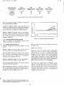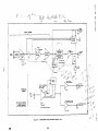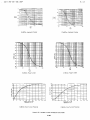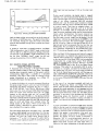
1
Jan-29-02
ll:43A
P.Ol
,
MODEL 124A
LOCI<-IN AMPLIFIER
OPERATING AND SERVICE MANUAL
.
"
-e-n~EGc.G PRINCETON APPLIED RESEARCH
MDl12<11A.; 3/n·QQ
[email protected]&.QPRiNCETONAPPt..IlDRESEARCH
Prtlt'lIJd In U.S.....
Jan-29-02
SHOULD YOUR EQUIPMENT REQUIRE SERVICE
A.
Contact the factory (6091452·2111) or your local factory
-aprasantative to discuss the problem. In many cases It
will be possible to expedite servicing by localizing the
problem to a particular plug-in circuit board.
B.
II it is necessary to send any equipment back to the faclory, we need the following information.
C,
P.02
11'43A
(1)
Model number and serial number.
(2)
Your name (instrument user).
(3)
Your
(4)
Address to which instrument should be returned.
(5)
Your telephone number and extension,
(6)
Symptoms (in detail, including control settings).
(7)
""01,,11' purchase order number tor repair t.ha,rges (does
not apply to repairs in warranty).
(8)
Shipping instructions (i1 you wig h 10 authorize shipmen. by any method other than normal surtaca
transportation),
ecoress.
U,S, CUSTOMERS-Ship the equipment being returned
to:
EG&G PRINCETON APPLIED RESEARCH
7 R(lSzel Road
(Off Alexander ROCld, East of Route 1)
Princeton, New Jersey
D.
CUSTOMERS OUTSIDE OF U.S.A.-·To avoid delay in
customs clearance of equipment being returned, please
contact tile rectory or the nearest factorv dtstnbutor for
complete shipping information,
E.
Address corr e spondence 10:
FG&G PRINCETON APPLIED nESEARCH
P 0 Bo' 2565
Princeton, NJ 085~.J
phone: 609/452-2111
TELEX: 84 3409
WARRANTY
EG&G PRINCEtON APPLIED RESEARCH warrants each tnstrument of its manufacture to be free 'rom detect s in material
and wcrkrnanshlp. Obligations under this Warranty shall be
limited to replacing, repairing or giving credit for the purchase
prtce, at our option, of any instrument returned. freight
pr'£"paid, to our factory wtthtn ONE year of delivery to the
original purchaser. provided prior authorization for such return
has been given by our authorized rapraaantauve.
This Warranty shall not apply to any Instrument which Our inspection shall disclose 10 Our saustecucn. has become deteclive Or unworkable due to abuse, mishandling, misuse. acctdent, alteration. f1egliger'ce, improper installation or other
causes. beyond Our control. Instruments manufactured by
cthera, and tnctuded in or supplied with OUf equipment, are not
covered by this Warranty but (:~HrY tne odginal rnanu tactur era
warranty which is extended to our customers and may be more
restrictive, Certain subassemblies, accessories or Components may bo specifically exctuded from tnts Warranty, ill
which case such exclusions are listed in the Inetructton
Manual supplied with each Instrument.
we reserve the right to make changes in design at any nme
without incurring any ohlig(:llion 10 install same on units
previously purchased.
THERE ARE NO WARRANTIES WHICH EXTEND BEYOND THE
DeSCRIPTION HEREIN. THIS WARRANTY IS IN LIEU OF. AND
eXCLUDES ANY AND ALL OTHER WARRANTIES OR RePRESeNTATIONS, EXPReSSED, IMPLIeD OR STATUTORY. IN·
CLUDtNG MERCHANTABILITY AND FITNESS, AS WELL AS
ANY AND ALL OTHER OBLIGATIONS OR LIABILITIES OF
EG&G PRINCETON APPLIED RESEARCH. INCLUOING. BUT
NOT LIMITED TO. SPECIAL OR CONSEQUENTIAL DAMAGES.
NO PERSON. FIRM OR CORPORATION IS AUfHORllED TO
ASSUME FOR EG&G PRINCETON APPLIED RESEARCH ANY
ADDITIONAL OBLIGATION OR L1ABII,.ITY NOT EXPRESSLY
PROVIDED FOR HEREIN EXCEPT IN WRITING DULY EXE·
CUTED BY AN OFFICER OF EG&G PRINCETON APPLIED
RESEARCH.
Jan-Z9-0Z
11:44A
P.03
TABLE OF CONTENTS
•
Page
oection
CHARACTERISTICS
Introduction
'_1
Specifications:
1.2
Signal Channel Specifications.
1.2A
Reference Channel Specifications
1.2B
Dumodul ator Characteristics
1.2C
Outputs
1.20
Dvnernic Rcmge Specifications
1.2E
Other Characteristics
1.2F
11·1
11-1
11-1
11-1
II
INITIAL CHECKS
Introduction
2.1
Equipment Needed
2.2
Procedure
2.3
III
OPERATING INSTRUCTIONS
Block Diagram Discussion
3,1
Introduction
3.1A
3_1B
Signal CharH"H:~1
Reference Channel
3_' C
Synchronous Detector
3_10
Signal Channel Operation
3.2
3_2A
Introduction
Preamplifier Choice
3.2B
Grounding
3.2C
Remote Preamplifier Adapter
3.20
Sinqle-Endsd, Differential. and Transformer Inputs
,,'3_2E
Common-Mode Rejection
:l2F
3_2G
Noise and Source Resistance
Selectiv@ Amplifier
3.2H
3_21
Dvnarnic Range
3_2J
Dvnamic: Over-ride
3_2K
Overload
3_2L
Offset Due to Noise
Overload Racnver v
3.2M
Signal Monitor
3.2N
Reference Channel Operation
3.3
Sync Input/Output
3,3A
'.3.3B
Phase Control'
...
»
Outpu t Channel OPeration
Filter Time Constant
Offset Controls
3_5
Harmonic Response
3_6
Sensitivity and Notch Calibration
3_7
AC Voltmeter Operation
3_8
Digit(ll Panel Meter Modification
3_9 "./ Phase Me aauremerrts
3_10
Rear Panel Connectors
3A
4AA
3AB
3,lOA
3,1011
3,11
3.12
)
1·1
1- 1
1-3
1-3
1-3
1·3
1·4
1-5
1-5
Interlace Connector (J9)
Ext. Time Constant
Flattery Operation
Phase Modification
111-1
111-1
111-1
111-1
111-1
111-1
111-3
111-3
111-3
111·3
111-4
111-4
111-5
111-5
111-6
111-13
111·15
111,15
111-17
111-17
111-18
111-18
111-'8
111-19
111-21
111-21
111·21
111-21
111-22
111-23
111-24
111-27
111-28
III-n
111-29
111-29
111-29
Jan-29-02
3.13
3.14
3.15
IV
P.04
11,44A
Mixer Monitor Mo<lifiCiil(ion
Remote Programming Option Modification
Selective External Reference Modification
ALIGNMENT PROCEDURE
4.'
4_2
4.3
4.4
4.5
Introduction
Equipment Needed
Procedure
4.3A
4.3B
4.3C
4.3D
4.5E
4.5F
4.5G
4.5H
4.31
Initial Reference O~cillator Board Adiusrmanrs
Auxiliary Reference Board Adjustments
Mixer Board Adjus tmenrs
lntermediate Amplifier Board Adjustments
Final Reference Oscillator Board Adjustments
Signal Board Adjustm@llts
Final Adjustments
4.3J
Phase Meter Option Alignment
Preliminary Steps
±24 V Adjustments IR6028 and R60101- Power Supply Board
Model 116, "7, or 119 Preamplifier Alignment
4.4A
Preliminary Steps
Procedure
4.4B
Model 118 Preamplifier Alignment
Preliminary Steps
Procedure
4.5A
4_5B
V
VI
TROuBLESHOOTING
5_1
I ntrod ucnon
Equipment Required
5.2
Initial Steps
5.3
5,4
Power Supply
Reference Checks
5.5
5_6
Signal Channel
Preamplifier
5.6A
Signal Arnplifier
5.66
Intermediate Amplifier
5.6C
Mixer Board AC Gain
5.6D
Mixer Schmitt Triggers
5.6E
Mixer Circuit
5.6F
DC Ampl tflers
5.6G
Noise Checks
5.7
SCHEMATICS, TABLE OF
111-29
111-30
11I·31
(
IV-'
IV-'
IV-'
IV-'
IV-'
IV-'
IV·3
IV-3
IV-4
IV-5
IV-5
IV-5
IV-6
IV-6
IV-7
IV-7
IV·7
IV-8
IV-B
IV-8
_v.t
_ V·l
. V-'
V-'
_ V·l
v-t
V·3
V-3
V-3
V·S
V·S
V·5
V-S
V·6
V·6
(
VI-l
c
Jan-Z9-DZ
P.DS
11:44A
FIGURES
»
Page
'.Imber
1-1
Model 124A Lack-In Amplifier
1·2
SYnc. Signal Slewing Rate
1·3
111-1
Typical Calibrator Accuracy
Functional Block Di.gram, Model 124A
111-2
Optimum Performance Regions of the Pre arnpfifier s
111·3
Distortion v, Frequency, Model 118
lirA
111-5
111·6
III· 7
11I·8A
111·86
Ground-Loop Voltage Heiection Using Di tferenttal Inputs
Model 183 Remote Preamplifier Adaoter
Typical Common-Mode Rejection
. . . . __ . . . .
Tvolca! Noise Figure Contours for Model t 17, Model 116 (Direct! and Model 119 (Direct)
Typical Noise Figure Contours for MOdel 116 Operatinq in the Transformer Mode . .
III-SA
Tvpicat Noisl! Figure Contours for Model 119 Operating in the Trans torrner Mode , .
Typical Amplitude Transfer Curves for Model 119 Operating in the Transformer Mode
111-98
111·10
.
Typical Amplitude Transfer Curve, for Model 116 Operating in the Transformer Mode
Typical Norse Figure Contour's for Model 118
,
, __
, ..
111·11 A Tvpical NoiSe Figure Contours for Model 190 Transforrner-Plus-Preamptitier
111-118 Model 190Wiring Diaqr arn
If l-t l C Tvpical Amptirude Transfer Curves for Model 190
111-11 D Photo of Model 190 Transformer
111-12 S-H Curves and Waveforms
111-13 Degaussing Wetveforr'J)s
111·14
Model 124A Bandpass Charac taristics
111-15
Model 124A Notch Characteristic'
111-16
Model 124A Low Pass Characteristics
111-17
111·18
1-19
111-20
111-21
111-22
111-23
111·24
Model 124A High Pass Characteristics
Dynamic Range Cnaracteristics of the Model 124A
Typical Output Offset as a Function of Input Noi,e
IV·l
Typical Reference Oscillator Slewinq Rate
Net Phase Difference Between Signal and Reference Channels as a Function of
Output Filter Transfer Function,
Tvpical Calibraticn Accuracy
_
Frequeucv
.
_
_
Mixer Output for In-Phase and Quadrature Signals
Model 124A Adjustments. ijlnrj Testpoinrs
1·2
1-4
1-5
111-2
111-3
111-3
111-4
111-4
111-5
111-7
111-8
111-8
111·9
111-9
111-10
111·11
111-11
111-11
111-11
111-11
111-11
111-12
111·12
111·12
111·12
111- 14
111-17
111-18
II 1·19
111-20
111·24
111-29
IV-2
TABLES
Page
Number
1-1
1·2
I" -1
111·2
,
111-3
111-4
111-5
11I6A
111·68
111-7
II 1·8
111·9
V-I
Praarnpfifiar Specifications . ,
, . . . __ , .
Model 124A Dynamic: Range Specifications
Stability and Output Noise as a Function of Operating Dynamic Tradeoff
Maximum RMS Input Levels for Mixer and Tuned Amplifier Overload as a Function of
Sensitivity and Operating Dynamic Range _
Maximum Frequency Acquisition iime$ of Oscufator .
Typical Harmonic Response Operating in the Flat M<'H.:I~
Typical Harmonic Res~onse Operatinq in Bandpass Mode with 0 - 10
Digital Output Pin Assignments
Digital Output Truth Tables
_
.
Interface Connector Signals and Pins
.
External Time Constent Connector Signals and Pins
Remote Programming Connector Pin Assignments
Gain and Relay Switching for tho Model 124A
. 1-1
_ 1-5
111- 15
111-16
111-19
111-22
111-22
111-25
111-26
111·28
II 1·29
111-30
. V·4
Jan-Z9-0Z
P.06
11:45A
SECTION I
CHARACTERISTICS
1.1 INTRODUCTION
The Model 124A Lock-In Amplifier accurately me asures
the rms amplitude and phase of weak signal~ huried in
noise. Signals in the range of picovol ts up to 500 millivolts
at freouencies from 0.2 Hz to 210 kHz Can be measured
quickly and precisely. Meter and voltagp. outputs are
provided for the amplitude, arid t1H~' phase of the signal m<1Y
be read from a dial. These measurements are with reference
to ~ wnchronjzjqg signal supplied to. or supplied by, the
Model 124A. In either the External or External f/2 mode of
op~ratiorl,
the instrument will accept any
above de, ,0 that the detector output is a de voltage
propor'tional to th~ in-phase component of the fundamental
signal. Propi:!r selection of signal channel and output
channel filtering parameters can render the final noise
bandwidth extremely narrow _ The rrns value of the [undamQrHal signal is indicated on the pal'l~1 mater when the
synchronous detection phase is adjusted for maximum
detector output.
A SWitch is provided that allows drift to be traded tor
dynamic reserve. In addition. an output de offset ff;!atul"I~; is
provided to allow higher sensitivity settir1gS for relatively
steady signals, These fe<1ture~ permit selection of the
optimum opcr atinq mode for each experimental situation.
rl?ferel~~
waveform that crosses its. mean twice each cycle, and will lock to
and track that signal OVC( a 100: 1 frequency range. In the
Internal mode, the frequency is determined by front-panel
dials or by an externallv derived voltage,
Other de:;igr"l fcaturas include selection of output filter lime
constants. to 300 seconds, optional digital panel meter with
BCD output, ij built-jrl calibrator. and independent use of
the phase-lockable oscillator and tuned amplifier for
general-purpose laboratory work, The Model 124A ","y
also be used as a conventional wideband laboratory
voltmeter.
A selection of ptuq.in preamplifiers is available for providinq optimum low-noise performance Over a wide range of
input frequencies and source resistances:, After preampll·
ficatton. noise and harmonics acccmpenvinq the signal are
attenuated in the Signal Channel by filtering out all
frequencies except the band in which the signal lies. Flat,
band Pass. band reject, high pass, and low PHSS filtering
modes may be selected. The remaining band of frequencies
is converted to an equivalent bandwidth about de by a
-vncbrrinous detector. which is locked to the svnchronlztnq
qnat. A low-pass filter elirnirlatEi!s frequency components
Accessories include an ac zero offset, several light choppers.
a computer interface system. and a wide assortment Of
low-noise preamplifiers.
Specification
Model 116
Model 117
Model 118
Model 119
Input Z
Selected by front panel switch:
Direct; 100 rneq, SEIDE
Transforrnere: Low Z SEIDE
100 meqohrns SEIDE
10 kilohm'S SEIDE
Selected by front panel switch:
Direct; 100 rneq, SEIDE
Transformer: Low Z SEIDE
Bandwidth
Direct; 0_2 Hz - 210kHz
Transfcrmerb: 1.5 H.z:-l0 kHz
0.2 Hz ..- 210 kHz
0.2 Hz - 210 kHz
Direct; 0.2 Hz - 210 kl-lz
Transtormerv. 1 kHl-210 kHz
Common Mode
Rejection Ratio
Direct: 120 dB at 60 Hz
Transformar: 140 dB at 60 Hz
120 dB at 60 Hz
1 10 dB at 60 H,
Direct; 120 dB at 60 Hz
Transformer: 120 dB at 60 Hz
Full Scale
Sensi tivi tv
Direct: 100 nV
Tr anstor mer: 1 nV a
100 nV
10 nV
MaximLlm Input
Voltage
Direct: i200 V de
tn mv rrns
sine wave
±200 V de
Direct; 100 nV
Tr ansforrner: 1 riV
±5 V
Transformer:
ay b. wired for 1:50 to 1:350 turn, ratio. Stand,,,d is 1:100.
"varies with source Impedance.
Direct: ±200 V de
Transformer; 10 mV rrns
sine wave
NOTE: A cur ten t-sensi tive preamplifier, Medel 184, is also
available. See ACCESSOR IES list at end of specs,
.
"
Table I.'. PREAMPLIfIER SPECIFICATIONS
1-1
t,
III
:l
I
N
Ul
I
o
N
SELECTS TIME CONSTANT OF OUTPUT
L P FILTER. S OR II dB / OCT" VE ROUOFF
SELECT EXACT CENTER
FREQUENCY OF SELECTIVE
.. MPLIFIER
'"'"
CRANII(S IN de OFFSET IN f'RONi OF
FREQUENCY RANGE
AOJUST FOR ZERO
TR"NSFER or CENTER
FREQUENCY IN NOTCH
MOOE
O'JTPLT AMPLIFIER. I TURN' I FULL SCA.LE,
FOR A Tcrr"L OF '0 FULL SCALES.
TOGGLE SELECT POL.. RI TY.
:t>
LI GHTS IF REf. OSC. 'S NOT
SELECTS sH A.RPN ESS OF
SELECTIVE A.M P LI FI ER
e<' lIto 13 dB
SELECTS OPERATING
MOOE OF SIGI>IAL
CHANNEL
-1>
U1
FREQ. LOC~ED TO REf. 'NPUT.
OQES NOT mo ICATE PHA.SE UNl.OCK
/OVERLOAO INDICA.TOR
... _-~
"'
-.-
/----
N
AVE~ AGE -
AEADJ NG
METER CA.L.lB;ftATEO
~N RM S FOR SlNE- WAVE.
If!lPUT
USEO 'WHEN
CALIBRATING
SiENSITlVITV
LECTS CA.L.
VOLTA.GE CAL.
IN BAN 0
PLUG-liN PRt:AMP'.
~
MODEL 116,I ~ 7, lie
OR 119. SELECT
ACCORDING TO FREe<.
RANGE ANO SOU~CE
'''PEOANCE. SEE
SPECS. MOOEL II S
INCREA5ES OVERA.LL
5ENS. BY l( 10.
~\'=:-" I'Q'r "- " O "' _ oUOO'
-.., ..
.-,_ _-...-.
.1',)\,
'W._.~.
@-
~
PASS
S WIT ... HIGH (l
..t.
'"
SELECTS 'OPERATI"G
MOOE OF OSCILLATOR.
IN "Z PQSITIO!',
osci LLATQFl' LUt,;:KS
TO SECOND IIAR"'ONJC
OSC. RANGE.
IN Ex:TERNAl
OECIMA.L
SELECTS INSTRUMENT
FUNCTION. IN AC FOSlnON~
POINT
MaOE SET TO
EXPEhEO RANG.~i
OS(;. PHA.SE-LOCI<>
.. CTS "5 W'QEB"NO RMS
VOLTIWETER. IN PSO
POSITIONS, ACTS AS
AU TOMATIC ALLY,
NULTI PLIEiR IN tNT.
SELECT PHASE OF SYNa-lRONOUS
,,REFERENCE INPUT TO
WHICH OSCILLATOR
LOCKS.
osc.
SELECT
E~"CT
esc: LLATOR
l..OCI<·lN
A~PlIFIER
DETECTlON wml RESPECT TO REI'
FREe<UENCY OF
IF OPERAn NG IN
LOC KS TO
INTERNAL MOOE. NOT F UNCll ONAL
POSITIVo-GOIPlG ZERO
WHoN OPERATI ~G IN o~1lERN"L o.IOOE
CROSSING
fig.," 1-1. MODEL 124.0,LOCK·IN AMPUflER
il
>
•
e
-
o
'-J
Jan-29-02
1.2
P.OB
11'45A
0.01%. The frequency stability is typically 0.05% of
the set freq\Jency.
SPECIFICATIONS
1.2A SIGNAL CHANNEL SPECIFICATIONS
-"
Frequency Aange
Model 124A; 2 Hz - 210 kHz
Model 124AL: 0.2 Hz - 210 kHz"
121 EXTE RNAL' The internal reference oscillator will
lock in both trequencv end phase to virtually any
extemaltv generated signal crossinq its mean onlv
twice each cycle. Maximum input voltage is ±20 V de.
Minimum time required on either side of the mean is
100 ns. Amplitude excursion must be at lean 50 mV
abovo an d below t he me en. rnou t i rnpedanee is 1
Sensitivity: 21 full-scale ranges in 1-2-5 sequence. Full-scale
vol taqcs are determined by the choice of pre amplifier ,
Ser~$it.ivity and all other preamplifier-determined specifications are given in Table 1.1. u
r'r'n~ go h rn.
When locked on, the raferunce oscillator will track the
external signal over a frequency range of l00~ 1 within
the range of the set band of frequeneie~. Ma.imum
frequency acquisition (lock-on) times for each frequency band are given in the following table.
Sign,,1 Channel Modes of Operation
(1) FLAT: Flat response within ±1% from 10 Hz to 110
kHz. ±2% from 110 kHz to 210 kHz. and ±10% below
10 Hz.
121 BANDPASS; Provide' a tunable bandpass response
with the center frequency set by front-panel digital
dials o,v" a ranqe of 2 Hz to 110 kHz. Setting
accuracy -is within 12% Or 0.05 Hz, whichever IS
greater. Bandwidth is adiustable over a rang~ of 1% to
100% (at 3 dB points). corresponding to a range of Q
between 100 and 1. by means of the front-panel Q
Xl
Xl0
Xl00
Xl K
XlO K
control.
(31 NOTCH, Essentially the same as the Flat mode, but
•
FREQUENCY RANGE
BAND
with the addition of a tunable notch that provide, up
to 80 dB of attenuation at any specific frequency. The
notch is tuned with the same controls as set the
bandpass frequency.
(4) LOW PASS, Essentiellv the same as the Flat mode,
but with the addition of a low pass. filter that provides
a 12 dB per octave rctlott a~)ove the set freqv(!'lCY.
.
.
.
.
.
0.2 Hz to 21 Hz
2 Hz to 210 Hz
20Hzto2.1 k Hz
200 Hz to 21 kHl
2.1 kHz to 210 kHz
MAXIMUM TIME'
.
.
..
.
.
15 minute,
2 minutes
10 seconds
2 seconds
2 seconds
Once the frequency hJS locked, the phase will track at the
rate shown in the diagram on the following page.
Phase Adjustment: Calibrated 10 turn potentiometer provides 0·100<) phase shift. Linearity of phase setting is within
±2 from 2 Hz to 21 kHz, and within ±5° from 21 kHz to
210 k l-lz. Resolution is D.1
A four-position quadrant
switch provides 901' phase shift increments.
(51 HIGH PASS, Essentiallv the same a' the Low Pass
mode, but with the substitution of a high pass filter in
place of the low pass filter.
Q
Q
•
1.2B REFERENCE CHANNEL SPECIFICATIONS
1.2C DEMODULATOR CHARACTERISTICS
Modes
(1) INTERNAL: Frequency of the internal reference
oscillator is set by means of fr ont-panat digital dials
and/or rsar- panel VCO control voltage, Setting accuracv is within ±2% Or 0.05 Hz, whichever IS greater.
veo control vcttege of 0 to ± 10 V corresponds to the
full frequency range on all bands. VCO input irnpedance is 10 k ilohrns. The amplitude stability is typically
ACVM; An ACVM position on the function switch permits
the Model 124A to be used as a convenrional or Irsquencvselective ac voltmeter. Accuracy is within ±1% from 2. H2 to
20 kHz, increasing to ±10% at 210 kHz.
Dc Output Stability and Noise' Dependent on the oper.ting
mode selected by the front-panel Function switch, as
shown in the Stability & Noise Tobie (next pagel.
° Modtill 124AL h;]5 5igrlifi!:::;!IlltIV lunasl' severe-over toad reCO\lllrv
nme (80 s n 30 5 with ~OOO limes 1ull $clIle OV8,IoOid for onljl
""'11'l1J~el .
•• Two additionOiI prel ...rnplifier5. t h e Modal lB4 ;lind thll Modilll 186,
£Ira evauetne. r-or informatIon, c oo tac r (118 hlctOrV or the eecro-v
"Timl!l cOIn bll $hQrtanl;td .!I~p(ecillbIV by r~lUmelHlIl'ily switehino (0
lntl!lrnollli Modll IjInd rnal'llJll!llIy 1-ettir"lQ thE! csc Hta ror to ene pr eper
re~r65ti1rHlItivl!!r in vo ur IIrl!rll.
're~uencY.
1·3
Jan-29-02
P.09
11'46A
"o~
o
,."
(
00'
l'.5
.
."'
.
~
-,
o·
!il
-O<f.
w
."
~
•
-180
-0,004
-0,003
"'0
-0.'
-0,3
-O·~
XIOO
-.0
X"
..
-30
-
-30
XI
.. ..
.z'"'".
-O·QO~
0.002
0
0.001
- 0.1
0
0,1
O.~
0.3
0.'
-'0
-'0
0
'0
~o
30
'0
-h
-"
0
,.
~.
•••
."
~O.OOI
0.003
0.00"
~
z ..
........."""...
"II:
""
""
"
.
~
,,~
XIOII
.. 11S'
SY~c.
""32.
$IGiU.L
-44t
"IU
SLEWINt:i
,u.Tf:
I
0
Hi: I SE;CO-'O
..
l!Jh
••
1711!i1l:
Figurl!ll-2. SYNC, SIGNAL SLEWING RATE
Function
Output Stability
LOW DRIFT
<150 IN I "c
<1 rnV/"C
<10 mv / "c
NO~MAL
HIGH DYN RANGE
Equtvute nt Noise Bandwidth: 416 ,u:Hz minimum (300 s
time constant with 12 dB/octave rolloff).
<100J.lV rms
Zero Suppress: Calibrated control permits off-setting zero
by ".1000% 01 lull scale on Normal and High Dynamic
Rang. only.
<1 mV rms
<10 mV rrns
•
System Gain Stability; 100 ppm/ aC; 100 ppm/24 Hr in the
Flat mode and with Function switch set to NORMAL.
Demodulator Overload Limits: Dependent on Function
switch setting as follows (see Subsection 3.21 for over-ride
conaider at ions).
1-20 OUTPUTS
10 x lull ,cal.
100 x lull scale
1000 x lull scale
ME!ter Redding: Choice of either center-zero or lcf thandJP.ro panel meter of taut-band construction. providing 0.5%
linearity.
This limit is defined CIS the ratio, at 1I~(! input. of the
maximum pkpk voltage of a non-coherent signal, before
overload, to the pk-pk voltage of a full-scale coherent
slnewave. Note that, in terms of pk-pk noise to rms Signal.
the instrument will accept. without overload, interfering
Signals having E1n amplitude up to 3000 times the sensitivity
sc ttinq, (See discussion in Subsection 3,21.)
OPtional Digital Readout: file Mo,I.1 124/\ may b. ordered
with an optiunal diqit al readout in place of the standard
panel meter. TIle readout is a 3% digit display with a
linearity of 0.05% of the reading, ±1 count. In addition, a
BCD output is provided at the rear panel. The output levels
are DTLlTTL compatible: Logic 0 = +0.2 V ±0.2 V, 5 mA
maximum sinking current; Logic 1 = 4-3.5 V ±l.O V, 100
flA maximum sour cinq current.
LOW DRIFT
NORMAL
HIGH DYN RANGE
, .. , .
,.
,
.
.
Filter Time Comt;jlnb: 1 ms to 300 s in 1-3-10 sequence.
and a mi nlmum time constant posltlon having a time
constant of less than 1 rns [daterrruned by internal stray
capacitnnce}. n1E~ External position allows capacitance to
be added via a rear-panel connector" to obtain special values
of time constant. Either 6 or 12 dB/octave rollotf as
selected by means of front-panel switch is pr ovtded.
Function Out; A de signal corresponding to the panel-meter
rcadinq, An output of 10 V corresponds to full-scale
deflection. 'The output impedance is 1 1<>11.
Signal Monitor: Enables continuous monitoring of the
signal channel output ahead of the demodulator. In LO
DRIFT operation, a full scale rrns input sfnewave gives a
100 mV rrns sinewave at the Signal Monitor jack. In
NORMAL operation, the signal monitor output with a
full-scale input is 10 mV. and in H I, it is 1 mv. Dvnernic
- MI!.".uured with li''''''1iiI (,QI"Ist.mt of 1 S Itnd 12 dl3!OCTilv\llulloff,
1-4
(
Jan-29-02
11:46A
P.I0
Output
Operating Dynamic
DYna(r'li~
Range Tradeoff
Range
PSD
Dynamic Reserv'!!
6_6 X 10"
LO DRIFT
NORMAL
HI DYN RNG
[Reserve]
10'
10 3
PSD
Dynamic Range
6_6
10
10'
10'
x
Total
Dynamic
R.iUig~
6_6 x 10'
10'
10'
10'
10'
10'
Table 1-2. MODEL 12.11A OYNAMIC RANGE SPECIFICATIONS
Over-ride considerations apply as explained in Subsection
3.21. Output impedance is 600
n.
.'"
Internal line frequency pickup is less than 20 nV rrns
(referred to the Direct inputs of a Type 116 Preamplifier)
in any Signal Channel mode except Bandpass and Notch,
where the level may rise to 500 nV at highest 0 settings.
;!
··
•
e 10
C
1.01
'±10
?
~
Hefarance Channel: A sinewave output at the reference
oscillator frequerlC.~V. Amplitude is. contmuouslv adjustable
by means of the front-panel Level com-o! over a range of
o V to 10 V rms with less than 2% distortion. Output
impedance is 600 ohms.
i
!O,l
0'
.'
,,'
~.
fi9ur'J 1-3. TYPICAL CALIBRATOR ACCURACy
1.2E DYNAMIC RANGE SPECIFICATIONS
Vary as a function of the operating Dynamic Range
Tr edeoff as indicated in the table above.
)
Size: 17-1/8" W, 7" H x 18-114" 0 (43.6em W, 17.8 cm
H x 46,5 em DI.
..LF OTHER CHARACTERISTICS
Overload: Front-panel light indicates overload at critical
circuits.
Weight: 34 lbs 115.5 kg!.
Reference Unlock; Front-panel light indicates that the
reference oscillator has not completed Irequeucv lock.
Accessories: Model 173 AC Zero Offset provides square
wave at the reference frequency which can be used to
suppress siqnals at the input of the Model 124A_ Other
accassoriss include a computer interface system, fixed and
variable: speed Iight choppers, and a broad selection of
special purpose pre ampfttlers. The AM-1. AM-2. and 190
input transformers allow better noise performance to be
achieved when ~Jsing a hiqh-input impedance preamplifier to
process a signal arising in a low source impedance.
Internal Calibr.ator: Square-wave calibrator signal supplied.
Rm5 amplitude of fundamental frequency component
sdjust atuc from 20 nV to 100 mV in 1-2-5 sequence.
Tvpical accuracy indicated in
Figl.Jr~
1-3.
Ambient Temperature Range: Unit can be operated at
ambient temperatures ranging from 15°C to 45°C.
Auxiliary Power Output: Regulated t24 Vat uo to 100 mA
The Model 184 Current-Sensitfve Preamplifier is also
available. This prear'r1~)lifier. which plugs i" like the Models
116. 117. 118. and 119 Preamplifiers. provides 1 V out for
input currants ranging from 1 nA to 10 J.1A <IS selected by a
tront-pancl Range switch, Frequency range varies with
sansitivitv, bC!ing:;'> Hz to:3 kHl on the 1 nA ranqe and 2 HT
to 200 k l-la on the 10 IlA ranqe.
is available at rear-panel connector,
105-215 or 210-250 V; 50-60 HI;
unit can also be powered from batteries. by supplvinq t31 V
Power Requirements:
to rear pdnel connector.
Bi:ltterie~ must
least 400 mA at +31 V and 360
,~A
be able to supplv at
at -31 V.
anu
eootv
ThA'l;II ./:If'1 maxrrnu m values
do nut
ro r ~II
the SenSITivity swttcn. for 8 g",n",ral (hii(:~Jjj.~lon of yhll
rTHHllning at these ter ms IlI"IIJ Hllllllr Ilgnifil:;<lnce, ~ee Appendix A A1t thl!
"NOT!::::
POSI~Il)nfj. 01
,IISf
Of thl~ manual, ,A I so. Gee Subsllllcticrl 3.21.
1-5
Jan-Z9-0Z
•
P.II
11:46A
SECTION II
INITIAL CHECKS
2.1
INTRODUCTION
Reference Frequency range: X100
Reference Mode: INTERNAL
Referonce level: 10 (cal.)
The followir19 procedure is provided to facilitate initial
per tormance chocking of H,e Model 124A. In general, the
procedure should be performed after Inspecting the inUr'I.JI"l)frH for
Phase potentiometer: 90 (9 full turns)
Q
Phase switch: 180
shippinq damage (any noted to be reported to
the carrier and to Princeton Applied Research Cor'pnratlonl. but before using it e xpenmentallv. IN THE CASE OF
UNITS HAVING A DIGITAL PANEL METER, IT IS
IMPORTANT THAT THE PHRASE "meter lull scale" BE
PRDPERLY INTERPRETED. READ THE PARAGRAPH
BEGINNING WITH "In reading tho display ---" ON PAGE
111-24 BEFORE PROCEEDING WITH THE INITIAL
CHECKS. Should anv difficultv be encountered in carrying
out these checks. contact the factory or one of its
authorized representatives.
Function switch: ACVM
Calibrator switch; 1 mV
(6) Connect a cable between the Calibrator BNC iack and
the preamplifier's A input.
(7) Turn the Power on and wait five minutes for warmup.
NOTE~ In an actual measurement application, allow
one 110ur warmup for optimum performance.
18) The Meter should read to tho right.
2.2
(91 Set the Signal Mode switch to BANDPASS.
EQUIPMENT NEEDED
(1) General-purpose oscutcscope.
(101 Adjust the rtqht-most Signal Channel Irequency dial
for a peak on the meter [approximately lull scale].
(2) Oscillator, having any 1 kHz repetitive waveshaps that
crosses its mean cxactlv twice e ach CYcle and having a
pk-pk voltage anywhere between 100 mV and 3 V.
(11) Switch the
(31 Assorted BNC cables.
2.3
°
switch back and forth between 100 and
10% ENBW positions, end adjust the Notch (frontpanel screW(:Iriver adjustment) for minimum change
betwear the two positions (less than 1% of F.S.
change). After adjusting, leave the Q at 100.
PROCEDURE (for digital units, see
page 111-24 before proceeding)
(12)
NOTE: This procedure must be performed in sequence.
set
the Sensitivity ADJ. potentiometer [fr on t-pane!
screwdriver adjustment) for exactly full scale meter
indication.
(1) Install a preamplifier if not already installed.
(13) Sot the Signal Mode switch to NOTCH. The meter
should now indicate 40% ±1S% of positive full scale.
(21 Check the rear-panel 115/230 switch. Make sure the
number showing in the window corresponds to the
line
voltag~
to be used.
114) Set the Signal Mode switch to LOW PASS_ The meter
should now Indicate 90% ±10% of positive full scale.
(j) Turn the front-panel Power switch OFF.
(4) Plug
(151 Set the Signal Modo switch to HIGH PASS. The mete,
should continue to indicate 90"A. tlO% at positive lull
scale.
(5) Set the front panel controls as follows.
(16) Sot the Signal Mode switch to BANDPASS.
the line cord into the rear panel and wall
racsptacles.
M!tf!r: Check mechanical zero. Adjust if necessary.
Preerrtplifier Input: DIRECT (if applicable)
This completes the Signal Channel checks. The Phase and
Function checks. follow.
(17) Set tho f unction switch to LO DRIFT.
Sensitivity switch: 1 mV {if uainq a Model 118
Preamplifier, set the Sensitivity switch to 10 mVI
(181 Set the a Selector to 10% ENBW. Then adjust the
Phase pctenriomc rar for zero on the meter. Lock the
potentiometer.
.
Signal Channel Mode: FLAT
Signal Frequency dials: 4.05
Signal Frequency range: X 100
a switch: 100
'r.me Constant: 300 rns
(191 Set the Phase switch to 270
0
•
Adjust. if needed. the
Zero Offset potentiometer: fully coun terclockwisa
Sensitivitv screwdriver control for plus full-scale meter
10 X Full Scale switch: OFF (center pcsttionl
indication.
PreamplifJer Mode: A
Reference Frequency dials: Red, NORMAL, Digits,
4.05
1201 Set the Phase switch to 90
minus full-scale 12%.
fl·,
0
•
The meter should indicate
Jan-29-02
P.12
11,47A
Calibrator output to 100 mV_ The meter should
remain at full scale ± 1%. NOTE: Calibrator to 10 mV
with Model 118 Pr camphfier.
(211 Set the Ph ase switch to 0·. The motor should indicate
ZCfO 12% of full scale.
(22) Set the Phase switch back to 270
indicate positive full scale ± 1%).
(231
0
•
(The meter should
(31) Pr oqressivefv rotate the Sensitivity and Calibrator
switches one position at a time, in a count~rl:;Ic.>r.kwiS'.e
set the Function switch to NORMAL. The meter
should remain at positive full scale (t.l%).
direction. The meter should remain al full scal. ±2% if
the two switches are in Cor(e~ponding positions. If the.
meter wavers too much in the low nV aet tinqs,
increase the Time Constant to 10 seconds, (If using
the Model 118 Preamplifier, remember that the
instrument is. 10 X more sensitive than is marked on
the Sensitivity switch, and set the switches accordingly, Just he sure to check all sensitivities for which
Calibrator volt.gcs are available.l
(24) Set the Function switch to HI DYN RANGE. The
meter should continue to indicate positive full scale
(±1%)_
This completes the Phase and
Reference Channel checks follow.
Function checks.
The
(251 Connect the Signal Generator to the Referenet! Chennel's In jack. The pk-pk voltage "an be anywhere
between 100 mV and 3 V. Set the signal generator's
frequency to approximately 1 kHz.
This completes the Sensitivity Range checks. The Output
Offset end Overload checks follow.
(321 Remove the Input signal to the Preamplifier.
126) Monitor the Reference Channel's Out jack with the
oscilloscope. The waveform should be a 28 V (i2 VI
pk-pk slnewave.
(33) Set the Time Constant switch to 300 ms.
134) Set the Sensitivity switch to 1 mY.
(27) Set the Frequency Mode switch to EXT. The Ref.
Unlock light should come on. Observe the frequency
135) Place the 10 X Full Scale <witch to "-".
(36) Adjust the Offset potentiometer for exactly one turn
clockwise. The meter should indicate positive full scale
of the oscilloscope waveform. It should have bcqun
increasing as soon as the Mode switch was set to EXT.
After several seconds. it should stop increasing. When
it stops. the Ref. Unlock light should go out, (The
me ter will go to Zero also.I
IZ81
!2%.
(371 Place the 10 X Full Scale switch in ".". The meter
should nnw indicate negative full scale ±2%.
NQ~l:!: 01C trequcncv of the o$cillO$cope waveform,
Then place tho Reference Mode switch to f/2; the
freql,.l~r'CY should double.
(381 Increase the Offset potentiometer setting to 1_6 turns.
The Overload light should come on.
This completes the Reference Channel checks. The Sensitivity Range checks foliow.
1391 Bc tur n the 10 X Full Scale switch to its neutral off
position, Ths Overload light will go out.
(291 Set the Reference Mode switch back to INT,
completes the Initial Checks. If the instrument
performed as indicated, one can be reasonably sure th at it IS
operating properly.
(301 Set
both the Signal
Channel Sensitivity and
This
the
11-2
Jan-Z9-0Z
•
P.13
11:47A
SECTION III
OPERATING INSTRUCTIONS
3.1
The Intermediate Amplifier is ac coupled, thereby eliminating de drift problems in the Signal Channel.
BLOCK DIAGRAM DISCUSSION
3_lA
INTRODUCTION
discussing the actual operation of the Model 17.4A,
let us e'l;amirll:! a functional block diagram to bette r
understand what each adjustment does, and how the
various adjustments relate to or influence one another. The
functional block diagram i$ IQc.:';H~d on the following page.
Schematics and a chassis wiring diagram ere included at the
back. of this manual.
Bef()r~
The Synchronous Detector is the heart of the instrument.
around which are situated the Signal Channel, the Reference Channel. and the Output Amplifier. The Signal
Ch annal amplifies and filters the siqnal, clnaning it uo as
much as possible before passing it along '0 the Synchronous
Detector. The Referel1ce Ch(i"r'Iel controls svnchronization.
3.16 SIGNAL CHANNEL
Preampljfle r
Four models of plug-in preamplifier' arc available: the
Model 116, the Model 117, the Model 118, and the Model
119~_ Together they cover the whole frequency spectrum
from near de to 210 k Hz , each model having the best kind
of input circuit for optimum tow-noise performance in its
frequency range_ The Mndel 116 may be considerec the
qeneral-purpose choice, performing well in most situations.
Specific data for the four preamplifier models Is given in
the specifications in Section I and in the discussions in
Subsection 3_1.
REFERENCE CHANNEL
Voltage-ContrOlled Osclllator
The VCO either locks onto a svnchronizinq signal from the
e)(periment, Or provides iii: $Vf'lchroniling signal to the
experfrnent. The Vee drives the Syr,dlfonOllS Detector so
that the e xpertment an(1 the Model 124A are properly
synchronized.
The VCO automatically phase-locks to any kind of reference waveform hoving a frequency within approximately
two decades of the Hcfe rc nce Channel band setting. the
only requirements heing that the waveform cross the mean
twice {only I each cycle, that it have a pk-pk amplitude of at
least 100 mV, and that it be svnchroriized with the signal of
interest. The vee can also lock to the secono harmonic of
the reference ~ign,al, if desired.
I~ is important to realize that, even though the VCO will
phase lock over a two decade frequency range, the
boundaries of the lwu dur.ades an~ determined by the
setting of the O~r:iIlMnr Ranqc switch. The tracking range
corr espondtoq to each po sition of the switch is as follows.
Xl
,.""".""
_ . _ .. __ . 0.2 H, to 21 Hr
XlO
,.",.""".,,_,
.
2Hlto21OHI
X100 , , , , .'
__ . _.
.. _20 Hz to 2_1 kHz
X1K " " , ,
.
._.
200Hz!o21 kHz
XlOK
, .. , ,
2 kHz to 210 kHz
In the Internal mode. a sinewavc OLltPut from th~ Oscillator
Selective Amplifier
The Selective Amplifier functions as a variable 0 filter,
which l"Iiay be operated in the high-pass. low-pass, notch,
bandpass, or flat mode. Because rrns noise amplitude is. a
direct function of bandwidth. much of thl!: noise can be
rejected in this. stage by filtering out all but the band
cont aininq the wanted signal. In addition, odd harmonics,
to which the Synchronous Detector is sensitive, clin be
eliminated.
,
3.1C
is provided for synchronizing the experiment. The Oscillator can free run accurately at any selecled frcqvency from
200 mj-iz to 210 kHz, Also, the Oscillator's frequency may
be controlled by a voltage applied to a rear-pane! jack.
Phase Controls
The Phase Controls combine quadrature outputs from the
VCO such that the resultant sinewavs presented to the
Svnchronous Detector' has the desired phase relation to the
reference (sync input and/or output).
Intermediate Amplifjer
The Intermediate Amplifier provides additional gain so that
the siqnat-p lus-ncise applied to lhe' Synchronous Detector is
as. large as possible without overload. Presenting ~J larqe
signal to the Synchronous Dete cror minimi ....es. for a given
everett senstrivitv. the noise and de drjft contributed by the
Outp ut Channel.
3.10
SYNCHRONOUS DETECTOR
The Svnchronous Detector inverts the polarity of the part
of II"Ie input signal ccr respondinq to the naqativc excursion
of the phosc.stutted sinewave from the VCO. and passes the
remaining waveform uninverted. Therefore, the de cornponent of the resultant waveform is proportional to the
value of signal at the same frequencv and phase as the
phase-shifted
sinewave. Because the detected signal
still has noise on it. RC low-pass filters that follow the
svnchrooous detector are used to eliminate ull but the de
component rspresentinq the wanted signal. A de ampllfier
"AI!;!;) avaIlable cr e the Mod~1 184 Photorn~trjc Preampldler Il ....d the
1135 Sirlgle·Erldec1 Low Nctee PreamplIfier. The:~e two
preampl,f,e(! ware devlllioped laul:( m an the prU;:IrnlJllflers dj!lt:U5S~d
in thl!> manual. FOr infcrm,UIOn I!Ij~d slJtlcific",tionl;', contact the
factory. Seoarare instruc:tion m811UI!IIIs lire prQvidet;l for the Models
veo
Morlel
184 and 185.
111·1
t,
III
:l
I
F
I
" .tJ)
).)I -...;..,
W
TE-5J Sc..++ uK-\
,
o
I
o
1 .'
l-·~
r-,
N
M '1-' -T'-~"J
o
..
U1
r---------------T.......,..'" J
0_
A ......
~
./
,
SIGNAL CHANNEL.
C\
=0'
N
.J>
il
~ '0''''
on
o-£T£CJ1JiII
,..'-0;
.;...l..I'
.(.
• ...ODI::
.. f"I'IEQUEP,!C ....
'0
Sl~"
~
"","IS
• .... ODE~ IHi
.. QI'
<, <,
I It
".po I 18
IX
-i
~
'> ,
G) ~~Pvl
,,
..eli"
~SOI~;IY1 v 1T "
O('ECro-R
I
--TIME: CONSTANT
,/
"l"(II(I WF'PAESS ""./"
or
,
.............
=
.............
N
~
- i1'"
.-----.
VOLTAGE
"'7
F'HA5£
',i
""
(-' Or ~
.•
\ ..X'
Y " , J V·'
,
A· D..'-' " . 'I.'."\ "\ :_"'~
tI,.,.r
<a<ll<1S
j
, r;:.
~
-=
.2JO"
"'OUT
,"tl
.".
.
.
'.
..-
o'
(
UII~
I
,
"
or
~
,.-;,•
!.
\
·0
"'CAL_ L.[vtL
-=
l·t..r~
'j
•
.t'
.'
:l(
<t
CALIEllIiU.TOJI SQU,loJIIIE
'III"VI[ !ion
.....[F. lJI'Il.OClI; II'I00oC-ILTOiII
.t. >l
J I. I
<"l
''IT£No...rOA
.J"FI!EOJ;[ IIIC"f
~
I.e' \ i
,
CALII!IRaTOR' .[lIIlr¥lEiII
.
.
1
L'
- ..OO(
.
r.
100 tl
--L.E:'o'EL
"
:u
....IE oolFvr
:S~NC
,....NEl. COtITROL
' -1
~, ..0:..0
-<:OHIAOLL.ED
iREFER£NeE
l
,
S"fN(. SINE
f'ootI,I,S(-L-D::lIlo[O
CMANNEL
I
,
- ,':,'1
SYNC DRI'o'f1l'
"PII,D,nKNuAlCfr
OSCILL"TQIll
.. INOl'CATES FRON r
,
. v ...
-~."
J
. . .t;FIJ"ICTION"'/
r
,
"'.....
.-l-:-'- ~~;;~t- -- - -- -- - ----- .
1"1)r[1'!I
,
r,
~
.J.~l
,.;
~
Fig"" III~'. FUNCTJONAL BLOCK OIAGRAM. MODEL t24A
...
-
,
,I.'I
il
>
o
'"
Jan-30-02
05:24P
P.02
he at, etc. The chopninq frequency range must be fairly well
following the Detector provides the finesl gain. This amplifier drives the output connector and panel meter.
known, and sync sigr\als must be aViJilable. Of course, the
frequency of interest may not be a result of chopping at all.
The: chopping technique discussed here merely serves as an
exampl•.
To daterminu the amplitude of a signal. the operator simply
adjusts the phase controls for maximum meter indication.
The meter directly indicates the signal amplitude. In
addition, after making thil adjustment. the phase of the
input signal relative to the reference may be accur etelv
3.28 PREAMPLIFIER CHOICE
Four models of plug-in ureampltflers are available. each one
providing optimum low-noise performance over a given
input-resistance v, frequency ranqe, as shown graphically in
Figure 111-2. Two of these preamolifiars can be operated
both in direct and transformer-coupled modes, and all four
of them can be operated single.ended or differentf allv, A
Model 190 transformer can be used with any of the plug·ins
to improve low-frequency performance when working from
low source impedances. Use of the Noise Figure contours is
discussed in Subsection 3_2G.
r~ao
from the Phase dial.
3.2
SIGNAL CHANNEL OPERATION
3.2A INTROOUCTION
The function of each control is indicated in Figure 1-1.
Instead of repeating the intormatlcn qiven there, this
subsection provides additional background information for
setting the controls to their optimum positions.
Another consideration in selecting a preamplifier is its
ability to amplify without distortion. If an experiment
requires measurement of low level harmonics in the
presence of a high level Iundarnentat, it is important that
tho preamplifier not add significant harmonic signals by
non-linearly amplifying the fundamental. Except in the case
of the Model 118 Preamplifier, the distortion generated by
preamplifiers operating in the direct mode is so small as to
be unmeasurable using conventional methods. The Model
11B tan, h owever, distort more und~r certain conditions, as
indicated in Figure 111-3. In the transformer Mode, both
phase shif~ and distortion must be measured for each
individual operating condition.
To set I,JP the Signal Channel controls, the operator rnusr
know the frequency or frequency range of the signal. It also
halps if he knows the expected amplitude, the amount and
tvpe of noise obscuring the signal. and the signal-source
impedance.
The stimulus to the expsrirne nt is often chopped, Detecting
at this chopping freqi...encv eliminates all but the signal
related to the stimu Ius. Princeton Applied Research Corporation manufactures several models of light chopper which
are ideallv suited to photo-detection applications. Chopping
the source light finds its analog for other kinds Of
experiments i n chopping the stimulus de. ri, ac, sound,
10'
11$, II ", .. 1 1 9 - - - "
10
tllll'Eer IIIQfI[
I;URY!$ 1111142: APPLY' FQR ALL MODEL 1Z~ $~SITlVITY-p$(J
SETTING COJolelNATIONS EX"CEPT: p:Sc_ LO DR, SEN ~
10 ~V UHl,i -'00 ",Vi f1'S D & NO~MAl, SEN ~ 1 roY Ihrll
W
'00 e v ; j!I!iD _I'll DYN RNIJ, $£N .. l00 pY ",," "'00
"OR il'1ESf
10'
COM~INATION:S, CURlifS ~o1l1;!4 APPL....
;!.
":.;
"'v
~~
'.0
e ev
~.
;:
"t;
Q
Ci
110
~
.
'::~
Q
'0'
:;.
II
100 roY
10
10'
1ft 1/.
-I
10
zo "'v
J~
i!a.
~
I
~1
~~
;;:i
tnt;;
..
~t.
10
10
10.11
10"
10'
,R!QuENCV. Hz
~
~
Figure 111-3. DISTORTION v. FREQUENCY. MooEL 118
10'
'0
3.2C GROUNDING
In any system processing low-level signals, proper grounding
to minimize the effects of ground-loop currents, usually at
the power frequency. is an important consideration. With
the exception of the Models 184 and 185, all of the Model
124A preamplifiers allow both differential ar\d single-ended
opaearion. Two properties of these nraamofitiers allow
them to achieve a high degree of immunity to qr ound-f onp
currents. In differential operation, their extremely high
ccrnmon-rncde rejection (:l.SSUI'es an almost t otal rejection of
10
1.0
10
JQJ
'lOt
I'''EQUI!NCY. HI
Fig!,..... 111.2'. OPTIMUM PERFORMANCE REGIONS
OF THE PREAMPLIFIERS
111-3
Jan-30-02
P.03
05:25P
unwanted signals which appear at both inputs. at the sama
phase and amplitude, the usual Case for ground· loop
Impedance matching of the source and loading considerations often require that the input impedance of the
preamplifier be known, HOMVer. do nat confuse impedance matching with optimum input impedance for lownoise operanon. The latter is discussed in detail in
inter tnranee. In sinqte-endert operation, their unique input
gro~.lr'Idin9
system, in which signal
yround "tloats" off
chassis ground by ten ohms, assures a high degree of
rejection. As a result of this ten ohm grourld. ground loop
signals <.JrIJ efFectivelv attenuated by the ratio of ten ohms
to the braid rosisteoce (typically 20 mill of the c able
Subsection 3.2G.
The input impedance at each preamplifier (direCt model is:.
Mo<:fel 116,100 rneqohrrs 20 pF; Model 117, 100 msqohms
20 pF; Model 118, 10 kilohm' 170 pF; Model 119. 100
megohms 7.0 pF. These impedances are for each input to
ground. In the differential mode. for all models except the
118, the impedance from input to input is twice that stated
(; .e., R double, C heltl. For the Mod.1 118, the input
impedance for the differential mode is about the Same as
the jrnpeuance for single-ended operation. In addition, the
ditt. input impedance at tile Model 118 varies with
sensitivity and the setting of the PSD switch Icomrnonmode input impedance is 25 kO for all combtnattcns l. In
the Lo Dr;ft mode, on the 10 mV through 500 mV
sensirlvltv ranges, the input impedance is about threa times
that specified. In tIH!' Normal mode. the higher impedance
applies to the 1 (nV th rouqh 500 mV ranges, and in the Hi
Dynamic Range mude, it applies to the 100 IlV through
500 mV ranges,
carrying the sign(:ll from the source to the input.
.•,
GI'OUIUI LDOI'"
I;UIIlIII'![fIIT
...
IIllP.lI;"~
(lIl."lhhllll
"",_III 110"110 I
Figu,01ll·4, GROUND-LOOP VOLTAGE REJECTION
USING DIFFERENTIAL INPUTS
For the preamplifiers haviog internet transformers, the
Input switch operates the same for the transformer as it
does for direct, The Input impedance is very low in the
transformer mode.
Despite the immunity granted by the ten-ohm ground, far
better rejection can he achieved in processing a $iglliiill from
a single-ended source if one operates differentially as shown
in Figure 111-4. In single··ended opcr ation, the preamplifier
"sees" the potential difference between the center conductor of the cable and the braid, and ~rlY ground loop
sign~1 on th~ braid can be attenuated but not rejected
altogether. In differential operation. the preamplifier "sees"
the potential difkrence between the "A" Input and the
"B" Input. Ground-loop signal current flowing in the braid
is of no consequence.
HOWC!V!J'r. whan operating differentially, it is important to
assure that cornrnon-rnode interference arising in ground
loops is just that, i.e., without a sigllifiC.i;lnt differential
component. This should not prove OJ problem as long as
both sigr1al cables are the same ler)g1l1 and follow the Same
path.
-:
3.20 REMOTE PREAMPLIFIER ADAPTER
In situations where very low signal levels are encounrsred, it
may be desirable to operate the preamplifier very close to
the signal source to reduce noise and strcv pickup, while
leaving the main Lock-In unit ~t a convenient opcr atinq
location. This rnav be accomplished with the accessorv
Rarnote Preamp Adapter, Model 183 (see F;gu,e 111-5).
3.2E
SINGLE-ENDED, DIFFERENTIAL,
AND TRANSFORMER INPUTS
All of the preamplifiers have switch setnctable single·
ended/differential lnpurs. The differeMial inputs can be
used to combine siqnals (A - B) as well as 10 provide
common mode rejection.
Figure 111-5_ MODEL 183 Rf:MOTE PREAMPLIFIER ADAPTER
111-4
Jan-30-02
OS:2SP
P.04
If an external transformer, SI,H;h ~$ the Model HJO, is used.
is connected to the preamplifier single ended. The
ansf'orrncr alone provides sufficient common-mode r@jec-
The total output noise rnav be converted to an equivalent
input noise by dividing by the amplifier gain_ The noise
figure, expressed in these terms, becomes:
it
lion l~igure
III-Eil.
(2) Noise Figure =
2010
IJ10
Each amplifier has its own characteristic noise figure. which
varies as a function of frequency and source resistance.
These figures are obtained e xperimentatlv and plotted
graphically. Figure, 111-7 through 111-11 include typical sets
of noise figure contours for the Models 116, 117. 118. and
119 operating in direct and transformer modes.
z
o
"•
U
Ita
~
z
-•
~
c
•cz
Using the applicable set of contours, the total equivalent
rms input noise can be de terrnined:
,
c
,
is
!
f--,L---+-
100
"
I
ll !!
n.
Ii • ~oo'
eoecr.
I".f.~I.
Go,n
)
ee I---------.j---
rrns input noise voltage
thermal noise" antilog NF/20 volts rms.
(3) Total equivalent
I
,
<i"'IQ
117, II
!II (ll1iI'(cr
'I
.0
'"
Notice from these equations that the bandwidth must be
specified: usually determined by the external circuitry
and/or the amp lifisr bandwidth. Figure, 111-7 through
111·11 include response curves of the preamplifiers from
which the bandwidth may be obtained (in the direct modes,
the bandwidth is wider than the widest Tuned Amplifier
Bandwidth). However, a more interesting place to determine noise level is at the output of the Tuned Amplifier.
Because there is gain ahead of the Tuned Amplifier. its
noise contribution referred to the input is negligible
compared to that of the preamplifier. In computing the
total equivalent input noise of the signal channel, the
operator only need use a Af as determined by the Selective
Amplifier sattinq (with preamplifier limitations considered).
'<,
,
~----L.----- .L.------.L------"..L-...LL
!l}~
'0
F~fOU[NCY,
10 1
~.
HI
Figur.III·6. TYPICAl COMMON·MOOe REJECTION
3.2F COMMON·MOOE REJECTION
Figure 111-6 illustrates the common-mode rejection characteristics of the preamplifiers. in both {differential) direct
and transformer mode operation. Note that the CMR Is
much higher for the transformer mode than for the direct
mode.
3.2G
source
-,
i
•
total rms nois_~."'O!,;)gC' referred .~~.an1p. input dB
source thermal noise voHaqe frrl'ld
Althnuqh the discussion of noise considerations is not
eomplcte, a simple example at this point illustrates the use
of the Ioreqoi ng equations and illustrates how a transformer
can, on occasion, improve the siqnal-to-notse ratio:
NOISE AND SOURCE RESISTANCE
Best preamplifier performance is realized under thost;!
conditions where the overall signal-to-noise ratio is least
oeq-aoeo. In many instances. the thermal noise generat~d
by the signal source resistance is the dominant factor in
determining the input signal-to-noise ratio. In this. respect.
amplifier noise performance can be specified by the amount
of noise the amplifier adds to the amplified source thermal
noise; expreS5~O ira decibels this is called the "Noise
Figure";
(1) Noise Figure
,
Suppose that one intended to operate the Model 124A in
an experiment havirig a source impedance of 10 ohms.
Further suppose tho signal frequency to be 5 k l-lz, A Model
116 Prp.arnplifip.r is chosen, In order to see how a
transformer car"! improve low-noise performance, the noise
for the Direct mode is first calculated. Then the noise for
trans-former operation is calculated and the results compared. Since the source thermal noise contributing to the
total noise is dependent on bandwidth. the Signal Channel
bandwidth is minimized by setting the Mode switch in the
Bandpass position and the 0 switch to the 10% ENBW
(equivalent noise bandwidth! posf non, The Freque-ncy
controls are set to 5 kHz. In addition. other control settings
are made ac:con.fing to instructions in other parts of this
section. The source thermal noise in this case is:
=
20 109 10 tO~()t rn)~ nUI$e "'~~~~_e.":I.~I,hE:: '~,~T,l,P~.fi~,L.~.L.:!~ dB
gain x source thermal noise voltage (mlsl
where the Source Thermal Noise =
~ E, and
-J 4K lR~f
volrs
rms
K = Boltzmann's constant, l.J8 x 10- 2
T"" absolute temperature in kelvins
.1.f l1'li equivalent noise bandwidth in Hz
R = source resistance in ohms
J
E = V4KTBR
joules/K
where:
k is Boltzmann's constant
111-5
=
1.38 x
Hr iJ
ioules/K
Jan-30-02
P.05
05:25P
T is the absolute temperature of the source in kelvins,
presumed to be 290 K for the example
B is the noise bandwidth. '"" 500 Hz with
switch set
to 10% ENBW and Frequency Controls set to !;i
kHz
R is the source resistance in ohms, given as 10 ohms,
a
ThuS'
E =y'4 x 1.38 x
-; 8.9
X
iiJ- B
X
1'0' x TO x 5~
2.9 x
Model 116's built-in transformer. and Figure 11I·8B i. its
amplitude transfer curves. The 10·ohm amplitude tran$fet
[.:urve indicates that in this example thll!: transformer does
not t;:"han9fi!' the 10% equivalent noise bandwidth as set with
the Q switch. '0 that E remains 8.9 x llr' V rrns. The noise
fjgure for a 10 ohm source at a center frequency of 5 kHz is
about 1.5 dB, a Vast improvement over the 20 dB NF
obtained without the transformer.
10"
NOTE: For optimum noise performance with a transformer, it is important that the transformer not be
magnetized. See rRANSFORMER MAGNETIZATION
ANO DEGAUSSING, page 111-' r.
TO-? V rms
From Figure 111-7. the noise figure for the Model 116 at a
center frequency of 5 kHz and a source impedance of 10
ohms is 20 dB. Substituting E and this NF into equation
131. we get:
total equivalent rrns input noise
= 8.9 x 10-' x 10
'0,'0
Amplifier. Examples include flicker (or 1If) noise. nonsynchronous signals arising from the experiment, non~
svnchronous $igrlals. from external pickup such as from the
sc power lin~. fast transients, and harmonics of the
reference frequency_
=89nVrms
With a transformer inserted between the signal source and
the amptificr input we can increase the effective source
impedance to a value that reduces the noise figure to less
than 0.1 dB. From Figure 111-7, the source resistance should
be about 200 kilohms. The transformer turns ratio required
for this ilTlpt.:!dance tncrease is yR~IR~ = 141. TIle thermal
source noise at the amplifier i nput is equal to the noise
generated by the 10 ohm SOL;rcC multiplied by the turns
ratio. With a noise figure near zero, thl~ total equivalent rms
input noise is also equal to the noise generated by th!1 10
ohm source multiplied by the turns ratio. z. 1.25 J1V rrns.
I\lthough the numerical value of equivalent input noise is
much larger than before, the signal-to-noise ratio is substentiullv increased. This can be seen by coruiderinq all of
the transformed source !iignal voltage as appearing at the
amplifier' input terminals, p05sibla because the Model 116'5
input resistance is much larger than 200 kilohms presented
by the transformer; the siqnal-to-noise ratio is equal to the
maximum possible value; esig/(E x antilog NF/20) =?. esig/E,
the norse contributed by the amplj Her being negligible
under the "near r ere" noise fiqure conditions. In this
example the transformer ifl(rr.aSf~S the slqnal-to-noise ratio
by a factor of TO.
Reducing the noise level ahead of the mixer reduces the
dynamic range demand, on the mixer. tllereby allowi~9
signals to 00 measured which could not be measured
otherwise.
The Selective Amplifier can be operated in five dillerent
modes: Flat. flandpass, Notch. Low Pass, and High Pass.
Figures: 111·14 through 111-17 lltustrata typical transfer
characte nsrtcs of the Selective Amplifj@r for the last four of
these modes, Ultimate attenuation of the four frequencydependent curves exceed 80 dB.
In selecting filtering per ame ters, the operator must be
careful to keep the signal frequency well within (he
passband selected, or to make the passband such as to
accommodate the sigrlal over th~ range that it will occupv.
If chase i$ important, actual measurements of phase error
over the frequency range of questionable ph asu accuracv
would be best. These regions of questionable C1ccuracY can
be determined from the individual transfer characteristics
of the preamplifier, transformer, and Selective Amplifier
settings. The bes tthinq to do is to keep the bandwidth wide
enough so that phase and amplitude errors ars not a
problem. Phase control errors are discussed in Subsection
3.38. Special procedures for making accurate phase measurements are given in Subsection 3_9. In particular, before
oper atin q in LOW PASS or HIGH PASS, the operator is
advised to check Figures 111-16 and 111-17 to determine the
amp! itude responses in these modes as a function of Q_
Signal·to,Noise Improvement Ratio
TOINF unmatched - NF matchedl/20
TO (20 -- -11/20 ~ 10 '
=
3.2H SELECTIVE AMPLIFIER
Noise other than Source thermal noise is usuallv not
wideband, and is often difficult to compute. Some kinds of
noise can be dealt with very effectively u$ir~9 the Selective
10
However, because of the noise contributed hy the transformer, and because a transformer influences. bandwidth,
the results obt ained using 3 real trensformer are never as
good <:15 the ideal theoretical resul ts predicted in the
example, Also, it is seldom convenient to obtain a
tr ansfor me r having cxectlv the ideal hHn5 ratio. It is best,
therefore, to use noise figure contours and amplitude
tr ansfer curves obtained ernpiricallv for th~ individual
transformer. Figure 1l1·8A is ~ set of NF contour's for the
111·6
"Equivalent noise bandwidth" is a concept applied to
widebano noise. Although most bothersome noise is not
wideband, but rather. coherent non-synchronous signal,
equivalent noise bandwidth considaratfons are us efu! in
helPing to choose operating parameters. The concept of
«quivale nt noise bandwld th arises from the fact that Noise
Bandwidth is an unartenueted rectangular' bandwidth, while
(cont.nued on page 111-131
Jan-30-02
P.06
05:26P
10'0
20dB
15dB
lOt
10 dB
6dB
10'
3dB
IdB
10'
0.5dB
o.ras
If)
:=!
10'
::r:
0
w
V
Z
10'
~
en
en
I.lJ
0::
10·
I.lJ
U
IdB
0::
::l
0
(f)
3dB
10~
BdS
lOde
10'
15de
20d
10
!OdB
1.0
10-'
10"
1.0
CENTER
Fit.rolll-?
10
10'
FREQUENCY
I
5.10'
Hz
TYPICAL NOISE FIGUIIE CONTOURS FOil MOOEL 111. MODEL 11G IDIIIECTI AND MODEL 119 (D1I1ECTI
111·7
P.07
Jan-30-02
10
OS:27P
1
10·
I~
~
<,
_, --
--
x
~
({)
I
0
w 10 2
,,
Z
I
IdB
10
~dB
W
U
- I
U)
LL
·•
\
-----+10dB ;
·•..
\
I I ··•
\
I ····
15dB:
I
-:=--T
I
1.0
I
10'
10 2
CENTER FREOUENCY, Hz
10
\
:::>::J::J:::J
0000
,
V) (I) (1)(1)
c:c:c:c:
-000
I
i
10-'
\
0:0::0::0:::
3~--
-00
-on
o
10 4
0
I"'1N
EO,"
Figur~
Figure 1l1-8A. 1VPICAL NOiSE FlGURE CONTOURS ~OR
MODEL 116 OPERATING IN THe TRANSFORMER MODE
a
\
(,)uuu
i
N
,
Wwwl.LJ
1
I
\
I
zo aa
10- 2
on'"
::>
'"'"
I
10-'
Z
o
\
I
I
1.0
>-
u
I
6dB
a:::
...o
·•·.
•
,
0
0
"
"" --
,,'
:::;;
:r
~
-
-, ,
10'
~
(()
iii
W
a:::
..o
0
0
...
am co
IE
0
0
I~ (TURNS
"
0
0
0
0
p....
to
III
'"
o
0""
RATIO I: 100)
111-8B. TYPICAL AMPllrUDE TRANSFEA CURVES
FOR MODEL 1'6 OPERA riNG 11\1 THE TRANSfORMER MODE
111-8
P.OB
Jan-30-0Z OS,ZBP
o
V>
~
10
o
5
w
u
Z
<l
f-
o»
V>
w
a::
w
u
a::
:::)
o
<n
FREQUENCY (Hz)
FiglJrlillll·9A. TYPICAL NOISE FIGURf CONTOURS FOR
MODEL 119 OPERATING IN THE TRANSFORMER MODE
0130
o
~ 120
':? "0
I-
In SOURCE - 2n SOURCE: a iII.III • • • • •
sn SOURCE - • - •
wn SOURCE - - - won SOURCE
: 100
~
90
~
ao
ro
I-
!
.
.-'.........../
l-- --::. t-;y..1""
/~
.
...
.. .
/
/
.
'
...... ._."
- """"" --::.
~
I
/
I
•
"
~
-_.'~--_.
~
o
,
2
5
2
\:
'.•• ,
•
5
~
..
"
w 60
10'
iii • • • '"
"'\.
---- .,
\
"'-
'"
/
Yo•
~
... -.
--2
FREQUENCY
Figu,"" 111-9B. TVPICAl AMPLlTuOe TRANSFER CURVES
J=OR MODEL 119 OPERATING IN TH~ TRANSFO,.MER MODE
--
\
\
P.09
Jan-30-0Z OS,ZBP
i
//.:
/
3OdS/
10"
10~
Vi;
(f)
~
I
103
a
Y:
:~ -:
0jV;
I
Z
<l
t-
(f)
10'
(f)
UJ
0::
w
u
a::
10
,~~
1\
1.0
10·I
•
\
5
10
3dB
I"---
3dB
I--
6dB
----r---.
ioas
15dB
-. ----
3
6dS
IdB
~ I---
-.
ioea
IdB
'~
::>
a
r.n
15dB
l
(
,,,-
"
UJ
U
ZO dB
ZOdB
30 dB
..... --
r--
-
40dB
10 3
10'
10~
CENTER FREQUENCY, HZ
Figurlll III-10. TYPICAL NOISE FIGURe CONTOURS FOR MODEL 118
111·10
Jan-30-02
P.10
OS:2BP
0
V 0..
,
c.
o.,
VOlfl;lI~.
Gou'!
t7
02
.0
00'
,/
vs.
II
'"
\
I\.
r-,
--
RlI'll;Ifl'l'l!
VOli091f
t; -,
to ac
to
0.5
'"0
00
-
'00
_.
--
-, <,
Q.~
0 . .2
0,;
-'0
"-
NorTOliled rre~1'rlq-1 fll
O~
2_0
- _.- --
to
•
,
10
10
.0
.0
,
.00
.... ,,~_
-
..
.
I
20
_90of!
.0'
'00
>0
Q"
.0>
f-
NOrmol:l~ ~re~rq;;-,;;
0.1
05
DZ
,0
1.0
10
""
'00
.
.05
.01.02
0.'
o.e
-_..
--_... _.-
~--
O"tO
Q:: tOO
--~
.... -
--
-
N[Jr~CIi.ll:!dl Fre~Ulenl;Y
o' 01
.02
Flgurl!l 111-16.
D~
0.1
.
,
\,
0.7
MOOEll~4A
Q~
;0,
..
02
...
ao
0'
I--
00'
I--
00'
~Q
,00
.,00'
.O! .oa
•
...
••
O~
-
11' '00
0.:)
"to
"
I
I
•
I
,-
I
/
0.1
l\
\ I---
i
o.z
FR(lNoP· .;-
I'(}R IoI.lUU
o.s
Z
1.0
10
5
>.'fj"~V
lO
'" 100
~-,
I
-
~
/
--
I
/
\
-,
20
\
Q<loo
..•
to
~
I.Q
.
.'
.
.. ! 1\
. I
.. I -•
_.
-
-- -
fNOfmd~J'Rd ~r~il'leY= fD
•
_.
,
0_
GAIN
.
_-
..
.0
\}-
=. f.
.lIPtII • • GEI
VOLTAGE 0'
__.
,
"'-
-"'
~(LJ,T1VE
_..
-.
Q:IQQ
MODEL 124A NOTCH CHARACTERISHes
~-~lJ'IO
- -- I--
\
0.5 1.0
_.-
0.'
0.'
o.z
--
-
-\ ", ,-
.-.
....
_0'
02
c. ,
= to
---
•• 0-
.-""
0_'
Q~ 1
\
-z»:
0"
+1~DD
--.. <, O.?\
'0
•• + •••
.
\
"
.0"
~'O <,
Q<IOO
Fi~urtllll-15.
I
I
I
1\
----
Nor1molizltd Ff""'<lVIll~t;;y
,
+~O"
...
..
-
f--
, _.
+'1Z0 1ll
..
I
00 2
.00
..-
'0
I
,
,
,
.0
"
.
~igurc 111·,4. MODEL 124A BANDPASS CHARACTERISTICS
VQltO~1I!
.. .
-.
".....,..
_f
-00"
Gain
1-
-,
\
0.
._-
---"
,.0'
\h. 0"0
\
--_.
'"-.j>"
0"
j::hloti....
_.
,--_.
-
f--
"0
.00"
0.
&IIFl.1 f lD:
--"
VS_
FRE:OUEI<'1
.
.
••0
0.
'lIOftH OUTPUT
_.
, - _.
o,
00'
'~-i-
NOrl"l'l(ll;led....~r~q11'1/;~=
0.1
,
o
00
0-'
Q~t
, r---~ ..
.0
Go,r,
<,"
r\.
-,
1/
l7o.a
O~
o
A~PllTUD[
I{
\
,
R! $ONANC( OUTPuT
Q'10
O-tOO
OZ
.0;
1/
.
/
I 1\
..... Q';o\ rlQ=tO-
o.
FlUQUENt;:'1'
1/
1/-
,
.oo~
.00
L(
"
,
o
r-,
1111\
1/
1/
,
°
FhtlQfl"lr
,/
0='
21-- 1---.•
O.
QIOOQOO
'.0
'---.J
-
5
'0
20
::;Q
tQO
0"
.01
,...-/ /
02
.M
0.1
o.z
O.!lo
~ORM"'L1~EO FR[OUf"tCY~
I.O:!
~
10
lO
i;
so
IfJO
Figurtlll-17. MODE L 124A Ii IGH PASS CHARACTERISTICS(
LOW PASS CHAf-lACTERISTICS
111-12
Jan-30-0Z
OS:Z9P
P.ll
signal bandwidths are specified as the number of HZ"
•
berween two points of giVf:;!n attenuation on the response
ch aracte ris tic. Suppose one had a filter with a given signal
bandwidth. and some amoun t of wideband noise. measured
in volts/He %, were applied to it. At the output of the filter
one would measure some amount of nus noise voltage. The
equivalent noise bandwidth of the filter is defined as the
unattsnuated bandwidth of an equivalent theoretical (but
physically impossible) perfectly sh arp filter that. with the
same wide band input noise. yields the same rms output
noise amplitude as the filter of interest.
On the Model 124A, notice from Figures 111-16 and 111-17
that the frequency dial setting corresponds to the last point
for which the response is unity. However, signal bandwidth
is ordinarily taken between 3 dB (half-power) points on the
rollolf characteristic. For the Bandpass mode, 3 dB
bandwidth is obtained from the standard tonrn..ila for Q (0
• f o /M 3dBL
Calculating ENBW (equivalent noise bandwidth I from the 3
dB bandwidth is fr~ql.Jer'ltly complicated. However, an exact
conversion is seldom required. The 3 dB bandwidth and
ENBW are of the same order of magnitude with thn
generally applicable (and sufficiently accurate) conversion
factor bei"9 "17. The FLAT mode ENBW is simply the 3
dB upper limit multiplied by rr/2. The same applies to a
close approximation for oper arion in the NOTCH moue. In
lOW PASS operation, the ENBW is the product of the 3 dB
down frequency as detl:1rmined from Figure 111-16 times
"1':1- In HI PASS operation, the ENBW is ,,/2 times the
square of the upper limit divided by the sum of the upper
limit frequency and the 3 dB down frequenCY as determined from Figure 111·17_ In BANDPASS operation, the
ENBW is "/2 times flO, where f is the selected tuned
frequency and Q is that selected by the Q switch. For all
modes, bear in mind that if the sigr'lal bandwidth is limited
ahead of the lock-in amplifier, the limited bandwidth
applies.
applied to the input without overload divided by the
mtnlmum disc crruble signal (MDSl. Total Dynamic Ri;lnge
in turn is divided into two pans, each referenced to the
input signal required to give full-scale output- The quotient
of the amount of s.ignal required for full-scale output
divided by the minimum discemlble signal is called the
OUTPUT DYNAMIC RANGE. The quotient of the maximum inpu t without overload (OVll divided by the amount
of signal required for full-scale output is called the
DYNAMIC RESERVE of the lock-in arnpljfier, Thus,
TOTAL DYNAMIC RANGE i, ,;mply the sum (logarith-
mic) of the OUTPUT DYNAMIC RANGE and the
DYNAMIC RESERVE. All three are important in specifving the dynamic range characteristics of a tock-in amplifier.
because, depending on where the division is made, the
.suitabilitv Of the lock-in amplifier to making a particular
type of measurement can vary greatlv_ A lock-in amplifier
4
with a Total Dynamic Fhulge of 10 could have that Total
Dynamic Ranqe divided in seve-at differ ant ways_ For
example, it could have a Dynamic Reserve of 10 3 and an
Output Dynamic Range of 10 1 • in which case it would be
well suited to processing Vl;!ry noisY s.ignals but ill suited to
processing small-amplitude noise-free signals. It could have
a Dynamic Heserve of 10:2 and an Output Dynamic Range
2
of 10 • in which case it could still process moderately noisy
siqnals and also be suitable for processing reasonabtv small
noise-free Signals. Finally, it could have a Dynamic Reserve
of 10 1 and an Output Dynamic Range of 10 J • in which
case its capability of Processing a noisy signal would be
severely restricted while its ability to process a small
noise-free signal would be \/r..ry good_ Thus, thl;!' manner in
which Dynamic Reserve is traded for Output Dynamic
Range in a lock-in amplifier is one of thp. major factors
involved in determining the suitabilitv of the iflHrument for
making a given measurement. In. the case Of the Mod!:!1
124A, the operator has control of the dyr)arniC tradeoff so
that the dynamic r anqe char acteristics of the inst rumen t
can be QPtimizl:!d for the type of measurement at hand. Thefront-panel Function switch gives the operator the choice
of lOW DRIFT, NORMAL, and HIGH DYNAMIC RANGE
In (;on~iderin9 equivalent noise bandwidth. remember th(;lt
the output meter is an average reSpOII(ling meter calibrated
CO indicate the rms amplitude of a sinowzve. Gaussian noise,
[Reserve) upcrution. Each position of the switch corresponds to a different division of the Total Dvrramic R.ange
into its Dynamic Reserve and Output Dynamic R~nge
components.
""'ieh has 0' hos not been band-limited by filterin9 in tho
~gnal and Output Channels, makes the rnEWH indicate
n(2 times the actua! rrns value.
The Dynamic Range characteristics of the Model 124A are
illustrated in Figure 111-18. R(!ferring to the figure, note
that two different OVL levels are indicated. The first of
these, the PSD OVL level. defines where the Phase Sensitive
Detector overloads relative to a full-scale input signal. It is
this overload l~vel that de te rrnincs the maximum tolerable
input signal when the Instrument is operated In the FLAT
mode. Whlm the instrurnanr is not being operated in the
Flat mode, then the maximum tolerable input is extended
to the PRE-PSD OVL for ';9nal, not in the passband of the
When the 0 ,wi'ch is set to 10% oNBW (bandpass model.
the 0 of the tuned amplifier is not 15.7, as indicated above
but is Instead 12_34_ This lower a is necessary to
compensate the noise response of the ac voltmeter circuitry_ If the voltmeter were a true rrns responding
vohrnerar, (her) a Q of 15.7 would indeed be proper, With
.;In Jlier(:lge respondinq vof trnute r circuit such as is employed
in the Model 124A, exactly the same ovc raf l response is
eharacteri,tic selected (BANDPASS, NOTCH. HI PASS, LO
PASSI. Note that the PSD DYNAMIC RANGE of the
ob,a;ned with a 0 of 12.34. I" a"y case, 10% ENBW
oPeration should prove suitable in mOst applications.
•
instrument
3.21 DYNAMIC RANGE
The TOTAL DYNAMIC RANGE of a lock-in amplifier is
dl:!finecj as the quotiem of the maximum Input that can bl:!
111·13
is 106
r~gardl~ss of
the selected dynamic
tradeoff. Depending on th. tradeoff selected, the PSD
DYNAMIC RESERVE varies from 10' to 10] and the
OUTPUT DYNAMIC RANGE vartes from 10] to 10'. The
TOTAL DYNAMIC RANGE is 10' for LO DRIFT and
NORMAL operation and 10' for HIGH DYNAMIC
Jan-30-02
P.12
05:30P
" ----- --
PRf~
pAE~
4
10
PSO
OVl
-----
3
10
I
1--
...
--~
'0
rou,
I
10
..
",,..,,,
C1Z~
"cO:
d
z
0::
0"",
I-
"'
'"a::
:<:
..,;
z
a::
Z
. ,,'"
",,..,,,
ozll'i
,..0
,..;i
<:>
--'
g
...
~ 10'
--'
...a
<{
5
t-
--'
<{
10.~
1-,.",
1-"'"
"z'"
Z
SCALE
",
.. z",
PSD DVl
~
PSD OVL
..'"J~.,,"''"
... . '":>
"SD DVe
~:>
>-,..'"
c",
e°ll:t:
10? I - - - - - -
u'"
~- 0(::1(1;:
~ZW
,..",
I
,0"
PRE - F$O OVL
Ove
PSD
10
>-
..
t-
...
0
>-,..",
=>c",
0
iC",,,
.
-I
10
iC",,.;
>-,.z
=>,,",
0
ii'",,,
>-,.z
.;;),,"'
10;~
---- ~--- 1-
,0"
--- - ~- ---
$
'0
MOS
LD DRIFT
~~--
~-- I-
"OS
HIGH DYN.
RESERVE
---------
"OS
NORMAL
-~-~-- ~---
-----
10-.4
-$
'0
Figut8111-,8. OYNAMIC RANGE CHARACTERISTICS OF THE: MODEL 124A
RANGE
HANGE (Reserve) operation. maximum Total Dv narruc
Range is attained with the Sensitivity switch set to 100 nV.
For all three Dynamic Trcdecft poss·ibilities, as the Se nsitivitv switch is set "to succnssivelv "lower sensitivities, the
Iota! Dynamic Range available is proportionally reduced.
Situations could arise where the signal to be measured was
of relatively high ampfi tude, and accompanied by enough
noise and interference to require that the lock-in amplitiar
have a 'very wide Total Dynamic RClI)ge_ Where this is the
case. attenuato.s can be used ahead of the lock-in amplifier
to reduce the signal plus Interference ~uffiCiently to take
advantage of th(! inherently wide Total Dynamic Rrlng(!o of
the Model 124A. It is almost ;nconceiv"[)le th at a r..I
measurement problem could exist that would require all of
the Total Dynamic Range available wi th this iostrurncrn.
(Reserve) operation. In applications where the
PSD OVL level is exceeded, the appropriate pre-13SD
passband limiting is used to reduce the noise below the P~D
OVL level 50 that the measurement can be made, Use of the
Bandpass, Notch, Lo-Pass and Hi-Pass char acturisrics in this
manner does. not improve the overall achievable improvement in sfqnal-to-noisc ratio. but it does achieve a real
improvement in Dynamic Reserve, and hence in Total
DYnamic !lange. In FLAT mode operation, the PSD
DYNAMIC RANGE ""d tho TOTAL OYNAMIC RANGE
are the same.
It should be noted that the Dynamic R<lnye characteristics
shown in Figure 111-18 are maximums, not applicable for all
positions of the Sensitivirv switch. In LO DRIFT operation,
maximum Total Dynamic Range IS attained with the
Sensitivity switch set to 1 !,J,V" Below 1 IlV the Model 124A
au romaticnllv transfers to NORMAL operation as described
on paqe 111·15. In NORMAL and HIGH DYNAMIC
for a more detailed oucussioo of Dynarnrc
reader is rufarred to
manuat.
111·14
Hilllgt:!, the
the Appendix at the rear of the
Jan-30-02
3.2J
OS:31P
P.13
DYNAMIC OVER·RIDE
3.2K OVERLOAD
Although thi:! trent-pane! FUNCTION switch allow') {he
'era tor
[0
select LO DRIFT, NORMAL, or HI DYNAMIC
\NGE {Heservc) operatum. it 15 impor ran t to unders tand
that the instrument does not necess arilv operate with the
dynamic tradeoff selscte d. For certain positions of the
Sensitivity switch, there i~ an "over-ride" CIt-lion that
determines the dynamic: r rude off independent of the se ttinq
of the Function switch. and it ;50 the true or operating
dv n arnic tradeoff that determines the overload and stability
characteristics. of the instrument. Thus. in u~ing the tables.
that define the Overload and Output Stability characteristics of the Model 124A, the ooeratcr must always take
care to read the data from the column corresponding to the
true dynamic tradeoff. which may differ from that selected
with the Function switch. The: dynamic tradeoff obtained
as a function (If the setting of the Function and Sensitivity
switches is as follows.
If the FUNCTION
switch is set to;
Depending On the nature of the inout signal plus noise, and
on the control se ttlnqs. overload call occur at several
different p()irHs in the ins trurne nt. All of (he critical points
are monitored so that an overfeed anywhere in the
instrument will operate the OVERLOAD light, From an
operator's point of v;t1:W, the problem with regard to
overload is not one of determining whether overload is
taking place (the Overload indicator light performs this
function automatically). but rather of determining the
proper action to take to eliminate the overload. The
appropriate remedial action in turn dr:::peI1ds. on wherp. the
instrument is overload ir~9. Each overload "type" IS considered in the fcllowinq paragraphs,
III DC Amplifier Overload
Overload of the de amplifiers is. the easiest type of
overload to identify and detect. Such ov@rload is
usually the result of the signal amplitude (independent
of noise) b~1in9 too large for the selected sensitivity.
When th is is the case, the panel meter indication
Then:
LO DRIFT AND ACVM: The unit operates in LQ DRIFT
except when the Sensi tivirv switch is s.~t to 100 nv,
200 nV, or 500 nV. For those positions. the unit
opera-tes in the NORMAL mode and the NORMAL
mode drift and no ise toter ance specifications apply.
exceeds full scale and the Overload light turns on. The
solution is simply to select a sensitivttv setting which
yields an on-scale lndjcafion.
DC Amplifier overload can also be produced by a
high·amplitude quadrature ,ignal component, or by
NORMAL: The unit operates io NORMAL with Sensitivity
switch se ttinqs of 100 nV through 50 mV. With
settings of 100 rnV through 500 mV it transfers to LO
high amplitude spikes and other noise which may be
reaching the Output Amplifier (the latter is par ticu
tartv true when operating in the Flat model. The jest
and solution is sim~)lv to increase the Time Constan t
settinq. Except when operating with extremely nolsv
signals. <1 time cons t ant of one second should suffice
to eliminate quadr arure arid tr ansi crtt overload of the
de ampli tiers.
DRIFT.
HI: Thj-! unit operates in HI with Sensitivltv switch settings.
of 100 nV through 5 mV. With settiogs of 10 mV
throuqh 50 rnv, it
~ramfNS
to NORMAL, and with
setting, of 100 nlV through 500 mV, it transfers to
LO DRIFT.
12) Demodulator Overloar1
Gener allv speaking, one should operate with the switch set
to LO DR IFT to take advantage of the excellent output
stability obtained with this setting (see Table 111.1).
However. if the noise level of the signal is. high er'lQugh to
overload the demodulator 0) explained in the following
paraqraphs , one can oper ats in either NORMAL or' HI, in
which the- noise toler-ance is incraasad hy LI factor of 10 or
100 respectively tl:t the expense of degraded output
stability.
,
DYNAMIC
TRADEOFF
OUTPUT
STABILITY
LOW DRIFT
NORMAL
HI
15 p~m/'C
100 ,om/'C
1000.=/·C
Overload at the demodulator is also easily detected;
one has only to monitor thp. signal at the Signal
Monitor connector with an oscilloscope. If the siqnal
exceeds 1.5 V pk. the demodulator is overloading. If
the signi;11 is less than 1.!;i V pk , it is not.
There are several possible courses of action when faced
with Mixer tdemoduletor] overload. First, one iSI]wiSlys
has the option of operating the instrument with less
sensirivirv Second, operating with a narrower bandwidth ahead of the Mixer may prOVE:! helpful. If the
instrumanr is being operated in the Flat mode. and
operation in the LOW-PASS, HIGH-PASS. or, better
yet, the BANDPASS mode is possible. a considerable
reduction in noise at the input to the Mixer may b~
achieved by lY'I~king the transfer. If the instrument is
operating in bandpass to begin with, lncrea$'.ing the
will further decrease the bendwidth. If the interference is at a sirlgle frequency removed from the
signal trequencv, operating in the Notch mode with
the signal channel tuned to the inrcr te rence frequency
may prove to be the beat solution.
RMS OUTPUT
NOISE VOL TAGE
a
10 ppm/Hz%-
100 ppm/H/h
1000 ppm/Hz'!,
lable 111-'_ STABllI-ry A."O OUTPUT NOISE AS A
FUNCTION of OPERAT'''G DYNAMIC TRAOEOFF
111-15
Jan-30-02
P.14
05:32P
light to extinguish whan making this test means the
Mixer is not overloading.
This third choice is to make a different tradeoff of
dynamic reserve for output dynamic range, If the
instrument is already operating with the Function
switch set to HI, no Improvement by this means is
possible. If, however, it is operating with the switch
set to NORMAL. a factor of ten reduction in the
Mixer input signal amplitude can be obtained simply
by setting the Function switch to HI. If the Function
switch ls se t to 1.0 0 RIFT, a factor of 100 reduction
in Mixer inpu t $ignal amplitude is possible, the first
factor of ten by setting the switch to NORMAl•• the
second by settinq it to HI. In other words, in choosinq
the position for this switch. be sure to take th~ Mixer
It may prove useful to know the maximum rmS input
sinewave signal that can
be applied to the input of the
instrument without overloading the Mixer as a tunction of the Sensitivity and Operating Dynamic Tradaoff. The input overload limits for both the mixer and
the tuned amplifier are shown in Table 111-2. By
referring to this table, the operator can qUickly
determine the best way to process a given signal with
the Model 124A. Fur exampta. suppose one had a
signal of nominally 1 J1V amplitude. Consider the
possibilities for measuring this Signal given different
noise levels. From Tablu 111-2. the mixer limit with a
Sensitivity setting of one microvolt is 1.10 mV, 110
JiV. or 11 iJ,V, according to the dynamic tr ade off.
What this means practically is that for noise levels
below 11 J1.V. the signal could be measured' in the
FLAT mode with the Function switch set to LO
DRIFT (Normal and Hi operation is, of course, also
possible]. If the noise level is greater than 11 /-lV, but
less than 110 !'V. LO DRIFT operation in tho Fl.AT
mode is not possible and the operator will have to
uithar operate in NORMAl. (or Hil or narrow the
noise bandwidth ahead of "the Mixer by means of the
tuned ampli lier . This is usually best accornpttshcd by
operannq in BANDPASS. By sufficient narrowing of
the pro demodulator bandwidth. LO DRIFT operation
overload considerations into account as W(!11 as output
drift requirements. Also, one should be aware of the
dynamic over-r ids transfers that take place for certain
positions of th~ Scnsjtivitv switch as explained earlier.
Note that the Function switch gives a simple "test"
for Mixer overload as well, which, though not as
definitive as monitori ng the signal at the Signal
Monitor jack, may still prove useful. If the Function
switch is set to LO DRIFT, and the Overload light is
on, and setting the Function switch to NO RMAL or
HI causes the Overload light to go out. the problem is
obviousf v one of Mixer overload. Similar lv, if the
switch is sc t 10 NORMAL (Overload Indicator onl.
and sl;;!tting it to HI causes it to go out, the same is
true. It does nut necessarilv follow that failure of the
MAXIMUM RMS SIGNAL INPUT
TUNE;D AMP. LIMITS
MIXER LIMITS
SENS.
H.D.R.
N
100 nV
200 nV
!i00 nV
l/lV
2!'V
5/lV
10/lV
20 !'V
50/lV
100 !'V
200/lV
500/lV
1 mV
2mV
5mV
10 mV
20mV
50mV
100mV
700mV
500 mV
110/lV
254 !'V
635 !'V
1.10 mV
2.54 mV
6.35 mV
11.0 mV
19.3 mV
11 !'V
25!'V
63!'V
110/lV
254/lV
635!'V
1.1OmV
2.54 mV
6.35 mV
11.0 mV
19.3 mV
110mV
193mV
720mV
.,
110 mV
193 mV
720mV
-+
L.D.
H.D.R.
N
e-
19.6mV
19.6
....
•
11 /lV
25J.1V
63/lV
110 /lV
254/lV
635/lV
1.10 r"V
2.54 mV
6.35 mV
11.0 mV
19.3mV
"
-+
-+
"
196mV
720mV
196 mV
~
720mV
110 mV
193mV
-+
720mV
-+
...
-e-
....
....
19.6 r"V
•
-+
-+
L.D.
....
...
-+
196 mV
196 mV
196 mV
120mV
720mV
720mV
l'<'Ible 111·2. MAXIMUM RMS INPUT lEVELS FOR MiXeR AND TIJNEDAlVlpl.lfll'R OVI::RU)Ao AS A
FUNCTION OFSENSITIVJTV ANO OPERATING DYNAMIC RANGE
111-16
I
Jan-30-0Z
•
OS:34P
P.1S
far from such a point. the likelihood of improving the
mev $till be possible evan with the higher Input noise
level, If the noise exceeds 110 J.1V, but is less than 1.10
mV. FLAT mode operation is only possible with the
Function switch set to HI. although NORMAL, or,
coneaivaulv, even LO DRIFT operation may still be
Possible by sufflcientlv narrowinq the bandwidth
ahead of the Mixer. If the Norse level exceeds 1.10
mV, then FLAT mode operaticn becomes impossible
and the operator must narrow Ihe bandwidth ahead of
the Mixer. Flnallv, if the input noise exceeds 19,6 rnv
rms, the Selective- Amplifier overloads and the signal
cannot be measured with the Model 124A. The onlv
possibilities in that case are to narrow the bandwidth
ahead of the lock-in amplifier, or to attenuate ahead
of the lock-in arnplifiar, whichever ranhnique most
conveniently reduces: the input noise below the 1!l6
mV limit,
situation in this matter becomes remote. For example.
suppose one had a 1 pV signal accompanied bv 40 mV
of noise. The nearest ser~sitivity position that could be
used without overloadina tho Tvned Amplifier is 100
/lV, where the signal would be only 1% of full scale.
Given the high noise level, it would be very difficult to
detect a 1% of fuusca!e signal, even jf a very lonq time
constant were used,
At no time can the input exceed 720 mV rms without
overloading the instrument. With larg~ input signals,
thi$ fimit pre . . cn ts one from processlnq very noisy
signals. However, by inserting an attenuator ahead of
the lock-In amplifier, large amplitude signals having
poor signal-to-noise ratios can be measured.
3.2L OFFSET DUE TO NOISE
Because of imperfections in the Phase Sensitive Dli!t/;1!ctor,
large input noise levels can cause offsets to appear at the
output. Ar:. shown in Figure 111,'9, these offsets are
g12r"1erally so small as to be ncqliqible. Even with the
extremely high 1000 times full scare noise levels which can
be processed in high dynamic reserve operation, the offset
is typically only 1 %_
AS a general rule, it is most desirable to oper ate in LO
DR 1FT and with the bandwidth .h~.d of the Mixer at
maximum (FLAT). If the noise levels are such as to
force tradeof ts, the operator must decide which is
better to give up fifst, output drih or a flat pre.mixer
response, according to his individual requirements.
Where the noise level is extremely high, there is no
choice but to give up both. One way to approach the
problem is to:
(3)
•
I
Set the Function switch to ACVM to get an ide.
,
of the signal plus noise rms amplitude.
(b)
(0)
0-
Based on an estimate of tt1"!! $ig'\~l ampfitude,
determine the best combination of operating
dynamic range and pre-detector bar"ldwidth control from table 111-2_ Be sure the Sensitivity
sening COr"l~it;lered is that appropriate to the
expected signal level. For a nOiSY signal, the
Sensitivity setting will be very much different
from that used in the preceding step. where one
was measuring the signal plus noise,
,
,
~
0:::>
o
'"
...--'
u
'"--'j
:>
o
o
.0
""-
~
~
Set the controls as determined in "b" and
attempt the measurement. Some exp!!'r'ir'rleM~tjon
may be required to achieve the optimum control
settings.
,
o
I
,
i)-
00
... ,
~
"u,
o
;V~
.00
,
_00
f--f-I
" ~\"~P"
~l~\}"~
[pY
~J.4S
.
p/
J
~
10
('II Pre-Mixer Overload
/
10
NONCOHERENT ,~pu'r SIGNAL RELATIVE TO
_._...
FULL SCALE
,
Circuits ahead of the Mixer only overload when the
input level exceeds the Tuned I\mplifi~r Limi ts ind!
cated in Table 111-2. In any case, there is relatively
little on" car do at the Modal 124A in the case of
pte-mixer overtoad. The only action th at might help is
to reduce the sensitivity, for example, suppose one
wished to measure a 500 j.J.V sign<ll accompanied tN
400 mV of noise. From Table 111-2 it is clear that the
Tuned Amplifier would overload if the ma asur ament
were attempted on the 500 J.1.V sensitivity range.
However, by setting the Ser1sitivity switch to 1 mV,
the overload tolerance is increased to 720 mY, and the
me asuremant can be made, This technique is most
useful when one is near an overload tolerance crossover point. as in the example just given_ Should one be
._~-
Fi~urlJ
_. -
..
_----------'
111-19, TYPICAL OUTPUT OFFSt:l AS A fUNCTION
OF INPUT NOISE
3_2M OVERLOAD RECOVERY
The frequency r anqe of the Signal Channel. axcf udinq the
Preamplifier rarlg~. is 2 Hz to 210 kHl 011 the standard
models. Dr 200 mHz to 210 kHz if requested upon
ordering. Unless very low frequcncv response is really
needed. we advise that units not be ordered With 200 ml-lz
response because larger coupling capacitors make recovery
time from overload much longer than for units with 2 Hz
response. Typical maximum overload recovery time for
units. having 2 H2 LF response is 30 sl:"!(:(Jnd:!:, for 200 mHz
units, 80 seconds.
111-17
Jan-30-02
OS:34P
P.16
0
1'0
e
\
u
:;
"".
....
0
~
....
.
~
....".
......
..."
~
-od!
•
-leo
"
0._
-0.004
-0.003
"0.002:
-O.(()I
0
0.001
"0
-0.•
-0.:11
-0.2
- OJ
0
0.1
0.'
O.!
0.'
.. '"
XIOO
-00
-'0
-10
0
'0
Z<>
!O
'0
uu
XI.
-0'
...
-'0
-20
-"
0
"
20
!.
o.
)1;1011
-17'11
0
00'
1Ia.
1!20
17ill:
XI
...
~
"' ...
"'''
% ..
.....
."
.
.....
.....
""
.....
U"
.
"... '"
SYNC.
~1:5Z11.
$IGNA.l,.
-
-t...
SLEWI""
...
'UTE.
O.OO!
0.004
H~ / S[COND
Fiijuu!lIII·20. rVPICAll'lEFERENCE OSCILLATOR SLEWING RATE
,
3.2N SIGNAL MONITOR
fhe output of the Signal Channel goes to the Synchronous
Detector and to the Signal Monitor jack. The Signal
Monitor output is useful for monitoring the signal after
Signal Channel filtering; the operator can thereby improve
his idea of how much noi5lJ' is present ahead of the Mixer.
In addition. this output makes the Model 124A usable as a
straightforward Low Notse Tuned Amplifier, which can
find many applications.
111-3. the only requirements being that the waveform cross
its mean exactly twice each cycle, that it have a pe akto-peak amplitude of at least 100 mV, and that it be
synchronized with the signal of interest. The positive-going
zero crossing of the zero reference phase of the VCO
sinewave is coincident with the positive-going zero crossing
of the sync input waveform. The VCO can be made to lock
to the second harmonic of the reference signal by placins
the Mode switch in the Gxt. f/2 posjtion, Maximum svnc
input frequency in 1/2 is 105 k Hz , Sync input R = 1
Notice from the Functional Block Diagram (Figure 111-')
that the signal from the Signal Channel is attenuated bl:!fore
being applied to the Signal Monitor [ack, This is because the
amplification in the Signal Channel is SUd1 as to make the
overcqe-r espondinq meter at th~ [)~tet.tM output indicate
the rms value cf the detected signal. The at renuator at the
Signal Moniter jack sets the signal to a more convenient
level.
The Signal Monitor output impedance is fiOa ohms. Ihe
output siqnal ampfit ude corresponding to a full scale input
depends on the dynamic range. In LO DRIFT, a full·scale
input vields 100 mV rrns out (sinewava in; ainewave out).
In NORMAL. a full-scale input yields 10 mV out, and in HI
DYNAM Ie RANGE a fuflacale input yields 1 mV rrns out.
These figures depend on the "true" operating dynamic
ranqe, which. as explained earlier. eccordlnq to the selected
sensitivity. carl differ from the dynamic range SI.,deCt!:d with
the Function switch.
3.3
A Reference Unlock panel indicator lightS when the
out of sync with the reference signaL
veo
is
Often, the Ir cquancv of the signal being detected is
changing. As long as the reference maintains a fixed
freq~Jency and phase relationship to the signal, detection is
no different than for tixed-Iraquencv signals. HOWI;!Vf!r, it is
necessary that the frequency does not change so fast that
the oscillator cannot st<lY locked in. Figure 111-20 provides.
slewinq rate information for the oscillator,
Because cf the rapidity of the External Reference circuitry
response time, some care must be taken to assure rhu t there
are no "extra" mean Crc,lssings in the applied reference
signal. If extra crossings should occur, the Model 174A will
see them as !JLJr~ls of some higher reference fl'equerlcy,
which the Reference Channel will attempt to follow.
c:au!5ing phase-lock loss and improper drive to the dcmodulatcr , There are three common Wi:lYs in which problems. of
this nature occur. f irst, any noise accornpanvinq the signal
can cause multiple mean-crossings to occur in the! rj~gion of
the rise and fall of the reference signal. Thus the reference
signal appfied must tit' retativcf v clean. Frcquentl v, moder
atetv noisy signals can be c:1f!J,neo up ';1,Jfficientlv fur
satisf actorv operation by lJ~ing a simple ainqlc.section
REFERENCE CHANNEL OPERATION
3.3A SYNC INPUT/OUTPUT
In the Fxte r nal Sync mode. ,1""Ie Heference-Cn anne!
meqobrn.
veo
au tornn ticallv pIHI$C·loch to any kind of reference waveform at a freqlJl}rH;y within the two decades listed in Table
111-18
Jan-30-02 OS,3SP
P.17
fTI·
-t=
_": II·
~ ._~
.
." .
.. ,-,
·..,.HI
--,
;.
••.
r - - - - ~ . ~ .~
I) -4
t-.~'.':·'J
t
,
f-----....:--o 2 ,===:;::::
t~lJ
,-+
........
,
..
..
..
..
..
,
~
, ..
-
..
~
• -.-+- •.. ~
~
.:.:..::
...
. err.
..-
n;
-;~
"
:::t
--'-----.-
..----
n
~",:
j
~
." "1
.....
I ;.
.c;T~.~._
c
.o o
"
'00
D._
'DO
'00
'0
.-'-! r;dl!l
12 dB/Oc{, Amplitude Transfer
6 dB/Oct. An'lPlilLlde Transfer
-
o
'0
'"
'"
so
.0
.-
'- -
o
;
~
IIQ
.
0
'--
f-.-
'.0
6 dB/Oct. Phase
0
--:;;
'-- 1- ..
.
0
"•
...
0
< ,0
~
0
0
-
...
...'.'.'
I
o
~
reo
rr~lIu,h:(
12' dB/Oct. Phil$1II: Transfer
4
!
I_.-'/rt
I--
--
--.-
_- ..
-_..
I,~
20
..,
..
..
L,--
l"
[lJ.II''H1;I rllll{
CON!iT.I.IoI~
J.-'-
0
~(1
."1
TIIII(
(N. TC)
"
1 '0
~ 40
--".-
0
..--=:J
,
-
_.
--
....
.1.0
-20
I.=.
.-
.n
s.o
...~b Trl,&£, IN Tlt.t[
~~IAtH:S IN x HI
(~
6 dti/Oct. Smp-Funcrion Response
Figure 111-22. OUTPUT Fil TER TRANSFER FUNCTIONS
111·20
.-
f----
./
'.0
·1-
.-
-/
:/
Q
1....-
1/,_( I"T ' / Telt- I n c
--_..
/'
'-
'"
1--
_~.
--
I ..
.
0.0
-,-
reo
_.".,_..
.s
..
'0
D.'
I ...,
,.-
17
0,01
J
"/
II
0
'0
,
'".
.•
1-•.
""
''''
"01-- "
r--.
0_'
0'"
..
\
~"0
'
100
.
'0
... 100
[\
-
f
.
-
f-
'0
.0
"
..
-
.0
"
'0
_.
,.~
.0'_'".,.
•
•
, 0
"
Jan-30-02
•
OS,36P
P.18
NOTF.: When operating the Siqnal Ch~r1nel in the Bandpass
mode. particularly with high 0, the tre quencv dials must
also be finc.udjus ted for pe ak meter readinq. Otherwise. the
filter rotloff will attenuate the signal and also cause a phase
error. In al! circurns tance s. attenuation and phase shift in
the Siqnal Channel must be minimized or aC::i;(~unted for.
3.4 OUTPUT CHANNEL OPERATION
qreatest possible rcsotution. the polnritv switch would be
3.4A
set to If,," and the dial adjusted for "null" at which tirne
the sigrl{ll amplitu de could be read directly hom the dial.
FILTER TIME CONSTANT
The amplified and filter~d sign.al is synchronously d~;t€!c:ted
with respect to the phase-shifted Reference- Ch annet siqnal,
and the detected signal is applied to the RC low' pass filter,
Either a one section or a two section filter may be selected
with the center knob of ttl!:! Time Constant switch.
The one section filter has a 6 dB/octav~ roll off character.
istic and an equivalent noise bandwidth of 1/4TC. The 3
dB-down point 011 the trequeocv axis is 1/2rrlC. In the
time domain. it has a step-function response of l_e- t/l C ,
The rise time from 10% of full amplitude to 90% of full
amplitude is 2,2TC seconds, and from 0 to 95% is 3TC
seconds. With the TC switch set to 300 s, the equivalent
noise bandwidth is;:: 800 pH2.
•
3.4B OFFSET CONTROLS
The ten-turn dial and its associated puluritv switch alto' v
calibrated ottsets of up to ten ttme s f~JII scale to be applied.
Two applications for this fe ature arc mar it allows small
amplitude variations in a signal to be expanded and
examined in detail. and that it allows a $ignal amplitude to
be read with greater resofution than is possible with the
panel meter alone. For e xampte, suppose one had a I1HHN
indication to the right. To read the amplitude with the
The two section filter hJS a 17 na zoctave rulloff cb arecteristic and equivalent noise bandwidth of I/B'I'C. Th~ 6
dB·down point on the frequencv axis is 1I2";'1"TC. In the
time domain, it has. a step-function response of
The followinq e-xi1mple illustrates me of the Zero Suppress
feature to "c xpand ' signal amplitude variations. SUPIlOSC
one had a 70 JiV signal. Assunnnq this signal were me asur ed
on the 100 /J.V 'sensitivity r anqe, the resulting rnc te r
indication would be 70% of full scale. To examine 5111 a ll
variatinns in this signal. one would first s~t the pclantv
switch to ".j."' (assume initial meter indication was to the
right), followed by adjusting the dial for moll. Tho dial
setting requirud would be 0.70 and the meter sensitivity
would be ± 100 fJV wirh respect to the 70 J..1V ambient level.
A recorder cormcc tcd to the output would allow the
amplitude vanations (I~ a function of some experlrnentsl
nararneter to be recorded.
Because the r anqe of the Offset dial extends to ten timc s
full scate. the me asuremen t can be mo dified slightly so that
the amplitude Variations are greatly expanded. In the
example at band, the Sensitivity switch could be set to 10
IJ.V_ Because the siqnal amplitude, 70 J..1V, is less than ten
times the selected senstttvttv (10 x 10 IlV = 100 /-lVI. i t is.
within range of the offset dial. If the diu! werE:! adjus ted for
null (s~Hting of 7_00), the me re r r anqe would then be ±10
j.1V full scale with respect to the 70 I1V ambiant siqnal levfo!l,
1 - \ 1 + t{TCI" -tITC
The rise time From 10% of full amplitude to 90% of full
amplitude is 3.3TC seconds, and from 0 to 95% is 4.8TC
seconds.
If the operator requires a lime constant gn~atc( than 300
seconds. h~ carl place the Time Constant switch in the Ext.
pos.uoo end connect a pair of caoacitors of equal value
between pins 8-9 and 1011 of the rear-pane! octal SOCkIH,
To determine the time con stan t for this external mode,
mul tiplv the sinqle capacitor varus (in Far'ads) by 30
megohms. The external cap acitor s should be low-Ieak aqe
film r vpcs [mvlar , polv car bonate , polvstv renc, teflon) rated
at 25 V or hiqher.
,
3.5
HARMONIC RESPONSE
The Synchronous Dctcctnr responds to signals which are
harrnonicattv related to, and svncbroniaed with, the fundamental. Thl:! harmUrli[; response is less than Ihe fundamental response. but Still may be large enough to cause
signifil;';lI"'lt errors in the functerne ntat measurement.
The Time Const ant should be set so that the- output noise.
either as read on the panel meter or on the external
rnonitor , is reduced to an accep rab!e level. If the signal
arnphtude is steadv (ind~)pj~!1dellt of noise), a fairly long
time constant carl be used bec:;)u~i7! th~ lag time in setting
the chase c.:ontrl.lh c an usually be tolerated. However. if the
signal vurics OVe( n period of timu, and the operator wants
to ohserve the variations, a shor te r time constant must be
used at the expense of qrcater noise. Sometimes. for the
latter case. the Signal Channel fil ter can be readjllSted for
less noise <:ihcr operating pi:lrarnCtefS <ire better I-!stablished.
Rernembcrinq that svnohr onous detection has features
similar to full.wave recti Heation, one would see immediately from symmetry conside rations that the response to
even harmonics is. different from the response to odd
harmonics. For MId harmonics, the detsctor re soonse
relative to the tundnmental rusponse is simply lin, whe-e n
is the num ber of the harmonic. For example, the third
harmonic response is 1/3 ihe tundarncnta! response. the
fifth harmonic ri:!SPOrlSH i:;. 1/5 the fundLimental rcsponse,
etc.
WhE;Orl operating the instrument <:IS a widl?bar)(J ae voltmeter
(by PJacing the functIon switch ir! the ACVM position), the
Time Constant switch should u~ '$oet to di1mpen the meter.
Theoretically, the SyndH nnous Detector should havp. nn
responsc
all to even harmonics. However, the reference
wavefor-m is not perfectly sYmmetrical. c.ausing a 5rnall
a,
111-21
Jan-30-02
P.19
05:37P
fe:!:pCI1Si!'. The even hatmo nic response
can be expressed as;
Respom~e
dLJ~~
Relative to Fundamental
=
to disavmme trv
sin M( 1
i
el/2
n
where n is the number of the fundarnenrnt end e is the
fractional departure of the half period from the actual half
period of the reference waveform. If n is even and nc is vcrv
much smatter than unity, the expression simulifies to.
JPproximately. trel2. In other words. the response to cdl
even harmonics is about the same and is determined by the
symmetry of the reference siqnal at the Phase Se nsrtive
Detector.
lr"l gCrhi:ral. a giver'! half-cvcle of the reference signal will be
within 0.3% of half the period, giving 0.003 as l/1C V;:IIUf:! of
e. Inserting this into the tnrmula, one ohtains 0,5%, a good
working value for the rQspor,se to even harmonics. Actual
symmetry error V.(iries with the phase sening, so that the
resp onse to even h.i:u mo nics can be less than 0.5%.
The harmonic sensitivitv of the Synchronous Detector is.
one mason for minimizing the passband of the Siqnal
Channel. The portion of overall output due to harmonics
will be reduced by the attenuation factor the Signal
Channel provides at those frequencies, Transfer curves in
Figure, 111·14 through 111·17 should be ,eferred to. Tobie
111·4 lists typical measured synchronous detector responses
to harmonics. Table 111·5 lists overall responses to lIH~SI:!'
same harmonics if oper ating in the Bandpass mode with a 0
of 10.
....armonic
2nd
3ro
4th
Bth
0°
0.15%
35%
0.13%
15%
90
0
0.5%
35%
0.55%
15%
180
0
0.2%
35%
0.25%
0.5%
35%
0.7%
15%
15%
0
Harmonic
0°
90·
160
2nd
3rd
0.017%
1.2%
0.0035%
0.35%
0-017%
1.2%
0.014%
0.35%
0.008%
1.2%
0006%
0.35%
5th
270
0
0.04%
1.2%
0.017%
0.35%
table 111.5. TYPICAL HARMONIC RESPONSE OPERATING
IN BAN DPA:siS MOOE WITH
a....,
if
Sub-harmonics Lire net qcucr allv a significant component (,:If
the Input signal, ("X(~CPt. p!~rhaps, when the Reference
Channel ij; operated in the Ext. fl2 mode. In this situation.
and ones simif ar to it. th~ second harmonic is regarded as
the fundamental fur the Signal Channel, and the original
sv nc inp~Jt Iund ame ntn! is regarded {is a large-amplitude
sub.harmonic. Cart"! must be exercised to not distort the
Iundarnantal. although it con be a ttcnueted by filtering in
the Signal Channel. Distor tion in the Signal Channel, o ther
than due to OVLD cnpptoq, r..x~C:\HS mostly in the Preamplifier,
3.6 S~NSITlVITY AND NOTCH CALIBRATiON
The accuracv of the sensitivity calibr afion in thi! Oandpass
mode requires that the notch be properly adjusted. Therefore, each time thl1' sensitivity is calibrated, it is wise to first
make the tine notch adjustment. In HIGH PASS and lOW
PAS~. thp. notch adjus.tment has. ve..-y little effect because a
Q of one is nurrnatlv used in these modes. In FLAT, (he
adjustment has no effant at all. The procedures given hcre
are ccmbined nr ocedures, first for adjusting the notch and
then for calibr atinq the se nsitivitv.
270°
Table 111-4. TYPICAL HARMONIC RESPONSE OPEAAllNG
IN THE FLAT MODE
4th
A related probtem i$ that of errors resulting from sub.
harmonic components of the input signal. Sub-harmonic
Sitlrlals do not directly conttibu tc to the output indication
that is, the Detector does not respond to them. However,
a sub-harmonic ls distorted in the Signal Chi;lr"lr'lel. OUtput
errors can be introduced. TIllS is because distortion results
in higher hnrrncnica bcing generated, to which the Detactor
is scnaitive, especially the harmo nic at the primary frequency of detection.
10
The fine Notch adjustment should he made for exactly zero
cente r-fr cqucncv siqnal tr',1r1sfcr throuqh the Signal Channel
when in {he Notch mode. However, because the Cattbr aror
output is a square wave, corHaininH harmonics, it would be
difficult to lise this ~ignal lor making the fine notch
adjustme nt in the NotCh mods: the harmonics would
dis all nw an output zero, and adjusting for a definite value
would be difficult. The Reference Channel's sinewave
nU(pUI would be better, but ~.=.eml~g~.~9_~!!.OW
for an accurate selting. One good way to adjust the notch
in the Notch mode is by using a separate high-purity
sioewave source.
An alternative wav to n1<lke the fine notch adjustment is to
adjust tilt! Notch Adj. control for proper center-frequency
siqnal transfer through the Signal Channel when in the
Bandpass mode. If the adjustment is off. changing the 0
will c:hangp, the !]<1in at the center ft"f~quency. Making the
fine notch adjustment is C;,]!iY if this last fact is made tJ~e of;
r.e .. the tine notch ;J(JjLJ~lrJ)C!tll should be made such (hat a
change of Q does not change the gain at the cc nter
traquencv.
These constderar.ons and examples assume the worst
possible phase relationship hetwaan the harmonic: and the
re Ier ence signal. Pr actlcally ancnurucr cd phase -elettonstucs
are not LJsu,llly the worst case. Lind the tr'uc err or will be
smaller than the computed error.
The latter method has Ihe rnnri t of allowinq a If'S!). pure
waveform to be used because the harmonics ar e elimfna tcd
in the Bandpass mode. If Q'~ of 100 iH1U 50 arc usad, the
Calibrator waveform can be usee tor an adjustment
uccur acv within a few ten ths of (I percent. If the RefCl'en(~e
Jan-30-02 OS,3BP
P.20
Char'mel"s sinewave is used, all accur acv of better than a
tenth of a percent can be achieved. The following procere I,.I$CS the Calibrator output because it is. more conve... ent to continue on into the sensitivitv adjustment. The
operator ought 10 be able to adapt this procedure to using
the reference sincwave if he requires more accuracy.
Make the following pteliminarv control settings.
(1) Reference Channel
The Frequency switches should be set to or near the
frequency which is to be used or expected when
cperatinq with the experiment. and the mode switch
should be set to Internal.
c
The Phase quadrant selector should he set to 270 ,
and th@ fine phase control set to 90°. Note th~t this
adds up to Oa; 'Setting this way allows the fine
control's overlap to adjust the phase through 0°. when
adjusting for maximum meter tndlcation in the steps
that follow_
(2) Preamplifier
Operate ainqle-ended direct, Connect the Calibrator
output to the Preamp input. (Use a short cable,
RG·58/U or RG-59/U havinq BNC connectors at both
enos_)
The 0 switch should be set to 50.
Proceed to makp. the Notch adjustment as follows.
(1) Adjust the Signal Ch anne! trequencv control and fine
Phase control for maximum meter indication.
(2) Changp. the 0 switch setting It) 100; if the meter
indication change'S, adjust the Notch Adj. screwdriver
control to minimize the change. Continue switching
the Q back and forth between 50 and 100 and
adjusting th~ Notch Adj. potentiometer for no change
in the meter reading,
Now that the Notch is adjusted. before adjustinq the fine
sensitivity cor"ltr'ol, make the following changes in the
control settings:
The Calibrator output is a square wavP. haVing its
fundamental rms component as indicated for each
switch posttlon. Therefore. whCr1 calibr atinq tne se nsi.
tivitv , the Mode switch should he set to the Bandpass
position and ttlo a switch set at 10 or higher (if the Q
to be used when operating is higher than 10, calibrate
with that Q ,etting). All other control, should be 1>'11
as set for the: notch adjustment.
An attenuaror, packaged in a small box having male
anti female BNC connectors. is provided with each
Mod.1116 and 119_ This attenuator attenuates 100:1
:31 Output Channel
The Time Constant switch should be sat such that the
signal driving the meter is well filtered. However. too
long a time constant will make the adju stmen t ttma
too long. Tvpicatlv. if the operating frequency werf!
400 Hz a good time constant setting is 100 rns.
The Zero Offset toggle should be set to the neutral off
position, and the Function switch set to the PSD
position to he used in the experiment. (The gain error
introduced when switching from one PSD position to
another is very small. about 0.5% maxlmum.)
so that the Model 124A can be calibrated in the
transformer mode. The attenuator output Z is 1 ohm,
If the transformer mode is to be used, connect the
male BNC connector of tha attenuator directly to the
input BNC. end connect the calibrator output to the
attcnuetor's female jack with a short cable. It is
important that. if another source is used for callbr a.
tion, the source presents an lrnped ..nee of exactly 50
ohms to the attenuator,
After these settings are rflade, Itte actual procedure is
simple: Adjust the fine Phase control for maxirnum meter
indication. Then adjust the Sensitivity screwdriver control
for an accurate full-scale meter indication.
(4) Signal Channel
3.7 AC VOLTMETER OPERATION
The Sensttlvitv switch should be set to the intended
cper atinq position. However, jf one of the nV r anqc s i:-o
used, internal noise can cause the meter reading to
waver too much for making an accur atc adjustment. It
is better', therefore. to use one of the /-1V Or rnV
positions. The gain error when switching back down l<)
the nV range for operation will be less than the
adjustment error if adjus tcd in a nV ranqe. lhe
Calibrator switch should b~~ 'Set to the same level as the
Sensttivitv switch,
)
With the Function switch in the ACVM position, the Signal
Channel output is used to operate the Svnch ron ous
Detector. This makes the Model 124 oper ate as an ac rrns
voltmeter.
If the siqoel driving the synchronous. detef:tor is ;;I clean
slnewave. the rms voltage Indication will be very accura te .
The filter in the Signal Channel can be used to dean liP a
waveform if necessary. If the waveform is not clean,
howeve r, the meter reading will still he within 10 or 12
percent of the widaband rms arrmlitode of the input aiqnal
plus noise. This wide band capability is very useful for
widsbend noise and corruilax waveform measurements.
The Frequency switches sboutd be set to exac tlv the
same settings as thp. Reference Channel frequency
switches.
The Mode switch should he set to the Bandpeas
A~ in toek.in operation, the Time Constant is usee to
smooth the meter indication. However, bear in mind that
posiucn.
111-23
FQb-07-0Z OZ:ZOP
P.Ol
lower logic level and sourcing 0,' mA at the upper logic
level,
".,.
!
~
··•
·••
lQ
~
=====::::::::::=::::::~~~~~~ ~~~~:"\1
Dllring normal operation, the diqital meter is triggerod
internally at a rate of approxirn atelv 10 times per second.
Other internal trigger rates can be obtained by changing the
value of the resistor (nominally 300 kn) conf1ecte~
betWf:!p.n pins 1 and 15 of OJ-2 (upper connector on Digital
Panel meted. With this resistor removed, the rate is reduced
to twice a second. There may be occasions where it is
advantageous to trigger externally, such as to facilitate
operation of the Model 124A in conjunction with other
sigr'al P(ocessing equipment which may be monitoring the
digital output. Considerations that govern external trig·
gering Lire that the intarnal trigl;ler must be inhibited and
that the proper external tril:lger must be applied. lnl,emal
,oo~
~OO·~
0
~LKI"Y
+1,0
o
i
"
"'
~IJ"'"
:!:O.I
o
0'
.'
D'
,,'
Figure 111-23. TypICAL CALIBRATION ACCURACV
both the signal and tht1 noise contribute to the de output of
the detector in ACVM opar ation. The sigl''1al-to-noise ratio is
triggering is inhibited by
not improved. lnstaad, the signal phl$ noise is measured.
with the time constant sf!rVing solely to smooth the" output
indication.
It should boo noted that, in ACVM operation, the Model
124A is effectively in the LO DRIFT mode. except for the
100 nV, 200 nV. Or 500 nV sensitivitv setting" where the
unit operates in the NORMAL mode. Consequently, for all
but the three "NORMAL mode" renqes, the drift <:l"d
overload charactertsttcs of the LO DRIFT mode apptv.
3.8
grou~ding
pin 23 (BUSY) of the
digital output connector, The external trigQ@" is applied to
pin 20; it must be a loqic one that goes to logic zero for at
least one and a hal t microseconds {but for less than two
milliseconds). This unit resets on the neqative-qoinq transition; conversion commences on the positive-going rranslnon. The maximum allowable external trigger rate is 60 Hz,
When the Model 124A is being operated internally triggered
(the usual easel, it is important that signals be provided to
indicate when a conversion is in prcqrsss (or nat in proqress
as the case may be) if the- Model 124A is to b€! successfullv
incorporated into a larger diqital system. Three different
signals are provided for this purpose. The first is the E'ND
DIGITAL PANEL METER
MODIFICATION (1241/98)
OF C"ONVE"RSION level at pin 14 of the Digital Output
connector. Thi$ output is up (ncmrnallv +3.5 V) while a
conversion is in progress, Lind down for the full duration of
the display plus reset time. The second stqnat. provided at
pin 19 of tile Digital Output connector, is a 75 ~s logic VIle
If requested upon purchasing, a 3\1; digit Nixie" display
may be installed instead of the panel meter. This display
provides direct numerical readout of the output, and the
corresponding digital logic is available at a rear-panel
connector. This logic is well suited for sending Lock-In
output information to a computer via a Model 131
Instrument/Computer lntsrface System.
pulse, CONVERSION COMPLETE, generated at the end ot
the convcrslon period. The third signal, provided at pin 18.
is the inverse, CONVERSiON COMPLETE, .1'0 751'5 but
at logic 0"
In r~ading the display, the numerals cor respond directly to
the signal voltage. However, some care mus t be exercised in
interpreting the decimal indication. On any"'" range; 1
I'V, 10 I'V, 100 I'V, 1 mV, 10 rn V, 100 rnv, etc., at full
scale output the mc ter will read 1,000. Above full scale the
meter will follow until ove rloed occurs. On "2" ranges,
however. at tull scale the meter will "try" to read 7..000,
but will Instead read 1 BLANK, i.e.. the decimal and three
riqht-hand nUrl1crals will not illuminate at hJ11 scale. On "5"
ranges, at full scale the meter will read ,500, and above full
scale the meter will follow until overload occurs. The
voltage output at full scale is -:1:10 V on all r anqes. No
uolarltv symbol is dlsrilavsd for pos itivs rHadin9S. A "-"
sign is displayed for a negative reading.
In the case of an instrument equipped with both the
Remote Programming Option and Digital Panel Meter
option, there are some special considerations that must be
observed for proper operation. In units equipped with the
Digital Panel Meter option alone, switching controlled by
the front-panel Sensitivity switch sets the digital display
sensitivity. In the case of units equipped with the Remote
Programmi ng option. the Sensitivity switch is rendered
ineffective when the sensitivity is. being controlled remotely, and control over the digital display sensitivity is
lost.
To solve this problem. an additional toggle switch has been
added to the rear p anal of instruments equipped with both
options. This switch has two positions, NORM, ~nd O.P.M.
'.000. For operation with the (emote-programming option
(nactiVf: (this option i'i controlled by a raar-panc! pushbutton), the switch should be set to NORM, in which
position the display functions exactly as described in
Subsection 3.8. In rerno tc-or oqrammed operation, the
switch should bu set to a.r,M, 1.000. in which poaition the
digital p anel meter indicates the input sii]nal IPo",el as a
fraction of full scale, independent of the selected sensitiv-
The information displayed on the digital meter is provided
in binary coded decimal form at connector J7 at the rear.
Table 111·6 identifie-s the pins at which this information is
provided and gives the output levels. PO$i tive logic is
employed; a "1" is 01-3.5 V ±1 V and a "0" is 0.2 V ±O,2 V.
All digital ourpu t s.ignals are capab!c of sinking 5 mA at the
111·24
Feb-07-0Z OZ'ZOP
P.OZ
irv. A full-scalp. input gives a displ~y Indication of 1.000,
Indapenden t of whether the proqrarnmed sansitivitv is 1
mV, 2 mV, 5 mV, or some other value. Similarly, with a
full-scale input applied the I1CD output will be 1,000 and
the recorder output will be 10 V. The display indicnttcn
anr"l output levels are proportionally Ie-~~ with less than
full-scale inputs, For example, if the programmed seasitiv
ity is 700 mV, and a 100 rnV siqnal is applied, the d.qital
display will indicate 0,500 (half SC(:ilel. the BCD output will
he 0.500. and the recorder output will be 6 V.
Function When
Model 174A
J7 Pin #
1
2
~
4
1
Not used
Overload Output (Loqic 1 = Overload I
Overload Output (Logic 1 = Overload)
Digit 1,A
Digit 1, C
Digit 2, A
5
DVM Most Significant Digit, A
Digital Ground
DVM 2nd Most Slqnificant Digit, A
DVM 2nd Most Significant Digit, C
10
DVM ~rd Moot Significont Digit, C
DVM Loa<t Significan! Digit, A
DVM Least Significant Digit, C
Spare
ENIYOFCONVERSION
12
13
14
15
16
17
18
19
20
21
n
2J
24
25
26
77
;18
29
~O
31
32
33
~4
35
36
= Polarity +
Polarity (Logic 1 = +)
+4 volt. de
6
1
8
9
11
•
Function
Applied to Moool 131
Sy.tem Model 267
Ground
Digit
Digit
Digit
Digit
Digit
Digit
DVM 3rd Most Significant Digit, A
3, A
3, C
4, A
~.
C
5, A
5, C
Spare
Spare
DVM Least Significant Digit, 0
CONVERSION COMP"LETE
CONVERSION COMPLETE
Ext. Trigger Input
Spare
Spare
Digit 5, D
EXECUTE
Not used
Not used
NOT BUSY input (Output data will remain fixed when this line is at
logic O. Must be 1 or open for conversions. to continue)
Sensi tivitv Switch Position A (see Tru th Table]
Sensitivity Switch Position C (see Truth Table)
Sensitivity Switch Position B {see Truth Table)
Digital Ground
DVM Overload Output (Logic 1 = Overload 1
DVM Overload Output (Logic 1 = Overload)
Digital Ground
Digital Ground
DVM 2nd Most Signific:ant Digit, B
DVM Znd Mos.t Significant Digit, 0
DVM 3rd Mast Significant Digit, B
DVM 3rd Moot Siqnificant Digit. 0
Iftcrn Model 2621
Digit 6. A
Digit 6, C
Digit 6. B
Digit 6, 0
Oigitl,8
Digit 1,0
Digit2,B
Digi[2,D
Digit 3, B
Digit 3. 0
Digit ~. B
Diqit vl, D
Digit 5, B
DVM Lease Significant Digit. B
NOTE: Log:c 1 = +3.5 V ±1 V, Loqic 0
BUSY
10.2 V ±0,2 V.
The DVM u::.;-j in the Model 124A has a "3VJ" (4 digits) Nixie tube dispf av. Each digit ls repr-esented at the rear panel
connector in S 1Jry Coded Decima! (BCD) format. The Mast Significant Digit is the leftmost of the four digits disolaved. The
Tetetvce d.q: .:.:1 (? for OVI-!rloadl is 1 digit to thale tt of the Mos.t Siqnificant Digit, The notation A. 8. C. &. 0 after the digit
notation abi.".:! -etet s to COllJITHl hearlinqs of the truth rablc. The value of Poach of these outputs when at i:I logic 1 is 1. 2. 4, &
R, respect IV';; • ror each digit, the A. B. C, & 0 outputs, taken together. represent a number (0 to 9l in BCD format.
Fii~ure
11I-6A. DIGITAL OUTPUT PIN ASSIGNMENTS
111-25
Feb-07-0Z OZ,ZlP
P.03
T~I~tvp~
Digit No.
'2 )
"
5
I
Always O. fIlr:Clipt ~ mark
"'h,nm"",n",'n'd'~ ~
~~~l:~~l: r3~7"111
!)
front r.mel Display
,
X Xl
X
xl xl xl '
X
X
•
X
IL
_
...- E:I\IJUI1E.'11t;
)(
j)E'(
I I I I
0
!~
10" iI~
Sr"'~i1i'oliW ~wi,,:h
...... 12~
o 01""'1
0
TI\llh Tatlle for
each
Priotovt is in microvolts
Digital QlJWut for Ear.:h Obplay Fi'iiilur.:
Diyill:ll Output for Ead1 Swi1d1 S<!t1ll'itJ:
..
--_.
Binary Coded DecilOlIl
Display
Shew!
0
-
,'"",
1
--
Exp.
SeItifl9
41C1
Digital Output
2 (81
'-1'~
-8101
, lei
2161
1 IAI
Q
0
Q
Q
0
Q
1
-----Q
f---- ""
2
0
Q
1
J
Q
0
,
4
0
,
5
0
1
S
0
I
,
nco
Switch
Digitllt Output
0
----
Q
-,,-
,---, ..
1
1
1
mv
1
1
Q
100 mv
1
1
0
0
50mV
1
1
a
1
20mV
1
0
10niV
1
Q
5mV
1
Q
2 mV
1
0
Q
, mV
1
0
0
!iOO I1V
,
0
0
200#1V
0
1
1
lOO"N
0
1
1
50/AV
0
1
1
20~V
0
1
0
10j.lV
0
1
0
5/lV
0
1
2 "v
0
0
I
"v
0
0
,
nV
0
0
1
200 nV
0
0
0
'00 nV
0
0
0
I
5QOmV
200
S
Q
5
"-
0
...__... - -1 -
,
,
,
---
8
1
0
0
s
1
0
0
,
,
,..
Q
4
1
-0
-1-
3
2
NOTE: Princeton Applied Research Corporation manuIsctures a cable suitable for interconnecting a Model 124A
and 3 Model 262 Teteprinter/Svstem lnter tace Module (par t
of the Model 131 lnstrumcru/Computer lnterf ace Svstern}.
The part number of this cable is 6020-0023·06. A schematic dr~wing of this cable is included in Section VII on
page VII·31.
I
1
~OO
.~~~~~-
---
0
------
0
Table 111·68_ OIGITAL OUTPUT TRUTH TABl.~S
111-26
Feb-07-02
3.9
02:21P
P.04
bandwidth and avoid using a tr ansformc r inpo t ,
because internal phase variations (I') a function of
frequency could not be accounted for.
PHASE MEASUREMENTS
To measure pha'5!~ with a Model 174A, the Phase controts
)
-re adju atad to obtain a positive peak indication, the S31l1€
s for [In amputude me asurernent. When positive peak is
achieved. the Phase controls will indicate the number of
degrees by which the input signal teeds the applied
rafercuce. If the angle is gfeater than 180". it may be more
convenient to subtract the indicated anqle frorn 360') and
state the difference as the angle bv which thf! input signal
lags the reference. NOTE: Any internal phase shifts, 51Jch as
might be introduced by the signal amplifier's" must be taken
into account for accurate measurements.
(2) Disconnect the si~nal from the Preampfifier. and
connect the sinewave from the Hefe rance Ch annel Out
jack to the Pr aamptif iers A input. If this. OI,HPLJt is
alr csdv hcinq used for svnchr onizinq the ex pcrimcnt ,
usc a "T" connector. The amplitude must be low
r,nough so that the Signal Channel is no I, overf uadcd .
The phase uf this smewave is going to he used for zero
refercnce. If a clean slnewave having ~ phase more
suitable for zero reference is available. use it.
Sometimes, after the lock-in amplifier has been peaked up,
a change in an experimental parameter will cause a phase
shift and a resultant loss in peak indication. If this happens.
it mav be of Interest to know whether the shift was a lead
or a lag. To determine the direction of a phase shift. simply
re-adjust the M174A Phase controls as required to restore
the peak indication. and whill! so doing. r~otc whether the
new phase setting is higher Of lower than the old one. If the
new phase setting is higher. the phase shift of the signal
relative to the reference was in the leading direction. If the
new phase settinq is. lower. then the shif t was in the laggin9
direction.
If a transformer input is used. it is important th~t the
Re ferl;!nCf! output impedance be made to look the
Same- as that of the signal source. Ar' aoorocriatetv
designed attenuator can generally b~ used to achieve
this goal. Otherwise. phase measurement errors. will be
introduced.
(3) Set the Prcarnplifier Mode switch to "A", IThe
Transformer/Direct switt;.h should be set as appropriate for the intended input coupling.)
(4) Set the Zero Offset switch to OFF (center ccslrlonl.
•
As mentioned previously. whan the phase controls are
adjusted for peak meter reading, they indicate the phase of
the signal with respect to the reference signal. However. a
more accurate determination can be made bv takinq
advan taqe of the gl'eater quadrature adjustment sensitivity.
(5) Adjust the Phase controls for an exact meter null.
Increase the Signal Channel sensitivity as much as
possible without overload while making this adjust
ment .
Also, the phase sh itt differences between the Reference
Channel and tho Signal Channel must be accounted for if an
(6) Record the Phase dial setting (phase zero).
accurate phase- determination is required. When adjusting
for the peak, the meter reading varies around the peak as
the sine Of the phase angle for small errors. If the phase is
adjusted for quadrature null instead, the meter reading
varies around null as the cosine of the phase angle for small
errors. Therefore, for any small number of degrees change
of the Phase ver nier while adjusting for a quadrature null.
the meter reading changes much more than for' the same
vernier change while adjusting for an in-phase peak. Two
high-sensitivity procedures follow.
(71 Disconnect the Reference Channel aincwavc from the
Preamplifier, and reconnect the Reference Channel
slnewave from the Preamplifier. and reconnect the
signal to be measured.
(8) Adjust
the
Phase
controls for exact meter null.
Increase the Signal Channel sensltlvitv as rrHJcJ1 as
possible without overload while making this edlustment.
(9) The difference between the zero reference phase
recorded In step (6) and the phase set in stop (8) is the
accurate phase of the signal WIth respect to the
reference signal.
Procedure ;lf1
This procedure ;5 relatively sirnplc , and can be used with
signals that V('lrV in amplitude (independent of noise).
(1)
Procedure =2
This prQ~@d"'lre is
Mellsure the amplitude of the signal in the normal
manner, so that the controls are initially optimized for
time constant. dynamic r anqe, Sigrul Channel filter
set tinqa, etc. Use the Bandpass mode and high 0, if
possible [frequency constant), to eliminate the effects
of harmonic, on making the null.sellings below. If the
frequency is changing, it would be best to use a Wide
more
comPlicatcr;:t,
but
it
has
the
advantage of providing a voltage output (& digital output if
the optional digital meter is installed] proportional to the
cosine of the phase angle. which can be sent to a Computer
or used for other purposes. It is important that the
amplitude (independcn t of noise) of the zero reference
signal and tho signal whose phase is to be measured be
111-27
FQb-07-0Z OZ:ZlP
P.05
constant. This procedure is often used to monitor the
110) Change the Pha,e quadrant 90', and return the Zero
relative phase change, as an ongoing function of time, of a
signal that does not vary in amplitude.
Offset toggle to neutral (center posinon) , The me rer
should read near zero, but the small phase error will
probably cause a reading slightly off null. Adjust tile
Phase dial control for ex ac t meter null. Turn the
Sensitivity switch counterclockwise as far as possible
without overload while making this adjustment.
(1) MeasLJre the amplitude of the zero-phase reference
signal and the signal whose phase is to be measured in
the normal manner, and record the amplitudes measured. If the relative phase variations of a signal are to
be measured, however, the amplttudo need not be
known but it must be constant.
{2~ Apply
(11) Return the Sensitivity switch to the reference fullscale range aettlnq.
the zero-phase reference signal to the input.
(12) Apply the signal whose phase is to be measured to the
Preamplifier input. The meter indication with respect
to the unity meter scale is accurately equal to thecosine of the phase angle if the reference signal and
measured signal are exactly equal in amplitude. Because the full-scala output is 1 V, the output voltage
is. 10 x the cosine of the phase angle. If the reference
signal and the signal whose phase is being measured are
unequal in amplitude. the cosine function m~Js.t also be
multiplied by the ratio of the amplitude, of the two
signals, Vrf::t!V x . The amplitudes were measured in
step (t).
(3) Set uo the Signal Channel filter parameters. If the
frequencv is constant. use a Q of 100 and the
Bandpass mode. If the frequency is changing, it would
be beU to use a wide bandwidth and to avoid usin9 a
transformer input, because internal phase and amplitude .... arlations as a function of trcquencv could not
be accounted for.
(4}
a
Set the
Zero Offset toggle to neutr-al. Then adjust the
Phase controls for a positive peak. Also, if the
Bandpass mode is used, tins-adiust the Irequencv
controls for a positive peak.
For small angles, much higher resolution C13n t;e
obt alnad by lncrcasinq the sensitivitv. Rc-member,
however, to always refer vormces and meter readings
obtained with Increased senaitivltv back to the full'Scale reference r~nge by a multiplier equal to the ratio
of the ranges.
(5) Adjust the fine sensitivitv [screwdriverI control for an
exact + full scale ml:HEH indication. (This throws the
gain calibration off, so after the phase measurement is
ccrnptcte, the- inst rurnant should be rccalibr atcd.] The
Sensitivity switch setting at which this full-scale
adjustment is made is referred to below as the
"reference full-scale range".
(13) Use a cosine table or a computer to convert the
readings and voltages obtained to the phase anqle.
Because of the limited range of the fine sensirivitv
control. for a fixed reference amplitude it is not
always possible to adjust for exact full-scale rueter
indication. In such a situation a different level of
reference signal should be used. If this is not possible,
an intermediate level on the scale can be referred to as
"tun-scale". However, the following procedure and
readings must be modified accordinqlv.
3.10
REAR PANEL coNNECTORS
3.10A
INTERFACE CONNECTOR (J9)
J9 is a 14·pin connector h avinq cutouts as given in Table
111-7. This connector' mates with Amphenol i:'57-30140,
and is wired for compatibilltv with the Model 127, which is
a two-phase accsssorv. If it is desired to operate a Model
(6l Set the Zero Offset control to "t-". and turn the
Offset vernier exactly ten turns clockwise from aero.
The overload lamp will light. and the meter will peg
downscale.
Pin
Signal
1
_
2 "
3 _.. __
(7) Increase the sensltivitv by a factor of 10 [scnsirivitv
control 3 positions c.:cwl, 50 that the meter' again reads
on scale.
__
__
4 _.. _..••• , , ,
5 .
, _. __
6
(8) Adjuat the Phase dial fc r In up-scale pc ak , If occrutinq
in the Bandpass mode, atter natelv adjust the Vernier
and Signal Channel Frequency fine controls for an
up-scale peak. Alter nate between the two adjustments
until no further increase in the meter indication can be
obtained.
7
8
9
10
11
12
(9) Adjust the finc scnsltlvitv screwdr-iver control for tin
exact meter null (which. Inciden tallv, cor responds to a
more- exact futl-sc ale setting Ior the 10)( less seosttive
range) _
13
14
_
__
__
__
_
__
_
Ground
__ .. , " '24 V de
_. _
-24 V de
.. , _. _
, __ ,
._
No connection
0° Refer ertcc
90° Reference
' .. " " . _. .
. _.. _
, , .. " .. 180" Reference
"" ,
__
__
__
_
Signal Out
._
,
_
Signal Ground
__ . _
_
_
No connection
" __
__
_
_
_
VCO Input
_" _ . _
__
_.. __ , _ Refer ence Input
'" _.. _. _.•.. , ...•..• __
_. _.. No connection
. _ ....
.. , , __
' •..... 210" Re Ier cnce
Table 111·1. INTERfACE CONNECTOR SIGNALS AND PINS
111-26
Feb-07-02
02:22P
P.06
)
123 AC Zero Offset Accessory with the Model 124A, a
special cable is available which interconnects between the
Model 173 and J9 of the Model 1241\. Note that the VCO
Input (pin 1 l l is. atso accesstbte by means of a rear-panel
BNC jock.
3.101' EXT. TIME CONSTANT
J8 is the External Time Constant socket. By connecting
axternal capacitors to the proper pins of this; socket, time
constants in excess of 300
So
can be obtained. Two
capacitors are required, one to be connected betw~f.!n pi ns 8
and 9 r and the other between pins 10 and 11. The resulting
time constant is. 3C x 10 7 seconds, where C is the
capacitance (s.ingle capacitor) in farads. A table of the
signals provided at this connector follows.
Pin
Function
1
2
Ground
-24 V (maximum of 100 mAl
-24 V [maximum of 100 mAl
, .•....... __ .. , .•.•..•• , • , _ No connection
-31 V in (for [lottery oper aticn)
__
,
_, __
__ No con nection
" _
_.. +31 V in (for battery operation)
__ • One le ad of first time constant capacitor
Other lead of first time constant capacitor
One le sd of second time constant capacitor
" Other lead of second time constant capacitor
3
4 . _
5
6 ._
7 . __
8 __
9 .. _
to
.. __
11 , ..
Tillble 111-8. EXTERNAL TIME CONSTANt CONNECTOR
SIGNALS AND PINS
3.11
When the instrument is operated as a phase meier, the input
signal. after some initial ac gail), is routed through an
amplifier limiter that has a constant amplitude (clipped)
rectangular output. This signal, when synchronously demodulated, yields J de output that is a linear function of
the phase difference between the reference and input
sigrlClIS. The phase sensitivity is 100 rnV out per degree with
the Function switch set to I..OWDRlfT. Only LOW DRIFT
operation can be used and the SCnsitivity switch is
constrained to settings in the range of 1pV to 500 rnv. In
the case of units equipped with the Digital Panel Meter
option, Phase measurements can only be made with the
Sensitivity switch sCI to 1 I.IV, 10 ~V, 100 ~V. 1 mv. 10
mV. or 100 mV. In other words the "2" end "5" positions
should not be used for making phase measurements if the
unit is equipped with a diqita! panel meter.
In phase-meter opar ation the input sigr1al should be limited
to less than ten times full scale (but not more than 200
mVI for Sensitivity switch se ttinqs from 1 J.1V to 100 mV.
For the 200 mV and 500 mV sensttivitv positions, the
maximum input signal is 500 rnV. The phase indication will
not be in error by more than 5° maximum providing the
signal amplitude is at least 100 /lV or 20% of full scale as
indicated by the setting of the Sensitivity SWitch, whichever
is greater.
3.13
MIXER MONliOR MODIFICATION
(1241/92)
Units equipped with the Mixer Monitor Option have an
additional rear-panel 8NC connector. The signal available at
this output is taken directly from the output of the Mlxcr
and before any filtering. Figure 111-24 illustrates the Mixer
output corresponding to in-phase and quadrature signt':lls
respectively. If the signal ar"l(J reference inputs to the Mixer
are either in phase or 90" out-of-phase. the siqrial at the
output of the Mixer will be as shown. For signals 1801)
out-of-chase. the Mixer output will be the inverse of the
90\J output. Takinq the maximum possible area that can bE:
enclosed by one cycle (one polaritv] as a unit output. the
output averaged over a cycle for any Mixer input phase
relationshio is simply the unit output times the cosine of
the anqle between the input and refer-ence signals_
BATTERY OPERATION
Bntte rv operation of the Model 124A Lock-In Amplifier
may' be necesserv where no ac power is available, or as a last
resort where power line interference is a problem, Battery
operation is particularly straiqhtforward because the necessary internal points are available at the rear, panel 'l t-ptn
seeker. Two batteries are required, one to supply +31 V
(400 mAl and the other to supply -31 V 1360 mAl. The
+31 V source should be connected to pin 7. The -31 V
sourr:e should be connected to pin 5. Ground for both is at
pin 1_ It is generally a good idea to fuse the battery lines
external to the instrument. and to provide an ON/OFF
switch as well. The front-pans! ON/OFF switch is not
functional when the instrument is operated from batteries.
The line cord should be disconnected. Other than the
alreadv mentioned ON/OFF switch not functioninq, there
Is onlv one other point of difference between a battery
oper a te d instrument and one o per ated from the line, and
that is that the pilot f arnns which illuminate the panel
meter will not light. Because of the ole power requirements
of the diqitel panel mc ter, UNITS INCORPORATING THE
DIGITAL PANEL METER OPTION CANNOT BE OPteR·
ATED FROM BATTERIES.
3.12
depending on the position of the rear-panel NORMAL/
PHASE switch.
o',P1'LlI:ABL.E
O"ll y
BI!I..!;lW !lO_ "'I IIoNI,l
~I
PHASE METER MODIFICATION
(1241/85)
A Model 124A equipped with this option can be operated
either as a normal lock-in amplifier or 3S a Phase Meter,
FOR NOISEL.E.SS
INPUT SICjN.AL..!I.
+----1-+_ - ,
B - 51CjNiIlL
.AND REF, 901;1
out
(IF
PH,t,SE
Figure 111-24. MIXER OUTPUT FOR IN-PHASE AND
QUAORATURe SIGNALS
111-29
Feb-07-02
02:22P
P.07
The cosine response depends on the sinusoidal nature of the
input signal. If the signal were a square wave and the tuned
amplifier were not used; the Mixer output would vary
linearly with the angle between the signal and reference
inputs. Never theless. maximum output would stlt! be at OQ
end 180 0 • and zero output would be obtained at 90° and
270°, Note that when the Model 124A is being operated in
the Phase Meter mode (assuming the instrument in question
is equipped with that option). internal lirnitinq circuitry
"conver ts" any input to a rectangular wave of the- Same
period. (ind it is this rectangular wave that would he
There are two operating "restrictions" that th'l! operatOr
should bear In mind when operating a unit equipped with
this modification. First of all, the Dynamic Tr adectt
Over-rides that occur as a tuncuon of selected (programmed) Scnsitivitv apply in Re-mote Programmed operation
exactly the same as in Local operation. (For details, see
page 111-15.) Second. there is a reduction in the amount of
±24 V power available for external use. From Table lira
±100 rnA lire available. In the case of units equipped with
the Remote Programming Option. these levels are reduced
to ±80 mAo
observed at the Mixer Monitor connector.
Pin
U,e
The amplitude of the Mixer Monitor output is 555 mV
peak with a full-scale input signal at 0° and operating in the
LO DRIFT mode. Operated in NORMAL, the Mixer
Monitor !iignal decreases to 55.5 mV for a full scale input
and in HI, it decreases to 5.55 mV. The output resistance is
1000 ohms.
It might bE! mentioned that the waveforms illustrated in
Figure 111-24 apply only at frequencies below 50 kHz and
with a noise-free input signal. At higt,er frequer"lcies,
switching spikes become Visible and some Mixer filtering
effects become evident. Even relatively small amounts of
input noise can completely obscure the signal at the Mixer
Monitor output, especially in FLAT mode operation.
3.14
REMOTE PROGRAMMING OPTION
MODIFICATION (1241/83)
In units uqulpped with this option, the Sensitivity and
Dynamic Range Tradeoff (an be remotely controlled by
,pplying logic 0 (ground I to the appropriate pins of the
rear-panel Remote lnterfece connector, J8001, Associated
with the connector is a pushbutton switch that transfers the
instrument from local to remote operation and vice versa.
In Local operation. the Sensitivity and Dynamic Range
Tradeoff are controlled by the front-panel controls in the
usual manner. In Remote operation, these parame ters are
inde-pendent of the front-panel control settings and are
determined instead l)y the inputs to the Remote lnter tece
connector'. Table 111-9 indicates the pin assignments of this.
connector. Note that there are thr'~e "qroups" of control
input lines. To obtain any given combination of Sensitivity
and Dynamic Tradeoff, one input in each group is
qrounded. Usuallv, [111 of the other pins Gem he left
"floating". However, in a noisv environment, particularly
where H1e cable leading to J8D01 is relatively long, it may
be advisal)le to apply logic 1 (4-3.5 V ±1 Vl to the other
active input pins to assure st able operation. Otherwise
tr'al1!:ient pickup could cause undesired "switching" of the
Sensitivity and Dynamic Ranqe Tr adeo tf. A COI~r,et.lol'
(AMPHENOL 57,30360) that mates with JR001 i~ suppfied
with the modiflcatlon,
In addition to the three groups of input lines, two outputs,
OVERLOAD and REF. UNLOCK, are provided. Each 01
these ou tputs is "up" when the corresponding tamp is
illuminated, and "down" when the cor respondlnq lamp is
dark.
111·30
1
oVE R LOAD - logic '"0" = lamp off
REF. UNl.OCK -Iog;c '"1" - lamp on
3-18
No connection
19
100 nV Sensitivity
20
1 /lV Sensitivity
21 ., ..............•............. lOJ,LV Sensitivity
22
,., .. , .. ,
100 /lV Sensitivity
23
1 mV Sensitivity
24
10 mV Sensitivity
25
100 mV Sensitivity
26 '"
LODRIFTTradeoff
27
NORMAL Tradeoff
28
_ HI DYNAMIC RANGE IReserve) Tradeoff
29·32
. __
No connection
33 . _.
. _ X1.0 sensitivity Multiplier
34 .........•............ X5.0 Sensitivity Multiplier'
35
X2_0 Sensitivity Multiplier
36
_.
Ground
2
iabl.III-9. REMOTE PROGRAMMING CONNECTOR
PIN ASSIGNMENTS
In the case of an lnstrume nt equipped with both the
Remote Programmi ng Option and the Digital Peine I Meter
option. there are some special considerations that mus t be
observed for proper operation. In units equipped with the
Digital Panel Meter option alone. switching controlled by
the front-panel Sensitivity switch sets the digital display
sensitivity. In the case of units aqutpped with the Remote
PJ'ogramming option, the Sensitivity switch is rendered
ineffective "",he", the sensitivity is being controlled remotely, end control over the digital display sensitivity is lost.
To solve- this problem, an additionel toggle switch has been
add~d to the rear panel of instruments equipped with both
options. This switch has two positions, NORM, and D_P.M_
1.000. For operation with the remote-programming option
inactive (this option is con trclle d by a rear-panel pushbutton). the switch should be set to NORM. in which
position the display functions I:1xactlv 3S described in
Subsection 3.8. In rerno te-pr oqrammi nq ocererlon. the
switch should be set to D.P,M_ 1_000. in which position the
digital panel meter indicates the input signal level as a
fraction of full scale. independent of the selected sensiuvity_ A full·scale input gives a display indication of 1.000,
indepanden t of whether the proqrarnrned sensi tivi tv is 1
rnV. 2 mV, 5 n.. V, 01' some other value. Similarly, with a
full-scale input applied. the BCD output will be 1.000 and
Feb-07-02
•
02:23P
P.os
the recorder output will be 10 V. The displev indication
and output levels are propor tionatlv less with tess than
full-scale inputs. For examp!e. if the programmed scnsi tivity is 200 mY, and a 100 mV signal is applied. the digital
display will Indicate 0.500 (half scalcl, tho BCD output will
be 0.500, and the recorder output will be 5 V.
The only other consideratton in using the Selective External
Reference mode is to rune the R~fer~rl(..~ Channel to the
frequency of the input reference signor. This is easily done
by applying the reference signal, and then monitoring the
amplitude of the signal at the Reference OUT connector
with the Signal Channel. A suitable procedure follows.
(1) Set the controls as follows.
Power: ON
Selective Exter-nal Selector switch (rear panel): SEL
EXT.
Reference Mode switch: INT/VCO
Reference Lovel switch: 10 (if Preamp. is Model 11B,
set to 1)
Reference Level ve-nter: CAL
Function switch: ACVM
sensitivity: 500 mV
Signal Mode: FLAT
Signal Input switch: A
3.15 Sl:::lECTIVE I:::XTERNAl REFERENCI:::
MODIFICATION (1241/77)
In some applications. it may happen that the reference
signal produced by the experimental appar atus is of vp.ry
poor quality. that is, It is accompanied by much noise and
interference. As explained earlier in the manual, use of a
simple low-pass filter in series with the reference signal will
usuallv clean up such a signal 'Sufficiently to make it
acceptable to the Model 114A reference circuits. Nevertheless, there could arise Situations where this relative'[v
simple technique would prOVE! Inadequate. If this is the
case, the best one can do is to pass the reference signal
through a tuned bandpass filter of moderate G, perhaps 10.
Ever) the poorest reference waveform. once it has been
passed throuqh such a filter, will be of sufficiently good
quality to allow normal refercnce channel operation. The
sacrifice one makes in USing such a filter is that. for all
practical purposes, the tracking capability of the RefereTH":c
Oiannel is given lIP, Any change in the frequency of the
reference signal results in arnplitvde loss and phase shift as
the frequency mOVE;!S out of the center of the passband.
l2) Set the Heferencs Frequency controls to the appr oximate frequency of the Reference signal.
(3) Connect the Reference signal to the ~EF IN connector. NOTE; The: amplitude of the Reference signal
should be in the range of 100 mV pk-pk to 3 V pk-pk ,
(4) Connect a cable frorn the REF OUT connector to the
"A" Input connector of the preamptlfier. The panel
meter should show some deflection, If it does not,
adjust the Reference Frequency controls
required
to obtain some deflection and then further arljus t
them fur maximum meter indication. If the meter
indication exceeds full scale. usa the Heterence Level
vernier' to reduce the indication to about 50% of full
scale. Then readjust the Reference Frequency corHI'OIS
for the dcairerl maximum indication.
as
Such a filter can. of course, be connected exte rnallv .
Howeve r, ir~ the case of Model 1211A's equipped with thc
selective External R~ference Modification, a Q-of-' 0 filter
is provided internally. These units arc equipped with a
rear-panel switch that allows the Selective External (tuned)
Reference mo de to be selected. With the switch in the
NORMAL position, the instrument works c xacttv as described previously. With tho switch in the SEL EXT.
position, the instrument ooe rates in the Sclcc ttve External
Reference mode providing the front-panel Reference Mode
switch is set to INT/VCO. If the fronf.panel Reference
Mode switch is. in any other position whe-n the rear-panel
switch is $C!t to SEL. EXT, improper Refercr~ce Chann(![
Operation results.
This completes the tuning procedure. The internal bandpass
filter is now tuned to the refsrence frequency. The cable
interconnecting the REF OUT connector and the "A"
Input of the Pre ampfiflar can now be removed and the
instrument operated in the usual manner, het'!ring in mind
that. if the reference frequency is chanqcd, retuning will be
requirud.
111·31
Fsb-07-02
02:24P
P.09
SECTION IV
ALIGNMENT PROCEDURE
•
4.1
4.3
INTRODUCTION
The Model 124A Lock-In Amplifier" i~ a reliable conservetivelv designed instrument. High q\J~li(y stable components
have been used throughout in its construction and one can
reasonably expect a long period of troublefrae operation
without any need for realignment. However, to be assured
•
of continued high confidence in the experimental data
obtained with the Model 124A. it may be advisable to run
through the followinq alignment at one year intervals, and
af ter . doing a repair on the instrument. Due to possible
lntsractton between some of the adjustments, it is necessary
that they be carried aut in the indicated sequence. Any
decision to make a partial allqnment should b~ reserved to
someone having sufficient knowledge of the Mod~1 124A to
hJlly understand all possible interactions. Figure IV- t
identifies the adjustments an(1 board-edge tcsrpoln ts To
identify the gold prn-tvps testpoints by their "TP" number
{these tes tpoints (Ire not located at the board edge), it will
be necessary to refer to the appropriate individual-board
parts location diagra.m in section VI. Some of these
tostpotnts are also identified by an "E" or "B" number
printed on the board. This number also appears in the text
references. allowing the testpoints to be easily iderrtified.
4.3A ~RELIMINARY S1'EPS
(It Plug in anv of the following preamplifiers: Model 116
operated direct, Model 117. Model 11B, or Model 119
operated direct. NOTE: If a Model 118 or Model 185
Preamplifier is used. it will be necessarv to take into
account the factor of ten hiqher gain of this pr c ampfifier. This is dune by always seleeting a sensitivity that
is a factor of ten lower than that called for in the
procedure.
(2) Connect the BNC shorting plugs tu both inputs of the
Prearnpttfter ,
(3) Remove the top and bottom covers. The top COVE:!r
sli(les off to the rear after removing the two screws
underneath the upper cover overhang at the rear of the
instrument. The bottom cover slides off to the rear
attcr rcmovtnq thp. two screws which secure the two
ruar humper feet.
(4) 5et the Model 124A control, as follows.
Sensitivity; 500/.l.V
Mode: FLAT
Siqnal Frequency Digits: 4,00
Signal Frequency MUltiplier: X100
Signal Q: 1
Reference Frequcncv Controls: NORM, 4.00. X 100
Reference Mode: INT NCO
Reference Level: 10
Reference Level Vernier: CAL (fully rtockwlse}
Phase dial: 0.00'
Phase switch: 0°
Note that this alignment procedure is not intended to be
used in trcubleshootlnq. If the unit is suspected to be
malfunctioning, go directly to Section V, which deals with
troubleshoottnq. The instrument must be working normallv
before it can he aligned,
4.2
PROCEDURE
EQUIPMENT NEEDED
Time Constant: MIN.
6 (18/12 dB switch: 6 dB
Zero Suppress Toggle switch: OFF (center posttton)
(1) DC Voltmeter with "center 2~rO". A de coupled scope
may be used Instead.
(21 Digital Voltmeter.
Zero Suppress dial: 0.00
(3) General purpose o scilloscooe.
Function: HI DYNAMIC: RANGE
Calibrate: 100 mV
Power: ON
(4) General purpose sineweve generator.
(5) Anew a fifteen minute warmup.
(6)
Freuucncv counter.
(51 AC Voltmeter such as tile HP Mode1400EL.
4.38
,
±24 V ADJUSTMENTS (R5028 and R6010)POWER SUPPLY BOARD
(1) Monitor the voltage at TP6002 (yellow testcointl wi til
the digital voltmeter (referred to harcatter as. DVM),
(7) Two BNC shortinq pluqs, CW·159/U IAmph.nol or
equivalent}.
(8) Extender
Board,
#1710·00·14035.
Princeton
Applied
Research
(9) Nonmetallic alignment tool 16 be used for
frequency "screwdriver ediustrneots".
(2) Adjust R6028 1 24 V ADJ) for. DVM indication of
-24.0 V.
high
(3) T'an$fer the DVM to TP6000 (rod testpoint] ,
IV-1
"ItrD
I
o
-..J
-T PoIOOI, SiGNAL. AMP. OIJT
CIOO?', I-!IIIj,H
FREQUENCY
NOTCH ADJ.
R lOIS, FREQ. AOJ,
I
o
N
-=-~
''''.'<~'!'
.
J
_
.
~
....
. '
..•.
" . ' ,l.
__."..=....:
.,..
R2.30~.
SuP~
-,~]:'.. :.,.,""
-, ,"t.
~'7
<
,<.... ,...' _
r
» .. ---
4
,~~,
-
, .....
:L,$,~
_
~:,..~#,J;:. ,__ l.,~
' •.-
..
N
',
P I 0 , SIGNAL
, ,T
/.00
AMP. IN
~-.:::--SIGNAL AI.lP.
N
L!:"'.-:~~,....;t'"~
~ ,.~.~,!-:.'l!:iiG;-:'
-
~"
o
'-
~
BOARD
,f>
"'0
.
ZERO
CAL,
R2305, METER
CAL
R3218~
OCA I
ZERO
R30~e,
~~ ~
ADJ.
le
-
LL
-
0
'j"
~"
" . .
"J
R3101, AC BAt.
MIXER BOARD
<
;.,
C4002.
200IHI~
FREel. ADJ.
BOARD
~'.--:'
R5020
•
EXT, ZE.RO
(SY.. METRYI
AUXILIARY
REFERENCE BOARO
T P SOOO, EXT,
T iF': s002 f E f
RG028, -2.4 V
j;i).~~~~-:'
:-1U§:t~~~5J.7;f, -:~~~
.'
... , . . . . . X li
!
.
•
,. .
.'
SUPPLY
"
"'0
AOJ,
'"o
Figure I V·1, MODEL 124A ADJUSTMENTS AND TESiTPOINTS
Fsb-07-02
•
02:25P
P.II
(41 Adjust R60lO (+24 V ADJI for a DVM indication of
+74.0 V.
(61 I ZERO 2 ADJUST IR4044)
INITIAL REFERENCE OSCILLATOR
BOARD ADJUSTMENTS
(1) Turn off the power. Then remove the Reh~rence
Oscillator board and plug the Ext~rlder board into the
unit in place of the Reference Oscillator board.
4.3C
{al
Connect two jumpers, one fr orn TP4007 (B2)
and ground. and the other horn TP4008 (E2) and
qround, These are both gold.pin testpoints down
on the board.
(b)
Connect the vcf tmeter
point).
(c)
Adjust R4044 (I ZERO 21 such that the moni·
toted volt aqe drifts equallv plus and minus about
{(J
TP4003 (violet test-
zero.
(2) Plug the Reference Oscillator board into the Extender
boa-d. turn or'! the power', and allow a five-minute
warmup,
(31 E ZERO 3 ADJUST (R43051
(a)
Connect the de voltmeter (not the OVMl
TP4004 (gray rcstpomt}.
(bl
Connect
a
(d)
(7) E ZERO 2 ADJUST
10
•
(d)
(aJ
Adjust R4033 (E ZERO 2 ADJ) for equal drift
about ze ro (:IS measured at TP4003 (violet test
point).
(b)
Remove the jumper which extends from TP4D07
(B21 and grou"d.
jumper between CR4007 and R4050
as indicated on the PMl') Location Diagram on
page V 1-16. Under no circumstances use chassis
ground as the circuit may oscillate.
lei
Adjust R43Q5 (E ZERO 3 ADJI for 0 V ±1 Vat
the testpoiru. Note that this is an "open loop"
high gain adjustrne nt. and so will be difficult to
set. and, once set. will drift quickly from the
ideal "0" rcudinq
Remove the jumper. Th e de voltage at the gray
Connect two jumpers. 011(: hom TP4005 (B1) to
ground and the other frnm TP4006 (E 11 to
ground. TP4005 and TP4006 are both gold·pin
testpoints down on the board.
Ib)
Connect the voltmeter to TP4DDI (9,""n testpoint].
(c)
Adjust R40~O (I ZERO 1 ADJ) so that the
monitored voltage is drifting equallv about zero.
(dl
Remove the [umper which extond, from TP4006
(Ell and ground. but Ieavc the jumper which
extends from TP4005 (£31) and ground.
its proper place in the instrumenr . Turn the power
back on,
AUXILIARY REFERENCE BOARD
ADJUSTMENTS
(11 INTfRNAL ZERO SYMMETRY ADJUST (f'15038!
(4) I ZERO 1 ADJUST (R40401
(at
(8l Turn off the power, Then remove the Reference
Oscillator board from the extender, remove the
extender. and return the Reference Oscillator board to
4.3D
testpoint should stabutee at -3.8 V ±0,5 V.
(a)
,
the
oscilloccupe
to
the
front-panel
Carefully note the duration of the positive half
cycle of the square wave. Then trigger Of] the
neg,Hive slope of the square W[3Ve and carefully
f~Ot~ the duration. of the negative half cycle. The
two "half cycles" should have exactly the same
dur atjon. If they do not, adjust RS038 {INT
ZERO ADJl as required to obt ain the desired
svmme try.
(3) DC CALIBRATE ADJUST (RGD15)
(5) E ZERO 1 ADJUST (R40301
(bl
Connect
CALIBRATE OUT connector. The sweep time
should be 0.2 ms/cm arid the oscilloscope should
be adjusted to trigger on the positive slope of a
222 mV pk-ok square wave.
(b)
(al
Remove the jumper which extends from TP400B
lE2' and ground. but leave the jumper which
extends from TP4007 (87) and ground.
(.1
Adjust R~030 (E ZE RO 1 ADJ) for equal drift
about zero in the mo nirored voltage (voltmeter
still connected to TP400l).
Set tile front-pane! Calibrate switch to 222 mV
dc.
{hI
Remove the oscilloscope from the Calibrate jack
and connect the DVM there instead.
Remove the Jumper which extends frorn TP4005
(B 1 I ana ground.
lei
Adjust R5015 (DC CAL ADJ) for. DVM
indication of ~.2220 V. Remove the DVM.
IV·:1
Feb-07-02
02:25P
P.12
(4) EXT, ZERO SYMMETRY ADJUST (R5020)
(al
(~;I
SC't the front panHI r-tefcr'cnce Level switch to
AC BAL ADJ (R31Ol)
(a)
Connect the oscilloscope to the front
fUNCTION (JUT connecter.
(bJ
Set the rime Constant switch to MIN,
(01
Adjust R3101 lAC RAL ADJI for minimum
riPple as observed at i he oscilloscope.
(d)
Increase the ttme const arn to 300 ms and remove
the oscilloscope.
".2" _
{b)
Connect the oscilloscope to TP5QOO (qroc n testpoint].
(d
Connect a cable frorn the REF. OUT ji:H~k to the
REF,INjack.
(d)
While observing the square- wave at TP5000,
9r~(ju~lIy
pane I
rotate the frortt-panal Reference Ver-
nier counterclockwise. As the control is adjus ted ,
a point will be reached where the svmmetrv of
the square wave will begin to degrade.
Wh~fl
(61 SYMMETRY ADJUST (R30181
this
(a)
occurs.•djust R5020 (EXT. ZERO SYMMETRY
ADJ) as required to maintain as near perfect
symmetry as. oossib!e. Continue until the waveform "locks" to either "~ .. or ground. indicatinq
that the vernier is too far counterclockwise.
(e)
Set the Reference Level switch W 1 Q and ret ate
the vernier to the fully clockwise (CAL) position.
0)
Remove th~ cable interconnectinq the REF IN
and REF OUT couneutors.
Change tile invu ume nt control sc t tinqs as totlows.
Signal Frequency Diqits: 8.00
Siqnal Mode, 8 AN DI' ASS
Signal Q; 20
Function: ACVM
Sensitivitv: 10 mV
Reference Frequency controls: NORM, 3.( 10\ 1.
X 100 (net freq. = 101 Hz)
(b!
Remove the shc'u ting plug from the- A Input of
the Preampfifjar. Then connect the External
Signal Gener ator to the .,"''' Input. Be sure the
Input Selector of the Preamplifier is set to "A",
The frequency of the signal generator output
should be 800 Hz.
(c)
Adjust the arnptitude ()f the ~ignal generator
output for an "on scale" indication on the Model
124A panel me tar . Then carefully Vi;jrV the
fr equencv of the siqnal generator output for
maximum deftecti cn of lhe panel rne tar.
(d)
Readjust th~ amplilude of the signal qcnerator
output for e xac tlv full scale dMlection of the
Model 124A panel meter.
(_I
Sot the function switch to HI DYNAMIC
RANGE ;1I~d the rime Constant switch to 1 SEC,
(f)
SP.t the Scn~ilivily switch to 100 J1.V_
(g)
Adjust {he Reference Fruquencv controls for a
panel mater "be at" of about 1 Hz.
(hi
Adjust R3018 (SYMMETRY ADJI tor minimum
uk.pk amplitude in the observed beat.
I;)
Set the Pb ase switch to ao'. Then oo te cod
rC!':CJr(~ the pk.pk amplitude of the beat.
iii
Adjust R3018 (SYMMETRY ADJ) as required to
reduce the amptitude of the "beat" by exacttv
4.3E MIXER BOARD ADJUSTMENTS
(1) Turn off 11~e power, Then remove the Mixer board And
plug in the Extender bo ard in its place.
(2) PI'Jg the Mixer board into the Extender hoard, turn
the power back on, and allow a five minute warmup.
Set the Function switch to LO DRIFT.
(3) DC AMP 2 ZERD ADJUST IR33061
I.)
Connect jumpers from TP3301 to TP3302 and t o
TP3303. Note that these ore not bua,d'Nlge
toetpof nts but rather gold'pin tesr ooint s down on
the board.
(bl
AdjL"t R3306 (DC AMP 2 ZERO) for "0" on Ihe
lr ont-panel me ter , This. is a driftv open- loop
adjustment.
(cl
Remove the
(d)
Turn ulf the power. separate the Mixer board and
the Extender, end remove the Extender. The n
retur n the Mixp.r bo ard 1() the instrument and
t urn Ihe p owur back 011.
jurnp~rs,
141 DC AMP 1 ,CRD (1137181
fa)
Set the Function switch to HI OYN nANGE_
{b]
Connect II,e OvM to the FUNCTION OUT [ack.
lei
Adjust R:l218 IDC AMP 1 Z~R()I for 0,00 V'I
the DVM. Remove the DVM ..
one h.;llf.
(k)
lV-4
Rp.set the Phase switch to 0::' and check to
'wt!
Fsb-07-02
02:26P
P.13
thi;lt thE;! "beat" is the same amplitude on 0° as it
is on 90°,
•
(l)
Reset the TifT1~ Constant to 300 rus. Rernove the
o;;ignal from the input and reconnect the shorting
plug removed in step b.
INTERM~DIATE AMPLIFIER
4.3F
BAL , as required to reduce the difference
trequencv by exactly 3 factor of two .
BOARD
(h)
(2) HIGH FREQUENCY AMPLlTUDF ADJUST (C4010}
and 200 kHz FRFO. ADJ (C40021
ADJUSTMlONTS
(ll ZERO SUPPRESS CAL (R23031
(a)
(b)
(.a)
Set the Function switch to LO DR 1FT.
(b)
Set the Zero Suppress Polar! ty switch to" "
(c)
(01
Note the panel meter indication. It should be
(fl
Adjust R2305 (METER CAL) far exactly full·
(g)
Set the Zero Suppress Polarity switch to the
center (OFF) position,
FINAL REFERENCE OSCILLATOR
BOARD ADJUSTMENTS
(11 AC BAL 1 and AC SAL 2 ADJUSTMENTS (R4003
and R40171
4.3G
(a)
Connect the
to TP4002
(ulue
Adjust C4010 (HIGH FREQ, AMP, ADJ) for an
ac volrrne rcr indication of exactly 1 V rrns, Be
sure to use the non-metallic aliqnrnent tool for
this adiustme nt.
Adjust C4002 (200 kHz FREQ. ADJ) for a
counter indicafion ex actlv ten times that noted
in step "b".
scale panel mete r deflection.
(c)
ac voltmeter
testpotnt] .
near full scale to the right.
•
Set the Reference Frequency controls. to ADD
(d) Connect the
Connect the DVM to the front-panet FUNCTION
OUT connector. Then adjust R2303 I ZE RO
SUPPRESS CAL) for a DVM indication of
+10.00 V.
(2) METER CALIR2305)
(bl
Note and record the frequency indicated on tho
10, 10.00, and X10K.
the fully counte rctockwise position).
(a)
Set the Reference FreqllCr"lcy controls to NORM,
2.00, and XlOK.
counter.
lei Set the Zero Suppress dial to 1.00 Ion. turn from
(dl
Adjust R4017 (AC SAL 21 for a counter indication of ex actlv 400 HI.
the Reference Frequency controls. to
NORM, 2.00, and Xl0K. The frequency should
be the same as noted in "b". If it has changed,
record the new treque ncv, and then set the
Frsquencv controls bock to ADD 10,10.00. and
Xl0K. Readjust C4002 (200 kHl FREQ, ADJI
Reset
to obtain a counter reading exactly ten times. the
new
frcquencv.
ec voltmeter to TP4000 (white
4.3H
testpoi ntl.
SIGNAL BOARD ADJUSTMENTS
(11 SIGNAL FREQUENCY ADJUST (Rl015)
Ibl
(c)
(d)
Set the Model 124A Refo,ence Frequency controis to NORM. 4.00, Xl00 (400 Hz).
(.1 Set the controls as follow s,
Set the Fleference Levol switch to "1" and the
Reference Vernier fullv clockwise.
Connect the
Sign.1 Frequency control" 4.05 Xl00 (405 Hz)
Reference Frequency controls; NORM, 4.05
X 100 (401) Hz} (Note: Do not change
Reference controls during th is check]
Signal Mode: BANDPASS
Frequancv Counter to the RE.F.
OUT connector.
Function: ACVM
(e)
Carefully nate the .ignal level at TP4000. Then
Sign.IO, 100
Calibrate: 2 mV
Sensitivity: 2 mV
transfer the ac voltrneter to TP4002 (blue testpoint) and note the signal level there.
Preamp Input Selector: A
III
(g)
Adjust R4003 (AC SAL 11 so that the amplitude
at TP4002 is the same a' it is at TP4000,
(b)
Note the ditterence between the frequency indi-
cared by the counter (about 400 Hz) and tho
frequency set bv the Reference Frequency contj-ols Iexacttv 400 Hz). Then readjust R4003 (AC
Remove the shorting plug from the "A" Input of
the preamplifier and connect a cable fr-om the
"AU [npu t to the Catlbrate Output.
(c)
Adjust the third dial cf Signal Frequency con trot
for peak panel meter indication.
Feb-07-02
(d)
02:26P
P.14
Change the settinq of tne Signal Q switch from
100 to 10% ENBW. The signal amplitude should
(bl
not change. If it does, change the setting of the
(c)
front-panel
NOTCH ADJUST screwdriver ad-
to
Connect the oscilloscope to the
FUNCTION
OUT connector.
justment as required so that no amplitude change
takes place when the 0 is switched from 100 to
10""; ENBW. Leave the 0 set
Connect a shorting plug to the "A" Input.
(d)
100.
Adjust R3101 lAC SAL ADJ) so that the square
wave ripple observed is minimum. It should
b~
p osaible to get it below 400 mV pk-pk,
Ie)
Now set the third Signal Frequency dial to "5".
(Note: Both Signal and Reference Frequency
controls should be set the same.]
(I)
(2)
(2) Hilill ~REQUENCY NUl.L ADJUSTMENT ICI(07)·
SIGNAL BOARD
Adjust Rl015 (SIG. FREQ. ADJI lor maximum
panel meter indication.
(a)
S;gnal Frequency, 10.95. X 10K 1109.5 kl-lz)
Reference Frequency: 10.95. Xl0K (109.5 kHz)
HIGH FREOUENCY NULL ADJUSTMENT (ClOOl)
(a)
F unction: ACVM
Calibrate and Se nsitivitv:
Set the control, as follows.
Signal Freq"en<y controls: 10.95. Xl0K 1109,5
kHz)
Reference Frequency controls; NORM, 10,95.
Xl0K 1109.5 kHz)
(b)
?
mV
(h)
Remove the shorting plug from the ··A" Input of
the Preamplifier and connect a cable Irom the
"A" Input to the Calibrate Output.
(c)
Adjus.t the third dial of the Reference Fraquancv
controls tor peak panel meter indication. Cere.
fully note the meter Indication.
(d)
Set the Q Selector to 10% ENBW_ If the meter
Set the Q Selector to 10% ENBW. I f the meter
indicat ion changes. adju't C 1007 IH IGH F REO.
indication ch anqes, adjust Cl0D7 (HIGH FREQ.
NULl) so that there is no meter indication
NULL) so that there is no meter indication
change as the Q is switched back and forth
Adjust the third dial of the Reference Frequency
controls for peak panel mater indication. Carehilly note the panel rnster indication.
(e)
Set the controls as fouows.
change as the 0
is switched back and torth
0 set to
between 100 and 10""; ENBW,
between 100 and 10% E.N~W. Leave the
10% ENBW.
(d)
(e)
Disconnect the cable which extends from CAL
OUT to the A INPUT.
(3)
Remove the cable interconnecting the CAL output and "A" Input. Then return the shorting plug
to the "A" Input.
OC AMP 1 ZERD ADJ IR32181 . MIXER BOARD
4,31 FINAL ADJUSTMENTS
The
following adjustments. can be made only after the
(a)
Set the controls as follows.
instrument has been thoroughly warmed up with the cover
in place. At the factory, a special top cover is used, one
having hales drille(1 in it to give access to R3101, R3218.
and C1007. TtH!: first two of these adjustments are located
(1I1 the Mixer board. 'TI1e third is located on the Signal
board. It is not expected that the pe rson doing the
afiqnrne nt will drill holes in his cover. By substituting a
piece of cardboard for tha cover the alignment can be
successfully completed. Be sure the holes are accurately
located and no larger than they have to be. With the
"cover" in place, allow a one hour warmup before
proceeding.
Sensitlvltv: 500pV
Signal Prequencv Digits; 4,00
Signal Frequancv MUltiplier: X 100
Reference Frequency controls: NORM, 4,00,
X100
Function, HIGH DYNAMIC RANGE
{bl Connect the DVM 10 the FUNCTION OUT
connector.
(cl
Adjust 113218 (DC AMP 1 ZE RO ADJI for 000
Vat the DVM.
(11 AC BAL. ADJ IR31011 . MIXER tlQARD
This completes the aliqnrnent. All test aquiprnc m can be
(a)
Set the fr-ont-pane! con tr cls as follows.
Reference
Xl0
removed and the covers secured in
flla(;:~.
Frequency controls: NORM. 1,00,
Scnairivitv switch; 5 mV
4.3J PHASE METER OPTION ALIGNMENT
The Ioltowmq aliqnmcnt is carried out only on
Time Constant: MIN.
equipped with rhc Phase Meter Option. This procedure is to
Function switch: HIGH {).YNAMIC RANGE
he pc rformud alter the requtar atiqnms nt is compte red.
untl~
Feb-07-02
•
02:27P
P.15
(1) Remove the top cover. Then turn on the power and
all ow a fifteen minute warmup.
(2! Set the Model 124A controls as rcltows.
(12)
the oscilloscope,
the
Reference LHv~~1 vernier until the amplitude of the
monitored sineweve is just high enough to came both
negative and positive clipping,
Obser vinp
(13) Adjust
Input Selector {Preemptific rl: A
Sensttlvitv: 50 rnV
Signal Mode; FLAT
Reference Frequency controls: NORM. 4.00, Xl00
Reference Mode; INT
Re terence Level switch: .1 V
Reference level vernier: fully clockwise
Phase dial: g,OO (90°)
0
Phase switch: 270
lime Constant: 300 rna (6 dB)
Zero Offset dial: 0.00 (fully counterclockwise)
the
adjust
CLIPPING
SYMMETRY
fron t-pane l
trim-paten.
tiorneter , located on the Phase board, for symmetrical
clipping of the observed signal. Then remove the
oscilto scope.
(14) Connect the DVM (digital voltmeter! to the frontpanel Function OUT connector. Then adjust the A2
AMPLITUDE trim-potentiometer (located on the
PhaSE:! board) for a DVM indication fJf 9.00 V_
(15) Corefully se t the front-panel Phase dial for peak DVM
indication. Then readjust the A2 AMPL lTUDE trimpctentiorne ter for the desired 9.00 V reading,
Zero Offset switch: OFF (center position)
Function switch: ACVM
NORM/PHASE switch (rear panel]: PHASE
This completes the Phase
hoard alignment.
(3} Connect a cable from the Reference Channel OUT
connector to the Preamplifier "Iv" Input,
•
(4) Connect the oscilloscope, de coupled. to pin 9 of the
Phase board. NOTE: This board is mounted aqatns t
the Signal Amplifier board ,I'ield.
4.4 MODEL 116,l17,OR 119
PREAMPLIFIER ALIGNMENT
(51 The signal observed at the oscilloscnpe should bu a
400 Hz square wave. After verifying that the signal is
cable.
as indicated, rotate the front-panel Reference Level
vernier ccunterclockwiac as required 10 make the
square wave noisy.
To align the pre ampfifiar. it will be necessary to use a
Model 183 Remote Preamplifier Adapter with extender
4.4A PRELIMINARY STEPS
(1) Plug the Mod£'1 183 Remote Preamplifier Adapter into
the Model 124A_ Then interconnect the Model 183
and the Preamplifier with the Extender Cable.
(6) Adjust the A2 DC control (located on the Phose
board) for best svmrnetrv in the observed square wave_
Wherl best svmrnatrv is obtained. try further reducing
the Reference Output amplitude and re~)~at the
symmetry adjustment. Repeat these two steps until no
further improvement in the setting of (he svmrnetrv
adjustment Can be made.
(7) Before proceeding, check at pin 5 of the Phase board
far a sinewsve output with an amplitude of approxi-
(2) Remove the two screws at the rear of the prearnptifler
that secure the cover. Theil slide the cover back onto
the cable to get it out of the way.
(3) Set the Preamp Iifie' Input Selector to "A-B", In the
case of a Model 116 or " Model 119. set the Mode
,elector to DIRECT.
(41 set tlte Model 114A controls as follows.
mately 20·to·60 mV pk-pk. Then set the rear-panel
NORM/PHASE switch to NORM. and adjust the
Sensitivity: 500 J1V
Reference Level
cacltloscope.
Signal Channel Frequency
dials: settinq immaterial
Vernier
for
1
V
pk-pk at the
Mode:
F~AT
multiplier switch: setting immaterial
setting immaterial
Reference Channel Frequency
o Selector;
(8) Connect tho oscilloscope to J3·9 (Mix", board}. Then
set the Sensitivity switch to 5 mV and adjust the
Reference vernier for 1 V pk-pk amplitude in the
observed signal,
dials: 4,00. NO AMA L
multiplier switch: Xl00
Mode: INTNco
Phase swir ch: 0°
,
(9) Set the Sensitivitv switch to 50 mV.
(10) Adjust the A1 GAIN trim.potentiometer (located on
the- Pha5e board) for
observed signal.
1 V pk -pk amplitude
il"'l
the
(11) Set the NORM/PHASE switch back to PHASE. Then
set the Model 124A Function switch to LOW DRIFT.
Phase dial; 90.0°
Roference Level: 1.0 V rrns
Function: NORMA~
Calibrator Output Levet: setting immaterial
power: ON
4.4B PROCEDURE
(1) BIAS AOJUST (R101!
Feb-07-0Z OZ,Z7P
(al
(b)
P.16
it is not. touch up the setting of R 11 9 as required
Connect the DVM to that end of R 130 which is
ill common with R 127 and R 133.
AdjuSl
Rl01
(BIAS ADJUST)
to obtain on indicated voltage of 0.00 V.
This completes the preamplifier alignment. The pr namplifier cover can now be ratumcd to its normal posttion,
for a voltage
indication of -5.1 V.
(21 DC ZERO (R119)
(a)
(bl
4.5 MODEL 118PREAMPLIFIER ALIGNMENT'
Transfer the DVM to either end of R 132.
To align the preamplifier, it will be necessary to use a
Model 183 Remote Pre amplificr Adapter with ex tcuder
Adjust Rl19 (DC ZERD) for a voltage indication
of 0.00 V.
cable.
4.5A PRELIMINARY STEPS
!31 COMMON MODE REJECTION (R1361
pp.rform steps
(a)
(b)
1 through 4 inclusive of the procedure
outbncd in Subsection 4.4A,
Connect the M124A Rafar ance Channel output
to bod) the A and B inputs of the preamplifier.
NOTE: If an overload indication occurs, ignore
it.
4.58 PROCEDURE
(1) DC ZERO (R105 and R133)
Monitor the siqnal at R 132 with an ac voltmeter
or sensitive osciflcscooo. Then adjust R 136
(COMMON.MOOE RFJECTION) for a null in the
ac voltmeter ind .catron.
I.)
Connectthe DVM to R 125.
{bl
Adjust R 105 (DC ZERO) for an indicated voltage
nf 0.0 V.
tel
(4) HIGH·FREOUENCY COMMON MODE REJECTION
tcros:
Alternate the voltmeter between resistors R 125
and 11144. and adjust R133 (DC ZERO) until the
voltage at both points is the same.
(a)
Change the setring of the Reference
Frt~qLJency
controls to 10,00. NORMAL. ,10k. The tre-
(d)
quencv of the JPplied siqnal will now be 100
kHz. Set the M 124A Reference output level to
IDC
ZERO) for 0.0 V at R125.
(21 COMMON·MODE REJECTION (R130) AND RC SAL
(R1031
0.5 V.
(b~
Readjust R105
While continuinq to monitor the ~ignal at R132
with the ac voltmeter [or csclucsccce). adjust
(a)
C109 for 3 pull in the ac signe:1 level.
Set the Sensitivity to 1 mV. Then connect the
M124A Reference OlJlPUt to botn tht"! A and B
preamplifier inputs. Reduce the frequency to 40
H~.
(51 DC ZERO CHECK
Disconnect the calibrator output fr om the pre.
amplifler inputs. Also, remove the ac vof tmc ter
trorn R 132 and connect the DVM to this point
MOr,i10r the ~Ignal at R125 wit the
Then »Itcmctetv adjust 11
(CMR ADJ.I and
R103 (He BAll for a null ill the rne asured si!:jrl;:l!
level. Continue un til no Iur ther improvcmen t in
instead.
the null can be obtained.
Ibl
(3)
(bt
Ttll;! iurlicute d vo! taqe should he 0 V ±SO mV. If
h
no
This. completes t he prc amplifier nliqnrne nt.
IV-8
ac
volnno ter.
Apr-lS-02
P.Ol
03:06P
SECTION V
TROUBLESHOOTING
5.1
INTRODUCTION
(2) After rernovinq the hold down strap, lift I?ach circuit
board and give cnch 1:1 brief visual damage inspection.
If any "charred" or otherwise damaged components
are noticed, there is little pOint in going further.
This section consists or a series of procedures to be
followed in troubleshooting the Model 124A_ The purpose
ot the procedure is to narrow the trouble down to a specific
circuit board by making voltage and waveform chack s at
critical points. Once the faulty board has been identified,
the operator can contact the factory Or one of its
autnorized representatives for advice on how to get the
instrument back into operation in the shortest possible
time, It may prove expedient to simply exchange the board
for a new one. In the case of units still in Warranty, it is
partit.ularly important that the factorv or one of its
authorized representatives be contacted before doing any
repair work on the board itself. because any damage that
occurs as a result of unauthorized work could invalidate the
Warranty.
(3) Be sure to check the fuses, There are
5,4 POWER SUPPLY
(1) On the Power Supply board. check the voltage at
TP6000 Ired testpcint) lor 1:24 V and at TP6002
(yellow testpoint) for -24 V. If the voltages are
correct. go on to Subsection 5.5. If the voltages are
incorrect or missing, proper power supply operation
must be established before anv fur tber checks can be
made. Note from the schematic on page V1-23 that
Although past experience indicates that most instrument
failures turn out to be the fault of a specific component
the -24 V regulator supplies the reference voltage for
the +24 V regulator. Thus, any trouble with the
failure on one of the boards, it is of course perfectly
-24 V supply would cause loss of regulation
possible that some component other than the one located
on a circuit board could go bad. Where this is the case; the
penon troubleshooting will have to appropr lajelv adapt the
the
(21 Note that th~ unrequlatad input to both regulators is
fused. If a check shows one of these fuses to be blown,
try replacing it once. If it blows again/ it will be
necessary to locate and repair the short. One way to
narrow thi] short down IS to pull atl boards but the
Power Supply board {power off when boards are
removed or replaccdj , and then to turn the power
back on. If the fuse still blows, the trouble is most
likely on the Power Supply board, If it does not blow,
the board having t1w· short Can be easily determined by
returning them one at a time until the fuse blows,
In g€r"HHal, it is suggestod that the person who carries out
the troubleshooting procedure be well grounded in basic
transistor electronics. The procedure is more to be thought
of as a general guide for an experienced repairman than as a
minutely detailed treatise to educate tho newcomer.
111
in
+24 V circuit as well.
procedure to isolate the faulty component.
5,2
two on the
Power Supply hoard and one at the rear panel. They
are discussed in Subsection 5.4, which follows.
EQUIPMENT REQUIRED
General purpose oscilloscope,
(2) DC Voltmeter.
(3) If the regulator input tuses are not blown, but the ±:24
V levels ar@ missing or Incorrect, check the unregu-
(3) Signal Generator able to supply a 1 V rms sinewave at
1 kHz,
lated supply levels (nominally ±31 V) to isolate the
problem to the Power SllPply board or to the
Unregulated Supply cornpooents (line fuse. transformer. rectifiers, or filter capacitors). Note that the
high·puwer transistors are not located on the Power
Supply board, but are instead mounted on the same
plate as the transformer ann filter capacitors.
(4) Extender
Board, Princeton Applied
Research
#1710,00,14035, This item is not really required for
any 01 the checks called for in the following pages.
However, it will prove indisoensible tor the troubleshooter who wants to go a little beyond the checks
provided to isolate the trouble more specifically than
is possible with the procedure. Iii using the board, be
sure to install and remove circuit boards with the
5.5
REFERENCE CHECKS
(1) Control Settings
pOWP.r off,
5.3
(I)
Ml!!'ter: Check the mechanical zero and adjust it if
necessary.
Preamplifier~ Plug in a Model 117 Preamnttner, 01' a
Mode' 116 or 119 operated in the DIRECT
INITIAL STEPS
Remove tne top cover. It slides off to the rear after
the two screws which secure it are removed, These two
mode. A Model 118 or Model 185 can also be
screws are located on the underside of the upper cover
overhang at the rear of the instrument,
used, but certain Signal Channel cheeks will have
to be modified as indicated in tha text.
V-l
Apr-lS-02
P.02
03,07P
seconds and then extinguish.
Sensitivity: 1 mV
Sign.1 Channel Mode: FLAT
Reference Channel Mode: INT/vCO
Reference FreQve"cy; 3.99. Xl00 (399 Hz)
Reference Level: 1 V rrns (red inner knob fully
(c)
Monitor the signal at the Reference Out connector with the oscilloscope. One should observe
a 1 V rms (2,8 V ±.3 V pk-pk) sinew.ve at 1 kHz.
elockwisel
Phase switch: 0°
(dl
Set the toggle switch to EXT f/2. Again, the REF
UNLOCK light should glow, this time for about
seven seconds/ and then extinguish.
Ie)
Verify
Phase dial: 90u
Time Constant: 300 rns, 6 de/octave
Zoro Offset
dial: 0,00 (fully counter clockwise]
that the signal at the Reference QUI
connector is unchanqed in amplitude but that its
toggle switch; center (OFF) position
frequency has doubled (2 k Hzl_
Function switch: NORMAL
Calibrator: 1 mV (100 IlV if preamplifier is a Model
1181
Power switch: ON
(I)
Reset the Referenne Mode switch to INT/VCO
but leave the signal generator connected to ttw
Reference Input connector.
(21 Reference Oscillator Board
(a)
(bl
NOTE: If normal indications were obtained in steps
"ar ' through "f", one can reasonably assume that the
Au>(iliary Reference board is functioning normally and
go on to Subsection 5.6. If abnormal indications were
noted, there is a good Possibility of a malfunction on
Check for -3.8 V ±05 V at TP4004 (gray
testpoint on Reference Oscillator boardl. As
inrtiCilt@d by the schematic on page VI-15.
TP4004 monitors the output of A3, the Butler
berwcan the front- panel Refel"~nce Frequency
dials and the Voltage Controlled oscillator. If the
Voltage reading is correct, one can reasonably
assume that the dial-controlled voltage dividers
this board. The remaining steps in this sequence may
prove hp.lpful ln narrowing the problem down to the
specific malfunctioning circuit.
and Buffer A3 are functioninq norrnatlv.
(g)
Monitor fP4002 (blue testpctnr] with the oscn.
indicative of the current flow through Q5OO1
(and hence the +5 V load), should be +11 V ±3
V. C5004 is the 35IJF capacitor located near the
upper edge of the board. Next check. the +5 V
regulator output, which should be +5 V 10,5 V,
This is most easily checked at the positive end of
capacitor C5005. the 151lF 6 V capacitor located
near the upper edge at about the center of the
Icscope and check for a 2.8 V ±,3 V pk-pk
smewave at 399 Hz, NOTE: A faulty cucuit will
usuallv give indication of a "gross" error. For this
reason it is not generally ad visabit! to spend much
time trying to determine wne the r the trequencv
or amplitude are "exactlv" as specified. This
applies to both this step and to the remainder ot
the procedure,
[c]
board.
Similarly check for. 2,8 V ±,3 V pk-pk at 399
Hz at TP4003 (violet), at TP4000 {whitel, and at
fP4001 (green). These tastpoints. together with
TP4002. give access to the four outputs of the
Reference Oscillator. If these signals are normal.
one can be reasonably confident that the Refer·
{hi
ence Oscillator bourd is rUrlctiollil1Q uormntlv
Idl
>5 V Regulator: Check the voltage at the positive
erld of capacitor C5004. This voltage, which is
Schmitt Triggers: Check for a 399 Hz square
wave at TP5001 (blue testpotntl. The upper and
lower levels of the square wave should be +4.5 V
± 1 Vend 0.3 V 10.3 V respectively. If the sign. I
is as described, the Schmitt Trigger driven from
the 180C. output of the R~flHence O:!:cilIMQr is
functioning normally.
Transfer the oscitloscope to the Reference Output connector (front panel) and check for a 2.8
V ±.3 V pk-pk slnewave at 399 Hz. If this Signal
is as indicated, one can assume that the Reference Output Power Arnpl lfler. located on the
POWP,r StIlJIJ/Y nonr d, is functioning normally.
Next transfer the oscilloscope to TP5000 (green
testpoint}, A 1 kHz square wave with the same
level limits as described in the preceding paragraph should be observed. If the signal is normal.
one can conclude that the Schmitt Trigger driven
from the External Reference signal is functioning
normallv,
(3) Auxiliary Reference Bnard
Ii)
(a)
Connect CI 1 V ok-pk sinewave at 1 kHz fr orn the
signal generator to the Reference Channel IN
connector _
Ib)
Set the Reference Channel Mode switch to EXT,
The REF UNLOCK light .should glow for a few
V-2
Frequency Comparator; A thorough checkout
procedure for this circuit is beyond the scope of
this manual. Neverrhaless. failure to pass the
following two tests is a clear indication of
malfunction, If these tests are passed, no clear
conclusions concerning the normality of these
circuits can be made.
P.03
Apr-1S-02
03:07P
Test 1: Check for +4 V ±1 V at pin 11 of
integrato<! circuit U500G. NOTE: IC packages
U5001 through U5006 are labeled as "I"
through 116" with labels consisting ot small
etched foil digits on the ,iet. of the board
opposite the components. Pin 1 of each 14 digit
package is simllartv marked. The pins are counted
clockwise (viewed from the label side).
amplitude at th@ output of the Preamplifier is 2.22 x 5
• 1t mY. This "X2.n" factor must be taken into
account throughout the entire procedure. The operator is again cautioned not to spend an undue amount
of effort convincinq himself that the observed signals
comply with the text descriptions down to the last
decimal place. In most instances of malfunction, the
signal discrepancy will be
large as to leave no doubt.
Test 2: Check for a 399 Hz square wave at
TP5002 (grav testpolnt). The lower levei of the
square wave should be 0 V. There should be two
upper levels. both between +3 and +4 V.
If the signal is as indicated. the operator can conclude
that the Preamplifier is functioning properly in its
gain·of-five mode (gain-of·fifty for Model 118 or
Model 1851. If the signal is incorrect or missing, the
trouble probablv is in the Preamplifier and the
operator can proceed to the schematic for his particular Preamplifier if he wishes to troubleshoot further.
As can be seen from the Signal board schematic on
page V 1-9, the signal is actually being monitored after
relev KlOOS on the Signal board. Hence, if the signal
is missil1g. it might be worth cMecking for the signal on
coupling capacitor C 1004 to isolate the relav. Also,
take a moment to be sure that the Calibrator Output
Soigl1al is normal. that is, a square Wave with a pk-pk
amplitude of 2.22 ttmes the selected Calibrator Output level.
'a
The ,ignal generator should be disconnected from
the Reference Input at this time.
NOTE: If step, "s" through "in fail to identify the
fa(lllY circuit. but the board continues to malfunction,
there is a ,trong possibility that the trouble is with the
associated wiring or switches.
5.6 SIGNAL CHANNEL
All of the gain ,witching in the Model 124A ls done bv
means of relays. In the following checks. the various
amplifiers are i,olated bV appropriatelv ,electing the Sansitivity and Function. Bv applVing a suitable ,ignal and
checking at critical points• .a malfunctioning amplifier can
be quicklv identified. Table V-I, which lists the gain and
energized relays for all possible combinations of Sensitivity
and PSD Function, is provided as a convenient reference.
(3) Change the Sensitivity setting to 500 /J.V, thereby
energizing Preamplifier relay K100 and incr-easing the
preamplifier gain to X50 (X500 for a Model 118 Or a
Model 185). The amplitude of the signal at TP1000
should increase to 111 mV pk-pk, reflecting the
increased gain. If thls check is normal, one can
reesonablv assume that the preamplifier is functioning
normauv, at least with respect to providing the proper
gain, Noise and common-mode rejection checks are
bevond the scope of this procedure. If this check does
not give a normal indication, but step 2 does give a
normal indication, relav Kl00 should be suspected.
Note th at overload lel/el ,igMls are applied at various points
throughout the following procedure to assure that the
signal level at the output of the earlv amplifiers will be
above the noise floor. Anvtime the applied signal is greater
than the selected $8l1Sitivitv, overload is a possibility, and
the operator should not be concerned if the Overload light
glows during such a measurement. However; if the Overload
light should glow with normal signal levels applied, a
malfunction is indicated. and it should be corrected before
proceeding.
5.6B SIGNAL AMPLIFIER
The Signal Amplifier gain, measured from the output of the
Preamplifier to the output of the Signal Amplifier, is either
XlO (KlO08 energized] or Xl (Kl009 energizedl. Note
thot the gain of the amplifier circuit is arwavs Xl0. The
factor of ten gain reduction achieved when Kl009 is
energized and K 1008 is de-energized is accomplished by
reducing the amplitude of the signal applied to the
amplifier input with a retav controlled attenuator.
5.6A PREAMPLIFIER
NOTE; It the preamplifier to be used is a Model 118 or
Model 185, set the Calibrator Output lovel to 100/J.V and
the Sansitivity to 1 mY. In the case of a tvpe 117
Preamplifier, Or a Model 116 or 119 operated direct, both
the Sensitivitv and the Calibrator Output level should be set
to 1 mY. For all preamplifier" the Function switch should
be set to NORMAL.
(1) Transfer the oscilloscope to TPtOOI (violet testpoint):
The observed signal should be a 1.11 V pk-pk square
wave. indicating that the Signal Amplifier has a gain of
ten. If the signal is normal, chances arB' the amplifier
circuit is functioning normally. If the signal is absent,
the problem could lie with the amplifier circuit Or
with K 1008 the energized input relay.
(H Connect a cable from the Calibrate Output to the 'lA"
Preamplifier Input.
121 Monitor the signal at TP1000 Igreen testpoint) on the
Signal board. The observed signal should b. an 11 mV
pk-pk square wave at 399 Hz, indicating that the
preamplifier gain is five (fifty for a Model 1181.
NOTE: A square wave with an rms value (fundamental
rrequencv component onlv) of 1 mV has • pk-pk
amplitude of 2.22 mV. Therefore, the total ,ignal
j
(2' Set the Sensitivitv switch to "10 mV". The signal
amplitude should decrease to 11 mV pk-pk. indicating
that the gain of both the Preamplifier and Signal
Amplifier went down by a factor of ten. If the signal is
as indicated. chances are that the Signal Ampl ifi€!r
V·3
Apr-lS-02
P.04
03,07P
c=.---r----=-....--o-----~--- .. - - - - _ _ _ ,
~ ~
00
02
::
~ ~ ~
~
~
N
...
:.. :;. "" >-
• 2
;>0
..
;,.
n -
::t.::t.
.:l,. :;I.
~
:t.
E
:;I.
~
>
>
N
•
a •
"'I_'I1N_'i1N~
N~'I1N-.nnl
....
so
N
~'
I
,
,
I
:
,
··•
o
N
.
..
w
o
·•
:
N
I
:
:
o
,
~:
H----.- .... - . - - - - - - - - - - - - - - - - . - - - - j ~
I
I'
w
•o
•
B
.,,..-I1'1 . .
..
"
..
..
"
"
"
II
..
•
..
~op..._,..,,..~
It"loN-IhN-oti,,,_IjlN_
---
I:
.,
.. _ - - - -
....
----~
._-----j
J
~
o
•
N
o
'...o"
t:l
z
i:
~
,.«~
...
'"'oz"
«
~
«
'"
;
L-.LLl...!....
------~
V-4
••. ~_
_____J
Apr-15-02
•
•
P.05
03,OBP
As in the preceding step, the decrease in gain Is
compensated by the increase in calibrator output and
the amplitude of the obserlled signal should remain
constant (0.28 V pk-pkl. A further factor of ten
reduction in the observed noise will take place. The
rei av state cnanqas are that K2006 ls "Ow energized
and K2005 is d.·e"ergized.
lnput Attenuator is. functioning norrnallv, If an
incorrect reading is obtained, K1009, the input attenuatcr relay energized with this Sensitivity switch
settinq, should btl checked,
(31 Sot the Signal Mode switch to BANDPASS and the
Signal Channel Frequency control, to 3.99, X 100
(399 Hz). Then set the Signal Q switch to "10". The
observed 'ignal at TP1001 mould now be sinusoidal
with an amplitude of 14 mV pk-pk. It may be
necessary to slightly adjust the third Signal Frequency
dial to obtain the indicated amplitude. The amplitude
drops off ,harply if the dial is set high or low. If the
indicated effects are observed, the selective amplifier
circuits of the Signal Amplifier are functioning normally.
5.6C INTERMEDIATE AMPLIFIER
There are two amplifiers en the Intermediate Amplifier
board, each with a nominal gain of ten. The relay switching
on the board, controlled by the Sensitivity $Witch, actuates
various attenuators 50 that the overall board gain varies
Irom X 100 to XO.2, according to the Sensitillity switch
position, Not all possible gains are checked. Instead, each
decade is checked, and also the Xl, XO.5. XO.2 sequence
within one decade. This is sufficient to check all of the
relays as wei! as the amplifiers. Note from the schernatic on
page VI-13 that the front-panel Sensitivity Adjustment
affects the gain of the second amplifier and hence the
overall gain of the Intermediate Ampiifier, Hence, it may be
necessary to change the setting of this adjustment to obtain
signals of the indicated level. Howeller, once set. the control
setting should not have to be changed again, at least not for
the remainder of the Intermediate Amplifier checks,
15) Set the Sensitivity switch to 2 mV and the Calibrate
Output to 2 mY. The amplitude of the observed
signal should decrease to 0.14 V pk-pk, indicating the
gai" reduction which occurs as K2007 is de-energized
and K2008 is energized.
16) Set the Sensitivity switch to 5 mY. The amplitude of
the observed signal should decrease to 57 mV pk·pk,
reflecting the gain reduction which occurs as K2008
drops out and K2009 is energized_
All of the Intermediate Amplifier board relays have now
been checked. If proper operation to this point was
obtained, the lnterrredlate Amplifier board can be presumed to be functioning normally.
*_
5.60 MIXER BOARD AC GAIN
The Mixer board ac gain is either Xl1 or X1.1 as
determined by ettenuator contrcttinq relavs K3101 and
K3102_ The gains are made 10% "high" to compensate for
the fact that. although the instrument reads out in rms, the
Mixer is average responding.
(11 Set the Sensitivity switch to 50 /.IV and the Calibrate
Output to 500 /1V (50 IlV with a Model 116 or 185).
Then monitor the signal at the tront-panel SIGNAL
MONITOA connector. The observed signal should
have a uk-pk amplitude of 28.3 mV _This sig"al will be
noisy,
(11 Set the Sensitivity ,witch to 100 nV and the Function
,witch to NORMAL. Then set the Calibrator output to
"2 IlV" (200 nV with a Model 118 or 1651.
12) Monitor the signal at TP2oo0 fgreen testpointl, The
observed ,ignal should be a 399 Hz sinowave with a
pk-pk amplitude of 0.28 V. It i, oerfecnv normal for
this signal to be obscured by noise. If this signal is as
indicated, one can assume that both amplifiers on the
Intermediate Amplifier board are functioning normally. If the signal is not normal, the problem could
be with one of the two amplifier circuits or with One
of the relays. With this combination of Sensitivity and
Function, the energized relays are K2003, K2005, and
K2007.
(2) Set the Sensitivity switch to 100 /1V and Increase the
Calibrator Output to 1 mV (100 J,lV with a Model 116
Or 185). The observed signal should remain the same
in amplitude (gain decrease compensated by increased
calibrator output) but the noise should decrease.
If the indicated signal levels were observed. one can assume
that the ac amplifier portion of the Mixer Circuitry is
functioning normally.
5.6E MIXER SCHMITT TRIGGERS
Connect the oscilloscope to TP3002. One should observe a
400 Hz squsre wave with tho lower level at -12 V and the
upper one at 0 V. If this waveform is as indicated, the
Mixer Schmitt Triggers are probably working normally. If
the waveform is absent, eheck for a 2.8 V pk-pk sinewave at
C3005 betors concluding there is a problem in the Schmitt
Trigger circuit. Note from the schematic on page VI-19
that the blue testpoint gives access to only one "half" of
the cornpterne ntarv Schmitt Trigger output. The complement (collector of 03003) could be checked at R3112 or at
R3110_
(3) Set the Sonsitivity to "IIlV" and the Calibrate Output
to 20 IlV 12 J,lV with a Model 116 or 165). The
observed signal should still have the same amplitude
Ithe gain reduction is exactly compensated by the
increased calibrator output), but the noise should have
gone down by a factor of ten. The only relay change
between thi, ,tep and the preceding one is that K2004
is now energized and K2oo3 de .. nergized.
{41 Set the Sensitivity switch to 10 IlV and the Calibrate
Output to 200 J,lV (20 IlV with a Model 118 Or 1651.
V·5
P.06
Apr-15-02
03:0BP
troubleshooting procedure and the operator should contact
the factory or one of its authorized representatives for
advice on how to proceed.
5.6F MIXER CIRCUIT
(1) Set both the Sensitivity and Calibrate switches to S
mV (Calibrate Output to 500 MV with a Model 118),
and the Function switch to LO DRIFT.
(2) Monitor the signal at the junction of R3202 and
R3204. Then set the Phase switch to 270°. The
observed sign~1 should be a full-wave rectified sinewave, althOugh a slight adjustment of the Phase dial
may be required to obtain this waveform. The
amplitude of the half-waves should be about 80 mV
relative to a 0 V baseline. If the slgnal is as indicated,
the Mixer circuit is probably functioning normally.
5.7 NOISE CHECKS
These checks allow the operator to determine whether the
internally generated noise in his instrument is normal, NQt~
that these checks vary according to the tvpe of preamplifier
used.
(1) Set the front-penel controls as follows. NOTE: If
pre.mplifier is a Model 184. go directly to step 10.
Input selector IModels 116.117. 118. & 1191: A
Transformer/Direct switch (Models 116 8< 119): DIRECT
Ground tsolattcn (Model lBS): IN
Sen.itivity
Models 116. 117.& 119: lmV
Model, 118& 185: 10mV
Sign.1 Mode: BANDPASS
Sign.I Frequency dials: 4.05
Sign.1 Range: Xl00
Sign. I "0": 100
Reference Frequency dials; 4.05
Roference Frequency Range: X100
0
Phase switch: 270
Phase dial: 90·
Zero Off,et toggle switch: OF F (center position)
Function swrtch: ACVM
Calibr.te switch: 1 mV
S.6G DC AMPLIFIERS
With Sensitivity switch .etting, from 1 /lV through S mv,
th8 de gain is determined solelv by the posltion of the
Function switch. In LO DRIFT it is X20. in NORMAL it is
X200, and in HI DYNAMIC RANGE it is X2000. For a
giver; sensltlvitv, changing the function does not change the
output de level because the ae gain varies as well as to keep
the overall hnrument gain constant. Thus the de amplifiers
are checked simply by monitoring the de output and
observing that it does not change as the Function switch is
rotated through its three PSD positions.
(1) Adjust the Phase dial end third Sign.1 Frequency dial
for maximum panel meter deflection. Then set the
screwdriver adjustable Sensitivity Adj. control for
exactly full·scale panel meter deflection. If this cannot
be done, there is probably B matfunetion in One of the
de amplifie" Or in the meter. The meter can be
eliminated by checking the de level at the front-panel
Function Out connector. Ten volts corresponds to
full-scale panel meter deflection.
(2) COnnect a cable from the front-panel CALI8RATE
connector to the preamplifier input,
(3) Adjust the right-most Signal Frequancv control for
peak panel-mater indication.
(21 At this point. the Function switch should still be set
to LO DRIFT. Successively set it to NORMAL and
then to HI DYNAMIC RANGE. The panel meter
should continue to indicate full scale ±3%. If it does,
one Can reasonably assume that the de ametlflers are
functioning normallvv If necessary. one could chock
the output of the first dc amplifier separ atelv, This is
most easily done at R.3228. the emitter resistor of
03203 (schematic on page V1-22). The voltage there
should be -1.5 V ±O.S V. The output of the second
amplifier should. of course, be +10 V.
(4) set the Function switch to NORMAL. Thsn adjust tho
Phase dial for peak meter indication.
(5) Sot the front-panel Sensitivity Calibrate adjustment
for exactly full-scale meter indication.
(6) set the Sign.1 "0" switch to 10.
(7) Remove the cable that interconnects the Calibrate
Output and the Pre smplitler Input. Then short the
preamplifier input using a shorting plug such as the
CW-159/U.
(31 Check the ACVM function by setting the Function
switch to ACVM. The meter indication should remain
unchanged. Note that ac voltmeter operation is
achieved simply by taking the drive to the Mixer
Schmitt Trigger from the Signal Channel instead of
from the Reference Chennet. No new cirl';l,.Iits. are
activated.
(B) Set the Sensitivity switch to 100 nv. Then set the
Time Constant switch to 100 ITlS (Preamplifi@r is
Model 116, 117. or 119) or to 300 ms (Preamplifier;s
Model l1B or 18S/.
(9) Note the pk-pk meter fluctuates l'lbout zero over a ten
second period. If the preamplifier is a Model 116,117.
Or 1t9, the fluctuations should not exceed ±25% of
meter fuli scale. If the preamplifier is • Model 118 or •
If the instrument has passed all tests to this point. but the
unit is still malfunctioning in some way not revealed by
these tests. then the problem is bevond the scope of this
V-6
;
Apr-lS-02
03,09P
Model 185, the fluctuations should not
of meter full scale.
P.07
e~ceed
±80%
THROUGH 9 WITH A MODEL 184 PREAMPLIFIER.
(101 Model 184 only. Set the controls as indicated in step 1
(11) Connect a BNc "cap" (shielded open) to the Model
184 Input.
with the following exceptions. The SensitivitY of the
Model 124A should be set 10 1 /lV, the Q to 10, the
Time Constant to 1 SEC, and the Preemplifier Range
control to 10- 7 AN. DO NOT ATTE MPT STEPS 2
(12) Note the pk-pk fl uctuations of the panel meter over a
ten second period. They should not exceed ±50% of
meter full scale.
V-7