1
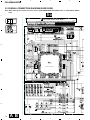
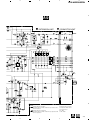
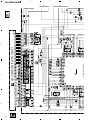
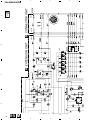
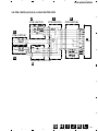
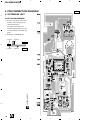
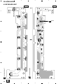
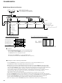
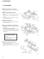
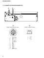
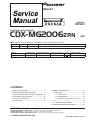
RENAULT
Service
Manual
ORDER NO.
CRT2412
6 DISC IN-DASH CD CHANGER
CDX-MG2006ZRN
EW
- This service manual should be used together with the following manual(s):
Model No.
CX-890
Order No.
CRT2376
VEHICLE
ESPACE, AVANTIME
Mech. Module
G1
DESTINATION
EUROPE
Remarks
CD Mechanism Module:Circuit Description, Mechanism Description, Disassembly
PRODUCED AFTER
April 2000
RENAULT PART No.
6025 40 2760
ID No.
PIONEER MODEL No.
CDX-MG2006ZRN/EW
CONTENTS
1.
2.
3.
4.
5.
6.
SAFETY INFORMATION ............................................2
EXPLODED VIEWS AND PARTS LIST .......................3
BLOCK DIAGRAM AND SCHEMATIC DIAGRAM ...10
PCB CONNECTION DIAGRAM ................................26
ELECTRICAL PARTS LIST ........................................42
ADJUSTMENT..........................................................46
7. GENERAL INFORMATION .......................................48
7.1 DIAGNOSIS ........................................................48
7.1.1 TEST MODE ..............................................48
7.1.2 DISASSEMBLY .........................................54
7.1.3 CONNECTOR FUNCTION DESCRIPTION .......58
7.2 IC ........................................................................59
7.3 SYSTEM BLOCK DIAGRAM ..............................61
8. OPERATIONS AND SPECIFICATIONS.....................62
PIONEER CORPORATION
4-1, Meguro 1-Chome, Meguro-ku, Tokyo 153-8654, Japan
PIONEER ELECTRONICS SERVICE INC. P.O.Box 1760, Long Beach, CA 90801-1760 U.S.A.
PIONEER EUROPE N.V. Haven 1087 Keetberglaan 1, 9120 Melsele, Belgium
PIONEER ELECTRONICS ASIACENTRE PTE.LTD. 253 Alexandra Road, #04-01, Singapore 159936
C PIONEER CORPORATION 2000
K-ZZB. FEB. 2000 Printed in Japan
CDX-MG2006ZRN
- CD Player Service Precautions
1. For pickup unit(CXX1311) handling, please refer
to"Disassembly"(see page 54).
During replacement, handling precautions shall be
taken to prevent an electrostatic discharge(protection
by a short pin).
2. During disassembly, be sure to turn the power off
since an internal IC might be destroyed when a connector is plugged or unplugged.
3. Please checking the grating after changing the service pickup unit(see page 46).
- When the Repair is Complete
When the repair is complete, make the CD mechanism
ready for transportation implementing the following
procedures:
1. Press the changer side 1 and 4 simultaneously to turn
the ACC on.
2. As the ACC is turned on, the disc indicator blinks in
red.
3. When the blinking is stopped, the mechanism is
ready for the transportation.
4. Attach the Transportation Bracket (CNC7878). Now
you can transport it.(See the figure below)
Transportation Bracket
(CNC7878)
Case
(CNB2527)
1. SAFETY INFORMATION
This service manual is intended for qualified service technicians; it is not meant for the casual do-it-yourselfer.
Qualified technicians have the necessary test equipment and tools, and have been trained to properly and safely repair
complex products such as those covered by this manual.
Improperly performed repairs can adversely affect the safety and reliability of the product and may void the warranty.
If you are not qualified to perform the repair of this product properly and safely; you should not risk trying to do so
and refer the repair to a qualified service technician.
1. Safety Precautions for those who Service this Unit.
• When checking or adjusting the emitting power of the laser diode exercise caution in order to get safe, reliable
results.
Caution:
1. During repair or tests, minimum distance of 13cm from the focus lens must be kept.
2. During repair or tests, do not view laser beam for 10 seconds or longer.
2. A “CLASS 1 LASER PRODUCT” label is affixed to the
bottom of the player.
3. The triangular label is attached to the mechanism
unit holder.
CLASS 1
LASER PRODUCT
4. Specifications of Laser Diode
Specifications of laser radiation fields to which human access is possible during service.
Wavelength
= 800 nanometers
2
CDX-MG2006ZRN
2. EXPLODED VIEWS AND PARTS LIST
2.1 PACKING
1
2
3
6
7
4
4
5
8
NOTE:
- Parts marked by “*” are generally unavailable because they are not in our Master Spare Parts List.
- Screws adjacent to ∇ mark on the product are used for disassembly.
- PACKING SECTION PARTS LIST
Mark No. Description
*
*
*
*
1
2
3
4
5
Lid
Protector
Protector
Protector
Protector
Part No.
CHW1584
CHP2235
CHP2234
CHP2237
CHP2236
Mark No. Description
*
*
6 Protector
7 Polyethylene Bag
8 Contain Box
Part No.
CHP2238
CEG1042
CHL3990
3
CDX-MG2006ZRN
2.2 EXTERIOR
4
CDX-MG2006ZRN
- EXTERIOR SECTION PARTS LIST
Mark No. Description
Part No.
Mark No. Description
Part No.
Screw
Screw
Screw
Connector
Screw
BMZ20P020FMC
BMZ26P030FMC
BMZ26P060FMC
CDE6144
IMS26P040FMC
46
47
48
49
50
Holder
Keyboard Unit
Connector(CN901)
Bracket Unit
Screw
6
7
8
9
10
Case
Side Frame
Case
Bracket
Front frame
CNB2527
CNB2528
CNB2529
CNC7878
CNC8574
51
52
53
54
55
Screw
Damper
Holder
Screw(M2x2)
11
12
13
14
15
Bracket
Insulator
Insulator
Insulator
Insulator
CNC8816
CNM5969
CNM6248
CNM6532
CNM6533
56
57
58
59
60
Holder
CNC7477
Sheet
CNM5981
Sheet
CNM6318
Spring(Front)
CBH2409
Spring(Right Rear)(Black) CBH2361
16
17
18
19
20
PCB
Clamper
Bush
Holder
Connector Unit
CNP5516
CNV5150
CNV3253
CNV5543
CWM6823
61 Spring(Left Rear)
62 Transistor(Q708)
21
22
23
24
25
Plug(CN705)
Connector(CN704)
Connector(CN703)
Holder
Extension Unit
CKS2372
CKS3180
CKS4120
CNC8575
CWM6824
26
27
28
29
30
Connector(CN777)
Connector(CN701)
Connector(CN101)
Holder
Chassis Unit
CKS3747
CKS3747
CKS3989
CNC8031
CXB4792
31
32
33
34
35
Screw
Button(1-6)
Button(EJECT)
Door
Washer
BPZ20P080FMC
CAC6344
CAC6345
CAT2185
CBF1038
36
37
38
39
40
Spring
Spring
Connector
Insulator
Insulator
CBH2200
CBH2201
CDE6143
CNM5331
CNM6818
41
42
43
44
45
Grille
Gear
Arm
Lighting Conductor
Lighting Conductor
CNS6101
CNV5547
CNV5548
CNV6028
CNV6029
1
2
3
4
5
CNV6030
CWM6822
CKS3748
CXB3111
IMS20P040FMC
CD Mechanism Module(G1) CXK4700
IMS20P040FMC
CNV5120
CNC7826
CBA1250
CBH2365
2SB1335A
5
CDX-MG2006ZRN
2.3 CD MECHANISM
6
CDX-MG2006ZRN
- CD MECHANISM SECTION PARTS LIST
Mark No. Description
•••••
CD Core Unit(Servo Unit)
Connector(CN101)
Connector(CN301)
Connector(CN201)
CWX2202
CKS2764
CKS3966
CKS3991
14
15
16
17
18
CD Core Unit(STS Unit)
Connector(CN701)
Connector(CN801)
Connector(CN802)
Screw
19
20
21
22
23
Mark No. Description
Part No.
54
55
56
57
58
Shaft
Steer
Steer
Cam
Holder
CLA3693
CNC7215
CNC7216
CNC8774
CNC7235
CWX2203
CKS3989
CKS3989
CKS4054
CBA1037
59
60
61
62
63
Gear
Gear
Lever
Lever
Lever
CNC7236
CNC8883
CNC7243
CNC7244
CNC7245
Screw
Screw
Screw
Washer
Screw
CBA1041
CBA1076
CBA1250
CBA1512
CBA1452
64
65
66
67
68
Lever
Cover
Holder Unit
Lever
Gear
CNC7246
CNC7441
CXB4946
CNC8024
CNC8140
24
25
26
27
28
Screw
Screw
Washer
Washer
Washer
CBA1453
CBA1479
CBF1037
CBF1038
CBF1039
69
70
71
72
73
Sheet
PCB
PCB
Gear
Gear
CNM5831
CNP5680
CNP5681
CNR1479
CNR1481
29
30
31
32
33
Washer
Spring
Spring
Spring
Spring
CBF1064
CBH2007
CBH2271
CBH2274
CBH2014
74
75
76
77
78
Gear
Gear
Gear
Gear
Gear
CNR1495
CNR1501
CNR1502
CNR1540
CNR1541
34
35
36
37
38
Spring
Spring
Spring
Spring
Spring
CBH2015
CBH2016
CBH2017
CBH2290
CBH2366
79
80
81
82
83
Belt
Worm Gear
Gear
Gear
Gear
CNT1080
CNV5046
CNV5047
CNV5048
CNV5049
39
40
41
42
43
Spring
Spring
Spring
Spring
Spring
CBH2064
CBH2195
CBH2196
CBH2224
CBH2250
84
85
86
87
88
Holder
Pulley
Arm
Spacer
Arm
CNV5056
CNV5058
CNV5061
CNV5066
CNV5189
44
45
46
47
48
Screw
Roller
Roller
Roller
Roller
CBA1082
CLA3154
CLA3157
CLA3159
CLA3160
89
90
91
92
93
Cover
Cover
Cover
Lever
Arm
CNV5207
CNV5424
CNV5425
CNV5427
CNV5491
49
50
51
52
53
Shaft
Spacer
Roller
Bush
Shaft
CLA3179
CLA3194
CLA3248
CLA3353
CLA3469
94
95
96
97
98
Gear
Holder
Composite PCB
Composite PCB
Chassis Unit
CNV5519
CNV5648
CNX3141
CNX2989
CXB4314
1-9
10
11
12
13
*
Part No.
*
7
CDX-MG2006ZRN
Mark No. Description
*
*
8
Part No.
Mark No. Description
Part No.
99
100
101
102
103
Frame Unit
Lever Unit
Arm Unit
Lever Unit
Lever Unit
CXB5806
CXB6026
CXB2704
CXB2708
CXB2709
144
145
146
147
148
Screw
Washer
Arm Unit
Arm Unit
Tray Assy
JFZ14P020FZK
YE15FUC
CXB5018
CXB5019
CXB4307
104
105
106
107
108
Lever Unit
Arm Unit
Lever Unit
Lever Unit
Carriage Mechanism Unit(G1)
CXB2711
CXB2712
CXB6027
CXB2714
CXB2998
149
150
151
152
153
Spring
Sheet
Cam Motor Assy
Spacer
Bracket Unit
CBH2269
CNM6699
CXB3170
CNC8289
CXB4165
109
110
111
112
113
Screw
Screw
Screw
Screw
Washer
CBA1041
CBA1250
CBA1362
CBA1471
CBF1038
154
155
156
157
158
Motor Unit(M1 Cam Gear)
CXB3174
CXB3175
JFZ20P025FMC
CXB3171
CXX1415
114
115
116
117
118
Spring
Spring
Spring
Spring
Roller
CBH2008
CBH2009
CBH2010
CBL1335
CLA3707
159
160
161
162
163
Screw
Washer
Load Arm R Assy(Service)
Washer
Spring
CBA1453
CBF1038
CXX1416
CBF1074
CBH2136
119
120
121
122
123
Bracket
Guide Unit
Cover
Sheet
Sheet
CNC7228
CXB4417
CNC7628
CNM6414
CNM5378
164
165
166
167
168
Arm
Arm
Holder
Belt
Holder
CNC7241
CXB4449
CBL1465
CNT1079
CNV5055
124
125
126
127
128
Sheet
Sheet
PCB
Ball
Bearing
CNM5695
CNM5827
CNP4978
CNR1189
CNR1423
169
170
171
172
173
Pulley
Roller
Guide
Bracket Unit
Roller Gear Unit
CNV5057
CNV6209
CNV5125
CXB4316
CXB3176
129
130
131
132
133
Belt
Holder
Guide
Clamper
Rack
CNT1079
CNV5037
CNV5040
CNV5042
CNV5111
174
175
176
177
178
Motor Unit(M2 LOAD)
Screw
Loading Arm R Assy
Screw
Washer
CXB3177
JFZ14P020FMC
CXB3172
CBA1453
CBF1074
134
135
136
137
138
Arm
Holder
Chassis
Arm Unit
CNV5579
CNV5759
CXB6025
CXB2705
Motor Unit(M4 CARRIAGE) CXB3178
179
180
181
182
183
Spring
Arm
Arm
Screw
Roller
CBH2136
CNC7242
CXB4448
JFZ20P014FMC
CNV6209
139
140
141
142
143
Screw Unit
Lever Unit
Insulator
Spacer
Motor(M5 SPINDLE)
184
185
186
187
188
Roller Gear Unit
Guide
Switch(S885 MAX)
LED(D883)
Photo-transistor(Q881)
CXB3176
CNV5126
CSN1052
CL202IRXTU
CPT231SXTD
CXB3179
CXB4450
CNM6306
CNM6345
CXM1120
*
*
*
*
*
*
*
*
*
Motor Unit(M3 ELV)
Screw
Loading Arm L Assy
Load Arm L Assy(Service)
CDX-MG2006ZRN
Mark No. Description
Part No.
189
190
191
192
193
LED(D891,892)
Switch(S887 CLAMP)
Switch(S886 ELV HOME)
Bracket Unit
CL202IRXTU
CSN1051
CSN1052
CXB4306
Photo-transistor(Q851,852) CPT231SXTD
194
195
196
197
198
Resistor(R856)
Resistor(R857)
Photo-interrupter(Q1)
Screw
Pickup Unit(Service)(P8)
RS1/8S911J
RS1/8S821J
RPI-221
CBA1387
CXX1311
9
2
1
3
4
CDX-MG2006ZRN
3. BLOCK DIAGRAM AND SCHEMATIC DIAGRAM
3.1 BLOCK DIAGRAM
C CD CORE UNIT(SERVO UNIT)
PICKUP UNIT(SERVICE)(P8)
D CD CORE UNIT(STS UN
CN101
5
LD-
RF AMP
V5
16
17
15
PD
CN201
IC101
UPC2572GS
Q101
35
69
HOLOGRAM
UNIT
MD/SD/TD/FD
3
CD 4CH DRIVER
BCL
EC
VM
VCC
8
5
6
ST/SR
B
15
IC301
BA5986FM
VR2
M
SPINDLE
MOTOR
16
22
74
BVD
V5
CONT
HOME
19
28
29
28
29
30
30
VM
5V
10
11
HOME
SWITCH
19
X201
7
GND
4M DRAM
11
10
39
IC502
MSM514400DP-60TS
MUTE
9
XTLI
A
5
IC501
CXD2511R
µ-COMPUTER
INTERFACE
11
1
2
3
4
WDCK
RFCK
RAOV
LRCK
SCKO
DOUT
MCK
DIGITAL SIGNAL
PROCESSOR
14
CARRIAGE
MOTOR
BCK
DATA
LRCK
SHOCKPROOF
CONTROL
DIGITAL SERVO
PROCESSOR
4
TO+
TRACKING ACT
8fs
EFM
Q102
FO+
FOCUS ACT
CN801
IC201
UPD63702AGF
LD
WDSL/CHMO/CHMI
LD
MD
14
XTAL
LD+
XTAL
MD
A
VD
5V
5V REGULATOR
4
V+5V
VD
IC701
BA05SFP
CN301
2
1
E MOTOR PCB(B)
F MOTOR PCB(A)
XAO/XSTB/XSO/XSI/XSCK/XRST/SCO
45
ELVSNS
PVD
44
46
ELEVATION
SENSE
S8
S8
S8
MOTOR DRIVER
CAMGEAR
MOTOR
M
G PCB UNIT(D) K LOAD MOTOR PCB
Q851
1
PH1
1
LOADING
MOTOR
C
3
5
1
6
1
J PCB UNIT(C)
PH2
Q881
S883
4
4
1
2
1
2
IC802
LB1836M
2
6
MOTOR DRIVER
EL+
3
2
5
6
IC801
LB1836M
13
9
10
PH1
2
1
D883
M
I PCB UNIT(E) H PCB UNIT(B)
1
PVD
5
12
L PCB UNIT(A)
D891 D892
CG+
3
2
M
3
EL-
ELEVATION
MOTOR
Q852
CG-
PVD
3
PH1
4
PH2 2
MAXSW
1
LD MOTOR-
5
7
7
5
PVD
PH1
3
4
9
8
PH2
2
10
5
6
LD MOTOR+
3
4
2
MAXSW
ELV HOME
S886
1
S887
CLAMP
1
11
10
2
11
1
LOLO+
Q801
PVD
VD
PVD
LOAD
Q802
ELHOME
CLAMP
CN802
B KEYBOAR
MAX
SWITCH
RAMP
D905~91
D
LED
IC901
KEY MATRIX
10
1
2
3
4
5
7
6
8
CDX-MG2006ZRN
A EXTENSION UNIT
TS UNIT)
M CONNECTOR UNIT
CN703
CN777
8fs DF D/A LPF
IC601
AK4321VF
5
12
LCH
6
42
2
9
LCH
PD
ISOLATOR
LPF
CN101
CN701
18
IC101
NJM4558MD
CN704
IC102
BA3121F
3
1
1
Q101
5.0V REGULATOR
Q704
14
14
15
RCH
16
SRQ 6
15
16
6
LCH
D101
DEMO
B.U
MUTE
VDD
RST
Q102
RXEN
WDSL/CHMO/CHMI
XWRE/XRDE/XQOK
XWIH/XEMP/ADRMON/CHDT
VDD
SCK
Q103
P-BUS
DATA
8.8V REGULATOR
Q708
VD
VD
8
43
9
42
Q709
B.U
11
11
12
12
10
10
7
7
1
1
2
2
3
3
4
4
B.UP
16
12
B.UP
B.UP SENSE
B.UP
Q702
WDSL/CHMO/CHMI
XWRE/XRDE/XQOK
XWIH/XEMP/ADRMON
CHDT
B.UP
4
ELV2
5
LO1
2
LO2
3
MAXSW 47
PH2 46
PH1
45
60
47
59
44
CLAMP 43
12 SCK
13 DATA
3 B. UP
B
XOUT
XIN
BSO
BSENS
BSCK
BRST
BRXEN
29
SYSTEM
CONTROLLER
2
1
ELV1
IC601
LO1
57 LO2
78 MAXSW
77
PH2
76 PH1
PD5553A
3
58
49
48
4
5
6
6
ELHOME
CG1
CG2
ELV2
46
55
LOAD 12
9
V+5V
VD
OAD
5
13
5
39
C
LOAD
ELHOME
CLAMPSW
40 14
7
70 68 66 67
25
8
RESET
2
IC701
EXMODE
40
6
MODESW
EXSO
11
61
1
7
LOADSW
EXSCK
44
2
8
12 11 10
1
CLK
45
62
11 RXEN
3
DOORSW
ILPOW
6
ELV1
4
3
7
CG2
V+5V
1
2
10 RST
E
4
ELVSNS
DATA
CG1
3
2
28
20 22
RESET
S802
S803
79
50
EJKEY
1
LOADSW
50
DOORSW
49
MODESW
48
S801
DCLOSE
ELVSNS
BSRQ
XRST/SCONT
17 16 18 19
56
CDMUTE
POWER
CONT
26
VDCONT
53 27 13
41
AUDIO GND
R CH
SRQ
X601
EMPH
POWER 10
L CH
CN705
Q710
VD
2
1
3
4
9
VDD
Q711
CONT
35
EMPH
39
A
VDD
BOARD UNIT
S-80740AND4I
DOORSW
3 DOORSW
ILPOW2
3
ILPOW2 15
15
16
16
ILPOW
Q705
D750
ILPOW
8.2V REGULATOR
Q777
Q750
Q706
D905~916
EJECT
20
VDD 2
LED DRIVER
IC901
BU2092FV
9
9
1
1
4
VDD
8
6 DATA
8 CLK
7
7 MODE
6
3
EJECT
B.U
ILL
D601
5
6
Q751
3
2 1
4
D
ILL
Q707
5
5
2 ILL
KEY DATA
CN901
CN701
11
5
6
7
8
2
1
3
4
CDX-MG2006ZRN
3.2 OVERALL CONNECTION DIAGRAM(GUIDE PAGE)
Note: When ordering service parts, be sure to refer to “EXPLODED VIEWS AND PARTS LIST” or “ELECTRICAL PARTS
LIST”.
A-a
A
A-a
A-a
A-a
A-b
A-b
A-b
D CD CORE UNIT(STS UNIT)
Large size
SCH diagram
CN701
CN101
Guide page
Detailed page
B
SYSTEM CONTROLLER
C
CN901
CN701
D
B KEYBOARD UNIT
12
A B
1
2
3
4
5
7
6
8
CDX-MG2006ZRN
A
A-b
A EXTENSION UNIT
M CONNECTOR UNIT
CN704
CN703
CN777
B
E
2
1
6
5
12 11 10
9
4
3
8
7
13
P-BUS
C
CN705
1
2
3
D
NOTE :
Symbol indicates a resistor.
No differentiation is made between chip resistors and
discrete resistors.
Symbol indicates a capacitor.
No differentiation is made between chip capacitors and
discrete capacitors.
5
6
Decimal points for resistor
and capacitor fixed values
are expressed as :
2.2 ← 2R2
0.022 ← R022
7
AM
8
13
C
14
1
CN101
CN701
2
2
2
1
1
SYSTEM CONTROLLER
D CD CORE UNIT(STS UNIT)
A
A-a A-b
CDX-MG2006ZRN
3
3
4
B
D
A-a
4
B KEYBOARD UNIT
SYSTEM CONTROLLER
CN901
CN701
A-a A-b
3
5
5
6
6
7
CDX-MG2006ZRN
7
8
A-a B
8
15
A
B
C
D
16
A-b M
1
P-BUS
CN703
2
3
9
12 11 10
13
5
7
8
1
2
6
3
4
E
CN704
2
2
CN777
M CONNECTOR UNIT
1
1
B
A EXTENSION UNIT
A
A-a A-b
CDX-MG2006ZRN
3
4
C
D
4
5
3
NOTE :
Symbol indicates a resistor.
No differentiation is made between chip resistors and
discrete resistors.
Symbol indicates a capacitor.
No differentiation is made between chip capacitors and
discrete capacitors.
2
3
6
6
7
7
A-a A-b
Decimal points for resistor
and capacitor fixed values
are expressed as :
2.2 ← 2R2
0.022 ← R022
1
CN705
5
CDX-MG2006ZRN
8
A-b M
8
17
A
B
C
D
2
1
3
4
CDX-MG2006ZRN
3.3 CD CORE UNIT(SERVO UNIT)
A
D CD CORE UNIT(SERVO UNIT)
C
RF AMP/
AUTO POWER
CONTROL
(SERVICE)(P8)
B
2.5V
C
CD DRIVER
E
MOTOR PCB(B)
M4 CARRIAGE
CXB3178
DISC INSERT DETECT
D
M5 SPINDLE
CXM1120
18
C E
1
2
3
4
5
7
6
8
CDX-MG2006ZRN
A
B
FOCUS/TRACKING
CARRIAGE/SPINDLE
DIGITAL SERVO
DIGITAL SIGNAL PROCESSOR
D/A CONVERTER
16.934MHz
C
22/6R3
F
5
6
D
7
C
8
19
2
1
3
4
CDX-MG2006ZRN
3.4 CD CORE UNIT(STS UNIT)
G
D CD CORE UNIT(STS UNIT)
B
CD CORE UNIT
D (SERVO UNIT)
C
A
SURE TRACK
MEMORY CONTROL
M1 : CXB3174
ELV SENSE
Q1 : RPI-221
+5V REGULATOR
M3 : CXB3175
C
MOTOR PCB
(A)
F
7.5V
9.0V
MOTOR DRIVER
LOAD SWITCH
H
DOOR SWITCH
MODE SWITCH
D
20
D F
1
2
3
4
5
7
6
8
CDX-MG2006ZRN
A
22/6R3
D/A CONVERTER
RACK
RY CONTROLLER
B
A
CN101
4M DRAM
C
IVER
MOTOR DRIVER
D
5
6
7
D
8
21
CDX-MG2006ZRN
Note:1. The encircled numbers denote measuring pointes in the circuit diagram.
2. Reference voltage
REFOUT:2.5V
- Waveforms
1 RFO
0.5V/div. 0.2µs/div.
Normal mode: play
1 RFO
Test mode
0.5V/div. 0.5µs/div.
1 CH1: RFO
1V/div.
0.5ms/div.
2 CH2: MIRR 5V/div.
Normal mode: The defect part
passes 500µs/div.
REFOUT→
REFOUT→
REFOUT→
REFOUT→
GND →
1 CH1: RFO
1V/div. 0.5ms/div.
2 CH2: MIRR
5V/div.
Test mode: Tracking open
GND →
3 CH1: FIN
0.5V/div.
0.2s/div.
5 CH2: FOK
2V/div.
Normal mode: Focus close
3 CH1: FIN
0.5V/div.
0.2s/div.
4 CH2: FOP
2V/div.
Test mode: No disc, Focus close
REFOUT→
REFOUT→
REFOUT→
REFOUT→
GND →
6 CH1: FEY
0.5V/div.
1ms/div.
7 CH2: XSI
2V/div.
Normal mode: Focus close
8 CH1: TEY
0.5V/div. 0.5ms/div.
9 CH2: TIN
0.5V/div.
Test mode: 32 tracks jump (FWD)
8 CH1: TEY
0.5V/div. 0.5ms/div.
9 CH2: TIN
0.5V/div.
Test mode: Single jump (FWD)
REFOUT→
REFOUT→
REFOUT→
REFOUT→
REFOUT→
GND →
6 CH1: FEY
0.1V/div.
3 CH2: FIN
0.2V/div.
Normal mode: Play
REFOUT→
20ms/div.
3 CH1: FIN
0.5V/div. 0.5s/div.
0 CH2: SIN
1V/div.
Normal mode: Focus close
REFOUT→
0 SIN
Normal mode: Play
REFOUT→
REFOUT→
REFOUT→
22
REFOUT→
0.5V/div.
0.1s/div.
CDX-MG2006ZRN
8 CH1: TEY
6 CH2: FEY
0.5V/div.
0.1V/div.
0.2s/div.
8 CH1: TEY
! CH2: SD
0.5V/div.
0.5V/div.
5ms/div.
1V/div.
5V/div.
500µs/div.
Normal mode: The defect part passes 800µm
Normal mode: AGC after focus close
REFOUT→
REFOUT→
REFOUT→
REFOUT→
REFOUT→
0 SIN
3 CH1: FIN
$ CH2: HOLD
REFOUT→
GND →
1V/div.
10ms/div.
Long Search
1 CH1: RFO
$ CH2: HOLD
1V/div.
5V/div.
500µs/div.
Normal mode: The defect part passes 800µm
8 CH1: TEY
1V/div.
2ms/div.
# CH2: TEC
1V/div.
Test mode: Focus close
Tracking open
REFOUT→
REFOUT→
REFOUT→
GND →
REFOUT→
REFOUT→
6 CH1: FEY
0.2V/div.
1ms/div.
3 CH2: FIN
0.5V/div.
Normal mode: During AGC
8 CH1: TEY
0.2V/div.
1ms/div.
9 CH2: TIN
0.5V/div.
Normal mode: During AGC
@ EFM
1V/div.
2µs/div.
Play
REFOUT→
REFOUT→
REFOUT→
REFOUT→
REFOUT→
% Dout
2V/div.
5µs/div.
^ LRCK
10µs/div.
* ADRMON
1V/div.
1s/div.
Normal mode: Starting play
Play
REFOUT→
2V/div.
REFOUT→
GND →
23
CDX-MG2006ZRN
8 CH1: TEY
0.5V/div.
5ms/div.
9 CH2: TIN
0.5V/div.
Test mode: 100 tracks jump(FWD)
REFOUT→
8 CH1: TEY
0.5V/div.
9 CH2: TIN
0.5V/div.
Normal mode: Play
10ms/div.
& SCKO
Play
REFOUT→
REFOUT→
REFOUT→
) CH1: RCH
2V/div.
200µs/div.
( CH2: LCH
2V/div.
Normal mode: PLAY (0dB,1kHz)
AAGND →
AAGND →
24
REFOUT→
2V/div.
500ns/div.
1
3
2
4
CDX-MG2006ZRN
3.5 PCB UNIT(A,B,C,D,E), LOAD MOTOR PCB
PCB UNIT(C)
L
A
H
I
J
PCB UNIT(B)
PCB UNIT(E)
SWITCH
PCB UNIT(A)
D
G
CN802
B
CXB3177
PCB UNIT(D)
G
M
LOAD MOTOR PCB
K
C
D
1
2
G H I J K L
3
4
25
2
1
3
4
CDX-MG2006ZRN
4. PCB CONNECTION DIAGRAM
A
SIDE A
4.1 EXTENSION UNIT
NOTE FOR PCB DIAGRAMS
1. The parts mounted on this PCB
include all necessary parts for
several destination.
For further information for
respective destinations, be sure
to check with the schematic diagram.
2. Viewpoint of PCB diagrams
Connector
Capacitor
SIDE A
B
P.C.Board
Chip Part
SIDE B
A EXTENSION UNIT
C
D
26
A
1
2
3
4
1
2
3
4
CDX-MG2006ZRN
SIDE B
A
B CN901
B
C
A EXTENSION UNIT
D CN701
D
M CN703
1
2
3
A
4
27
2
1
3
4
CDX-MG2006ZRN
4.2 KEYBOARD UNIT
SIDE A
6
DOOR SW
A
SIDE B
5
A
3
4
B
28
B
1
2
B KEYBOARD UNIT
1
EJECT
D
B KEYBOARD UNIT
2
C
3
4
CN701
1
2
3
4
CDX-MG2006ZRN
4.3 CONNECTOR UNIT
A
M CONNECTOR UNIT
SIDE A
A
CN777
B
SIDE B
M CONNECTOR UNIT
C
D
1
2
3
M
4
29
2
1
3
4
CDX-MG2006ZRN
4.4 CD CORE UNIT(SERVO UNIT)
A
E
SIDE A
F
B
C CD CORE UNIT(SERVO UNIT)
D
PICKUP UNIT(SERVICE)(P8)
C
30
C
1
2
3
4
1
2
3
4
CDX-MG2006ZRN
SIDE B
A
B
C CD CORE UNIT(SERVO UNIT)
C
D
C
1
2
3
4
31
2
1
3
4
CDX-MG2006ZRN
4.5 CD CORE UNIT(STS UNIT)
D CD CORE UNIT(STS UNIT)
SIDE A
A CN101
A
H
B
F
C
D
32
D
1
2
3
4
1
2
3
4
CDX-MG2006ZRN
SIDE B
D CD CORE UNIT(STS UNIT)
A
B
C
D
D
1
2
3
4
33
1
2
3
4
CDX-MG2006ZRN
4.6 MOTOR PCB(B)
M5
SPINDLE MOTOR
E MOTOR PCB(B)
A
B
C
D
34
E
1
2
3
4
5
6
7
8
CDX-MG2006ZRN
12
D
C
CN301
1
A
B
C
D
M4
M
CARRIAGE
5
6
7
E
8
35
1
2
3
4
CDX-MG2006ZRN
SIDE A
4.7 MOTOR PCB(A)
Q1
A
F MOTOR PCB(A)
M3 ELV
M1 CAM GEAR
M
M
ELV SENSE
B
30
1
C
D
C
CN201
D
36
F
1
2
3
4
1
3
2
4
CDX-MG2006ZRN
SIDE B
F MOTOR PCB(A)
A
B
C
D
D
G
CN801
1
2
41
50
1
3
F
4
37
1
2
3
4
CDX-MG2006ZRN
4.9 PCB UNIT(B)
4.8 PCB UNIT(D)
I
A
G PCB UNIT(D)
7
1
S886
ELV
S887
CLAMP
H PCB UNIT(B)
B
C
D
38
GH
1
G
D
CN802
2
3
4
11
1
1
3
2
4
CDX-MG2006ZRN
4.10 PCB UNIT(E)
I
I
PCB UNIT(E)
PCB UNIT(E)
A
SIDE A
SIDE B
B
C
D
1
2
3
I
39
4
2
1
3
4
3
4
CDX-MG2006ZRN
4.11 PCB UNIT(C)
A
Q881
J PCB UNIT(C)
S885
MAX DETECT
B
D883
C
D
4
I
1
40
J
1
2
1
2
3
4
CDX-MG2006ZRN
4.12 LOAD MOTOR PCB
A
K
G
M
LOAD MOTOR PCB
II
1
4
2
1
M2
LOADING
M
B
4.13 PCB UNIT(A)
L
PCB UNIT(A)
C
D892
D891
1
2
I
D
1
2
3
K L
4
41
CDX-MG2006ZRN
5. ELECTRICAL PARTS LIST
NOTE:
- Parts whose parts numbers are omitted are subject to being not supplied.
- The part numbers shown below indicate chip components.
Chip Resistor
RS1/_S___J,RS1/__S___J
Chip Capacitor (except for CQS.....)
CKS....., CCS....., CSZS.....
=====Circuit Symbol and No.===Part Name
--- -----------------------------------------------
Number
Unit Name
A Unit
Part No.
-------------------------
: CWM6824
: Extension Unit
MISCELLANEOUS
IC
IC
IC
IC
Q
101
102
601
701
101
IC
IC
IC
IC
Transistor
NJM4558MD
BA3121F
PD5553A
S-80740AND4I
DTC343TK
Q
Q
Q
Q
Q
102
103
601
702
704
Transistor
Transistor
Transistor
Chip Transistor
Transistor
DTC343TK
2SA1586
DTA124EU
2SC2712
2SD1007
Q
Q
Q
Q
Q
705
706
707
708
709
Transistor
Transistor
Chip Transistor
Transistor
Transistor
2SD1760F5
2SA1163
2SC2712
2SB1335A
DTA124EU
Q
Q
Q
Q
Q
710
711
750
751
777
Transistor
Transistor
Transistor
Transistor
Transistor
DTC124EU
FMW1
2SA1162
IMH11A
2SD1760F5
D
D
D
D
D
101
401
402
403
404
Diode
Diode
Diode
Diode
Diode
MA142WA
MA143
MA143
MA143
MA143
D
D
D
D
D
405
601
702
703
705
Diode
Diode
Diode
Diode
Diode
MA143
MA142WK
1SR154-400
UDZS6R8(B)
UDZS5R6(B)
D
D
D
L
TH
706
707
750
701
601
Diode
Diode
Diode
Coil
Thermistor
DTZ8R2(C)
UDZS6R2(B)
PTZ3R6(A)
CTH1190
CCX1032
X
601
Radiator 6.290MHz
CSS1451
RESISTORS
R
R
R
R
R
101
102
103
104
105
RS1/16S562J
RS1/16S562J
RS1/16S682J
RS1/16S682J
RS1/16S432J
R
R
R
R
R
106
107
108
109
110
RS1/16S432J
RS1/16S102J
RS1/16S102J
RS1/16S272J
RS1/16S272J
42
=====Circuit Symbol and No.===Part Name
--- -----------------------------------------------
Part No.
-------------------------
R
R
R
R
R
111
402
403
404
405
RS1/16S103J
RA4C473J
RS1/16S104J
RA4C681J
RS1/16S681J
R
R
R
R
R
601
602
603
604
605
RS1/16S473J
RS1/16S473J
RS1/16S473J
RS1/16S102J
RA4C222J
R
R
R
R
R
609
610
611
615
616
RS1/16S222J
RS1/16S222J
RA4C561J
RS1/16S102J
RS1/16S473J
R
R
R
R
R
617
618
620
621
622
RN1/16SE1502D
RS1/16S222J
RS1/16S473J
RN1/10SE4302D
RN1/10SE1002D
R
R
R
R
R
640
642
645
646
647
RS1/16S471J
RS1/16S471J
RS1/16S471J
RS1/16S471J
RS1/16S471J
R
R
R
R
R
648
649
651
655
656
RS1/16S471J
RS1/16S222J
RA4C222J
RA4C471J
RA4C471J
R
R
R
R
R
660
661
662
663
664
RA4C471J
RS1/16S102J
RS1/16S102J
RS1/16S102J
RS1/16S102J
R
R
R
R
R
665
666
670
672
675
RS1/16S102J
RS1/16S471J
RA4C331J
RS1/16S331J
RS1/16S471J
R
R
R
R
R
680
681
682
683
684
RS1/16S154J
RS1/16S222J
RS1/16S102J
RS1/16S912J
RS1/16S102J
R
R
R
R
R
685
689
691
692
693
RS1/16S102J
RA4C104J
RS1/16S273J
RS1/16S512J
RS1/16S104J
R
R
R
R
R
696
697
698
699
701
RS1/16S104J
RS1/16S222J
RS1/16S222J
RS1/16S222J
RS1/16S104J
CDX-MG2006ZRN
=====Circuit Symbol and No.===Part Name
--- -----------------------------------------------
Part No.
-------------------------
=====Circuit Symbol and No.===Part Name
--- -----------------------------------------------
R
R
R
R
R
702
705
711
720
721
RS1/16S473J
RS1/16S473J
RS1/10S682J
RS1/4S331J
RS1/16S223J
RESISTORS
R
R
R
R
R
722
723
724
730
731
RS1/16S103J
RS1/16S223J
RS1/16S223J
RS1/10S223J
RS1/16S101J
C
R
R
R
R
R
732
733
734
735
736
RS1/4S221J
RS1/16S511J
RS1/16S681J
RS1/16S561J
RS1/16S103J
R
R
R
R
R
737
738
739
750
751
RS1/16S273J
RS1/16S473J
RS1/16S101J
RS1/10S102J
RS1/16S103J
R
R
R
777
778
779
RS1/16S104J
RS1/10S1R0J
RS1/10S1R0J
CAPACITORS
C
C
C
C
C
101
102
103
104
105
CEV100M16
CEV100M16
CKSRYB272K50
CKSRYB272K50
CCSRCH471J50
C
C
C
C
C
106
109
110
111
112
CCSRCH471J50
CKSRYB473K16
CEV4R7M25
CEV220M6R3
CEV220M6R3
C
C
C
C
C
401
402
403
404
405
CCSRCH221J50
CCSRCH221J50
CCSRCH221J50
CKSRYB103K50
CKSRYB103K50
C
C
C
C
C
601
603
605
651
701
CKSRYB104K16
CKSRYB103K50
CKSRYB103K50
CKSRYB103K50
CEAT471M16
C
C
C
C
C
703
704
705
707
708
CEAT471M16
CKSQYB224K16
CEV220M6R3
CKSRYB473K16
CEV4R7M25
C
C
C
C
C
709
710
711
712
713
CKSRYB473K16
CKSRYB473K16
CKSRYB103K50
CEV220M16
CKSRYB473K16
C
C
714
715
CEV470M6R3
CKSRYB473K16
Number
Unit Name
M Unit
: CWM6823
: Connector Unit
R
707
Part No.
-------------------------
RS1/10S103J
CAPACITORS
B
706
CKSQYB104K50
Unit Number : CWM6822
Unit Name
: Keyboard Unit
MISCELLANEOUS
IC
D
D
D
D
901
901
902
903
905
IC
Diode
Diode
Diode
LED
BU2092FV
1SS355
1SS355
1SS355
CL200PGCTU
D
D
D
D
D
906
907
908
909
910
LED
LED
LED
LED
LED
CL150DCD(AB)
CL200PGCTU
CL150DCD(AB)
CL200PGCTU
CL150DCD(AB)
D
D
D
D
D
911
912
913
914
915
LED
LED
LED
LED
LED
CL200PGCTU
CL150DCD(AB)
CL200PGCTU
CL150DCD(AB)
CL200PGCTU
D
S
S
S
S
916
901
902
903
904
LED
Switch
Switch
Switch
Switch
CL150DCD(AB)
CSG1043
CSG1043
CSG1043
CSG1043
S
S
S
S
IL
905
906
907
910
901
Switch
Switch
Switch
Spring Switch
Lamp 60mA,8V
CSG1043
CSG1043
CSG1043
CSN1033
CEL1617
IL
903
Lamp 60mA,8V
CEL1617
RESISTORS
R
R
R
R
R
901
902
903
904
910
RS1/10S561J
RS1/10S561J
RS1/10S561J
RS1/10S561J
RS1/8S431J
R
R
R
R
R
911
912
913
914
915
RS1/8S471J
RS1/8S431J
RS1/8S471J
RS1/8S431J
RS1/8S471J
R
R
R
R
R
916
917
918
919
920
RS1/8S431J
RS1/8S471J
RS1/8S431J
RS1/8S471J
RS1/8S431J
R
921
RS1/8S471J
CAPACITORS
C
901
CKSQYB104K16
MISCELLANEOUS
D
D
D
701
704
707
Diode
Diode
Diode
ERA15-02VH
1SS355
ERA15-02VH
43
CDX-MG2006ZRN
=====Circuit Symbol and No.===Part Name
--- -----------------------------------------------
C
Part No.
-------------------------
Unit Number : CWX2202
Unit Name
: CD Core Unit(Servo Unit)
MISCELLANEOUS
IC
IC
IC
Q
Q
101
201
301
101
102
IC
IC
IC
Transistor
Transistor
UPC2572GS
UPD63702AGF
BA5986FM
2SD1664
UMD2N
D
X
EF
301
201
201
Diode
Ceramic Resonator 16.934MHz
Filter
1SR154-400
CSS1457
CCG1076
RESISTORS
=====Circuit Symbol and No.===Part Name
--- -----------------------------------------------
Part No.
-------------------------
C
C
C
C
C
106
107
108
109
110
CKSRYB222K50
CEV4R7M35
CKSRYB273K25
CCSRCH101J50
CKSQYB104K16
C
C
C
C
C
111
112
113
114
115
CKSRYB332K50
CKSQYB473K16
CKSRYB103K25
CKSRYB391K50
CCSRCH121J50
C
C
C
C
C
116
117
118
119
120
CKSRYB682K50
CKSRYB333K16
CKSQYB334K16
CKSQYB334K16
CKSQYB334K16
C
C
C
C
C
121
122
123
124
125
CKSQYB334K16
CKSQYB104K16
CKSRYB472K50
CKSQYB104K16
CCSRCH5R0C50
C
C
C
C
C
126
127
201
202
203
CKSRYB153K25
CKSRYB102K50
CKSQYB334K16
CKSQYB104K16
CKSQYB104K16
C
C
C
C
C
204
207
208
209
210
CKSRYB471K50
CKSQYB683K16
CKSRYB821K50
CKSRYB273K25
CKSQYB334K16
C
C
C
C
C
211
212
213
301
302
CKSQYB334K16
CKSQYB334K16
CCH1300
CEV101M10
CEV101M10
R
R
R
R
R
101
102
104
105
106
RS1/8S100J
RS1/8S120J
RS1/16S822J
RS1/16S682J
RS1/16S183J
R
R
R
R
R
107
108
109
110
111
RS1/16S822J
RS1/16S333J
RS1/16S683J
RS1/16S134J
RS1/16S273J
R
R
R
R
R
112
113
114
115
116
RS1/16S222J
RS1/16S103J
RS1/16S103J
RS1/16S102J
RS1/16S163J
R
R
R
R
R
117
120
121
125
201
RS1/16S163J
RS1/16S101J
RS1/16S101J
RS1/16S0R0J
RS1/16S104J
R
R
R
R
R
202
203
204
205
206
RS1/16S103J
RS1/16S332J
RS1/16S752J
RS1/16S752J
RS1/16S101J
MISCELLANEOUS
R
R
R
R
R
250
251
252
253
254
RS1/16S331J
RS1/16S331J
RS1/16S331J
RS1/16S331J
RS1/16S331J
IC
IC
IC
IC
IC
501
502
601
701
801
IC
IC
IC
IC
IC
CXD2511R
R
R
R
R
R
255
256
259
263
269
RS1/16S471J
RS1/16S471J
RS1/16S221J
RS1/16S471J
RS1/16S0R0J
IC
Q
Q
D
D
802
801
802
701
702
IC
Transistor
Transistor
Diode
Diode
LB1836M
DTA123JK
UN2211
1SR154-400
1SR154-400
R
R
R
R
R
R
R
R
R
R
274
277
301
302
303
304
305
306
307
308
RS1/16S471J
RS1/16S471J
RS1/16S103J
RS1/16S153J
RS1/16S103J
RS1/16S273J
RS1/16S103J
RS1/16S752J
RS1/16S103J
RS1/16S103J
D
D
D
D
D
703
704
705
706
707
Diode
Diode
Diode
Diode
Diode
1SS355
1SS355
1SS355
1SS355
1SS355
D
S
S
S
EF
708
801
802
803
701
Diode
Spring Switch(LOAD)
Spring Switch(DOOR)
Spring Switch(MODE)
Filter
1SS355
CSN1052
CSN1052
CSN1052
CCG1051
R
R
309
311
RS1/16S471J
RS1/16S471J
EF
702
Filter
CCG1051
44
101
102
103
104
105
Number
Unit Name
D Unit
: CWX2203
: CD Core Unit(STS Unit)
MSM514400DP-60TS
AK4321VF
BA05SFP
LB1836M
RESISTORS
CAPACITORS
C
C
C
C
C
22µF/6.3V
CEV101M6R3
CKSQYB104K16
CEV470M6R3
CKSQYB334K16
CCSRCH240J50
R
R
R
R
R
501
502
503
504
505
RS1/16S102J
RS1/16S202J
RS1/16S392J
RS1/16S822J
RS1/16S163J
CDX-MG2006ZRN
=====Circuit Symbol and No.===Part Name
--- -----------------------------------------------
Part No.
-------------------------
R
R
R
R
R
506
507
508
509
510
RS1/16S512J
RS1/16S182J
RS1/16S222J
RS1/16S102J
RS1/16S102J
R
R
R
R
R
511
512
513
514
601
RS1/16S102J
RS1/16S102J
RS1/16S102J
RS1/16S471J
RS1/16S101J
R
R
R
R
R
602
603
604
701
702
RS1/16S101J
RS1/16S471J
RS1/16S471J
RS1/10S0R0J
RS1/10S100J
R
R
R
R
716
717
718
801
RS1/16S471J
RS1/16S471J
RS1/16S471J
RS1/10S102J
F
Q
M
M
E
M
M
Unit Number :
Unit Name
: Motor PCB(A)
1
1
3
Photo-interrupter
Motor Unit(Cam Gear)
Motor Unit(ELV)
Unit Number :
Unit Name
: Motor PCB(B)
4
5
Motor Unit(Carriage)
Motor(Spindle)
Number
Unit Name
K Unit
M
RPI-221
CXB3174
CXB3175
2
CXB3178
CXM1120
:
: Load Motor PCB
Motor Unit(Load)
CXB3177
Miscellaneous Parts List
Pickup Unit(Service)(P8)
CXX1311
CAPACITORS
C
C
C
C
C
501
502
503
504
506
CKSQYB334K16
CKSQYB334K16
CKSQYB334K16
CCSRCH471J50
CCSRCH221J50
C
C
C
C
C
601
602
603
604
605
CKSQYB334K16
CCSRCH221J50
CKSQYB334K16
CKSQYB334K16
CCH1300
C
C
C
C
C
606
701
702
703
704
C
C
C
801
802
803
22µF/6.3V
CKSQYB104K25
CKSQYB104K25
CEVL220M16
Number
Unit Name
G Unit
Q
Q
851
852
I
R
R
J
Q
D
S
L
D
D
:
: PCB Unit(D)
Photo-transistor
Photo-transistor
CPT231SXTD
CPT231SXTD
Unit Number :
Unit Name
: PCB Unit(E)
856
857
RS1/8S911J
RS1/8S821J
Unit Number :
Unit Name
: PCB Unit(C)
881
883
885
Photo-transistor
Chip LED
Spring Switch(MAX)
CPT231SXTD
CL202IRXTU
CSN1052
Unit Number :
Unit Name
: PCB Unit(A)
891
892
Chip LED
Chip LED
Number
Unit Name
H Unit
S
S
CKSQYB334K16
CCH1300
CEVL101M6R3
CKSQYB334K16
CKSQYB334K16
22µF/6.3V
886
887
CL202IRXTU
CL202IRXTU
:
: PCB Unit(B)
Spring Switch(ELV Home)
Spring Switch(Clamp)
CSN1052
CSN1051
45
CDX-MG2006ZRN
6. ADJUSTMENT
CHECKING THE GRATING AFTER CHANGING THE PICKUP UNIT
• Note :
The grating angle of the PU unit cannot be adjusted after the PU unit is changed. The PU unit in the CD mechanism module is adjusted on the production line to match the CD mechanism module and is thus the best adjusted
PU unit for the CD mechanism module. Changing the PU unit is thus best considered as a last resort. However, if
the PU unit must be changed, the grating should be checked using the procedure below.
• Purpose :
To check that the grating is within an acceptable range when the PU unit is changed.
• Symptoms of Mal-adjustment :
If the grating is off by a large amount symptoms such as being unable to close tracking, being unable to perform
track search operations, or taking a long time for track searching.
• Method :
• Measuring Equipment
• Measuring Points
• Disc
• Mode
• Oscilloscope, Two L.P.F.
• E, F, REFOUT
• ABEX TCD-784
• TEST MODE
CD CORE UNIT(SERVO UNIT)
L.P.F.
F
E
Xch
100kΩ
E
390pF
REFOUT
F
REFOUT
Ych
Oscilloscope
100kΩ
390pF
REFOUT
L.P.F.
• Checking Procedure
1. In test mode, load the disc and switch the 5V regulator on.
2. Using the FWD and REV buttons, move the PU unit to the innermost track.
3. Press key B to close focus, the display should read "91". Press key D to implement the tracking balance adjustment the display should now read "81". Press key B 4 times. The display will change, returning to "81" on the
fourth press.
4. As shown in the diagram above, monitor the LPF outputs using the oscilloscope and check that the phase difference is within 75° . Refer to the photographs supplied to determine the phase angle.
5. If the phase difference is determined to be greater than 75° try changing the PU unit to see if there is any
improvement. If, after trying this a number of times, the grating angle does not become less than 75° then the
mechanism should be judged to be at fault.
• Note
Because of eccentricity in the disc and a slight misalignment of the clamping center the grating waveform may be
seen to "wobble" ( the phase difference changes as the disc rotates). The angle specified above indicates the average angle.
• Hint
Reloading the disc changes the clamp position and may decrease the "wobble".
46
CDX-MG2006ZRN
Grating waveform
Ech → Xch 20mV/div, AC
Fch → Ych 20mV/div, AC
0°
30°
45°
60°
75°
90°
47
CDX-MG2006ZRN
7. GENERAL INFORMATION
7.1 DIAGNOSIS
7.1.1 TEST MODE
- CD Test Mode
1) Precautions on Adjustment
• The unit employs a single voltage (+5V) for the regulator, thus the reference potential of the signal is
RFOUT (approximately 2.5V) rather than GND.
Inadvertent contact of REFOUT and GND during
adjustment can result not only in disabling normal
potential measurement but also in exposing the pickup to strong impacts due to malfunctioning of the
servo. Therefore, you are requested to observe the
following precautions.
• Make sure that the negative probe of the measuring
instrument is not connected to RFOUT or GND.
Special care must be exercised so that the channel 1
negative probe may not be connected to the oscilloscope and the channel 2 negative probe to GND.
Since the frame of the measuring instrument is usually at the same potential as the negative probe, the
frame of the measuring instrument must be changed
to floating status.
When RFOUT is inadvertently connected to GND, you
must immediately turn off the regulator or power
supply.
• The regulator must be turned off before mounting or
dismounting filters or wiring materials.
• You should not start adjustment or measurement
immediately after the regulator is turned on. It is recommended to run the player for approximately one
minute so that it may stabilize.
• When the test mode is turned on, various protective
functions from the software become unavailable.
Thus, you must make sure that undesirable electric or
mechanical shocks are not be given to the system.
• This model employs a photo-transistor for detecting
discs at their loading or ejection. Thus, if its outer
case is removed during repair work and internal parts
are exposed to light of strong intensity, malfunctions
including the following can result:
∗ The eject button becomes inoperable during play.
Pressing the eject button does not eject a disc and
play is continued.
∗ Loading becomes unavailable.
If a malfunction is recognized, appropriate remedial
actions must be taken. Such actions include changing the light source position, changing the unit position and applying a cover to the photo-transistor.
• When you press the [EJECT] key to eject a disc, you
must not touch any other key until the ejection is
complete.
• If you press the [FWD] or [REV] for the focus search in
the test mode, you must turn the power off immediately. (Otherwise, the lens will be forced to stick to
the top or bottom, potentially resulting in the burning
of the actuator.)
48
2) Description of the Test Mode
Adjustment of this unit is done in parallel with the CD
control unit (KEH-M9100ZRN/EW), thus key operations for adjustments are done from the unit. Taking
the example of the KEH-M9100ZRN/EW, the following
describes how to turn on the test mode and operate
the keys. The keys referred to in the following are
those used on the KEH-M9100ZRN/EW.
• Turning on the Test Mode
Press the [AF] and [6] keys simultaneously to turn on
the ACC and the backup.
• Ending the Test Mode
When ACC or Back up is off, the test mode is canceled.
• Operation of TR JUMPs (except 100TR) continues
after your finger has left the key. CRG MOVE and
100TR JUMP are forced to the tracking close mode as
soon as the key is released.
• Turning the power on or off resets the JUMP MODE
to the Single TR.
CDX-MG2006ZRN
- CD Player Flowchart
[Key]
Contents
[AF]+[6]
Test Mode In
Display
[SO]
Source CD
TRACK
[BAND/REL]
Power ON
(T.OFFSET adjustment required)
[B]
Power ON
(T.OFFSET adjustment not required)
TRACK
TRACK
0
[BAND/REL]
Power Off
TRACK
99
[B]
Focus Close/S-curve/
F, EQ Measurement
*1
Focus Mode Select
TRACK
TRACK
91
[BAND/REL]
Power Off
TRACK
[BAND/REL]
Power Off
[A]
AGC/F.BIAS
*5
Display Switching
TRACK
TRACK
XX
[B]
AGC
TRACK
XX
[C]
CRG/TR Jump Count
Select
*3
TRACK
XX
TRACK
8X
8X
[FWD]
*2
CRG-/TR JumpTRACK
8X
or
[REV]
*2
CRG+/TR Jump+
TRACK
9X
CRG+
CRG-
TRACK
XX
8X
or
[REV]
[FWD]
[D]
Tracking Balance
Adjustment
TRACK
XX
XX
XX
XX
[B]
Auto Adjustment Display
/Rough Servo
*6
TRACK
TRACK
TRACK
TRACK
XX
[C]
Tracking Close
(No AGC, Applicable Servo)
[REV]
CRG+
CRG-
TRACK
XX
[A]
Tracking Close
(AGC, Applicable Servo)
[FWD]
[A]
Tracking Servo
Close
[C]
TRACK
8X
9X
or
9X
[D]
Trackig Open
TRACK
8X
9X
or
or
9X
*4
[D]
[BAND/REL]
Power Off
Trackig Open
TRACK
TRACK
8X
or
9X
*1) Switching must take place in the following sequence.
99 : Focus Close →
1 : S.Curve Check →
2 : Focus EQ Measurement.
*2) Single TR /4TR / 10TR / 32TR / 100TR
*3) Switching must take place in the following sequence.
Single TR
→ 4 TR → 10 TR → 32 TR → 100 TR → CRG Move
96(86)
95(85)
92(82)
93(83)
94(84)
9X(8X):91(81)
[BAND/REL] Power ON/OFF
[REV]
[FWD]
[A]
*4) It applies to the CRG Move and 100TR Jump alone.
*5) Switching must take place in the following sequence.
Min/Sec (or Track No.) → F.AGC Gain → F.AGC Gain → F. BIAS Setting
(AGC Gain = (Current value/Initial value) x 20)
*6) Switching must take place in the following sequence.
Operation
[Key]
[B]
[C]
[D]
CRG+/TR Jump+
(Toward outer perimeter)
CRG-/TR Jump(Toward inner perimeter)
Tracking Close/AGC gain,
F.Bias adjustment value display switching
Focus Close, S.Curve, F.EQ measurement/
Rough Servo/AGC
Focus Mode select/Tracking Close/
CRG,TR Jump Switching
Auto Tracking Balance adjustment/
Tracking Open
F.Cancel Display → T.Offset Display → T.Bal Display → Rough Servo.
(F.Bias value, F.Cancel value, T.Offset value, T.Bal value
= (Upper 8 bits of the setting (7F[H] to 80[H] + 80[H])/4
= 63[D] to 32[D] to 00[D]).
• Operation of TR JUMPs other than 100TR is continued after your finger has left the key.
CRG Move and 100TR Jump are forced to the Tracking Close Mode when the key is released.
• Powering on or off resets the Jump Mode to the Single TR (91).
• When ACC or Back up is off, the test mode is canceled.
Note: Sound is unavailable even after the tracking has been closed
(this trouble results when the IC for the STS is not controlled in the test mode).
Note: When you pressed the [FWD] or [REV] key during the Focus Search, you must turn the power off immediately
(otherwise, the lens can stick resulting in actuator damages).
49
CDX-MG2006ZRN
- CD Changer Mechanism Flowchart
AF
1. Back up ON(CD Changer <G1>).
2. Back up ON(Head Unit (KEH-M9100ZRN/EW)
or press CLEAR button or press RESET button.
6
SO
Display TRACK
A
BAND/REL
C
Display TRACK
Display TRACK
0
To New Test Mode
BAND/REL
B
Display TRACK
72
A
B
99
To CD Test Mode
FWD
REV
To CD Test Mode
C
Change of operation display
*1
*1
Focus stop
(Operation mode display)
75 :
Operation mode select
(Operation mode display)
72 : Stop
u
73 : CAM motor
u
74 : ELV motor
u
75 : LOAD motor
u
76 : CAM+LOAD motor
Operation start
Driven in FWD direction.
Operation start
Driven in REV direction.
Operation mode (72~76)
u
*2
State of CAM switch / ELV driving
(10~32)
(1~11)
*3
u
DISC sensing phototransistor and switch (00~07)
TRACK
7X
*2
Indicates CAMSW (CAM gear) status.
State of DISC sensing phototransistor and switch
SW1 (DOORSW) 02 pin : P77
SW2 (LOADSW) 03 pin : P76
PH1
: 76pin : P65
PH2
: 77pin : P64
MAXSW : 78pin : P63
SW3 (MODESW) 04 pin : P75
SW4 (CLAMPSW) 05 pin : P74
Display
10
30 31
REV
21 20 22 23 33 32
*4 *4
FWD
*3
PH1 PH2 MAXSW Display
L
L
L
00
H
L
L
01
L
H
L
02
H
H
L
03
L
L
H
04
H
L
H
05
L
H
H
06
H
H
H
07
L: Phototransistor is OPEN and switch is ON.
H: Phototransistor is CLOSE and switch is OFF.
- Precautions
*4 Before performing the elevation, make sure that the CAM SW (switch) is
set to a position between 22 and 20.
As a rule, driving of the ELV MOTOR must be started immediately after
the CAMSW indication has changed from 22 to 20.
When driving the CAM MOTOR in 31 → 30 → 10 (in REV direction),
the elevation position must be at the EJECT/LOAD position (the top position).
- Operating Procedures for Ejecting a Clamped Disc
1 Select CAM MOTOR[73] , then press the REV direction while the disc is being clamped (CAMSW state is 32).
The CAMSW status indication sequentially changes through 32→33→23→22.
2 When the disc to be ejected is not identical with the disc being clamped, select the ELV MOTOR[74] in the vicinity of where
the display changes from 22 to 20, then match the elevation to the disc to be ejected according to the following procedures:
After selecting ELV MOTOR[74], lower the elevation until the ELV position display becomes 01 (1st disc) using the REV direction.
Drive the elevation up until the display is changed to 10. This is the elevation where the second disk is situated.
The next display of 10 tells you the elevation of the 3rd disc. Repeating this operation allows you to establish an elevation
matching each disc. (When the elevation is driven from the 1st through 6th disc, the status display changes as
01→11→10→11→10→11→10→11→10→11→10.)
(When the disc to be ejected coincides with the disc being clamped, the above operations are not necessary.)
3 Select the CAM MOTOR [73] and then, using the REV direction, drive it until the display changes from 20 (or 22) to 21 and 31.
4 Select the ELV MOTOR [74], then drive the tray of the disc to be ejected up to the EJECT/LOAD position (using the FWD direction).
5 Select the CAM+LOAD MOTOR [76], then drive it in the REV direction until the display changes from 31 to 30 and 10.
The door will open immediately before the display changes to 10 and part of the disc will be pushed out.
6 When 10 is displayed, select the LOAD MOTOR [75], then drive it in REV direction until the disc is completely ejected.
50
CDX-MG2006ZRN
- New Test Mode
In the new test mode, the CD player plays as same as in the normal mode.
After setup, it displays error data such as out-of-focus, spindle unlocked, sub-code unreadable, and sound skipping
together with causes, error-occurred time and disc No.
During setup, the operation status of the CD control software (the internal RAM: CPOINT)
is displayed.
These functions and displayed data will help the efficiency in the service activities of aging test and failure analysis.
(1) Entering the new test mode
See the test mode flow chart on Page.49
(2) Key function table
Key
Test mode
Regulator Off
Regulator On
BAND
To regulator on
To regulator off
FWD
–
FWD-Kick
REV
–
REV-Kick
A
–
Tracking close
D
Tracking open
B
–
Focus close
–
–
Focus open
–
–
Jump off
C
To New test mode
Jump mode select
New test mode
In-play
Error/Protection
–
Time/Err.No. switching
FF/TR+
–
REV/TR–
Scan
–
Mode
–
–
–
–
–
–
Auto/Manual
Track No./Time switching
(3) Error Codes and causes
Code Category The Contents of errors
10
Electricity Off focus detected.
Causes
FOK remains low for 100 msec.
→ Damages/stains on disc, vibrations or failure on servo.
11
Electricity Spindle unlocked.
FOK = Low continued for 50 msec.
→ Damages/stains on disc, vibrations or failure on servo.
42
Electricity Sub-code unreadable.
Sub-code was unreadable for 50 msec.
→ Damages/stains on disc, vibrations or failure on servo.
43
Electricity Sound skipping detected. Last address memory function was activated.
→ Damages/stains on disc, vibrations or failure on servo.
Note: The error codes should be indicated in the same way as in the normal mode.
(4) Display of Operational Status (CPOINT) during Setup
Status No. Contents
Status No.
01
C.HOME INNER START
02
03
DURING CARRIAGE OUTER
04
05
DURING CARRIAGE OUTER FOR RETRY
11
12
SP KICK AND FOCUS SEARCH START
13
14
FOK=H WAIT
15
16
ROUGH AGC
17
18
TRACKING BALANCE AUTO CONTROL
19
1A
TRACKING CLOSE WAIT FAGC/CRG CLOSE JUNC
1B
1C
FOCUS AGC
1D
1E
MIRR, LOCK, SUBCODE CHECK
1F
20
SUPPORT JUNC
21
22
MIRR, LOCK, SUBCODE CHECK Part 2
31
32
CARRIAGE SHIFT
33
34
START CARRIAGE MOVE
35
36
TRACKING BRAKE ON
37
38
SPINDLE ROUGH SERVO
41
42
SINGLE JUMP
43
44
10TRACK JUMP
45
4D
32TRACK JUMP
4E
4F
32TRACK JUMP
Contents
DURING CARRIAGE INNER
CARRIAGE HOME END
START SETUP
XSI=L WAIT
FOK=H WAIT
RADIAL KICK
TRACKING CLOSE
BEFORE FOCUS AGC CONTROL
TRACKING AGC
TEST MODE WAIT
SPINDLE SPEED 1→2
TRACKING OPEN
WAIT TRACKING OPEN
CARRIAGE BRAKE
TRACKING BRAKE OFF
TRACKING KICK
4TRACK JUMP
32TRACK JUMP
32TRACK JUMP
51
CDX-MG2006ZRN
(5) Display Examples
1 During Setup (In case of 6-digit display and CPOINT=11H)
TRK No.
MINUTE
SECOND
11
11
11
(In case of 4-digit display, AUTO, and CPOINT=11H)
TRK No.
11
(In case of 4-digit display, MANU, and CPOINT= 1H)
MINUTE
SECOND
11
11
2 During Operation (TOC read, TRK search, Play, FF and REV)
The same as in the normal mode.
3 When a protection / Error occurred
A Error display (Use the BAND key to switch to (B) or (C).)
8-digit display : ERROR-XX
6-digit display : ERR-XX
: Err-XX
4-digit display : E-XX
B Track No. error-occurred (Use the BAND key to switch to (C).)
6 or more-digit display : TRACK MINUTE SECOND
10
40
05
4-digit display : TRACK
10
C Absolute time error-occurred (Use the BAND key to switch to (B).)
6 or more- digit display (the same as in the Track No. display mode)
: TRACK MINUTE SECOND
10
40
05
4-digit display, Manual:MINUTE SECOND
10
05
(6) P-BUS data format
1 During Setup
ADDRESS
NUMBER
61
09
ATATUS
MODE
NUMBER
MINUUTE
SEC
TRACK
STEP
BitDATA1
BitDATA2
STEP
BitDATA1
BitDATA2
STEP
BitDATA1
BitDATA2
BitDATA1
BitDATA2
FD
Disc No.
Value(CPOINT)
2-A Error display
ADDRESS
NUMBER
61
09
ATATUS
MODE
NUMBER
MINUUTE
SEC
FD
TRACK
FF
Disc No.
Error code
3-B Track No. display
ADDRESS
NUMBER
61
09
ATATUS
MODE
NUMBER
MINUUTE
SEC
TRACK
FD
Disc No
Time error occurred
Track No.
3-C Absolute time display
ADDRESS
NUMBER
61
09
ATATUS
MODE
NUMBER
Disc No.
52
MINUUTE
SEC
TRACK
STEP
FD
Absolute time
Track No.
CDX-MG2006ZRN
- Mechanism Test Mode
In this mode, operation tests such as elevation and tray-drawing /-pushing operation should be performed.
(1) Entering the mechanism test mode
See the test mode flow chart on page 50.
(2) Key function table
Key
Test mode
Regulator Off
Regulator On
BAND
To regulator on
To regulator off
FWD
–
FWD-Kick
REV
–
REV-Kick
A
To Mech.test mode
Tracking close
D
B
–
–
C
Mech. test mode
To regulator off
Driven in FWD direction
Driven in REV direction
Operation mode selection
72:Stop 73:CAM 74:ELV
75:LOAD 76:CAM+LOAD
–
Focus stop (75:LOAD)
–
–
Operation display change
Operation mode Display (72~76)
↓
CAM Switch Display (10~32)
↓
Tracking open
Focus close
Focus open
Jump off
Jump mode select
–
–
–
To New.test mode
Disc-sense photoswitch display (00~07)
(3) Display Examples
1) 6-digit display, 73:CAM
TRACK
73
TRACK
73
2) 4-digit display, 73:CAM
(4) P-BUS data format
1) 6-digit display, 73:CAM
ADDRESS
NUMBER
61
09
ATATUS
MODE
NUMBER
MINUUTE
SEC
TRACK
STEP
BitDATA1
BitDATA2
FD
Disc No.
Test operation display
53
CDX-MG2006ZRN
7.1.2 DISASSEMBLY
- Removing the upper case (not shown)
1. Remove the five screws, then remove the upper
case.
- Removing the Extension Unit (Fig. 1)
1. Remove the two screws B, then remove the side
frame .
2. Remove screw C, screw D and PCB from the connector.
3. Straighten the three currently bent claws, then
remove the extension unit.
- Removing the Grille (Fig. 1)
Fig. 1
1. Remove the two screws A and the connector,
then remove the grille.
- Removing the CD Mechanism Module (Fig. 2)
1. Remove the three screws A, then remove the
front frame.
2. Remove the three screws B and two screws C,
then remove the damper and holder.
3. Remove the two spring As, spring B and spring
C from the hook, then remove the CD mechanism module.
– Precautions on Assembly –
Fig. 2
Apply spring C (black) to the front
side hook.
Remaining springs A and B are to be
hung on the center hook.
- Removing the Keyboard Unit (Fig. 3)
holder
1. Remove the four screws B and, screw A then
remove the keyboard Unit.
2. Remove the four screws C, then remove the holder.
Grille
Fig. 3
54
CDX-MG2006ZRN
- How to remove the Tray Assy
3. Lift up the Tray assy to remove it.
* Be careful not to remove the Tray hooks from the Tray
assy.
1. Apply about 6V current to the Cam gear motor until
all holes match at the position (A) (elevation OK position).
2. Hook the three springs B temporarily as shown in Fig.
5. While pushing the Tray holder lock arms (right and
left) in the direction (C), remove the Tray holder.
ELV motor
Cam gear motor
Approximately DC 6V
Tray holder
lock arm
Tray
hooks
Tray
hooks
Tray Assy
Fig. 5
Tray holder lock arm
Tray holder
Fig.4
- How to remove the Carriage Mech. Assy
1. Insert a short pin into the flexible PCB of the Pickup
unit.
2. While opening the resin hooks, remove the cover
from the Servo unit.
3. Disconnect the flexible PCBs from the connectors
CN101 and CN301.
4. Remove the Tray holder and the Tray assy. (See
above)
5. Rotate the Cam gear motor until the positions of all
holes (E) match, then stop the motor.
(The Carriage Mech assy will stop as shown in the
Fig.7.)
Cover
Flexible
holder
Short pin
* When the positions of all holes match, they will be
completely covered by the Carriage mech assy.
* To rotate the Cam Gear motor, see "How to remove
the Tray assy".
6. Unhook the spring A.
7. Remove the flexible holder B (while opening the
hooks).
8. Remove the flexible PCB (C) from the motor. (The
flexible PCB (C) has been stuck on the motor with
double-sided adhesive tape.)
9. Loosen the fixing screw and remove the flexible
holder.
Match the hole positions
CN301
CN101
Fig. 6
55
CDX-MG2006ZRN
10. Remove the screw, pressure spring and collar. Lift
up the Carriage mechanism assy to remove it.
* Screw tightening torque: 2.6kgfcm
Screw
Pressure spring
Collar
Carriage mechanism Assy
Fig. 7
- How to remove the Pickup unit
Pulling spring
1. Remove the pulling spring, torsion spring and Eshaped ring. Then remove the Clamper arm.
* The spring (A) will be removed with the Clamper
arm.
E-shaped ring
Clamper arm
Torsion spring
Fig. 8
2. Slide the Clamp UP lever (B) to remove it.
3. Loosen the 2 screws. Remove the feed-screw cover
by sliding it.
4. Remove the feed-screw pressure spring (D).
5. Loosen the 2 screws. Remove the feed-screw holder
(E).
6. Remove the belt.
7. Remove the Pickup unit together with the feed screw.
* Be careful not to lose the shaft holders at the both
ends of the feed screw.
* Be careful not to damage the 2 flexible PCBs(for the
Pickup and motor) when separating them. The flexible PCBs have been stuck each other with doublesided adhesive tape.
Carriage
motor
White
Pickup
unit
Black
Belt
Feed screw
Fig. 9
56
CDX-MG2006ZRN
8. Loosen the 2 screws. Remove the plate spring and
the rack.
Grease (Yellow:
9. Pull out the feed screw from the Pickup unit.
PG-641)
Feed screw
Plate spring
Rack
Grease (White: KD-1)
Grease (Yellow:
PG-641)
Pickup
unit
Fig. 10
57
CDX-MG2006ZRN
7.1.3 CONNECTOR FUNCTION DESCRIPTION
B
A
A
B
P-BUS CONNECTOR (DIN 13pins)
POWER CONNECTOR (3pins)
E
4
3
2
1
8
7
6
5
12 11 10
9
1
2
3
13
1
2
3
4
5
6
7
8
9
10
11
12
13
E
58
AUDIO GND
Lch
AUDIO GND
Rch
Lch SHIELD
Rch SHIELD
NC
GND
SRQ
RST
RXEN
SCK
DATA
SHIELD GND
1
2
3
GND
ILL
B.UP
CDX-MG2006ZRN
7.2 IC
- Pin Functions (PD5553A)
Pin No.
1
2
3
4
5
6
7
8
9
10
11
12
13
14
15
16
17
18
19
20
21
22
23
24
25
26
27
28
29
30
31–33
34,35
36,37
38
39
40
41
42
43
44
45,46
47-49
50
51
52
53
54
55
56
57,58
59,60
61,62
63
64
65
66
Pin Name
VDIN
DOORSW
LOADSW
MODESW
CLAMPSW
ELHOME
XSCK
XSO
XSI
xstb
xrst
XA0
VDCONT
EJKEY
NC
brst
bsrq
erxen
bsck
bso
bsi
bsens
BSCY
CNV55
reset
POWER
CONT
XIN
XOUT
VSS
KST1-3
kdt!,@
NC
adena
testin
DCLOSE
WDSL
XWIH
XEMP
CHDT
CHM0,1
NC
xwre
xrde
xqok
EMPH
SCONT
LOAD
CDMUTE
LO2,1
ELV2,1
CG2,1
MIRR
LOCK
FOK
EXSCK
I/O
I
I
I
I
I
I
O
O
I
O
O
O
O
I
I
O
I/O
I/O
O
I
I
I
I
O
O
I
O
O
I
O
I
I
O
I
I
I
O
O
O
O
O
O
O
O
O
O
O
I
I
I
O
Function and Operation
VD power supply sensor input
Door open position sense input
Loading sense input
Elevation OK input
Disk clamp sense input
Elevation reset input
LSI clock output
LSI data output
LSI data input
LSI strobe output
LSI reset output
LSI data discernment control signal output
VD power supply control output
Eject key input
Not used
P-BUS reset input
P-BUS service request input
P-BUS busy input/output
P-BUS clock input/output
P-BUS data output
P-BUS data input
Back up power sense input
Signal indicating head of subcode block input
GND
Reset input
Servo / Mechanism power supply control output
Servo driver power supply control output
Crystal oscillating element connection pin
Crystal oscillating element connection pin
GND
Key strobe output
Key data input
Not used
A/D converter reference voltage output
Test program mode input
Door close sense input
Data comparison designation output
DRAM data white inhibit input
DRAM data read inhibit input
Data comparison mode monitor input
Data comparison mode output
Not used
DRAM data white enable output L:enable
DRAM data read enable output L:enable
SUB-Q OK output L:SUBQ OK
DAC EMPH output
Double speed select output
PHOT power supply control output
CD mute output
Load motor control output
ELV motor control output
CAM motor control output
Mirror detector input
Spindle lock detector input
Focus OK signal input
Shift clock output
59
CDX-MG2006ZRN
Pin No.
67
68
69
70
71
72
73
74
75
76,77
78
79
80
Pin Name
EXMODE
EXSO
EXCE
ILPOW
VCC
VREF
AVSS
ADRMON
EREF
PH1-3
MAXSW
ELVSNS
TEMP
I/O
O
O
O
O
I
I
I
I
I
I
I
I
Function and Operation
Latch clock output
Serial data output
Chip enable output
Illumination indicator control output
VDD
A/D converter reference voltage input
A/D converter GND
DRAM memory remaining monitor input
DRAM A/D converter reference voltage input
Disc photo sense input
Maxi CD discernment sense input
ELV position sense input
Temperature detector input
*PD5553A
80
61
1
60
20
41
21
60
40
IC's marked by* are MOS type.
Be careful in handling them because they are very
liable to be damaged by electrostatic induction.
CDX-MG2006ZRN
7.3 SYSTEM BLOCK DIAGRAM
SPEAKER
ANTENNA
-
6CD CHANGER
-
or
SYSTEM CONTROL
UNIT
-
1DIN 6CD CHANGER
(CDX-MG2006ZRN/EW)
-
CASSETTE PLAYER
REMOTE CONTROL
UNIT
(CD-R2056ZRN/X1B/WL)
DISPLAY
STEERING
REMOTE CONTROL
61
CDX-MG2006ZRN
8. OPERATIONS AND SPECIFICATIONS
8.1 OPERATIONS
Key Finder
CD Loading Slot
EJECT button
Button
CD indicators
8.2 SPECIFICATIONS
General
Power source ................... 14.4 V DC (10.5 – 16.0 V allowable)
Grounding system ............................................... Negative type
Standby current ................................................................ 2 mA
Dimensions (chassis size) .... 177.8 (W) × 50 (H) × 160 (D) mm
Weight ........................................................................... 1.55 kg
CD player
System .......................................... Compact disc audio system
Usable discs ........................................................ Compact disc
Signal format ............................. Sampling frequency: 44.1 kHz
.........................................Number of quantization bits: 16;linear
Frequency characteristics ................................. 20 – 20,000 Hz
Signal-to-noise ratio ................... 92 dB (1kHz) (IHF-A network)
Dynamic range ..................................................... 92 dB (1kHz)
Number of channels ................................................... 2 (stereo)