1
US006989659B2
(12) United States Patent
Menegoli et al.
(54)
(10) Patent N0.:
US 6,989,659 B2
(45) Date of Patent:
Jan. 24, 2006
LOW DROPOUT VOLTAGE REGULATOR
6,373,233 B2
4/2002 Bakker et al.
USING A DEPLETION PASS TRANSISTOR
6,380,769 B1 *
4/2002 Hall et al. ................ .. 327/112
6,498,367 B1 * 12/2002 Chang et al.
(75)
6,522,111 132*
2/2003 Zadeh er al. .............. .. 323/277
Car] K- Sawte“, San Jose, CA (Us)
6,586,916 B2 *
7/2003 Kalpalqian et al. ....... .. 323/268
_
_
OTHER PUBLICATIONS
(73) Ass1gnee: Acutechnology Semiconductor, San
Jose, CA (Us)
(*)
257/341
Inventors: Paolo Menegoli, San Jose, CAGE);
Notice;
Michaell R. 5Lindeburg, “Engineer-In-Training Reference
Subject to any disclaimer, the term of this
patent is extended or adjusted under 35
U.S.C. 154(b) by 0 days.
Manua ”, p. 1-13.*
Robert J. Widlar “New Developments in IC Voltage Regula
tors” IEEE Journal of Soild State Circuits, vol. 6, No. 1, Feb.
1971.
Operating and Service Manual for Model 712B PoWer
(21) Appl. No.: 10/427,384
Supply, HeWlett Packard Cornpany, Palo Alto CA, 1954, no
month.
(22) Filed:
May 2, 2003
W. Jung “LoW-Dropout Regulators”, Analog Devices, no
date.
(65)
Prior Publication Data
US 2004/0046532 A1
Mar. 11, 2004
Related US. Application Data
_ _
_
_
Burr-BroWn REG101 Speci?cation, Texas Instruments, Jul.
2001
Philips SA57000-XX speci?cations, Philips Serniconduc
t0r5> 061- 2001
W. Jung “LoW-Dropout Regulators”, Analog Devices, no
(60) Provisional application No. 60/409,040, ?led on Sep.
9, 2002.
data
* cited by examiner
51
I t. C].
( ) (£1051; 1/56
(200601)
(52)
US. Cl. ....... ......
323/274; 323/275; 323/316
(58)
Field of Classi?cation Search .............. .. 323/270,
323/273—275, 311—316
See application ?le for complete search history.
Primary Examiner—Gary L LaXton
(57)
ABSTRACT
A linear loW dropout voltage regulator is described that
makes use of a depletion rnode NMOS pass transistor and of
a PMOS transistor in series to the NMOS transistor and
(56)
References Cited
U S PATENT DOCUMENTS
' '
4,590,396 A * 5/1986 Koike ....................... .. 326/24
5,168,175 A * 12/1992 Endo ........................ .. 327/430
connected to its drain. The depletion NMOS transistor
assures loW dropout operations, While the series PMOS
transistor alloWs the current regulation even under the
Condition of shorted load_ The same PMOS transistor may
be used to disable the Current in the load Without generating
5’5O6’496 A
4/1996 wlathan
a negative voltage at the gate of the depletion pass transistor.
2
E1525:
This regulator is inherently stable Without the need for an
5,804,956 A *
9 1998 P 1 '
t' ................. .. 323 277
Output Capacitor in Parallel to the load'
6:005:378 A * 12/1999 13131111123; etal. ........ .. 323/313
6,300,749 B1
10/2001 Castelli
4 Claims, 9 Drawing Sheets
U.S. Patent
Jan. 24, 2006
Sheet 1 6f 9
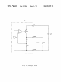
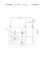
FIG. 1 (PRIOR ART)
US 6,989,659 B2
U.S. Patent
Jan. 24, 2006
Sheet 2 6f 9
US 6,989,659 B2
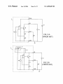
FIG. 2-A
(PRIOR ART)
CHARGE J
[ PUMP
___F
Vout
FIG 2-B
[1 RL
(PRIOR ART)
U.S. Patent
Jan. 24, 2006
Sheet 3 6f 9
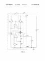
US 6,989,659 B2
5
Al
020
E[]_____ >°H1_____ {F
52
T‘
T65 22
6528
g
0
V
j
U.S. Patent
Jan. 24, 2006
Sheet 5 6f 9
US 6,989,659 B2
_
IE
ESP?
J
_“30>
_
_
lIF
_
_
_,_
E_2T
50 E26:_50
E
1
K
m
_
_
_
Qzo.|_
_
.GIm
up_|_
F_>__6:50
__z
m m=oo>
__IIl|.P
U.S. Patent
Jan. 24, 2006
$116666 6 6f 9
FIG. 6
US 6,989,659 B2
U.S. Patent
Jan. 24, 2006
US 6,989,659 B2
Sheet 7 0f 9
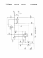
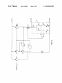
Evin
ENABLE
|:|—9| MP4
MP2 ’6__*_£| 1o00><
MP1
7*
mi]?
-
A2+
L__
MD1
lg"
A1
+
I
+——|:Jvout
UR1
(+>V2
4
FIG. 7
[1R2
I
{JGND
U.S. Patent
U
E>
Jan. 24, 2006
Sheet 8 0f 9
US 6,989,659 B2
U620
U.S. Patent
Jan. 24, 2006
Sheet 9 6f 9
US 6,989,659 B2
z
T
FI
US 6,989,659 B2
1
2
LOW DROPOUT VOLTAGE REGULATOR
USING A DEPLETION PASS TRANSISTOR
This control signal requirement limits the “dropout voltage”,
the difference betWeen the input and output voltage of the
RELATED APPLICATION DATA
regulator. In order to remove this limitation, a class of
devices referred to as “LDO” or LoW DropOut regulators
Was developed Which used common emitter or common
The present application claims priority from US. Provi
sional Patent Application No. 60/409,040 for LOW DROP
source output stages, typically PNP or PMOS transistors.
The prior art circuit 1 using the PMOS transistor is shoWn
in FIG. 1. Because the control signal (base or gate voltage)
of these devices sWings negative With respect to the emitter
OUT VOLTAGE REGULATOR USING A DEPLETION
PASS TRANSISTOR ?led on Sep. 9 2002.
10
BACKGROUND OF THE INVENTION
1. Field of the Invention
The present invention is in the ?eld of electronic circuits.
The present invention is further in the ?eld of analog
integrated circuits. The implementation is not limited to a
input voltage and it is possible to operate these devices With
eXtremely small differences betWeen input and output volt
ages.
Although the loW dropout of the standard LDO circuits is
15
either the invention as an individual component or to inclu
20
capacitor or Whether it has a series resistive component at
been common in all electronic systems. More speci?cally,
referred to as series pass regulators or loW dropout regula
tors, Which convert a higher voltage to a loWer voltage.
2. Brief Description of Related Art
Integrated circuit voltage regulators are common compo
nents Which typically have an input terminal for receiving an
input voltage, a common (ground) terminal, and an output
terminal Which supplies current to a load. The output ter
25
book “Analog Devices” in the chapter “LoW-Dropout Regu
lators” by W. Jung). As shoWn in FIG. 1 such a regulator 1
30
ampli?er. As With all feedback systems, the performance is
improved by increasing gain, but With a requirement that
35
Although many integrated circuit regulators provide this
gain be rolled off at high frequencies in order to maintain the
stability of the feedback loop. The mechanism for so limit
ing the high frequency gain is referred to as “compensation”
and is of key importance in the design of all feedback
systems.
function only, it is common to provide additional functions
in order to protect the circuitry and/or the load. It is usual to
40
regulator Will present the load. Many regulators also provide
In conventional regulator systems using unity gain fol
loWer outputs, the typical stabiliZation mechanism is to use
a three stage ampli?er. The ?rst stage is a ?Xed transcon
a means for disabling the output current, alloWing an exter
nal enable/disable signal to determine Whether the load Will
be poWered. This is typical in large electronic systems With
many individual functional blocks, Where it may be desir
able to selectively turn off those blocks to reduce poWer
includes an error ampli?er A1 having an output connected to
a gate terminal of the poWer transistor M1. A reference
voltage generator V2 is ampli?ed by a high gain feedback
the magnitude of the input voltage or the current provided to
provide a mechanism to limit the maXimum current the
too small, too much series resistance or too little) can cause
the LDO to oscillate.
The overall architecture of the series pass regulator is
typically that of a feedback ampli?er (as disclosed in the
minal provides a substantially ?Xed voltage independent of
a load, provided that the input voltage is greater in magni
tude than the desired output voltage.
the output to maintain stable operations. Many LDOs are
sensitive not only to the magnitude of capacitance across the
load, but also to Whether that capacitor looks like an ideal
high frequencies. Selecting the Wrong capacitor (too large or
energy from one DC level to another. These devices have
the invention falls into the class of voltage regulators
very desirable, this architecture has some severe limitations
in performance. The conventional regulator (using NPN or
NMOS pass transistor) typically has much loWer output
impedance. The LDO typically requires a large capacitor at
speci?c technology (i.e. CMOS or bipolar), and applies to
sion of the present invention Within larger systems Which
may be combined into a larger integrated circuit.
The invention also falls Within the ?eld of DC voltage
regulators and electronic poWer supplies, Which convert
or source terminals, this control signal is not limited by the
45
ductance, the second is a voltage gain stage, typically very
high gain, Which then drives a unity gain folloWer output
stage. Afeedback capacitor from the output or from the input
to the folloWer, or both, is connected back to the output of
consumption When they are not required. Additional protec
the transconductance stage. This feedback around causes a
tions, such as over-temperature shutdoWn, are also common.
Available regulators can be characteriZed as either shunt
dominant loW frequency pole. This architecture is identical
to the traditional feedback used in operational ampli?ers.
Because this architecture has inherently loW output
impedance, Which is further loWered by feedback, the sys
tem is relatively insensitive to loading. The reduction in
feedback With increasing frequency can make the effective
output impedance rise With frequency, causing it to look
regulators, Which place a dissipative element in parallel With
50
the load and control the shunted current to control the output
voltage, or series pass regulators, Which place a dissipative
control element directly betWeen the input voltage and the
load. The latter technique has the advantage of being sig
ni?cantly more ef?cient than the shunt variety, and is the
55
inductive. This inductive output impedance can, under cer
dominant approach used among integrated circuit regulators,
tain circumstances, interact With capacitive loading to
and is the technique used in the present invention.
Among series pass regulators, there are tWo general
reduce the stability of the system, but the systems are
generally very Wideband and load insensitive.
The standard LDO is quite different in its frequency
compensation. Typically the ampli?er has tWo or three
stages. An input stage compares a measure of the output
voltage to the voltage reference. This stage may drive
intervening stages, but eventually controls the common
source/emitter output device. That ?nal poWer stage pro
vides voltage gain as a function of its transconductance and
classes. Conventional regulators use series pass elements
Which are unity gain folloWers (emitter folloWers or source
folloWers), typically NPN or NMOS devices. This class of
60
conventional regulator, in its integrated circuit form, is Well
described in “NeW Development in IC Voltage Regulatiors”
(IEEE Journal of Solid States Circuit, vol. 6, no. 1 February
1971) by R. J. Wildlar. In order to drive the base or gate
terminals, respectively, of these devices, the controlling
signal must be higher in magnitude than the output voltage.
65
the load impedance (Av=gm*ZL). Since the load typically
includes a capacitive component, that capacitor can be used
US 6,989,659 B2
3
4
to provide some of the gain reduction at high frequencies
needed for stability. But typically the load capacitance is
Which are normally “on” and must have a negative voltage
applied to their control terminal to turn them off. One
problem is that under a condition of shorted load, Where the
output is at ground potential, the device Will be on and
cannot be turned off Without the application of a negative
controlled by system requirements other than optimizing the
stability of the LDO. It is therefore desirable to make the
LDO stable over a Wide range of capacitances.
It is not possible to use existing commercial LDOs
Without a large capacitive load (equal to or exceeding 1 uF).
This results in the control loops of most LDOs being
relatively sloW. Since the LDO has very high output imped
ance Without feedback, and a relatively loW gain at high
frequencies, it cannot maintain its output voltage in the
presence of fast load changes.
To date, the primary approach to reduce the output
capacitance sensitivity of the LDO has been to optimiZe the
frequency compensation. Miranda (US. Pat. No. 5,686,821)
gate voltage. Another potential problem With using depletion
10
mode devices is that they are uncontrolled When voltage is
initially applied. This causes the output voltage to be iden
tical to the input voltage at start-up. Only after suf?cient
voltage exists to hold the gate beloW the source (output) by
a voltage greater than the threshold voltage of the FET can
any measure of control be imposed.
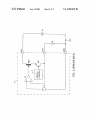
Wrathall’s solution, to both problems, shoWn in FIG. 3,
element 4, Was a regulator 4 With PMOS device M3 as a
15
and Brokaw (US. Pat. No. 5,631,598) use local capacitive
sWitch in series With the source of the depletion mode
MOSFET MD1. A sWitch control circuit 5 can selectively
feedback around the output devices and the driver stages to
turn off PMOS device M3 in order to turn off current to the
make these stages behave in a manner more similar to
load. This implementation is not the ideal con?guration,
because in the condition of very loW dropout voltage, it is
necessary to fully enhance both NMOS and PMOS devices,
i.e. maximiZing the voltage from gate to source. When the
regulated voltage is loW, the PMOS device M3 in Wrathall
cannot be fully enhanced. Similarly, by tying the source of
conventional output circuits using folloWers. Bakker et. al
(US. Pat. No. 6,373,233) provided a someWhat similar
20
solution, using a distributed RC netWork or its lumped
equivalent around the output device alone.
Castelli et. al (US. Pat. No. 6,300,749) introduced a
solution to add a mobile Zero in the compensation circuit that
is dependent on the second output pole of the LDO.
25
In all these cases the disadvantage is the need for an
output capacitor to guarantee stability and adequate ?ltering
of the output voltage.
An earlier precedent for using “normally-on” devices
comes from early regulator designs using thermionic devices
(vacuum tube triodes and beam poWer pentodes). Vacuum
There have been limited attempts to directly implement
the older, faster control scheme in LDOs. One means of
30
doing so is implemented in the UC385 regulator from
Unitrode (noW Texas Instruments). This regulator, element 2
in FIG. 2A, requires the introduction of a second higher
voltage supply voltage V3 from Which to run the control
circuit. PoWer ?oWs from the input supply V1 to the load
With very loW dropout voltage, but the gate/base drive of the
pass transistor M2 is generated from the higher voltage
35
40
unWanted noise and Would delay startup until this required
recently by Philips, the SA57000-XX.
45
mode poWer devices as pass transistors. Depletion mode
devices are those Where the turn-on threshold of the device
is of a magnitude that Zero control voltage alloWs the device
to be conducting. JFETs and vacuum tube devices are
inherently depletion mode devices, Whereas bipolar transis
50
tors are inherently enhancement mode devices, inherently
“off” With their control (base) pin held at the same potential
55
voltage spikes and to provide stability to the control loop.
SUMMARY OF THE INVENTION
60
alloWs a standard CMOS process, With one additional mask
step, to include depletion mode devices. Any process How
that builds enhancement mode MOSFETs can be modi?ed
slightly to provide depletion mode devices.
Wrathall et. al (US. Pat. No. 5,506,496) is an example of
this circuit required a sWitch SW1 that could keep the load
disconnected during start-up, as the output voltage could rise
to an uncontrolled high voltage before the active circuit
could control it.
Accordingly, What is needed is a loW dropout voltage
regulator that combines the features of inherent stability, the
ability to turn on and off very sWiftly, the possibility to
include a reliable means for limiting the output current and
PMOS devices to a desired threshold, typically a fraction of
a volt. But an additional selective implant into devices
destined to be depletion FETs can easily alter the threshold
such that it is negative, forming depletion devices. This
erence to a voltage divider taken from the output, and the
ampli?er drives a pass device U5, a beam poWer pentode.
Note that as in the LDOs formed from enhancement devices
more importantly the capability to react extremely quickly to
a change in load conditions. This Would alloW operation
Without the need for the output capacitor to ?lter the output
as the emitter. MOSFETs can be made either enhancement
or depletion by adjusting the surface concentration of the
channel region. Most production CMOS processes include
ion implantation steps to adjust the threshold of NMOS and
4, shoWs very similar architecture to the conventional solid
state series pass regulators discussed here. The gas discharge
device U8 provides a voltage reference, a feedback ampli?er
in FIG. 2, this circuit requires a multiplicity of bias voltages,
V5 and V6, in addition to the primary input voltage V4. Like
the regulator using depletion MOSFET devices as in FIG. 3,
rail is generated. Such a regulator Was introduced by Burr
BroWn (noW Texas Instruments), the REG101 and more
A more useful approach is the application of depletion
tubes, like modern depletion FETs, Were normally on With
their control terminal (grid) held at the cathode voltage. By
pulling the grid negative, the device could be turned off. A
1954 circuit for the HP 712B poWer supply, depicted in FIG.
comprising four triodes U1 through U4 compares this ref
supply. In principle, this second, higher voltage supply could
be generated by the regulator 3 using a means such as a
charge pump 4, as shoWn in FIG. 2B, but this Would create
the NMOS MD1 to the source of the PMOS M3, the Vgs
Which can be applied to the depletion NMOS is reduced
resulting in increased total on resistance or bigger die area.
65
The present invention provides a fast LDO regulator
Which is insensitive to capacitive loads. This insensitivity
alloWs the LDO to be used Without requiring a capacitive
load or, if a capacitive load is used, Without imposing
requirements on the value or quality of that capacitor. The
fact that the LDO may be used Without requiring an output
capacitor, in some applications Where it is required to turn
the use of depletion mode MOSFETs. There are several
off and on the regulator often to save energy stored in the
problems With the use of depletion mode pass devices,
batteries, such as in cellular phones, is a signi?cant advan
US 6,989,659 B2
5
6
tage because the energy stored in the output capacitor during
In normal operation, the PMOS MP1 sWitch is fully
enhanced. This placement of the PMOS device has signi?
cant advantage over prior art Wrathall. When the regulator
the on time, is then left in the capacitor at the turn off. If the
off time is long enough, due to the natural current leakage
resulting in energy Wasted at every cycle. In addition the
is being operated With substantial voltage betWeen input and
output, this con?guration provides the bene?t that the
removal of the output capacitor improves the reliability of
the overall system and reduces substantially the physical
PMOS resistance is in the drain circuit of the NMOS pass
device, rather than in series With the source. This alloWs for
siZe and the system cost.
loWer open loop output impedance, Which improves perfor
present in any capacitor, the capacitor discharges itself,
Because of its high speed, this present invention improves
signi?cantly upon the precision of the output in the presence
mance.
10
The control circuit for the PMOS MP1 additionally is
of fast transients changes in the load current. One of the
used to control fault conditions. In the case of a shorted load,
advantages of the described con?guration is the fact that the
Where the output terminal is at ground potential, it is not
possible to drive the gate of the depletion device beloW
ground to reduce the output current. Under this condition,
higher intrinsic stability and better frequency response
alloWs a potentially higher DC gain resulting in a much
better load regulation With respect to a more traditional loW 15 the PMOS can be programmed to operate at a ?Xed current
drop-out linear regulator.
Which Will control the current through the depletion NMOS
Furthermore in a con?guration Where the back gate of the
depletion transistor is tied to the substrate of the IC (most
common con?guration of CMOS processes) the intrinsic
or With a current dependent on the regulated output voltage
providing the bene?ts of current fold-back technique to limit
body diode betWeen input and output is eliminated and this
could be advantageous in some applications.
A simple implantation alloWs the addition of a depletion
addition, it is possible to turn the PMOS MP1 transistor off
to provide a “shutdown” mode Where the LDO provides no
current in the load. This shutdoWn mode may either be
contingent on a fault (such as temperature exceeding a ?Xed
the poWer in the pass transistor in case of shorted load. In
transistor to any CMOS process Without increasing the
overall cost of the regulator.
The most general embodiment for the loW dropout voltage
regulator using the depletion type ?eld effect transistor as
25
main pass element is shoWn in FIG. 5.
threshold or input voltage eXceeding a threshold) or it may
be used to provide a system-level control of poWer to the
load.
In a preferred embodiment of the present invention as
The linear regulator 6 comprises a voltage control circuit
shoWn in FIG. 7, the operational ampli?er A2 drives the gate
7 to control the voltage at the gate of the transistor MD1 in
order to regulate the voltage at the load.
of the PMOS transistor MP3, Which in its turn controls the
voltage at the gate of the PMOS transistors MP1 and MP2.
In further embodiment of the present invention as shoWn
Furthermore a current control circuit 8 controls the volt
age applied to the gate of PMOS device MP1 in order to
in FIG. 8, the error ampli?er and the reference voltage
control the current to the load.
generator are combined in the classical Bandgap circuit 10
According to the embodiment of the present invention,
the depletion pass transistor MD1 is con?gured as a folloWer
to alloW the gate voltage to regulate the voltage at its source.
comprising transistors Q1, Q2, Q3 and Q4.
35
Its back gate could be shorted to the source, but in a more
common embodiment is connected to the substrate of the
device.
The PMOS MP1 connected in series to the drain of MD1
alloWs for a complete shutdoWn of the regulator that other
Wise Would not be possible due to the negative threshold
40
A further embodiment of the present invention shoWn in
FIG. 9 presents a different type of voltage reference for use
With CMOS process technologies. In addition an operational
ampli?erA3 acts as a voltage shifter to generate a replica of
the voltage at the drain of MP3 to the gate of the transistors
MP1 and MP2.
BRIEF DESCRIPTION OF THE DRAWINGS
voltage of MD1. Furthermore MP1 could be regulated
linearly to control accurately the current in the load provid
Further details of the present invention are explained With
ing a current limit function. This current limit could be a 45 the help of the attached draWings in Which:
?Xed one or could also be made a function of the output
FIG. 1 is a circuit diagram shoWing the prior art of PMOS
voltage as used in techniques referred to as “fold-back”
LoW DropOut voltage regulator;
current control.
FIG. 2A is a circuit diagram shoWing a prior art NMOS
LDO regulator implemented With the use of an eXternal
higher voltage source generator to drive the gate of the pass
According to the general embodiment of the present
invention as shoWn in FIG. 6, a loW dropout regulator With
an input terminal Vin and output terminal Vout is provided
consisting of a voltage reference V2, a differential error
ampli?er A1 comparing said reference to a measure of the
output voltage, and a depletion mode FET MD1 Which has
its gate driven by the error ampli?er output and its source
tied to the Vout terminal. The drain of the depletion mode
transistor;
55
FET MD1 is connected to the drain of a PMOS MP1. The
PMOS transistor has its source connected to the input
terminal Vin and its gate tied to a control generator of
function to be described, Which under normal operation
holds the PMOS sWitch in an “on” state.
In typical operation, the present invention operates simi
larly to the regulators described above of conventional
design, but With the loW dropout capability of an LDO. The
use of a depletion mode device as a pass element removes 65
the requirement of an input voltage Which is substantially
greater than the desired output voltage.
FIG. 2B is a circuit diagram shoWing a prior art NMOS
LDO regulator implemented With a charge pump circuit to
generate a voltage drive for the gate of the pass transistor;
FIG. 3 is a circuit diagram shoWing a prior art depletion
NMOS LDO regulator implemented With a PMOS sWitch in
series to the source of the NMOS as in Wrathall’s patent
description;
FIG. 4 is a circuit diagram shoWing a prior art regulator
implemented With thermionic devices;
FIG. 5 is a general circuit diagram shoWing a NMOS
depletion LDO regulator circuit in accordance With the
present invention;
FIG. 6 is a circuit diagram shoWing a NMOS depletion
LDO regulator circuit in accordance With the present inven
tion;
US 6,989,659 B2
7
8
FIG. 7 is a circuit diagram showing a NMOS depletion
LDO regulator circuit in accordance With the present inven
With temperature. Similarly, the reference voltage could be
programmed, as With the output of a digital-to-analog con
tion;
verter, to make the regulator 6 programmable in output
voltage.
FIG. 8 is a circuit diagram shoWing a NMOS depletion
LDO regulator circuit combining the error simpli?er and
voltage reference functions in accordance With the present
invention; and
FIG. 9 is a circuit diagram shoWing a NMOS depletion
LDO regulator circuit combining the voltage divider and
voltage reference functions in accordance With the present
The regulation is achieved by the operational ampli?er A1
controlling the gate of MD1 in order to maintain the voltage
at its tWo inputs at the same value. Therefore the output
voltage Will be regulated at the reference voltage multiplied
10
by the resistor divider ratio.
The depletion NMOS transistor MD1 alloWs for a very
invention.
loW dropout voltage (difference betWeen the input voltage
and the output voltage) since its threshold is negative. With
DETAILED DESCRIPTION OF SPECIFIC
EMBODIMENTS
15
A. FIG. 5
FIG. 5 shoWs the most general embodiment for the loW
and source.
dropout voltage regulator 6 using the depletion MOS tran
sistor MP1 as main pass element.
The linear regulator 6 comprises a voltage control circuit
20
transistors MP2 and MP1, together With the ampli?er A2,
form a current mirror With a gain determined by their
Furthermore a current control circuit 8 controls the volt
channel Width ratio, the channel length being preferably the
age applied to the gate of PMOS device MP1 in order to
25
According to the embodiment of the present invention,
the depletion pass transistor MD1 is con?gured as a folloWer
to alloW the gate voltage to regulate the voltage at its source.
Its back gate could be shorted to the source, but in a more
common embodiment is connected to the substrate of the
Furthermore a large PMOS transistor MP1 is connected in
series to the transistor MD1. Its gate is then connected to
current control circuit 8 comprising a smaller PMOS MP2,
current loop ampli?er A2 and reference current I1. The
7 to control the voltage at the gate of the transistor MD1 in
order to regulate the voltage at the load.
control the current to the load.
no substantive voltage betWeen gate and source, as When V1
and Vout are at comparable levels, the NMOS MD1 Will be
turned fully on With a loW resistance channel betWeen drain
same for both devices. The ratio of physical siZe is made
preferably large, 1000 to 1 as shoWn in FIG. 6. Ampli?er A2
Works to force the current in MP2 to equal reference current
I1 and for the voltage at the drain of MD1 and MD2 to be
equal.
30
The operational ampli?er A2 regulates the voltage at the
device. Because it is a depletion mode device, MD1 requires
drain of MD1 to be the same as the voltage at the drain of
a negative voltage at its gate relative to its source in order to
MP2. When the voltage at the drain of MD1 drops beloW the
voltage at the drain of MP2 because the output current is
be turned fully off.
approaching the current limit threshold, the operational
The PMOS device MP1 in series With pass device MD1
alloWs the current to the load to be controlled even When the 35 ampli?er A2 raises the voltage of the gate of MP1 and MP2
to control the current in the pass transistor MD1.
gate of MD1 cannot be driven negative With respect to the
output, such as When the Vout terminal is at ground poten
The current source I1 on the drain of MP2 is set to
tial. MP1 can be controlled to be a constant current to act as
determine the output current limit as a multiple of the
a conventional current limit, or it can be made to be a
function of the output voltage or other parameters, as for
example, in a fold-back current limit that decreases the
40
channel areas of MP1 and MP2. The generation of current
sources is preferably independent of supply voltage and
temperature, and is Well knoWn in the art of analog inte
current limit value in the case of a short-circuited load.
grated circuits. The current source may also be made a
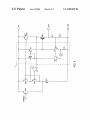
B. FIG. 6
function of input voltage, Which can provide a constant
FIG. 6 represents the general preferred embodiment for
45
the loW dropout voltage regulator using the depletion NMOS
transistor as main pass element. FIG. 6 represents a more
speci?c description of the system described in FIG. 5, With
50
connects to the non-inverting terminal of an operational
ampli?er A1, Whose output controls the gate voltage of the
main depletion pass transistor MD1 and Whose inverting
input connects to the feedback resistor divider implemented
by R1 and R2.
The reference voltage V2 is most typically generated from
a bandgap reference as is Well knoWn in the art. Other
suitable references can also be derived, for eXample from a
junction breakdoWn as With a Zener diode, or from the
difference betWeen tWo dissimilar MOSFET or JFET thresh
olds. Although this reference is generally described as a
constant voltage, this description does not preclude the use
increase the alloWable dissipation When the die is cool, or as
a function of the output voltage, to implement a fold-back
limiting function. Other functional reasons for varying the
current reference are foreseeable, and the general descrip
the current control block 8 and voltage control block 7 in
FIG. 5 replaced With practical realiZations.
The voltage control loop 7 of linear regulator 6 comprises
a voltage reference circuit V2 having an output signal that
poWer limiting, or can be made a function of temperature to
tion of this current reference as a constant current source is
not intended to limit such control of the current reference.
The regulator 6 Will operate in one of tWo modes. When
operating at a load current beloW the current limit, the output
Will be substantially controlled by the voltage control circuit
55
7. As the load current eXceeds the current limit value, the
output Will be substantially controlled by the current control
circuit 8.
When the current in the load is beloW the current limit,
both PMOS MP1 and MP2 Will be in the triode region. The
60
effective resistance of the tWo devices Will ratio as a function
of their geometry, or 1000 to 1 as shoWn. When the current
in MP1 and MD1 is substantially less than the current limit
value, the drop across MP1 Will be less than that across
MP2. This Will drive the inverting input of the ampli?er A2
of a reference Which has a functional value. For instance, a 65 more positive than the non-inverting input, causing the
reference could be generated as a function of temperature to
output of ampli?er A2 to sWing loW, further turning on both
produce an output voltage Vout for regulator 6 Which varies
MP1 and MP2 until their gate voltages are substantially at
US 6,989,659 B2
9
10
ground potential. In this mode, MP1 is effectively turned on
on further. As the current in MP2 grows to equal that of I1,
fully as a switch and MP1 plays no part in regulating the
the gate current will reduce to Zero and a stable condition
output.
will be reached.
A limitation of this current control circuitry compared to
that of FIG. 5 is that the condition that drain voltages of MP1
and MP2 being held equal is maintained over a narrower
range of voltages. As the voltage at the drain of MP1 falls
below the voltage of the common gates of MP1 and MP2,
When the current in the load increases to the value of
current limit, the ampli?er A2 actively regulates the current
in MP1 as described above. Typically, as the current limit is
reached, the output voltage will fall to a value below the
ideal regulated voltage. The voltage at the inverting input of
A1 decreases proportional to the output voltage. This drives
the output of ampli?er A1 positive and MD1 is turned fully
ampli?erA2 drives the gate of MP3 substantially to ground,
10
on. The pass device MD1 becomes a fully enhanced switch
in series with the current of the PMOS MP1 which effec
with the drain and gate of MP2 being effectively connected
together through the low impedance of switch MP3. In this
tively regulates the load.
C. FIG. 7
FIG. 7 represents the ?rst preferred embodiment for the
con?guration, the circuit continues to operate as described
15
transistor MD1 as main pass element. This embodiment
D. FIG. 8
provides a more practical current control implementation
FIG. 8 displays another embodiment of the present inven
than the general implementation of FIG. 6, and adds a logic
input that can selectively enable or disable the operation of
tion for the low dropout voltage regulator using the deple
tion NMOS MD1 transistor as main pass element. This
embodiment is similar to that of FIG. 7 but demonstrates that
the functions of the error ampli?er A1 and the reference
the regulator.
The linear regulator comprises a voltage reference circuit
V2 having an output signal that connects to the non
transistor MD1 and whose inverting input connects to the
feedback resistor divider implemented by R1 and R2. The
voltage control loop so implemented is identical to that
described above for FIG. 6.
Furthermore a large PMOS transistor MP1 is connected in
series to the transistor MD1. Its gate is then connected to the
gate of the PMOS transistor MP2 of the same type, but
smaller channel siZe and to the drain of the PMOS transistor
MP3 and to the output of current reference I1. The output of
voltage V2 of previous ?gures can be practically merged.
25
voltage reference appears at the gate of the NPN transistors
Q1 and Q2, Q2 having its emitter area 10 times greater than
the emitter area of Q1. The resistor R4 is connected to the
emitter of Q2 and to the emitter of Q1 and the resistor R3 is
connected between emitter of Q1 and ground. The PNP
transistors Q3 and Q4 are connected in a current mirror
35
con?guration of conventional design to force Q1 and Q2 to
operate at substantially equal current. The gate of the
depletion NMOS pass transistor is connected to the collec
tors of Q1 and Q2.
40
Furthermore a large PMOS transistor MP1 and related
current control circuitry is connected in series to the tran
sistor MD1 and it operates as described for the case of the
embodiment of FIG. 7.
Voltage regulation is achieved as the Brokaw cell band
regulator. When ENABLE is substantially in the high state,
ence current from I1 is effectively shunted away from MP2
and MP3, such that MP1 is programmed for Zero current and
the regulator will produce no load current.
A second operational ampli?er A2 has its inverting input
The linear regulator includes a voltage reference circuit 9
(of the type analogous to the Brokaw band-gap cell). The
the current reference also connects to the drain of the PMOS
transistor MP4. The gate of MP4 is connected to a terminal
ENABLE which is used to selectively turn on or off the
then MP4 is off and the regulator works as previously
described. When ENABLE is substantially low, the refer
above but the current in MP1 will have an error due to output
impedance as is well known in simple current mirrors.
low dropout voltage regulator using the depletion NMOS
inverting terminal of an operational ampli?er A1, whose
output controls the gate voltage of the main depletion pass
turning on MP3 fully as a switch. The circuit thus formed
will be recogniZed as a simple two transistor current mirror
gap circuit 10 controls the voltage at the gate of MD1, in
order to maintain the voltage at the mid point of the resistor
45
connected to the drain of MP2, its non-inverting input
divider R1—R2 at the band-gap voltage (1.23V). Therefore
the output voltage will be regulated at the reference voltage
(typically the band-gap voltage) multiplied by the resistor
connected to the drain of MD1 and its output to control the
gate of the transistor MP3.
The ampli?er A2 performs a function identical to that of
A2 in FIG. 6, simultaneously forcing the current in MP2 to
equal the reference current I1 and the drain voltage of MP2
to equal that of MP1. The inclusion of MP3 within this
divider ratio. As the voltage at the bases of Q1 and Q2
deviate from this preferred value, the collector currents in
Q1 and Q2 become unbalanced. The collector current in Q4
is substantially equal to the collector currents of Q2 and Q3,
and will therefore become unbalanced with respect to the
function simpli?es stability of the loop by separating the
collector current in Q1. This current imbalance creates a net
control of these two simultaneous conditions. MP3 acts as a
PMOS source follower, allowing the combination of ampli
?er A2 and PMOS MP3 to form a conventional unity gain
follower forcing the drain voltage of MP2 to be substantially
equal to the drain voltage of MP1, limited only to the input
55
The transistor MP4 simply operates as a switch to disable
the regulator guaranteeing Zero output current as in the case
of the embodiment shown in FIG. 7.
error on A2 as is well known in the design of operational
ampli?er circuits. Because the drain currents in MP2 and
MP3 will be identical, any error between the value of current
in MP2 relative to the magnitude of I1 will result in the
difference in current ?owing into the gates of MP1 and MP2.
If MP2 is, for example, operating at a current slightly lower
than the current reference I1, the eXcess current being sunk
by I1 will ?ow from the gates of MP2 and MP1, lowering
the voltage on the gates and therefore turning these devices
current either charging or discharging the gate of MD1,
which will change the voltage at Vout until the voltage at the
bases of Q1 and Q2 regain their preferred value that will
again balance their collector currents.
E. FIG. 9
FIG. 9 shows one alternative embodiment for the low
dropout voltage regulator using the depletion MOS transis
65
tor MD1 as main pass element. This embodiment is similar
to that of FIG. 7 but demonstrates that the functions of the
voltage reference V2 and the voltage divider R1 and R2 of
US 6,989,659 B2
11
12
previous ?gures can be practically merged. This implemen
Although the present invention has been described above
With particularity, this Was merely to teach one of ordinary
tation also shows a further improvement in the current
control loop.
skill in the art hoW to make and use the invention. Many
additional modi?cations Will fall Within the scope of the
The linear regulator includes a Bandgap reference circuit
10 having tWo diodes D1 and D2, With D1 area ten times the
invention. Thus, the scope of the invention is de?ned by the
claims Which immediately folloW.
area of D2 With their anode connected to ground. The
cathode of D1 is further connected to the resistor R8, While
the cathode of D2 is connected to the resistor R6 and to the
What is claimed is:
1. A liner voltage regulator comprising:
non-inverting input of the operational ampli?er A1 Whose
inverting input is connected to the resistors R8 and R7 and
its output to the gate of the depletion NMOS pass transistor
MD1.
Furthermore a large PMOS transistor MP1 is connected in
series to the depletion pass transistor MD1 and it operates as
described the embodiment of FIG. 7. Its gate is connected to
an input terminal means for receiving poWer;
an output terminal means for supplying current to a load;
a common terminal means for receiving poWer and sup
plying poWer to said load;
15
a depletion MOS ?rst transistor having a drain, a source,
and a gate, said source being coupled to said output
terminal means and said gate being coupled to a ?rst
controlling signal;
the transistor MP2 of the same type, but smaller channel siZe
and to the output of the operational ampli?er A3.
A second operational ampli?er A2 operates as described
an enhancement MOS second transistor With a source, a
for the embodiment of FIG. 7.
A non-inverting ampli?er A3 acts as a voltage buffer to
generate a voltage shift of the voltage at the drain of MP3 to
coupled to said input terminal means, said drain of said
second transistor coupled to said drain of said ?rst
transistor and said gate of said second transistor
coupled to a second controlling signal;
Wherein said depletion MOS ?rst transistor constitutes the
main element for regulating the voltage at said output
drain and a gate, said source of said second transistor
the gate of the transistors MP1 and MP2. This ampli?er
maintains its input voltage at a substantially loW value such
that the PMOS MP3 Will not enter the triode region as the
drain of MP1 drops in voltage When the regulator is in
25
current limit.
stitutes the main element for limiting the current sup
plied to said output terminal means; and
Whereby said linear voltage regulator achieves a loW
The voltage reference is generated at the node that con
nects the resistor RS, R6 and R7. Resistors R6 and R7 are
preferably made substantially equal. The regulation is
dropout voltage.
achieved as ampli?er A1 controls the gate of MD1 in order
to maintain the voltage at its tWo inputs at the same value.
The current in the tWo diodes D1 and D2 is substantially
equal and the voltage across R8 is substantially the tem
perature dependent AVd that occurs When operating diodes
at differing current densities. The voltage at Vout When the
inputs of A1 are substantially equal is the sum of a diode
voltage and of a voltage Which is a scaled version of said
AVd. The negative temperature coef?cient of the diode
voltages can be balanced against the positive temperature
coef?cient voltage imposed across the resistors. This balance
2. The linear voltage regulator of claim 1 Wherein said
?rst transistor is a depletion N-channel MOS transistior.
3. The lineat voltage regulator of claim 1 further com
prising:
35
a reference circuit With a reterende output voltage, a
feedback means With a feedback signal responsive to
the voltage betWeen said output terminal means and
said common terminal means; and
40
an error ampli?er circuit for generating said ?rst control
ling signal as a function of the difference betWeen said
reference output voltage and said feedback signal.
4. The linear voltage regulator of claim 1 Wherein said
occurs When the resistors are adjusted such that the total
voltage is approximately 123V, the bandgap of silicon.
The series PMOS MP1 connected to the drain of MD1
operates as described for the embodiment of FIG. 7.
The transistor MP4 operates as described for the embodi
ment of FIG. 7.
terminal means;
Wherein said enhancement MOS second transistor con
enhancement MOS second transistor is an enhancement
P-channel MOS transistor.
45