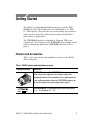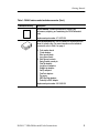
1
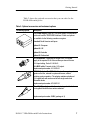
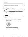
Instructions
P6248
1.7 GHz (Typical)
Differential Probe
071-0566-03
Copyright © Tektronix, Inc. All rights reserved.
Tektronix products are covered by U.S. and foreign patents, issued and
pending. Information in this publication supercedes that in all previously
published material. Specifications and price change privileges reserved.
Tektronix, Inc., P.O. Box 500, Beaverton, OR 97077
TEKTRONIX, TEK, and TEKPROBE are registered trademarks of
Tektronix, Inc.
KlipChip, TwinFoot, TwinTip, and VariTip are trademarks of Tektronix, Inc.
WARRANTY
Tektronix warrants that the products that it manufactures and sells will be free from defects
in materials and workmanship for a period of one (1) year from the date of shipment. If a
product proves defective during this warranty period, Tektronix, at its option, either will
repair the defective product without charge for parts and labor, or will provide a
replacement in exchange for the defective product.
In order to obtain service under this warranty, Customer must notify Tektronix of the defect
before the expiration of the warranty period and make suitable arrangements for the
performance of service. Customer shall be responsible for packaging and shipping the
defective product to the service center designated by Tektronix, with shipping charges
prepaid. Tektronix shall pay for the return of the product to Customer if the shipment is to
a location within the country in which the Tektronix service center is located. Customer
shall be responsible for paying all shipping charges, duties, taxes, and any other charges for
products returned to any other locations.
This warranty shall not apply to any defect, failure or damage caused by improper use or
improper or inadequate maintenance and care. Tektronix shall not be obligated to furnish
service under this warranty a) to repair damage resulting from attempts by personnel other
than Tektronix representatives to install, repair or service the product; b) to repair damage
resulting from improper use or connection to incompatible equipment; c) to repair any
damage or malfunction caused by the use of non-Tektronix supplies; or d) to service a
product that has been modified or integrated with other products when the effect of such
modification or integration increases the time or difficulty of servicing the product.
THIS WARRANTY IS GIVEN BY TEKTRONIX IN LIEU OF ANY OTHER
WARRANTIES, EXPRESS OR IMPLIED. TEKTRONIX AND ITS VENDORS
DISCLAIM ANY IMPLIED WARRANTIES OF MERCHANTABILITY OR
FITNESS FOR A PARTICULAR PURPOSE. TEKTRONIX’ RESPONSIBILITY
TO REPAIR OR REPLACE DEFECTIVE PRODUCTS IS THE SOLE AND
EXCLUSIVE REMEDY PROVIDED TO THE CUSTOMER FOR BREACH OF
THIS WARRANTY. TEKTRONIX AND ITS VENDORS WILL NOT BE LIABLE
FOR ANY INDIRECT, SPECIAL, INCIDENTAL, OR CONSEQUENTIAL
DAMAGES IRRESPECTIVE OF WHETHER TEKTRONIX OR THE VENDOR
HAS ADVANCE NOTICE OF THE POSSIBILITY OF SUCH DAMAGES.
Table of Contents
General Safety Summary . . . . . . . . . . . . . . . . . . . . . . . . . . . .
iii
Preface . . . . . . . . . . . . . . . . . . . . . . . . . . . . . . . . . . . . . . . . . . . .
Contacting Tektronix . . . . . . . . . . . . . . . . . . . . . . . . . . . . . . . . .
v
vi
Getting Started . . . . . . . . . . . . . . . . . . . . . . . . . . . . . . . . . . . . .
Features and Accessories . . . . . . . . . . . . . . . . . . . . . . . . . . . . . .
Installation . . . . . . . . . . . . . . . . . . . . . . . . . . . . . . . . . . . . . . . . .
Instruments with the TEKPROBE Interface (Tektronix TDS 400,
500, 600, and 700 Series Oscilloscopes) . . . . . . . . . . . . . . .
Instruments without the TEKPROBE Interface . . . . . . . . . . . .
1
1
8
9
9
Operating Basics . . . . . . . . . . . . . . . . . . . . . . . . . . . . . . . . . . .
Input Voltage Limits . . . . . . . . . . . . . . . . . . . . . . . . . . . . . . . . .
Maximum Input Voltage . . . . . . . . . . . . . . . . . . . . . . . . . . . . . .
Common-Mode Signal Range . . . . . . . . . . . . . . . . . . . . . . . . . .
Differential-Mode Signal Range . . . . . . . . . . . . . . . . . . . . . . . .
Attenuation Settings . . . . . . . . . . . . . . . . . . . . . . . . . . . . . . . . .
Probe Grounding . . . . . . . . . . . . . . . . . . . . . . . . . . . . . . . . . . . .
Input Impedance and Probe Loading . . . . . . . . . . . . . . . . . . . . .
Common-Mode Rejection . . . . . . . . . . . . . . . . . . . . . . . . . . . . .
Probing Techniques to Maximize CMRR . . . . . . . . . . . . . . . . .
11
11
11
11
12
12
12
14
15
15
Reference . . . . . . . . . . . . . . . . . . . . . . . . . . . . . . . . . . . . . . . . .
Problems with Single-Ended Measurements . . . . . . . . . . . . . . .
Differential Measurements . . . . . . . . . . . . . . . . . . . . . . . . . . . .
Common-Mode Rejection Ratio . . . . . . . . . . . . . . . . . . . . . . . .
Assessing CMRR Error . . . . . . . . . . . . . . . . . . . . . . . . . . . . . . .
Input Impedance Effects on CMRR . . . . . . . . . . . . . . . . . . . . .
Extending the Input Leads . . . . . . . . . . . . . . . . . . . . . . . . . . . . .
Extending the Ground Lead . . . . . . . . . . . . . . . . . . . . . . . . . . . .
Extending the Probe Output . . . . . . . . . . . . . . . . . . . . . . . . . . .
Terminating the Probe . . . . . . . . . . . . . . . . . . . . . . . . . . . . . . . .
Effect of Extending the Output Cable . . . . . . . . . . . . . . . . . . . .
Using the Probe with Other Instruments . . . . . . . . . . . . . . . . . .
17
17
17
18
18
19
19
20
20
20
21
21
Specifications . . . . . . . . . . . . . . . . . . . . . . . . . . . . . . . . . . . . . .
Warranted Characteristics . . . . . . . . . . . . . . . . . . . . . . . . . . . . .
Typical Characteristics . . . . . . . . . . . . . . . . . . . . . . . . . . . . . . .
Nominal Characteristics . . . . . . . . . . . . . . . . . . . . . . . . . . . . . .
23
23
25
28
P6248 1.7 GHz Differential Probe Instructions
i
Table of Contents
List of Figures
ii
Figure 1: Input connector of TEKPROBE interface . . . . . .
8
Figure 2: Using the short ground contact . . . . . . . . . . . . . . .
13
Figure 3: Typical probe input model . . . . . . . . . . . . . . . . . . .
14
Figure 4: Using the input lead accessories to achieve
high CMRR . . . . . . . . . . . . . . . . . . . . . . . . . . . . . . . . . . . . .
15
Figure 5: Using the TwinFoot adapter . . . . . . . . . . . . . . . . . .
16
Figure 6: Simplified model of a differential amplifier . . . . .
18
Figure 7: Twisting the Input Leads . . . . . . . . . . . . . . . . . . . .
20
Figure 8: Typical Common-Mode Rejection Ratio
(B1 and B10 attenuation) . . . . . . . . . . . . . . . . . . . . . . . . . .
26
Figure 9: Typical differential input impedance versus
frequency . . . . . . . . . . . . . . . . . . . . . . . . . . . . . . . . . . . . . . .
26
Figure 10: Probe head and compensation box dimensions .
27
P6248 1.7 GHz Differential Probe Instructions
General Safety Summary
Review the following safety precautions to avoid injury and prevent
damage to this product or any products connected to it. To avoid
potential hazards, use this product only as specified.
Only qualified personnel should perform service procedures.
To Avoid Fire or Personal Injury
Connect and Disconnect Properly. Connect the probe output to the
measurement instrument before connecting the probe to the circuit
under test. Disconnect the probe input and the probe ground from the
circuit under test before disconnecting the probe from the measurement instrument.
Observe All Terminal Ratings. To avoid fire or shock hazard, observe all
ratings and markings on the product. Consult the product manual for
further ratings information before making connections to the product.
Connect the ground lead of the probe to earth ground only.
Do Not Operate Without Covers. Do not operate this product with
covers or panels removed.
Do Not Operate With Suspected Failures. If you suspect there is damage
to this product, have it inspected by qualified service personnel.
Do Not Operate in Wet/Damp Conditions.
Do Not Operate in an Explosive Atmosphere.
Keep Product Surfaces Clean and Dry.
Safety Terms and Symbols
Terms in This Manual. These terms may appear in this manual:
WARNING. Warning statements identify conditions or practices that
could result in injury or loss of life.
P6248 1.7 GHz Differential Probe Instructions
iii
General Safety Summary
CAUTION. Caution statements identify conditions or practices that
could result in damage to this product or other property.
Terms on the Product. These terms may appear on the product:
DANGER indicates an injury hazard immediately accessible as you
read the marking.
WARNING indicates an injury hazard not immediately accessible as
you read the marking.
CAUTION indicates a hazard to property including the product.
Symbols on the Product. These symbols may appear on the product:
CAUTION
Refer to Manual
iv
Protective Ground
(Earth) Terminal
P6248 1.7 GHz Differential Probe Instructions
Preface
This manual contains instructions and specifications for using the
P6248 differential probe.
Related Manuals
For performance verification procedures, adjustment procedures, a
list of replaceable parts, and other service information, refer to the
P6248 Service Manual (071-0573-XX).
P6248 1.7 GHz Differential Probe Instructions
v
Preface
Contacting Tektronix
Phone
1-800-833-9200*
Address
Tektronix, Inc.
Department or name (if known)
14200 SW Karl Braun Drive
P.O. Box 500
Beaverton, OR 97077
USA
Web site
www.tektronix.com
Sales
support
1-800-833-9200, select option 1*
Service
support
1-800-833-9200, select option 2*
Technical
support
Email: [email protected]
1-800-833-9200, select option 3*
6:00 a.m. - 5:00 p.m. Pacific time
*
vi
This phone number is toll free in North America. After office
hours, please leave a voice mail message.
Outside North America, contact a Tektronix sales office or
distributor; see the Tektronix web site for a list of offices.
P6248 1.7 GHz Differential Probe Instructions
Getting Started
The P6248 is a high-bandwidth differential probe with the TEKPROBE interface. The P6248 probe has a bandwidth of 1.5 GHz
(1.7 GHz typical). The probe has low circuit loading, high commonmode rejection, and comes with accessories that accommodate a
wide variety of applications.
The TEKPROBE interface is standard on Tektronix TDS series
oscilloscopes. The Tektronix 1103 TEKPROBE Power Supply can be
used for instruments without the TEKPROBE interface (refer to
page 7).
Features and Accessories
Table 1 shows the features and standard accessories of the P6248
differential probe.
Table 1: P6248 features and standard accessories
Feature/Accessory
Description
TEKPROBE interface. The TEKPROBE interface supplies
power to the probe, selects the correct display scaling, and
automatically sets the 50 Ω termination on the oscilloscope input.
If your oscilloscope does not have the TEKPROBE interface, you
can use the optional 1103 power supply (refer to page 7).
Probe attenuation. The attenuation switch selects either divide
by 1 (÷1) or divide by 10 (÷10).
P6248 1.7 GHz Differential Probe Instructions
1
Getting Started
Table 1: P6248 features and standard accessories (Cont.)
Feature/Accessory
Ground
+
Description
Input connections. The (+), (--), and ground connections of the
probe head accept the standard and optional probe accessories.
You can also plug the head directly onto a pair of 0.025-inch
square pins that have the standard spacing of 0.100-inch on
center.
CAUTION: To avoid damaging the input connectors, do not insert
anything larger than a 0.025-inch square pin into the inputs. To
prolong the life of the connectors, use the tip saver or smooth,
gold-plated pins only.
Instrument case. The instrument case protects the probe from
harsh environments and provides room for storing optional
accessories.
Replacement part number (P6248): 016-1879-XX
Calibration certificate. A certificate of traceable calibration is
provided with every instrument shipped.
Instructions. Provides instructions for operating the P6248
differential probe.
Replacement part number: 071-0566-XX
2
P6248 1.7 GHz Differential Probe Instructions
Getting Started
Table 1: P6248 features and standard accessories (Cont.)
Feature/Accessory
Description
Service manual. Provides procedures for verifying the
performance, adjusting, and maintaining the P6248 differential
probe.
Replacement part number: 071-0573-XX
Probe tip accessory kit. This kit contains the accessories listed
below, in a plastic case. For more information on the individual
accessories, refer to Table 2 on page 4.
10
2
4
2
10
6
4
5
8
8
4
2
4
1
Color marker bands
Y-lead adapters
Short ground leads
Long ground leads
Short ground contacts
Spring-loaded ground pin
TwinTip adapters
Longhorn via adapters
Straight tip adapters
VariTip adapters
TwinFoot adapters
Tip savers
SMT KlipChip adapters
Probe-tip-to-BNC-adapter
Replacement part number: 020-2328-XX
P6248 1.7 GHz Differential Probe Instructions
3
Getting Started
Table 2 describes the contents of the probe tip accessory kit.
Table 2: P6248 Probe tip accessory kit contents
Accessory
Description
Color marker bands
Color marker bands. Attach matching pairs of the color marker
bands onto the cable at the head and compensation box of each
probe. The marker bands enable quick verification of which probe
is connected to which instrument channel.
Replacement part number: 016-1315-00 (package of 10)
Lead set accessory kit. Includes (2) Y-lead adapters,
(4) three-inch ground leads and (2) six-inch ground leads
Replacement part number: 196-3462-00
Y-lead adapter. The Y-lead adapter plugs directly into the probe.
The socketed ends of the leads may be connected to the probe
tips and accessories, or fitted onto 0.025-inch pins.
Ground leads. Use the ground leads for connecting the probe
ground to the circuit. The socketed end of the lead may be
connected to the probe tips and accessories, or fitted onto
0.025-inch pins.
Short ground contact. Use the short ground lead for probing
small geometry components that have a nearby ground point. The
ground easily connects to adjacent square pins when the probe is
plugged directly onto 0.025-inch square pins (0.100-inch spacing).
See Figure 2 on page 13.
Replacement part number: 016-1783-00 (package of 10)
Spring-loaded ground pin. Use the spring-loaded ground when
probing components that have a nearby ground point.
Replacement part number: 016-1782-00 (package of 6)
4
P6248 1.7 GHz Differential Probe Instructions
Getting Started
Table 2: P6248 Probe tip accessory kit contents (Cont.)
Accessory
Description
TwinTip adapter. This accessory provides two adjustable tips for
probing connections that are close to each other.
Replacement part number: 016-1786-00 (package of 4)
Longhorn via adapter. This accessory is similar to the TwinTip
adapter, but it has finer pins for probing smaller holes. Use this
accessory for probing circuit board through-holes (vias).
Replacement part number: 016-1780-00 (package of 5)
Straight tip adapter. The straight tip adapters plug directly into
the probe and allow you to take measurements from two points
spaced 0.100 inches apart. Use the straight tip adapters when
you need to measure fast waveforms that may be affected by the
longer length of other adapters.
Replacement part number: 016-1891-00 (package of 8)
VariTip adapter. The VariTip adapters plug into the probe and
allow you to measure two test points spaced between 0.020 and
0.180 inches apart. Use tweezers to adjust the spacing between
the pins.
Use the VariTip adapters to probe waveforms that have fast rise
times. The short length of the VariTip adapters minimize the
effects of increased probe tip inductance and capacitance on your
measurements.
Replacement part number: 016-1890-00 (package of 8)
TwinFoot adapter. Use the TwinFoot adapter to probe two
adjacent leads on a surface-mount integrated circuit. Flexible
fingers adapt to a range of lead spacings. See Figure 5 on
page 16.
Replacement part number: 016-1785-00 (package of 4)
P6248 1.7 GHz Differential Probe Instructions
5
Getting Started
Table 2: P6248 Probe tip accessory kit contents (Cont.)
Accessory
Description
Tip saver. Use the tip saver to prolong the life of your probe tip
contacts. The tip saver connects to the probe and accepts the
probe tip accessories, bearing the wear of repeated connections
of different probe tips.
Replacement part number: 016-1781-00 (package of 2)
SMT KlipChip adapters. Use this accessory to probe the leads
on dual-in-line packages (DIP).
Replacement part number: 206-0364-XX
Probe-tip-to-BNC adapter. This accessory adapts the probe to a
BNC connector.
Replacement part number: 679-4094-00
6
P6248 1.7 GHz Differential Probe Instructions
Getting Started
Table 3 shows the optional accessories that you can order for the
P6248 differential probe.
Table 3: Optional accessories and instrument options
Accessory/Option
Description
1103 Power supply. Order the 1103 power supply for instruments
that do not have the TEKPROBE Interface. Power cord options
are available for the following countries or regions.
Standard. North America and Japan
Option A1. European
Option A2. UK
Option A3. Australia
Option A5. Switzerland
50 Ω termination. Terminates the output of the 1103 power
supply to the required 50 Ω if the oscilloscope does not have a
50 Ω input setting. Order 011-0049-01.
50 Ω BNC cable. Connects to the 1103 output.
Replacement part number: 012-0076-00
IEEE1394 Adapter. The IEEE1394 Adapter allows you to probe
signals on the bus, external to system enclosures, without
disturbing system operation. The adapter maintains a balanced
55 Ω signal path and can be used in both single-ended and
differential modes.
Replacement part number: 679-5027-00
Micro KlipChip adapters. Use the adapters to probe the leads
on integrated circuits that are surface-mounted.
Replacement part number: SMK4 (package of 4)
P6248 1.7 GHz Differential Probe Instructions
7
Getting Started
Table 3: Optional accessories and instrument options (Cont.)
Accessory/Option
Description
Adjustment tool. Use for making internal adjustments to the
probe. Order 003-0675-01.
Calibration data (Option 95). Option 95, which must be ordered
at the time of purchase, documents the measurements taken
during calibration.
Installation
Before you connect the output of the P6248 differential probe,
determine whether or not your oscilloscope has a TEKPROBE
interface. See Figure 1.
Figure 1: Input connector of TEKPROBE interface
8
P6248 1.7 GHz Differential Probe Instructions
Getting Started
Instruments with the TEKPROBE Interface (Tektronix TDS 400, 500, 600,
and 700 Series Oscilloscopes)
On instruments that have the TEKPROBE interface, simply connect
the probe to the input. The TEKPROBE interface provides power,
selects the correct display scaling, and automatically sets the 50 Ω
termination on the oscilloscope input.
NOTE. TDS 400 and TDS 400A series oscilloscopes do not interpret
the scale factor coding of the P6248 differential probe. This problem
is only apparent when the probe is in the ÷1 position. To correct for
this problem, divide the measurement (or scale factor) by 10 when
you use the probe in the ÷1 position.
Instruments without the TEKPROBE Interface
On instruments that do not have the TEKPROBE interface, you must
order the optional 1103 power supply (refer to page 7). Each 1103
can supply power for two probes. The input of the oscilloscope must
also terminate into 50 Ω. Refer to page 20 for information on the
effects of extending the output of the probe.
When you set the attenuation of the probe, you must factor that
attenuation into your measurement. For example, if the probe is set
at ÷10 and the instrument displays a 0.2 Vp--p signal, the actual
amplitude of the signal is 2 Vp--p.
P6248 1.7 GHz Differential Probe Instructions
9
Getting Started
10
P6248 1.7 GHz Differential Probe Instructions
Operating Basics
This section discusses operating considerations and probing
techniques. For more detailed information about differential
measurements and common-mode rejection ratio (CMRR), see the
Reference section on page 17.
Input Voltage Limits
The P6248 differential probe is designed to probe low-voltage
circuits. Before probing a voltage, take into account the limits for
maximum input voltage, the common-mode signal range, and the
differential-mode signal range.
Maximum Input Voltage
The maximum input voltage is the maximum voltage to ground that
the inputs can withstand without damaging the input circuitry of the
probe.
CAUTION. To avoid damaging the inputs of the P6248 differential
probe, do not apply more than ± 25 V (DC + peak AC) between each
input and ground.
Common-Mode Signal Range
The common-mode signal range is the maximum voltage that you
can apply to each input, with respect to earth ground, without
saturating the input circuitry of the probe. A common-mode voltage
that exceeds the common-mode signal range may produce an
erroneous output waveform even when the differential-mode
specification is met. For Specifications, refer to page 23.
To verify the common-mode signal is within specification, set the
probe to ÷10, temporarily connect one of the probe inputs to
ground, and connect the other probe input to one output of the
P6248 1.7 GHz Differential Probe Instructions
11
Operating Basics
differential signal. Repeat the procedure to test the other output of
the differential signal.
Differential-Mode Signal Range
The differential-mode signal range is the maximum voltage
difference between the (+) and (-- ) inputs that the probe can accept
without distorting the signal. The distortion from a voltage that is too
large can result in an invalid measurement. For Specifications, refer
to page 23.
Attenuation Settings
The differential probe has two attenuation settings: ÷1 and ÷10.
The ÷1 setting provides the best signal-to-noise performance with
low amplitude signals. The ÷10 setting increases the differentialmode signal range by a factor of 10.
Probe Grounding
In addition to the (+) and (-- ) inputs on the probe head, there is also a
ground (common) input. (See Figures 2 and 3.)
CAUTION. To avoid damaging the circuitry under test, connect the
probe ground (common) to a ground-reference point only.
You can use the probe to take a differential measurement regardless
of whether or not the ground (common) is connected.
There are some applications that may require a ground reference
connection to maintain measurement accuracy. Generally this is
necessary when probing circuits which are fully isolated from ground
such as battery operated devices. In most applications, however, the
common-mode impedance to ground is greater than the differential
impedance. Hence, adding the probe ground lead does not improve
the high-frequency performance of the measurement.
12
P6248 1.7 GHz Differential Probe Instructions
Operating Basics
In addition to the 6-inch ground lead, there are other ground lead
accessories that are useful in certain applications. Figure 2 shows
how to use the short ground contact. Figure 4 on page 15 shows the
spring-loaded ground pin.
Figure 2: Using the short ground contact
P6248 1.7 GHz Differential Probe Instructions
13
Operating Basics
Input Impedance and Probe Loading
When you connect the probe inputs to a circuit, you are introducing a
new resistance, capacitance, and inductance into the circuit. Each
input of the P6248 differential probe has a characteristic input
impedance of 100 kΩ to ground in parallel with less than 1 pF. See
Figure 3.
For signals with low source impedance and frequency, the 100 kΩ
input impedance on each input is large enough to prevent the inputs
from loading the signal sources. The greater the source impedances
and the higher the signal frequencies, the more you should take these
factors into account.
+ Input
1.5 pF
100 kΩ
Ground
1.5 pF
0.25
pF
100 kΩ
- Input
Figure 3: Typical probe input model
As the impedance of the signal source on an input increases, the
more the probe loads the source and reduces the signal amplitude.
The frequency of the signal also affects signal measurement. As the
frequency of the signal increases, the input impedance of the probe
decreases. The lower the impedance of the probe relative to that of
the source, the more the probe loads the circuit under test and
reduces the signal amplitude. For a graph of frequency versus input
impedance, refer to Figure 9 on page 26.
14
P6248 1.7 GHz Differential Probe Instructions
Operating Basics
Common-Mode Rejection
The common-mode rejection ratio (CMRR) is the specified ability of
a P6248 differential probe to reject signals that are common to both
inputs. More precisely, CMRR is the ratio of the differential gain to
the common-mode gain. The higher the ratio, the greater the ability
to reject common-mode signals.
Common-mode rejection decreases as the input frequency increases.
Figure 8 on page 26 is a plot of typical CMRR of the probe versus
input frequency. For a more extended discussion of CMRR, see
page 18.
Probing Techniques to Maximize CMRR
The common-mode rejection of the probe is highest when using the
accessories shown in Figures 4 and 5. These accessories minimize
the distance between the probe head and the signal source.
Figure 4: Using the input lead accessories to achieve high CMRR
P6248 1.7 GHz Differential Probe Instructions
15
Operating Basics
IC pads being probed
Conductive side
of probe tip
Insulated side
of probe tip
Figure 5: Using the TwinFoot adapter
16
P6248 1.7 GHz Differential Probe Instructions
Reference
This section contains important reference information about
differential measurements and how to increase the accuracy of your
measurements.
Problems with Single-Ended Measurements
While suitable in many applications, single-ended measurements can
present problems in the following situations:
H When the signal is not referenced to earth ground
H When connecting or disconnecting the probe ground distorts the
signal
H When connecting the signal reference to ground damages or
upsets the circuit
Differential Measurements
Devices designed to make differential measurements avoid the
problems posed by single-ended systems. These devices include a
variety of differential probes, differential amplifiers, and isolators.
The differential amplifier (Figure 6) is at the heart of any device or
system designed to make differential measurements. Ideally, the
differential amplifier rejects any voltage that is common to the inputs
and amplifies any difference between the inputs. Voltage that is
common to both inputs is often referred to as the Common-Mode
Voltage (VCM) and voltage that is different as the Differential-Mode
Voltage (VDM).
P6248 1.7 GHz Differential Probe Instructions
17
Reference
+
Vout
+
-
Differential
mode VDM
+
Common
V
mode CM
Figure 6: Simplified model of a differential amplifier
Common-Mode Rejection Ratio
In reality, differential amplifiers cannot reject all of the commonmode signal. The ability of a differential amplifier to reject the
common-mode signal is expressed as the Common-Mode Rejection
Ratio (CMRR). The CMRR is the differential-mode gain (ADM)
divided by the common-mode gain (ACM). It is expressed either as a
ratio or in dB.
CMRR =
A DM
A CM
dB = 20 log
V DM
V CM
CMRR generally is highest (best) at DC and degrades with
increasing frequency.
Assessing CMRR Error
Figure 8 on page 26 shows the CMRR of the P6248 differential
probe. This derating chart assumes a common-mode signal that is
sinusoidal.
18
P6248 1.7 GHz Differential Probe Instructions
Reference
A quick way to assess the magnitude of CMRR error when the
common-mode signal is not sinusoidal is to connect both leads to the
same point in the circuit. The oscilloscope will display only the
common-mode component which is not fully rejected by the probe.
While this technique may not give you entirely accurate measurements, it does allow you to determine if the magnitude of the
common-mode error signal is significant.
Input Impedance Effects on CMRR
The lower the input impedance of the probe relative to the source
impedance, the lower the CMRR. See Figure 9 on page 26.
Significant differences in the source impedance driving the two
inputs will also lower the CMRR.
Extending the Input Leads
At times it may be necessary to extend the probe inputs with wires or
a probe tip adapter. When you do this, you should minimize the lead
lengths to optimize common-mode rejection and twist the input leads
together as shown in Figure 7.
Twisting the input leads together does increase capacitance that may
degrade high-frequency performance. You should take into account
any effects caused by the extended leads when you take a measurement.
CAUTION. To avoid damaging the input connectors, do not insert
anything larger than a 0.025-inch square pin into the inputs. Use the
tip saver accessory to preserve the integrity of the input connectors.
P6248 1.7 GHz Differential Probe Instructions
19
Reference
Figure 7: Twisting the Input Leads
Extending the Ground Lead
Extending the ground lead will have little, if any, affect on your
measurements. In most circuits, the ground path from the differential
source has sufficiently high impedance to damp out any ringing
caused by lead inductance.
Extending the Probe Output
With the 1103 TEKPROBE power supply, it is possible to extend the
output of the probe in order to connect the probe to other types of
measurement instruments or simply to connect the probe to a signal
source that is outside the reach of the probe.
Terminating the Probe
The probe must terminate into 50 Ω at the input of the measurement
instrument. Use the 1103 TEKPROBE power supply to adapt the
differential probe and set the input impedance of the measurement
instrument to 50 Ω. If the measurement instrument does not support
50 Ω input termination, connect a 50 Ω coaxial terminator on the
input.
20
P6248 1.7 GHz Differential Probe Instructions
Reference
Effect of Extending the Output Cable
As the frequency of a signal increases, current flow concentrates at
the outer edges of the conductor, effectively increasing the
impedance. This effect is known as skin loss. The P6248 probe
contains circuitry to compensate for skin loss.
The compensation provides flat response with the probe cable.
Extending the length of the output cable increases the amount of skin
loss beyond the range of compensation correction. Minimizing the
length of cable extension reduces the attenuation.
In critical applications which require high amplitude accuracy, you
should first characterize the response of the probe with the extension
using a leveled signal source and power meter. Then, you can factor
the characterization results into the measurement.
Using the Probe with Other Instruments
Besides the oscilloscope, it is possible to use the P6248 differential
probe with other types of measurement instruments, such as
spectrum analyzers, time internal analyzers, and network analyzers.
When using the differential probes with these instruments you must
normalize the probe with the instrument before making a measurement.
P6248 1.7 GHz Differential Probe Instructions
21
Reference
22
P6248 1.7 GHz Differential Probe Instructions
Specifications
The specifications in Tables 4 through 7 apply to a P6248 probe
installed on a Tektronix TDS 694C oscilloscope. When the probe is
used with another oscilloscope, the oscilloscope must have an input
impedance of 50 Ω. The probe must have a warm-up period of at
least 20 minutes and be in an environment that does not exceed the
limits described in Table 4. Specifications for the P6248 differential
probe fall into three categories: warranted, typical, and nominal
characteristics.
Warranted Characteristics
Warranted characteristics (Table 4) describe guaranteed performance
within tolerance limits or certain type-tested requirements.
Warranted characteristics that have checks in the Performance
Verification section of the service manual are marked with the
n symbol.
Table 4: Warranted electrical characteristics
Characteristic
Description
n DC attenuation accuracy
± 2% for input voltages as follows:
± 750 mV (÷1) and ± 7.5 V (÷10)
± 5% for input voltages as follows:
± 850 mV (÷1) and ± 8.5 V (÷10)
Maximum non destructive input voltage
± 25 V(DC + peak AC) between signal and
common of the same channel.
n Differential signal range (DC coupled)
± 8.5 V at attenuation setting of ÷10
± 850 mV at attenuation setting of ÷1
Common-mode signal range (DC coupled)
±7V
P6248 1.7 GHz Differential Probe Instructions
23
Specifications
Table 4: Warranted electrical characteristics (Cont.)
Characteristic
Description
n Output offset voltage
± 10 mV (+ 20_ C to + 30_ C,
+ 68_ F to + 86_ F)
± 50 mV (0_ C to + 60_ C,
+ 32_ F to + 122_ F)
n Rise time (probe only)
< 265 ps
n Common-mode rejection
j
ratio
45 dB at 1 MHz in ÷10
25 dB at 100 MHz in ÷10
20 dB at 500 MHz in ÷10
18 dB at 1 GHz in ÷10
60 dB at 1 MHz in ÷1
38 dB at 100 MHz in ÷1
35 dB at 500 MHz in ÷1
30 dB at 1 GHz in ÷1
Bandwidth (probe only)
DC to ≥ 1.5 GHz (-- 3dB)
Temperature
Operating: 0 to + 50_ C
(+ 32 to + 122_ F)
0 to + 60_ C
(+ 32 to + 140_ F)1 (probe head)
Nonoperating: -- 55 to + 75_ C
(-- 131 to + 167_ F)1
Humidity
Operating: 0--90% RH, tested at
+ 30 to + 50_ C (+ 68 to + 122_ F)
Nonoperating: 0--90% RH, tested at
+ 30 to + 60_ C (+ 68 to + 140_ F)
1
See warning that follows.
WARNING. To avoid a burn hazard at high ambient temperatures, do
not touch the probe with bare hands at operating temperatures above
+ 50_ C or at nonoperating temperatures above + 70_ C. Allow
sufficient time for the probe to cool before handling.
24
P6248 1.7 GHz Differential Probe Instructions
Specifications
Typical Characteristics
Typical characteristics (Tables 5 and 6) describe typical but not
guaranteed performance.
Table 5: Typical electrical characteristics
Characteristic
Description
Differential input resistance, DC coupled
200 kΩ ± 2%
Common-mode input resistance, DC
coupled
100 kΩ ± 2%
Differential input capacitance
< 1 pF at 1 MHz
Common-mode input capacitance
< 2 pF at 1 MHz
Harmonic distortion
≤ 1.5% measured using 354 mVRMS (or
1.0 VP-P) output at 100 MHz
Differential offset range
± 700 mV (÷ 1)
± 7 V (÷ 10)
Common-mode rejection ratio
See Figure 8
Bandwidth (probe only)
DC to ≥ 1.7 GHz (-- 3dB) @ ≤27_ C (÷1)
DC to ≥ 1.85 GHz (-- 3dB) @ ≤27_ C
(÷10)
Random noise
Input impedance
Pass band ripple
< 50 nV ᎩHz at 100 MHz
See Figure 9
≤ ± 0.25 dB to the 3 dB bandwidth (deviation from a nominal slope)
P6248 1.7 GHz Differential Probe Instructions
25
Specifications
80
60
dB
40
÷1
÷10
20
0
0
300 M
600 M
900 M
1.2 G
1.5 G
1.8 G
2G
Frequency (Hz)
Figure 8: Typical Common-Mode Rejection Ratio (÷1 and ÷10
attenuation)
Impedance (Ω)
100 k
10 k
1k
100
10
0
250 M
500 M
750 M
1G
1 .25 G
Frequency (Hz)
1 .50 G
1 .75 G
2G
Figure 9: Typical differential input impedance versus frequency
The graph in Figure 9 represents simulation results of a first order
model of the probe input.
26
P6248 1.7 GHz Differential Probe Instructions
Specifications
Table 6: Typical mechanical characteristics
Dimensions, input connection
0.63 mm (0.025 in) square pin on 2.54 mm
(0.100 in) centers
Dimensions, control box
107 mm × 41 mm × 26 mm
(4.2 in × 1.6 in × 1.0 in)
Dimensions, probe head
78 mm × 12 mm × 9.3 mm
(3.0 in × 0.47 in × 0.36 in)
Dimensions, output cable
1.2 m (47 in)
Unit weight (probe only)
160 g (5.4 oz)
1.6 in
.47 in
3.0 in
.36 in
1.0 in
4.2 in
Figure 10: Probe head and compensation box dimensions
P6248 1.7 GHz Differential Probe Instructions
27
Specifications
Nominal Characteristics
Nominal characteristics (Table 7) describe guaranteed traits, but the
traits do not have tolerance limits.
Table 7: Nominal electrical characteristics
Input configuration
Differential (two inputs, + and -- ), with case
ground
Output coupling
DC
Attenuation settings
÷1 and ÷10
Termination
Terminate output into 50 Ω
28
P6248 1.7 GHz Differential Probe Instructions