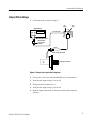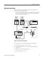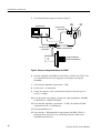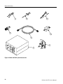
1
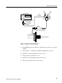
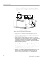
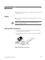
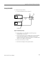
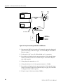
Service Manual
P6246 400 MHz & P6247 1 GHz
Differential Probes
070-9899-03
Warning
The servicing instructions are for use by qualified
personnel only. To avoid personal injury, do not
perform any servicing unless you are qualified to
do so. Refer to all safety summaries prior to
performing service.
*P070989903*
070989903
Copyright © Tektronix, Inc. All rights reserved.
Tektronix products are covered by U.S. and foreign patents, issued and pending. Information in this publication supercedes
that in all previously published material. Specifications and price change privileges reserved.
Tektronix, Inc., 14200 SW Karl Braun Drive, Beaverton, OR 97077
TEKTRONIX and TEK are registered trademarks of Tektronix, Inc.
WARRANTY
Tektronix warrants that the products that it manufactures and sells will be free from defects in materials and workmanship
for a period of one (1) year from the date of shipment. If a product proves defective during this warranty period, Tektronix,
at its option, either will repair the defective product without charge for parts and labor, or will provide a replacement in
exchange for the defective product.
In order to obtain service under this warranty, Customer must notify Tektronix of the defect before the expiration of the
warranty period and make suitable arrangements for the performance of service. Customer shall be responsible for
packaging and shipping the defective product to the service center designated by Tektronix, with shipping charges prepaid.
Tektronix shall pay for the return of the product to Customer if the shipment is to a location within the country in which the
Tektronix service center is located. Customer shall be responsible for paying all shipping charges, duties, taxes, and any
other charges for products returned to any other locations.
This warranty shall not apply to any defect, failure or damage caused by improper use or improper or inadequate
maintenance and care. Tektronix shall not be obligated to furnish service under this warranty a) to repair damage resulting
from attempts by personnel other than Tektronix representatives to install, repair or service the product; b) to repair
damage resulting from improper use or connection to incompatible equipment; c) to repair any damage or malfunction
caused by the use of non-Tektronix supplies; or d) to service a product that has been modified or integrated with other
products when the effect of such modification or integration increases the time or difficulty of servicing the product.
THIS WARRANTY IS GIVEN BY TEKTRONIX IN LIEU OF ANY OTHER WARRANTIES, EXPRESS OR
IMPLIED. TEKTRONIX AND ITS VENDORS DISCLAIM ANY IMPLIED WARRANTIES OF
MERCHANTABILITY OR FITNESS FOR A PARTICULAR PURPOSE. TEKTRONIX’ RESPONSIBILITY TO
REPAIR OR REPLACE DEFECTIVE PRODUCTS IS THE SOLE AND EXCLUSIVE REMEDY PROVIDED TO
THE CUSTOMER FOR BREACH OF THIS WARRANTY. TEKTRONIX AND ITS VENDORS WILL NOT BE
LIABLE FOR ANY INDIRECT, SPECIAL, INCIDENTAL, OR CONSEQUENTIAL DAMAGES IRRESPECTIVE
OF WHETHER TEKTRONIX OR THE VENDOR HAS ADVANCE NOTICE OF THE POSSIBILITY OF SUCH
DAMAGES.
Table of Contents
P6246 & P6247 Service Manual
General Safety Summary . . . . . . . . . . . . . . . . . . . . . . . . . . . . . . . . . . .
Preface . . . . . . . . . . . . . . . . . . . . . . . . . . . . . . . . . . . . . . . . . . . . . . . . . . .
iii
v
Related Manuals . . . . . . . . . . . . . . . . . . . . . . . . . . . . . . . . . . . . . . . . . . . . . . . . .
Contacting Tektronix . . . . . . . . . . . . . . . . . . . . . . . . . . . . . . . . . . . . . . . . . . . . .
v
v
Specifications . . . . . . . . . . . . . . . . . . . . . . . . . . . . . . . . . . . . . . . . . . . . .
1
Warranted Characteristics . . . . . . . . . . . . . . . . . . . . . . . . . . . . . . . . . . . . . . . . . .
Typical Characteristics . . . . . . . . . . . . . . . . . . . . . . . . . . . . . . . . . . . . . . . . . . . .
Nominal Characteristics . . . . . . . . . . . . . . . . . . . . . . . . . . . . . . . . . . . . . . . . . . .
1
2
4
Performance Verification . . . . . . . . . . . . . . . . . . . . . . . . . . . . . . . . . . .
5
Equipment Required . . . . . . . . . . . . . . . . . . . . . . . . . . . . . . . . . . . . . . . . . . . . . .
Preparation . . . . . . . . . . . . . . . . . . . . . . . . . . . . . . . . . . . . . . . . . . . . . . . . . . . . .
Output Offset Voltage . . . . . . . . . . . . . . . . . . . . . . . . . . . . . . . . . . . . . . . . . . . . .
DC Attenuation Accuracy . . . . . . . . . . . . . . . . . . . . . . . . . . . . . . . . . . . . . . . . .
Differential Signal Range . . . . . . . . . . . . . . . . . . . . . . . . . . . . . . . . . . . . . . . . . .
Analog Bandwidth . . . . . . . . . . . . . . . . . . . . . . . . . . . . . . . . . . . . . . . . . . . . . . .
Common Mode Rejection Ratio . . . . . . . . . . . . . . . . . . . . . . . . . . . . . . . . . . . . .
TekProbe Communication (operational check) . . . . . . . . . . . . . . . . . . . . . . . . .
5
6
7
8
9
11
13
14
Adjustment Procedures . . . . . . . . . . . . . . . . . . . . . . . . . . . . . . . . . . . . .
17
Equipment Required . . . . . . . . . . . . . . . . . . . . . . . . . . . . . . . . . . . . . . . . . . . . . .
Offset (preliminary) . . . . . . . . . . . . . . . . . . . . . . . . . . . . . . . . . . . . . . . . . . . . . .
Gain . . . . . . . . . . . . . . . . . . . . . . . . . . . . . . . . . . . . . . . . . . . . . . . . . . . . . . . . . . .
Offset (Final) . . . . . . . . . . . . . . . . . . . . . . . . . . . . . . . . . . . . . . . . . . . . . . . . . . .
DC CMRR . . . . . . . . . . . . . . . . . . . . . . . . . . . . . . . . . . . . . . . . . . . . . . . . . . . . .
AC CMRR . . . . . . . . . . . . . . . . . . . . . . . . . . . . . . . . . . . . . . . . . . . . . . . . . . . . .
17
18
20
21
21
23
Maintenance . . . . . . . . . . . . . . . . . . . . . . . . . . . . . . . . . . . . . . . . . . . . . .
25
Cleaning . . . . . . . . . . . . . . . . . . . . . . . . . . . . . . . . . . . . . . . . . . . . . . . . . . . . . . .
Replacing TekProbe Interface Pins . . . . . . . . . . . . . . . . . . . . . . . . . . . . . . . . . .
Removing and Replacing the TekProbe Interface Collar . . . . . . . . . . . . . . . . .
25
25
26
Options . . . . . . . . . . . . . . . . . . . . . . . . . . . . . . . . . . . . . . . . . . . . . . . . . .
Replaceable Parts . . . . . . . . . . . . . . . . . . . . . . . . . . . . . . . . . . . . . . . . . .
Appendix A: Alternate Verification Procedures . . . . . . . . . . . . . . . . .
27
29
37
Equipment Required . . . . . . . . . . . . . . . . . . . . . . . . . . . . . . . . . . . . . . . . . . . . . .
Preparation . . . . . . . . . . . . . . . . . . . . . . . . . . . . . . . . . . . . . . . . . . . . . . . . . . . . .
Analog Bandwidth . . . . . . . . . . . . . . . . . . . . . . . . . . . . . . . . . . . . . . . . . . . . . . .
CMRR (Common Mode Rejection Ratio) . . . . . . . . . . . . . . . . . . . . . . . . . . . . .
37
38
39
41
i
Table of Contents
List of Figures
Figure 1: Typical Common-Mode Rejection Ratio
(÷ 1 and ÷ 10 attenuation) . . . . . . . . . . . . . . . . . . . . . . . . . . . . . .
Figure 2: Typical input impedance versus frequency . . . . . . . . . . . .
Figure 3: Setup for the output offset voltage test . . . . . . . . . . . . . . . .
Figure 4: Setup for differential- mode tests . . . . . . . . . . . . . . . . . . . . .
Figure 5: Set up for analog bandwidth test and CMRR . . . . . . . . . .
Figure 6: Adjustment locations . . . . . . . . . . . . . . . . . . . . . . . . . . . . . . .
Figure 7: Setup for the offset adjustment . . . . . . . . . . . . . . . . . . . . . .
Figure 8: Setup for gain adjustment . . . . . . . . . . . . . . . . . . . . . . . . . .
Figure 9: Setup for DC CMRR and AC CMRR adjustments . . . . . .
Figure 10: Replacing TekProbe interface pins . . . . . . . . . . . . . . . . . .
Figure 11: Replacing the TekProbe collar . . . . . . . . . . . . . . . . . . . . . .
Figure 12: P6246 and P6247 replaceable parts . . . . . . . . . . . . . . . . . .
Figure 13: P6246 and P6247 standard accessories . . . . . . . . . . . . . . .
Figure 14: P6246 and P6247 optional accessories . . . . . . . . . . . . . . . .
Figure 15: Normalizing the setup . . . . . . . . . . . . . . . . . . . . . . . . . . . . .
Figure 16: Setup for the analog bandwidth and CMRR tests . . . . . .
ii
3
4
7
9
12
18
19
20
22
25
26
29
32
34
39
40
P6246 & P6247 Service Manual
General Safety Summary
Review the following safety precautions to avoid injury and prevent damage to
this product or any products connected to it. To avoid potential hazards, use this
product only as specified.
Only qualified personnel should perform service procedures.
To Avoid Fire or
Personal Injury
Ground the Product. This product is indirectly grounded through the grounding
conductor of the mainframe power cord. To avoid electric shock, the grounding
conductor must be connected to earth ground. Before making connections to the
input or output terminals of the product, ensure that the product is properly
grounded.
Observe All Terminal Ratings. To avoid fire or shock hazard, observe all ratings
and markings on the product. Consult the product manual for further ratings
information before making connections to the product.
The common terminal is at ground potential. Do not connect the common
terminal to elevated voltages.
Do not apply a potential to any terminal, including the common terminal, that
exceeds the maximum rating of that terminal.
Do Not Operate With Suspected Failures. If you suspect there is damage to this
product, have it inspected by qualified service personnel.
Do Not Operate in Wet/Damp Conditions.
Do Not Operate in an Explosive Atmosphere.
Keep Product Surfaces Clean and Dry.
P6246 & P6247 Service Manual
iii
General Safety Summary
Symbols and Terms
Terms in this Manual. These terms may appear in this manual:
WARNING. Warning statements identify conditions or practices that could result
in injury or loss of life.
CAUTION. Caution statements identify conditions or practices that could result in
damage to this product or other property.
Terms on the Product. These terms may appear on the product:
DANGER indicates an injury hazard immediately accessible as you read the
marking.
WARNING indicates an injury hazard not immediately accessible as you read the
marking.
CAUTION indicates a hazard to property including the product.
Symbols on the Product. The following symbols may appear on the product:
WARNING
High Voltage
iv
Protective Ground
(Earth) Terminal
CAUTION
Refer to Manual
Double
Insulated
P6246 & P6247 Service Manual
Preface
This manual contains specifications and service information for the P6246 and
P6247 differential probes.
Related Manuals
For operating information, refer to the P6246 & P6247 Instructions
(070-9898-XX).
Contacting Tektronix
Product
Support
For questions about using Tektronix measurement products, call
toll free in North America:
1-800-TEK-WIDE (1-800-835-9433 ext. 2400)
6:00 a.m. -- 5:00 p.m. Pacific time
Or contact us by e-mail:
[email protected]
For product support outside of North America, contact your
local Tektronix distributor or sales office.
Service
Support
Tektronix offers extended warranty and calibration programs as
options on many products. Contact your local Tektronix
distributor or sales office.
For a listing of worldwide service centers, visit our web site.
P6246 & P6247 Service Manual
For other
information
In North America:
1-800-TEK-WIDE (1-800-835-9433)
An operator will direct your call.
To write us
Tektronix, Inc.
14200 SW Karl Braun Drive
Beaverton, OR 97077
USA
Website
Tektronix.com
v
Preface
vi
P6246 & P6247 Service Manual
Specifications
The specifications in Tables 1 through 4 apply to a P6246 or P6247 differential
probe installed on a Tektronix TDS 784A oscilloscope. When the probe is used
with another oscilloscope, the oscilloscope must have an input impedance of
50 Ω and a bandwidth of 1 GHz. The probe must have a warm-up period of at
least 20 minutes and be in an environment that does not exceed the limits
described in Table 1. Specifications for the P6246 and P6247 differential probes
fall into three categories: warranted, typical, and nominal characteristics.
Warranted Characteristics
Warranted characteristics (Table 1) describe guaranteed performance within
tolerance limits or certain type-tested requirements. Warranted characteristics
that have checks in the Performance Verification section are marked with the
n symbol.
Table 1: Warranted electrical characteristics
n DC attenuation accuracy
± 2% for input voltages ± 750 mV (÷ 1) and ± 7.5 V (÷ 10)
± 5% for input voltages ± 850 mV (÷ 1) and ± 8.5 V (÷ 10)
Maximum non destructive input voltage
± 25 V(DC + peak AC) between signal and common of the same channel
n Differential signal range (DC coupled)
± 8.5 V at attenuation setting of ÷ 10
± 850 mV at attenuation setting of ÷ 1
Common-mode signal range (DC coupled)
±7V
n Output offset voltage
± 10 mV (+ 20_ C to + 30_ C)
± 50 mV (0_ C to + 60_ C)
Rise time (probe only)
P6246: < 875 ps
P6247: < 350 ps
n Common-mode rejection
j
ratio
45 dB at 1 MHz in ÷ 10
25 dB at 100 MHz in ÷ 10
20 dB at 500 MHz in ÷ 10
18 dB at 1 GHz in ÷ 10
60 dB at 1 MHz in ÷ 1
38 dB at 100 MHz in ÷ 1
35 dB at 500 MHz in ÷ 1
30 dB at 1 GHz in ÷ 1
n Bandwidth (probe only)
P6246: DC to ≥ 400 MHz (-- 3dB)
P6247: DC to ≥ 1 GHz (-- 3dB)
Temperature
Operating: 0 to + 50_ C, 0 to + 60_ C1 (probe head)
Nonoperating: - 55 to + 75_ C1
P6246 & P6247 Service Manual
1
Specifications
Table 1: Warranted electrical characteristics (cont.)
Operating: 0-- 90% RH, tested at + 30 to + 50_ C
Nonoperating: 0-- 90% RH, tested at + 30 to + 60_ C
Humidity
1
See warning that follows.
WARNING. To avoid a burn hazard at high ambient temperatures, do not touch
the probe with bare hands at operating temperatures above + 50_ C or at
nonoperating temperatures above + 70_ C.
Typical Characteristics
Typical characteristics (Tables 2 and 3) describe typical but not guaranteed
performance.
Table 2: Typical electrical characteristics
Differential input resistance, DC coupled
200 kΩ
Input resistance, DC coupled
100 kΩ ± 2%
Differential input capacitance
< 1 pF at 1 MHz
Common-mode input capacitance
< 2 pF at 1 MHz
Harmonic distortion
≤ 1.5% measured using 495 mVRMS (or 1.4 VP-P) output at 100 MHz
Differential offset range
± 700 mV (÷ 1 setting)
± 7 V (÷ 10 setting)
Common mode rejection ratio
See Figure 1
Random noise
< 50 nV Hz at 100 MHz
Input impedance
See Figure 2
Bandwidth limit
- 3 dB at 200 MHz
DC reject bandwidth
- 3 dB at 4 Hz (÷ 10 setting)
- 3 dB at 0.4 Hz (÷ 1 setting)
Pass band ripple
P6246: ≤ ± 0.25 dB to the 3 dB bandwidth (deviation from a nominal slope)
P6247: ≤ ± 0.25 dB to 850 MHz (deviation from a nominal slope)
2
P6246 & P6247 Service Manual
Specifications
100
P6246
80
60
dB
÷1
40
÷10
20
0
0
200
400
600
800
1000
MHz
P6247
80
60
dB
40
÷1
÷10
20
0
0
200
400
600
800
1000
MHz
Figure 1: Typical Common-Mode Rejection Ratio (÷ 1 and ÷ 10 attenuation)
P6246 & P6247 Service Manual
3
Specifications
Impedance
(Ω)
100 k
10 k
1k
100
10
0
250 M
500 M
Frequency (Hz)
750 M
1G
Figure 2: Typical input impedance versus frequency
Table 3: Typical mechanical characteristics
Dimensions, input connection
0.63 mm (0.025 in) square pin on 2.54 mm (0.100 in) centers
Dimensions, control box
107 mm × 41 mm × 26 mm
(4.2 in × 1.6 in × 1.0 in)
Dimensions, probe head
78 mm × 12 mm × 9.3 mm
(3.0 in × 0.47 in × 0.36 in)
Dimensions, output cable
1.2 m (47 in)
Unit weight (probe only)
160 g (5.4 oz)
Nominal Characteristics
Nominal characteristics (Table 4) describe guaranteed traits, but the traits do not
have tolerance limits.
Table 4: Nominal electrical characteristics
Input configuration
Differential (two inputs, + and - ), with case ground
Output coupling
DC and DC Reject
Attenuation settings
÷1 and ÷10
Termination
Terminate output into 50 Ω
4
P6246 & P6247 Service Manual
Performance Verification
Use the following procedures to verify the warranted specifications of the P6246
and P6247 Differential Probes. Before beginning these procedures, refer to
page 15 and photocopy the test record and use it to record the performance test
results. The recommended calibration interval is one year.
These procedures test the following specifications:
H
DC attenuation accuracy
H
Differential signal range
H
Output offset voltage
H
Analog bandwidth
H
Common mode rejection ratio
Equipment Required
Table 5 lists the equipment required to perform the performance verification
procedure. The types and quantities of connectors may vary depending on the
specific equipment you use.
NOTE. The procedures in this section require a network analyzer to perform the
analog bandwidth and CMRR tests. While a network analyzer is recommended
for these procedures, it is not always feasible to obtain a suitable model. For
alternative procedures that do not require a network analyzer, refer to Appendix A on page 37.
Table 5: Test equipment
P6246 & P6247 Service Manual
Description
Minimum requirements
Example product
Calibrated DC voltage
source (2 required)
Adjustable from 0 V to ≥ 17 V.
Tektronix PS280
Outputs must be isolated from
earth ground. DC bench supplies
monitored with DMM are adequate.
DMM (2 required)
DC Accuracy ≥ 0.5% on range to
measure 8.5 V, averaging mode.
Tektronix DMM916
Network analyzer
100 kHz to ≥ 2 GHz, with cables
and adapters to BNC male
Hewlett Packard 8753D
5
Performance Verification
Table 5: Test equipment (cont.)
Description
Minimum requirements
Example product
Digitizing oscilloscope with
TekProbe interface
Fully compatible with TekProbe II
interface (needed only for functional check of the TekProbe interface)
Tektronix TDS 500, 600, or
700 series oscilloscope
TekProbe Power Supply
Tektronix Type 1103
Tektronix Type 1103
BNC cables (2)
50 Ω, 42 inch
012-0057-01
Banana-to-banana patch
cords (3)
2 red
012-0031-00
1 black
012-0039-00
Dual-male-banana-to-female BNC adapter (3)
As per description
103-0090-00
BNC male to dual binding
post adapter (2)
As per description
103-0035-00
0.025” square pins (3)
Approximately 3/4 inch long,
smooth, gold plated.
Precision inline BNC
terminator
50 Ω ± 0.1%
011-0129-00
Probe tip adapters
Y-lead
BNC to probe tip
probe ground lead
(included in the standard probe tip
accessory kit)
020-2203-01
Preparation
Prepare the equipment as follows:
1. Connect the y-lead adapter to the inputs of the probe and the ground lead to
the probe ground. (For a description of these accessories, refer to the list of
standard accessories on pages 31 and 32.)
2. Attach the probe to the 1103 TekProbe power supply.
3. If necessary, set the line selector of the 1103 power supply to the correct
voltage.
4. Turn on the 1103 power supply.
5. Set the 1103 offset to off (button not illuminated).
6. Allow the probe and test equipment to warm up for 20 minutes at an ambient
temperature of 20_ C to 30_ C.
Perform the verification procedures in order.
6
P6246 & P6247 Service Manual
Performance Verification
Output Offset Voltage
1. Connect the probe as shown in Figure 3.
CH 1
output
CH 1
input
Digital multimeter
50 Ω BNC cable
+
1103
--
Female BNC to male
banana adapter
50 Ω precision
terminator
P6246/7
BNC to probe tip adapter
DM pair for offset test
Figure 3: Setup for the output offset voltage test
2. Set the probe to DC reject off, full bandwidth, and ÷ 10 attenuation.
3. Verify that the output voltage is ≤ ± 10 mV.
4. Change the probe attenuation to ÷ 1.
5. Verify that the output voltage is ≤ ± 10 mV.
6. Keep the output connections for the next procedure (DC attenuation
accuracy).
P6246 & P6247 Service Manual
7
Performance Verification
DC Attenuation Accuracy
1. Connect the probe input to the y-lead adapter and then to the DC source.
Monitor the source voltage with the DMM.
2. Set the probe to DC reject off, full bandwidth, and ÷ 10 attenuation.
3. Set the input voltage on the DC source to approximately 5 V. Record the
actual voltage as Vin1.
4. Record the output voltage as Vout1.
5. Set the input voltage on the DC source to approximately 1 V. Record the
actual voltage as Vin2.
6. Record the output voltage as Vout2.
7. Calculate the attenuation as follows: (Vin1 -- Vin2) ÷ (Vout1 -- Vout2).
8. Verify that the attenuation is in the range of 9.8 to 10.2.
9. Set input voltage on the DC source to approximately 0.5 V. Record the actual
voltage as Vin1.
10. Change the attenuation to ÷ 1.
11. Record the output voltage as Vout1.
12. Set input voltage on DC source to approximately 0.1 V. Record the actual
voltage as Vin2.
13. Record the output voltage as Vout2.
14. Calculate the attenuation as follows: (Vin1 -- Vin2) ÷ (Vout1 -- Vout2).
15. Verify that the attenuation is in the range of 0.98 to 1.02.
16. Turn DC reject on.
17. Verify that the output returns to approximately 0 volts. (This is a functional
check; there is no specified performance limit.)
18. Turn DC reject off.
19. Keep the output connections for the next procedure.
8
P6246 & P6247 Service Manual
Performance Verification
Differential Signal Range
This procedure directly verifies the differential signal range and indirectly
verifies the common-mode signal range.
1. Connect the probe as shown in Figure 4. Use the adapters and patch cords as
necessary to make the connections. Use square pins to connect the ground
lead and y-lead to the power supplies.
Calibrated DC
voltage source
(Commonmode source)
Calibrated DC
voltage source
(Differentialmode source)
Digital multimeter
+ --
+ --
Red (+)
+
Black (-- )
--
P6246/7
Y-lead adapter
CH 1
output
Ground lead
Digital multimeter
+
50 Ω
BNC cable
CH 1
input
1103
--
Female BNC to male
banana adapter
50 Ω precision
terminator
Figure 4: Setup for differential-mode tests
2. Set the probe to DC reject off, full bandwidth, and ÷ 10 attenuation.
3. Set the common mode source to 7.0 V ± 50 mV.
4. Set the differential mode source to 8.5 V ± 100 mV. Record the actual
voltage as Vin.
5. Measure and record the output voltage as Vout.
6. Calculate attenuation as Vin ÷ Vout.
P6246 & P6247 Service Manual
9
Performance Verification
7. Verify that the attenuation is in the range of 9.5 to 10.5.
8. Remove the y-lead adapter from the probe and reverse the connection (black
to +, red to --).
9. Measure and record the output voltage as Vout.
10. Calculate attenuation as Vin ÷ (-- Vout).
11. Verify that the attenuation is in the range of 9.5 to 10.5.
12. Set the differential mode source to 0.85 V ± 10 mV. Record the actual
voltage as Vin.
13. Make sure that the common mode source is still set to 7.0 V ± 50 mV.
14. Set the probe attenuation to ÷ 1.
15. Measure and record the output voltage as Vout.
16. Calculate attenuation as Vin ÷ (-- Vout).
17. Verify that the attenuation is in the range of 0.95 to 1.05.
18. Remove the y-lead adapter from the probe and reverse the connection again
(red to +, black to --).
19. Measure and record the output voltage as Vout.
20. Calculate the attenuation as Vin ÷ Vout.
21. Verify that the attenuation is in the range of 0.95 to 1.05.
22. Remove all connections.
10
P6246 & P6247 Service Manual
Performance Verification
Analog Bandwidth
The following steps prepare the network analyzer for measuring bandwidth and
CMRR. The actual settings may vary with different models of network analyzer.
Refer to the user documentation supplied with the network analyzer for details
on performing these steps.
NOTE. The alternative procedure for testing the analog bandwidth and CMRR
without a network analyzer begins on page 37.
Preparation
The 1103 power supply can operate two probes. To keep the probe warmed up,
move it to channel 2 of the 1103 while normalizing channel 1.
1. Set the network analyzer to measure transmission loss, S21. Attach cables to
both ports.
2. Set the display format to log magnitude, 1 dB/div, reference value 0 dBm,
linear frequency.
3. Set the start frequency to ≈ 1 MHz, stop frequency to ≈ 2 GHz.
4. Set the test port power to 0 dBm.
5. Attach the cable from port 1 to the 1103 channel 1 input connector (TekProbe connector). Use a male BNC adapter if necessary.
6. Attach the cable from port 2 to the 1103 channel 1 output connector
(conventional BNC). Use a male BNC adapter if necessary.
7. Normalize the network analyzer to remove the loss through channel 1 of the
1103 power supply.
Verification
1. Disconnect the port 1 cable from the 1103 channel 1 input connector.
NOTE. Do not remove the end connected to the network analyzer. Connect the
cable to the Probe Tip to BNC adapter.
2. Move the probe from the 1103 channel 2 to channel 1 input connector.
3. Set the probe for ÷ 1 attenuation, full bandwidth, DC reject off.
4. Connect the probe input to the DM pins on the BNC-to-probe-tip adapter.
Polarity is unimportant.
P6246 & P6247 Service Manual
11
Performance Verification
5. The setup should now appear as shown in Figure 5.
CH 1
output
Network analyzer
Port 1
Female N to male
BNC adapter
CH 1
input
1103
Port 2
P6246/7
Female N to male
BNC adapter
BNC to probe tip adapter
CM pair for CMRR test
DM pair for bandwidth test
Figure 5: Set up for analog bandwidth test and CMRR
6. Read the amplitude at 400 MHz for the P6246 or 1 GHz for the P6247. The
use of the marker function, (if equipped), will simplify resolving the
bandwidth.
7. Verify that the amplitude is greater than -- 3 dB.
8. Set the probe ÷ 10 attenuation.
9. Change the reference value on the network analyzer to keep the plot on
screen (-- 20 dBm).
10. Using the market (if equipped), measure the output amplitude at 400 MHz
for the P6246 or 1 GHz for the P6247.
11. Verify that the amplitude is greater than -- 23 dB. (The additional 20 dB
compensates for the ÷10 attenuation.)
12. Turn bandwidth limit on.
13. Verify that the -- 3dB bandwidth is approximately 200 MHz. (This is a
functional check only. There is no specified performance limit for the
bandwidth limit function.)
12
P6246 & P6247 Service Manual
Performance Verification
14. Set the probe back to full bandwidth.
15. Retain the setup for the next test.
Common Mode Rejection Ratio
If verification of analog bandwidth was not performed, or the calibration of the
network analyzer has been altered, perform the calibration and normalization
steps in the Preparation section of the Analog Bandwidth verification.
1. Return the reference value of the network analyzer to 0 dBm.
2. Connect the probe input to the CM pins on the BNC-to-probe-tip adapter.
Polarity is unimportant.
3. Set the probe for ÷ 1 attenuation, full bandwidth, DC reject off.
4. Position the 0 dBm reference near the top of the screen.
5. The network analyzer plot is common mode feedthrough, the reciprocal of
common mode rejection ratio. CMRR can be read by inverting the sign of
the magnitude, (i.e. -- 46 dBm common mode feedthrough equals + 46 dBm
CMRR).
6. Measure the feedthrough magnitude at 1 MHz, 100 MHz, 500 MHz, and
1 GHz. Analyzers with marker capability can do this directly by setting the
marker intercepts at 1, 100, 500, and 1 GHz. If necessary, turn on the
network analyzer Average mode with 16 averages to stabilize the reading.
7. Verify that the feedthrough is less than the values in ÷ 1 Measured Feedthrough column of Table 6.
Table 6: CMRR and Measured Feedthrough limits
Frequency
÷ 1 CMRR
÷ 10 CMRR
÷ 1 Measured
Feedthrough
÷ 10 Measured
Feedthrough
1 MHz
≥ 60 dB
≥ 45 dB
≤ - 60 dBm
≤ - 65 dBm
100 MHz
≥ 38 dB
≥ 25 dB
≤ - 38 dBm
≤ - 45 dBm
500 MHz
≥ 35 dB
≥ 20 dB
≤ - 35 dBm
≤ - 40 dBm
1 GHz
≥ 30 dB
≥ 18 dB
≤ - 30 dBm
≤ - 38 dBm
8. Change the probe attenuation to ÷ 10.
9. Measure the feedthrough magnitude at 1 MHz, 100 MHz, 500 MHz, and
1 GHz. Analyzers with marker capability can do this directly by setting the
marker intercepts at 1 MHz, 100 MHz, 500 MHz, and 1 GHz.
P6246 & P6247 Service Manual
13
Performance Verification
10. Actual CMRR can be calculated by subtracting 20 dB from the absolute
magnitudes to compensate for the attenuation. (i.e.| -- 68 dB| -- 20 dB =
48 dB). The calculation has been performed in the ÷ 10 Measured Feedthrough column.
11. Verify that the feedthrough is less than the values in ÷ 10 Measured
Feedthrough column of Table 6.
TekProbe Communication (operational check)
This step verifies correct operation of the TekProbe interface communication
with compatible oscilloscopes. It requires a TDS series 500, 600, or 700 series
oscilloscope.
1. Turn on the oscilloscope. Wait for the power up self test to complete.
2. Disconnect all cables or probes from the inputs.
3. Press the Autoset button.
4. Press the CH 1 button.
5. Use the Vertical Scale knob to set the vertical scale factor to 100 mV/div.
6. Press the Vertical Menu button.
7. Select the Coupling menu (left button along lower bezel).
8. If necessary, set the input impedance to 1 MΩ (bottom button along right
side of bezel).
9. Watch the input impedance setting while attaching the probe to the CH 1.
10. Verify that the input impedance changed to 50 Ω.
11. Set the probe attenuation to ÷ 10.
12. Verify that the channel 1 scale factor is 1 V/div.
13. Set the probe attenuation to ÷ 1.
14. Verify that the channel 1 scale factor is 100 mV/div.
This completes the functional check and the performance verification.
14
P6246 & P6247 Service Manual
Performance Verification
Test record
Probe Model/Serial Number:
Temperature:
Date of Calibration:
Certificate Number:
RH %:
Technician:
Performance test
Minimum
Incoming
Outgoing
Maximum
Output offset voltage (÷10 setting)
± 10 mV (20_ C to 30_ C)
- 10 mV
_____________
_____________
+ 10 mV
Output offset voltage (÷1 setting)
± 10 mV (20_ C to 30_ C)
- 10 mV
_____________
_____________
+ 10 mV
DC attenuation accuracy (÷10 setting)
9.8
_____________
_____________
10.2
DC attenuation accuracy (÷1 setting)
0.98
_____________
_____________
1.02
Differential signal range (÷10 setting)
Attenuation
Attenuation with connections reversed
9.5
9.5
_____________
_____________
_____________
_____________
10.5
10.5
Differential signal range (÷1 setting)
Attenuation
Attenuation with connections reversed
0.95
0.95
_____________
_____________
_____________
_____________
1.05
1.05
Analog bandwidth (÷1 setting)
P6246 at 400 MHz
P6247 at 1 GHz
- 3 dB
- 3 dB
_____________
_____________
_____________
_____________
N/A
N/A
Analog bandwidth (÷10 setting)
P6246 at 400 MHz
P6247 at 1 GHz
- 3 dB
- 3 dB
_____________
_____________
_____________
_____________
N/A
N/A
÷1 setting
1 MHz
100 MHz
500 MHz
1 GHz
- 60 dB
- 38 dB
- 35 dB
- 30 dB
_____________
_____________
_____________
_____________
_____________
_____________
_____________
_____________
N/A
N/A
N/A
N/A
÷10 setting
1 MHz
100 MHz
500 MHz
1 GHz
- 65 dB
- 45 dB
- 40 dB
- 38 dB
_____________
_____________
_____________
_____________
_____________
_____________
_____________
_____________
N/A
N/A
N/A
N/A
Measured feedthrough (verifies CMRR specifications)
P6246 & P6247 Service Manual
15
Performance Verification
16
P6246 & P6247 Service Manual
Adjustment Procedures
These procedures are for use by qualified service personnel only.
Prepare the probe for adjustment as follows:
1. Remove the four screws attaching the top cover from the control box.
2. Remove the top cover.
3. Attach the probe to 1103 TekProbe Power Supply.
4. If necessary, set the line selector to the correct voltage.
5. Turn on the 1103 power supply.
6. Set the 1103 power supply offset to off (button not illuminated).
7. Allow at least 20 minutes for the equipment to warm up.
NOTE. Ambient temperature must be within 20_ C to 30_ C when you adjust the
probe.
Equipment Required
In addition to the equipment required to perform the performance verification,
the adjustment procedures require the equipment listed in Table 7.
Table 7: Test equipment
Description
Minimum requirements
Example product
Digitizing oscilloscope
Bandwidth ≥100 MHz, average
acquisition mode, vertical
sensitivity 2 mV/div
Tektronix TDS 300 series
(Required for adjustment
procedure only)
Function generator
(Square and sine wave
output)
50 Ω terminator
Output level adjustable to
Tektronix CFG 280
10 Vpk-pk, Separate Trigger or Sync
output
50 Ω ±1 Ω
011-0049-01
(needed only if oscilloscope
does not support 50 Ω
termination)
P6246 & P6247 Service Manual
17
Adjustment Procedures
Figure 6 shows the location of the adjustments inside the control box.
TekProbe Readout Enable
(keep in this position)
÷ 1 Offset
÷ 10 Gain
÷ 1 Gain
÷ 10 Offset
÷ 10 DC CMRR
÷ 1 DC CMRR
÷ 10 AC CMRR
÷ 1 AC CMRR
Figure 6: Adjustment locations
Offset (preliminary)
NOTE. Do not attempt to adjust offset directly on an oscilloscope equipped with
TekProbe Interface. These oscilloscopes utilize a closed loop compensation
system for gain and offset which will interfere with the manual adjustment of the
probe.
1. Connect the probe as shown in Figure 7.
18
P6246 & P6247 Service Manual
Adjustment Procedures
CH 1
output
Digital multimeter
+
50 Ω
BNC cable
CH 1
input
1103
--
Female BNC-to-male
banana adapter
50 Ω precision
terminator
P6246/7
BNC-to-probe tip adapter
DM pair for offset test
Figure 7: Setup for the offset adjustment
2. Set the DMM to DC volts, 200 mV or 300 mV range, average on, average 10
readings.
3. Set the probe to ÷ 1 attenuation, 200 MHz bandwidth, DC reject off.
4. Adjust the ÷ 1 offset adjustment for 0 mV ± 1 mV.
5. Change the probe attenuation to ÷ 10.
6. Adjust the ÷ 10 offset adjustment for 0 mV ± 1 mV.
7. Keep the output cable set up for the next step.
P6246 & P6247 Service Manual
19
Adjustment Procedures
Gain
1. Setup the equipment as shown in Figure 8:
a. Remove the BNC to probe tip adaptor from the probe input. Insert the Y
lead adaptor into the probe tip.
b. With square pins, connect the red lead to the power supply positive
terminal, and the -- lead to the power supply negative terminal.
c. Connect a ground lead from the probe case ground to the negative
terminal of the power supply.
d. Connect a second DMM to a pair of banana leads from the power supply
outputs.
Calibrated DC
voltage source
Digital multimeter
+ --
+
--
Ground
lead
Red (+)
Black (-- )
P6246
CH 1
output
Y lead adapter
Digital multimeter
+
50 Ω
BNC cable
CH 1
input
1103
--
Female BNC-to-male
banana adapter
50 Ω precision
terminator
Figure 8: Setup for gain adjustment
2. Set the DMM monitoring the output to DC volts, 2 or 3 volt range.
3. Set the DMM monitoring the input to the 2 or 3 volt range. Keep averaging
turned on.
4. Set the probe to ÷ 1 attenuation, 200 MHz bandwidth, DC reject off.
20
P6246 & P6247 Service Manual
Adjustment Procedures
5. Adjust the power supply to output about 700 mV.
6. Adjust the ÷ 1 gain adjustment until the output voltage measures the same as
the input within ± 5 mV.
7. Change the probe attenuation to ÷ 10.
8. Change the DMM monitoring the input to the 20 or 30 volt range.
9. Adjust the power supply to output approximately 7 V.
10. Adjust the ÷ 10 gain adjustment until the DMM measuring the output reads
1/10 of the same voltage as the DMM monitoring the input within ± 5 mV.
11. Keep the probe output connections for the next step.
Offset (Final)
NOTE. The offset and gain adjustments interact.
1. Repeat steps 1 through 6 of the Offset (preliminary) procedure.
2. Remove the output cable termination and input for the next procedure.
DC CMRR
1. Setup the equipment as shown in Figure 9:
a. Connect a BNC cable from the output of the 1103 to the Channel 1 input
of the oscilloscope. If the scope does not have 50 Ω input setting, add a
50 Ω inline BNC terminator at the scope input.
b. Connect the Y lead adaptor to the probe input. Using square pins,
connect both leads to the red binding post of a binding post to BNC
adaptor. Connect the BNC adaptor to the function generator output. (If
necessary, use a BNC cable and a female-to-female BNC connector
between the BNC adaptor and the generator.) If the function generator
reference (shield of the BNC connector) is isolated from ground, connect
the ground lead from the probe case to the black binding post.
NOTE. Do not use the BNC to probe tip adaptor for this connection. The power
level of the generator will exceed the terminator rating.
P6246 & P6247 Service Manual
21
Adjustment Procedures
c. Connect a second BNC cable from the function generator Trigger or
Sync Output to the External Trigger or Channel 2 Input of the oscilloscope.
Function
generator
Output
Test oscilloscope
Sync
Ext trigger
Ch 1
Red Black
50 Ω terminator
CH 1
output
BNC-to-binding
post adapter
with square pins
CH 1
input
1103
Ground
lead
Red (+)
Black (-- )
P6246
Y lead adapter
Figure 9: Setup for DC CMRR and AC CMRR adjustments
2. Set the probe to ÷ 1 attenuation, 200 MHz bandwidth, DC reject off.
3. Set the function generator to square wave, 1 ms period (1 kHz frequency),
approximately 10 Vpk-pk, (5 Vpk).
4. Set the oscilloscope to display channel 1. Set channel 1 to DC and 50 Ω
input impedance (or use external terminator), 2 mV/div. Set the time/division
to 200 s/div. Set the trigger source to external (or Channel 2) Set the
acquisition mode to average 8 to 10 acquisitions. Apply vertical bandwidth
limiting if available to reduce noise.
5. Adjust the trigger level for a stable trigger. (If the trigger is obtained through
channel 2, it may be necessary to change the volts/div setting.)
6. The displayed square wave is the common mode feedthrough. If the probe is
severely misadjusted the waveform may be off screen. If necessary, increase
the channel 1 volts/div to keep the waveform on screen.
7. Adjust the ÷ 1 DC CMRR for minimum amplitude in the flat portions of the
displayed waveform. This adjustment does not effect the leading edge
transitions. Increase the vertical sensitivity as the amplitude decreases.
22
P6246 & P6247 Service Manual
Adjustment Procedures
8. Change the probe to ÷ 10 attenuation.
9. Adjust the ÷ 10 DC CMRR for minimum amplitude in the flat portions of
the displayed waveform. This adjustment does not effect the leading edge
transitions.
10. Keep the connections for the next procedure.
AC CMRR
1. Change the function generator to sine wave.
2. Set the frequency of the function generator to 5 MHz and the output
amplitude to approximately 10 V pk-pk, (5 V peak).
3. Set the probe to ÷ 1 attenuation, 200 MHz bandwidth, DC reject off.
4. Change the scope horizontal 100ns/div. If necessary, adjust the channel 2
volts/div and trigger level for a stable trigger.
5. The displayed sine wave is the common mode feedthrough. If the probe is
severely misadjusted, the waveform may be off screen.
6. Adjust the ÷ 1 AC CMRR for minimum amplitude. Usually it is not possible
to completely eliminate the high frequency feedthrough.
7. Change the probe to ÷ 10 attenuation.
8. Adjust the ÷ 10 AC CMRR for minimum amplitude.
9. There is some interaction between the DC and AC CMRR adjustments.
Repeat the DC CMRR adjustment steps 5 -- 12.
10. Remove all connections from the probe. Carefully replace the top cover of
the control box and the four retaining screws.
This completes the adjustment procedures.
P6246 & P6247 Service Manual
23
Adjustment Procedures
24
P6246 & P6247 Service Manual
Maintenance
The procedures in this section describe how to maintain and repair the P6246 and
P6247 Differential Probes.
Cleaning
Remove dirt with a soft cloth dampened in a mild detergent and water solution or
isopropyl alcohol.
CAUTION. To avoid damaging the probe, use only a mild detergent and water
solution or isopropyl alcohol; do not use any other solvents or abrasive
cleaners. Do not immerse the probe.
Replacing TekProbe Interface Pins
1. To remove the interface pin, grasp the pin with a pair of needle-nose pliers
and gently pull the pin out. See Figure 10.
2. To replace the pin, insert the new pin into the socket and press it in against a
hard surface.
Figure 10: Replacing TekProbe interface pins
P6246 & P6247 Service Manual
25
Maintenance
Removing and Replacing the TekProbe Interface Collar
1. To remove the collar, firmly pull the collar off by hand.
2. To replace the collar, align the smaller group of pins with the smaller of the
two holes in the interface collar and align the tabs with the slots. Gently
press the two pieces together. See Figure 11.
Tab
Slot
Figure 11: Replacing the TekProbe collar
26
P6246 & P6247 Service Manual
Options
Option 95 is a report of the calibration data. This option must be ordered at the
time of purchase.
P6246 & P6247 Service Manual
27
Specifications
28
P6246 & P6247 Service Manual
Replaceable Parts
1
2
3
4
Figure 12: P6246 and P6247 replaceable parts
P6246 & P6247 Service Manual
29
Replaceable Parts
Replaceable parts list
Fig. &
index
number
Tektronix
part number
Serial no.
effective
Serial no.
discont’d
Qty
Name & description
Mfr. code
Mfr. part number
Probe
-1
010-- 0627-- 00
1
PROBE,DIFF,ACT:400MHZ BW, P6246
80009
010-- 0627-- 00
010-- 0628-- 00
1
PROBE,DIFF,ACT:1GHZ BW, P6247
80009
010-- 0628-- 00
-2
131-- 3627-- 01
1
CONTACT,ELEC:GOLD PLATED TIP
18359
P-- 6158-- 1
-3
205-- 0191-- XX
1
SHELL,ELEC CONN:BNC,ABS,DOVE GRAY
80009
205-- 0191-- XX
-4
211-- 0001-- 00
8
SCREW,MACHINE:2-- 56 X 0.25,PNH,STL CD PL,POZ
93907
ORDER BY
DESCRIPTION
30
P6246 & P6247 Service Manual
Replaceable Parts
Replaceable parts list (cont.)
Fig. &
index
number
Tektronix
part number
Serial no.
effective
Serial no.
discont’d
Qty
Name & description
Mfr. code
Mfr. part number
80009
020-- 2203-- XX
Standard Accessories
13-- 1
020-- 2203-- XX
1
ACCESSORY KIT:ACCESSORY KIT,P6246/P6247
Includes the following accessories (depicted in order
from left to right and top to bottom in Figure 13-- 1):
1
y-- lead adapter
2
spring-loaded ground pins
2
TwinTip adapters
1
ground lead
2
short ground contacts
3
IC grabbers
1
probe-- tip-- to-- BNC adapter
2
TwinFoot adapters
10
Color marker bands (2 ea., various colors)
1
accessories case
(See the list of Optional Accessories and Figure 14 for
ordering larger quantities of selected accessories.)
-2
016-- 1879-- XX
1
CASE,CARRYING:PROBE CARRYING CASE
80009
016-- 1879-- XX
070-- 9898-- XX
1
MANUAL,TECH:INSTRUCTIONS, 5 LANGUAGES
80009
070-- 9898-- XX
070-- 9899-- XX
1
MANUAL,TECH:SERVICE
80009
070-- 9899-- XX
P6246 & P6247 Service Manual
31
Replaceable Parts
1
2
Figure 13: P6246 and P6247 standard accessories
32
P6246 & P6247 Service Manual
Replaceable Parts
Replaceable parts list
Fig. &
index
number
Tektronix
part number
14-- 1
013-- 0305-- 04
1
-2
SMG50
-3
Serial no.
effective
Serial no.
discont’d
Qty
Name & description
Mfr. code
Mfr. part number
TIP,PROBE:PROBE TIP,PKG OF FOUR
80009
013-- 0305-- 04
1
IC GRABBERS, PKG OF 20
80009
ORDER BY
DESCRIPTION
SMK4
1
MICRO KLIPCHIP ADAPTERS, PKG OF 4
80009
ORDER BY
DESCRIPTION
-4
013-- 0306-- 04
1
ADAPTER:DIFFERENTIAL PROBE,PKG OF FOUR
013-- 0306-- 00,P6246
80009
013-- 0306-- 04
-5
013-- 0304-- 00
1
ADAPTER,PROBE:P6246/P6247 to P6046/HP1141A
80009
013-- 0304-- 00
-6
1103
1
TEKTRONIX 1103 TEKPROBE POWER SUPPLY
80009
ORDER BY
DESCRIPTION
-7
012-- 0076-- 00
1
CA ASSY,RF:COAXIAL,RFD,50 OHM,20
L,BNC,MALE,STR,BOTH ENDS,W/STRAIN RELIEF
BOOT BOTH ENDS,
80009
012-- 0076-- 00
-8
011-- 0049-- 01
1
TERMN,COAXIAL:50 OHM,2W,BNC
24931
28A123-- 1
Optional Accessories
P6246 & P6247 Service Manual
33
Replaceable Parts
1
2
3
8
4
7
5
6
Figure 14: P6246 and P6247 optional accessories
34
P6246 & P6247 Service Manual
Replaceable Parts
Manufacturers cross index
Mfr.
code
Manufacturer
Address
City, state, zip code
18359
PYLON CO. INC.
51 NEWCOMB ST
ATTLEBORO, MA 02703-- 1403
24931
BERG ELECTRONICS INC
BERG ELECTRONICS RF/COAXIAL DIV
2100 EARLYWOOD DR
PO BOX 547
FRANKLIN, IN 46131
80009
TEKTRONIX INC
14150 SW KARL BRAUN DR
PO BOX 500
BEAVERTON, OR 97077-- 0001
93907
CAMCAR DIV OF TEXTRON INC
ATTN: ALICIA SANFORD
516 18TH AVE
ROCKFORD, IL 611045181
P6246 & P6247 Service Manual
35
Replaceable Parts
36
P6246 & P6247 Service Manual
Appendix A: Alternate Verification Procedures
This appendix contains alternate procedures for verifying the following
specifications:
H
Analog bandwidth
H
Common mode rejection ratio
Use these alternate procedures only if it is not feasible to obtain a network
analyzer.
For the complete set of performance verification procedures, refer to the
Performance Verification section on page 5 and refer to this section when
directed to do so.
Equipment Required
Table 8 lists the equipment required to perform the procedures in this section.
The types and quantities of connectors may vary depending on the specific
equipment you use.
Table 8: Test equipment
Description
Minimum requirements
Example product
Sine wave generator (preferably a synthesizer)
0 dBm to 20 dBm from 1 MHz to
1 GHz.
Fluke 6066
Spectrum analyzer
1 MHz to 1.8 GHz (dynamic range
≥100 dBm at 1 MHz)
Advantest R3365A
TekProbe Power Supply
Tektronix Type 1103
Tektronix Type 1103
BNC to Type N coax adapt- Type N male to BNC female
ers (2)
P6246 & P6247 Service Manual
103-0045-00
BNC cables (2)
50 Ω, 18 inch
012-0076-00
Probe tip adapters
BNC to probe tip
(included in the standard probe tip
accessory kit)
020-2203-01
37
Appendix A: Alternate Verification Procedures
Preparation
Allow all test equipment to warm up for 20 minutes in an environment that is
within the environmental conditions specified in Table 1 on page 1. Prepare the
equipment as follows:
1. Connect the probe tip adapter to the inputs of the probe. (For a description of
these accessories, refer to the list of standard accessories on pages 31
and 32.)
2. Attach the probe to the 1103 TekProbe power supply.
3. If necessary, set the line selector of the 1103 power supply to the correct
voltage.
4. Turn on the 1103 power supply.
5. Set the 1103 offset to off (button not illuminated).
6. Allow at least 20 minutes for the probe and equipment to warm up.
Perform the verification procedures in order.
38
P6246 & P6247 Service Manual
Appendix A: Alternate Verification Procedures
Analog Bandwidth
1. Normalize the setup as follows:
a. Connect the equipment as shown in Figure 15.
CH 1
output
Spectrum analyzer
CH 1
input
1103
18-inch BNC
cable
Frequency synthesizer
18-inch BNC cable
Figure 15: Normalizing the setup
b. Set the synthesizer for 1 GHz/0 dBm for the P6247 probe and
400 MHz/0 dBm for P6246 probe.
c. Set the spectrum analyzer span to 10 MHz and the resolution bandwidth
to auto. Set the center frequency at 1 GHz and the reference level at
0 dBm for the P6247 probe. Set the center frequency at 400 MHz and the
reference level at 0 dBm for the P6246 probe.
d. Set the vertical sensitivity at 1 dB/div.
e. Record the level displayed on the spectrum analyzer.
P6246 & P6247 Service Manual
39
Appendix A: Alternate Verification Procedures
CH 1
output
Spectrum analyzer
CH 1
input
1103
18-inch BNC
cable
P6246/7
Frequency synthesizer
BNC to probe tip adapter
18-inch BNC cable
DM pair for
Bandwidth test
CM pair for
CMRR test
Figure 16: Setup for the analog bandwidth and CMRR tests
2. Disconnect the BNC cable from the 1103 input and connect the adapter and
probe into the setup as shown in Figure 16. Use the DM pins of the BNC to
probe tip adapter.
3. Set the probe to DC reject off, full bandwidth, and ÷ 1 attenuation.
4. Record the level displayed on the spectrum analyzer. Verify that the change
in the level relative to the level recorded in step 1e is less than 3 dB (less
than 1 dB is typical).
5. Change the probe attenuation to ÷ 10.
6. Change the reference level of the spectrum analyzer to --20 dBm.
7. Record the level displayed on the spectrum analyzer. Verify that the change
in the level (relative to the level recorded in step 1e on page 39) is less than
23 dB (greater than 20 dB is typical).
8. Keep the setup for the next procedure (CMRR).
40
P6246 & P6247 Service Manual
Appendix A: Alternate Verification Procedures
CMRR (Common Mode Rejection Ratio)
1. Normalize the setup as follows:
a. Remove the probe and probe tip adapter from the setup and connect the
equipment as shown in Figure 15.
b. Set the synthesizer to 1 MHz and 10 dBm.
c. Adjust the SA input attenuator to accept the high level of 10 dBm.
d. Set the reference level to 10 dBm, the center frequency to 1 MHz, and
the vertical scale to 10 dB/div.
e. Adjust the span to 10 kHz and the resolution bandwidth to auto.
f.
Record the level displayed on the spectrum analyzer.
2. Remove the BNC cable from the 1103 input and insert the adapter and probe
as shown in Figure 16. Use the CM pins of the BNC to probe tip adapter.
3. Set the probe to DC reject off, full bandwidth, and ÷ 1 attenuation.
4. Change the spectrum analyzer reference level to --20 dBm.
5. Record the level displayed on the spectrum analyzer (be sure to factor in the
change in reference level, 30 dBm). It may be necessary to use the video
filter to lower the noise floor. Verify that the change in the level (relative to
the level recorded in step 1f above) is less than or equal to the ÷ 1 measured
feed through column of Table 9 on page 42.
6. Set the probe to ÷ 10 attenuation.
7. Record the level displayed on the spectrum analyzer. Verify that the change
in the level (relative to the level recorded in step 1f above) is less than or
equal to the ÷ 10 measured feed through column of Table 9 on page 42.
(These values are 20 dB lower than the specification to account for the ÷ 10
attenuation. )
8. Set the synthesizer to 100 MHz and 0 dBm.
9. Set the reference level to 0 dBm, the center frequency to 100 MHz and the
vertical scale to 10 dB/div. Adjust the span to 200 kHz and the resolution
bandwidth to auto.
10. Connect the BNC cable from the synthesizer output to the 1103 input as
shown in Figure 15.
11. Record the level displayed on the spectrum analyzer.
12. Remove the BNC cable from the 1103 input and insert the adapter and probe
as shown in Figure 16. Use the CM pins of the BNC to probe tip adapter.
P6246 & P6247 Service Manual
41
Appendix A: Alternate Verification Procedures
13. Set the probe to DC reject off, full bandwidth, and ÷ 1 attenuation.
14. Record the level displayed on the spectrum analyzer. Verify that the change
in the level (relative to the level recorded in step 11 on page 41) is less than
or equal to the ÷ 1 measured feed through column of Table 9 on page 42.
15. Set the probe to ÷ 10 attenuation.
16. Record the level displayed on the spectrum analyzer. Verify that the change
in the level (relative to the level recorded in step 11 on page 41) is less than
or equal to the ÷ 10 measured feed through column of Table 9 on page 42.
17. Set the synthesizer to 500 MHz and 0 dBm.
18. Set the spectrum analyzer center frequency to 500 MHz.
19. Repeat steps 10 through 16.
20. Set the synthesizer to 1 GHz and 0 dBm.
21. Set the spectrum analyzer center frequency to 1 GHz.
NOTE. Carefully dress the probe cable so that it does not cross itself or pass near
the BNC to probe tip adapter. Improperly dressing the probe cable can affect the
1 GHz measurements.
22. Repeat steps 10 through 16.
Table 9: CMRR and Measured Feedthrough limits
Frequency
÷ 1 CMRR
÷ 10 CMRR
÷ 1 Measured
feedthrough
÷ 10 Measured
feedthrough
1 MHz
≥ 60 dB
≥ 45 dB
≤ - 60 dBm
≤ - 65 dBm
100 MHz
≥ 38 dB
≥ 25 dB
≤ - 38 dBm
≤ - 45 dBm
500 MHz
≥ 35 dB
≥ 20 dB
≤ - 35 dBm
≤ - 40 dBm
1 GHz
≥ 30 dB
≥ 18 dB
≤ - 30 dBm
≤ - 38 dBm
42
P6246 & P6247 Service Manual