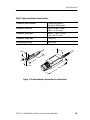
1
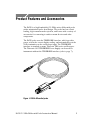
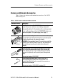
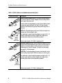
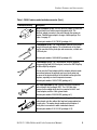
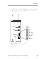
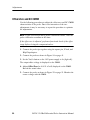
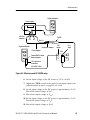
Instruction Manual
P6330
3.5 GHz Differential Probe
071-0757-04
Warning
The servicing instructions are for use by qualified
personnel only. To avoid personal injury, do not
perform any servicing unless you are qualified to
do so. Refer to all safety summaries prior to
performing service.
www.tektronix.com
Copyright © Tektronix, Inc. All rights reserved.
Tektronix products are covered by U.S. and foreign patents, issued and
pending. Information in this publication supercedes that in all previously
published material. Specifications and price change privileges reserved.
Tektronix, Inc., P.O. Box 500, Beaverton, OR 97077
TEKTRONIX, TEK, TEKPROBE, and SureFoot are registered trademarks of
Tektronix, Inc. KlipChip is a trademark of Tektronix, Inc.
WARRANTY
Tektronix warrants that the products that it manufactures and sells will be free from defects
in materials and workmanship for a period of one (1) year from the date of shipment. If a
product proves defective during this warranty period, Tektronix, at its option, either will
repair the defective product without charge for parts and labor, or will provide a
replacement in exchange for the defective product.
In order to obtain service under this warranty, Customer must notify Tektronix of the
defect before the expiration of the warranty period and make suitable arrangements for the
performance of service. Customer shall be responsible for packaging and shipping the
defective product to the service center designated by Tektronix, with shipping charges
prepaid. Tektronix shall pay for the return of the product to Customer if the shipment is to
a location within the country in which the Tektronix service center is located. Customer
shall be responsible for paying all shipping charges, duties, taxes, and any other charges for
products returned to any other locations.
This warranty shall not apply to any defect, failure or damage caused by improper use or
improper or inadequate maintenance and care. Tektronix shall not be obligated to furnish
service under this warranty a) to repair damage resulting from attempts by personnel other
than Tektronix representatives to install, repair or service the product; b) to repair damage
resulting from improper use or connection to incompatible equipment; c) to repair any
damage or malfunction caused by the use of non-Tektronix supplies; or d) to service a
product that has been modified or integrated with other products when the effect of such
modification or integration increases the time or difficulty of servicing the product.
THIS WARRANTY IS GIVEN BY TEKTRONIX IN LIEU OF ANY OTHER
WARRANTIES, EXPRESS OR IMPLIED. TEKTRONIX AND ITS VENDORS
DISCLAIM ANY IMPLIED WARRANTIES OF MERCHANTABILITY OR
FITNESS FOR A PARTICULAR PURPOSE. TEKTRONIX’ RESPONSIBILITY
TO REPAIR OR REPLACE DEFECTIVE PRODUCTS IS THE SOLE AND
EXCLUSIVE REMEDY PROVIDED TO THE CUSTOMER FOR BREACH OF
THIS WARRANTY. TEKTRONIX AND ITS VENDORS WILL NOT BE LIABLE
FOR ANY INDIRECT, SPECIAL, INCIDENTAL, OR CONSEQUENTIAL
DAMAGES IRRESPECTIVE OF WHETHER TEKTRONIX OR THE VENDOR
HAS ADVANCE NOTICE OF THE POSSIBILITY OF SUCH DAMAGES.
Table of Contents
General Safety Summary . . . . . . . . . . . . . . . . . . . . . . . . . . . . . .
Service Safety Summary . . . . . . . . . . . . . . . . . . . . . . . . . . . . . .
Contacting Tektronix . . . . . . . . . . . . . . . . . . . . . . . . . . . . . . . . .
v
vii
viii
Product Features and Accessories . . . . . . . . . . . . . . . . . . . . .
Options . . . . . . . . . . . . . . . . . . . . . . . . . . . . . . . . . . . . . . . . . . . .
Features and Standard Accessories . . . . . . . . . . . . . . . . . . . . . .
Optional Accessories . . . . . . . . . . . . . . . . . . . . . . . . . . . . . . . . .
1
2
3
7
Operating Basics . . . . . . . . . . . . . . . . . . . . . . . . . . . . . . . . . . .
Installation . . . . . . . . . . . . . . . . . . . . . . . . . . . . . . . . . . . . . . . . .
Instruments with the TEKPROBE Interface (Tektronix TDS 400,
500, 600, and 700 Series Oscilloscopes) . . . . . . . . . . . . . . .
Instruments without the TEKPROBE Interface . . . . . . . . . . . .
Input Voltage Limits . . . . . . . . . . . . . . . . . . . . . . . . . . . . . . . . .
Maximum Input Voltage . . . . . . . . . . . . . . . . . . . . . . . . . . . . . .
Common-Mode Signal Range . . . . . . . . . . . . . . . . . . . . . . . . . .
Differential-Mode Signal Range . . . . . . . . . . . . . . . . . . . . . . . .
Common-Mode Rejection . . . . . . . . . . . . . . . . . . . . . . . . . . . . .
Probing Techniques to Maximize CMRR . . . . . . . . . . . . . . . . .
Electrical Effects of Accessories . . . . . . . . . . . . . . . . . . . . . . . .
Input Impedance and Probe Loading . . . . . . . . . . . . . . . . . . . . .
Probe Grounding . . . . . . . . . . . . . . . . . . . . . . . . . . . . . . . . . . . .
9
9
10
10
10
11
11
11
11
12
13
14
15
Functional Check . . . . . . . . . . . . . . . . . . . . . . . . . . . . . . . . . . .
17
Reference . . . . . . . . . . . . . . . . . . . . . . . . . . . . . . . . . . . . . . . . .
Problems with Single-Ended Measurements . . . . . . . . . . . . . . .
Differential Measurements . . . . . . . . . . . . . . . . . . . . . . . . . . . .
Common-Mode Rejection Ratio . . . . . . . . . . . . . . . . . . . . . . . .
Assessing CMRR Error . . . . . . . . . . . . . . . . . . . . . . . . . . . . . . .
Input Impedance Effects on CMRR . . . . . . . . . . . . . . . . . . . . .
Extending the Input Leads . . . . . . . . . . . . . . . . . . . . . . . . . . . . .
Extending the Ground Lead . . . . . . . . . . . . . . . . . . . . . . . . . . . .
Extending the Probe Output . . . . . . . . . . . . . . . . . . . . . . . . . . .
Terminating the Probe . . . . . . . . . . . . . . . . . . . . . . . . . . . . . . . .
Effect of Extending the Output Cable . . . . . . . . . . . . . . . . . . . .
Using the Probe with Other Instruments . . . . . . . . . . . . . . . . . .
19
19
19
20
20
21
21
22
22
22
23
23
P6330 3.5 GHz Differential Probe Instruction Manual
i
Table of Contents
ii
Specifications . . . . . . . . . . . . . . . . . . . . . . . . . . . . . . . . . . . . . .
Warranted Characteristics . . . . . . . . . . . . . . . . . . . . . . . . . . . . .
Typical Characteristics . . . . . . . . . . . . . . . . . . . . . . . . . . . . . . .
Nominal Characteristics . . . . . . . . . . . . . . . . . . . . . . . . . . . . . .
25
25
26
30
Theory of Operation . . . . . . . . . . . . . . . . . . . . . . . . . . . . . . . .
Probe Head and Cable Assembly . . . . . . . . . . . . . . . . . . . . . . .
Compensation Box . . . . . . . . . . . . . . . . . . . . . . . . . . . . . . . . . . .
Offset Amplifier . . . . . . . . . . . . . . . . . . . . . . . . . . . . . . . . . . . . .
Probe Identification EEPROM . . . . . . . . . . . . . . . . . . . . . . . . .
TEKPROBE Interface . . . . . . . . . . . . . . . . . . . . . . . . . . . . . . . .
33
34
34
34
34
35
Performance Verification . . . . . . . . . . . . . . . . . . . . . . . . . . . .
Equipment Required . . . . . . . . . . . . . . . . . . . . . . . . . . . . . . . . .
Equipment Setup . . . . . . . . . . . . . . . . . . . . . . . . . . . . . . . . . . . .
Probe Calibration Fixture . . . . . . . . . . . . . . . . . . . . . . . . . . . . .
Using the Probe Calibration Fixture . . . . . . . . . . . . . . . . . . . . .
Output Offset Voltage . . . . . . . . . . . . . . . . . . . . . . . . . . . . . . . .
DC Gain Accuracy . . . . . . . . . . . . . . . . . . . . . . . . . . . . . . . . . . .
Rise Time . . . . . . . . . . . . . . . . . . . . . . . . . . . . . . . . . . . . . . . . . .
37
37
38
39
39
41
41
43
Adjustments . . . . . . . . . . . . . . . . . . . . . . . . . . . . . . . . . . . . . . .
Equipment Required . . . . . . . . . . . . . . . . . . . . . . . . . . . . . . . . .
Removing the Compensation Box Cover . . . . . . . . . . . . . . . . .
Offset Zero and DC CMRR . . . . . . . . . . . . . . . . . . . . . . . . . . . .
Offset Range . . . . . . . . . . . . . . . . . . . . . . . . . . . . . . . . . . . . . . .
Replacing the Compensation Box Cover . . . . . . . . . . . . . . . . .
47
47
48
50
53
54
Maintenance . . . . . . . . . . . . . . . . . . . . . . . . . . . . . . . . . . . . . . .
Replacing TEKPROBE Interface Pins . . . . . . . . . . . . . . . . . . .
Removing and Replacing the TEKPROBE Interface Collar . .
Inspection and Cleaning . . . . . . . . . . . . . . . . . . . . . . . . . . . . . .
Replacement Parts . . . . . . . . . . . . . . . . . . . . . . . . . . . . . . . . . . .
Preparation for Shipment . . . . . . . . . . . . . . . . . . . . . . . . . . . . . .
55
55
56
57
57
57
Replaceable Parts . . . . . . . . . . . . . . . . . . . . . . . . . . . . . . . . . . .
Parts Ordering Information . . . . . . . . . . . . . . . . . . . . . . . . . . . .
Using the Replaceable Parts List . . . . . . . . . . . . . . . . . . . . . . . .
Item Names . . . . . . . . . . . . . . . . . . . . . . . . . . . . . . . . . . . . . . . .
Indentation System . . . . . . . . . . . . . . . . . . . . . . . . . . . . . . . . . .
Abbreviations . . . . . . . . . . . . . . . . . . . . . . . . . . . . . . . . . . . . . . .
59
59
60
60
60
60
P6330 3.5 GHz Differential Probe Instruction Manual
Table of Contents
List of Figures
Figure 1: P6330 differential probe . . . . . . . . . . . . . . . . . . . . . .
Figure 2: Input connector of TEKPROBE interface . . . . . . . . .
Figure 3: Using the variable spacing adapter . . . . . . . . . . . . . .
Figure 4: Using the TwinFoot adapter . . . . . . . . . . . . . . . . . . . .
Figure 5: Typical effects on a signal using probe tip adapters .
Figure 6: Typical probe input model . . . . . . . . . . . . . . . . . . . . .
Figure 7: Probe ground input . . . . . . . . . . . . . . . . . . . . . . . . . . .
Figure 8: Probe functional check connections . . . . . . . . . . . . .
Figure 9: Simplified model of a differential amplifier . . . . . . .
Figure 10: Twisting the input leads . . . . . . . . . . . . . . . . . . . . . .
Figure 11: Typical common-mode gain . . . . . . . . . . . . . . . . . . .
Figure 12: Typical differential input impedance vs frequency .
Figure 13: Probe head and compensation box dimensions . . . .
Figure 14: Simplified schematic diagram . . . . . . . . . . . . . . . . .
Figure 15: TEKPROBE interface . . . . . . . . . . . . . . . . . . . . . . .
Figure 16: Probe Calibration Fixture . . . . . . . . . . . . . . . . . . . . .
Figure 17: Probe Calibration Fixture test points . . . . . . . . . . . .
Figure 18: Setup for the output offset voltage test . . . . . . . . . .
Figure 19: DC Gain Accuracy setup . . . . . . . . . . . . . . . . . . . . .
Figure 20: Test system rise time setup . . . . . . . . . . . . . . . . . . .
Figure 21: Test system rise time setup with probe . . . . . . . . . .
Figure 22: Verifying both probe pins are contacting the
DM test points . . . . . . . . . . . . . . . . . . . . . . . . . . . . . . . . . . .
Figure 23: Removing the compensation box cover . . . . . . . . . .
Figure 24: Adjustment and test point locations . . . . . . . . . . . . .
Figure 25: Offset zero and DC CMRR setup . . . . . . . . . . . . . .
Figure 26: P6330 offset range setup . . . . . . . . . . . . . . . . . . . . .
Figure 27: Replacing the compensation box cover . . . . . . . . . .
Figure 28: Replacing TEKPROBE interface pins . . . . . . . . . . .
Figure 29: Replacing the TEKPROBE interface collar . . . . . .
Figure 30: P6330 replaceable parts . . . . . . . . . . . . . . . . . . . . . .
Figure 31: P6330 standard accessories . . . . . . . . . . . . . . . . . . .
Figure 32: P6330 optional accessories . . . . . . . . . . . . . . . . . . .
P6330 3.5 GHz Differential Probe Instruction Manual
1
10
12
12
13
14
15
17
20
22
28
28
29
33
35
39
40
41
42
43
44
45
48
49
51
53
54
55
56
61
63
65
iii
Table of Contents
iv
P6330 3.5 GHz Differential Probe Instruction Manual
General Safety Summary
Review the following safety precautions to avoid injury and prevent
damage to this product or any products connected to it. To avoid
potential hazards, use this product only as specified.
To Avoid Fire or Personal Injury
Connect and Disconnect Properly. Connect the probe output to the
measurement instrument before connecting the probe to the circuit
under test. Disconnect the probe input and the probe ground from the
circuit under test before disconnecting the probe from the measurement instrument.
Observe All Terminal Ratings. To avoid fire or shock hazard, observe all
ratings and markings on the product. Consult the product manual for
further ratings information before making connections to the product.
The common terminal is at ground potential. Do not connect the
common terminal to elevated voltages.
Do Not Operate Without Covers. Do not operate this product with
covers or panels removed.
Do Not Operate With Suspected Failures. If you suspect there is damage
to this product, have it inspected by qualified service personnel.
Do Not Operate in Wet/Damp Conditions.
Do Not Operate in an Explosive Atmosphere.
Keep Product Surfaces Clean and Dry.
P6330 3.5 GHz Differential Probe Instruction Manual
v
General Safety Summary
Safety Terms and Symbols
Terms in This Manual. These terms may appear in this manual:
WARNING. Warning statements identify conditions or practices that
could result in injury or loss of life.
CAUTION. Caution statements identify conditions or practices that
could result in damage to this product or other property.
Terms on the Product. These terms may appear on the product:
DANGER indicates an injury hazard immediately accessible as you
read the marking.
WARNING indicates an injury hazard not immediately accessible as
you read the marking.
CAUTION indicates a hazard to property including the product.
Symbols on the Product. These symbols may appear on the product:
CAUTION
Refer to Manual
vi
P6330 3.5 GHz Differential Probe Instruction Manual
Service Safety Summary
Only qualified personnel should perform service procedures. Read
this Service Safety Summary and the General Safety Summary before
performing any service procedures.
Do Not Service Alone. Do not perform internal service or adjustments
of this product unless another person capable of rendering first aid
and resuscitation is present.
P6330 3.5 GHz Differential Probe Instruction Manual
vii
Service Safety Summary
Contacting Tektronix
Phone
1-800-833-9200*
Address
Tektronix, Inc.
Department or name (if known)
14200 SW Karl Braun Drive
P.O. Box 500
Beaverton, OR 97077
USA
Web site
www.tektronix.com
Sales
support
1-800-833-9200, select option 1*
Service sup- 1-800-833-9200, select option 2*
port
Technical
support
Email: [email protected]
1-800-833-9200, select option 3*
6:00 a.m. - 5:00 p.m. Pacific time
*
viii
This phone number is toll free in North America. After office
hours, please leave a voice mail message.
Outside North America, contact a Tektronix sales office or
distributor; see the Tektronix web site for a list of offices.
P6330 3.5 GHz Differential Probe Instruction Manual
Product Features and Accessories
The P6330 is a high-bandwidth (3.5 GHz) active differential probe
with a miniaturized probe head design. The probe has low circuit
loading, high common-mode rejection, and comes with a variety of
accessories for connecting to surface-mount devices and other
components.
The P6330 probe uses the TEKPROBE interface, which provides
power, selects the correct display scaling, and automatically sets the
50 Ω termination on the oscilloscope input. The TEKPROBE
interface is standard on many Tektronix TDS series oscilloscopes.
The Tektronix 1103 TEKPROBE Power Supply can be used for
instruments without the TEKPROBE interface (refer to page 7).
Figure 1: P6330 differential probe
P6330 3.5 GHz Differential Probe Instruction Manual
1
Product Features and Accessories
Options
The following options are available when ordering the P6330 probe:
H Option D1 - Calibration Data
H Option C3 - 3 years Calibration Service
H Option D3 - 3 years Calibration Data (requires Option C3)
H Option R3 - 3 years Extended Warranty
2
P6330 3.5 GHz Differential Probe Instruction Manual
Product Features and Accessories
Features and Standard Accessories
Table 1 shows the features and standard accessories of the P6330
differential probe.
Table 1: P6330 features and standard accessories
Feature/Accessory
Description
TEKPROBE interface. The TEKPROBE interface supplies
power to the probe, selects the correct display scaling, and
automatically sets the 50 Ω termination on the oscilloscope input.
If your oscilloscope does not have the TEKPROBE interface, you
can use the optional 1103 power supply (refer to page 7).
Input connections. The plus and minus connections of the probe
head accept the standard and optional probe accessories (some
of which connect through the square pin adapter).
+
-
Ground
WARNING: Skin penetration hazard. To prevent injury, install the
probe tip cover when the probe is not in use. The probe tips are
extremely sharp to ensure good contact and measurement
integrity.
Probe tip cover. The probe tips are extremely sharp to ensure
good contact and measurement integrity. When not using the
probe, slide the probe tip cover over the probe head to prevent
damage to the probe tips and to protect yourself from personal
injury.
Tektronix part number: 200-4236-00
Three-inch ground lead (2 ea). Use the ground lead for
connecting the probe ground to the circuit, if needed. The
socketed end of the lead may be connected to accessories, or
fitted onto 0.025-inch pins.
Tektronix part number: 196-3469-00 (package of 2)
P6330 3.5 GHz Differential Probe Instruction Manual
3
Product Features and Accessories
Table 1: P6330 features and standard accessories (Cont.)
Feature/Accessory
Description
Variable spacing adapter (4 ea). The variable spacing adapter
fits over the probe tip. Push the adapter onto the probe tip until it
seats against the probe head.
Use the variable spacing adapter to probe any two adjacent leads
or test points spaced between 0.020 and 0.180-inches apart.
Adjust the articulated pins by gently rotating them using a pair of
tweezers.
NOTE: The articulated pins can be bent, but they are fragile. Use
extreme care when bending the pins.
Seated
against
probe head
The elastomeric contacts inside the adapter are rated for 50 -- 75
insertion cycles with the probe tip. Replace the adapter after
exceeding these limits to avoid unreliable operation.
Tektronix part number: 016-1885-00 (package of 4)
Square pin adapter (4 ea). Push the square pin adapter onto the
probe tip until it seats against the probe head. Use the square pin
adapter to connect the probe to other accessories, such as the
Y-lead adapter or TwinFoot adapter. The inputs on the adapter
are spaced 0.100-inches apart.
CAUTION: To avoid damaging the square pin connectors, do not
insert anything larger than a 0.025-inch square pin into the inputs.
The elastomeric contacts inside the adapter are rated for 50 -- 75
insertion cycles with the probe tip. Replace the adapter after
exceeding these limits to avoid unreliable operation.
Seated
against
probe head
Tektronix part number: 016-1884-00 (package of 4)
4
P6330 3.5 GHz Differential Probe Instruction Manual
Product Features and Accessories
Table 1: P6330 features and standard accessories (Cont.)
Feature/Accessory
Description
TwinFoot adapter (4 ea). Use the TwinFoot adapter to probe two
adjacent leads on a surface-mount integrated circuit. The
TwinFoot adapter connects to the probe through the square pin
adapter. Flexible fingers adapt to a range of lead spacings. See
Figure 4 on page 12.
Tektronix part number: 016-1785-00 (package of 4)
Y-lead adapter (2 ea). The Y-lead adapter connects to the probe
through the square pin adapter. The socketed ends of the leads
may be connected to the probe tips and accessories, or fitted onto
0.025-inch pins.
Tektronix part number: 196-3468-00 (package of 2)
X-lead adapter (2 ea). The X-lead adapter connects between
accessories fitted with 0.025-inch pins, such as the SMT KlipChip
and Micro KlipChip adapters.
You can use the X-lead adapter with the adapters below to make
connections between the probe tip and your circuit under test.
Be aware of the electrical effects of the added lead length of the
adapters, especially as circuit frequencies increase.
Tektronix part number: 196-3473-XX (package of 1)
SMT KlipChip adapter (2 ea). Use this accessory to probe the
leads on dual-in-line packages (DIP). The 0.025-inch pins
recessed in the adapter body may be connected to the X- and
Y-lead adapters, and the 3-inch ground leads.
Tektronix part number: 206-0364-XX (package of 1)
Color marker bands
Color marker bands (10 ea). Attach matching pairs of the color
marker bands onto the cable at the head and compensation box
of each probe. The marker bands enable quick verification of
which probe is connected to which instrument channel.
Tektronix part number: 016-1315-00 (package of 10)
P6330 3.5 GHz Differential Probe Instruction Manual
5
Product Features and Accessories
Table 1: P6330 features and standard accessories (Cont.)
Feature/Accessory
Description
Plastic accessory box. Use the plastic box to store the probe
accessories when not in use.
Tektronix part number: 006-7164-00
Instrument case. The instrument case protects the probe from
harsh environments and provides room for storing optional
accessories.
Tektronix part number: 016-1879-XX
Calibration certificate. A certificate of traceable calibration is
provided with every instrument shipped.
Instruction Manual. Provides instructions for operating the
P6330 differential probe and procedures for verifying the
performance, adjusting, and maintaining the probe.
Tektronix part number: 071-0757-XX
Accessory reorder sheet.
The accessory reorder sheet provides photos and part numbers
for identifying standard and optional accessories that are
compatible with your probe.
Tektronix part number 001-1362-XX
Antistatic wrist strap. When using the probe, always work at an
antistatic work station and wear the antistatic wrist strap.
Tektronix part number: 006-3415-04
6
P6330 3.5 GHz Differential Probe Instruction Manual
Product Features and Accessories
Optional Accessories
Table 2 shows the optional accessories that you can order for the
P6330 differential probe.
Table 2: Optional accessories
Accessory
Description
Release tool. Use for opening the compensation box to access
adjustments.
Order Tektronix part number 003-1383-00
Adjustment tool. Use for making internal adjustments to the
probe.
Order Tektronix part number 003-0675-01
Probe calibration fixture. Use the probe calibration fixture to
perform some of the calibration procedures. The calibration fixture
connects to signal sources used to test the probe characteristics.
Refer to page 39 for details on using the fixture.
Order Tektronix part number 067-0419-XX
1103 Power supply. Order the 1103 power supply for
performance verification procedures, and for instruments that do
not have the TEKPROBE Interface. Power cord options are
available for the following countries or regions.
Standard. North America and Japan
Option A1. European
Option A2. UK
Option A3. Australia
Option A5. Switzerland
P6330 3.5 GHz Differential Probe Instruction Manual
7
Product Features and Accessories
Table 2: Optional accessories (Cont.)
Accessory
Description
50 Ω termination. Terminates the output of the 1103 power
supply to the required 50 Ω if the oscilloscope does not have a
50 Ω input setting. Order Tektronix part number 011-0049-01.
50 Ω BNC cable. Connects to the 1103 output.
Order Tektronix part number: 012-0076-00
IEEE1394 Adapter. The IEEE1394 Adapter allows you to probe
signals on the bus, external to system enclosures, without
disturbing system operation. The adapter maintains a balanced
55 Ω signal path and can be used in both single-ended and
differential modes.
Order Tektronix part number: 679-5027-00
Micro KlipChip adapters (2 ea). Use the adapters to probe the
leads on integrated circuits that are surface-mounted. The
0.025-inch pin at the back of the adapter may be connected to the
X- and Y-lead adapters, and the 3-inch ground leads.
Order Tektronix part number: SMK4 (package of 4)
8
P6330 3.5 GHz Differential Probe Instruction Manual
Operating Basics
This section discusses operating considerations and probing
techniques. For more detailed information about differential
measurements and common-mode rejection ratio (CMRR), see the
Reference section on page 19.
The P6330 probe design is optimized for high bandwidth, low
capacitance applications; it is not a general purpose probe. The probe
head and tips are miniaturized for electrical characteristics and
access to dense circuitry, and must be handled carefully. Rough or
careless use will likely damage the probe.
To avoid damaging the probe tips, minimize your lateral pressure on
the tips. Always probe as directly straight onto the circuit (perpendicular) as possible. The probe tips are extremely sharp to ensure good
contact and measurement integrity.
WARNING. Skin penetration hazard. Use care when handling the
probe. To prevent injury and/or probe damage, install the protective
cover over the probe tips when the probe is not in use.
Installation
Before you connect the output of the P6330 differential probe,
determine whether or not your oscilloscope has a TEKPROBE
interface. See Figure 2 on page 10.
P6330 3.5 GHz Differential Probe Instruction Manual
9
Operating Basics
Figure 2: Input connector of TEKPROBE interface
Instruments with the TEKPROBE Interface (Tektronix TDS 400, 500, 600,
and 700 Series Oscilloscopes)
On instruments that have the TEKPROBE interface, simply connect
the probe to the input. The TEKPROBE interface provides power,
selects the correct display scaling, and automatically sets the 50 Ω
termination on the oscilloscope input.
NOTE. TDS 400 and TDS 400A series oscilloscopes do not interpret
the scale factor coding of the P6330 differential probe. To correct for
this problem, divide the measurement (or scale factor) by 5.
Instruments without the TEKPROBE Interface
On instruments that do not have the TEKPROBE interface, you must
order the optional 1103 power supply (refer to page 7). Each 1103
can supply power for two probes. The input of the oscilloscope must
also terminate into 50 Ω. Refer to page 22 for information on the
effects of extending the output of the probe.
Input Voltage Limits
The P6330 differential probe is designed to probe low-voltage
circuits. Before probing a voltage, take into account the limits for
maximum input voltage, the common-mode signal range, and the
differential-mode signal range. For specific limits, see Specifications
on page 25.
10
P6330 3.5 GHz Differential Probe Instruction Manual
Operating Basics
Maximum Input Voltage
The maximum input voltage is the maximum voltage to ground that
the inputs can withstand without damaging the input circuitry of the
probe.
CAUTION. To avoid damaging the inputs of the P6330 differential
probe, do not apply more than ± 15 V (DC + peak AC) between each
input and ground.
Common-Mode Signal Range
The common-mode signal range is the maximum voltage that you
can apply to each input, with respect to earth ground, without
saturating the input circuitry of the probe. A common-mode voltage
that exceeds the common-mode signal range may produce an
erroneous output waveform even when the differential-mode
specification is met. For Specifications, refer to page 25.
Differential-Mode Signal Range
The differential-mode signal range is the maximum voltage
difference between the plus and minus inputs that the probe can
accept without distorting the signal. The distortion from a voltage
that is too large can result in a clipped or otherwise distorted and
inaccurate measurement. For Specifications, refer to page 25.
Common-Mode Rejection
The common-mode rejection ratio (CMRR) is the ability of a probe
to reject signals that are common to both inputs. More precisely,
CMRR is the ratio of the differential gain to the common-mode gain.
The higher the ratio, the greater the ability to reject common-mode
signals.
Common-mode rejection decreases as the input frequency increases.
Figure 11 on page 28 is a plot of typical CMRR of the probe versus
input frequency. For additional information about CMRR, see
page 20.
P6330 3.5 GHz Differential Probe Instruction Manual
11
Operating Basics
Probing Techniques to Maximize CMRR
The common-mode rejection of the probe is highest when the probe
is applied directly to the circuit, without using adapters. However,
some probing tasks are made easier using accessories included with
the probe. The accessories shown in Figures 3 and 4 achieve a high
CMRR by minimizing the distance between the probe head and the
signal source.
Figure 3: Using the variable spacing adapter
IC leads being probed
TwinFoot adapter
Square pin adapter
Probe
Conductive side
of probe tip
Insulated side of probe tip
Figure 4: Using the TwinFoot adapter
12
P6330 3.5 GHz Differential Probe Instruction Manual
Operating Basics
Electrical Effects of Accessories
The probe tip accessories included with your probe help connect to
different types of components. While these accessories make
connections easier, be aware that the adapter you choose may affect
the signal you are measuring, depending on a variety of factors,
including signal frequency, source impedance, and lead length.
Use the probe only (without adapters) to optimize step and frequency
response. Using the probe tip adapters adds inductance and
capacitance, which increases step response and aberrations, and leads
to increased ripples in frequency response. These effects increase as
the source impedance and the measured waveform risetimes
decrease.
The recommended method for hands-free probing is to use the probe
only (without adapters), with a probe positioner such as a Tektronix
PPM203B. If you need a tip space between 0.020 and 0.180 inches
apart, use the variable spacing adapter and the probe positioner. Use
the square pin adapter for test points or component leads spaced
farther than 0.180 inches apart.
Figure 5 illustrates the typical effects on a given signal using some of
the adapters included with your probe.
Probe only
Variable
spacing
adapter
Square pin
adapter
Figure 5: Typical effects on a signal using probe tip adapters
P6330 3.5 GHz Differential Probe Instruction Manual
13
Operating Basics
Input Impedance and Probe Loading
When you connect the probe inputs to a circuit, you are introducing a
new resistance, capacitance, and inductance into the circuit. Each
input of the P6330 differential probe has a characteristic input
impedance of 50 kΩ to ground in parallel with less than 0.4 pF. See
Figure 6.
For signals with low source impedance and frequency, the 50 kΩ
input impedance on each input is large enough to prevent the inputs
from loading the signal sources. The greater the source impedances
and the higher the signal frequencies, the more you must take these
factors into account.
+ Input
0.4 pF
50 kΩ
Ground
0.4 pF
0.1 pF
50 kΩ
- Input
Figure 6: Typical probe input model
As the impedance of the signal source on an input increases, the
more the probe loads the source and reduces the signal amplitude.
The frequency of the signal also affects signal measurement. As the
frequency of the signal increases, the input impedance of the probe
decreases. The lower the impedance of the probe relative to that of
the source, the more the probe loads the circuit under test and
reduces the signal amplitude. For a graph of frequency versus input
impedance, refer to Figure 12 on page 28.
14
P6330 3.5 GHz Differential Probe Instruction Manual
Operating Basics
Probe Grounding
In addition to the plus and minus inputs on the probe head, there is
also a ground (common) input. The ground lead slides into the notch
on the side of the probe. See Figure 7.
+
Ground
Figure 7: Probe ground input
CAUTION. To avoid damaging the circuitry under test, connect the
probe ground (common), if used, to a ground-reference point only.
In most applications, the common-mode impedance to ground is
greater than the differential impedance. Adding the probe ground
lead does not improve the high-frequency performance of the
measurement. You can use the probe to take a differential measurement regardless of whether or not the ground (common) is connected.
There are some applications that may require a ground reference
connection to maintain measurement accuracy. Generally this is
necessary when probing circuits which are fully isolated from
ground, such as battery operated devices.
P6330 3.5 GHz Differential Probe Instruction Manual
15
Operating Basics
16
P6330 3.5 GHz Differential Probe Instruction Manual
Functional Check
After installing the probe on the oscilloscope, a functional check
may be performed using the PROBE COMPENSATION connections
on the front panel of the oscilloscope. See Figure 8.
Figure 8: Probe functional check connections
1. Connect the probe to the oscilloscope.
2. Set the oscilloscope to display the probe channel.
3. Connect the square pin adapter to the probe tip, and connect the
Y-lead adapter to the square pin adapter. Plug the SMT KlipChips
into the Y-lead adapter.
4. Connect the SMT KlipChips to the PROBE COMPENSATION
connections on the oscilloscope.
5. Adjust the oscilloscope to display a stable calibration waveform.
P6330 3.5 GHz Differential Probe Instruction Manual
17
Functional Check
NOTE. If your instrument supports probe calibration routines, now is
a good time to perform them.
6. Disconnect the probe from the PROBE COMPENSATION
connector and connect the two KlipChips together.
7. With the probe offset set to 0.0 V, the oscilloscope display should
be at the ground reference.
8. Set the oscilloscope volts/division to 500 mV.
9. Adjust the probe offset. The displayed waveform should vary
between approximately +1.0 V and - 1.0 V.
18
P6330 3.5 GHz Differential Probe Instruction Manual
Reference
This section contains important reference information about
differential measurements and how to increase the accuracy of your
measurements.
Problems with Single-Ended Measurements
While suitable in many applications, single-ended measurements can
present problems in the following situations:
H When the signal is not referenced to earth ground
H When the signal being measured is distorted or changed by
connecting or disconnecting the probe ground reference lead
Differential Measurements
Devices designed to make differential measurements avoid the
problems posed by single-ended systems. These devices include a
variety of differential probes, differential amplifiers, and isolators.
The differential amplifier (Figure 9) is at the heart of any device or
system designed to make differential measurements. Ideally, the
differential amplifier rejects any voltage that is common to the inputs
and amplifies any difference between the inputs. Voltage that is
common to both inputs is often referred to as the Common-Mode
Voltage (VCM) and voltage that is different as the Differential-Mode
Voltage (VDM).
P6330 3.5 GHz Differential Probe Instruction Manual
19
Reference
+
Vout
+
-
Differential
mode VDM
+
Common
V
mode CM
Figure 9: Simplified model of a differential amplifier
Common-Mode Rejection Ratio
In reality, differential amplifiers cannot reject all of the commonmode signal. The ability of a differential amplifier to reject the
common-mode signal is expressed as the Common-Mode Rejection
Ratio (CMRR). The CMRR is the differential-mode gain (ADM)
divided by the common-mode gain (ACM). It is expressed either as a
ratio or in dB.
CMRR =
A DM
dB = 20 log
A CM
A DM
A CM
CMRR generally is highest (best) at DC and degrades with
increasing frequency.
Assessing CMRR Error
Figure 11 on page 28 shows the CMRR of the P6330 differential
probe. This derating chart assumes a common-mode signal that is
sinusoidal.
20
P6330 3.5 GHz Differential Probe Instruction Manual
Reference
A quick way to assess the magnitude of CMRR error when the
common-mode signal is not sinusoidal is to connect both leads to the
same point in the circuit. The oscilloscope will display only the
common-mode component which is not fully rejected by the probe.
While this technique may not give you entirely accurate measurements, it does allow you to determine if the magnitude of the
common-mode error signal is significant.
Input Impedance Effects on CMRR
The lower the input impedance of the probe relative to the source
impedance, the lower the CMRR. See Figure 12 on page 28.
Significant differences in the source impedance driving the two
inputs will also lower the CMRR.
Extending the Input Leads
At times it may be necessary to extend the probe inputs with wires or
a probe tip adapter. When you do this, you should minimize the lead
lengths to optimize common-mode rejection and twist the input leads
together as shown in Figure 10.
Twisting the input leads together does increase capacitance that may
degrade high-frequency performance. You should take into account
any effects caused by the extended leads when you take a measurement.
P6330 3.5 GHz Differential Probe Instruction Manual
21
Reference
Square pin
adapter
Figure 10: Twisting the input leads
Extending the Ground Lead
Extending the ground lead will have little, if any, affect on your
measurements. In most circuits, the ground path from the differential
source has sufficiently high impedance to damp out any ringing
caused by lead inductance.
Extending the Probe Output
With the 1103 TEKPROBE power supply, it is possible to extend the
output of the probe to connect the probe to other types of measurement instruments or to connect the probe to a signal source that is
outside the reach of the probe.
Terminating the Probe
The probe must terminate into 50 Ω at the input of the measurement
instrument. Use the 1103 TEKPROBE power supply to adapt the
differential probe and set the input impedance of the measurement
instrument to 50 Ω. If the measurement instrument does not support
50 Ω input termination, connect a 50 Ω coaxial terminator on the
input.
22
P6330 3.5 GHz Differential Probe Instruction Manual
Reference
Effect of Extending the Output Cable
As the frequency of a signal increases, current flow concentrates at
the outer edges of the conductor, effectively increasing the
impedance. This effect is known as skin loss. The P6330 probe
contains circuitry to compensate for skin loss.
The compensation provides flat response with the probe cable.
Extending the length of the output cable increases the amount of skin
loss beyond the range of compensation correction. Minimizing the
length of cable extension reduces the attenuation.
In critical applications which require high amplitude accuracy, you
should first characterize the response of the probe with the extension
using a leveled sinewave generator and power meter. Then, you can
factor the characterization results into the measurement.
Using the Probe with Other Instruments
You can use the P6330 differential probe with other types of
measurement instruments, such as spectrum analyzers, time internal
analyzers, and network analyzers.
When using the differential probes with these instruments, you must
use the 1103 TEKPROBE power supply, and normalize the probe
with the instrument before making a measurement.
P6330 3.5 GHz Differential Probe Instruction Manual
23
Reference
24
P6330 3.5 GHz Differential Probe Instruction Manual
Specifications
The specifications in Tables 3 through 6 apply to a P6330 probe
installed on a TDS8000 oscilloscope. When the probe is used with
another oscilloscope, the oscilloscope must have an input impedance
of 50 Ω. The probe must have a warm-up period of at least
20 minutes and be in an environment that does not exceed the limits
described in Table 3. Specifications for the P6330 differential probe
fall into three categories: warranted, typical, and nominal characteristics.
Warranted Characteristics
Warranted characteristics (Table 3) describe guaranteed performance
within tolerance limits or certain type-tested requirements.
Warranted characteristics that have checks in the Performance
Verification section are marked with the n symbol.
Table 3: Warranted electrical characteristics
Characteristic
Description
n DC gain
0.2 ± 2%
n Output offset voltage
± 10 mV (+ 20_ C to + 30_ C,
+ 68_ F to + 86_ F)
± 50 mV displayed on screen with
TEKPROBE interface
n Rise time (probe only)
140 ps (130 ps typical)
Maximum nondestructive input voltage
± 15 V(DC + peak AC) between signal and
common of the same channel.
Delay variation (probe-to-probe)
600 ps maximum
Temperature
Operating: 0 to + 40_ C
(+ 32 to + 104_ F)
Nonoperating: -- 55 to + 75_ C
(--131 to + 167_ F)1
P6330 3.5 GHz Differential Probe Instruction Manual
25
Specifications
Table 3: Warranted electrical characteristics (Cont.)
Characteristic
Description
Humidity
Operating: 0--90% RH, tested at
+ 30 to + 40_ C (+ 68 to + 104_ F)
Nonoperating: 0--90% RH, tested at
+ 30 to + 60_ C (+ 68 to + 140_ F)
1
See warning that follows.
WARNING. To avoid a burn hazard at high ambient temperatures, do
not touch the probe with bare hands at nonoperating temperatures
above + 70_ C. Allow sufficient time for the probe to cool before
handling.
Typical Characteristics
Typical characteristics (Tables 4 and 5) describe typical but not
guaranteed performance.
Table 4: Typical electrical characteristics
Characteristic
Description
Bandwidth (probe only)
DC to ≥ 3.5 GHz (-- 3dB)
Differential signal range
± 2.0 V
Differential offset range
±1V
Linearity
± 1% or less of dynamic range
Common-mode signal range
+ 5 V to --4 V
Common-mode rejection ratio
≥60 dB at DC
≥55 dB at 1 MHz
≥45 dB at 30 MHz
≥25 dB at 1 GHz
26
P6330 3.5 GHz Differential Probe Instruction Manual
Specifications
Table 4: Typical electrical characteristics (Cont.)
Characteristic
Description
Delay time
5.4 ns
Differential input resistance, DC coupled
100 kΩ ± 2%
Differential input capacitance
< 0.3 pF at 100 MHz
Common-mode input resistance, DC
coupled
50 kΩ ± 2% (per side)
Common-mode input capacitance
< 0.45 pF at 100 MHz (per side)
Input impedance
See Figure 12
Noise, referred to input
35 nV/√Hz
DC Offset Scale Accuracy
(gain of offset signal path)
ᐔ2.0%
DC Offset Drift
150 V/°C or less at output of probe
0.75 mV/°C or less displayed on screen with
TEKPROBE interface
DC Voltage Measurement Accuracy
(referred to input)
ᐔ[2% of input + (2% of offset) + 50.0 mV +
40.0 mV]
gain error = ᐔ2% of input voltage
offset gain error =ᐔ2% of effective offset at
probe tip
output zero = ᐔ50 mV effective at probe tip
linearity error = ᐔ1.0% of 4.0 V dynamic
range (40.0 mV)
P6330 3.5 GHz Differential Probe Instruction Manual
27
Specifications
Figure 11 shows the typical common-mode gain of the probe. The
CMRR can be approximated by subtracting the common-mode gain
from the - 14 dB reference level. For example, - 80 dB CM gain
equals +66 dB CMRR.
- 44
Gain dB
- 52
- 60
- 68
- 76
- 84
1 MHz
10 MHz
100 MHz
1 GHz
Frequency
Figure 11: Typical common-mode gain
The graph in Figure 12 represents simulation results of a first order
model of the probe input.
Impedance (Ω)
100 k
10 k
1k
100
10
1M
10 M
100 M
Frequency (Hz)
1G
Figure 12: Typical differential input impedance vs frequency
28
P6330 3.5 GHz Differential Probe Instruction Manual
Specifications
Table 5: Typical mechanical characteristics
Dimensions, input connection
2.5 mm (0.99 in) pins on
2.54 mm (0.100 in) centers
Dimensions, control box
82 mm × 28 mm × 23 mm
(3.2 in × 1.1 in × 0.9 in)
Dimensions, probe head
59 mm × 7.7 mm × 5.1 mm
(2.3 in × 0.3 in × 0.2 in)
Dimensions, output cable
1.3 m (51 in)
Unit weight (probe only)
160 g (5.4 oz)
1.1 in
0.3 in
2.3 in
0.9 in
0.2 in
0.1 in
3.2 in
Figure 13: Probe head and compensation box dimensions
P6330 3.5 GHz Differential Probe Instruction Manual
29
Specifications
Nominal Characteristics
Nominal characteristics (Table 6) describe guaranteed traits, but the
traits do not have tolerance limits.
Table 6: Nominal electrical characteristics
Input configuration
Differential (two inputs, + and -- ), with case
ground
Attenuation
5X
Input coupling
DC
Termination
Terminate output into 50 Ω
30
P6330 3.5 GHz Differential Probe Instruction Manual
WARNING
The following servicing instructions are for use only by
qualified personnel. To avoid injury, do not perform any
servicing other than that stated in the operating instructions
unless you are qualified to do so. Refer to all safety
summaries before performing any service.
Theory of Operation
There are no user replaceable parts within the probe or the
compensation box; however, this theory of operation is provided to
assist you in isolating failures to either the probe or the host
oscilloscope. Refer to Figure 14 for a simplified schematic of the
probe.
Probe Head
Compensation Box
Oscilloscope
Probe Tip
IN +
Signal Out
Probe Tip
Ampifier
+ offset
+
in
-
Probe ID Out
Clock In
EEPROM
Offset Ampifier
±1 V Offset
Offset
Zero
- offset
+
Probe Tip
-
Offset
Gain
IN +7 V
Linear
regulator
+15 V
+5 V
-5 V
Ground
Probe
Cable
TEKPROBE
Interface
Figure 14: Simplified schematic diagram
P6330 3.5 GHz Differential Probe Instruction Manual
33
Theory of Operation
Probe Head and Cable Assembly
The probe head assembly contains an active amplifier circuit that
buffers and amplifies the input signal. The amplifier receives power
and an offset level from the compensation box assembly via the
cable assembly.
All signal amplification and buffering is performed in the probe head
assembly. No further amplification takes place in the compensation
box.
Compensation Box
The compensation box contains the following circuits:
H Offset amplifier
H Probe identification EEPROM
H TEKPROBE interface
H DC CMRR adjustment circuitry
H VCC, +7 V linear regulator
Offset Amplifier
The offset amplifier is used to offset the DC component of the input
signal so that it stays at the optimal point of the linear dynamic range
of the probe.
The offset amplifier receives offset information as a ±1 VDC voltage
from the oscilloscope. The amplifier then amplifies it to match the
probe characteristics and applies it to the probe hybrid circuit.
The offset amplifier has two adjustments: offset zero and offset gain.
These adjustments rarely need attention; however, detailed
adjustment instructions are in the Adjustments section on page 47.
Probe Identification EEPROM
The probe identification EEPROM is used to configure the
oscilloscope to the probe. The EEPROM receives a clock input from
the oscilloscope, and information about the probe is passed to the
oscilloscope.
34
P6330 3.5 GHz Differential Probe Instruction Manual
Theory of Operation
TEKPROBE Interface
The TEKPROBE interface provides a communication path between
the probe and the oscilloscope. Contact pins provide power, signal,
offset, and data transfer for the probe identification EEPROM.
Figure 15 shows the TEKPROBE interface pin functions. Refer to
the service documenation for your oscilloscope for more detailed
specifications.
- 15 V
-5 V
Offset
Ground
Signal
Data
Clock
+5 V
+15 V
Figure 15: TEKPROBE interface
P6330 3.5 GHz Differential Probe Instruction Manual
35
Theory of Operation
36
P6330 3.5 GHz Differential Probe Instruction Manual
Performance Verification
Use the following procedures to verify specifications of the P6330
probe. Before beginning these procedures, refer to page 46 and
photocopy the test record, and use it to record the performance test
results. The recommended calibration interval is one year.
These procedures test the following specifications:
H Output offset voltage
H DC gain accuracy
H Rise time
Equipment Required
Refer to Table 7 for a list of the equipment required to verify the
performance of your probe.
Table 7: Equipment required for performance verification
Item description
Performance requirement
Recommended example
High Speed Sampling
Oscilloscope
10 GHz bandwidth
Tektronix TDS8000 with
80E04 module or 11800 with
SD24 module
Probe Calibration Fixture
See page 39
067-0419-00
Probe Positioner
Tektronix PPM203B
Power Supply
TEKPROBE interface
Tektronix 1103
Power Supply
5.0 VDC at 1 mA
Tektronix PS280
DMM (2), with leads
0.1 mV resolution
Fluke 87 or equivalent
Feedthrough Termination
BNC, 50 Ω ±0.05 Ω
011-0129-00
Coaxial cables (2)
Male-to-Male SMA, 20 in
174-1427-00
Coaxial cable
Male-to-Male BNC, 50 Ω
012-1342-00
P6330 3.5 GHz Differential Probe Instruction Manual
37
Performance Verification
Table 7: Equipment required for performance verification (Cont.)
Item description
Performance requirement
Recommended example
Precision coaxial cable
Male-to-Male SMA, 1 ns
delay
015-0562-00
Adapter
SMA Female-to-Female
015-1012-00
Adapters (2)
SMA Female-to-BNC Male
015-0572-00
Adapter
SMA Male jack
131-7128-00
Adapter
BNC Female-to-Dual
Banana
103-0090-00
Adapter
Square pin adapter
016-1884-00
Adapter
Y-lead adapter
196-3434-00
Adapters (2)
KlipChip adapter
206-0364-00
Equipment Setup
Use this procedure to set up the equipment to test the probe.
1. Connect the probe to the 1103 power supply.
2. Turn on 1103 power supply.
3. Turn on the oscilloscope.
4. Allow 20 minutes for the equipment to warm up.
38
P6330 3.5 GHz Differential Probe Instruction Manual
Performance Verification
Probe Calibration Fixture
Some of the procedures in this manual use a probe calibration
fixture, Tektronix part number 067-0419-00.
The calibration fixture provides a means to test the probe for both
common mode and differential mode measurements. SMA
connectors allow stimulus signals to connect to the fixture and are
located on the front and back of the fixture. The fixture is designed
to be used with a probe positioner, such as a Tektronix PPM203B.
Figure 16: Probe Calibration Fixture
Using the Probe Calibration Fixture
1. Connect the fixture to the test circuit using an SMA cable.
2. Connect the 50 Ω terminator included with the fixture to the
unused SMA connector.
3. Insert and secure the probe in a probe positioner.
4. Position the probe over the fixture, using either the positioner
coarse adjustment or otherwise manipulating the positioner arm
in place.
P6330 3.5 GHz Differential Probe Instruction Manual
39
Performance Verification
5. Using the fine position and/or pressure adjust, maneuver the
probe so that the pins contact the CM or DM test points,
depending on which test you are performing. (See Figure 17.)
Common mode
Differential mode
Figure 17: Probe Calibration Fixture test points
6. Verify that contact is made on both pins. (You may need to
readjust the fine position and/or pressure adjustment to make
positive contact with the test points.)
7. Proceed with the specific test instructions.
40
P6330 3.5 GHz Differential Probe Instruction Manual
Performance Verification
Output Offset Voltage
1. Connect the probe as shown in Figure 18.
Digital multimeter
Female BNC-to-male
banana adapter
CH 1
output
1103
50 Ω precision
terminator
KlipChip
adapters
CH 1
input
50 Ω BNC cable
Y-lead
adapter
Square pin
adapter
Figure 18: Setup for the output offset voltage test
2. Set the Var/0v button on the 1103 power supply to 0v (light off).
3. Verify that the output voltage is 0 V, ±10 mV.
DC Gain Accuracy
1. Connect the probe input to the DC source, as shown in Figure 19
on page 42. Monitor the source voltage with the DMM.
2. Set the input voltage on the DC source to approximately +0.5 V.
Record the actual voltage as Vin1.
P6330 3.5 GHz Differential Probe Instruction Manual
41
Performance Verification
Digital multimeter
Power supply
--
+
KlipChip
adapters
P6330
Red (+)
Black (-- )
Digital multimeter
Square pin adapter
Y-lead adapter
CH 1
output
CH 1
input
1103
Female BNC-to-male
banana adapter
50 Ω precision
terminator
50 Ω BNC cable
Figure 19: DC Gain Accuracy setup
3. Record the output voltage as Vout1.
4. Set the input voltage on the DC source to approximately - 0.5 V.
Record the actual voltage as Vin2.
5. Record the output voltage as Vout2.
6. Calculate the gain as follows: (Vout1 - Vout2) ÷ (Vin1 - Vin2).
7. Verify that the gain is 0.2, ± 2%.
42
P6330 3.5 GHz Differential Probe Instruction Manual
Performance Verification
Rise Time
This procedure verifies that the probe meets rise time specifications.
Two rise times are measured; the test system, and the test system
with the probe included. The probe rise time is calculated using the
two measurements.
1. Connect the test equipment as shown in Figure 20.
SD24/ 80E04
Oscilloscope
BNC-to-SMA adapter
015-0572-00
CH 1
output
CH 1
input
1103
CH1
SMA cable 015-0562-00
CH2
BNC-to-SMA adapter
015-0572-00
SMA cable 174-1427-00
Figure 20: Test system rise time setup
2. Adjust the oscilloscope vertical sensitivity to 50 mV/div.
3. Turn on the TDR pulse on the SD-24 or TDS8000 (Ch 2).
4. Adjust the oscilloscope vertical positioning to center the signal on
screen.
5. Adjust the oscilloscope horizontal sensitivity to 500 ps/div.
6. Adjust the oscilloscope horizontal positioning to place the rising
edge of the signal where it crosses the second vertical and center
horizontal graticule lines.
7. Use the oscilloscope measurement capability to display rise time.
Rise time is determined from the 10% and 90% amplitude points
on the waveform. Record the rise time as ts.
P6330 3.5 GHz Differential Probe Instruction Manual
43
Performance Verification
If the measurement reading is not stable, use Average mode
(16 Averages) to improve stability.
The system rise time (ts ) that you measured in step 7 represents the
rise time of the test system without the probe. The system rise time is
used to calculate the probe rise time (tp ) in step 16.
The following steps instruct you to assemble the test setup that
includes the probe, as shown in Figure 21. The system and probe rise
time (ts+p ) that you measure in step 15 is used to calculate the probe
rise time (tp ) in step 16.
BNC-to-SMA
adapter
015-0572-00
Oscilloscope
CH1
SD24/ 80E04
SMA cable
015-0562-00
CH 1
output
CH 1
input
1103
CH2
SMA cable
174-1427-00
Probe cal fixture
067-0419-00
P6330
Figure 21: Test system rise time setup with probe
44
P6330 3.5 GHz Differential Probe Instruction Manual
Performance Verification
8. Disconnect the BNC-SMA adapter from the CH 1 input of the
1103 power supply and the SMA cable.
9. Connect the SMA cable to one input of the probe cal fixture, and
the terminator to the other input of the probe cal fixture.
10. Connect the probe to the 1103 power supply channel 1 input.
11. Turn off the offset control on channel 1 of the 1103 power supply.
12. Using the probe positioner, probe the DM test points on the probe
calibration fixture. Compare your display to Figure 22 to verify
that you have a valid connection with both pins.
500 ps/div
20% Gain
difference
Both pins in contact
(-- ) pin not making contact
Figure 22: Verifying both probe pins are contacting the DM test points
13. Adjust the oscilloscope vertical scale to 10 mV/div, averaging on.
14. Adjust the oscilloscope horizontal positioning to place the rising
edge of the signal so that it crosses the second vertical and center
horizontal graticule lines.
15. Use the oscilloscope measurement capability to display rise time.
Rise time is determined from the 10% and 90% amplitude points
on the waveform. Record the rise time as ts+p.
16. Calculate the probe rise time using the following formula:
t p = Ꭹt(s+p) − t s
2
2
17. Record the calculated probe rise time on the test record.
P6330 3.5 GHz Differential Probe Instruction Manual
45
Performance Verification
Test record
Probe Model:
Serial Number:
Certificate Number:
Temperature:
RH %:
Date of Calibration:
Technician:
Performance test
Minimum
Incoming
Outgoing
Maximum
Output offset voltage
-- 10 mV
________
________
+ 10 mV
DC gain accuracy
-- 2 %
________
________
+2%
Rise time
N/A
________
________
≤140 ps
46
P6330 3.5 GHz Differential Probe Instruction Manual
Adjustments
The P6330 has 3 internal controls: offset zero, offset range, and
DC CMRR. These controls should only be adjusted after a probe
performance verification and functional check has been performed
on the oscilloscope, and only if a check fails to meet its specification.
To make adjustments to the probe, the compensation box cover must
be removed and the equipment allowed to warm up for 20 minutes.
Equipment Required
In addition to the equipment required to perform the performance
verification, the adjustment procedures require the equipment listed
in Table 8.
Table 8: Additional equipment required for adjustment
Item description
Recommended example
Release tool
003-1383-00
Adjustment tool
003-0675-01
P6330 3.5 GHz Differential Probe Instruction Manual
47
Adjustments
Removing the Compensation Box Cover
Follow these steps to open the compensation box.
1. Press the optional release tool pins into the compensation box
cover catches and gently lift the cover off a small distance. Refer
to Figure 23.
2. Hold the open edge apart, and use the tool to open the other side
of the compensation box.
3. With both sides of the box open, gently separate the two halves of
the compensation box.
Release tool
Cover
catches
Figure 23: Removing the compensation box cover
48
P6330 3.5 GHz Differential Probe Instruction Manual
Adjustments
Figure 24 shows the location of the adjustments and test points inside
the compensation box. Refer to Figure 24 when performing the
adjustment procedures in this section.
Offset zero
Connector
test points
CMRR
NC
NC
Blk - CMRR
Offset range
Blu - Offset
Wht - 5V
NC
Red + 7V
Figure 24: Adjustment and test point locations
P6330 3.5 GHz Differential Probe Instruction Manual
49
Adjustments
Offset Zero and DC CMRR
Use the following procedures to adjust the offset zero and DC CMRR
characteristics of the probe. Due to the interaction of the two
adjustments, it may be necessary to repeat the procedure to optimize
the adjustments.
NOTE. If your oscilloscope has a probe calibration routine, clear the
probe calibration constants at this time.
If the offset zero is adjusted, perform a functional check of the offset
range before closing the compensation box.
1. Connect the probe tips together using the square pin, Y-lead, and
KlipChip adapters.
2. Connect the probe as shown in Figure 18 on page 41.
3. Set the Var/0v button on the 1103 power supply to 0v (light off).
The output offset voltage is displayed on the DMM.
4. Adjust Offset Zero for 0.00 V ±3 mV, displayed on the DMM.
Record the actual value.
5. Connect the probe as shown in Figure 25 on page 51. Monitor the
source voltage with the DMM.
50
P6330 3.5 GHz Differential Probe Instruction Manual
Adjustments
Digital multimeter
Power supply
--
+
KlipChip
adapters
P6330
Red (+)
Black (-- )
Digital multimeter
Square pin adapter
CH 1
output
CH 1
input
Y-lead adapter
1103
Female BNC-to-male
banana adapter
50 Ω precision
terminator
50 Ω BNC cable
Figure 25: Offset zero and DC CMRR setup
6. Set the input voltage on the DC source to 3.0 V, ±10 mV.
7. Adjust the CMRR control in the probe for an output equal to the
value measured in step 4 on page 50, ±0.1 mV.
8. Set the input voltage on the DC source to approximately +3.0 V.
Record the actual voltage as Vin1.
9. Record the output voltage as Vout1.
10. Set the input voltage on the DC source to approximately - 3.0 V.
Record the actual voltage as Vin2.
11. Record the output voltage as Vout2.
P6330 3.5 GHz Differential Probe Instruction Manual
51
Adjustments
12. Calculate the common-mode gain (ACM) as follows:
(Vout1 - Vout2) ÷ (Vin1 - Vin2).
13. Calculate the CMRR as follows: 20 log (0.2/|ACM|)
14. Reverify that the offset is 0 V, ±3.0 mV (repeat steps 1
through 3). If the offset voltage magnitude is greater than 3.0 mV,
or if the CMRR is less than 60 dB, disconnect the probe from the
test circuit. Repeat the procedure, beginning with step 1 on
page 50, to compensate for the adjustment interaction.
52
P6330 3.5 GHz Differential Probe Instruction Manual
Adjustments
Offset Range
Use this procedure to adjust the offset range of the probe. The offset
zero of the probe must be measured before making any adjustment to
the offset range. The offset zero voltage that you measure in the Zero
Offset procedure (step 4 on page 50), is the target value that you
adjust the offset range to. The offset range of the probe is approximately - 1.0 to +1.0 volts. Take care not to disturb the power supply
settings as you perform these procedures.
1. Connect the equipment as shown in Figure 26.
2. Power on the 1103 power supply and turn on the offset.
3. Refer to Figure 24 on page 49 for the location of the offset
voltage test point. Using a second DMM, probe the test point and
adjust the 1103 offset voltage to exactly - 0.750 V.
4. Next, use the second DMM to set the DC power supply to exactly
+0.750 V, measured at the output of the power supply.
5. Observe the DC value on the DMM connected to the 1103 power
supply.
Digital multimeter
1103
Power supply
Power supply
--
BNC-to-dual
Banana adapter
50 Ω Precision
terminator
Y-lead adapter
+
KlipChip
adapters
Square-pin adapter
P6330 Probe
Figure 26: P6330 offset range setup
P6330 3.5 GHz Differential Probe Instruction Manual
53
Adjustments
6. Adjust Offset Range for a DMM reading equal to the value set in
the Zero Offset procedure (step 4 on page 50), ±3 mV. Refer to
Figure 24 on page 49 for the location of the offset range
adjustment.
This completes the adjustments to the probe. Replace the compensation box cover and do a performance verification of the probe.
Replacing the Compensation Box Cover
To replace the cover, follow these steps:
1. Align the TEKPROBE interface and the tab notches with the tabs
on the cover. Refer to Figure 27.
2. Press the cover catches in so that the cover can be lowered.
3. Slide the tab into the notch.
4. Firmly press the pieces together until the cover catches snap into
place.
Tab
Figure 27: Replacing the compensation box cover
54
P6330 3.5 GHz Differential Probe Instruction Manual
Maintenance
This section details the maintenance and repair procedures for the
P6330 differential probe.
Replacing TEKPROBE Interface Pins
TEKPROBE interface pins can stick and fail to make contact after
time. Periodically check to see that each of the interface pins move
freely and fully extends out of the interface. If any pin fails to move
freely and fully extend, it should be replaced.
To remove a TEKPROBE interface pin, firmly grasp the pointed tip
with pliers and pull the pin out of the connector. See Figure 28.
No tools are required to install a replacement pin. Insert a new pin
into the connector socket as far as possible using finger pressure. If
necessary, seat the pin into the connector by pressing the tip gently
but firmly against a hard surface, such as a wood block or table top.
Figure 28: Replacing TEKPROBE interface pins
P6330 3.5 GHz Differential Probe Instruction Manual
55
Maintenance
Removing and Replacing the TEKPROBE Interface Collar
To remove the TEKPROBE interface collar, firmly grasp the
compensation box body with one hand and the TEKPROBE interface
collar with the other hand. Firmly pull the interface collar off.
To replace the collar, first note the pin configuration on the
compensation box and their holes in the interface collar. The group
of three pins fit through the smaller of the two holes in the interface
collar. See Figure 29.
Align the tab to the slot, and gently press the two pieces together.
See Figure 29.
Once installed, the TEKPROBE collar should rotate freely to lock
and unlock.
Tab
Slot
Figure 29: Replacing the TEKPROBE interface collar
56
P6330 3.5 GHz Differential Probe Instruction Manual
Maintenance
Inspection and Cleaning
To prevent damage to probe materials, avoid using chemicals that
contain benzine, benzene, toluene, xylene, acetone, or similar
solvents.
Do not immerse the probe or use abrasive cleaners.
Dirt may be removed with a soft cloth dampened with a mild
detergent and water solution, or isopropyl alcohol.
Replacement Parts
Refer to the Replaceable Parts section for a list of customer
replacement parts. Due to the sophisticated design of the P6330,
there are no user replaceable parts within the probe.
Preparation for Shipment
If the original packaging is unfit for use or not available, use the
following packaging guidelines:
1. Use a corrugated cardboard shipping carton having inside
dimensions at least one inch greater than the probe dimensions.
The box should have a carton test strength of at least 200 pounds.
2. Put the probe into an antistatic bag or wrap to protect it from
dampness.
3. Place the probe into the box and stabilize it with light packing
material.
4. Seal the carton with shipping tape.
P6330 3.5 GHz Differential Probe Instruction Manual
57
Maintenance
58
P6330 3.5 GHz Differential Probe Instruction Manual
Replaceable Parts
This section contains a list of replaceable parts for the P6330
differential probe. Use this list to identify and order replacement
parts.
Parts Ordering Information
Replacement parts are available from or through your local
Tektronix, Inc. service center or representative.
Changes to Tektronix instruments are sometimes made to accommodate improved components as they become available and to give you
the benefit of the latest circuit improvements. Therefore, when
ordering parts, it is important to include the following information in
your order:
H Part number
H Instrument type or model number
H Instrument serial number
H Instrument modification number, if applicable
If a part you order has been replaced with a different or improved
part, your local Tektronix service center or representative will
contact you concerning any change in the part number.
P6330 3.5 GHz Differential Probe Instruction Manual
59
Replaceable Parts
Using the Replaceable Parts List
The tabular information in the Replaceable Parts List is arranged for
quick retrieval. Understanding the structure and features of the list
will help you find the information you need for ordering replacement
parts.
Item Names
In the Replaceable Parts List, an Item Name is separated from the
description by a colon (:). Because of space limitations, an Item
Name may sometimes appear as incomplete. For further Item Name
identification, U.S. Federal Cataloging Handbook H6-1 can be used
where possible.
Indentation System
This parts list is indented to show the relationship between items.
The following example is of the indentation system used in the
Description column:
1 2 3 4 5
Name & Description
Assembly and/or Component
Attaching parts for Assembly and/or Component
(END ATTACHING PARTS)
Detail Part of Assembly and/or Component
Attaching parts for Detail Part
(END ATTACHING PARTS)
Parts of Detail Part
Attaching parts for Parts of Detail Part
(END ATTACHING PARTS)
Attaching parts always appear at the same indentation as the item it
mounts, while the detail parts are indented to the right. Indented
items are part of, and included with, the next higher indentation.
Attaching parts must be purchased separately, unless otherwise
specified.
Abbreviations
Abbreviations conform to American National Standards Institute
(ANSI) standard Y1.1
60
P6330 3.5 GHz Differential Probe Instruction Manual
P6330 3.5 GHz Differential Probe Instruction Manual
Figure 30: P6330 replaceable parts
4
2
3
1
5
Replaceable Parts
61
62
010-0640-04
205-0191-XX
131-3627-02
200-4236-00
016-1879-XX
-2
-3
-4
-5
Tektronix
part no.
30-1
Fig. &
index no.
Serial no.
Effective Dscont
1
1
1
1
1
Qty
CASE,STORAGE:PLASTIC,W/ANTISTAT FOAM
COVER, PROBE TIP
CONTACT,ELEC:GOLD PLATED TIP
SHELL,ELEC CONN:BNC,ABS,DOVE GRAY
TK6108
80009
80009
80009
PROBE ASSEMBLY:SERVICE REPLACEMENT, SERIALIZED 80009
12345 name & description
Mfr.
code
016-1879-XX
200-4236-00
131-3627-02
205-0191-XX
010-0640-04
Mfr. part no.
Replaceable Parts
P6330 3.5 GHz Differential Probe Instruction Manual
10
P6330 3.5 GHz Differential Probe Instruction Manual
Figure 31: P6330 standard accessories
7
1
8
2
3
9
4
5
6
Replaceable Parts
63
64
1
1
196-3465-00
016-1785-00
016-1884-00
016-1885-00
016-1315-00
006-7164-00
206-0364-XX
006-3415-04
071-0757-XX
-3
-4
-5
-6
-7
-8
-9
-10
2
1
1
1
1
1
2
2
196-3473-00
2
Qty
-2
Serial no.
Effective Dscont
196-3434-00
Tektronix
part no.
31-1
Fig. &
index no.
MANUAL,TECH:INSTRUCTION,P6330
STRAP,WRIST:3M TYPE 2214, ADJUSTABLE,6 FT COILED
CORD
TIP,PROBE:MICROCKT TEST,SMT KLIPCHIP
BOX,PLASTIC:4.625 X 2.875 X 1.0
MARKER KIT,ID:CABLE MARKER BAND,2 EA, VAR COLRS
ACCESSORY KIT:VARIABLE SPACER ADAPTER,PKG OF 4
ACCESSORY KIT:SQUARE PIN ADAPTER,PKG OF 4
ADAPTER:DIFFERENTIAL PROBE,PKG OF 4
LEAD GROUND:GROUND LEAD
LEAD,PIN JUMPER:DIFF,FEMALE SQ PIN CONNECTOR
TO FEMALE SQ PIN CONNECTOR,23 AWG,3.0 L
LEAD, ELEC:DESCRETE,CPD,2,22 AWG,RED &
BLACK,2.300 L,1X2,0.1CTR,0.025 SQ PIN X 2,JACK TIP
STANDARD ACCESSORIES
12345 name & description
80009
TK0623
80009
80009
80009
060D9
060D9
80009
060D9
060D9
Mfr.
code
071-0757-XX
RTI 8454001829
206-0364-XX
006-7164-00
016-1315-00
016-1885-00
016-1884-00
016-1785-00
196-3465-00
196-3473-00
196-3434-00
Mfr. part no.
Replaceable Parts
P6330 3.5 GHz Differential Probe Instruction Manual
P6330 3.5 GHz Differential Probe Instruction Manual
Figure 32: P6330 optional accessories
1
5
2
3
4
6
Replaceable Parts
65
66
1
1
679-5027-00
067-0419-00
1103
SMK4
SMG50
3
4
5
6
1
1
1
1
003-1383-00
1
Qty
2
Serial no.
Effective Dscont
003-0675-01
Tektronix
part no.
32-1
Fig. &
index no.
MICROCKT TEST,SMT KLIPCHIP,PKG OF 20 (SEE 31-9)
TIP,PROBE:MICROCKT TEST,PKG OF 4
TEKTRONIX 1103 TEKPROBE POWER SUPPLY
PROBE CALIBRATION FIXTURE
CKT BD SUBASSY:1394 ADAPTER
RELEASE TOOL
ADJUSTMENT TOOL,PLASTIC,BLACK
OPTIONAL ACCESSORIES
12345 name & description
80009
80009
80009
80009
80009
80009
TK2565
Mfr.
code
SMG50
SMK4
ORDER BY
DESCRIPTION
067-0419-00
679-5027-00
003-1383-00
003-0675-01
Mfr. part no.
Replaceable Parts
P6330 3.5 GHz Differential Probe Instruction Manual
Manufacturer
UNITREK CORPORATION
TEKTRONIX INC
GENERAL TOOL & SUPPLY CO
VISION PLASTICS INC
KENT H LANDSBERG CO
Mfr. code
060D9
80009
TK0623
TK2565
TK6108
27929 SW 95TH, SUITE 101
26000 SW PARKWAY CENTER DRIVE
2705 NW NICOLAI ST
14150 SW KARL BRAUN DR
PO BOX 500
3000 COLUMBIA HOUSE BLVD, SUITE 120
Address
CROSS INDEX - MFR. CODE NUMBER TO MANUFACTURER
WILSONVILLE, OR 97070
WILSONVILLE, OR 97070
PORTLAND, OR 97210
BEAVERTON, OR 97077-0001
VANCOUVER, WA 98661
City, state, zip code
Replaceable Parts
P6330 3.5 GHz Differential Probe Instruction Manual
67
Replaceable Parts
68
P6330 3.5 GHz Differential Probe Instruction Manual