1
!UNION SWITCH & SIGNAL![Ea)
SERVICE MANUAL 6300A
A rnember al tne ANSALDO Group
',ijQQ
Corc,ora,.. o ..., .. Ptltsbutgh, PA 15237
Non-Vital Application Logic Programming
GENISvs·
NON-VITAL LOGIC EMOLATOR
MICROLOK PLUS
TM
VITAL + NON-VITAL CONTROL PACKAGE
(NON-VITAL SECTION)
Up to and including:
Executive Software Revision 11
Application Logic Software Version 3.0
October, 1991
A-10/91-2645-1
ID0312F, 0313F
COPYRIGHT 1991, UNION SWITCH & SIGNAl INC
ANS ALDO
Trasporti
Revised and new ?ages of t~is ~anual ar~ listed by oage numbe~ and date:
?a9e No.
Date
?aae No.
Date
I
CONTENTS
Section
I
II
INTRODUCTION TO MANUAL
1.1
PURPOSE AND ARRANGEMENT
1.2
FAMILY OF MANUALS
1-1
1-1
1-1
GENERAL INFORMATION - GENISYS
2.1
INTRODUCTION
2.1.1
Overall system
2.1.2
Application and Executive Software
2.2
COMPONENTS
2.2.1
Cardfile
2.2.2
Printed Circuit Boards
2.2.2.1
Controller
2.2.2.2
Relay-Output PCBs
2.2.2.3
Optical-Input PCBs
2.2.2.4
Power Supply Converter PCBs
2.3
NON-VITAL SECTION SPECIFICATIONS (Programming Related)
III GENERAL INFORMATION - MICROLOK PLOS
3.1
INTRODUCTION
3 .1. l
Overall system
3.1.2
Non-Vital Section
3 .1. 3
Application and Executive Softwara
3.2
COMPONENTS
3.2.1
Cardfile
3.2.2
PCBs
3.2.2.1
Controller N4S1441-5602
3.2.2.2
Relay-Output PCBs
Optical-Input ?CBs
3.2.2.3
SPECIFICATIONS (Programming Related)
3.3
IV
PROGRAMMING PROCEDURES - GENI SYS AND MICROLOK PLOS
4.1
GENERAL
4.2
PROGRAMMING LANGUAGE
4.2.1
Terms
4.2.1.1
Character Set
4.2.1.2
Reserved Words
4.2.1.3
User-Defined Symbols
Delimiters
4.2.1.4
4.2.2
Formats
4.2.2.1
General Arrangement of Statements
4.2.2.2
Non-Program Comments
Compiler Switches
4.2.2.3
4.2.3
Program Examples
4.2.3.1
Local Input/Output
4.2.3.2
Internal Relays and Stick Logic
Timing
Relays
4.2.3.3
4.2.3.4
Master/Slave communications
4.2.4
Detailed Statement Descriptions
.PROGRAM. Statement
4.2.4.l
.INTERFACE. Section
4.2.4.2
i
2-1
2-1
2-1
2-1
2-3
2-J
2-S
2-5
2-5
2-5
2-5
2-6
3-1
3-1
3-1
3-!
3-3
3-4
3-4
3-4
3-4
:?-4
]-4
3-7/8
4-1
4-1
4-1
4-1
4-1
4-2
4-2
4-3
4-3
4-3
4-3
4-4
4-8
4-9
4-9
4-10
4-1!
4-12
4-12
4-13
CONTENTS (Cont'd)
Section
4.2.4.3
4.2.4.4
4.2.4.5
4.2.4.6
4.2.5
4.2.5.1
4.2.5.2
4.2.5.3
4.2.5.4
4.2.6
4.3
4.4
4.5
4.6
4.6.1
4.6.2
4.6.2.1
4.6.2.2
4.6.3
4. 15.4
4.6.4.1
4.6.4.2
4.6.4.3
4.6.4.4
4.6.4.5
4.6.4.6
4.6.4.7
4.6.4.8
4.6.4.9
4.6.4.10
4.6.4.11
4.6.4.12
4.6.4.13
4.6.4.14
4.6.4.15
4.6.4.16
4.15.4.17
4.6.4.18
4.6.4.19
4.7
4.7.1
4.7.2
4.8
4.8.1
4.8.2
4.8.3
4.8.4
4.8.5
?aae
'"VAR" Section
•TIMER" Section
Main Program Body
ASSIGN Statement
Run Time System Description
Input/Output Description
Logic Processing
Serial Communications - Pre-Defined Relays
Valid Bit Option - Introduction
Relay Models and Programming Techniques
GENISYS DEVELOPMENT SYSTEM CG.D.S.) - GENERAL
G.D.S. - AVAILABLE FILES
G.D.S. - COMPILER
G.D.S. - SIMULATOR
General
Access to Simulator
General
Procedure
standard Formats
Simulator Operation
General
Sample Program
Help Screen
Display IO Command
Display Triggers command
Display Relays Command
Remove command
Input Command
Relay Set and Clear Commands
Increment Command
Display Timers Command
Execute Command
Trace Command
Run Command
Value command
Read Command
Print Command
Reset and Quit Commands
Color CRT Commands
G.D.S. - EPROM SIZE ESTIMATES PROGRAM
General
Sample Execution
G.D.S. - EPROM PROGRAMMER
General
Initial configuration File - G.n.s. Versions 1.04
and Higher
Programmer Operation - G.D.S. Versions 1.01 and
Higher
Error Messages - G.o.s. Versions 1.01 and Higher
Communications Interrupt
ii
4-16
4-16
4-18
4-18
4-20
4-20
4-20
4-22
4-23
4-24
4-25
4-26
4-27
4-28
4-28
4-29
4-29
4-29
4-30
4-31
4-31
4-31
4-35
4-36
4-36
4-38
4-3CJ
4-39
4-40
4-45
4-46
4-47
4-47
4-48
4-50
4-50
4-51
4-53
4-53
4-54
4-54
4-55
4-55
4-55
4-56
4-57
4-59
4-62
CONTENTS (Cont'd)
Section
4.8.6
4.8.7
4.8.8
4.8.9
v
VI
?aae
Initial Configuration File - G.D.S. Versions 1.00
through 1.03
Programmer Operation - G.D.S. Version 1.00
Error Messages - G.D.S. Version 1.00
EPROM Programmer Driver - Color Display
4-6'2
4-62
4-64
4-64
MISCELLANEOUS PROGRAM DESIGN NOTES - GENISYS ANO MICROLOK PLUS
5.1
LOGIC AND TIMING OVERFLOWS
5.2
TIMING ELEMENTS
5.2.1
Int reduction
5.2.2
General Processing
5.2.3
Parameters
5.2.4
Skew Time
5.3
VALIDATION OPTION
5.3.l
Introduction
5.3.2
Parameters
5.3.3
Recommendations
5.4
LOGIC QUEOING AND EXECfJl'ION
5.4.1
Comparison of Hardware and Software Relay Logic
5.4.2
Breaks Before Makes Rule
5.4.3
Queuing Options
5-1
5-1
5-1
MISCELLANEOUS APPLICATION INFORMATION - GENISYS AND
MICROLOK PLUS
6.1
LOCAL I/0
6. 1.1
Using Slave Onits as I/0 Processors
6 .1. 2
Determining the Control Delivery Time
6.1.2.1
Introduction
6.1.2.2
Selection Considerations
6.2
SERIAL COMMUNICATIONS TIMING
6-l
VII SERIAL COMMUNICATIONS PROTOCOL - GENISYS AND MICROLOK PLOS
7.1
INTRODUCTION
7 .1. 1
Message Format
7 .1. 2
Message Sequence
7 .1. 3
Good and Bad Messages
7.2
DETAILED DESCRIPTION
7.2.1
General Specifications
7.2.2
Master to Slave Data Transmission
7.2.2.l
Poll command
7.2.2.2
Acknowledge Data Command
7.2.2.3
Control Command
7.2.2.4
Recall Indications command
7.2.2.5
Execute Controls Command
7.2.2.6
Common Control Mode
7.2.3
Slave to Master Data Transmission
7.2.3.l
Acknowledge Master Response
7.2.3.2
Indication Data Response
7.2.3.3
Control Checkback Command
7.2.4
Control Code Summary
iii
5-1
5-1
5-1
5-2
5-3
5-3
5-3
5-3
5-5
5-5
5-5
5-6
6-l
6-1
6-1
6-1
6-l
6-2
7-l
7-l
7-1
7-2
7-4
7-6
7-6
7-7
7-7
7-7
7-8
7-9
7-8
7-8
7-9
7-9
7-9
7-10
7-10
CONTENTS (Cont. d)
Section
P:lae
VII SUPPLEMENTAL DATA - GENISYS AND MICROLOK PLUS
8.1
TOKEN AND PARSING ERROR/WARNING MESSAGES
8.2
SEMANTIC ERROR MESSAGES
8.3
CODE SYSTEM PRE-PROGRAMMED EPROMS
8.4
CONTROLLER PCB HARDWARE PROGRAMMING
8.4.l
Slave Port Baud Rate (SWl)
8.4.2
Control Delivery Time (SW2)
carrier Mode (SW3)
8.4.3
8.4.4
Slave Station Address (SW5)
8.4.S
Key-on and Key-Off Delays CSW6)
Communications Mode Select (Jumpers)
8.4.6
Serial Port Test (SW7)
8.4.7
Serial Port Data Byte Format rsw7)
8.4.8
8-1
8-1
APPENDIX A
S-2
8-4
S-5
8-5
8-7
8-7
8-a
8-8
8-9
8-8
S-10
PARTS LIST (DEVELOPMENT SYSTEM EQUIPMENT)
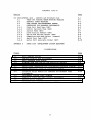
ILLOSTRATIONS
Figure
2-1
2-2
3-1
3-2
3-3
4-1
4-2
4-3
4-4
4-5
5-1
5-2
8-1
Basic GENISYS System
GENISYS Cardfile PCB Arrangement
Basic MICROLOK PLUS System
MICROLOK PLUS Application and Executive Software
MICROLOK PLUS Cardfile PCB Arrangement
Master/Slave Communications Programming Reference Diagram
ASSIGN Operators, Order of Precedence Samples
Queuing Option Reference Diagram
Conceptual Relay Models for GENISYS and MICROLOK PLUS
Programming
Development System Block Diagram
Example of Front and Back Contact Assignments
Queuing Option Example
Controller PCB Manually Selected Ootions
2-2
2-4
3-2
3-4
3-6
4-15
4-19
4-21
4-24
4-26
5-5
5-6
S-6
I
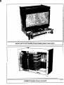
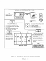
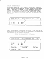
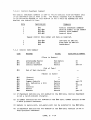
MICROLOK~ PLUS Cardfile (Cover closed, power drawer open)
'~
. '
I
. '
<
,l
,
_.,
•
•
,'
;
\
•
!
!I;~.
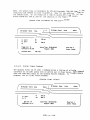
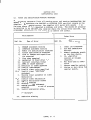
GENISYS® Cardfile (Cover removed)
I
I
SECTION I
INTRODUCTION TO MANUAL
1.1
PURPOSE
This manual provides instructions for programming the non-vital application
software of both the GENISYS ~on-Vital Loqic Emulator (NVLE) and the non-vital
section of the MICROLOK-PLOS Vital+ Non-Vital Control Package. These systems
share identical non-vital logic and interface circuit boards, as well as
executive and application software. PCB hardware and software design
revisions affect both systems.
1.2
FAMILY OF MANUALS
This manual is one of eight manuals that cover the GENISYS Non-Vital Logic
Emulator, the MICROLOK Vital Interlocking control System and/or the M!CROLO~
PLUS Vital+ Non-Vital Control Package. The following table summarizes these
manuals:
SM No.
system(s} covered
Purpose
6300A
GEN!SYS, MICROLOK PLUS
Both Systems: Programming of Non-Vita!
Application Logic
63008
GENISYS, MICROLOK PLUS
GEN!SYS: Hardware Installation, tocal
and Serial Data Interfacing, Pield
Troubleshooting
MICROLOK PLUS: Local/Serial Data
Interfacing and Field Troubleshooting
of Non-Vital Section (refer to SM-6400B
for MICROLOK PLUS hardware installation}
6300C
GENISYS, MICROLOK PLUS
Both Systems: Shop Troubleshooting of
Non-Vital Printed Circuit Boards
6301
GENISYS, MICROLOK PLOS
Both Systems: Installation of GEN!SYS
Development System CG.D.S.) - aacd and
Dual-Floppy Disks
6400A
MICROLOK, MICROLOK PLOS
Both Systems: Programming of Vital
Application Logic
64008
MICROLOK, MICROLOK PLUS
MICROLOK: Hardware Installation, Power
and Data Interfacing
MICROLOK PLUS: Hardware Installation,
Power Interfacing, Data Interfacing of
Vital Section (refer to SM-63008 for
non-vital data interfacing)
6300A, p. 1-1
SM No.
System(sl Covered
Purpose
6400C
MICROLOK, MICROLOK PLUS
MIC~OLOK:
?i~ld Troubleshoot!nq
MICROLOK PLUS:
Field Troubleshooting
of Vital Section
6401
MICROLOK, MICROLOK PLUS
Both Systems:
Installation of
MICROLOK Development System (M.D.S.l Har~ and Dual-Floppy Disks
6 300A, o. 1-2
1 --_.
SECTION II
GENE~AL INFORM~TICN - GENISYS
2.1
2.1.1
INTRODUCTION
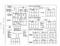
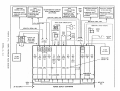
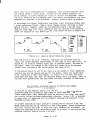
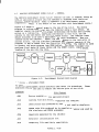
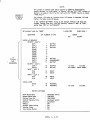
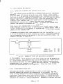
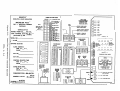
Ov~rall System (See Figure 2-1)
The GENISYS Non-Vital Logic Emulator (NVLEl is a general-purpose microcomputer and I/0 interfacing unit that can perform the functions of various
non-vital relay logic and digital logic systems, according to a customdesigned software program. This program uses a Boolean high-level language.
taking :nputs, performing logic and timing functions on those inputs and
produces outputs. The program is conceptually similar to a system of
interconnected relays. Typical aoplications include processing of central
office controls and local indications at a CTC system field station, and
processing of local indications for a local wayside control panel.
The basic hardware elements of GENISYS include a single microprocessor-based
controller printed circuit board (PCB), a power supply converter PCB and a
configuration of input and output FCBs determined by application. Three
optional output PCBs are equipped with 16 single-pole relay outputs for
various relay and/or control panel lamp driving applications. Two optional
input PCBs are equipped vith 16 optical-isolator res for interfacing of
contact-generated input signals. Power supply converter options ar~ tailored
for de voltages in the range of 9.5 to 35 Vdc and standard 120 Vac commercial
power.
GENISYS may be interfaced directly with a controlling computer, and with
digital carrier system modems. A Master/Slave protocol is used for
communications between a computer and GENISYS unit(s) or between two or more
units. Configurations may include (1) stand-alone units with no serial
communications links and (2) Master/Slave systems with serial conununications
links. Master/Slave systems may, in turn, incorporate one or more Master
GENISYS units. These configurations are shown in Figure 2-1.
Communications options include EIA RS-423 (RS-232C compatible) or
TTL-compatible. Modems are required when more than one Slave unit is
connected to a Master unit, or when direct-interface communicat ion·s limits ar~
exceeded. Each GENISYS unit may control a total of 256 inputs and outputs in
any configuration, including those where inputs or outputs are absent. Up to
255 Slave units may be controlled by a Master unit, however the typical
practical limit is in range of 40 to 50 units.
2.1.2
Application and Executive Software
The GENISYS system incorporates independent Application and Executive
software. These are contained in separate EPROM chips on the Controller board.
The Application software or logic is developed for the specific installation,
either by OS&S or the customer. The source program is written and •compiled•
on a computer, using a language that enables the system logic to be expressed
in terms familiar to the railroad engineer. The finished program is converted
into a form that can be entered or •burned• into the EPROM chips.
6300A, p. 2-1
MASTER PORT
TO NON-VITAL
SLAVE UNITS
12
voe
110
POWER
SUPPLY
RS-4231
lls-232(
OR
SLAVE PORT TO
NON-VITAL MASTER,
OFFICE COMP.,
...
LOCAL PANEL, ETC
12 VD(
sv Ill
CONTROL
RELAY
COILS
'
INOICA.
RELAY
CONTACTS
'°.,c::
,I)
)"
CIITRL.
PCB
I
I
OPJO
IN
llfLAY
CONl.
OUT
M • MASHR PORT
5 • 5LAVI PORT
---1 .
,
11,v,dl.llOUS
•
PWR.
I
CONI.
RELAY
OUT
OPTO
II~
•
lll
-0
I-'·
()
N
G)
I
",.,)
LOCAL
1/0
t'l
z
TOTAL LOCAL VO PER UNIT:
H
(/)
•<
RflAY·OUJPUT PCIS
Ul
en
• 256 RELAY-OUTPUT AND/
OR OPTICAL INPUT
• 256 RELAY-OUTPUT ONLY
• 256 OPTICAL-INPUT ONLY
OPTICAl·INPUT PCIS:
1UtRPCI
•
Ii Plll PCI
N451441·JHI:
•
N451441-SIOl,
IT
IXTlRNAL·STROIE
fl)
•
OUTPUT
N4Sl441-41tl:
1mm
1
fOR CAIIU UNGJH
OVER 50 fl,
111' RS·4H IIIS-lllC
COMPATIBLE)
5V TTL • USlS
DCHOU MODEM
PWR
corn
ktlAY
OPIQ
OUI
114
D£SICiN MAX.• lSS Sl>,lillS
N4S\44\·U01:
5 TO U VDC
INPUT !ASSURED
t
J.
MA STER
CENTRALIZED
CONTROL
c
p
OUl
IN
,
c
~-..
l
SlAVf
SL I Vt
S 1.1
S M
S M
INPUTS
•
OUl
IN
p
c
OUI
Ill
5 voe TIIRfSHOLD)
N4Sl441·1101:
CONSTANT $1ATI
AT POWEi Off
s
PWR.
SLAVE
SERIAL 1/0 • SYSTEM CONFIGURATIONS
s To u voe
INTERNA.l·STROlf
OUTPUT
t
11,
PRACTICAL LIMIT • 4S Tll SO SLAVfS
•
a
0~10
M • MASTlR POIIT
S • SLAVE PORT
•
·.:
(I)
IIUAY
Olli
CONI
PWII
I~~·~:~ ,......... .
l
I
co,
CAkPfll E BUS
Ill
Ci] (ii)
u1 lMI 1
PCB
POWER
tD
SLAVE
i •
SERIAL 1/0 • MODEM INTERFACE
MASTER
w
0
0
I
GENISVS•
"'.....
•
OPllCAL•
ltlPUl
PCBS
POWER
SUPPL y
CONV.
PCB
I
(1\
RS·UJ: 50 FT. MAX.
5V TTL: S fJ. MAX
[il~
PWII
POWER SOURCE
9.5 TO 35 voe
OR 120 VAC
I-'•
,. •
M A.STER
II
...,
SERIAL 1/0 • DIRECT INTERFACE
CONT,
RHAY
OUT
•
OPTO
IN
DISTRIBUTED
CONTROi.
p
'
OUl
~
l
S 1,1
5 M
f,,4
IN
p
'
.,.
+l
001
IN
p
'
OUI
IN
GE~ISYS ~ay be programmed by using the GENISYS Develooment System (G.D.Sl.
~his system enables the user to design and test his own program, and then load
it into the system hardwar~. The G.D.S. consists of a personal computer, an
EPROM Programmer and the GENISYS software, which is cont3ined on a single
diskette. The G.D.S. can only be employed with the programming equipment
supplied by OS&S.
The Executive software is coimnon to all GENISYS systems. This software
performs input, internal and output logic operations defined in the
application logic.
This manual edition covers all software versions up to and including Executive
Software Version 11 and Application Compiler Software Version 3.0.
2.2
2.2.l
COMPONENTS
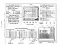
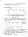
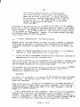
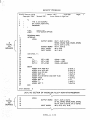
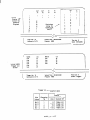
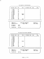
Cardfile (see page v and Figure 2-2)
The GENISYS Non-Vital Logic Emulator is housed in a standard 19 inch
rack-mount cardfile. The cardfile always contains a power supply converter
PCB in the far lefthand slot, a controller PCB in the second slot and between
zero and 16 relay-output and/or optical-input PCBs in the remaining slots.
When relay-output ?CBs are present, they are always placed as a group to the
left of any optical-input PCBs. Empty slots are allowed between relay-output
and/or ootical-input boards provided these slots are defined as •spares• in
the application program. For example, in Figure 2-2, empty slots 7 and 8
("spare•> allow future expansion of outputs without having to reconfigure the
inputs.
6300A, p. 2-3
EXAMPLE: S RELAY OUTPUT PCBS ONLY
SLOf NO. -
1
2 3-------
EXAMPLE: 7 OPTICAL-INPUT PCBS ONLY
18
SLOT NO. -
I
t
1ST OPTICAL-INPUT PCB
EXAMPLE: 4 RELAY·OUTPUT AND
4 OPTICAL-INPUT PCBS
GENISYs· PLUG-IN CIRCUIT BOARDS
,.
2•
3-18
3 - - - - - - - - 18
t
1ST RELAY-OUTPUT PCB
SLOT
NO.
l
DESCRIPTION
PART NO.
POWER SUPPLY (9.5 - 35 VOC)
POWER SUPPLY (120 VAC)
N451441-4601
CONTROLLER
N451441-5602
t
N4S1441-7601
RELAY-OUTPUT OPTIONS:
CONTROL DELIVERY
N451441-3601
CONSTANT DELIVERY
N451441-7101
CONTROL ANO DELIVERY
N451441-4701
OPTICAL-INPUT OPTIONS:
OPTO-INPUT(HIGH THRES.)
N451441-7202
OPTO-INPUT (WIDE RANGE)
N451441-S802
SLOT '10.
: : : : : :
: : : : : :
- J
ff L
1
2
3
9
!ST RELAY·
OUTPUT PCB
•THESE PCBS ALWAYS IN THESE SLOTS
Figure 2-2.
~
: :
.
.
: : : :
: : : :
;
;
!j
:
:
J
19
IST OPTICAL>NPUT PCB
SLOTS 7 ANO 8 EMPTY; MUST BE DEFINED
AS ·sPAREs· IN APPLICATION PROGRAM.
GENISYS Cardfile PCB Arrangements
6300~, p. 2-4
2.2.2
2.2.2.1
PCSs
Controller ~451441-5602
~he Controller PCB performs all logical decisions and calculations for the
GENISYS system, and serves as the remote communications interface for any
external devices. Primary functions include management of local !/0 (via card
file interface boards) and remote I/0 (via serial data line) according to the
custom-design program, and execution of internal watchdog and testing routines.
2.2.2.2
Relay-Output PCBs
US&S provides three different relay-output PCBs for the output group of the
GENISYS cardfile (see Figure 2-2). The cardfile need not contain any
relay-output PCBs, or may contain these PCBs in all cardfile slots (maximum of
16). Applicable PCBs are as follows:
PCB Name
Part Number
Operating Type
Control Delivery
Constant Delivery
control and Delivery
N451441-3601
N451441-7101
N451441-4701
Pulsed Deli very
Stick Relays
Internal Strobe
The -3601 PCB is the standard GENISYS output board.
used for special applications.
2.2.2.3
The remaining boards are
Optical-Input PCBs
OS&S provides two different optical-input PCBs for the input group of the
GENISYS cardfile (see Figure 2-2). Each is designed to handle different input
voltage ranges and types. The cardfile need not contain any optical-input
PCSs, or may contain these PCBs in all cardfile slots (maximum of 1;1.
Applicable PCBs are as follows:
Name
Part Number
Indicat ion-Opto
Ind icat ion-'Jpto
N451441-5802
N451441-7202
~he -7202 PCB is the standard GENISYS input board.
2.2.2.4
Power Supply Converter PC3~
US&S provides two power supply converter PCBs for GENISYS which output
operating power for other cardfile PCBs, and power for the carrier monem
interface (+/- 12 Vdc) when required by application. These are as follows:
Part Number
Input Voltage
N451441-7601
N451441-4601
9.5 to 35 Vdc
120 Vac (nom.)
6300A, p. 2-5
2.3
SPECIFICATIONS (Programming Related)
Total Si:s:
1450 bits maximum (can be divided
between local I/0, serial I/0 and
internal)
Local I/0 Boards:
16 maximum per cardfile (any
combination)
Local I/0 Bits:
16 maximum per local I/0 board
Master-to-slave Communications:
255 Slave units maximum, communication
from Master unit.
Slave-to-Master Communications:
1 Master unit maximum, communication
from Slave unit.
Serial Addresses:
1 to 255 inclusive
Serial Baud Rates:
so, 75, 100, 134, 150, 300, 600, 1200,
1800, 2400, 3600, 4800, 7200, 9600
Active Timing Elements:
100 maximum active at
any one time in
application logic (more timers may be
defined).
Logic Equations Triggered:
1000 maximum, one-queue option, 500
maximum each queue, two-queue oction
(refer to page 4-21).
6300A, p. 2-6
I
SECTION III
GENERAL INFORMATION - MICROLOK ?LOS
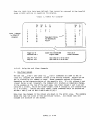
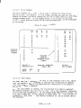
3.1
3.1.l
INTRODUCTION
Overall system (See Figure 3-1)
The MICROLOK PLUS Vital and Non-Vital Control Package is a multi-purpose,
microprocessor-based device designed for use in both vital and/or non-vital
railroad control systems. It is typically used for smaller applications, such
as a single end-of-siding, that do not require the large input/output
capabilities of seperate vital and non-vital controllers. The device can be
configured with a vital control section only, or with vital and non-vital
control sections. (A non-vital-only configuration is also possible, but not
typical.)
In a typical single end-of-siding application, both 3ections are utilized.
The vital section controls the interlocking logic, manages switch machines,
signals and track circuits in the control area; while the non-vital section
provides an interface point for a local control panel, processes CTC office
conunands, and transmits indications from the vital section. Another typical
end-of-siding configuration could consist of the vital section only, with code
system inputs and outputs processed within the vital section (no local control
panel).
The MICROLOK PLOS system is derived from the OS&S MICROLOK Vital Interlocking
Control System and the GENISYS Non-Vital Logic Emulator. rt uses the same
plug-in printed circuit boards, the same Executive software, and the same
application logic compilers as the MICROLOK and GENISYS systems.
3.1.2
Non-Vital Section
The non-vital section of MICROLOK PLOS incorporates a Master port that enables
the device to serve as the managing unit of a non-vital Master/Slave system.
Up to 255 Slave units can be controlled from this port, although the oractical
upper limit is about 40 to 50 units. The Slave units for such a system might
include additional M!CROLOK ?LOS or GENISYS units, or a combination of both.
The non-vital Slave port enables the unit to function as a Slave to another
Master unit. The Master unit can i~clude another MICROLOK PLOS unit
(non-vital section), a GENISYS system or an office comcut~r.
When the application requires a serial link between the non-vital and vital
sections of the MICROLOK PLOS unit, the non-vital Master port is used for this
purpose, while the Slave is used for external conununications.
Non-vital serial link conununications are formatted to EIA RS-423 standards,
and derated to operate under the RS-232C standards. This enables the MICROLOK
PLUS non-vital serial ports to be interfaced to an ETA-compatible modem for
remote conununications.
6300A, p. 3-1
NON-VITAL
CONTROL SYSTEM:
• MICROLOK PLUS™
(NON-VITAL SECTION)
•GENISYS•
VITAL
CONTROL SYSTEM
(MASTER)
• MICROLOK PLUS IM
(VITAL SECTION)
•MICROLOK•
VITAL
CONTROL SYSTEM
(SLAVE)
• MICROLOK PLUS1M
(VITAL SEC, CODE)
• MICROLOK• (CODE)
SEE SM·6300B FOR COMPLETE
SERIAL COMMUNICATION
LINK OPTIONS
NON-VITAL CONTROL
SYSHM (MASTER):
NON-VITAL CONTROL
SYSTEM (SLAVE):
NONVITAL
LINK
11
• MICROL OK PLUS,,.,
(NON-VITAL SECTION)
1
•GENISYS
• OFFICE COMPUTER
• MICROLOK PLUS "
(NON-VITAL SECTION)
•GENISYS•
NON·VITAL SERIAL LINK
,----------------------------,
:
VITAL LOCAL CIRCUITS (TYP .)
:
VIT Al SERIAL LINK
:~
NON-VITAL SERIAL LINK
:
~NI
SlAkClll l. DRIVE
'1J
.....
,.,c::
SIGNAi
LAMP!,
+
11)
w
.
I
......
0\
w
0
0
)>I
-0
w
I
N
CUT-OH
RELAY
(VCOR)
lJ
w
....
(I)
POWER" FOR
RELAY AND
LAMP DRIVE
OUTPUTS
·w
OPTIONS:
~
~
["'1
"Cl
II
.~.
H
()
12 voe
BATTERY
PRO·
CfS\OR
PCB
·u
voe
·12
VO(
~b
~
I
W
VITAi
MAST.
PORT
II
VD(
-
I
M S
PORH
JfQ
CODE
Pf RI·
SID.
81·
DC
STD.
STD.
CON·
\nllM
Ullfflf.
PtlfRAl
PCB
OR
VOLi.
POLAR
RflAY
LAMP
DRIVER
lllPUl
PCB
INPUT
PCB
11\0llfll
PCB
PCB
PCB
llMHED
RELAY
OfllVtll
PCB
ORIV£11
PCB
PCB
c
C/)
Cl)
·<
12 VD(
BATTERY
II
RUAV·
OUlPUI
fCB
I
OPIO
IIIPUl
Bl·
POLAR
COllflG
PCB
I
TOTAL 1/0
----- SLOTS: 10
II)
(1"
r ,
II)
VITAL CPU --•:~
:3
VITAL-'·
BUS
24 VDC SUPPLY
:·
: VITAL 1/0 - - ~ - ~
NON-VITAL
SECTION
VITAL SECTION
I
t t l t
j
(OIHA(I!,
I
BU\
INIERF
["'1
lll!Jl(A 11014
llflAY
h-~---~----------------------~
OPTIONS:
I I ·u
·~·
I
3:
0
a•
aJ
Rh A~
~
0
:,q
COIHROL
RELAY
COILS
"J~w.
ll.M4CH
VIT .114
DI
~----------------------------~
NON-VITAL LOCAL CIRCUITS
I
~ ,
ul
NON-VITAL SERIAL LINKS
Rer-·i
I
T
t t t J
POWER SUPPLY CONVERTER
It
I
f J_
I
NON-VITAL
BUS
3.1.J
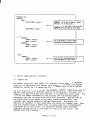
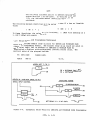
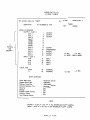
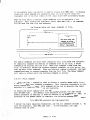
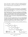
Aoolic3tion and Executive Software (See ~igure 3-2)
Sach section {vital and non-vital) of the ~IC~OLOK ?LOS unit incor~orates its
own, independent Application and Executive software. These are contained in
EPROM chips on the logic boards of the respective sections.
The Application software or logic in each section is developed for the
specific installation, either by OS&S or the customer. The source program is
written and •compiled• on a computer, using a language that enables the system
logic to be expressed in terms familiar to the railroad engineer. The
finished program is converted into a form that can be entered or •burned• into
the EPROM chips.
The MICROLOK PLOS non-vital application logic can be develooed using the
optional GENISYS Development System (G.D.S.). This system enables the user to
design and test his own program, and then load it into the system hardware.
The G.D.s. consists of a personal comouter, an EPROM Programmer and the
GENISYS software, which is contained on a single diskette. The G.D.S. can
only be employed with the programming equipment supolied by OS&S.
The Executive software of the vital and non-vital sections of MICROLOK PLUS
are common to all units. The non-vital section Executive software performs
input, internal and output logic operations defined in the non-vital
application logic.
This manual edition covers all software versions up to and includinq Executive
Software Version 11 and Application Comoiler Software Version 3.0.
6300A, o. 3-3
MICROLOK• AND GENISYs• DEVELOPMENT SYSTEMS
PC
•
D[]ti ___ -- .
COMPILE ANO SIMULA TE l l i D ~ I J D = C A B L E
APPLICATION LOGIC.
-,
I~=========~~~ J
I
__
EPROM
PROGRAMMER
•
•
_©__,15--
,---
CJ
,• ;--u--:
@
--- -- ______...
CHECK EPROM
LOAD APPLICATION
LOGIC.
APPLICATION
LOGIC EPROIIA
8K X 8
i.ema
PERIPHERAL PCB N451441·5502
DEVELOPMENT SYSTEM SOFTWARE FOR PC
•
THREE EXECUTIVE EPROMS (IC20, 21. 22)
•
UP TO THREE APPLICATION LOGIC EPROMS
(IC 15, 16, 19)
•
USES MICROLOK• DEVELOPMENT SYSTEM
FOR APPLICATION LOGIC EPROMS
•
•
•
,,
_1_
CODE SYSTEM INTERFACE
PCB N451441-S302
•
ONE EXECUTIVE EPROM
{IC14)
CPU
110 BUS
CODE
PERI·
I/ITAL
CON-
PCB
lNUl\f.
SYS.
INTEl\f.
PttEl\AL
110
Tl\OLLEII
PCB
PCBS
PCB
PCB
•
DOES NOT USE APPLICA·
TION LOGIC EPROMS OR
DEVELOPMENT SYSTEM
PCB
-
.. ..
___[___ VITAL SECTION
COMPILER PROGRAMS
SIMULA TOR PROGRAM
EPROM PROGRAMMER DRIVER
--
NON•
I/ITAL
110
.•
PCBS
NON·
VITAL
SECTION
_J_
MICROLOK PLUSTM
CONTROLLER PCB N45144t-5602
•
ONE EXECUTIVE EPROM (IC29)
•
APPLICATION OPTION: CODE SYS.
EMULATION, OR:
•
UP TO 5 APPUCA TION LOGIC
EPROMS (IC 24, 25, 26, 27, 28)
•
USES GENISvs· DEVELOPMENT
SYSTEM FOR APPUCA TION LOGIC
EPROMS
NOTE
NON-VITAL APPLICATION LOGIC
COVERED IN THIS MANUAL REFER
TO SM-6400A FOR VITAL APPLICA·
TION LOGIC PROGRAMMING.
Figure 3-2.
MICROLOK PLOS Application and Executive Software
6300A, p. 3-4
3.2
COMPONE!-lTS
3. 2. i
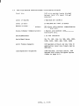
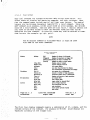
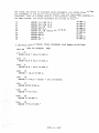
Cardfi le ( see paqe ,, and Figure 3-3)
The MICROLOK PLUS package is housed in a printed circuit board cardfile
designed for mounting in a standard 19 inch ~uipment rack. Vital section
boards are ?laced in the ten left-most slots, while non-vital boards are
placed in the three right-most slots. 'l'he non-vital section is controlled by
a single Controller PCB. Two slots are provided to the right of the
Controller PCB for local interfacing. When the application requires only one
relay-output
optical-input board, this board is always installed in slot
P. When the application requires one relay-output and optical-input board.
the relay-output board is always installed in slot ~nd the optical-input
board is a-lways installed in slot Q.
or
3.2.2
3.2.2.1
PCBs
Controller N451441-5602
The Controller PCB performs all logical decisions and calculations for the
MICROLOK PLUS non-vital section, and serves as the remote communications
interface for any external devices. Primary functions include management of
local I/0 (via card file interface boards) and remote I/0 (via serial data
line) according to the custom-design program, and execution of internal
watchdog and testing routines.
3.2.2.2
Relay-Output PCBs
as&s provides three different relay-output PC3s for the MICROLOK PLUS
non-vital section outputs. Applicable PCBs are as follows:
PCB Name
Part ~umber
Operating Ty-pe
Control Delivery
Constant Delivery
Control and Delivery
~451441-3601
N451441-7101
N451441-4701
Pulsed Deli very
Stick Relays
Internal Strobe
The -3601 PCB is the standard MICROLOK PLOS non-vital output board.
remaining boards are used for special applications.
3.2.2.3
The
Optical-Input PCBs
OS&S provides two different optical-input PCBs for the MICROLOK PLOS non-vital
section inputs. Each is designed to handle different input voltage ranges and
types. Applicable PCBs are as follows:
Name
Part Number
Indication-Opto
Indication-Opto
N451441-5802
N451441-7202
The -7202 PCB is the standard MICROLOK PLOS non-vital input board.
6300A, p. 3-5
FRONT
VITAL SECTION PCBS • CPU
I SLOT
PART NO.
A
c
D
NON-VITAL SECTION
Pl<OCfSSOR
1/0 BUS INTlRI ACf
CODI SY!olfM lllltRfAC!
PlklPttlRAL
N451441·5101
144514-11-600 I
N4Sl44H302
114S 144 I-SS02
8
II
VITAL
CPU
IHS 1 AILA IION
....
...,
.....
'°....
5101
SIOl
SIOl
SI Ol
l'ROCISSOR
IO BUS INIERIAC[
SYSHM U41ERIAC!
PEIIIPHtkAL
coot
K L M N OPQ
ABCDEFGH
DESCRIPTION
1~
A. All VllAL APPLICAl1om
b. All VITAL APPLICATIONS
C, WIIEN RfQ'D BY APPIICAIIOf~
0, All Vff Al Al'l'LICA 110145
..
.~VU!~.
l..m I I .
VITAL SECTION
•
•
.
:,.;
H
()
:0
CJ)
w
0
0
..:,:.,
.,.
w
I
:)\
0
t-t
~
I SLOT
I O
l • N
j
I
't1
t"'
I
NON-VITAL SECTION PCBS · 1/0
I SLOT
: ...
DESCRIPTION
STANOAKD RELAY ORIV(R
VOLl ·llMll kll AV DRIVER
81·POLAII KHAY DRIVER
DC IAMP ORIVffl. Ill W IAMP
DC LAMP ORIVlR. 2S W LAMP
DC LAMP DIIIVIR. 36 W LAMP
ST ANOARO INPUT, 12 V NOM
SJANDARO INPUI, 24 V NOM.
N451441·8601
N451441·8501
N4S 1441 ·810 I
N451441·6102
N4S 1441-6703
N4Sl441-7301
N4S 1441·8802
N4S 1441·1803
I
CONIROllfR
I
VITAL SECTION PCBS • 1/0
NO.
N4Sl44H602
I
DESCRIPTION
lllSTAILAIION
P, Q
I SLOT I PART
PART NO.
\LOl 0, All N014-Vl1Al APPllCAllOUS
i::
11)
w
I
w
NON-VITAL SECTION PCB · I.OGIC
---.-----....------------1
N4Sl441·3601
N451441·7101
N45144H101
ll4S1441·1202
N4S 144 l·S&02
I
DESCRIPTION
PART NO.
COIIIROI OfVIIVtkYl
COtlSTANl OILl~Hn
CONlROl° & DfllVIRY
OPIO·lflPUl (ltlGtt IIIIIB11Ul0)
OPIO·INPUI (WIOt I\AUGl)
INSTAllATIOU
Otlf RUAY·OUTPUI: SlOl I'
ONE OPlO·INPUf: SIOl P
ONE RElAY·OUTPUT AND ONE OPIO·INl'l)l.
llflAY IN UOl P. OPJO IN SIOl Q
.uv
OUIPUI
lf(J
IN\lALLATION; \£1 El<AMPlES llllOW
c:
·UV
OU I PUT
IED
tSV
·SV
OU I PUT
LEO
OUIPUl
110
24V
INPUl
LID
POWER SUPPLY DRAWER
en
44·WAY PCB
EDGI COIINfCTORS
(VITA~ VO ANO
All NOll-VIIAL PCBS)
VIIAL
MAHER
PORT
H·PIN ·o•
CODE
l>YSHM
POl<l
l~·PIII •p•
VITAi
SIAVt
Pukl
lll'Ui
()
Ill
....
a.
CARD SLOT ID - . , OPQ N M
....
.....
"II
VITAL 1/0 INSTALLATION EXAMPLES
II)
't1
()
tlJ
EXAMPLE: 6 OUTPUT PCBS
ONLY
1111
>
....
....
EXAMPLE: 5 INPUT PCBS ONLY
111-1:::-,
' ' I 1:::
VITAL 1/0
QI
::s
'°~
11)
111
::,
rt
ft: (((
1
I
I
I
I
I
I
I
I
I
I
I
I
I
I
I
I
I
I
I
I
I
I
I
~·
VITAL 1/0
I:::
1:::
1:::
1:::
1:::
I I
I I
I I
I I
I I
I I
I I
I I
1:::
1:::
1:::
I I I 1;;;
L
III!!!
15T OUTPUT PCB
IN SLOT E
L
t
t
oror
tt:
I
I
I
I
I
I
I
I
I
I
I
I
I
I
I I
1ST INPUT PCB
IN SLOT E
'-y-'
A&:TIA/1:S:M
I I
II I I I I
I
~
NO EMPTY SLOTS
I
I
I
I
I
I
I
I
I I
lllll!ll
VITAL 1/0 ft:
I
I
I
I
I
I
ft#'_.,
I
I I 1:::
I I 1:::
I
I
I
I
I I 1:::
. • • • • ,,,111::;
L
L
151 INPUT ~CB
IN SLOT I
IST OUTPUT PCB
IN SLOT E
L-y---'
NO EMPTY SLOTS
n,...,,,,rr•'
EXAMPLE: 4 OUTPUT PCBS
3 INPUT PCBS
NO FMPTY <lf)H
14 V !NPUJ
JlllMIHAL\
VCOII l.lUJl'UI HlllollllALl
·o·
I
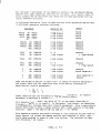
3.3
NON-VITAL SECTIOM S?ECIF!C~TIONS (Proaramming Related)
Total Sits:
1450 bits maximum (can ce divided
between local I/0, secial I/0 and
internal)
Local I/0 Boards:
2 maximum per cardfile
Local I/0 Bits:
16 maximum per local I/0 board
Master-to-Slave Communications:
255 Slave units maximum, communication
from Master unit.
Slave-to-Master Communications:
1 Master unit maximum, communication
from Slave unit.
Serial Addresses:
1 to 255 inclusive
Serial Baud Rates:
so, 75, 100, 134, 150, 300, 600, 1200,
1800, 2400, 3600, 4800, 7200, 9600
Active Timing Elements:
100 maximum active at any one time in
application logic (more timers may be
defined).
Logic Equations Triggered:
1000 maximum, one-queue option, 500
maximum each queue, two-queue option
(refer to page 4-21).
6300A, p. 3-7/8
SECTION IV
PROGRAMMING ?ROCEDURES - GENISYS AND MICROLOK PLUS
4.1
GENERAL
In the non-vital apolication program, various bits (input, output, internal
etc.) and logic procedures are defined in a text nata file on a computer.
Input and output statements are described by location. They can be local r/o
connected directly to that unit, or remote !/0 on either of two serial lines
(Master, Slave). Timing values indicate the set (pick-up) and/or clear
(drop-away) delays of the bits. Boolean statements are used to describe the
system logic. The completed •written• program is referred to as the source
program. It is processed by the compiler and converted into data tables. In
turn, these tables are •burned• into one or several EPROMs: the EPROM(s) are
then installed into the Controller PCB. Sections 4.3 to 4.8 describe how
these basic programming operations are handled with the OS&S GENISYS
Development System CG.o.s.>.
4.2
PROGRAMMING LANGUAGE
4.2.1
4.2.1.1
Terms
Character Set
The Character Set consists of the full ASCII character set, as defined Eor the
user's computer. These are listed in Table 4-1. Only certain characters may
be used to make up user-defined symbols <refer to section 4.2.1.3). Although
all letters are acceptable, all lower case letters Ca-z) are converted to
upper case CA-Z) by the system. ?or example, •stick• is read the same as
•sTICK•. Lower case is only used for readability.
Table 4-1.
Character Set
FOR USER-DEFINED SYMBOLS
SPECIAL CHARACTERS
SPECIAL CHARACTERS
Opper Letters
tower Letters
Numerals
Period
Dollar Sign
Underscore
Colon
Semicolon
Comma
Equal Sign
Open Parens.
Close Parens.
Backslash
Percent Sign
At Sign
Plus Sign
Asterisk
Tilda
CA-Z)
Ca-z)
C0-9)
.
$
=
6300A, p. 4-1
,
i
!
+
*
..r>
I
4.2.1.2
Reserved Wor~s
~ Reserved NOrd has a predefined ~eaning to the comoiler.
Words ar~ listed in Table 4-2:
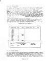
Table 4-2.
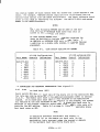
PROGRAM
INTERFACE
LOCAL
MASTER
SLAVE
4.2.1.3
OUTPUT
INPUT
WORD
VAR
TIMER
The 25 ~eser7e~
GENISYS Reserved Words
SET
CLEAR
BEGIN
AND
OR
NOT
END
XOR
ASSIGN
TO
MSEC:
SEC:
MIN
ADDRESS
SPARE
User-Defined Symbols
User-defined symbols are used to create relay names in the source program.
These symbols must contain characters from the first part of Table 4-1, and
cannot consist of all numbers. A maximum of 12 characters may be used to
create symbol names.
Examples of legal symbols in G.o.s. Versions 1.01 and higher include:
relay.123
• INPUT RELAY
INSTRK$1N
DOG
lTK
Illegal examples of the above symbols in G.D.S. Versions 1.01 and higher
include:
• INPUT .RELAY .1
RELAYU
123
(Exceeds 12 character maximum)
(Contains an illegal character)
( all numbers)
E:<amples of legal symbols in G.o.s. Version 1.00 include:
relay.123
.lTK
.!NPUT RELAY
INSTRKSIN
DOG
Illegal examples of the above symbols in G.D.S. Version 1.00 include:
lT!<
.INPUT.RELAY.!
RELAYtl
(Begins with number)
(Exceeds 12 character maximum)
(Contains an illegal character)
6300A, o. 4-2
I
4.2.1.4
Delimiters
Delimiters separate individual words.
language are listed in Table 4-3.
Table 4-3.
space
tab
colon
backslash
•at•
,,>
(
:)
( @)
semicolon
equal sign
comma
percent
plus sign
Delimiters in the non-vital program
Delimiters
( ; )
( =)
(
I )
( %)
( +)
open parenthesis
close parenthesis
carriage return
tilda
Asterisk
c()
{)}
(CR)
""
(*)
Every distinct word or token in the source program must be separated by one of
the above delimiters. Extra space and tab delimiters may be inserted anywhere
in the program: they have no effect on the meaning of the program.
4.2.2
4.2.2.1
Formats
General Arrangement of Statements
source program statements may begin anywhere on a line with tabs.
Non-significant spaces are ignored by the compiler. If a statement is too
long to fit on one lin@, it may be continued to any number of following lines
as required. The maximum allowable line length is 100 characters. If this is
exceeded, an error message will be generated. ~lthough the non-vital compiler
uses a free format, statements should be arranged for easy reading.
4.2.2.2
Non-Program Comments
Miscellaneous comments may be inserted in the source program to aid the user
in charting and reviewing the program. To distinquish a non-program comment
from program statements, begin the statement with a{%) and end with a
backslash(\). For example:
w
THIS IS AN EXAMPLE OF A LEGAL GENISYS OR MICROLOK PLOS COMMENT,
When the compiler encounters the percent(~) sign, characters are ignored
until it reaches a backslash (\). Switches are the exception (refer to
section 4.2.2.3). Note that comments may begin anywhere (including the middle
of a statement) and span any number of lines in a source program. qowever,
they cannot begin in the middle of a word ( ASSI%,GN is illegal). HencP.,
another example of a correct comment is a follows:
'
THIS IS AN EXAMPLE OF
A LEGAL GENISYS OR MICROLOK PLUS
COMMENT
The closing backslash(\) must be inserted, otherwise the compiler iqnoras all
other characters until a backslash is found.
6300A, p. 4-3
I
.
.......
_
Compiler Version 3.0 and 3igher - Note the in the orogram example on page 4-JC
that an ~xc!amation ~oint apoears before each comment. This character only
appears if the comment is the first non-blank item on the line or scans
multiple lines and is automatically inserted after the line number to help
distinguish the comment from other parts of the program. Thus, if the closing
backslash is accidentally omitted from the comment, the exclamation point ·11ill
appear after every line number to indicate that the compiler regards all
subsequent lines as comments, rather than other tvpes of program statements.
4.2.2.3
Compiler Switches
Compiler switches are used in the source program to select various options
such as baud rates. (Refer to Section 8.4 for hardware switch ootions.l
Compiler switches begin with a percent sign(%) (like non-program comment)
To distinquish it from a comment, a dollar sign CS) must be placed
immediately after the percent sign.
After the dollar sign is a single letter representing the switch nam~.
Hext is a character(s) representing the value of the switch.
All characters after the value character(s) are ignored by the compiler until
the next backslash symbol C\).
Example
Comment
%SS3\
Sets switch •s• to value 3.
%SD- THIS IS A COMMENT FOLLOWING THE SWITCH'
Sets switch •n• to off.
Remainder is a comment.
Compiler switches are as follows:
dsn\
Set the Saud Rate on the Slave Port (where n
=
I through Hexadecimal~
This value is defined on the hardware switch or in the source program, and is
a single character. If no Slave baud rate switch is present in the source
program, the rate set on switch SWl will be used. Software values for this
function are listed in Table 4-4 on page 4-7.
NOTE
In Executive software revisions O through 10 of the
following switch (%SMn), a setting of n = 0 would
generate an error. The revision 11 function is
as follows:
%3Mn'\
Set the Baud Rate on Master Port (where n
a
O through Hexadecimal Z)
This value is set only in the source program, and is a single character. If
no Master baud rate switch is present in the source program, the default rate
is 1200 BPS. If •o• is specified, the compiler defaults to the setting on
rotary switch SWl on the controller PCB. Softwar~ values and associated baud
rates are listed in Table 4-5 on pa9e 4-7.
6 300A, p. 4-4
NOTE
The following compiler switch ciiPxxxxl applies to
GENISYS Development System 7ersions 1. 02 and higher
and :!xecuti ve PROM IC29 Revision 7 and higher. This
switch is not available with earlier versions.
\SPxxxx\
Specify the Master No-Response Time-Out (where x: 100 through 99991
This value is set only in the source program. It specifies the number of
milliseconds the Master will wait for the Slave to begin responding. If the
Slave has not responded within this time, the message is considered bad and
the Master will continue with the polling cycle. The value entered is rounded
upward to the next multiple of 100. For example, %SP735\ (polling time-out•
735 milliseconds) would instruct the executive software to wait 800
milliseconds for the Slave to respond. If this switch is not specified, the
default is 1 second.
i:kon\
Set the Control Delivery time (where n: 1 through Hexadecimal F)
This value is the duration of the Controller PCB delivery pulse to the relay
output PCB(s). rt is defined on the hardware switch or in the source program,
and is a single character. If no •so• switch is present in the source
program, the Control Delivery time set on switch SW2 will be used. Software
values are listed in Table 4-6 on page 4-7.
NOTE
The following compiler switch C%Scv,) applies to
GENISYS Development System Versions 1.01 and higher.
In version 1.00, this switch is listed as Security
On/Off. (There is no operational difference between
the two Versions.)
1$Cv\
Security On/Automatic (where v =+or-)
Slave unit polling from a Master port in a GENISYS or MICROLOK PLUS system can
occur with or without CRC security (refer to protocols in Section VII). The
CRC security is either •+• (send poll with CRC security) or •-• (automatic
on/off CRC security for poll). ~hen the•+• value is selected, the Master
unit will always send the secure form of the polling commana. If the•-•
option is selected, the security is automatically included when the Master
determines that the line is sufficiently noisy to warrant it. The default for
this option is \SC-\ (automatic CRC inclusion).
%.SVv\
Validate Value (where v
=+
or -)
rhis switch is used to inform the Executive software whether or not to wait
for validation before an output is performe1. Refer to sections 4.2.5.4 and
5.3 for detailed descriptions of this switch. The value (v) of this switch is
either plus or minus C+/-). Plus corresponds to option •on• and minus to
option •off•. The default for this switch is %SV+\ (validation on).
i:;300;1., !'· 4-5
I
%$Dv,
Debug (wher~ v =+or-)
G.o.s. Versions 1.01 and Higher:
This switch informs the compiler that the simulator will be used to debug the
program. When this switch is turned on ( %SD+\ ), the compiler retains, in a
separate Eile, relay names assigned in the application program so that these
names may be used when simulating the application logic. Programs to be run
on the simulator must have the D+ switch. The program does not have to be
recompiled with %SD-\ to permit programming of PROMs. The default for this
switch is \SD-\.
G.o.s. Version 1.00:
(Same function). After debugging, the program must be recompiled with %SD-\
to permit programming of EPROMs. The default for this switch is %SD-\.
\SQv\
Queuing (where v =+or-)
This switch sets the number of logic queues to be used. One queue or two
queues may be selected. Refer to section 4.2.5.2 for a detailed description
of this switch.
~!av,
Symbol Table Listing (where v =+or-)
This switch inhibits the symbol table from being placed in the list file.
When set to %SB-\, this switch turns off the symbol table at the bottom of
the compiler listing. If the validation switch (refer to previous page) is
enabled, the program should be compiled with the symbol table enabled before
the PROM is programmed. This will insure that no unassigned outputs e~ist.
If any exist, they should be assigned values and the program recompiled to
avoid validation errors. The default for this switch is %SB+\.
NOTE
The following compiler switch (%SE\) applies to
GENISYS Development System Versions 3.0 and higher.
This switch is not available with earlier versions.
%SE\
Page Generator
When the compiler encounters the %$E\ switch, the next source line is placed
at the top of a new page in the compiler listing.
6300A, 4-6
I
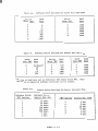
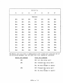
~able 4-4.
Soft·.rare Switch Set::in9s for Slave Port aaud Rate
Baud
Rate
Switch
Value
·ss· .
switch
~,a1ue
so
9
2
3
75
110
A
B
4
134
5
6
7
150
300
600
1200
l
a
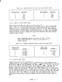
Table 4-5.
Switch
Value "SM"
0
1
2
3
4
Baud
Rate
·ss·
1800
2400
3600
4800
7200
9600
c
D
E
Software Switch Settings for Master Port eaud Rate
Baud
Rate
Switch
Value •sM"
Baud
Rate
Switch
Value "SM"
aaud
Rate
5
6
7
8
150
300
600
1200
1800
A
8
2400
3600
4800
7200
<l600
Hardware*
50
75
110
134
9
c
D
E
-----------------------------·-----------------------~ ----------~~~~~---1
*Defaults to baud rate set on Controller PCB rotary switch SWl.
applicable to Executive software revisions 11.0 and higher.
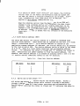
Table 4-6.
Software Switch
•so• Setting
1
2
3
4
5
6
7
8
only
Software Switch Settings for Control Delivery Time
Software Switch
Control Del. Time
msec.
msec.
msec.
msec.
msec.
msec.
sec.
2 sec.
10
30
70
130
250
500
1
6300A, o. 4-7
•so•
Settinq
9
A
B
c
D
E
F
Control Del. 't'ime
4 sec.
8 sec.
16 sei:.
30 sec.
1 mill.
2 min.
4 min.
4.2.3
4.2.3.1
?rogram Examoles
Local Input/Output
The following sample program shows the basic local input/output and logic
features of the non-vital ?roqram language:
PROGRAM NBR1;
INTERFACE
LOCAL
OUTPUT WORD:
OUT.1, OUT.2, OUT.3, OUT.4, OUT.S;
INPUT WORD:
IN.A, IN.B, IN.C;
BEGIN
ASSIGN IN.A AND IN.B
TO OUT.1;
ASSIGN IN.A XOR IN.B
TO OUT.2;
ASSIGN IN.A OR IN.B
TO OUT.3;
ASSIGN NOT IN.A
TO OUT.4;
ASSIGN IN.C
TO OUT.S;
END
The major sections of the program (PROGRAM, INTERFACE, LOCAL, OUTPOT WORD
etc.) are always placed in the order shown. These are discussed further in
section 4.2.4.
The INTERFACE section defines the local inputs and outputs, corresponding to
the r~lay-output and optical input boards, and individual bits on those
boards, in the cardfile. This sample program requires one LOCAL relay-output
board and one LOCAL optical-input board. The output board and input board
must be installed as follows:
GENISYS - Output board in slot Jl CJ3 of the cardfile) and input boar1 in
slot #2 (J4 of the cardfile).
MICROLOK PLUS - Output board in non-vital slot il CP of the cardfile) and
input board in non-vital slot #2 CO of the cardfile).
Five output bits (OUT.I, OUT.2, OUT.3, OOT.4, OUT.5) are defined on the output
boara. OUT.I is delivered on the first output (bit 0). OUT.2 through OUT.5
are delivered through bits 1 through 4, r~spectively. Three inputs are
similarly defined for inputs O through 2.
The number and order of the I/0 •boards• in the program text must match the
actual hardware configuration. Output board definitions must be specified
before input board definitions in the program. This is in accordance with the
left-to-right order of I/0 boards in the cardfile (see Figures 2-2 and 3-3).
Less than 16 bits may be defined on an input or output board. Unused input
bits are ignore~. Unused output bits are always output as zero.
6300A, p. 4-8
NOTE
The GENISYS Dev~lopment System compiler per~its up
to 16 I/0 PCBs to be defined. However, the MICROLOK
PLUS non-vital section only allows two I/0 PCBs.
When writing the application program for the MICROLOK
PLUS non-vital section, make certain not to specify
more than two I/0 boards. ~o error message will be
generated if more than two boards are specified.
The actual system logic is defined with ASSIGN statements. These statements
define the interconnecting logic of the inputs and outputs. The order of the
ASSIGN statements will usually have no effect on the logic (refer also to
section 4.2.5.2). In this example, OUT.I is the logical •ANo• of the two
inputs IN.A and IN.B. Similarly, OUT.2 is the ·EXCLUSIVE OR· and OUT.3 is the
•oR• of the two inputs. OUT.4 is the logical •NoT• of IN.A, and Otn'.S
directly follows IN.C.
4.2.3.2
Internal Relays and Stick Logic
The following program shows the handling of internal relays and stick logic:
PROGRAM NBR2;
INTERFACE
LOCAL
OUTPUT WORD:
OUT.1, OUT.2, OUT.3, OUT.4,
INPUT WORD:
IN.A, IN.B, IN.C. IN.D;
VAR
STICK;
BEGIN
ASSIGN IN.A AND IN.B
ASSIGN IN.A XOR IN.B
ASSIGN IN.A OR IN.B
ASSIGN NOT IN.A
ASSIGN IN.C
ASSIGN IN.C OR (STICK AND NOT IN.D}
ASSIGN STICK
END
OUT.5, OUT.6;
TO
TO
TO
TO
TO
TO
TO
OUT.1;
OUT.2;
OUT.3;
OUT.4;
OUT.5;
STICK;
OUT.6;
This program is similar to the program •NeR1• in section 4.2.3.1, however
OUT.6 is added as the 6th output on the relay-output board. Also, input IN.D,
is added as the 4th input bit. A new section VAR is added to define an
•internal bit•. An internal bit is neither input nor output, it is onl~
processed internally. All internal VAR bits are initially deenergize~. An
example is a stick relay. Note the additional ASSIGN statement:
ASSIGN IN.C OR (STICK AND NOT IN.O)
6300A, p. 4-9
TO
STICT:
Nhen input !N.c is energized, ST!Cl becomes energized. With the following
direct assignment of STICK to OUT.6, both OUT.6 and STICK will remain
energized, even if IN.C is deenergized. The internal STICK and OOT.6 :.rill
remain energized until IN.Dis energized. This results in the clearing of the
stick circuit. Note, however, that if IN.C is still energized, STICT and
OUT.6 will remain energized.
4.2.3.3
Timing Relays
The sample program below shows the handling of timing relays. This program
makes use of one timer relay. Continuing from the e~ample in section 4.2.3.2.
two more defined output bits, OUT.7 and OOT.8 are added. In the VAR section.
another internal relay c•T1•) is defined. Relays with timing characteristics
are defined in the TIMER section, always after the VAR section. Every bit
name specified in a TIMER statement must be previously defined as an output or
internal bit. Input bits may not have timing characteristics.
PROGRAM NBR3;
INTERFACE
LOCAL
OUTPUT WORD:
OUT.1, OUT.2, OUT.3, OUT.4,
INPUT WORD:
IN.A, IN.B, IN.C, IN.D;
VAR
STICK, T1;
TIMER
T1:
CLEAR
SET= 1:SEC
BEGIN
ASSIGN IN.A AND IN.8
ASSIGN IN.A XOR IN.8
ASSIGN IN.A OR IN.8
ASSIGN NOT IN.A
ASSIGN IN.C
ASSIGN IN.C OR (STICK AND NOT IN.D)
ASSIGN STICK
ASSIGN NOT T1
ASSIGN T1
ASSIGN NOT T1
END
OUT.5, OUT.6 OUT.7, OUT.8;
= 1:SEC
TO
TO
TO
TO
TO
TO
TO
TO
TO
TO
15300.i\, p. 4-10
OUT.1;
OUT.2;
OUT.3;
OUT.4;
OUT.S;
STICK;
OUT.6;
T1;
OUT.7;
OUT.8;
I
Note the ASSIGN statement:
ASSIGN NOT Tl
TO Tl;
The statement will take the current value of bit •Tl" (initially 0), perforn
the logical •NoT• operation, and attempt to assign a value of •1• to Tl.
nowever, because Tl is defined to have a SET or pick-up delay of 1 second, the
actual value will remain at O for one second. When time has elapsed and the
bit becomes a •1•, the assignment statement will execute again, causing the
value of •o• to be assigned to •T1• with a one second delay (as specified by
the CLEAR parameter of the timer statement). Thus, the internal bit, •T1•,
will toggle at a one second rate. Note the final two assignment statements
added to this program:
TO OOT 7:
TO OUT 8:
~SSIGN Tl
ASSIGN NOT Tl
Outputs OOT.7 and OOT.8 will alternately flash at a one second rate COUT.7 on
when Tl is •1• and OtJT.8 on when Tl is •o•).
4.2.3.4
Master/Slave conununications
The following program shows the handling of Master/Slave serial communications
for the Master unit:
PROGRAM NBR4M;
INTERFACE
LOCAL
INPUT WORD:
IN.A, IN.B, IN.C;
MASTER
AOORESS:2
OUTPUT:
M.OUT.1, M.OUT.2, M.OUT.3, M.OUT.4, M.OUT.5;
BEGIN
ASSIGN IN.A ANO IN.B
TO M.OUT.1;
ASSIGN IN.A XOR IN.8
TO M.OUT.2;
TO M.OUT.3;
ASSIGN IN.A OR IN.B
ASSIGN NOT IN.A
TO M.OUT.4;
TO M.OUT.S;
ASSIGN IN.C
ENO
6300A, p. 4-11
~his sample shows :~aster /Slav~ serial communications for the Slave unit:
PROGRAM NBR4S;
INTERFACE
LOCAL
OUTPUT WORD:
OUT.1. OUT.2, OUT.3;
SLAVE
AODRESS:2
INPUT:
M.IN.1. M.IN.2, M.IN.3, M.IN.4, M.IN.S;
BEGIN
ASSIGN M.IN.1 OR M.IN.S
ASSIGN M.IN.4 XOR NOT M.IN.2
ASSIGN M.IN.3 ANO M.IN.4
TO OUT.1;
TO OUT.2;
TO OUT.3;
ENO
The above programs allow communication between a Master and one Slave unit.
The Slave unit responds to address 2. The Master unit inputs three bits of
information, performs logic functions and sends five new output bits CM.OUT.l
through M.OUT.5) to the Slave unit. The Slave receives these bits (M.IN.l
through M.rN.S), performs additional logic and outputs the new computed values
to the relay-output PCB in the cardfile.
For a complete explanation of Master/Slave communications, refer to section
4 • 2 • 4 • 2 , pa rt c •
4.2.4
4.2.4.1
Detailed Statement Descriptions
•PROGRAM• Statement
The first statement in the program must be a PROGRAM statement. This
statement gives a name to the program for documentation purposes.
FORMAT:
PROGRAM
(id) ;
The identifier entered here will be printed in the listing at the top of the
symbol table. It is written with user-defined symbol (refer to section
4.2.1.3). Comments may be placed before a program statement.
6300A, p. 4-12
4.2.4.2
a.
·rNTERFAcE· Sec~ion
General
The INTERFACE section defines the various output and input specifications of
the system. There are three sub-sections in the INTERFACE section: LOCAL
I/0, MASTER I/0 port and SLAVE I/0 port. These corresoond to the three
input/output interfaces on the controller board. At least one of the three
I/0 interfaces must be defined. Each begins with a name (LOCAL, MASTER, or
SLAVE) that designates the type of interface. The LOCAL I/0 (if any) is
defined first, followed by MASTER Cif any) and then SLAVE (if any). Within
each of these, outputs Cif any) are defined first, followed by inputs (if
any). Either outputs or inputs may be blank, but not both at the same time.
The standard format is shown at the top of the next page.
b.
LOCAL I/0
The LOCAL r/o subsection defines the names of the bits that are input and
output on the cardfile I/0 boards. (If there is no local I/0, this subsection
may be omitted.)
GENISYS - Up to 16 words may be defined, with 1 to 16 bit names on each
word.
MICROLOK PLOS - One or two words may be defined, with 1 to 16 bit names on
each word.
Each input or output WORD corresponds to a single I/0 board. The first symbol
defined on each word corresponds to the first input or output on the
corresponding board. The second symbol corresponds to the second input or
output, and so on. On interfaces where there is an unused bit between two
active bits, the symbol SPARE must be used to indentify the unused bit. All
output boards must be fully defined ahead of input boards. Outputs or inputs
that are unused at the end of a control or indication word need not be defined.
NOTE
Input boards are scanned at a 50 millisecond rate. Control
Delivery times are selectable (compiler switch •so•, refer
to section 4.2.2.3).
~300A, p. 4-13
I
PROGRAM <id>;
INTERFACE
LOCAL
GENISYS•: Up to 16 total 110 boards. <id list>
OUTPUTWORD: <id list>;
may have up to 16 relay names.
MICROLOK PLUS™ (Non-Vital): One or two 1/0
boards. <id> list may have up to 16 names.
INPUTWORD: <id list>;
MASTER
ADDRESS: n
OUTPUT: <id list>;
INPUT: <id list>;
ADDRESS: n
OUTPUT: <id list>;
INPUT: <id list>;
Up to 255 addresses. <id list> should
correspond to its associated Slave unit
.--~~~~~~~------~~·--------.
SLAVE
ADDRESS: n
OUTPUT: <id list>;
INPUT: <id list>;
c.
(1)
---i
___J
Each <id list> should correspond to its
associated Master unit. Only 1 Slave
Serial Communications Interfaces
Master Port
The Master serial port (see Figure 4-1) enables a given GENISYS or MICROLOK
PLUS unit to communicate with another such Slave unit or units. The MASTER
subsection defines the I/0 operations for the Master unit of such a system.
For each Slave unit in this system, one ADDRESS ••• OUTPUT ••• INPUT group must b~
defined under the MASTER interface section of the program. The Master unit
communicates among the Slave units defined in a round-robin polling scan. The
order of the address statements in the program (not the address numbers)
represents the order in which Slave units will be polled. The scan time of
the Slav~ units varies, based on the total system configuration. This
includes baud rate and number of defined Slave units. The Master unit
delivers an out~ut bit to each Slave when the output bit changes value. ~ote
that the connection from a Master port is always made to a correspondingly
progr3mmed set of Slave ports. All addresses defined under the MAST~R
interface section must be in the range of 1-255 (Dis not valid). Each
address must also be unique.
6300A, p. 4-14
I
( 2)
Sla11e Port
~~e Slave interface on the GENISYS or ~ICROLOK PLUS unit is designed to
conununicate with only~ such protocol Master unit. In the SLAVE section of
t~e program, only one ADDRESS ••• OUTPUT ••• INPUT group may be soecifierl. (Each
unit ·= an only be a Slave to one Master unit, but can be a MasteC' to moC'e than
one Slave units}. Each Slave port only responds to its one, proper address.
Therefore, only one ADDRESS group is permitted. When defining the Slave port
address in the software, use a number other than zero. Otherwise, set this
value to zero and select the address with switch JS of the Controller board
(refer also to section 8.4). As with the other INTERFACE sections, all output
bits must be specified before any input bits.
(3)
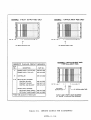
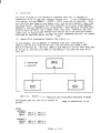
Master/Slave Programming Example (See Figure 4-1)
In this example, the tl GENISYS or MICROLOK PLUS unit receives two bits
CRCV.A.2 and RCV.B.2) from the t2 unit, and two more bits CRCV.A.3 and
RCV.B.3) from unit 13. Two bits {SND.A.2 and SND.B.21 are also sent from unit
tl to unit t2, and two bits CSND.A.3 and SND.B.31 are sent from unit tt to
unit t3.
MP
SP
= MASTER PORT
=
UNIT #1
(MASTER)
SLAVE PORT
MP
SP
SP
UNIT #2
(SLAVE)
UNIT #3
(SLAVE)
Figure 4-1.
Master/Slave Communications Programming Reference Diagram
The program code for unit 11 in Figure 4-1 (MASTER I/0 subsection) is as
follows:
MASTER
ADDRESS:2
OUTPOT:
INPUT:
SND.A.2, SND.9.2;
RCV.A.2, RCV.B.2:
ADDRESS: 3
OUTPUT:
INPOT:
SND.A.3, SND.B.3;
RCV.A.3, RCV.S.3;
6300A, p. 4-15
In the Slave units, :~e SLAVE subsections must hav~ ADDRESS ••• OUTP!JT ••• INPOT
listings that cor~esoond to the ~quivalent listing in the Master unit
?rogram. 3oth ?rograms in this example are similar, accepting two input bits
and sending two out?ut bits. The input and output bits in the Slave unit
programs need not use the same names as the corresponding bits defined in the
Master unit program. However, the input/cutout order must be correct: The
first bit on the Master unit's MASTER output list is the first bit on the
Slave unit's SLAVE input list, etc.
The program for the Slave section of unit t2 is as follows:
SLAVE
ADDRESS: 2
OUTPUT:
I NP UT:
OUT.2.A, OUT.2.B;
IN • 2. A, IN. 2 • a ;
The program for the Slave section of unit 13 is as follows:
SLAVE
ADDRESS: 3
OUTPUT:
INPUT:
OUT.3.A, OUT.3.B;
IN • 3 • A, IN • 3 • a :
In this example, the Master unit (refer to program segment on previous page)
outputs •sND.A.2• and •sND.s.2• to Slave unit t2, where they are input into
the relays •rN.2.A• and •rN.2.s•, respectively. Onit #2 outputs •ooT.2.A• and
•oUT.2.s•, which are received by the Master unit as •Rcv.A.2• and •Rcv.a.2•.
The I/0 for unit 43 is similar.
NOTES:
A single GENISYS OR MICROLOK PLUS unit may be program-
mmed to use both its Master and Slave ports
simultaneously.
Two or more units programmed to be Slaves of some Master
cannot conduct direct serial communication with each
other. Any communication between Slave units must pass
through their common Master unit.
4.2.4.3
•vAR• Section
The VAR section of the GENISYS program is used to specify the names of
internal relays (those that are neither input or output). Relays not defined
in the VAR section must be defined as an input or output on a MASTER, SLAVE
LOCAL interface. The format of the VAR section is as follows:
VAR
( id list)
.
,
Eac:1 ident i fi~ r in the
( id list)
is separated by a comma.
6300A, p. 4-16
4.2.4.4
•TIMER" Section
NOTE
Refer to section 5.2 for a detailed description of
system internal timing.
The TIMER section of a program is used to give distinct set (pick) or clea~
(drop) delays to an internal relay or output bit. A bit not specified in a
TIMER statement will, in effect, set or clear instantaneously.
Timer delays
can be individually specified in the program. The available units inclune:
1.
MIN (minutes)
SEC (seconds}
2.
3.
MSEC (milliseconds)
Generally speaking, the smaller units have greater timing accuracy:
Onit
Accuracy
MIN
C+/-3sec.)
(+/- 50 111sec.)
( +/- 5 lff9eC. >
SEC
MSEC
The shortest non-zero delay allowed is 10 milliseconds; and the longest is 25
minutes. The actual ranges that the compiler uses are as follows:
Oni t
Range*
MIN
0.1 min. to 25 min.
0.1 sec. to 25 sec.
10 msec. to 2500 msec.
SEC
MSEC
*NOTE
Although the lowest timing ranges (or minutes and
seconds are given as 0.1 min. and O.I sec., respectively, the actual set and clear times specified
must be an integer value. For example, 0.1 sec. would
be specified as 100 msec., and 0.1 min. as 6 sec.
Values greater than the above may be used. The compiler will automatically
convert out-of-range values to the smallest acceptable range. For example, if
3000 MSEC is entered, the compiler will convert this to 3:SEC (with an
accuracy of +/-50 milliseconds). However, small values with larger units will
not be converted to the smallest units, even if this is possible. For
example, if 2 :SEC is entered, the compiler will read this as 2 second_s, and
not convert this to 2000:MSEC.
The standard format for entering timer values is as follows:
TIMER
( id list)
{ id list)
SET =
SET=
(integer)
(integer)
(unit)
(unit}
6300A, p. 4-1 7
CLEAR = ( integer)
CLEAR = (integer}
(unit)
(unit)
..
•
•
I
;.Jhe re:
( id list) is a list of previously defined internal or output r:elay bit
names separated by commas.
(integer) , is an integer constant in the range of O - 9999
(unit)
is specified as one of the Reserved Words:
1.
2.
3.
MSEC - for milliseconds
SEC - for seconds
MIN - for minutes
For example:
TIMER
Tl, T2:
lXXRR:
4.2.4.5
SET= 500:MSEC
SET=- 250:SEC
CLEAR
CLEAR
2
500:MSEC;
= 0 :MSEC:
Main Program Body
The actual system logic is written in the main program body. Every internal
or output relay bit name defined in the INTERFACE and VAR sections should be
gi•1en a value in the main program body (except •spare• (keyword) bits). This
is done by making the bit the object of an ASSIGN statement (refer to section
4.2.4.6). If an output bit is not the object of an ASSIGN statement, the
program may operate properly, but that bit will be ignored. Serial input bits
(from Master or Slave) may be the object of an ASSIGN statement. For a
complete explanation of how the actual input/logic/output cycle occurs in
r:elation to input assignments, refer to section 4.2.5 (Run Time System
Description l.
4.2.4.6
ASSIGN Statement
The ASSIGN statement enables the var:ious Boolean operators (OR, NOT etc.) and
bit names to be combined in logic equations. ?or example:
ASSIGN IN.A
TO OUT.S;
XOR
IN.C
AND
(NOT IN.A
OR
IN.B)
Four logical operators ar:e available to create expressions in a program.
These are listed in Table 4-7:
Table 4-7.
eserved
Word
Shorthand
Operator
Logical Operator symbols
Reserved
Word
Shorthand
Operator
OR
+
NOT
AND
XOR
*
6300A, p. 4-18
Sither for:n <Reser •,ed :.Tard or shorthand operator character) may be used in
assignment ex?ressions. For e~ample, the ASSIGN statement shown on the
pre•,ious page :nay be ·..iritten using shorthand symbols:
ASSIGN
TN .A ·
IN .C
@
*
IN .Bl
+
("" IN.A
TO OUT.5~
The operators AND, OR, NOT and XOR, along with their shorthand symbols, are
evaluated according to the truth tables in Table 4-8:
Table 4-8.
ASSIGN Operators Truth Tables
Inputs
A
B
AND
A * B
0
0
l
1
0
1
0
1
0
0
0
1
OR
A+
XOR
A @
B
c
V"\
0
1
1
0
0
1
1
1
NOT
A """'a
1
l
l
0
0
l
0
0
The order of evaluation is determined by the following precedence rules:
HIGHEST:
LOWEST:
NOT
AND
OR
XOR
Operations with the highest precedence are performed first. Operations at the
same precedence level are evaluated left to right. Parentheses may be added
to alter this default order. Parentheses take precedence over the defined
operational order. The order of evaluation of the above assignment statement
is shown in Figure 4-2:
ASSIGN
IN.A
XOR
IN.C
AND
(NOT
IN.A
L,_J
L2
3
I
4
j
OR
I
IN.8)
(A
OR
A
B)
j
AND
L,_J
L2
... OUT.S
Figure 4-2.
L
TOOUT.5
OR
B
ANO
c
L,_l
2_J
c
ASSIGN Operators, Order of Precedence Samples
If more than one relay is to be assigned the same value, the logic expression
need not be repeated in a second ASSIGN statement. Additional relay names may
be assigned using the same statement by listing them after the •To• Reser~ed
Word, separated by conunas. For example:
ASSIGN A AND B OR NOT C
TO D,E,?;
6300A, p. 4-19
4.2.S
4.2.5.1
~un Time System D~scription
Inout/Outout Desc~iption
The GENISYS and MICROLOK PLUS (non-vital section) svstems use an internal ~AM
table containing the current state of every relay defined in the svstem. This
table includes the LOCAL input and output bits, as well as the internal bits
defined in the VAR section.
The values of LOCAL input bits in the table are automatically updated in a SO
millisecond scan. Therefore, LOCAL inputs may not receive a value based on an
ASSIGN statement, otherwise a logical conflict could exist. For example,
there could be an input with an actual state of •1•, and a logic ASSIGN
statement which computes its value as •o•.
The LOCAL output bits are delivered in groups of 16 whenever any one of the
bits in that group change state. If Constant Delivery relay-output boards
CN451441-7101) are used, the outputs directly follow the states of the
internal table.
Input bits on either the Master or Slave serial line have their internal table
value updated differently. When a GENISYS or MICROLOK PLUS unit receives a
bit on a serial line, its received value is put in a table. rt will keep that
value until the bit is received again. Because the input value of serial bits
is only updated when received, each may also be given a value with an ASSIGN
statement. However, no more than one ASSIGN statement may be specified for
each relay.
(The slot off of a signal request application illustrates a serial input bit
being given a value from an ASSIGN statement. The controlling Master unit,
which may be a Eull office mini-computer, may send a green request using a
serial input bit. This request may be combined with other information to
produce the actual green output. The green signal request is usually to be
cancelled when the appropriate track circuit becomes occupie~. Note that
logic may be written to clear the signal request input from the serial line.l
4.2.S.2
Logic Processing
Note
Refer to section 5.4 for a detailed descriotion of
logic processing and queuing.
An ASSIGN statement is equivalent to tracing the path or paths of current flow
from a battery to the assigned relay coils. Therefore, the logic for all of
the wiring associated with that relay coil must be contained in one ASSIGN
statement. The order of the ASSIGN statements in the source program will
usually have no effect on the output.
An ASSIGN statement is re-computed each time one of the relay coils included
in the statement changes state. This involves the following chain of events:
The system first determines if the coil has a timing delay. If so, the
specified time is run until the relay is to be set or cleared. Assignments
for non-timer coils ar~ carried out inunediately, and all ASSIGN statements in
6300A, p. 4-20
I
which this ~oil is referenced are re-computed. This process continues until
the system reaches a stable state. During the ti~e ASSIGN statements are
~eing computed, no out~ut operations (local or serial) are performed; inputs
are still scanned at SO millisecond rate. ~ny output started before the logi~
sequence will continue to be processed. However, outputs cannot be updaten.
In accordance with actual relay-logic practices, logic processing always uses
a break-before-make format: When a relay changes values, the break is done
before the make. However, there are circumstances where a make may occur
before a break in a relay chain, depending upon the setting of the queueing
.. compiler switch %$Qv'\ (v = + or -). The relay execution order in Figure 4-l
shows the operation of this switch option:
EQ1
EQS
EQ3
Q+ ORDER
!!!M
1. EQ1
2.EQ3
3.EQ6
R3
M!!f.
t
EQ2
Figure 4-3.
t
t
EQ4
EQ6
0- ORDER
1. EQ1
2.EQ2
3.EQ3
4. £()4
5. £06
6. EQS
4. EQ2
5. EQ4
6.EQS
Queuing Option Reference Diagram
When the switch is set to Q- (default), equations are processed relay by
relay, with breaks executed before makes in the order in which they occur. !n
Figure 4-3, if relay Rl changes state, EOl is executed (break), followed by
EQ2 (make}. Next, the change in EQl (relay R2) causes EQ3 to be executed
(break), thus the make of EQ2 occ~rs b~fore the break of EQ3.
If the queuing switch is set to Q+, there are two queues for logic equations,
including one for the breaks and one for the makes. Breaks are always done
first, regardless of when they happen. In Figure 4-3, note that the three
break equations CEQl, EQ3, EQ6) are executed before any of the makes. Even ir
the makes were queued first and then break occurred, the break is done first.
NOTE
The following paragraph applies to GENISYS Development
System versions 3.0 and higher:
In versions of the compiler before 3.0, the Break-Before-Make rule was not
always followed when processing some types of logic equations. Under certain
limited conditions, logic equations could be executed in an order that woula
not strictly follow the Break-Before-Make ordering. Version 3.00 is designed
to 3ssure that all equations will be properly processeo and executed in the
Break-Before-Make order.
If an older application logic program is recompiled with version 3.00, the
EPROMs generated may not be identical to the older EPROMs. These differences
would only involve the order in which the logic equations are processed. No
changes are required on any installation that is currently in service and has
undergone complete testing during a cut-over.
6300A, p. 4-21
I
NOTE
The following paragraph appli~s to GENISYS Development System 1ler3ions 1.03 and higher, and Executive
PROM IC29 Revisions 3 and higher.
In earlier Versions
and Revisions, a maximum of 500 equations may be queued
at any one time. If the 2-queue option (Q+l is used, a
maximum of 250 equations may be present on each queue
(break and maice).
maximum of 1000 equations may be queued at any one time. If the 2-queue
option (Q+) is used, a maximum of 500 equations may be present on each queue
(break and make). Any attempt to queue more equations, using either option,
will be ignored by the Run Time e~ecutive. The Q- option is slightly faster
and should be used when possible. However, it may cause problems with some
stick circuits (consult US&S Engineering).
A
4.2.5.3
Serial Communications - Pre-Defined Relays
When the serial I/0 lines (Master or Slave) are used in GENISYS or MICROLOK
PLOS, it may be necessary to condition logic processing for successful or
unsuccessful completion of communications Ci.e. code line up or down). Par
example:
1.
A Master unit may be programmed to turn on an output Ci.e. an indicator
lamp) when it loses communications with a Slave unit.
2.
A Slave unit may be programmed to perform field •auto-clear• functions if
communications are lost with its Master unit.
Both of these situations can be accommodated with the GENISYS or MICROtOK PLOS
(non-vital) system. The compiler contains pre-defined relay names that are
SET and CLEARed automatically by the Run Time system.
On the Master Port, one internal relay is created for each Slave unit address
specified in the MASTER part of the INTERFACE section. Each name is
automatically defined as follows:
SLAVE.ON.n
The letter •n• corresponds to the address of the particular Slave unit served
by the relay. The value of •n• may range from 1 to 255, the same range as
Slave unit addresses.
These relays may be used as part of an expression in an ASSIGN statement to
condition logic, or may be listed in an output statement. Since they have a
predetermined value, they may not appear in an input statement, or be the
object of an ASSIGN statement.~Ini~ially, these relays are clear (dropped). When the first valid message is
received from a Slave unit, the associated relay in the Master is SET
(picked). The relay will remain SET until the Master detects two consecutive
errors in transmission. ~t this time, the relay is cleared Cdroµped) and will
remain in this state until communications are resumed with that Slav~.
6300A, p. 4-22
At each Slave unit, one internal communication relay is automatically defined
as:
MASTER.ON
This relay is automatically SET and CLEARED by the Run Time system
the status of communications from the Master unit. It may be used
an expression in an ASSIGN statement to condition logic, or may be
an output statement. Since it has a pre-defined value, it may not
an input statement, or be the object of an ASSIGN statement.
to indicate
as part of
listed in
appear in
The MASTER.ON internal relay is SET and CLEARED differently from the
SLAVE.ON.n relays. MASTER.ON is initially CLEAR (dropped). When the Slave
unit receives the first valid message addressed to its station number, the bit
is set. The Slave unit then continues to look for the text header, followed
by a trailer, followed by text header, etc. If more than five seconds elapses
after receiving Cl) a header with no trailer, or {2) a trailer without a new
message that starts with a header, the bit is cleared.
4.2.5.4
Valid Bit Option - Introduction
NOTE
Refer to section 5.3 for a detailed description of
the Valid Bit Option.
At power-on reset, the GENISYS or MICROLOK PLUS (non-vital) unit sets all
internal and output relays to zero (clear). No actual output can occur at
this time. After the initial reset, optical-input boards (if any) are scanned
to determine the value of bits defined as LOCAL INPUT bits in the program. Ir
any input bits are defined in the program, but refer to boards not actually in
the cardfile, those bits will be given •rnvalid• or unknown values.
Similarly, any bit defined as an input on either of the two serial lines
becomes •invalid• until the bi~ is received from the unit at the other end of
the line.
During processing of an ASSIGN statement, any •invalid• input bit referenced
during the computation will stop the processing procedure. The relay defined
as the object of this ASSIGN statement cannot be changed. Only •invalid•
input bits will stop the processing of a logic statement.
Output and internal bits may also be •invalid•, but will not interrupt the
completion of an ASSIGN statement. At reset, these types of bits are
initialized as zeros. ~hey are treated as valid zeros during processing of
ASSIGN statements. Once all output bits in a tOCAL output word or serial
protocol byte become valid, the LOCAL word is delivered to the actual outputs,
or it becomes available to the serial line. However, the bits cannot be
delivered until they have received a •valid• value as the result of
successfully resolving an ASSIGN statement.
6300A, p. 4-23
NOT!::
The following statement applies to GENISYS Development
system Versions 1.02 and higher. In Versions 1.00 and
1.01, the indicated Boolean identities would not be
evaluated.
The following Boolean identities will be evaluated even if x has an •invalid•
value:
l
OR
x
=
OANDx:oO
1
In these identities, the value of xis irrelevant.
1, and O ANDed with anything is a O.
4.2.6
1
ORed with anything is a
Relay Models and Programming Techniques
Figure 4-4 provides sample relay circuits Ear GENISYS and MICROLOK PLUS
(non-vital) programming models. The flasher relay set-up could not exist in
actual relay logic, but is possible in GENISYS or MICROLOK PLUS by
establishing a distinct pick-up/drop-away interval for the relay. The
pertinent parts of the program include:
Tl:
CLEAR=l:SEC;
SET=l :SEC
ASSIGN
NOT
TO Tl;
Tl
ASSIGN NOT T1 TO T1
T1
SN
SB = SOFTWARE "BATTERY'"
SN
SOFTWARE "NEGATIVE"
=
---SB
ASSIGN IN. 1 AND NOT CANCEL TO IN. 1
CASCADING TIMERS
SERIAL INPUT CONTROL
SB----
T1
(X-SECOND DELAY)
1-----------------SN
I
(X-SECOND
DELAY)
I
-----------~
IN.1
I
T2
1--------- SN
SN
CANCEL
OUT.1
I
SN
~
LsB
Figur~ 4-4.
NET DELAY: X + X AT OUT.1
conceptual Relay Models for GENISYS and MICROLOX PLUS Programming
6300A, p. 4-24
If the timer value is.not specified, the •contact• will operate at a speed
which cannot be detected by the :un time system. This would create an
indeterminate func~ion at this point, inhibiting execution of the program.
The double coil relay examples in Pigure 4-4 are conceptual models which
pertain to signal control slotting. Models can not apply to circuits with
control contacts to both coils of a double-coil relay. The pertinent program
statement for the model containing the CANCEL contact is:
ASSIGN NOT CANCEL AND IN.l
TO IN.l;
The capability to assign to serial inputs may be applied to the design or auto
clearing controls. In the case of auto clearing of requests, if the input is
a request for a clear signal and CANCEL is a track relay, the signal request
will be cleared when the track is occupied.
The following statement shows how requests from the office can be cleared if
the communications link is lost:
ASSIGN MASTER.ON AND IN.l
TO IN.l:
(These techniques are presented as conveniences for designing auto clearing
logic. They may not be suitable in all applications. Consult OS&S
Engineering for further guidance in the development of this type of logic.)
Cascading timer relays are used to build up a comparatively long delay on the
output delay relay. Only one timing specification (SET and CLEAR) needs ta be
written for all timer relays (equal addends for the desired delay):
Tl, T2:
SET=S:SEC
CLEAR=S:SEC
6300A, p. 4-25
I
4.3
GENISYS DEVELOPMENT SYSTEM (G.O.S) - GENERAL
The GENISYS Development System CG.D.S) enabl~s the user to compose, aebuq and
load an application program into the GENISYS or MICROLOK ?LOS (non-vital
section) system hardware. Refer to Appendix A for development system
components. (Note: A text editor is not available with develocment system.)
Figure 4-5 shows the general steps in the use of the G.D.S. The source
program is written and entered into the compiler using a text editor. The
compiler checks the program for proper terminology and format and lists any
errors in a listing file. Using the information in this file, the user
returns to the text editor and corrects these errors. The compiler cannot
detect mistakes in the user's application of logic statements. These are
located using the Simulator. Again, the user returns to the text editor to
correct errors. When the simulator indicates satisfactory operation of the
program, it may be loaded into the Controller PCB EPROM. The compiler is used
to convert the source program into PROM tables. The EPROM programmer unit
performs final checks of these tables and the EPROM itself, before actual
loading of the data into the chip.
Figure 4-5.
4.4
Development System Block Diagram
G.o.s. - AVAILABLE FILES
The GENISYS Development System software uses seven file extensions. These
extensions enable the user to employ the various parts of the G.D.S:
Extension
File Contents
.GEN
source program for the application logic
• GLS
Listing file with errors produced by the compiler •
• GID
Identifiers Eile produced by compiler and used by simulat~r •
.C'iCD
EPROM code file produced by the compiler/assembler and used by
the simulator and EPROM programmer.
.GEQ
Equations generated by the simulator
• GSI
Simulator initialization file •
• GI~
Temporary file used during compilation •
6300A, p. 4-26
I
4.5
G.D.S. - COMPILER
NOTE
Different revisions of the GENISYS Development System
compiler may yield different check sums and code sizes.
However, the program should behave in the same manner.
The compiler checks and converts the application program into a code that can
be processed by the Executive software (contained in a separate Controller PCB
EPROM). The compiler performs two functions, including code generation and
assembling.
The code generation section checks the source program for any errors, using a
two-phase process: Syntax Analysis and Semantic Analysis. Syntax analysis
looks for improper •grammar• in the program. During this analysis, two types
of errors may be detected, including token errors (more than 12 characters,
illegal character, etc.) and statement syntax errors Cno BEGIN Reserved Word.
missing semicolon, etc.).
Semantic analysis checks for meaningful statements.
ASSIGN A AND B
For example:
TO<:;
If c is defined as an input bit, or a has not been defined, a semantic erro~
will be detected. Refer to sections 8.1 and 8.2 for a complete listing af
compiler error messages.
As the source program is processed, it is converted to a special-purpose code
that, in turn, is processed by the Assembler section of the compiler. The
assembler converts the output of the code generator to a format that can be
processed by the EPROM Programmer.
The compiler is accessed by using the batch file: GENISYS •name•. Typing in
this teem invokes the batch file. This file can perform several functions.
depending on how it is invoked:
GENISYS
name
GENISYS HELP
-rf (name) .GEN appears as a file in the current directory.
it is compiled. Otherwise, a •file does not exist• message
is di sp 1 ay ed •
-This displays the G.D.S. help file.
the top of the next page.
This file is shown at
The batch file performs several operations:
1.
2.
3.
4.
Determines if the requested file exists; displays error message and stops
if this file does not exist.
Deletes the previous EPROM code (.GCD) file
Calls the code generator
Calls the assembler if no errors were detectea.
The batch file is recommended for compiling a GENISYS or MICROLOK PLUS
non-vital program.
6300A, p. 4-27
GENISYS Help File
Version 3.00
1.
GENISYS Compiler
GENISYS name
For Help:
GENISYS help
Run the GENISYS compiler using the files:
name.GEN
(input)
Source file
name.GLS
(output source listing)
Listing file
(output for simulator)
name.GID
Symbol file
name.Geo
(ouput for PROM programmer)
PROM file
2.
Program PROMs
GENPROM
Program PROMs using the file name.Geo
3.
GENISYS Simulator
GEN SIM
Simulate the execution of a GENISYS program.
4.
GENISYS PROM Size Estimate
GENSIZE
For Documentation:
GENSIZE help
Estimate the size of a GENISYS program.
NOTE
HELP FILE ALSO APPLIES TO MICROLOK PLUS™, NON-VITAL SECTION
4.6
4.6.l
G.o.s. - SIMULATOR
General
The GENISYS Simulator allows testing of a completed GEN!SYS or MICROLOK PLUS
non-vital program, prior to actual loading into the system hardware. Commands
are provided in the simulator to mimic operating aspects of the designed
system. This includes setting and clearing internal and external relays,
executing logic equations, and advancing system time. Logic statements and
the system clock can be stepped individually, or simultaneously at any desired
increment. Commands are also available to display: (a) inputs and outputs
according to their actual arrangement in the system cardfile, (bl names, bit
numbers and status of individual relays, (cl logic statements as they are
executed.
With the simulator, the source program is compiled in the same manner as the
program that will be loaded into the system hardware, with the exception of
the debug switch (refer to section 4.6.2). The EPROM code file, with
extension .GCD, is the standard input to the simulator. The identifier symbol
file, with extension .GID, supplies relay names: without this file, the
simulator cannot be run. In the simulator, logic execution follows the same
dlogrithm as the Run Time system (refer to section 4.2.5.4).
6300A, p. 4-28
The simulator supports the following two switches:
switch
~ame
Comments
$Q
Queuing Option
If SQ+, use two queues (break before make),
othe~Nise use only one queue. (Default is 0-r
one queue.)
iv
Validation Check
If SV+, INVALID becomes a valid stater and is
checked during execution of logic equations. If
an equation contains an invalid bit, it will be
executed per the rules in section 4.2.5.4. If
SV-, all bits are cleared. (Default is V+r
validation on.)
4.6.2
4.6.2.1
Access to Simulator
General
NOTE
The following paragraph applies to GENISYS Development System Versions 1.01 and higher. Refer to
section 4.2.2.3, page 4-6, for the debug switch userl
in Version 1.00.
The simulator uses the EPROM file produced by the compiler. If a program is
to be debugged using the simulator, it must be compiled with the debug swit~a
~(%SD+'). The program does not have to be recompiled with %SD-\ to permit
programming of PROMs. The default is %SD-\.
Command terms in the following text are shown in all capital lettersr to help
distinguish them from other words in the text. In the acutual use of the
simulator, these words may be typed in lower case letters as well as upper
case. (CR) indicates the carriage return key (or ENTER).
4.~.2.2
Procedure
NOTE
In GENISYS Develpment System Versions 1.02 and higher,
the user can enter the simulator as •GENSrM• or
•GENSIM (file) •. The latter option allows the file
name to be obtained from the command line, without
being prompted.
1.
The simulator is run by entering GENSIM and a carriage return C {CR)), as
shown in the Help File. The simulator cover screen will then be
displayed, showing the version of the simulator.
2.
The prompt on the cover screen asks for the name of the source program.
When the name is entered, a tabulation will appear immediately below.
This table lists the basic totals of bits and boards in the source program.
6300A, p. 4-29
I
3.
Ent:y of the program name Nill also produce several permanent •status•
l:nes near the bottom of the sc:een. These lines are explained in section
4.6.3. To obtain a summary of all simulator commands, enter HELP (CR) at
the command prompt in the second status line. The Help Screen is
explained in section 4.6.4.3.
NOTE
The examples shown use programs compiled with the Validation
Option on ( %$V+ \ ) • This initially flags all bi ts as invalid.
4.6.3
Standard Formats
A typical set of status lines for the begining of a simulator exercise is
shown below:
Trigger List:
command-
10
system Time: 00:00:00:000
Program: NBR3
Timer List:
Screen: Init
0
The •Trigger List• refers to the total number of logic equations that are
queued to be executed. Whenever a bit changes, all logic equations that use
that bit will be placed on the Trigger List.
The •system Time• records the total time elapsed during the execution of
simulation. Left to right, increments are in hours: minutes: seconds:
milliseconds. All timed operations are advanced in increments of tens of
milliseconds.
The •Timer List" provides the total number of timer relays in the sour,::e
program that are on a timer queue.
Command names and lists of items such as relays are entered after the
•command" prompt, and executed with a carriage return (CR). When entering a
series of non-consecutive items after the conunand, leave a space between each
item number (i.e. l 3 7 12 19).
When entering a series of consecutive items,
a dash may be used for the intermediate items (i.e. 1-5 7-9 11-30). Ose the
same procedure when listing items by name Ci.~. OUT.1-0UT.3 OUT.S). If more
items are requested than are available in the listing, an •invali~ range•
error listing will appear. Do not attempt to enter more items than space
allows between •command• and •program•. Instead, enter a (CR) after the
first group and repeat the command to enter a following group.
"?rogram• indicates the name of the source program undergoing the simulation.
·s~reen• indicates the type of information presently on the screen.
example, the initial GENSIM cover screen is •rnit".
For
Scrolled information is run in the space immediately below the status lines.
For example, selected commands show source program logic equations and output
results in this area, as the program is executed. This section shows a
ma:<imum of four lines at one time. To scroll in format ion from the top of the
screen, enter NO (CR). This is the command for •No Display•. The status
lines will remain on the screen.
6300A, p. 4-30
I
4.6.4
Simulator Ooeration
4.6.4.l
General
When the simulator is executed and the EPROM tables are entered, the simulata~
performs the "fiecessary housekeeping functions:
(a)
Initialize all bits (either CLEAR OR INVALID)
Cb)
Reset system time
Cc)
Initialize all queues and lists
Cd)
Queue all equations on the Trigger List
4.6.4.2
Sample Program
Simulator conunands are described in subsequent sections, using a sample
program shown on page 4-32. Each of the available commands (see Help screen,
section 4.6.4.3) is exercised with this program in a typical order of
execution, and not in order shown on the Help screen. This is not a required
order; with practice, the user will find it desirable to call up a variety of
commands at any point in the simulation.
NOTES
Note the MICROLOK PLUS LOCAL I/0 assignments at the
bottom of the sample program. This shows the 2-board
limit placed on the MICROLOK PLUS non-vital section.
(Compare this with the GENISYS sample program, which
covers four total I/0 boards.) Otherwise, the complete MICROLOK PLUS sample program is identical to the
GENISYS program, except for the left-hand line numbering.
Certain aspects of the Simulator's operation, such
as scrolling lines, cannot be depicted in this te~t.
To best understand the operation of the Simulator, the
user should enter the sample program in his system
and run the various commands as they ar~ presented.
The card slot locations of the inputs and outputs are shown in the symbol
tables on page 4-33 (GENISYS) and 4-34 (MICROLOK ?LOS).
NOTE
As indicated in the MICROLOK PLUS diagram, board
slot numbers are based on the GENISYS cardfile slot
numbering. Make certain to note the difference in
the MICROLOK PLUS non-vital section slot numbering.
6300A, p. 4-31
GENISYs· PROGRAM
Gi:NISYS Source Listing
Copyright 1984,
,
THIS IS AN EXAMPLE
OF A BASIC NON-VITAL
PROGRAM.
3
4
r
4
TOTAL
1/0
BOARDS
Page:
%
2
5
6
7
8
9
5-JUN-1991
[ Version 3.00 I
Revised 1991,
Union Switch & Signal Inc.
\
%SD+
%SQ+
DEBUG ON\
TWO QUEUE OPTION\
10
1l
12
13
14
15
16
17
18
19
20
21
PROGRAM NBR3;
INTERFACE
LOCAL
22
TIMER
OUTPUT WORD:
OUTPUT WORD:
INPUT WORD:
INPUT WORD:
OUT. l, OUT.2, OUT.3,
SPARE, SPARE, SPARE, SPARE, SPARE.
OUT.4, OUT.S, OUT.6;
OUT.7, OUT.8;
IN.A, IN.B;
IN.C, IN.O;
SET= 1:SEC
SET= 1:SEC
SET= O:SEC
CLEAR= 1 :SEC;
CLEAR= 1:SEC;
CLEAR= 500:MSEC;
VAR STICK, Tl;
T1:
OUT.7:
OUT.8:
23
24
25
26
27
28
29
30
31
32
33
34
35
36
37
BEGIN
ASSIGN
ASSIGN
ASSIGN
ASSIGN
ASSIGN
ASSIGN
ASSIGN
ASSIGN
ASSIGN
IN.A ANO IN.B
IN.A XOR IN.B
IN.A OR IN.B
NOT IN.A
IN.C OR (STICK AND NOT IN.D)
STICK
NOT T1
T1
NOT T1
TO
TO
TO
TO
TO
TO
TO
TO
TO
OUT. t;
OUT.2;
OUT.3;
OUT.4;
STICK;
OUT.6;
T1;
OUT.7;
OUT.8;
END
Errors Detected:
0
LOCAL 1/0 SECTION OF MICROLOK PLUSrM NON-VITAL PROGRAM
.: --- TOTAL
2
{
· 110
BOARDS
12
13
14
15
16
LOCAL
OUTPUT WORD:
INPUT WORD:
OUT. l, OUT.2, OUT.3,
Sr .:.RE, SPARE, SPARE, SPARE, SPARE,
OUT.4, OUT.5, OUT.6, OUT.7, OUT.8;
IN.A, IN.B, IN.C, IN.0;
6 JOO.", p. 4-32
NOTES
GENISYs·
SYMBOL
TABLE
The sample bit symbol table below applies to GENISYs• Development
System Versions 1.01 and higher. In Version 1.00, the .. BIT TYPE• column is
placed in a separate column at the right and the ·rtMER• column is called
"TIME DELAY".
The Version 1.00 table as a whole covers 132 spaces; in Versions t.01 and
higher, the table covers 80 spaces.
In the ··swtTCH SETTINGS .. listing at the bottom, Version T.00 does nat
include #Polling Time Out• and the "Security" switch is "ON• or .. OFF•.
rather than .. ON" or .. AUTOMATIC-.
Bit Symbol Table for "NBR3"
IDENTIFIER
4
TOTAL
~:
1/0
'
BOARDS
LOCAL 1/0 BOARDS
OUTPUT - SLOT 3
OUT.1
OUT.2
OUT.3
SPARE
SPARE
SPARE
SPARE
SPARE
OUT.4
OUT.5
OUT.6
OUTPUT - SLOT 4
OUT.7
OUT.8
INPUT - SLOT 5
IN.A
IN.B
INPUT - SLOT 6
IN.C
IN.D
LOCAL VARS
STICK
Tl
5-JUNE-1991
SET
CLEAR
1.0: SEC
0.0: MSEC
t.O: SEC
500.0: MSEC
OUTPUT
OUTPUT
OUTPUT
5
6
7
8
9
10
11
OUTPUT
UNASSIGNED
OUTPUT
12
13
OUTPUT
OUTPUT
14
15
INPUT
INPUT
16
17
INPUT
INPUT
18
19
INTERNAL
INTERNAL
SWITCH SETIINGS
Slave Baud Rate
Master Baud Rate
Polling Time Out
Control Delivery Time
Security
Debug
Symbol Table Listing
Validity Check
Two Queue Option
TIMER
BIT NUMBER & TYPE
1
2
3
4
PAGE SYM- 1
Hardware switch
1200 BPS
1000 MSEC
Hardware switch
Automatic
ON
ON
ON
ON
6300A, p. 4-33
1.0: SEC
1.0: SEC
I
MICROLOK PLUS""'
SYMBOL TABLE
Bit Symbol Table for "NBR3'"
IDENTIFIER
r
2
TOTAL
1/0
BOARDS
S-JUNE-1991
BIT NUMBER & TYPE
LOCAL 1/0 BOARDS
OUTPUT • SLOT 3
OUT.1
OUT.2
OUT.3
SPARE
SPARE
SPARE
SPARE
SPARE
OUT.4
OUT.S
OUT.6
OUT.7
OUT.8
INPUT • SLOT 5
IN.A
IN.B
IN.C
IN.O
1
2
3
4
5
PAGE SYMTIMER
SET
CLEAR
1.0: SEC
0.0: MSEC
1.0: SEC
500.0: MSEC
OUTPUT
OUTPUT
OUTPUT
6
7
8
9
10
11
12
13
OUTPUT
UNASSIGNED
OUTPUT
OUTPUT
OUTPUT
14
15
16
17
INPUT
INPUT
INPUT
INPUT
18
19
INTERNAL
INTERNAL
LOCAL VARS
STICK
Tl
1.0: SEC
SWITCH SETIINGS
Slave Baud Rate
Master Baud Rate
Polling Time Out
Control Delivery Time
Security
Debug
Symbol Table Listing
Validity Check
Two Queue Option
Hardware switch
1200 BPS
1000 MSEC
Hardware switch
Automatic
ON
ON
ON
ON
NOTE
··ouTPUT • SLOT 3'" is slot .. p .. in the MICROLOK PLUS™ cardfile.
··1NPUT • SLOT 4• is slot .. Q" in the MICROLOK PLUS™ cardfile.
6300A, p. 4-34
1.0: SEC
I
4.~.4.3
~elp sc"een
HELP (CR) ?roduces the standard Simulator Help sc~een shown below. T,is
sc~een shows all display and operating commands, ano their purooses. Note
that the command names include capital and lower case letters. The capital
letters are the minimum characters required for a valio command. Osing the
QUIT command as an example, Q (CR) would cause an error message, but QO (CR)
would be a valid command. (QUI and QUIT are also valid.) Capital letters are
only used on the help screen to show the shortest substring that can be
specified for that command. In practic~, these may also be entered in lower
case letters (for example, qu, qui, quit).
NOTE
The No Display cormnand is discussed where it might be used
with some of the other commands.
0
Display:
Simulation:
Bit Operations:
Control:
Trigger List: 0 , 0
Command-Help
••HELP SCREEN••••
{10}
display all values of VO ~rds
(TRiggers}
dis~y all equations on trigger list
{REiays} [(list)J display all relays on display list
{Timers}
display all relays on timer queue
VAiue (list)
display value of relay(s)
REMove (list)
remove relays(s) from list
NOdisplay
full screen display
COLor
use color characteristics for display
MO no
use monochrome characteristics for display
RUn [xi
run system for ,c milliseconds
execute x number of logic equations
execute [xi
INCrement [xi
inaement system dock x milliseconds
TRace (xi
display and execute x logic equations
SEt (list)
set relay(s) (list)
Clear (list)
clear relay(s) (list)
INPut (list)
input values for board(s) (list)
PRint {file}
print all logic equations
REAd {file}
read commands from file
QUit
end simulation
RE Set
reset system (all bits invalid)
HEip
this saeen
DIS play
System Time: 00:00:00:000
Program: NBR3
Timer Ust: 0 • 0
Saeen: Help
The Eirst Eour display commands require a combination of D!, a space, and t~e
minimum l~tters of the command. For example DI TR (CR) would display all
equations currently on the trigger list.
.
... .,.
The notations after the Help screen commands are defined as follows:
Optional argument. Tf this is not scecified, t~e simulator will
resort to the associated default. For e~3mple, if the Disolay
Relays command is entered without a list of requested relays,
all relays on the relay display list will be shown.
C
list)
List of bit names/numbers. The list is used to specify a bit or
series of bits (refer also to section 2.6.3).
[}
Required argument.
file
File name.
4.6.4.4
If not specified, it will be prompterl.
Default extensions will be added.
Display IO command
The Display I/0 (DI IO (CR) ) conunand shows the physical arrangement of the
source program inputs and outputs on the cardfile I/0 boards. In the example
at the top of the following page, out tl etc. represents the relay-output
PCB(s) and their word numbers in the cardfile. Like the actual cardfile
installation, r~lay outputs are located to the left of the optical-inouts.
Note the difference between the GENISYS and MICROLOK PLOS displays. The 1-16
column on the left represents the output and input bit numbers, respectively,
on the relay and opto boards. (Make certain not to confuse these with the
0-15 output and input bit numbering on the PCBs themselves. Bit 1 on this
screen is equivalent to bit O on the PCB.). The line dividing bits 1-a and
9-16 represents the two 8-bit bytes transferred consecutively off the PCB.
At the start of a simulation, question marks C?) will appear at the soecifi~
bits of each board if the validate value compiler switch is %$V+\. (If the
switch is set to %SV-\, all bits equal O. l At this time, all active inputs
are invalid (neither O or 1), and are represented by this symbol. Any SPARE
relays are indicated as clear c•c1r•1, but will have no effect on the
program. As the simulation is run, the invalid relays will change to •cir•
(clear) or •set• Cset).
4.6.4.5
Display Triggers Command
The Display Triggers (DI TR (CR)) command gives a listing of all equations on
the trigger list, by specifying the line number generated by the comciler.
The screen from the sample NBR3 program is shown at the mindle of the
following page. The tabulation at the bottom of the next page may be used to
determine which list an equation will be added to when a bit changes. rt is
also possible for an equation to be queued on both lists. In the NBR3
example, line 26 appears on both lists:
26
ASSIGN IN.C OR (STICK AND NOT IN.D)
TO STICA:
In this equation Cboth IN.C and IN.D start out with a value of zero), •NOT
IN.o• is queued on the make list and I~.c is queued on the break list. This
equation will be executed twice: once from the Break list and then from the
Make list. Cif switch %SO-\, only one trigger list exists. l
6300A, p. 4-36
..,.._
OUT
#1
OUT
.lit2
?
?
?
?
1
Initial NBR3
Display 110
Screen for
GENsvs·
Program
2
.,
3'
4
6
7
8
9
Trigger List:
MAKE
Initial NBR3
Trigger List
Screen
112
.,
.,
dr
.
OUT
?
?
In
,
•
'
1
/
•
1
dr
cir
dr
dr
7
10
1
11
1
12
11
------------------Timer List: 0
System Time: 00:00:00:000
Pr09ram: NBR3
10
Command·> 01 TR
Line
Line
Line
Line
Line
Line
..i1
Equivalent
listing for
MICROLOK
PLUS'""
?
?
?
10
11
IN
'
dr
cir
cir
cir
cir
s
IN
__________________
List
22
23
24
26
27
BREAK
List
Line
Line
Line
Line
25
26
28
30
SaNn: 110 Boards
29
Trigger List: 10
Command·> 01 TR
Timer List: 0
Screen: Triggers
System Time: 00:00:00:000
Program: NBR3
Trigger List Development Table
Equation
Bits
Value
Bit O
Bit O
Bit 1
Bit 1
Changing
To
1
0
0
Uses
bit
bit
bit
bit
r Queued On
I
6300~, p. 4-37
Make
Break
Break
Make
List
List
List
List
4.6.4.6
Jisplay Relays Command
':'he :,isp lay ~elays ( DI RE
(CR) ) command has :wo Eo r:ns: se lee t-:d relays
~nd all :elays •. ?or example, DIS RE 1-3 9 14-17 (CR) adds relays l through
3, 9, and relays 14 through 17 to the list. ~r RE (c~) shows all relays
currently on the list. The present state of the :elay (set, clr, ?) is shown
in the value column. If the relay has a pick (set) or drop (clear) delay, its
state will be displayed in the status column. All times are specified in
milliseconds. As with the Display IO command, all active relays begin with an
invalid(?) value and all SPAREs are shown as clear c•c1r•1.
Op to 34 relays may be displayed at any given time. The relay display list
can hold up to 34 relays. If more relay additions are attempted to a full
display list, an error message ~ill be generated. When spare relays are
present on an initial listing, they can be removed to allow display of more
active relays on a given screen. This is done with the Remove command; reEec
to section 2.6.4.7. In the following example, DI RE 1-19 (CR) was entered:
-Display All Relays-
Bit Number • Name
1
2
3
4
5
6
7
8
9
10
11
12
13
14
15
16
17
Value
OUT.1
OUT.2
OUT.3
?
?
?
SPARE
SPARE
SPARE
SPARE
SPARE
cir
dr
cir
cir
cir
?
OUT.4
OUT.S
OUT.6
OUT.7
OUT.8
Bit Number • Name
18
19
STICK
T1
Value
Status
?
1
?
?
?
?
?
1
?
?
IN.A
IN .B
IN .C
IN.O
Trigger List:
Status
10
Command-> 01-RE 1-19
System Time: 00:00:00:000
Program: NBR3
Timer List: 0
Saeen: Relays
Relays may also be displayed by name. For example, DI RE !N.A (CR) would
display the same relay as DI RE 14 (CR) (bit tl4 and IN.A refer to the same
relay).
6300A, p. 4-38
I
4.6.4.i
Remove Command
~~e
Remove (REM
(CR)) command allows removal of r~lays from the retay
display list. Relays can be r2moved jy bit number or name. rn t~e example
below, R~~ 4-8 (CR) was entered to remove spare relays from the Jisplay Relays
table in the previous section. If relay OUT.4 had been accidentally removed
from this listing, it could be restored with the command DI RE OUT.4 (CR).
However, OUT.4 would reappear at the end of the listing, rather than in its
numerical position. If the simulator is e~ited or reset, the SPARE relays
will appear again on this listing, and must be r~moved again.
-spare Relays Removed-
Bit Number • Name
1
2
l
g
10
11
12
13
Value
OUT.1
OUT.2
OUT.J
OUT.4
OUT.S
OUT.6
OUT.7
OUT.8
IN.A
15 IN.B
16 IN.C
17 IN.O
14
18
19
STICK
T1
Trigger List: 10
Command·> REM 4-8
4.6.4.8
Status
Bit Number • Name
Value
Status
?
?
?
?
?
?
?
?
?
?
?
?
?
?
System Time: 00:00:00:000
Program: NBR3
Timer List: 0
Screen: Relays
Input Command
The Input (INP
(CR)) command is used to set or clear the input bits in
the source program. Either a single number or range of numbers may be entered
with this command, representing the number(sl of the input boards. In the
e~ample at the top of the following page, the Display IO screen is called up
and INP l (CR) is entered. Then a O {CR) is entered.
In the scroll area, the names and numbers of all relays on the first opticalin;,ut board C to the right of the relay boards) are li3ted, along with the
instruction for entering a logic O or 1. The entered O changes the state of
the first input bit on the fl opto board from invalid (?) to clear (clr). A
logic •1• sets that relay. When all input bits have been defined for opto
board tl, the command stops. This command also accepts a range: I~P 1-2
would cause the simulator to input values for board ,1, followed by board i2.
6300A, p. 4-39
Once ::ie in;rnt bi':s have been defined, they cannot be ::tur:ie<i to t:ie invalid
state ~ithout exiting or ~esetting t:ie program.
-Input 1, (3oard Jl) clearad-
2
Input 1 cleared
in GENISYS•
program.
3
4
5
6
7
8
Out
Out
tn
In
N1
N2
.f1
N2
1
?
1
1
?
dr
?
?
dr
dr
dr
cir
dr
1
Equivalent listing
for MICROLOKPLUS™
~-----------------1
:
2
3
~
Out
.ft
In
#1
1
1
1
dr
1
dr
dr
dr
cir
dr
1
?
4
5
6
7
8
9
10
?
1
~-----------------~
Trigger List: 10
Command·>INP 1
System Time: 00:00:00:000
Program: NSR3
input value (0, 1 or CR to exit)= O
input value {0,1 or CR to exit) a
relay #14 • IN.A
relay #15 • IN.A
4.6.4.9
A.
Timer Ust: 0
Screen: UO Boards
Relay Set and Clear Commands
Non-Timer Relays
The Set (SE:
(CR)) and Clear (CL
(CR)> commands are used to set or
clear all internal and external relays in the source program. Relays can be
set or clear~d by bit number or name. These commands operate differently,
depending on the characteristics of the specific bit. If a bit without a set
(clear) delay is set (cleared), the command will produce an immediate change.
In the example at the top of the next page, non-~imer relays 1 and 2 are set
using SE l 2 (CR), while non timer-relays 3 and 9 through 11 are cleared with
CL 3, 9-ll(CR) • (Using the relay names, these commands would be entered as
SE: OUT • 1 OUT • 2 , and CL OUT • 3 OUT • 4-0UT • 6 ( CR ) )
Note that the changes to the relays are shown in the scroll area. The e~ample
shows the last two lines in this particular scroll. All relays that are
changed are scrolled on the screen.
6300A, p. 4-40
I
-sec and Clear of non-:imer relays-
Bit Number · Name
1
2
3
9
10
11
OUT.1
OUT.2
OUT.J
OUT.4
OUT.5
OUT.6
Value
Timer Relays
a.
General comments
Bit Number • Name
Value
Status
set
set
cir
cir
cir
cir
clear relay #10
clear relay #11
9.
Status
OUT.5
OUT.6
If a bit is being set and it has a set delay greater than 0, the bit ~ill
remain in its current state and be placed on the timer list to be set: this
will happen only after the specified time has elapsed. ~hen a bit is placed
on the ~imer list, its set delay will be ~isplayed under the •status• column.
If a bit is invalid and is on the timer queue to be set, and a clear command
is issuea, the bit ~ill be removed from the timer queue and immediately
cleared. If an output bit is not used in any logical equations, then an
explicit set or clear command for that bit will cause an error statement,
indicating that changing the bi: will have no effect on the system.
NOTE:
b.
Clearing of a bit also follows from this description.
Examples
The example on the next page uses timer relay Tl, which has set and clear
ti~es both greater than 0.
First, Tl (initially invalid) is cleared CCL 19 (ca), or CL Tl (CR) l. When
an invalid ti~er bit is cleared, the clear time of that relay is recorded in
the •status• column and the relay is placed on the timer queue. However, the
relay itself is neither set nor clear. Note that the Timer List entry in the
status line changes from Oto 1. This shows that one timer relay has been
placed on the timer queue. Note also that the change to this relay is noted
in the scroll ar~a.
f;300A, p. 4-41
Tl is next gi·;en a Set corranand (SE 19 (CR), or SE Tl (CR)>. '!'he effec:: or
t~is command (at t~is time) is to r:move '!'l from the ti~er queue and set i::.
":'l is then gi•;en anot:ier Clear corranand. ;..;ith this action, the :::lay is placed
on t:ie timer queue. When the simulation is conducted and 1000 milliseconds
elapse, the bit will be removed from the timer queue and the relay ~ill
finally be cleared.
Bit Number • Name
Value
Status
Bit Number • Name
Value
Status
Initial clear of
relay Tl
19
T1
?
Trigger list: 10
Command-> Cl. T1
put relay N19
Bit Number • Name
1000 dr
System Time: 00:00:00:000
Pr09ram: NBR3
T1
Value
Timer list: T
Screen: Relays
oh timer queue
Status
Bit Number • Name
Value
Status
Set relay Tl
T9
T1
set
Trigger list: 10
Command-> SE T1
remove relay #19
Bit Number - Name
System Time: 00:00:00:000
Pr09ram: NBR3
T1
from timer queue
Value
Status
Bit Number • Name
Timer list: 0
Screen: Relays
Value
Status
Relay T1 set
and queued for
clearing
19 T1
set
Trigger List: 10
Command-> Cl. T1
put relay N19
1000 cir
System Time: 00:00:00:000
Pr09ram: NBR3
T1
on timer queue
6300A, p. 4-42
Timer List: 1
Screen: Relays
Some relays ~ay have·a clear or set time equal to O msec. !n the e~amo!e
below, OUT.7 (cl~ar tirne of O :nsec.) is gi·,~n a clear command rcr. 1: (CR), ,:,r:
CL OUT.7 (c~) ), Since t~is relay ~as no clear delay, the command has t~e
immediate effect of c~anging OUT.7 from •invalid• to •cir•.
-Initial clear of relay OUT.7-
Bit Number • Name
12
Value
Bit Number • Name
Value
Status
cir
OUT.7
Trigger List: 10
Command-> CL 12
clear relay
Status
.,,2
Timer Ust:
1
Screen: Relays
System Time: 00:00:00:000
Program: NBR3
OUT.7
To put this relay on a timer queue for its 1000 msec set interval. a Set
command CSE 12 (CR) , or SE OUT. 7 (CR) ) would be entered:
-Relay OOT.7 set-
Bit Number • Name
12
OUT.7
Value
cir
Trigger List: to
Command·> SE 12
put relay ,tt12
Status
Bit Number • Name
Status
1000 set
System Time: 00:00:00:000
Pr09ram: NBR3
OUT.7
Value
on timer queue
6300A, p. 4-43
Timer List: 2
Saeen: Relays
I
.l.n ini':i.al s~t command for OUT. 7 (SE 12 ( c~) , or SE OUT. 7 (~) ) outs t:ie
::~lay on its set queue. However, since t~e =~lay started •invali·i" and has
nae yet c~anged stat~, the "Value• of OUT.7 remains "invalid".
-rnitial set of relay OUT.7-
Bit Number • Name
12
OUT.7
Value
?
Trigger List: 10
Command·> SE 12
put relay #12
Status
Bit Number • Name
StatuS
1000 set
System Time: 00:00:00:000
Program: NBR3
OUT.7
Value
Timer List: 2
Saeen: Re~ys
on timer queue
Clear command removes OUT.7 from its timer queue, and also eliminates the
"invalid" state:
~
-~elay OOT. 7 -:-·.~ared-
Bit Number • Name
12
OUT.7
Value
Bit Number • Name
Value
Status
dr
System Time: 00:00:00:000
Program: NBR3
Trigger List: 10
Command·> CL 12
put relay #12
Status
OUT.7
Timer List: t
Screen: Relays
on timer queue
relay with a set time of 0, such as 00~.8, would be set and clearao f:om the
invalid state in a corresponding manner.
~
15300A, p. 4-44
4.6.4.10
Increment Command
'!'he Increment command ( INC
( c~) l allows the system time to be ad·,ancerf
without executing any logic-;;quations. The value entered after this command
must be a factor of 10 ~illiseconds. If a time is specified that is not a
factor of 10 milliseconds, it will be converted to the next smaller vali1
interval. To demonstrate this command, all timer relays in ~BR3 have been
queued to their respective set and clear times (Note: the Eollowtng is the
RELAY display):
Bit Number • Name
12
13
OUT.7
OUT.8
Value
Status
rooo
cir
set
set
19 T1
Bit Number - Name
Value
Status
set
500 dr
1000 cir
Time is then incremented 10 milliseconds (INC 10 (CR) ). Note below that the
queued times in the •status• column have all ~ecreased by 10 milliseconds, and
that the System Time has advanced by that amount.
-system time incremented by 10 milliseconds-
Bit Number • Name
12
13
19
OUT.7
OUT.8
T1
Trigger List: 10
Command·> INC 10
increment time:
Status
Value
cir
set
set
Bit Number • Name
Value
Status
990 set
490 cir
990 cir
System Time: 00:00:00:010
Program: NBRJ
10 msec.
6300A, p. 4-45
Timer Ust: 3
Screen: Relays
~e~t, t:-1e syst~m time· is incremented by 490 milliseconds (INC 490 (C~) ), the
re~aining t:me ~ee~ed to cl~ar relay OUT.a. Note (a) ~he additional ~ime on
t~e system clock, (bl ~~e ~eduction of time on relays OUT.7 and Tl, (c} t~e
state change for OUT.8, and (dl the reduction in the Timer List total:
-system time incremented by 490 milliseconds-
Bit Number • Name
12
13
19
OUT.7
OUT.8
Tl
cir
cir
500 set
set
500 cir
4.6.4.11
Sit Number • Name
System Time: 00:00:00:500
Pr09ram: NBR3
Trigger List: 10
Command·> INC 490
increment time:
Status
Value
Value
Status
Timer List: 2
Screen: Relays
490 msec.
Display Timers Conunand
The Display Timers (DI TI (CR)) command gives a listing of all relays
currently on the timer queue with an active set or clear delay. This command
uses the same basic table as the Display Relays command. In the NBR3 sample
program, the or TI(~) would produce:
-Display timer relays-
Bit Number • Name
12
OUT.7
19 T1
Trigger List: 10
Command·> DI T1
Value
cir
set
Status
Bit Number • Name
Value
Status
500 set
500 cir
System Time: 00:00:00:500
Proc;iram: NBR3
6300A, p. 4-46
r1mer List: 2
Screen: Relays
I
4.6.4.12
Sxecute command
':'he 2:<ecute conunand (2X
(CR) l exec:ites logic equations without advancinq
the system time. A number may be entered with this command, soecifyinq t~e
number of t?::igger list equations to be executed. rf a numbe?: is riot
specified, then all equations on the trigger list will oe executed. !n the
example below, program NBR3 is returned to the point with all timer queues on
and at their full values. EX 1 ( CR) is entered. This command tells the
simulator to exercise only the first equation on the Trigger ~ist. ~ote that
relay OUT.7 has been changed from invalid to clear and the Trigger List total
is reduced by 1. This indicates that nine Trigger ~ist equations remain to be
executed. When the trigger list total reaches 0, no more logic equations ar~
queued Eoc e~ecution.
Some GENISYS and MICROLOK PLUS non-vital programs may be written such that
certain individual logic executions do not result in a change of output.
Thus, some Execute conunands may appear to have no effect when, in fact, they
are changing internal bits Cdisplayerl in the scroll area).
-Execute one logic equation-
Bit Number • Name
1
2
3
9
10
11
12
13
14
15
16
17
18
19
Value
Status
dr
?
?
?
1
?
?
cir
set
cir
cir
cir
set
set
1000 set
500 cir
OUT.1
OUT.l
OUT.3
OUT.4
OUT.S
OUT.6
OUT.7
OUT.8
IN.A
IN.8
IN.C
IN.O
STICK
T1
Value
Status
1000 c l ~
Trigger Ust: 9
Command-> EX 1
System Time: 00:00:00:000
Program: NBR3
cir relay #1
OUT.1
4.;.4.13
Bit Number • Name
Timer List: 0
Screen: Relays
Trace Command
The Trace command performs the same function as the Execute command, however
the actual boolean logic statements are ~isplayed in the scroll area, as the7
ar~ executed. The following example repeats the operation of the ?xecute
~ommand in the previous section, however three logic equations are executed
rather than one. With the Trace command, this is done by entering TR 3 (CR) :
6300A, p. 4-47
I
-Trace three logic ~xec~tions-
Bit Number · , Name
1
OUT. 1
Value
Bit Number • Name
Value
Status
cir
Trigger List: 8
Command·> tr 3
clear relay #1
LINE 23
Status
System Time: 00:00:00:000
Program: NBRl
Timer List: 3
Saeen: Relays
OUT.1
ASSIGN (IN.8 @ IN.A) TO OUT.2;
<CR> to execute equation
Note
list
uses
that
that Ca) three logic equations were executed with this command (Trigger
down to 8), (b) this particular equation which ran through the scroll
the standard GEN!SYS shorthand notation for XOR (@), and (c) the prompt
notes this logic equation can be executed by entering a carriage return. -
ay using the No Display CNO (CR) ) command, the Display Relays list will
disappear from the screen allowing a larger number of traced logic equations
to be viewed at the same time.
4.6.4.14
Run Command
The ~un Command (RU
(CR)> executes logic equations and increments system
time. Like the Increment command, this command is entered with a time
rapresenting how long the system is to be run. If no time is specified
(RU (CR) ), the system will execute all equations on the Trigger tist. If the
timer relay list has any entries, the first relay will be remov~d from the
list and the system time will be incremented. If the program contains no
timer relays, the default will execute all equations on the trigger list.
In the example at the top of the next page, N8R3 is once again set ~ith all
~rigger List equations waiting to be executed and all timers at their full
increments. RU 100 (CR) is entered. Equations ~ill be executed, and the
system time incremented until 100 milliseconds has elapsed.
Next, the system is run without a specified time interval. Sinee the lowest
queued timer relay delay is 400 milliseconds (relay OOT.8), the system
increments at this value: ~ote that relay OOT.8 has now cleared and that 500
milliseconds remain on r~lays OOT.7 and Tl.
The No Display command can also be used in conjunction with the ~un command tc
per~it a larger scroll area. Also, the Run Conunand can be operated while
observing the Display IO screen, to observe the actual card inputs and outputs
6 300A, p. 4-48
Run System for 100 Milliseconds
Bit Number · Name
1
2
3
9
10
11
12
13
14
15
16
17
18
19
OUT.1
OUT.2
OUT.3
OUT.4
OUT.S
OUT.Ii
OUT.7
OUT.8
IN.A
IN.S
IN.C
IN.O
STICK
T1
Value
Status
cir
cir
cir
set
?
set
dr
set
cir
dr
cir
cir
set
set
900 set
400 cir
Trigger List: 0
Command-> RU 100
Bit Numb4!r • Name
Value
Status
900 cir
System Time: 00:00:00:100
Program: NBR3
set relay #11
set relay #19
OUT.Ii
OUT.4
increment time
100 msec.
Timer List: 3
Screen: Relays
Run System (No Increment Specified)
Sit Numb4!r • Name
t
2
3
9
10
11
12
13
14
15
16
17
18
19
OUT.t
OUT.2
OUT.3
OUT.4
OUT.5
OUT.6
OUT.7
OUT.8
IN.A
IN.B
IN.C
IN.O
STICK
T1
Trigger List: 0
Command-> RU
increment time
Value
Status
r
Bit Numb4!r • Name
value
Status
cir
cir
cir
set
?
set
cir
set
cir
cir
cir
cir
set
set
500 set
500 dr
System Time: 00:00:00:500
Program: NBR3
400 msec.
6 300A, p. 4-49
Timer List: 2
Screen: Relays
I
4.5.4.15
Va2.ue Co!!l1Tland
:'he Value command (VA
( C~) l ;;iay be used to display the ll'alue of any
desired relays. ~or example, if a Run command has ~een carri~d out ~ith the
Display ro screen, the Value command can be used to check back on a r~lay that
;i.lready changed state. In the example below, TA 18 19 (CR) (or VA S~ICK
Tl (CR) ) would show the states of the internal relays that are not displayed
on the screen:
-Value of relays 18 and 19-
1
2
3
4
5
6
7
8
Listing for
GENISvs·
Program
9
10
11
12
13
14
15
16
Out
#1
Out
112
IN
IN
,111
112
cir
cir
cir
cir
cir
cir
cir
cir
cir
set
cir
cir
cir
4.6.4.16
~
1
cir
2
3
4
5
6
7
a
I
I
set
?
set
Equivalent
Listing for
/1
MICROLOK PLUSrr"'
Program
Trigger List: O
Command·>VA 18 19
relay #18
relay #19
r---------------------,
Out
In
STICK
T1
System Time: 00:00:01 :350
Program: NBR3
I
9
10
11
12
13
14
15
16
#1
#1
dr
dr
dr
dr
dr
dr
dr
dr
dr
dr
dr
set
?
set
dr
set
L--------------------Timer List: 2
Screen: 110 Boards
set
set
Read Command
~he Read <~EA (CR)) command may be used to read commands from a file, eathe~
than the keyboar~. It is designed to simplify the re-entering of commands
-ith long lists of items at the beginning of a simulation, or to execute a
series of commands in sequenc~.
:.Jhen the read command is invoked, ':he initializing file name is requested.
The default extension for this file is .GS!. (If a file extension is entere~,
it will override this default.) If the command READ NBR3 (CR} is entered, the
file used is NBR3.GSI. rf the command is simply READ CR , the file name is
prompted by INIT FILE-The default extension of .GSI is always used by
the simulat~i:.
6300A, p. 4-50
:n the examcle ::elow; the editor is used to c::~at~ file ~BR3.GS!.
The disi:ilay
"elays and input commands are entered so that (a) only ac:ive relays 1ce
displayed, and (bl the four incuts on the input :Joac ,i have alt.ecnating values:
When the text editor is exited, these commands will be available in the
simulator. While running the simulator, enter ~EAD NBR3 (CR): the commands
~ill be read from that file and executed.
-Sat-up Display Relay and Input commands in file-
·········-·············START OF TEXT·······················
r-------------------~
Note
di re 1·3 9-17
inp t
t
This term wourd not
appear on display
for MICROLOK PLUSrM
(Only 1 input board).
0
inp 2
0
~-------------------
· · · · ·· · ·
l- - - - - - ·········-END OF TEXT························
)
Two special commands are valid when reading an rnit file, Pause and Continue.
To temporarily suspend the reading of commands fro~ an !nit file, a Pause
command may be entered into the file. When this command is read from the
file, the simulator pauses and accepts keyboard commands. At t~is point, the
~ser may enter other commands. When the continue command is entered, the ?.ead
command continues to process commands from the !nit file. The Pause command
will remain in effect until the Continue command is enter~d.
4.6.4.17
Print Command
The Print C?R {CR)) command is used to conv~rt a compiler EPROM tabl~ (i.e.,
a .Geo file) back into readable statements. Only the assign statements in th-.
source progr3m are returned. This command can be used to generate the logic
equations if a compiler listing is not availabl~.
~o execute the Print command with the NBRJ sample program, the user would
enter PR NBR3 {CR) • The default file extension for this command is .GEQ. !E
another extension is desired, it must be entered in the command. When
conversion of the EPROM tables is complete, the following message ~ill appear:
File NBR3.GEQ contains the logic equations
To obtain the logic equations themselves, use the Quit command (QU (~} ).
1-aave the simulator, type NBRJ.GEO {CR) • In this instance, the .G:EQ
extension must be used.
6300A, p. 4-51
To
The foc~at 1nd syntax
the statements in the
id~ntical. !his is 3
the NBRJ program, the
22
23
24
25
26
27
28
29
30
~f di3play~d assign statements ·ill diffec slightl7 fear
source listing, howev~r they ace func~ionally
noc~al featur~ of the si~ulatoc system. ~oc examo!e, ir
assign statements are ~citten as follows:
ASSIGN
ASSIGN
ASSIGN
ASSIGN
ASSIGN
ASSIGN
ASSIGN
ASSIGN
ASSIGN
IN.A AND IN.3
IN •.~ XOR rn .s
IN.A OR IN .B
NOT IN.A
IN .C OR (STICK AND NOT IN .Dl
STICK
NOT Tl
Tl
NOT Tl
TO OOT. l:
TO OOT. 2:
TO OOT. 3:
TO OOT. 4:
TO STICK:
TO OUT.15:
TO Tl:
TO OOT. 7:
TO OOT .8:
In the Print command output, these statements would appear as follows:
Logic equations for Program:
Line
22
ASSIGN (IN.B
*
NBR3
IN.A) TO OOT.l;
Line
23
ASSIGN (IN.B@ IN.A) TO OUT.2;
Line
24
ASSIGN (IN.B + IN.A) TO OUT.3;
Line
25
ASSIGN (V" IN.A) TO OOT.4;
J:.ine
26
ASSIGN (((...,..IN.D) * STICK) + IN.C) TO STICK;
Line
27
ASSIGN STICK TO OOT.6;
Line
28
ASSIGN (""" Tl) TO Tl:
Line
29
ASSIGN Tl TO OUT.7:
Line
30
ASSIGN (~Tl) TO OOT.8;
6 300A, p. 4-52
I
4.6.4.18
~eset and Quit Commands
~~e
~eset (RES (CR) l command may be used to reset :he si~ulator.
command:
(al
All bits are reset (clear or invalid)
(bl
Trigger and timer lists are reset
Ccl
system time returned to 00:00:00:000
Cd)
All equations are queued on the trigger list
Nith thi3
This is the same procedure used when the simulator is initialized with the
program name.
'I'he Quit: CQU (CR) ) command terminates the simulation and exits the simulator.
4.6.4.19
Color CRT Command
NOTE
The color CRT commands are available with Simulator
Version 3.0 and higher. In previous versions, the
Simulator was designed to be run on a monochrome video
display.
It was written using the monochrome characteristics of high and low intensities and underlining. If
earlier Simulator versions are used on a PC with a color
display, the output screens are displayed with monochrome characteristics, which would be displayed using
different colors.
Since the earlier version uses underlining to divide the screen into regions, colors do not
adequately suffice.
The Version 3.00 Simulator makes use of both monochrome and color
characte~istics to produce more easily viewed displays. The default mode of
the Simulator is monochrome.
When using a color display with Version 3.00, the command •coLOR• must be
entered to select color graphics, instead of monochrome graphics. Also, a
•MONOCHROME• command is available to rev~rt back to the default mode. tn
either mode, the same volume of information is displayed.
6300A, p. 4-53
I
4.7
G.D.S. - EPROM SIZE ESTIMATES ?ROGRAM
4.7.l
G~neral
The EPROM Size Estimate progr:m can be used to deter~ine the total number of
bytes in the completed source program. This program is useful in estimating
the approximate number of EPROMs that will be needed to carry the application
program. The GENSIZE help screen provides the memory-usage algorithm for thi~
estimate. (The details of this algorithm are not required for determining the
number of application EPROMs; they are provided for general reference.) The
terms used in the algorithm are listed below:
TNR
TSP
TINPT
TRP
AC
AO
NT
NM
SL
NIOB
MA
TMU
Total number of relays defined
Total number of spare bits defined
Total number of inputs defined (Master, Slave, local)
Total relays in parallel (i.e., equations with two or more relays
receiving the same value)
Average number of contacts in an assignment statement
Average number logical operations per assignment statement
Number of timer relays defined
Number of GENISYS units that will be addressed from Master port
Zero (0) if Slave port is not used, one (1) if Slave port is used.
Number of I/0 boarns
Memory used for assignment statements
Total memory used
The memory requirement estimation for ASSIGN statement CMA} is given by:
MA= ((TNR - TSP - T!NPT - TRP}
* (4 + 2 (4 *AC)+ AO)) +
(2
* (TRP + TSPll
or :no re simply:
MA= ((TNR - TSP- TINPT - TRP) * (6 + (4 *AC)+ AO))+ (2 * CTRP+TSPl)
The total memory requirement estimation of a system CTMU) is given by:
TMU
= 16
+MA+ (6 * TNR) + (4 *NT)+ NIOB + 4 + (9 *SL)+ Cll •NH)+ Z
or more simply:
TMU
= 22
+MA+ (6 * TNR) + (4 *NT)+ NIOB + (9 *SL)+ Cll
* NM}
NOTE
The above formulas should be used only to obtain an
estimate of memory usage. Exact memory usage can only
be determined by actually creating the program, compiling it and examining the EPROM.
6 300A, p. 4-54
4.7.2
Sample Exec~~±on
A sample execution of the GENS!ZE program is shown below:
How many total relays defined?
How many total inputs {master+ slave + local)?
Number of relays with parallel values?
Total number of spares defined?
How many time" defined?
Will the SLAVE port be used?
How many MASTER addresses?
How many local VO boards?
Average number of CONTACTS per assignment statement?
Average number of OPERATIONS per assignment?
(integer)
(integer)
(integer)
(integer)
(integer)
(yin)
(integer)
(integer)
(integer)
fanteger)
-
800
200
20
26
i9
y
3
10
i
5
Total Memory usage: 24632. bytes
or: 24.6K
NOT!::
For a MICROLOK PLUS program, the local I/0 boards
total is limited to 1 or 2.
Each ~PROM can store SK bytes of application programming. Therefore, the
above application would require approximately three EPROMs (24.6 - 8} will be
required.
4.8
G.D.S. - EPROM PROGRAMMER
NOTE:
This section includes references to the Data I/0 Corp.
Model 21~ and 201 EPROM programmer, which were originally supplied with the GENISYS Development System. These
references have been retained for current Model 212
users. The Model 21A was replaced in 1987 with t~e
Data I/0 corp. Model 201 EPROM programmer. The MonP.l
201 was replaced with the Data I/0 Corporation Model
212 in 1991. GENISYS Development Svstem Versions 1.02
and higher accomodate Models 21A and 201. Version 3.00
is required for the Model 212.
4.8.l
General
T~e GENISYS EPROM Proqr3mmer (GENPROM) is used to make final checks of the
compiler EPROM table, and transfer that table to the Controller board EPROM
res. This progr3m requires the Data I/0 Corporation Model 212 ERPCM
Programmer. The programmer contains a zero insertion force (ZIF) re socket
for the PROM. OS&S recommends EPROM J715029-0409 for the com~iler program.
6300A, p. 4-55
4.3.:
:nitial Configuration :'ile - t;.o.s 7ersions 1.04 and :iighe!:'
':'he GENPROM program uses a configun.tion file t:o store infor:nati,,n ::-egardinq
t:1e :!PROM programmer and EPROMs. ':'his progr::m makes ~se of an •::nvironment
Table• to determine the location of the configuration file (refer to the
appropriate DOS manual for details on the Environment Table). To make this
determination, the environment table is searched to find the entry
•GoSEPROM•. If found, the value of this entry deter:nines the name and
location of the configuration file. For example:
Ose the SET Command to specify the location of the configuration file:
SET GDSEPROM
== C: \
GEN'ISYS \ GDSEPROM .CFG
rhis instructs the GENPROM program that the Configuration Pile is named
•GoSEPROM.CFG• and that it resides in the directory C:\GENISYS. If the ent~y
is not found, the default is •GoSEPROM.CFG• in the current directory.
The first time the GENPROM program is run, the configuration file is set uo to
specify the type of Programmer Uni~ (Model 21A, 201 or 212) and type of
EPROM. Once this file is complete, it does not have to reentered.
NOTE
Refer to section 4.8.6 if running the following procedure with GENISYS Development System Versions l.01
through 1. 0 3.
l.
~he first screen asks for selection of commmunication Port l or
Communication Port 2. This allows use of either Port l or Port 2 on t~e
back of the computer. Press the •1• key on the terminal for Port l, or
the •2• key for Port 2.
2.
The second screen in the routine asks for selection of either the Model
21A, 201 or 212 programmer. Press the •1 • key on the terminal for !:he
model 21A, the •2• key for the 201 or the •3• key for the 212.
3.
The next screen asks for selection of the EPROM family/pinout code:
rf the Model 21A was selected in step 1, the routine will ask f~r
selection of either the US&S-recommended EP~OM (Code 63) or the code foe
the alternate EPROM. (Refer to the Data I/0 Model 21A manual for
information on the available EPROM types.)
If the Model 201 or 212 was selected in step l, the routine will ask for
selection of two possible OS&S-recommended EPROMs (7933 or 4533), or the
code for the alternate EPROM.
(Refer to the Data I/0 Model 201 or 212
manual for information on the available EPROM types.)
Press the appropriate key for the type of EPROM,
4.
!fan alternate EPROM is to be used, the screen next asks f~r th~
appropriate code of that EPP.OM. Refer to the EP~OM Prog:~mme: ~anual for
this code.
6300A, ::,. 4-56
I
5.
~hen t~e RETURN ~ey is hit to enter the SPROM code, the system is now
ceady for prcgr3mming procedur:s. The screen 3~ows the o~tions (i.~. ~oc~
l 0r ?art 2) select~d to this ~oi~t.
IE the o~~ions 3r~ cor~~ct, cress
•y• to continue. If not, ~r~ss •N• to re-~nter this infor~ati~n.
4.8.3
Programmer Operation - G.D.S. Versions 1.01 and nigher
NOTE
Refer to section 4.8.7 if running the following procedure ~sing GENISYS Development System Version 1.00.
1. Model 201 or 212 Programmer: Turn on the programmer and check that •set?
TEST OK
DATA I/0 201 N• appears on the LCD display. This inatcates that
the programmer has passed its own start-up diagnostics. Do not make any
other adjustments on the programmer.
~odel 21A Programmer: Open the small access panel on the Eront of the
Model 21A and set the three left-hand rotary switches to 5, 0, and c.
respectively. Do not readjust the three right hand switches. Note:
These will be the permanent positions of these switches for all fut~re
oper1tions of the progranuner. They do not have to be reset each time
power is turned on. Then turn on the Model 21A and check that the word
•?Ass• appears on the ADDRESS portion of the digital rlisolay. This
indicates the programmer has passed its own start-up diagnostics.
2.
Type GENP~OM (or genprom) and a carriage return
EPROM programmer routin~.
<<cR>>
to enteC' the
3. The file name of the source program should be entered after the pcampt
< •c:nter the name oE the ?ROM Eile?•), followed by a
c~
< >.
NOTE:S
In Versions 1.04 and higher, the progr3m will continue even if an incorrect file name is entered. The
user may retry the file name. Versions 1.04 and higher
also allow the user to retry the connection to the
programmer without terminating the program.
4. When the file name is entered, the orogram will indicate how many blank
EPROMS are needed to carrv the entire program. Tvpe in any key (except
•x•) as indicated by the prompt at the bottom of the screen.
5. Model 201 or 212 Programmer: As requested on the screen, use the t~o
scroll keys on the Model 201 or 212 so that •Rs232 PORT• aopears on the
LCD display. When this message appears, press the ENTER key on the ~o~el
201 or 212.
NP.xt, use the two scroll keys so that •coMPUTER CONTROL• appear3 on tne
LCD dis~lay. Nhen this message appears, press the E~TER key on the Model
201 or 212.
f;300A, p. 4-57
I
6 . .''1odel 21.:\ Programmer:
on the pcogral!IJller.
::xecute the instruc':ion
•Encer<5ELECT>C<SET>•
i. ~s instructed on the screen, place a blank ~PP.OM in the programmer.
~ake
certain the pin latching lever is in the uc position and insert the EPRO~
with the notch away from the lever, then close the levee.
8. Press any key on the computer when the EPROM is inserted. The screen wili
then indicate which EPROM (if more than one are required) will be
programmed, the hexadecimal base address of that EPROM, the program file
name and several instructions. The base addresses are !4000, S6000, saooc
SAOOO and SCOOO.
9. When any key is pressed on the computer, the screen should show the
following series of messages:
•a1ank check of PROM.•
•oownloading program to the PROM programmer.•
•verifying contents of the PROM programmer.•
•programming PROM •.••• Please Wait.•
The program is not loaded directly into the EPROM IC when •any key• is
pressed. Instead:
The EPROM is first checked to make certain it is blank and properly
inserted in the programmer socket (•s1ank check of PROM•}.
Next, the program is transferred to temporary memory in the
progranuner (•nownloadinq program •••• •).
Then, the programmer repeats this procedure to make certain the two
match c•verif,ing contents •.•••• •). This is designed to detect any
errors that might have been generated in the tables during t~e first
downloading process.
Finally, the program is loaded into the ~PROM itself, a procedure
that typically takes about two minutes.
Model 201 or 212 programmer: The message •coMPUTER CONT~oL• remains
on during program downloaaing, checking and transfer to the EPROM.
Also, a period (.) cycles from l~ft to right on the LCD dis~lay.
Model 21A Programmer: Address characters cycle. These represent the
addresses in the EPROM program as they are delivered.
10. Any hardware problems or errors in the transferred messages ~ill be
indicated by any of a variety of fault messages at this time. Messages on
the computer are described in section 4.8.4. Refer to the Programmer
manuals for their particular error mesaages.
ll. If the program requires two or more EPROMs, the computer will display
•PROM t
has been programmed• and the check sum for that EP~OM. If the
installed EPROM is not the last in the set, the computer will repeat the
•press any key• message and the program will go back to step 7.
6300A, p. 4-58
12. !f the installed.EPROM is the last in the set, t~e comput~~ ~ill ~ispl3y
3everal messages indicating t~at the ~rcgr~mmer 3hould be r~set and turned
off.
13. ~hen the programmer is turned off, pr~ssing any Key on the compute~ ~ill
e~it the GENPROM program.
4.8.4
£rror ~essages - G.D.S Versions 1.01 and Higher
NOTE
Refer to section 4.8.8 for computer error messages
in G.o.s. version 1.00.
~he tabulation on the following pages lists computer error messages that may
appear in the course of the GENPROM procedur~. In most cases, the user should
repeat the original procedure as the first means of removing the error.
6300A, p. 4-59
Message
•pROM programmer failed to
acceot a command.··
•
•The PROM file is incorrect:
Invalid format.
Recompile the GENISYS
program and try again.•
cause
EPROM programmer not
set up properly.
Check Data I/0 manual.
Hardware malfunction
Repair or replace ~PROM
orogrammer cabl~, and/or
computer.
Ouptut of comoiler is
not in a valid format
because:
13ad disk
Recompile on new disk.
EPROM code file modified Recomoil~.
after creation by
compiler.
•The PROM file is incorrect unexpected end of
file•.
Same as above
~unable to set PROM type.•
rhe EPROM programmer did Verify that the EPROM
not recognize the EPROM programmer has been set
type because of a setup correctly.
up problem.
·~he PROM is not properly
inserted in the PROM
socket.•
As indicated
Check that the EP~OM is
fully inserted in th~
holder, and that the
leve: is down.
Defec~ive EPROM
Replace EPROM.
•·rne PROM is not blank
(?ossibly a damaged PROM).
~rror code from PROM Pro•
grammer:
During verification step
in download, EPROM programmer returned an
error cod~. Refer to
crogrammer ~anual for
error cone meanings.
•unable to read the PROM Error code from the PROM
?rogrammer:
•
EPROM could not be read
by the programmer, error
message returned. Refer
to programmer manual for
error code meanings.
•unable to set base
address of the PROM.•
Program too large Ear
the GE~ISYS or MICRO-
Same as above
i
!Check for posslbl~
·er:ors and recompile the
_L_o_K~P-L_r_1s~_h_a_r_d_w_a_r_~_·~~~-jsource progr,m.
6300A, p. 4-60
I
Cause
•PROM Programmer rejected
the data - Error code from
..
PROM ?rag ramme r:
Error found by progra~mer during download,
such as illegal address
in code, or unknown record type. Compiler
output corrupted by bad
disk or attempted alteration in compiler code.
Refer to programmer
manual for error code
meanings.
•Transmission error during
data transfer.•
Communication error between programmer and
computer, involving parity, framing, overrun
or baud rate.
•nata verification error data conflict betNeen
computer and PROM ?ro~ ramme r. •
During verification step
programmer did not receive same data again.
This may be caused by:
~emedv
Check settings of rotar;
switches on programmer
( under keypad), and
check installation oE
EIA cable.
Communication error
Repeat procedure
Hardware error
Check EIA cable and programmer.
3ad data me~ia (computer did not read same
data).
Use new •Hs fc
"The PROM did not program - Programmer detected an
it ~ay be damaged. Error
error during final procode from PROM programmer: gramming phase; usually
•
indicates bad EPROM •
Refer to programmer
manual for error code
meanings.
•unable to successfully
c~nnect with PROM programmer.•
Programmer ter~inated
ooerations after a set
number of attempts to
create a communications
link. Usually caused b
bad initialization of
programmer.
6300A, p. 4-61
Check settings of ~otary
switches on programme~
( •Jnder keypad) •
4. 8. 5
Communications· Inter ::-upt
If the EPROM programmer is inter:ucted ~hil@ interactive ~ith t~e ccmout~r
(i.e., t~rned off, reset or !IA cab!~ disconnected), the GE~ISYS EPROM
~rogcammer ~ill cease operation. This is indicated by lock-up of the computer
(no cesponse to any commands). To remedy this problem, correct the ~roblam
and reset the entire system.
4.8.6
Initial Configuration File - G.o.s Versions 1.00 through 1.03
1.
The first screen in the routine asks for selection of either the ~odel
21A, 201 or 212 programmer. Press the •1• key on the ter~inal for the
model 21A, the •2• key for the 201, or the •3• key for the 212.
2.
The next screen asks for selection of the EPROM code:
If the Model 21A was selected in step 1, the routine will ask for
selection of either the OS&S-recommended EPROM (Code 63) or the code for
the alternate EPROM. (Refer to the Data I/0 Model 21A manual for
information on the available EPROM types.)
If the Model 201 or 212 was selected in step 1, the routine will ask f~~
selection of two possible OS&S-recommended EPROMs (7933 or 4533), ~r the
code for the alternate EPROM.
?ress the appropriate key for the tY!=)e of EPROM.
3.
If an alternate EPROM is to be used, the screen next asks fort~~
appropriate code of that EPROM. Refer to the E?ROM Programmer ~anual for
this code.
4.
When the ~ETURN key is hit to enter the EPROM code, the system is now
ready for programming procedures.
4.8.7
Progr:unmer Operation - G.o.s. Versions 1.00
1.
3efore entering the GENPROM program, make certain the compiler debug
swi:ch (for the simulator) is turned •off•. This may be done by changing
the switch to \SD-\, or erasing the switch (s~itch-off default in
effect). If this is not done, a series of error messages will appear at
the start of the GENPROM program.
2.
Open the small access panel on the front of the Model 21A and set the
three left-hand rotary switches to 5, O, and c, respectively. Do not
readjust the three right hand s-..n.tches. Note: These will be :he
permanent positions of these switches for all future operations of the
programmer. They do not have to be r~set each time power is tur~ed on.
3.
Turn on the Model 21A and check that the word •pAss• appears on t~P.
~DDRESS portion of the digital display. This indicates the programmer has
passed its own start-uo diagnostics.
i5300A, p. 4-62
4.
~ype GENPROM (or ·genproml and a carriage return ( (CR) 1 to enter the
~PROM programmer routine. ~his Nill generate a cover screen that remains
~~roughout the program. This screen shows the version of the EPROM
programmer.
5.
~he file name of the source program should be entered after the ?rompt
(•Enter the name of the PROM file?•), followed by a (CR) •
6.
When the file name is entered, the program will indicate how many blank
EPROMs are needed to carry the entire program. Type in any key (except X}
as indicated by the prompt at the bottom of the screen.
7.
To place a blank EPROM in the programmer, make certain the pin latching
lever is in the up position and insert the EPROM with the notch away from
the lever.
a.
Next, execute the instruction •Enter (SELECT} c (SET) on the EPROM
Programmer•, which appears at the bottom of the screen.
9.
The screen will then indicate which EPROM Cif more than one are required)
to insert in the programmer, the hexadecimal base address of that EPROM,
the program file name and several instructions. The base addresses are
S4000, $6000, 58000 SAOOO and SCOOO.
10. When •any key• is pressed, the screen should show the following series of
messages in succession:
Blank check of PROM
Downloading program to the ?ROM programmer
Verifying contents of the PROM programmer
Programming PROM •••••• Please Wait
The ?rogram is not loaded directly into the EPROM IC when •any key• is
pressed. ?irst, the EPROM is checked to make certain i= is blank and
properly inserted in the programmer socket c•a1ank check of PROM•). Next,
the program is transferred to temporary memory in the programm~r
c•oownloading program •••• •). Then, the programmer repeats this procedure
to make certain the two match c~verifying contents •••••• •). This i3
designed to detect any errors that might have been generated in the tables
during the first downloading process. Finally, the program is loaded into
the EPROM itself, a procedure that typically takes about two minutes.
(Note during the initial EPROM downloading, download check and final
loading that the ~DDRESS characters on the Model 21A are cycling. These
present the addresses in the EPROM program as they are delivere~.l
11. Any physical problems in the hardware, or errors in the transferred
messages ~ill be indicated by any of a variety of fault messages at this
time. These are described in section 2.8.8
6300A, p. 4-63
12. When E?ROM programming has =een successfully comoleted, the ~essage •p~QM
J
has oeen ~rogrammea• will appear, and the check sum for that E?ROM
·..,ill be displayed. The check sum may ':le used ::, distinguish t:1e 2PP.0Ms.
13. tf more than one EPROM is needed to hold the tables, the •any key• message
will appear. ~hen such a key is pressed, the system will go back to st~o
8. 0therwise, the ter~inal will display several messages indicating t:1a.t
the programmer should be reset and turned ofF.
14. When the programmer has been turned off, pressing any key will exit
GENPROM.
4.S.8
Error Messages - G.o.s Version 1.00
Computer error ~essages available with GENISYS Development system Version l.Oa
include all of those under later Versions, plus the following message:
Message
cause
•The Program was compiled
~s indicated
with the DEBUG switch ON,
it will not execute on the
GENISYS hardware. The program must be recompiled
#ithout the DEBUG option.•
4.8.9
Remedy
Recompile the pcogram
without the debug switch
(switch-off default) or
reset the switch to \$0-.
EPROM Programmer Driver - color Display
The Version 3.00 GENISYS EPROM Programmer Driver program supports color video
displays. In previous versions, the program would only produce displays with
black and white characters. The new version makes use of colors, and also
supports the Data I/0 Corp. Model 212 EPROM programm~r.
6300A, p. 4-64
I
SEC'!'!CN '!
:-'!!.SC!!..r..\NEOUS PROGRAM DESIGN NO'!'::s - GEn.SYS AND !'1IC'rtOLCK ?r..:JS
S. l
LOGIC AND
TIMING OVER:'LOWS
Tf the appl~cation program causes the system to attemot to place too many
elements on loqic or timer queues, :l system over~low will occuC'. '!'his ·.rill
~OT be recognized by the executive software as a fault. The excess elements
will not be placed in a queue ann the expected event will not haccen. There
will be no indication that the logic equation or timing <ielav was not
processe<i.
~hen there is no logic, timing or r/o to process, the executive software Will
systematically execute all the lo~ic equations through an idle loop. !f the
iole loop executes an equation and discovers that a bit value is in eC'ror, the
correct value will be assigned to the bit. !n this way, logic equations and
timing delays that were not performed as a r~sult of loqic or timer queue
overflows may be executed at a later time. Depending on the size of an
application and system loading,· this time wi 11 vary.
5.2
5.2.1
TIMING ELEMENTS
Introduction
Any output or internal bit in an application program can have a timing delay.
The delay emulates slow oick-up and slow drop-away relays. Individual timing
delays range from 10 milliseconds to 25 minutes. ~ach bit can hav~ a set
delay Cslow pick), a clear delay <slow drop) or both. This time is the delay
between when the logic equation is executed and when the value of the bit is
changeri.
5.2.2
General Processing
After a logic equation is executed, each bit Cassigneo the result of the
~quationl is evaluated to see if its value will change because of the result
of the logic equation. If a bit gets a new value, the system checks whetheC'
there is a timer delay on that bit before executing the change of stat~. ! f
there is a delay, information is placed on a timer queue along ·.ri~h the length
of the delay. When the delay exoires, a new value is assigned to the bit.
The change of state does not take effect until the time dela•, has ex:,i.red. !f'
a change in system status occurs that causes the bit to retain its original
value before the delay expir~s, the time delay is cancelled and the bit never
changes state.
S.2.3
Parameters
Time delays are specified in milliseconds, seconds or minutes. Timing
accuracy depends on the units selected. The Executive software has three
internal timing queues for different time ranges. The timing of a GES!SYS or
MICROLOK PLUS system is based on a 10 millisecond processor interrupt. Eve~y
10 milliseconds, the timer chip on the crocessor board ~rrerates an
interrupt. The interrupt routine then schedules the timer queue handler.
6300A, p.
5-l
Shoc~er time delays ace ~andled at this level every 10 milliseconds. ~~ese
time delavs are defined in mi!liseconds and are ~ithin the range of 10 ta ZSOO
~illiseconds.
The next level of timer accuracy is the 100 millisecond timer queue. !ver7
10th time the 10 millisecond queue is scheduled, a 100 millisecond queue is
also serviced. This queue handles those time delays, scecified in seconds,
within the range of 1 to 25 secon~s.
The last timer queue is based uoon a 6 second time frame. This queue is
scheduled once every 60 times that a 100 millisecond queue is service~.
The queue handles all time delays in excess of 25 seconds up to the maximum
delay of 25 minutes.
Each timer queue has an internal timing accuracy that is one half the base
time. These are as follows:
Timer Queue Range
10 millisecond
100 millisecond
6 second
5.2.4
Accuracy
+/+/+/-
5 milliseconds
50 milliseconds
3 seconds
Skew Time
The internal timing accuracy of each timer queue is the same with all GE:NISYS
and MICROLOK PLUS non-vital systems. However, the executive software is also
subj~t to a 45 millisecond skew time. The skew time is related to system
loading and varies within a given unit over time, deoenoing on the oresent
loading conditions. rn smaller systems, there is little or no skew time. rn
a larger and more complex system, there may be a skew nuring high load times.
High load times occur primarily when serial data is processed. A high baun
rate or a lar9e number of serial data bits contributes most heavily t~ a
system skew factor. The system skew time, added to internal timer qu~ue
accuracies, aives these worst case system timing accuracies:
Timer Queue Range
10 millisecond
100 millisecond
6 second queue
Accuracy
+/50 milliseconds
+/95 milliseconds
+/- 3.45 seconds
Because of the skew factor, OS&S recommends that all time delavs be defined at
greater than 100 milliseconds. This will insure that the desired delay is
pr~served. The r~striction does not have to be observed if the time delay is
used to alter the order in ~hich logic equations are queued. For queuing
or1er, smaller time delays can be used. The two-queue oction will still cause
•oreaks• equations to be executed before •makes• equations, even if the
•makes• ar~ queued first. Therefore, a longer time delay mav be necessary to
force a •make• equation to occur before a •break• equation.
6300A, p. 5-2
I
5.3
VALIDATION OP~!ON
5.3.l
Introduction
The Validation Option r·:ali-iate ~,alue comoiler :s~itch) orevents the GZN!SYS oi:
MICROLOK PLUS non-vital system from delivering data until all inputs requir~d
to determine the outout state have been received. This option is orimarily
intended for reset conditions. If an unexpected reset occurs, out~uts should
be left in the state they held before the reset until a new, valin state is
determined by receiving inputs and processing logic. If the Valination Octton
is turned off, an output could be performed before all inouts hav~ been
received. This mav cause a momentary change in outputs until all inputs have
been received.
Par example, •0 represents an unoccupi~d track circuit. It is being c-ead as
a local input and is assigned as a serial output for transmission back to an
office. During the time the track is occupied, the system resets. If the
Validation Ootion is turned on, the local input (showing occupancy) is read
before the serial output can be sent to the office. The indication always
shows the correct status. If the Validation Option is turned off, the serial
output may occur before the local input. As a result, the information sent to
the office may temporarily show a clear track.
11
5.3.2
Parameters
When validation is enabled, all local inout bits are considered invalid until
the input board has been successfully accessen and the data rean. All serial
input bits are considered invalid until they are received over the serial
port. All other bits are initialized with a validation value of 0.
If a logic equation can be resol7ed to a valid value, bits assigne~ to the
statement are also marked as valin ana assignen the result of the equation.
!fa final result is not valid, the bits assigned to the statement retain
their current value and validation status.
When output processors (local or serial) format output states for delivery, no
invalid outputs ~ay be delivered. Since the outputs are not delivered on a
bit-by-bit basis, one invalid outout may prevent other cutouts from beina
delivered, whether or not they are valid. On the local output boards, all t5
bits are delivered simultaneously. If any one of these bits is invalid, the
entire board is prevented from delivering outputs. On the serial oorts, any
one invalid bit will prohibit an entire a bit byte from being delivered.
5.3.3
Recommendations
If the Validation Option is turned on, check the list file generated by the
development system compiler to verify there are no •unassigned• outputs on the
serial links or the local boards.
When upgrading a GENISYS or ~ICROLOK PLOS non-vital system to a higher
revision of the executive PROM IC29 and using the Validation Oction C"on•1,
make sure the new configuration does not cause operational proble~s.
6300A, p. 5-3
llit:i revision 7 and higher of the exec:iti·,e software, the Validation Option
:esolves more logic equations ':han e3rlier :ev1s1ons. As a result, local a~
s~rial out~uts may be delivered that ~ould not have ~een delivered wi':~ the
~arlier software revisions.
The following tabulation lists the applications of the 'ilalidat ion Opt ion with
the different executive software revisions:
Statement
l/ALID
VALID
VALID
OR
XOR
.~ND
NOT
INVALID
INVALID
INVALID
Revision No.
VALID
VALID
VALID
VALID
fJ
and higher
O and higher
ann higher
O and higher
O
VALID
VALID
VALID
VAL!!)
OR
XOR
AND
NOT
INVALID
INVALID
INVALID
INVALID
O
O
OR
OR
INVALID
INVALID
0 - 6
7 and higher
INVALID
? C *See be low)
VALID
XOR
INVALID
O and higher
INVALID
VALID
VALID
AND
.~ND
INVALID
INVALID
0 - 6
7 and higher
INVALID
? C '*See below)
0
1
OR
OR
INVALID
INVALID
7 and higher
7 and higher
INVALID
VALID ~!ALOE OF l
0
l
AND
INVALID
INVALID
7
7
AND
O and higher
O and higher
Result
and higher
and higher
and higher
and higher
INVALID
INVALID
INVALID
INVALID
VM.ID VALUE OF O
INVALID
When the Validation Option is used c•on•) in executive soft~are ~evisions 7
and higher, there are two identities that allow partial processing of
equations with invalid parameters:
*
l
O
OR X
1
AND X
O
These identities are not evaluated in Revisions O through 6.
parameter in Revisions O through 6 causes an invalid result.
Any invalid
Wi':h Revision 7 and higher, the value of •:<• in the above identities is
irrelevant, even if it is invalid. In Revisions 7 and higher, the identiti~s
may be applied to process logic with invalid parameters. This is particularly
usaful where there is both a remote control and a local control for the same
function: ASSIGN ( (RC AND RI) OR (LC AND LI) ) TO OUTPOT
With Eicecutive software Revisions O through 6, this function will not work in
Local Control (LC) unless the ~emote Control C~Cl function is valid. This
could cause problems in cases of code line failure. ~he function will work
with Revisions 7 and higher.
6300A, p. 5-4
I
5. 4
5.-Ll
LCGIC QUEUING AND 2XEC;J'!'ION
Ccmoarison of Hard·..,are and Sofl:ware Relay Logic
There ar~ limits to which the GENISYS or ~ICROLOK ?LUS non-vital 3ystems can
emulate actions and reactions of a non-vital relay svstem. Relay systems,
which are based on electrical hardware connections, orocesses multiple logic
functions in parallel. GENISYS and ~ICROLOK PLUS, which are based on softwar~
and a microprocessor, process multiple logic functions sequentially. ~or
e~ample, where a single contact in a relay system is used in processin~ two
different logic functions, both logic functions start processing
simultaneously when the relay changes state. In GENISYS and MICROC.OK PLUS.
however, one equation is processed before the other.
Also, when a relay changes state in an actual relay system, there is a ve~y
brief time when neither the front or back contact has energy applied. When a
•relay• changes state in the GENISYS or MICROLOK PLUS non-vital logic program.
there is no true transfer time.
In GENISYS and MICROLOK PLUS, those equations that use the energized state of
a bit can be equated to the front contacts of a relay. Those equations that
use a de-energized state can be equated to the back contacts of a relav. An
example is provided in Figure 5-1:
B---1
RA
R1
f
I
-,------N
RB
Figure 5-1.
ASSIGN
R1
TO
RA
ASSIGN
NOT Rt
TO
RB
Example of Front and 3ack Contact Assignments
In this example, the RA equation is the front contact and the RB equation is
t~e back contact. All equations that use the NOT ooer3nd are a back contact.
In a relay system, there will be a measurable time, when Rl starts to dr~n,
when neither the front nor back contacts has energy applied. rn GENISYS and
MICROLOK PLUS, this transfer is instantaneous. Either the front or back
contact has energy applied at all time.
5.4.2
Breaks Before Makes Rule
The Executive software recogni2es that the order in which equations are
executed affects the internal and output states of the system. To emulate
r~lay cir::uits operation as closely as possible, the executive employs the
traditional •break before make• rule of relay systems. It determines which
equations involve the •front contact• and which equations involve the •back
contacts• of a relay in a typical application. Depending on whether the relay
6300A, p. 5-5
pic~s or drops, one set of contacts is defined as the •breaks• and one set is
,ieci~ed as the ·~akes•. ~hose equations that are the •breaks• are executed
before those that are the ·~akes•. When a change of state is observed by an
input, inter~al or output bit, all logic equations that involve a contact of
that bit are queued for execution, breaks before makes.
5.4.3
Queuing Options
The Executive software has two available queuing options. These are selected
with compiler switch \SQ (Queuing). The O- setting, which is the default
setting, selects the one-queue option. The Q+ setting selects the two-queue
action. There are certain cases where the queuing option affects the internal
and output states of the system.
The one-queue option has one queue in which all equations to be executed are
placed, breaks before makes. The executive takes equations out of the queue
one at a time, starting with the first equation and continuing until the queue
is empty. If any executed equation causes a change in value of anv bit, more
equations may need to be executed. If so, the new equations are placed,
breaks before makes, at the end of the queue after any equations that are
already queued. The executive continues to execute equations, one at a time,
until the queue is empty. At this time, any changed outputs will be delivered
to the output processors.
The two-queue option has two separate queues, one for the •breaks• and one roe
the •makes•. The executive queues equations to be executed in the same manner
as the one-queue option, except that the •breaks• go in one queue and •makes•
in another queue. Equations on the •break• queue are executed before
equations on the •make• queue. Any equation queued by a •break• is e~ecuted
before equations queued by •makes•, even if the •make• was queued.
The difference between the two options is shown in the example in Figure S-2:
Rl
8~
B----
R3
R2
RA
R4
B
--i.,_. .+
.
---N
1
RC
1
TO RA
TO RB
TO RC
ASSIGN (Rl + R2) • R3
ASSIGN R4 • RB
ASSIGN (-R2 • RB) + (RC • RS)
Figure 5-2.
Queuing Option Example
6300A, p. 5-6
RS
1
.---a
I
In figure 5-2, the following occurs: Rl is dropped. R2, R3, R4 and RS ar~
picked. RA and RB are picked while ~c is jropced. !f R2 droos, RC may or mav
not pick, depending on the queuing oction chosen.
One-queue option: When R2 nrops, both the RA and RC equations are placed on
the queue to be execute~. RA, which involves the break, is queued and
executed first. When the RA equation is executed, RA drops. This causes the
RB equation to be queued. Since there is only one queue, the RB equation is
placed in the queue after the RC equation. The RC equation is then removed
and executed. RB is still picked and R2 is dropped, causing RC to pick.
Since RC has now changed state and is used in the RC equation, this equation
goes back on the queue after the RB equation. The RB equation is removed from
the queue and executed. This causes RB to drop. The RC equation is removed
and re-execute~. RB is now down. Rowever, since RC has already picked and
has a valid path through a stick circuit, RC remains picked.
TWo-queue oction: When R2 drops, both the RA and RC equations are queued to
be executed. The RA equation, which involves a break, is placed on the break
queue. The RC equation, which involves a make, is placed on a make queue.
Any equation queued because of a break is done before those caused by a make.
Therefore, the RA equation is removed and executed first. When the RA
equation is executed, RA drops. This causes the RB equation to be queued.
Since the RB equation is being queued because of a break in the RA relay, the
RB equation is placed on the break queue. Since this equation is in the brea~
queue, it is removed and executen before the RC equation, which is in the make
qu~ue. This occurs even though the RC equation was queued prior to the RB
equation. When the RB equation is executed, RB drops. The RC equation is now
removed and executed. At this time, RB has already dropped, therefore RC will
not pick.
uifferences in queuing options can be masked by using timers. If RA or RB had
a clear delay (emulating a slow drop relay), RC ~ill always pick. If RC is
not to pick, it could be given a set delay emulating a slow pick relay.
Either configuration may achieve the desired result.
6300A, p. 5-7/8
I
I
SECTION VI
MISCELLANEOUS APPLICATION INFORMATION - GENISYS AND MICROLOK PLUS
6.1
LOCAL I/0
6.1.1
Using Slave Units as I/0 Processors
A GENISYS unit is capable of handling a maximum of 256 local input and output
bits. ~ MICROLOK PLUS unit non-vital section is capable of handling a maximum
of 32 local input and output bits. Certain applications, such as those with
local control panel or event recorder, may have local I/0 requirements for a
single location that exceed the above bit limit. Extreme care should be used
when attempting to handle the additional I/0 with Slave GENISYS units. Where
possible, the logic and local I/0 should be divided between units to share the
system load as much as possible. If only one GENISYS unit is designated to
handle all logic and timing functions, as well as local and serial I/0, the
chances of a system overload are increased.
6.1.2
6.1.2.1
Determining the Control Delivery Time
Introduction
The Control Delivery Time is the time that the system holds a deliver pulse on
each relay-output board. This time is selected with a compiler switch in the
application program or on the Controller PCB. For the Control Deliverv PCB
N451441-3601 and the Control and Delivery PCB N451441-4701, the Control
Delivery Time represents the time the outputs remain energized. With the
Constant Delivery PCB N451441-7101 (which has a final stick output), outputs
remain energized after the control Delivery Time expires. Refer to section
4.2.2.3 for the Control Delivery Time compiler switch options in the
application program. Refer to section 8.4.2 for the control Delivery Time
switch settings on the Controller PCB.
6.1.2.2
Selection Considerations
The optimum Control Delivery time is determined by the application. The
selected time must be long enough to activate the devices connected to the
GENISYS or MICROLOK PLUS non-vital outputs, but not longer than required. The
Executive software delivers controls to one relay-output board at a time.
When changes are to be delivered to several boards at once, the changes are
sent to these boards one at a time. The deliver pulse must be held on each
output board for the length of the Control Deliver Time.
If the control Deliver Time is set too long, it can delay an output sequence
for a GENISYS system. For example, a GENISYS system has 10 relay-output
boards and each of the 10 boards needs controls delivered to it. If the
Control Deliver Time is set to 1 second, there will be a 10 second lag between
delivery of controls to the first board and delivery of controls to the last
board, assuming a change on each board. If the external devices require each
of the GENISYS outputs to be energized for 1 second, the 10 second output lag
cannot be avoided. However, if devices can tolerate a shorter control
Delivery Time, this time should be utilized.
6300A, p. 6-1
US&S suggests a 70 millisecond Control Delivery Time for the Constant Delivery
PCB N45144l-7101. This time is sufficient to energize the particular type of
relays used on t~is board.
For the Control Delivery (N451441-3601) and Control and Delivery
(N451441-4701) PCBs, the Control Delivery Time must be long enough for the
slowest acting device to recognize and accept the output state.
6.2
SERIAL COMMUNICATIONS TIMING
There is no standard formula for determining the proper timing elements of a
GENISYS or MICROLOK PLUS serial data link. When requested by the customer,
OS&S performs these calculations on a project-by-project basis, using the
unique specifications of each customer's system. Contact the US&S
Headquarters office for assistance on the serial timing calculations.
6300A, p. 6-2
I
SECTION 1,r I
SERIAL COMMUNICATIONS PROTOCOL - GENISYS AND MICROLOK PLUS
7.1
!NTRODUCTION
NOTE
On the following pages the character '$' preceding a
number denotes a hexidecimal (base 16) number. The
$ sign is not a transmitted character.
7.1.1
Message Format
The GENISYS or MICROLOK PLUS non-vital serial conununications protocol consists
of the following sequence of messages:
CONTROL
CHARACTER
(HEADER)
1.
2,
3.
STATION
ADDRESS
DATA BYTE(S)
SECURITY
CHECKSUM
(CRC)
TERMINATION
CHARACTER
(TRAILER)
Control Character
a.
Each message must start with a control or header character, which
denotes the type of message.
b.
Different control characters are defined for the Master and Slave
ports.
Station Address
a.
If the transmitting system is a Master unit, this address refers to
the location of the receiving Slave unit.
b.
When the Slave unit receives the transmission, the station address is
decoded. If the message applies to that station, the message is
processed and acted upon. Messages addressed to other Slave units
are ignored.
c.
If the transmitting system is Slave unit, this address refers to the
address of that Slave unit.
a.
The Master unit expects a message from the Slave unit it initially
addressed, including the address of that Slave unit.
Data Byte
a.
Data is always sent as two 8-bit bytes, including a byte number
followed by a data byte.
b.
Each byte is identified with a byte number which starts at zero. For
example, a message with 24 data bits would be packaged as follows:
6300A, p. 7-1
I
c.
4.
S.
Byte No.
Data 9its
0
l
2
1-8
9-16
17-24
With this format, it is not necessary to send the entire data base to
transmit selected bits.
Security Checksum
a.
This is the automatic, 2-byte cyclical redundancy check CCRC)
checksum.
b.
When this checksum is included, all other message bytes (except the
termination character) are included in the checksum.
Termination Character
The message is always terminated by the termination (or •trailer•)
character SF6.
7.1.2
Message Sequence
The following discussion is based on the use of a GENISYS or MICROLOK PLUS
unit as the non-vital serial link Master. If some other type of comouter oc
the 05&5 Programmable RCCI is being used as a Master unit, it may not be
possible to implement this sequence. Also, the discussion does not refer to
systems with a check-back function. The check-back function can only be used
in certain types of system configurations, and affects system timing. Contact
US&5 for information on the use of the check-back function in a GENISYS oc
MICROLOK PLUS non-vital system.
In a normal conununication sequence, the Master unit sends a message to a
particular Slave unit. The Slave unit decodes this message, then formats and
transmits a response. Once the Master unit receives and decodes the message
from the Slave unit, the Master unit determines if another message is to be
sent to that same Slave unit, or continue to the next station in the colling
cycle. In either case, the Master always formats and transmits a new
message. The appropriate Slave unit responds and the cycle continues.
The tabulation at the top of the next page shows a background polling cycle
from a GENISYS or MICROLOK PLUS Master for a system with seven field stations.
The first two lines indicate the sequence for system initialization. The
remaining lines shows a normal background polling scheme used by a Master
unit. This table only shows the ~irst control character to be sent by the
Master and does not show any field responses or additional messages sent by a
Master to the same field.
6300A, c. 7-2
l
Station ~o.
Sl
S2
S3
S4
SS
S6
S7
Messages
SFD
$FD
$FD
SFD
SFD
SFD
SFD
SFC
SFC
SFC
SFC
SFC
SFC
SFC:
SFD
SFB
SFB
SFB
SFB
SFB
SFB
SFC
SFB
SFB
$FB
SFB
SFB
SFB
SFB
SFB
SFB
SFB
SFB
SFB
SF!>
SFB
SFB
SFB
SFB
SFB
SFD
SFC:
SFB
SFB
SFB
SFB
SFD
SFC
SFB
SFB
SFB
SFB
SFD
SFC
SFB
SFB
SFB
SFB
SFD
$FC
SFB
SFB
SFB
SFB
SFD
SFC
SFB
SFB
SFB
SFB
SFD
:SFC
SFB
SFB
SFB
SFB
SFB
SFC
SFB
SFB
SFB
SFB
bs
SFB
SFB
SFB
SF9
SFB
SFB
SFB
SFD
The Master unit will start a communication with a Slave unit using any one of
the following messages, and the Slave unit will respond as indicated:
Master Unit Message
Slave Onit Response
SFD
SF2 (All data being sent)
SFC
SF2 (Changed data being sent}
or
SFl (No data changes to report)
SFB
SF2 (Changed data being sent)
or
$Fl (No data changes to report>
6300A, p. 7-3
When the Master unit decodes the Slave unit's response, the Master unit will
format its next message:
a.
IE the Slave unit responds with an SFl message, the Master unit may
transmit a message to the next Slave unit in the polling cycle.
b.
If the Slave unit responds with an SF2 message, the Master unit will
send an acknowledgement message (SFA) before continuing with the next
Slave unit.
c.
In turn, the Slave unit responds to this acknowledgement with an SFl
or !F2 message.
d.
If the Slave unit sends another SF2 message, the Master unit sends
another acknowledgement until the Slave unit responds with an SFl
message:
Master Unit Message
Slave Unit Response
SFC or SFB
SF2 (All data being sent}
SFC or SFD
or
SF2 (Changed data being sent)
The Master unit then sends an SFA message in response to the Slave unit's SF2
message:
Master Unit Message
Slave Unit Response
SF2 (Changed data being sent}
or
$Fl (No data changes to report}
As long as the Slave unit sends new information in SF2 messages to the Master
unit, the Master unit will continue to acknowledge the received data. When
the Slave unit terminates the communication with an SF! message, the Master
can continue the polling cycle with the next Slave unit.
7.1.3
Good and Bad Messages
A •good• message conforms to the format described in the previous section and
passes the CRC check, when applicable. A •bad• message may include an invalid
header (control character), an incorrect station address, a bad CRC checksum
(where applicable) or an invalid or missing termination character.
A Slave unit only responds to a good message that includes its correct station
address:
a.
A message start is regarded as a valid control character. If a valid
control character is noted, but only a partial message is received,
the message receiving process is aborted.
b.
Any current or pending transmit messages at that Slave unit are also
aborted. However, data changes and latched bits are not lost. Only
the transmission is aborted.
6300A, p. 7-4
I
The receive port on the Slave uni': is always enabled. The Slave unit cannot
block a transmission from the Master unit, except when the receive port
circuit is disabled because of an absent DCD signal.
The Master unit is programmed to expect a response to all messages transmitted
to the Slave unit(s).
a.
Messages should not be received from the Slave units when no
tranmission has been made from the Master unit.
b.
When the Master unit is transmitting a message, its receive port
circuit is disabled.
c.
When the full message is transmitted, the No Response Time Out timer
is started. This timer represents that maximum amount of time
allowed between send and receive transmissions (refer also to section
4.2.2.3).
d.
The No Response Time Out is stopped when the starting control
character is received from the Slave unit. A second time-out is then
started. This time-out is the maximum time that can exist between
two received characters. rt is set at 300 milliseconds. Each time a
character is received, this time-out is reset until the SF6 character
is seen.
e.
When the termination (trailer) character is received, the message is
then processed by the Master unit logic.
f.
If the message is from a Slave station other than the one originally
addressed (wrong station address), has an invalid format or does not
pass the CRC check, it is considered an invalid message by the Master
unit logic.
g.
If an invalid message is received or either of the receive data
time-outs elapses, the Master unit logic ignores any partially
received data and goes to a special •bad-receive• handler.
The first time Slave unit fails to respond properly to a Mast~r unit
transmission:
a.
The Master unit will retransmit the same message once. This is done
to allow for intermittent line noise that may have interfered with
the first transmi3sion.
b.
If this second attempt also fails, the intended Slave unit is
designated as off-line in the Master unit logic.
c.
The SLAVE.ON.xx bit is cleared in the apolication logic and the
Master continues the polling cycle with the next Slave unit.
d.
When a Slave unit is designated as off-line, future polling cycles
will only consist of one tranmission from the Master unit (no
retrarunission occurs) until that Slave unit responds to the initial
transmission. (Note: This function is only available with Executive
software CIC29) Revisions 3 and higher.)
6300A, p. 7-5
I
7.2
DET~ILED DESCRIPTION
7.2.l
General Specifications
The default GENISYS and MICROLOK PLOS non-vital data transmissions consist or
10 bits: l start bit, 8 data bits and 1 stoo bit (no parity). This can be
changed on Controller PCB switch SW7; refer to section 8.4.8. The general
format is as follows:
1.
The transmission is a modified binary with unique control characters in
the range FO to FE (hex).
2.
Character FF is illegal since this is commonly created on noisy lines.
3.
Data in the range 00 to EF (hex) is sent as is. Data in the range FO to
FF (hex) is sent as the escape character FO Chex), followed by the low
nibble of the data. For example, a data byte-F3 would be sent as FO
followed by 03. The receiver of a message will always •oR• the byte,
following an FO with it and treat the result as one data byte. This
refers to all non-control character information (station address, byte
number, byte data and CRC-16).
4.
Data security will be in the form of CRC-16. The generator polynomial
will be the standard CRC-16 polynomial X(l6) + XC15) + XC2) + 1.
5.
Communication status bits (MASTER.ON and SLAVE.ON.xx) will be provided
which are accessible through the high-level language. These bits will be
set upon receipt of a valid message addressed to that unit. If no message
is received within the (selectable) time-out period, the bits will be
modified.
6.
~ontrol and indication byte addresses 223-255 lSEO-$FF) are reserved for
status type information currently defined in these bvtes. These incluoe
the following:
Control byte address SEO (sent in SFC or SF9 message):
bit 0
Data base com~lete
(0 = data base not complete)
Ose check-back controls
l
2 - Ose secure poll only
3 - Allow common command
4
Future
Future
6
Future
7 - Future
5
Indication byt~ address SEO (sent in SF2 message):
bit 0 - Data base complete
CO a need controls)
l - Ose check-back controls
Ose secure poll only
2
3 - Allow common-control command
6300A, o. 7-6
4 - Future
5
Future
6 - Future
7
Future
The Message formats supported include the folowing:
1.
Header byte, station address, terminator - three byte format ~sed for
messages which do not require security.
2.
Reader byte, station address, message, CRC-16, ter~inator - variable
length format for messages with checksum.
NOTE
On the following pages the character 'S' preceding a
number denotes a hexidecimal (base 16) number.
7.2.2
7.2.2.1
Master to Slave Data Transmission
Poll Command
Poll Command is sent to allow a Slave unit to respond.
with Fl, F2.
A
The Slave responds
Non-secure format:
Bytes
Description
1
SFB
1
SOl-SFF
l
SF6
Cormnents
(Poll command)
(station number CO not used)}
(terminator)
Secure Format:
Description
1
1
l
1
l
7.2.2.2
SFB
SOl-SFF
$00-SFF
SOO-bF
SF6
Comments
(Poll command)
(station number CO not used))
(low byte of CRC-16)
(high byte of CRC-16)
l terminator)
Acknowledge Data Command
The Acknowledge Data Command is sent to acknowledge data from a Slave unit.
The Slave responds with Fl, F2.
Description
1
1
1
l
1
SFA
SOl-SFF
$00-SFF
SOO-SFF
SF6
6 300A, p. 7-7
Comments
{Acknowledge Data command)
(station number CO not used)J
Clow byte of CRC-16)
(high byte of CRC-16)
(terminator)
7.2.2.3
Control Command
The Control Command is used to send controls to a station. With checkback
controls, the slave responds with F3 message. With non-checkback controls,
the Slave responds with Fl, F2.
Byte
1
l
l
1
Description
SFC
$01-SFF
$00-SFF
$00-SFF
Conunents
(Control
(station
(control
(control
Command)
number (0 not used))
byte number)
byte)
Repeat control byte number and data as required.
1
1
1
7.2.2.4
SOO-SFF
$00-SFP
SF6
(low byte of CRC-16)
(high byte of CRC-16)
(terminator)
Recall Indications Command
The Recall Indications Command is used to recall all indications.
responds with an F2 message.
Description
1
1
1
1
1
7.2.2.5
SFD
$01-SFF
$00-SFF
$00-SFF
SF6
The Slave
Comments
(Recall Indications command)
(station number (0 not used})
(low byte of CRC-16)
(high byte of CRC-16)
(terminator)
Execute Controls Command
The Executive Controls Command is the response to a valid control checkback.
The Slave responds with Fl, F2.
oesc ript ion
1
1
1
1
1
7.2.2.6
SFE
SOl-SFF
$00-SFF
$00-SFF
SF6
Cormnents
(Execute Controls)
tstation number CO not used))
Clow byte of CRC-16)
(high byte of CRC-16)
(terminator)
Common Control Mode
The Common Control Mode is used to deliver control byte O or 1 to one or all
Slave units. Slave does not respond. Control bytes O and l are always
accessible by the control CSFC) command regardless of the state of the ·~11ow
Common Command• bit in the mode byte. When accessed via the SFC command, a
response is given as is normally the case with controls.
6300A, p. 7-8
I
3yte
Comments
Description
1
1
$F9
$00-$FF
1
1
soo-so1
(Common Control command l
(station number 0 = all
stations)
(control byte nbr (0,1)1
(common control byte)
$00-SFF
Repeat control byte number, control byte.
1
1
l
7.2.3
(low byte of CRC-16}
(high byte of CRC-16)
(terminator)
$00-SFF
SOO-SFF
SF6
Slave to Master Data Transmission
NOTE
If the Slave unit does not properly decode the Master
unit message, the Slave will noe r:-espond·.
7.2.3.1
Acknowledge Master Response
The Acknowledge Master Response is sent as response to messages when no other
messages are pending.
Description
1
l
1
7.2.3.2
SFl
SOl-SFF
SF6
Comments
(Acknowledge master response}
(station number CO not used)l
(terminator)
Indication Data Response
The Indication Data Response is used to send indication data to the Master
unit.
Description
1
SF2
1
1
1
$01-SFF
SOO-SFF
$00-SFF
Comments
(Indication data response)
(station number CO not used))
(indication byte number)
(indication byte)
Repeat byte number and data as required.
1
1
SOO-SFF
1
SF6
$00-SFP
6300A, p. 7-9
Clow byte of CRC-16)
(high byte of CRC-16)
(terminator)
7.2.3.3
Control Checkback Command
The Control Checkback Command is used to verify controls from the Master uni~
if the Checkback Control mode is set. The Master responds with FE message.
If the following message to this station is not a valid FE message for this
station, the controi is lost.
Byte
Description
Conunents
(Control
(station
(control
(control
SF3
SOl-SFF
$00-SFF
SOO-SFF
1
1
1
1
Check back command)
number CO not used))
byte number>
byte)
Repeat control byte number and data as required.
7.2.4
(low byte of CRC-16)
(high byte of CRC-16)
(terminator)
SOO-SFF
1
1
1
soo-sFF
SF6
Control Code summary
Code
Message
Format
Affected by ~odes?
(Slave to Master)
SFl
SF2
SF3
Acknowledge Master
Indication Data
Control Checkback
Non-Secure
Secure
Secure
SF6
(End of Text)
End of Text character
no
no
yes C1)
-
(Master to Slave)
SF7
SFS
SF9
SFA
(future)
(future)
Common Controls
Ack. Indication & Poll
.SFB
Poll
SFC
SFD
SFE
Controls
Recall
Execute
Secure
Secure
Either
Secure
Secure
Secure
yes ( 2)
no
yes (3)
no
no
yes (4)
(1) If Checkback controls are not enabled in the SEO byte, Control Checkback
is not a valid protocol character.
(2) If Common controls are not enabled in the SEO byte, Common Control is not
a valid protocol character.
(3) Default is secure poll, non-secure poll can be selected in the SEO byte.
(4) If Checkback Controls are not enabled in the SEO byte, execute is not a
valid protocol character.
6300A, p. 7-10
SECTION '!III
SUPPLEMENTAL DATA
8.1
TOKEN AND PARSING ERROR/WARNI~G MESSAGES
The following tabluation lists all parsing error and warning messages that may
appear while developing the GENISYS or MICROLOK PLUS non-vital program on the
compiler. With parsing errors, the compiler will point with carets ( ) to
the area where it first detected a problem, and stop. The carets may actually
be pointing to an item past the location where the actual error occurred. The
programmer should look for the error at or before the carets.
Token Error
Parsing Error
Ref. No.
1.
3.
4.
S.
6.
7.
8.
10.
11.
12.
13.
14.
15,16
1 7.
18,19
20.
21.
22.
23.
24.
Type of Error
PROGRAM statement missing
INTERFACE statement missing
Remote I/0 specification expected
Address specification expected
INPUT or OUTPUT word specification expected
Relay name expected
Unexpected ID found after•,•
Incorrect interface format
COMMA or COLON expected
Semicolon or comma expected
Invalid •sET=OPTION·
Invalid timer units specified
Invalid timer •sET/CLEAR•
statement
Missing clear parameter on timer
declaration
Invalid timer declaration
Invalid declaration format
•sEGIN• missing
Missing ASSIGN statement
ASSIGN statement or end of program
expected
Invalid expression syntax
C*
SS.
Ref. No.
warning*)
Semicolon missing
6300A, p. 8-1
1
2
3
S
6
7
8
Type of Error
Input line truncated.
Too many Identifiers
declared.
Numeric constants greater than four digits.
ID: identifier
contains an illegal
character.
Word more than 12 characters
Unknown comciler switch.
Missing or zero value fa
compiler switch.
8.2
SEMANTIC 8RROR MESSAGES
Following is a list of semantic error messages that ~ay appear #hil~
developing the GENISYS or MICROLOK PLUS non-vital program.on the compiler:
1:
~ore than (n) !D's in ID list
ID lists have various limits corresponding to the limits imposed by the
hardware. For example, an INPUT WORD or OUTPUT WORD statement in the
LOCAL I/0 section may only contain 16 relay names for GENISYS and two
relay names for MICROLOK PLUS, due to the physical limit on each of the
input or output boards. Above, (n) specifies the limit that was exceeded.
2:
Set or clear delay more than 25 minutes
The pick-up or drop delay was specified as greater than 25 minutes. If
longer times are desired, assign one time-delayed relay to another to
obtain the desired net effect.
3:
Multiple-defined relay:
C relay
name)
A user-defined relay name was specified in more than one I/0 statement or
VAR statement for internal bits. Any bit that appears in two or more
definitions is illegal.
4:
ID '(relay name)' Multiple-defined set/clear delay
The same relay was specified in two TIMER statements.
only one 1 timing specification.
5:
Each relay may have
ID '(relay name)' Input Bit assigned as Timer Bit
Input bits get their values externally, and hence cannot have user
specified pick-up or drop delays.
6:
Invalid switch: ( s>
The user has specified a switch CIS ••• ) incorrectly.
7:
LOCAL I/0 section already defined
The user has attempted to define two LOCAL I/0 sections.
8:
MASTER I/0 section already definerl
The user has attempted to define two MASTER sections.
9:
ID ,,~elay name)' INVALID ASSIGNMENT TO A PHYSICAL INPUT BIT
The (relay name) specified in the ASSIGN statement is an input bit on the
bit on the LOCAL I/0. It is illegal to assign these bits values with
ASSIGN statements.
6300A, p. 8-2
I
10: SLAVE I/0 section .already defined
The user has attempted to define a second SLAVE section.
11: More than one address in SLAVE I/0 definition
The user has attempted to define multiple address specifications in the
Slave section. The GENISYS unit can be programmed to respond to only one
Slave address.
12: ID '(relay name)' should be Relay name
The user has used the identifier defined as the program name where a relay
name should have been used.
13: Master Station address already defined
The user has already used this station address in a previous definition.
14: Illegal Master Station Address
The user has defined a slave unit with an illegal address to be in
communication with this unit's MASTER port. Each SLAVE must hav~ an
address specified in the range: 1-255.
16: Illegal SLAVE station address
The user has defined an invalid address for the Slave port of this unit.
The address of the SLAVE port must have an address specified in the
range: 0-255. If zero is specified, the value of the hardware switch S
will be used by the run-time system to determine what address the SLAVE
port will respond.
18: All output bits must be specified before input bits
The user has defined OUTPUT information after specifying the INPUT
specifications for a given section. In every I/0 section, the OUTPUT'S
must be specified first.
19: Ose of SPARE in ASSIGNMENT statement
The special identifier •sPARE• has been used in an ASSIGN statement.
user-defined relay names may be used.
Only
20: ID: '(relay name)' is undefined'
The user has specified an undefined relay name in a TIMER statement or an
ASSIGN statement. Every relay used in these statements must be defined in
some I/0 section or the VAR section.
21: Invalid switch setting.
Switch: Csl
The setting specified for this switch is invalid.
documentation.
6300A, p. 8-3
Check individual switch
I
~~2: ID: '(relay nameli multiple-assigned
The (relay name) shown appears in two ASSIGN statements.
only be ASSIGNED in one (ll statement.
23: ID:
Each relay may
'(relay name)' already specified in this ID list
The (relay name) shown appears twice in an ID list.
25: Assignment of SPARE as timer bit
SPARE may not appear in a TIMER statement.
26: Assignment of SPARE as internal bit
SPARE may not appear in a VAR statement.
27: ID '(relay name)' Set and clear delay for this timer bit are both O.
A timer bit was defined to have both a set delay and clear delay of zero.
The system will work properly, but additional processing time will be
required for the bit shown.
28. Program name:
•name•
contains illegal characters.
Refer to sections 4.2.1.3 and 4.2.4.1 for allowed characters.
8.3
CODE SYSTEM PRE-PROGRAMMED EPROMS
OS&S provides a series of EPROMs which contain a program for configuring the
GENISYS or MICROLOK PLOS non-vital section as a CTC system field code unit.
These programs are used to interface the local I/0 with the SLAVE port. In
these programs, the serial input is mapped to the local outputs, and the local
inputs are mapped to the serial outputs. The following list shows the default
values used for compilation:
Function
Default Value
Slave Baud Rate
Master Baud Rate
Control Delivery Time
security
Validity Check
Two Queue Option
Hardware Switch*
1200 BPS
Hardware switch*
Automatic**
On
Off
*Setting on the Controller PCB switch.
**Default for this switch in G.D.S. Version 1.00 is called •off•.
The Code System EPROHs are tabulated in Table 8-1. The •controls• and
•rndications• listings represent the maximum number of output and input PCBs,
respectively, that may be installed in the GENISYS or MICROLOK PLOS cardfile
for these functions. EPROMs may be selected for applications which do not use
the precise control/indication configurations listed in the table, provided
6300A, p. 8-4
I
the precise number of ·output boards does not exceed the listed maximum in the
table. For example, a GENISYS system requiring five relay-cutout and five
optical-inout boards could use EPRCM N451575-09IO. The empty indication board
slots in this case are ignored by the program. The N451575-0910 code system
EPROM is the GENISYS standard.
NOTES
Any of the following EPROMS may be used in the nonvital section of MICROLOK PLUS since this unit is
limited to two non-vital I/0 slots.
The Code System EPROMs contain complete programs that
cannot be modified to include custom user logic. If
the GENISYS or MICROLOK PLOS unit is to include features
in addition to a simple code system, it must be custom
programmed.
Table 8-1.
P~rt Number
N451575-0904
• -0905
• -0906
• -0907
• -0908
• -0909
• -0910
• -0911
• -0912
8.4
8.4.l
Code System Application EPROMs
I/0 PCB Configurations
Controls Indications
0
l
2
3
4
16
15
14
13
12
5
11
6
7
10
9
8
8
Part Number
N451575-0913
• -0914
• -0915
• -0916
• -0917
• -0918
• -0919
• -0920
I/0 PCB configurations
Controls Indications
9
10
11
12
7
13
14
J
2
15
16
l
0
6
5
4
CONTROLLER PCB HARDWARE PROGRAMMING (See Figure 8-1)
Slave Port Baud Rate (SWl)
Rotary switch SWl sets the baud rate of the Slave Port on the Controller PCB.
This rate may also be selected in the application program (refer to section
4.2.2.3). The Master port baud rate is only selected on the application
program. If no Slave port baud rate is specified in the program, the system
will operate at the rate selected on SWl. If the Slave port baud rate is
selected in the program (compiler switch %$51 through %SSF), this rate will
ov~rride the SW! setting. Table 8-2 on page 8-7 lists the available Slave
Port baud rates on SWl.
In Executive software revisions 11 and higher, a
setting of •ow on the Master port baud rate fin the
application logic program) causes the system to default
to the hardware baud rate for the Slave port.
6300A, p. 8-5
~
GENISYS •
~U!..il2...!.!!&ll
(NON-VITAL LOGIC EMULATOR)
MICROLOK PLUS ...
(VITAL + NON·VITAL CONTROL
NOi£
PACKAGE)
IIUEII 10 tEXI
'"IJ
......
c
ul
.,
ID
Q)
......
I
()
0
::,
.,0
.....
OPTIONS SELECTED
0\
.....
0
0
.,ID
.
"O
"(j
01
),,
()
•
Q)
I
0\
----------------~
--~--~----~~
KEV ON
Ill
.....
.....
KEV Off
(/)
(l)
CONTROL DELIVERY TIME
su:
TYPE H*:
VALUE
-
·<:
.....
ro
0
rr
(1)
a.
0
"O
lm fUNCTION
------------------------------
SLAVE BAUD RATE
TYPE H*:
su:
VALUE
-
fOI SU-UP Of
lllESl
......
0
Ill
COMMUNICATION
JUMPERS MO SET
•
'HARDWARE-SELECTED
• *SOFTWARE-SELECTED
(IEVISION 1 ANO
HIGIIEII Of UiC.
PIIOM ICU. ONL YI
IC NORMAL OPHAJION
O X II SLAVE l'ORl 1£51
ONLY
O I II X MASTER PORT UST
I
I
NOT
J.
X X :~lS~H AND SLAVE
,ou nsrs
>,
lllANSMlnEO ON
SHIAL LINE
X X O O W/SW4 W,I!: ALL
SPACES TRANSMITTED
II II O I WISW4 QYI: All
MARKS TlANSMIJTEO
X X O O W/SW4 tH: ALL
t,lARICS TAANSMITT(O
X X O I W/SW4 tH: ALL
c=:I]J
j 1 j l j 3 j 4j DELAY j
c::::o)
E
N
c=:IJ 5
c=r:J'
i=:IJ1
ZHO
1 0 0 0
O I O O
I I O O
0010
I O I O
4
I
U
16
JO
O I
I 1
JI
I
I
o o o
O
O
PUSH DOWN
IOCICER 10
"OPEN" SIDE
fOI "I"
PUSH DOWN
ROCICH TO
NUMIIHO
·o·
L----------~
1 I
•
I
0 0
I
1
I O 1
O I I
I I 1
I
1
1
'QttJ!Q!
0 0 0 0
1 - - - l.
ZEIO
Ji
I O O I
36
40
..
41
SJ
S6
Ml
0101
I I O I
0011
I O 1 1
O I I 1
I I I 1
40
41
41
SJ
0 • 10 mSEC
l•JOmUC
l • JO mSEC
J • no mSEC
4 • 150 m5EC
4
I
U
"
JO
14
21
n
5'
60
I
1 • 4 UC
-
.... p
MOU)
llDJ
uau
IIP6
HII
IIDJ
ll•D
IIDI
IPCD
1101
WAICHOOCi
Dlll\llA
,-----A.__----.
,~--- ____, 'I "' ~· <o~oo~~g~ - ...
·1·· ·oo o~.~ ooo ·1
... , ... ,
lb!Yl U~!!!Uf
I • I
~
S • 16
J. l
3.4
'1.
. '4
n
4 ••
I• UI
......__.
f
cc:::,
I
a:::i
a:::,
I
CC)
I
l
C
J
000
TO A·I l'OS.
fOII IIS·4ZJ
l
J
a:::i
a:::i
a:::i
a:::i
~
r>---i r>---i
•
s
I
,
•
a:::J
a:::J
£0:
0 • ~A~:.400 }
l•lOO
5•4.100
2 • 600
6 • 9.600
J • 1.200
_
.®.•••
• d
I e
• I
' - - - - -.....- -..
•. ,• .n:.
0,(lAH
~
""t-LJ
••t.
••'
.&It.
Al(
oou
.. o ..
OU ..
o ....
~QI!
SW7 ON
MICROLOIC CODE
SYSTEM PCB
·~q]~
1
i11,
oou
MOUNTED
REVERSE OF SWITCHES
SW4, SWS, SWli AND
a:::I
1
~-~~u
1
JUMPERS
J
UI All
'"-, TO l·C POS.
_,/ fOII Til
DIP SWITCttES
SWS. SW6, ANO 5W1
u,
e
UOO
COMMUNICA IIONS MOOE
a::J
cc:::,
_] [
... ."
UOO
KIMl'Ui ,1 · ,S
CCI
a:::i
I
UOU
l__~-y-
a:::,
a::J
,=
~f
Ou~
~ IUMl'US
•
1
I
!!.I~
lm6l
·-·
,=
OtlN
•
S • I SlC
6 • 2 S£C
01101
Quu•
IUMPU5 J6 · Ill
·.~.
M,
•
>-
I1!il
I
n
-
lill!YW
I
I O O O
O I O O
I I O O
0010
1 0 I O
O I I O
I I I Q
0 0 0 I
J4
I
1001
0101
c::::o.
0
0000
I
_..
MUI>
ollOII
.A..._
I 5 I 6 I 7 I I I DELAY I-,
~--t-+--t·- - - i I
c=:JJ 4
SIDE fOR
IC(Y-Off DELAY
IIOCKfllS
IIOCICHS
llDI
O
O
0
CLOSED: I STOP Ill
OPlN: 2 S(O, IIJS
g~~g~~g~
IIU·QN QUAY
1
UP I
O
O
E
OPlN
C)
O
CLOSED: PARIJY DISAILED
0,EN: PARITY ENAlllD
,-~~~....;....;....;;....;..,,
r----------,
c::::o
CLOUD: 000 PARIJY
OPEN: EVEN PARITY
UStD
SPACES TRANSMITTED , -
(EIA OR TIL)
A·B FOR EIA
B·C FOR TIL
IC
X X I X 511,r, OUJ't CYCLE
SWIJCIIES.
IT
::,
0
SUIAl POU
WA.IYT~
I
O
p
::,
c
I I h '3141
0
SLAVE ADDRESS
TYPE H•:
su:
VALUE
-
3:
Ill
IX • flfHER POS. OICI
SERIAL NO.
LOCATION
rt
w
CONTROLLER PCB
BOARD: N451441·56
REV. NO.
EXEC. SOFTWARE, IC29: REV. NO._
(IC29 PART NO. N451575·0901)
IOCICHS
I
- - - · , , . ..... IOI ANO A&uun
1111 AHO IWfj
- - - · (AUIII MUOI
- - - • OIIIM Wllll lllU
I
Table 8-2. · Hardware-Defined Slave Port Baud Rates (SWl}
SWl Setting
Baud Rate
SWl Setting
0
150
300
600
1200
4
2400
5
6
9600
l
2
3
8.4.2
Baud Rate
4800
Control Delivery Time (SW2)
Rotary switch SW2 sets the Control Delivery Time for the local relay-output
PCBs. This rate may also be selected in the application program Crefer to
section 4.2.2.3). If no Control Delivery Time is specified in the program.
the delay will be determined by the setting of SW2. If the Control Delivery
Time is selected in the program (compiler switch %01 to \OF), this rate will
override the SWl setting. Table 8-3 lists the available Slave Port Control
Delivery Times on sw2.
NOTE
OS&S recommends against using the 10 msec. setting.
Some relays may fail to react to this short of a
cont ro 1 pulse.
Table 8-3.
Control Del.
SW2 Setting
Delay
1
10 msec.
30 msec.
2
3
70 msec.
130 msec.
0
8.4.3
Hardware-Defined Control Delivery Times (SW2)
Cont ro 1 Del.
SW2 Setting
Delay
4
250 msec.
5
6
7
1 sec.
2 sec.
4 sec.
Carrier Mode (SWJ)
Toggle switch SW3 is set according to the application. When placed in the
CARRIER position, the constant carrier mode is invoked and the RTS line on the
serial port remains high throughout the data transmission. Constant carrier
can only be used on the Master port; the Slave port always uses the key
delays. When this switch is placed in the OPERATE position, the Key-On and
Key-Off Delays are activated. The RTS line on the serial port is toggled high
for the specified number of bit times before the a byte is sent, and toggled
low for the specified number of bit times after the byte bas been sent across
the serial line. This feature is applied when using modems which require
toggling of the RTS line a certain number of times before the data byte is
sent.
6300A, p. 8-7
NOTES
Nith Executive EPROM (IC29l Revision 3 and higher, the i~coming
carrier (DCD) on the Master and Slave ports must be turned off
and kept off before a outgoing transmission can be made. Otherwise, transmissions f ram these ports wi 11 be aborted. This
applies to half-duplex communications only.
When the outgoing carrier from the Master port is on CRTS on),
changes in the incoming carrier will not affect the data transmission. When the outgoing carrier from the Slave port is on,
changes in the incoming carrier will cause the transmission to
be aborted. These conditions apply to half-duplex communications only, and are in effect with all revisions of the ~xecutive
EPROM.
8.4.4
Slave Station Address (SW5)
DIP switch SW5 selects the station address of a GENISYS or MICROtOK PLUS
non-vital Slave station. (This switch may be ignored when the unit is a first
Master or stand-alone unit.) If no station address is selected in the
application program (address •o• definedl, the station address will be defined
by the value on switch sws. The station address can be any value in the range
of Oto 255. Table 8-4 lists rocker positions and corresponding address
values. A •o• indicates the rocker is closed and •1• indicates the rocker is
open. selected bits are added together to from the desired address. For
example, Slave station address 3 is created by placing rockers 1 and 2 to the
•1• position and all remaining rockers to the •o• position.
Table 8-4.
sws
8.4.5
Rocker
Slave Onit Station Address
sws Rocker
Bit Value
Bit Value
1
1
5
16
2
2
3
4
4
8
6
7
32
64
8
128
Key-on and Key-Off Delays (SW6)
DI? switch SW6 selects the carrier Key-On and Key-Off delays. Rockers 1
through 4 define the Key-On delays while rockers 5 through 8 define the
Key-Off delays. Table 8-5 lists rocker positions and corresponding delay
values. A •o• indicates the rocker is closed and •1• indicates the rocker is
open.
6300A, !'· 8-8
Table 8-5.
Key-On and Key-Off Delays (SW6)
Switch 6 ~ockers
Switch 6 Rockers
1
2
3
4
Key-On Delay
5
6
7
8
Key-Off Delay
0
1
0
1
0
l
0
0
0
0
0
0
0
l
1
1
1
0
0
0
0
1
0
zero delay
0
0
0
l
1
0
0
1
1
0
0
1
1
0
0
1
1
0
0
0
0
0
zero delay
4
1
0
1
1
0
0
0
1
1
0
0
1
1
0
0
1
0
1
0
1
l
1
0
1
0
1
0
0
1
l
1
1
1
8.4.6
4
l
0
8
0
0
0
12
0
1
0
16
0
l
0
20
24
0
0
1
l
l
1
1
1
1
1
28
1
32
0
1
0
l
0
l
0
1
36
40
44
48
52
56
60
1
0
0
0
0
l
1
1
1
0
8
12
16
0
0
20
24
28
32
36
40
44
48
52
1
1
1
1
l
1
1
So
1
60
Communications Mode Select (Jumpers)
Jumpers Jl through JlO select TTL or EIA RS-423 (RS-232C compatible}
communications for the Master and Slave ports of the GEN!SYS or MICROLOK PLUS
non-vital unit. {If the unit is a stand-alone type, the jumper locations are
ignored by the software.) Each jumper position is set up A-B-C with the plug
installed either A-B or B-c. Table 8-6 lists jumper positions for the
different communications modes on the Master and Slave ports.
NOTE
For applications where high noise immunity is required, RS-423 is recommended.
Table 8-6.
Port
Master
Slave
Master
Slave
Master and Slave Communications Mode Select (TTL or RS-423)
Communications Mode
Jumper No.
Jumper Position
J6 - JlO
Jl - JS
J6 - JlO
Jl - JS
A-B
A-B
B-C
B-C
RS-423
RS-423
TTL
TTL
6300A, p. 8-9
8.4.7
Serial Port Test CSW7l
~ockers 1 through 4 of DI? switch SW7 are used to test controller PCB serial
ports and local modem. To set up the controller Ear normal operation, set
rockers 1 and 2 to •o•.
8.4.8
Serial Port Data Byte Format (SW7)
On GENISYS and MICROLOK PLUS systems with Revision 7 and higher of the
Executive EPROM CIC29), SW7 rockers 6, 7 and 8 select the data byte format for
the serial ports. (On previous revisions, these were set at l start bit, 8
data bits, l stop bit and no parity). Table 8-7 lists switch settings for the
available format options:
Table 8-7.
SW7 Rocker
Serial Data Byte Format CSW7)
Position
Format Selected
8
Closed
Open
1 Stop Bit Cdefault)
2 Stop Bits
7
Closed
Open
Parity Disabled (default)
Parity Enabled
6
Closed
Open
Odd Parity
Even Parity
To simulate earlier revisions (pre Revision 6), rockers t7 and ta should be
placed in the closed position. Rocker 16 is ignored by the system when rocker
t7 is closed.
Rockers t7 and #8 are mutually exclusive. Either 2 stop bits may be used, or
parity may be enabled. If parity is enabled, (rocker t7 open), then only 1~
stop bit will be used Crocker JS will be ignored by the system.
6300.1', p. 8-10
I - -,.
...
-
. ·.
~
.....
!UNION SWITCH & SIGNAL!(illJ
SERVICE MANUAL 6300A
A member of the ANSALDO Group
5800 Cori:,orate Dnve Pitt>burgr,, PA 15237
APPENDIX A
PARTS LIST- DEVELOPMENT SYSTEM
GENISYS~
NON-VITAL LOGIC EMULATOR
MICROLOK PLUS
TM
VITAL + NON-VITAL CONTROL PACKAGE
(NON-VITAL SECTION)
Up to and including:
Executive Software Revision 11
Application Logic Software Version 3.0
October, 1991
A-10/91-2645-1
ID0312F, 0313F
co,v111GHT 1991. UNION SWITCH I, SIGNAL INC.
PIIIN fED IN USA
ANS ALDO
Trasporti
I
-
- ·- ·
- .
. .. .
DEVELOPMENT SYSTEM (G~D.S.) EQUIPMENT
Descriotion
Item
tJS&S
Part No.
EPROM Programmer
Data I/0 Corp. Model 212
J703105-0003
Cable
EPROM Pro~ranuner to PC (25-Pin)
N451458-7201
EPROM Eraser
soectronics PE-14T
J703105-000S
Diskette w/Software
G.D.S., Rard and Floppy Disk
Versions - 5-1/4•
N451232-0101
Diskette w/Software
G.D.S., Rard and Floopy Disk
Versions - 3-1/2•
N451232-0ll 2
Blank Diskette
5-1/4•
J703105-0004
Blank Diskette
3-112·
J703105-0008
*Model 201 reolaced Model 21A in 1987.
Model 212 replaced Model 201 in 1991.
6300A, P. A-1
'